US6838717B1 - Stacked structure for parallel capacitors and method of fabrication - Google Patents
Stacked structure for parallel capacitors and method of fabricationDownload PDFInfo
- Publication number
- US6838717B1 US6838717B1US09/653,295US65329500AUS6838717B1US 6838717 B1US6838717 B1US 6838717B1US 65329500 AUS65329500 AUS 65329500AUS 6838717 B1US6838717 B1US 6838717B1
- Authority
- US
- United States
- Prior art keywords
- conductive
- layer
- layers
- conductor
- levels
- Prior art date
- Legal status (The legal status is an assumption and is not a legal conclusion. Google has not performed a legal analysis and makes no representation as to the accuracy of the status listed.)
- Expired - Lifetime, expires
Links
- 239000003990capacitorSubstances0.000titleclaimsabstractdescription39
- 238000004519manufacturing processMethods0.000titledescription4
- 239000004020conductorSubstances0.000claimsabstractdescription40
- 239000004065semiconductorSubstances0.000claimsabstractdescription11
- 239000012212insulatorSubstances0.000claimsabstractdescription9
- 238000001465metallisationMethods0.000description26
- 239000002184metalSubstances0.000description12
- 229910052751metalInorganic materials0.000description12
- 239000010949copperSubstances0.000description10
- 239000000463materialSubstances0.000description9
- 230000004888barrier functionEffects0.000description8
- 238000000034methodMethods0.000description7
- 230000015572biosynthetic processEffects0.000description6
- 230000009467reductionEffects0.000description6
- 238000005229chemical vapour depositionMethods0.000description5
- ATJFFYVFTNAWJD-UHFFFAOYSA-NTinChemical compound[Sn]ATJFFYVFTNAWJD-UHFFFAOYSA-N0.000description4
- 229910052802copperInorganic materials0.000description4
- 238000000151depositionMethods0.000description4
- 230000008021depositionEffects0.000description4
- 230000009977dual effectEffects0.000description4
- 238000005240physical vapour depositionMethods0.000description4
- RYGMFSIKBFXOCR-UHFFFAOYSA-NCopperChemical compound[Cu]RYGMFSIKBFXOCR-UHFFFAOYSA-N0.000description3
- 239000003989dielectric materialSubstances0.000description3
- 230000008569processEffects0.000description3
- 229910052581Si3N4Inorganic materials0.000description2
- 238000009792diffusion processMethods0.000description2
- 230000010354integrationEffects0.000description2
- HQVNEWCFYHHQES-UHFFFAOYSA-Nsilicon nitrideChemical compoundN12[Si]34N5[Si]62N3[Si]51N64HQVNEWCFYHHQES-UHFFFAOYSA-N0.000description2
- 229910052814silicon oxideInorganic materials0.000description2
- 229910018182Al—CuInorganic materials0.000description1
- BLRPTPMANUNPDV-UHFFFAOYSA-NSilaneChemical compound[SiH4]BLRPTPMANUNPDV-UHFFFAOYSA-N0.000description1
- VYPSYNLAJGMNEJ-UHFFFAOYSA-NSilicium dioxideChemical groupO=[Si]=OVYPSYNLAJGMNEJ-UHFFFAOYSA-N0.000description1
- 229910045601alloyInorganic materials0.000description1
- 239000000956alloySubstances0.000description1
- 150000001875compoundsChemical class0.000description1
- 238000010276constructionMethods0.000description1
- 229910000365copper sulfateInorganic materials0.000description1
- ARUVKPQLZAKDPS-UHFFFAOYSA-Lcopper(II) sulfateChemical compound[Cu+2].[O-][S+2]([O-])([O-])[O-]ARUVKPQLZAKDPS-UHFFFAOYSA-L0.000description1
- 230000007423decreaseEffects0.000description1
- 230000000694effectsEffects0.000description1
- 238000004070electrodepositionMethods0.000description1
- 238000009713electroplatingMethods0.000description1
- 238000005516engineering processMethods0.000description1
- 230000006870functionEffects0.000description1
- 230000006872improvementEffects0.000description1
- 230000005012migrationEffects0.000description1
- 238000013508migrationMethods0.000description1
- 238000004806packaging method and processMethods0.000description1
- 229920002120photoresistant polymerPolymers0.000description1
- 238000005498polishingMethods0.000description1
- 229910000077silaneInorganic materials0.000description1
- LIVNPJMFVYWSIS-UHFFFAOYSA-Nsilicon monoxideChemical class[Si-]#[O+]LIVNPJMFVYWSIS-UHFFFAOYSA-N0.000description1
- 239000000126substanceSubstances0.000description1
Images


Classifications
- H—ELECTRICITY
- H10—SEMICONDUCTOR DEVICES; ELECTRIC SOLID-STATE DEVICES NOT OTHERWISE PROVIDED FOR
- H10D—INORGANIC ELECTRIC SEMICONDUCTOR DEVICES
- H10D84/00—Integrated devices formed in or on semiconductor substrates that comprise only semiconducting layers, e.g. on Si wafers or on GaAs-on-Si wafers
- H—ELECTRICITY
- H10—SEMICONDUCTOR DEVICES; ELECTRIC SOLID-STATE DEVICES NOT OTHERWISE PROVIDED FOR
- H10D—INORGANIC ELECTRIC SEMICONDUCTOR DEVICES
- H10D1/00—Resistors, capacitors or inductors
- H10D1/60—Capacitors
- H10D1/68—Capacitors having no potential barriers
- H—ELECTRICITY
- H01—ELECTRIC ELEMENTS
- H01L—SEMICONDUCTOR DEVICES NOT COVERED BY CLASS H10
- H01L23/00—Details of semiconductor or other solid state devices
- H01L23/52—Arrangements for conducting electric current within the device in operation from one component to another, i.e. interconnections, e.g. wires, lead frames
- H01L23/522—Arrangements for conducting electric current within the device in operation from one component to another, i.e. interconnections, e.g. wires, lead frames including external interconnections consisting of a multilayer structure of conductive and insulating layers inseparably formed on the semiconductor body
- H01L23/5222—Capacitive arrangements or effects of, or between wiring layers
- H01L23/5223—Capacitor integral with wiring layers
- H—ELECTRICITY
- H01—ELECTRIC ELEMENTS
- H01L—SEMICONDUCTOR DEVICES NOT COVERED BY CLASS H10
- H01L2924/00—Indexing scheme for arrangements or methods for connecting or disconnecting semiconductor or solid-state bodies as covered by H01L24/00
- H01L2924/0001—Technical content checked by a classifier
- H01L2924/0002—Not covered by any one of groups H01L24/00, H01L24/00 and H01L2224/00
Definitions
- the present inventionrelates to semiconductor devices and, more specifically, to devices having capacitor structures formed in metallization levels over a semiconductor layer.
- capacitors formed on separate metal levelshave been wired in parallel circuitry.
- Another means of achieving high capacitancehas been reduction in the thickness of the dielectric layer between the capacitor plates.
- a semiconductor deviceincludes first and second levels of interconnect conductor for connection to a semiconductor layer.
- a stack of alternating conductive and insulative layersis formed in vertical alignment with respect to an underlying plane.
- the stack, formed between the first and second levels of conductor,includes a first conductive layer, a first insulator layer formed over the first conductive layer, a second conductive layer formed over the first insulative layer, a second insulator layer formed over the second conductive layer, and a third conductive layer formed over the second insulative layer.
- the first and third conductive layersare commonly connected.
- one embodimentincludes forming a first conductive runner on a first insulative layer and forming a second conductive runner above the first conductive runner.
- a stack of alternating conductor and dielectric layersis formed between the first conductive runner and the second conductive runner and an opening is etched in an upper-most of the conductive layers. The opening is extended through an adjoining dielectric layer to a first underlying conductor layer.
- FIG. 1illustrates in partial cross-sectional view one embodiment of the invention
- FIGS. 2-7illustrate fabrication steps leading to formation of the FIG. 1 embodiment
- FIG. 8illustrates an alternate preferred embodiment of the invention
- FIG. 9illustrates another alternate embodiment of the invention.
- FIG. 10illustrates still another alternate embodiment of the invention.
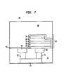
- FIG. 1With reference to the view of FIG. 1 , the invention is described with respect to formation and connection of an exemplary capacitor structure formed in three levels of interconnect metallization.
- a portion of an integrated circuit structure 10is shown in partial cross section to provide details of the invention in a metallization structure.
- the metallization structureis formed over a semiconductor layer (not illustrated) which typically will have a plurality of transistors in the surface thereof.
- several upper levels of metal interconnect, such as Al or Cu runnersare formed over the semiconductor layer according to a dual Damascene fabrication process.
- a portion of the integrated circuit structure 10is shown in FIG. 1 to include three sequentially formed levels of metallization 20 , 30 and 40 .
- One or more additional levels of metallizationmay be formed below level 20 and one or more additional levels of metallization may be formed above level 40 .
- the metal runners in each levelare formed along a plane such as illustrated by line 42 along level 20 .
- a capacitor structure 50is electrically connected to conductors in the illustrated levels of metallization.
- the capacitor structure 50includes alternating layers of conductor and insulator formed in vertical alignment with respect to an underlying plane such as plane 42 or the plane of the surface on which the structure is formed.
- the structure 50is wired to provide two capacitors in parallel.
- Three conductor layers 52 , 54 , and 56are isolated from one another by two intervening dielectric layers.
- One dielectric layer 58is formed between conductors 52 and 54 and the other dielectric layer 60 is formed between conductor layers 54 and 56 .
- the conductor layer 54is a capacitor plate common to a first capacitor formed with layers 52 and 58 and a second capacitor formed with layers 56 and 60 .
- a via portion 64 of metallization level 40contacts the conductor layer 54 to provide a common terminal for both capacitors.
- Another via portion 66 of metallization level 40makes connection with the conductor layer 56 to provide a second terminal for the capacitor formed by layers 54 , 56 and 60 .
- a conductor runner portion 68 of metallization level 30provides connection to the conductor plate layer 52 to provide a second connection for the capacitor formed by layers 52 , 54 and 58 .
- a via portion 72 in metallization level 30connects the conductive runner portion 68 to a conductive runner 74 in metallization level 20 .
- the conductor runner 74is connected through another via portion 72 to conductive runner portion 76 of level 30 .
- a via portion 78 of level 40connects the conductive runner portion 76 to the conductive runner 82 of level 40 to effect contact through the via portion 66 to the capacitor conductor 56 .
- a via portion 94(associated with an overlying level of metallization) provides connection of the plates 52 and 56 to other circuitry not illustrated. Alternately, this connection could be made to a lower level of metallization through the conductive runner 74 of level 20 .
- a via portion 96(also associated with an overlying level of metallization) provides connection of the common plate 54 through a conductive runner 98 of level 40 to other circuitry not illustrated.
- each level of metallizationis formed with an initial deposit of a dielectric layer such as the layer 70 of FIG. 2 .
- the levels 20 / 30 of metallizationare completed prior to formation of the capacitor structure 50 .
- the layer 70 of dielectric materialwill typically be multi-layered, formed with an etch stop such as silicon nitride and plannarized by chemical mechanical polishing (CMP). Desired configurations of the Cu conductor lines are patterned and etched in the dielectric material to form trench-like openings therein.
- conductive barrier materialsuch as Ta, TaN or TiN is deposited along the surfaces of the etched opening to prevent migration of copper which is subsequently deposited in the openings.
- the barrier metalmay be formed with chemical vapor deposition (CVD) or physical vapor deposition (PVD).
- the Cu depositionis initiated with deposit of a seed layer on the barrier material, followed by electro-plating of Cu (e.g., from Copper sulfate) to fill the openings.
- a seed layer on the barrier materialFor dual Damascene structures such as the illustrated levels 20 / 30 both the via portion (providing connection between different levels of metallization) and the conductor portion (providing conductor runners within a level of metallization) are formed in sequential pattern and etch steps, followed by deposit of the barrier layer material, a seed layer and then an electro-deposition of the Cu to completely fill the via portions and the conductor member portions of the openings.
- an annealmay be provided to stabilize the micro structure.
- the structureis polished to remove excess copper and barrier metal from the surface of the dielectric layer 70 . This sequence is repeated for each level of metallization until the final copper layer of interconnection is passivated and the structure is prepared for packaging and assembly.
- the conductor layers 52 , 54 , and 56may be formed of sputtered Ta or TaN or TiN. These layers may be deposited by physical vapor deposition (PVD) or chemical vapor deposition (CVD).
- the conductor layer 52will comprise a Ti/TiN or Ta/TaN stack to provide a diffusion barrier and assure suitable adhesion of the conductor layer 52 with the underlying dielectric layer 70 .
- a Ti/TiN stack having approximately 20 nm of Ti and approximately 40 nm of TiNmay be deposited by a sequential sputter at 400 C, followed by an anneal.
- the layers 54 and 56may also be deposited by sputter techniques with the identified materials.
- a wide variety of other conductive materialsare suitable.
- the dielectric layers 58 and 60may be silicon oxides deposited by CVD. The oxide may be formed from silane. Alternately, the dielectric layers 58 and 60 may be formed of TaO 5 .
- Other insulator materialsmay be chosen based on desired dielectric constants and requirements regarding minimum current leakage.
- the upper most conductor layer 56is patterned and etched to remove a portion thereof and begin formation of an opening 88 to provide electrical connection to the underlying layer 54 .
- the opening 88is formed through the layer 56 for connection to the layer 54
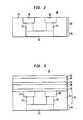
- all of the layers 52 , 54 , 56 , 58 and 60are pattered and etched in vertical alignment to fully define the capacitor structure 50 . That is, the etch defines vertically aligned layers with respect to an underlying plane such as the plane 42 or the plane along the surface of the dielectric layer 70 on which the structure 50 is formed. See next FIG.
- FIG. 6which illustrates a 60 nm barrier layer 80 of silicon nitride deposited on the exposed portions of layers 52 , 54 , 56 , 58 and 60 as well as the dielectric layer 70 and exposed regions of Cu in the metallization level 30 . See FIG. 5 .
- another dielectric layer 90is formed over the structure 10 by a conformal deposition such as high density plasma (HDP) deposition of silicon oxide.
- the dielectric layer 90is planarized by CMP, or by metal topographic reduction (MTR), wherein deposit of photoresist over low regions is followed by a standard etch.
- the planarized structure, ready for formation of the metallization level 40is illustrated in FIG. 7 .
- the via portions 64 and 66 and conductor members 82 and 98 of metallization level 40are then formed in the dielectric layer 90 as illustrated in FIG. 1 .
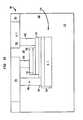
- the capacitor structure 50may also be connected in the circuit structure 10 with two levels of interconnect conductors as illustrated in FIG. 8.
- a lower conductor level 30includes a runner portion 123 effecting connection between lower plate 52 and a via portion 92 of level 40 . Other connections are as described with regard to FIG. 1 .
- stacks of three, four and more capacitorscan be fabricated in parallel connection with such stacks formed between two levels of conductor. See FIG. 9 which illustrates a stack comprising five conductor layers 122 sequentially deposited with intervening dielectric layers 124 positioned between pairs of layers 120 to provide capacitor dielectrics. Connections to individual layers 122 are made through via portions 126 and conductive runners 120 , 123 and 125 to configure four capacitors connected in parallel.
- FIG. 10illustrates the capacitor structure 250 including three sequentially formed metal layers 252 , 254 , and 256 with two intervening dielectric layers 262 positioned between pairs ( 252 , 254 ) and ( 254 , 256 ) of layers to provide capacitor dielectric.
- the structure 250is connected to configure two parallel capacitors.
- the lowest level 252 metal layermay be a runner in a level 270 of Al interconnect comprising Al—Cu alloy with an under-layer of Ti/TiN providing adhesion and a barrier against diffusion.
- the level 270is formed over a dielectric layer 272 .
- the layers 254 and 256may be deposited TiN.
- a second level 280 of Al interconnectis formed above the structure 250 in a dielectric layer 284 .
- Contacts 286extend through an interlevel dielectric layer 288 to configure the parallel capacitors in connection with two runners 290 and 292 in level 280 .
- all of the layers of the capacitor structure 250may be formed in vertical alignment, with the contact between runner 290 and layer 252 made through a connection to a metal runner below the level 270 (not illustrated).
Landscapes
- Engineering & Computer Science (AREA)
- Power Engineering (AREA)
- Physics & Mathematics (AREA)
- Condensed Matter Physics & Semiconductors (AREA)
- General Physics & Mathematics (AREA)
- Computer Hardware Design (AREA)
- Microelectronics & Electronic Packaging (AREA)
- Internal Circuitry In Semiconductor Integrated Circuit Devices (AREA)
- Semiconductor Integrated Circuits (AREA)
Abstract
Description
Claims (6)
Priority Applications (5)
| Application Number | Priority Date | Filing Date | Title |
|---|---|---|---|
| US09/653,295US6838717B1 (en) | 2000-08-31 | 2000-08-31 | Stacked structure for parallel capacitors and method of fabrication |
| TW090121470ATW515099B (en) | 2000-08-31 | 2001-08-30 | Stacked structure for parallel capacitors and method of fabrication |
| JP2001262599AJP2002141417A (en) | 2000-08-31 | 2001-08-31 | Stack structure of parallel capacitor and manufacturing method |
| GB0121201AGB2371147B (en) | 2000-08-31 | 2001-08-31 | Stacked structure for parallel capacitors and method of fabrication |
| KR1020010053297AKR100773256B1 (en) | 2000-08-31 | 2001-08-31 | Stacked structure for parallel capacitors and method of fabrication |
Applications Claiming Priority (1)
| Application Number | Priority Date | Filing Date | Title |
|---|---|---|---|
| US09/653,295US6838717B1 (en) | 2000-08-31 | 2000-08-31 | Stacked structure for parallel capacitors and method of fabrication |
Publications (1)
| Publication Number | Publication Date |
|---|---|
| US6838717B1true US6838717B1 (en) | 2005-01-04 |
Family
ID=24620268
Family Applications (1)
| Application Number | Title | Priority Date | Filing Date |
|---|---|---|---|
| US09/653,295Expired - LifetimeUS6838717B1 (en) | 2000-08-31 | 2000-08-31 | Stacked structure for parallel capacitors and method of fabrication |
Country Status (5)
| Country | Link |
|---|---|
| US (1) | US6838717B1 (en) |
| JP (1) | JP2002141417A (en) |
| KR (1) | KR100773256B1 (en) |
| GB (1) | GB2371147B (en) |
| TW (1) | TW515099B (en) |
Cited By (20)
| Publication number | Priority date | Publication date | Assignee | Title |
|---|---|---|---|---|
| US20020177287A1 (en)* | 2000-01-21 | 2002-11-28 | Lucent Technologies Inc. | Capacitor for integration with copper damascene processes and a method of manufacture therefore |
| US20050116276A1 (en)* | 2003-11-28 | 2005-06-02 | Jing-Horng Gau | Metal-insulator-metal (MIM) capacitor and fabrication method for making the same |
| US20050167722A1 (en)* | 2004-02-04 | 2005-08-04 | Won Seok-Jun | Semiconductor device having dual stacked MIM capacitor and method of fabricating the same |
| US20050272216A1 (en)* | 2004-03-10 | 2005-12-08 | Motorola, Inc. | Method of making a semiconductor device, and semiconductor device made thereby |
| US20050287755A1 (en)* | 2002-12-20 | 2005-12-29 | Jens Bachmann | Capacitor assemblies |
| US7078310B1 (en)* | 2003-05-28 | 2006-07-18 | Newport Fab, Llc | Method for fabricating a high density composite MIM capacitor with flexible routing in semiconductor dies |
| US20070069385A1 (en)* | 2005-09-13 | 2007-03-29 | Anthony Oates | MIM capacitor integrated into the damascene structure and method of making thereof |
| US20070105257A1 (en)* | 2005-11-08 | 2007-05-10 | Samsung Electronics Co., Ltd. | Methods of fabricating semiconductor devices |
| US20070205248A1 (en)* | 2006-03-01 | 2007-09-06 | Taiwan Semiconductor Manufacturing Company, Ltd. | Flexible processing method for metal-insulator-metal capacitor formation |
| US20080001256A1 (en)* | 2005-06-09 | 2008-01-03 | Freescale Semiconductors, Inc. | Semiconductor device comprising passive components |
| US20090096062A1 (en)* | 2007-10-16 | 2009-04-16 | Ki-Wan Bang | Stack capacitor in semiconductor device and method for fabricating the same |
| US7602599B1 (en)* | 2008-07-09 | 2009-10-13 | United Microelectronics Corp. | Metal-metal capacitor and method of making the same |
| US20100190315A1 (en)* | 2009-01-29 | 2010-07-29 | Hack Seob Shin | Method of manufacturing semiconductor memory device |
| US20110210420A1 (en)* | 2009-05-26 | 2011-09-01 | Stats Chippac, Ltd. | Semiconductor Device Having IPD Structure with Smooth Conductive Layer and Bottom-Side Conductive Layer |
| US20120126369A1 (en)* | 2006-12-21 | 2012-05-24 | Stats Chippac, Ltd. | Semiconductor Device and Method of Forming Passive Devices |
| WO2014201415A1 (en)* | 2013-06-13 | 2014-12-18 | Qualcomm Incorporated | Metal-insulator-metal capacitor structures |
| US9305994B2 (en) | 2014-06-05 | 2016-04-05 | United Microelectronics Corp. | Semiconductor apparatus with multi-layer capacitance structure |
| US9761655B1 (en) | 2016-06-20 | 2017-09-12 | International Business Machines Corporation | Stacked planar capacitors with scaled EOT |
| US20190206981A1 (en)* | 2017-12-29 | 2019-07-04 | Texas Instruments Incorporated | High voltage isolation structure and method |
| US10366832B2 (en) | 2015-02-27 | 2019-07-30 | Murata Manufacturing Co., Ltd. | Capacitor and electronic device having a plurality of surface electrodes electrically connected to each other by an intermediate electrode |
Families Citing this family (8)
| Publication number | Priority date | Publication date | Assignee | Title |
|---|---|---|---|---|
| US6784478B2 (en) | 2002-09-30 | 2004-08-31 | Agere Systems Inc. | Junction capacitor structure and fabrication method therefor in a dual damascene process |
| KR100480641B1 (en)* | 2002-10-17 | 2005-03-31 | 삼성전자주식회사 | Metal-Insulator-Metal capacitor having high capacitance, integrated circuit chip having the same and method for manufacturing the same |
| JP2004179419A (en) | 2002-11-27 | 2004-06-24 | Toshiba Corp | Semiconductor device and manufacturing method thereof |
| KR100505658B1 (en)* | 2002-12-11 | 2005-08-03 | 삼성전자주식회사 | Semiconductor device having MIM capacitor |
| US6680521B1 (en)* | 2003-04-09 | 2004-01-20 | Newport Fab, Llc | High density composite MIM capacitor with reduced voltage dependence in semiconductor dies |
| KR100695993B1 (en)* | 2004-12-30 | 2007-03-15 | 매그나칩 반도체 유한회사 | Multi-Layered MMC Capacitor and Manufacturing Method Thereof |
| KR100957881B1 (en) | 2007-12-28 | 2010-05-13 | 매그나칩 반도체 유한회사 | MIM Capacitor |
| JP2021077799A (en)* | 2019-11-12 | 2021-05-20 | ローム株式会社 | Electronic component |
Citations (5)
| Publication number | Priority date | Publication date | Assignee | Title |
|---|---|---|---|---|
| US3962713A (en)* | 1972-06-02 | 1976-06-08 | Texas Instruments Incorporated | Large value capacitor |
| US5481490A (en)* | 1993-10-12 | 1996-01-02 | Olympus Optical Co., Ltd. | Ferroelectric memory |
| US5643804A (en)* | 1993-05-21 | 1997-07-01 | Semiconductor Energy Laboratory Co., Ltd. | Method of manufacturing a hybrid integrated circuit component having a laminated body |
| US5736448A (en)* | 1995-12-04 | 1998-04-07 | General Electric Company | Fabrication method for thin film capacitors |
| US6180976B1 (en)* | 1999-02-02 | 2001-01-30 | Conexant Systems, Inc. | Thin-film capacitors and methods for forming the same |
Family Cites Families (5)
| Publication number | Priority date | Publication date | Assignee | Title |
|---|---|---|---|---|
| US5583359A (en)* | 1995-03-03 | 1996-12-10 | Northern Telecom Limited | Capacitor structure for an integrated circuit |
| US5926359A (en)* | 1996-04-01 | 1999-07-20 | International Business Machines Corporation | Metal-insulator-metal capacitor |
| US6066537A (en)* | 1998-02-02 | 2000-05-23 | Tritech Microelectronics, Ltd. | Method for fabricating a shielded multilevel integrated circuit capacitor |
| WO2000049660A1 (en)* | 1999-02-16 | 2000-08-24 | Symetrix Corporation | Iridium oxide diffusion barrier between local interconnect layer and thin film of layered superlattice material |
| JP3950290B2 (en)* | 1999-09-10 | 2007-07-25 | 三星電子株式会社 | Semiconductor memory device including capacitor protective film and method of manufacturing the same |
- 2000
- 2000-08-31USUS09/653,295patent/US6838717B1/ennot_activeExpired - Lifetime
- 2001
- 2001-08-30TWTW090121470Apatent/TW515099B/ennot_activeIP Right Cessation
- 2001-08-31GBGB0121201Apatent/GB2371147B/ennot_activeExpired - Fee Related
- 2001-08-31JPJP2001262599Apatent/JP2002141417A/ennot_activeWithdrawn
- 2001-08-31KRKR1020010053297Apatent/KR100773256B1/ennot_activeExpired - Lifetime
Patent Citations (5)
| Publication number | Priority date | Publication date | Assignee | Title |
|---|---|---|---|---|
| US3962713A (en)* | 1972-06-02 | 1976-06-08 | Texas Instruments Incorporated | Large value capacitor |
| US5643804A (en)* | 1993-05-21 | 1997-07-01 | Semiconductor Energy Laboratory Co., Ltd. | Method of manufacturing a hybrid integrated circuit component having a laminated body |
| US5481490A (en)* | 1993-10-12 | 1996-01-02 | Olympus Optical Co., Ltd. | Ferroelectric memory |
| US5736448A (en)* | 1995-12-04 | 1998-04-07 | General Electric Company | Fabrication method for thin film capacitors |
| US6180976B1 (en)* | 1999-02-02 | 2001-01-30 | Conexant Systems, Inc. | Thin-film capacitors and methods for forming the same |
Cited By (46)
| Publication number | Priority date | Publication date | Assignee | Title |
|---|---|---|---|---|
| US7135733B2 (en)* | 2000-01-21 | 2006-11-14 | Agere Systems Inc. | Capacitor for integration with copper damascene processes and a method of manufacture therefore |
| US20020177287A1 (en)* | 2000-01-21 | 2002-11-28 | Lucent Technologies Inc. | Capacitor for integration with copper damascene processes and a method of manufacture therefore |
| US8008161B2 (en)* | 2002-12-20 | 2011-08-30 | Infineon Technologies Ag | Capacitor assemblies |
| US20050287755A1 (en)* | 2002-12-20 | 2005-12-29 | Jens Bachmann | Capacitor assemblies |
| US7078310B1 (en)* | 2003-05-28 | 2006-07-18 | Newport Fab, Llc | Method for fabricating a high density composite MIM capacitor with flexible routing in semiconductor dies |
| US20050116276A1 (en)* | 2003-11-28 | 2005-06-02 | Jing-Horng Gau | Metal-insulator-metal (MIM) capacitor and fabrication method for making the same |
| US20050118778A1 (en)* | 2003-11-28 | 2005-06-02 | Jing-Horng Gau | Metal-insulator-metal (mim) capacitor and fabrication method for making the same |
| US6977198B2 (en) | 2003-11-28 | 2005-12-20 | United Microelectronics Corp. | Metal-insulator-metal (MIM) capacitor and fabrication method for making the same |
| US20070111496A1 (en)* | 2004-02-04 | 2007-05-17 | Won Seok-Jun | Semiconductor device having dual stacked MIM capacitor and method of fabricating the same |
| US20050167722A1 (en)* | 2004-02-04 | 2005-08-04 | Won Seok-Jun | Semiconductor device having dual stacked MIM capacitor and method of fabricating the same |
| US7338879B2 (en) | 2004-02-04 | 2008-03-04 | Samsung Electronics Co., Ltd. | Method of fabricating a semiconductor device having dual stacked MIM capacitor |
| US7180120B2 (en)* | 2004-02-04 | 2007-02-20 | Samsung Electronics Co., Ltd. | Semiconductor device having dual stacked MIM capacitor and method of fabricating the same |
| WO2005091795A3 (en)* | 2004-03-10 | 2005-12-15 | Freescale Semiconductor Inc | Method of making a semiconductor device, and semiconductor device made thereby |
| US7306986B2 (en) | 2004-03-10 | 2007-12-11 | Freescale Semiconductor, Inc. | Method of making a semiconductor device, and semiconductor device made thereby |
| US20050272216A1 (en)* | 2004-03-10 | 2005-12-08 | Motorola, Inc. | Method of making a semiconductor device, and semiconductor device made thereby |
| US20090224365A1 (en)* | 2004-03-10 | 2009-09-10 | Freescale Semiconductor, Inc. | Semiconductor Device Comprising Passive Components |
| US7898059B2 (en)* | 2004-03-10 | 2011-03-01 | Freescale Semiconductor, Inc. | Semiconductor device comprising passive components |
| US20080001256A1 (en)* | 2005-06-09 | 2008-01-03 | Freescale Semiconductors, Inc. | Semiconductor device comprising passive components |
| US7535079B2 (en) | 2005-06-09 | 2009-05-19 | Freescale Semiconductor, Inc. | Semiconductor device comprising passive components |
| US20070069385A1 (en)* | 2005-09-13 | 2007-03-29 | Anthony Oates | MIM capacitor integrated into the damascene structure and method of making thereof |
| US7768099B2 (en) | 2005-09-13 | 2010-08-03 | Taiwan Semiconductor Manufacturing Company, Ltd. | MIM capacitor integrated into the damascene structure and method of making thereof |
| US20070105257A1 (en)* | 2005-11-08 | 2007-05-10 | Samsung Electronics Co., Ltd. | Methods of fabricating semiconductor devices |
| US7491619B2 (en)* | 2005-11-08 | 2009-02-17 | Samsung Electronics Co., Ltd. | Methods of fabricating semiconductor devices |
| US9000562B2 (en) | 2006-03-01 | 2015-04-07 | Taiwan Semiconductor Manufacturing Company, Ltd. | Flexible processing method for metal-insulator-metal capacitor formation |
| US9312325B2 (en) | 2006-03-01 | 2016-04-12 | Taiwan Semiconductor Manufacturing Company, Ltd. | Semiconductor metal insulator metal capacitor device and method of manufacture |
| US20070205248A1 (en)* | 2006-03-01 | 2007-09-06 | Taiwan Semiconductor Manufacturing Company, Ltd. | Flexible processing method for metal-insulator-metal capacitor formation |
| US7964470B2 (en)* | 2006-03-01 | 2011-06-21 | Taiwan Semiconductor Manufacturing Company, Ltd. | Flexible processing method for metal-insulator-metal capacitor formation |
| US20120126369A1 (en)* | 2006-12-21 | 2012-05-24 | Stats Chippac, Ltd. | Semiconductor Device and Method of Forming Passive Devices |
| US9349723B2 (en)* | 2006-12-21 | 2016-05-24 | Stats Chippac, Ltd. | Semiconductor device and method of forming passive devices |
| US20090096062A1 (en)* | 2007-10-16 | 2009-04-16 | Ki-Wan Bang | Stack capacitor in semiconductor device and method for fabricating the same |
| DE102008048651B4 (en)* | 2007-10-16 | 2010-11-04 | Dongbu Hitek Co., Ltd. | Method of manufacturing a semiconductor device with two capacitors |
| US7943476B2 (en) | 2007-10-16 | 2011-05-17 | Dongbu Hitek Co., Ltd. | Stack capacitor in semiconductor device and method for fabricating the same including one electrode with greater surface area |
| US7602599B1 (en)* | 2008-07-09 | 2009-10-13 | United Microelectronics Corp. | Metal-metal capacitor and method of making the same |
| US20100190315A1 (en)* | 2009-01-29 | 2010-07-29 | Hack Seob Shin | Method of manufacturing semiconductor memory device |
| US9030002B2 (en)* | 2009-05-26 | 2015-05-12 | Stats Chippac, Ltd. | Semiconductor device having IPD structure with smooth conductive layer and bottom-side conductive layer |
| US20110210420A1 (en)* | 2009-05-26 | 2011-09-01 | Stats Chippac, Ltd. | Semiconductor Device Having IPD Structure with Smooth Conductive Layer and Bottom-Side Conductive Layer |
| US9041148B2 (en) | 2013-06-13 | 2015-05-26 | Qualcomm Incorporated | Metal-insulator-metal capacitor structures |
| US9312326B2 (en) | 2013-06-13 | 2016-04-12 | Qualcomm Incorporated | Metal-insulator-metal capacitor structures |
| WO2014201415A1 (en)* | 2013-06-13 | 2014-12-18 | Qualcomm Incorporated | Metal-insulator-metal capacitor structures |
| CN105324862B (en)* | 2013-06-13 | 2017-06-23 | 高通股份有限公司 | Metal-insulator-metal capacitor structure |
| CN107180813A (en)* | 2013-06-13 | 2017-09-19 | 高通股份有限公司 | metal-insulator-metal capacitor structure |
| US9305994B2 (en) | 2014-06-05 | 2016-04-05 | United Microelectronics Corp. | Semiconductor apparatus with multi-layer capacitance structure |
| US10366832B2 (en) | 2015-02-27 | 2019-07-30 | Murata Manufacturing Co., Ltd. | Capacitor and electronic device having a plurality of surface electrodes electrically connected to each other by an intermediate electrode |
| US9761655B1 (en) | 2016-06-20 | 2017-09-12 | International Business Machines Corporation | Stacked planar capacitors with scaled EOT |
| US20190206981A1 (en)* | 2017-12-29 | 2019-07-04 | Texas Instruments Incorporated | High voltage isolation structure and method |
| US11222945B2 (en)* | 2017-12-29 | 2022-01-11 | Texas Instruments Incorporated | High voltage isolation structure and method |
Also Published As
| Publication number | Publication date |
|---|---|
| GB0121201D0 (en) | 2001-10-24 |
| JP2002141417A (en) | 2002-05-17 |
| GB2371147B (en) | 2005-04-13 |
| GB2371147A (en) | 2002-07-17 |
| KR20020018603A (en) | 2002-03-08 |
| KR100773256B1 (en) | 2007-11-05 |
| TW515099B (en) | 2002-12-21 |
Similar Documents
| Publication | Publication Date | Title |
|---|---|---|
| US6838717B1 (en) | Stacked structure for parallel capacitors and method of fabrication | |
| JP3778487B2 (en) | Method for forming metal capacitor | |
| EP0852065B1 (en) | Interconnect scheme for integrated circuits | |
| US7538005B2 (en) | Semiconductor device and method for fabricating the same | |
| CN1194418C (en) | Integrated component comprising metal-insulator-metal capacitor | |
| JP3895126B2 (en) | Manufacturing method of semiconductor device | |
| JP3715502B2 (en) | Semiconductor device and manufacturing method thereof | |
| JP4386680B2 (en) | Capacitor for semiconductor device and manufacturing method thereof | |
| JP2003297942A (en) | Semiconductor device having metal-insulator-metal capacitor and method thereof | |
| US11769722B2 (en) | Method of forming a metal-insulator-metal (MIM) capacitor | |
| JPH09162354A (en) | Integrated inductor structure and its manufacture | |
| US6746951B2 (en) | Bond pad of semiconductor device and method of fabricating the same | |
| US20060012052A1 (en) | Dual damascene wiring and method | |
| US7586142B2 (en) | Semiconductor device having metal-insulator-metal capacitor and method of fabricating the same | |
| US9177908B2 (en) | Stacked semiconductor capacitor structure | |
| US6391713B1 (en) | Method for forming a dual damascene structure having capacitors | |
| US6838352B1 (en) | Damascene trench capacitor for mixed-signal/RF IC applications | |
| US6410386B1 (en) | Method for forming a metal capacitor in a damascene process | |
| US20020190299A1 (en) | Metal capacitor in damascene structures | |
| JP2000208743A (en) | Integrated circuit device provided with dual damascene capacitor and related method for manufacture | |
| CN101317270A (en) | High-density high-Q capacitors on top of protective layer | |
| CN100373546C (en) | Method for manufacturing metal-insulating layer-metal capacitor | |
| KR101133527B1 (en) | Method of forming semiconductor device |
Legal Events
| Date | Code | Title | Description |
|---|---|---|---|
| AS | Assignment | Owner name:LUCENT TECHNOLOGIES, INC., NEW JERSEY Free format text:ASSIGNMENT OF ASSIGNORS INTEREST;ASSIGNORS:YEN, ALLEN;HUI, FRANK YAUCHEE;YAN, YIFENG WINSTON;REEL/FRAME:011432/0451;SIGNING DATES FROM 20001201 TO 20001206 | |
| FEPP | Fee payment procedure | Free format text:PAYER NUMBER DE-ASSIGNED (ORIGINAL EVENT CODE: RMPN); ENTITY STATUS OF PATENT OWNER: LARGE ENTITY Free format text:PAYOR NUMBER ASSIGNED (ORIGINAL EVENT CODE: ASPN); ENTITY STATUS OF PATENT OWNER: LARGE ENTITY | |
| STCF | Information on status: patent grant | Free format text:PATENTED CASE | |
| FPAY | Fee payment | Year of fee payment:4 | |
| FPAY | Fee payment | Year of fee payment:8 | |
| AS | Assignment | Owner name:DEUTSCHE BANK AG NEW YORK BRANCH, AS COLLATERAL AG Free format text:PATENT SECURITY AGREEMENT;ASSIGNORS:LSI CORPORATION;AGERE SYSTEMS LLC;REEL/FRAME:032856/0031 Effective date:20140506 | |
| AS | Assignment | Owner name:AVAGO TECHNOLOGIES GENERAL IP (SINGAPORE) PTE. LTD Free format text:ASSIGNMENT OF ASSIGNORS INTEREST;ASSIGNOR:AGERE SYSTEMS LLC;REEL/FRAME:035365/0634 Effective date:20140804 | |
| AS | Assignment | Owner name:AGERE SYSTEMS LLC, PENNSYLVANIA Free format text:TERMINATION AND RELEASE OF SECURITY INTEREST IN PATENT RIGHTS (RELEASES RF 032856-0031);ASSIGNOR:DEUTSCHE BANK AG NEW YORK BRANCH, AS COLLATERAL AGENT;REEL/FRAME:037684/0039 Effective date:20160201 Owner name:LSI CORPORATION, CALIFORNIA Free format text:TERMINATION AND RELEASE OF SECURITY INTEREST IN PATENT RIGHTS (RELEASES RF 032856-0031);ASSIGNOR:DEUTSCHE BANK AG NEW YORK BRANCH, AS COLLATERAL AGENT;REEL/FRAME:037684/0039 Effective date:20160201 | |
| AS | Assignment | Owner name:BANK OF AMERICA, N.A., AS COLLATERAL AGENT, NORTH CAROLINA Free format text:PATENT SECURITY AGREEMENT;ASSIGNOR:AVAGO TECHNOLOGIES GENERAL IP (SINGAPORE) PTE. LTD.;REEL/FRAME:037808/0001 Effective date:20160201 Owner name:BANK OF AMERICA, N.A., AS COLLATERAL AGENT, NORTH Free format text:PATENT SECURITY AGREEMENT;ASSIGNOR:AVAGO TECHNOLOGIES GENERAL IP (SINGAPORE) PTE. LTD.;REEL/FRAME:037808/0001 Effective date:20160201 | |
| FPAY | Fee payment | Year of fee payment:12 | |
| AS | Assignment | Owner name:AVAGO TECHNOLOGIES GENERAL IP (SINGAPORE) PTE. LTD., SINGAPORE Free format text:TERMINATION AND RELEASE OF SECURITY INTEREST IN PATENTS;ASSIGNOR:BANK OF AMERICA, N.A., AS COLLATERAL AGENT;REEL/FRAME:041710/0001 Effective date:20170119 Owner name:AVAGO TECHNOLOGIES GENERAL IP (SINGAPORE) PTE. LTD Free format text:TERMINATION AND RELEASE OF SECURITY INTEREST IN PATENTS;ASSIGNOR:BANK OF AMERICA, N.A., AS COLLATERAL AGENT;REEL/FRAME:041710/0001 Effective date:20170119 | |
| AS | Assignment | Owner name:BELL SEMICONDUCTOR, LLC, ILLINOIS Free format text:ASSIGNMENT OF ASSIGNORS INTEREST;ASSIGNORS:AVAGO TECHNOLOGIES GENERAL IP (SINGAPORE) PTE. LTD.;BROADCOM CORPORATION;REEL/FRAME:044886/0608 Effective date:20171208 | |
| AS | Assignment | Owner name:CORTLAND CAPITAL MARKET SERVICES LLC, AS COLLATERA Free format text:SECURITY INTEREST;ASSIGNORS:HILCO PATENT ACQUISITION 56, LLC;BELL SEMICONDUCTOR, LLC;BELL NORTHERN RESEARCH, LLC;REEL/FRAME:045216/0020 Effective date:20180124 | |
| AS | Assignment | Owner name:BELL NORTHERN RESEARCH, LLC, ILLINOIS Free format text:RELEASE BY SECURED PARTY;ASSIGNOR:CORTLAND CAPITAL MARKET SERVICES LLC;REEL/FRAME:059720/0719 Effective date:20220401 Owner name:BELL SEMICONDUCTOR, LLC, ILLINOIS Free format text:RELEASE BY SECURED PARTY;ASSIGNOR:CORTLAND CAPITAL MARKET SERVICES LLC;REEL/FRAME:059720/0719 Effective date:20220401 Owner name:HILCO PATENT ACQUISITION 56, LLC, ILLINOIS Free format text:RELEASE BY SECURED PARTY;ASSIGNOR:CORTLAND CAPITAL MARKET SERVICES LLC;REEL/FRAME:059720/0719 Effective date:20220401 |