US6838380B2 - Fabrication of high resistivity structures using focused ion beams - Google Patents
Fabrication of high resistivity structures using focused ion beamsDownload PDFInfo
- Publication number
- US6838380B2 US6838380B2US10/055,320US5532002AUS6838380B2US 6838380 B2US6838380 B2US 6838380B2US 5532002 AUS5532002 AUS 5532002AUS 6838380 B2US6838380 B2US 6838380B2
- Authority
- US
- United States
- Prior art keywords
- precursor
- ion beam
- target
- precursor compound
- compound
- Prior art date
- Legal status (The legal status is an assumption and is not a legal conclusion. Google has not performed a legal analysis and makes no representation as to the accuracy of the status listed.)
- Expired - Lifetime, expires
Links
- 238000010884ion-beam techniqueMethods0.000titleclaimsabstractdescription74
- 238000004519manufacturing processMethods0.000titledescription6
- 239000002243precursorSubstances0.000claimsabstractdescription100
- 150000001875compoundsChemical class0.000claimsabstractdescription63
- 238000000034methodMethods0.000claimsabstractdescription52
- 239000007789gasSubstances0.000claimsdescription55
- 239000004020conductorSubstances0.000claimsdescription39
- 230000008021depositionEffects0.000claimsdescription13
- 239000000523sampleSubstances0.000claimsdescription10
- -1tungsten organometallic compoundChemical class0.000claimsdescription8
- 239000011810insulating materialSubstances0.000claimsdescription7
- WZJUBBHODHNQPW-UHFFFAOYSA-N2,4,6,8-tetramethyl-1,3,5,7,2$l^{3},4$l^{3},6$l^{3},8$l^{3}-tetraoxatetrasilocaneChemical compoundC[Si]1O[Si](C)O[Si](C)O[Si](C)O1WZJUBBHODHNQPW-UHFFFAOYSA-N0.000claimsdescription4
- 150000002902organometallic compoundsChemical class0.000claimsdescription4
- BASFCYQUMIYNBI-UHFFFAOYSA-NplatinumChemical compound[Pt]BASFCYQUMIYNBI-UHFFFAOYSA-N0.000claimsdescription4
- HMMGMWAXVFQUOA-UHFFFAOYSA-NoctamethylcyclotetrasiloxaneChemical compoundC[Si]1(C)O[Si](C)(C)O[Si](C)(C)O[Si](C)(C)O1HMMGMWAXVFQUOA-UHFFFAOYSA-N0.000claimsdescription3
- 229910052721tungstenInorganic materials0.000claimsdescription3
- 239000010937tungstenSubstances0.000claimsdescription3
- 229910052697platinumInorganic materials0.000claimsdescription2
- 229910052710siliconInorganic materials0.000claims1
- 239000010703siliconSubstances0.000claims1
- 230000001747exhibiting effectEffects0.000abstractdescription4
- 239000000463materialSubstances0.000description17
- 238000000151depositionMethods0.000description16
- 239000002245particleSubstances0.000description10
- 239000012530fluidSubstances0.000description9
- 150000002500ionsChemical class0.000description7
- 239000000203mixtureSubstances0.000description7
- 230000008569processEffects0.000description7
- KPUWHANPEXNPJT-UHFFFAOYSA-NdisiloxaneChemical class[SiH3]O[SiH3]KPUWHANPEXNPJT-UHFFFAOYSA-N0.000description6
- 238000002347injectionMethods0.000description6
- 239000007924injectionSubstances0.000description6
- 239000012777electrically insulating materialSubstances0.000description3
- 239000012212insulatorSubstances0.000description3
- 229910052751metalInorganic materials0.000description3
- 239000002184metalSubstances0.000description3
- 238000001465metallisationMethods0.000description3
- FQNHWXHRAUXLFU-UHFFFAOYSA-Ncarbon monoxide;tungstenChemical group[W].[O+]#[C-].[O+]#[C-].[O+]#[C-].[O+]#[C-].[O+]#[C-].[O+]#[C-]FQNHWXHRAUXLFU-UHFFFAOYSA-N0.000description2
- 230000008859changeEffects0.000description2
- 238000005530etchingMethods0.000description2
- 238000003384imaging methodMethods0.000description2
- 229910001338liquidmetalInorganic materials0.000description2
- 238000005259measurementMethods0.000description2
- 239000007769metal materialSubstances0.000description2
- 150000002739metalsChemical group0.000description2
- 239000004065semiconductorSubstances0.000description2
- 238000012360testing methodMethods0.000description2
- 238000004804windingMethods0.000description2
- 108010083687Ion PumpsProteins0.000description1
- 230000001133accelerationEffects0.000description1
- 230000004075alterationEffects0.000description1
- 238000010276constructionMethods0.000description1
- 238000000354decomposition reactionMethods0.000description1
- 230000000779depleting effectEffects0.000description1
- 238000005137deposition processMethods0.000description1
- 238000009826distributionMethods0.000description1
- 238000010894electron beam technologyMethods0.000description1
- 238000002474experimental methodMethods0.000description1
- 229910052733galliumInorganic materials0.000description1
- 150000002484inorganic compoundsChemical class0.000description1
- 229910010272inorganic materialInorganic materials0.000description1
- 238000007735ion beam assisted depositionMethods0.000description1
- 238000007737ion beam depositionMethods0.000description1
- 238000001888ion beam-induced depositionMethods0.000description1
- 230000007246mechanismEffects0.000description1
- 229910021645metal ionInorganic materials0.000description1
- 238000004377microelectronicMethods0.000description1
- 238000003801millingMethods0.000description1
- 238000002156mixingMethods0.000description1
- 230000004048modificationEffects0.000description1
- 238000012986modificationMethods0.000description1
- 230000003287optical effectEffects0.000description1
- 238000000206photolithographyMethods0.000description1
- 238000012545processingMethods0.000description1
- 238000005086pumpingMethods0.000description1
- 238000004544sputter depositionMethods0.000description1
- 238000000992sputter etchingMethods0.000description1
- 238000006467substitution reactionMethods0.000description1
- WFKWXMTUELFFGS-UHFFFAOYSA-NtungstenChemical compound[W]WFKWXMTUELFFGS-UHFFFAOYSA-N0.000description1
- 235000012431wafersNutrition0.000description1
Images


Classifications
- H—ELECTRICITY
- H10—SEMICONDUCTOR DEVICES; ELECTRIC SOLID-STATE DEVICES NOT OTHERWISE PROVIDED FOR
- H10D—INORGANIC ELECTRIC SEMICONDUCTOR DEVICES
- H10D1/00—Resistors, capacitors or inductors
- H10D1/40—Resistors
- H10D1/47—Resistors having no potential barriers
- H10D1/474—Resistors having no potential barriers comprising refractory metals, transition metals, noble metals, metal compounds or metal alloys, e.g. silicides
- C—CHEMISTRY; METALLURGY
- C23—COATING METALLIC MATERIAL; COATING MATERIAL WITH METALLIC MATERIAL; CHEMICAL SURFACE TREATMENT; DIFFUSION TREATMENT OF METALLIC MATERIAL; COATING BY VACUUM EVAPORATION, BY SPUTTERING, BY ION IMPLANTATION OR BY CHEMICAL VAPOUR DEPOSITION, IN GENERAL; INHIBITING CORROSION OF METALLIC MATERIAL OR INCRUSTATION IN GENERAL
- C23C—COATING METALLIC MATERIAL; COATING MATERIAL WITH METALLIC MATERIAL; SURFACE TREATMENT OF METALLIC MATERIAL BY DIFFUSION INTO THE SURFACE, BY CHEMICAL CONVERSION OR SUBSTITUTION; COATING BY VACUUM EVAPORATION, BY SPUTTERING, BY ION IMPLANTATION OR BY CHEMICAL VAPOUR DEPOSITION, IN GENERAL
- C23C16/00—Chemical coating by decomposition of gaseous compounds, without leaving reaction products of surface material in the coating, i.e. chemical vapour deposition [CVD] processes
- C23C16/04—Coating on selected surface areas, e.g. using masks
- C23C16/047—Coating on selected surface areas, e.g. using masks using irradiation by energy or particles
- H—ELECTRICITY
- H01—ELECTRIC ELEMENTS
- H01J—ELECTRIC DISCHARGE TUBES OR DISCHARGE LAMPS
- H01J37/00—Discharge tubes with provision for introducing objects or material to be exposed to the discharge, e.g. for the purpose of examination or processing thereof
- H01J37/02—Details
- H01J37/04—Arrangements of electrodes and associated parts for generating or controlling the discharge, e.g. electron-optical arrangement or ion-optical arrangement
- H01J37/08—Ion sources; Ion guns
- H—ELECTRICITY
- H01—ELECTRIC ELEMENTS
- H01L—SEMICONDUCTOR DEVICES NOT COVERED BY CLASS H10
- H01L21/00—Processes or apparatus adapted for the manufacture or treatment of semiconductor or solid state devices or of parts thereof
- H01L21/02—Manufacture or treatment of semiconductor devices or of parts thereof
- H01L21/04—Manufacture or treatment of semiconductor devices or of parts thereof the devices having potential barriers, e.g. a PN junction, depletion layer or carrier concentration layer
- H01L21/18—Manufacture or treatment of semiconductor devices or of parts thereof the devices having potential barriers, e.g. a PN junction, depletion layer or carrier concentration layer the devices having semiconductor bodies comprising elements of Group IV of the Periodic Table or AIIIBV compounds with or without impurities, e.g. doping materials
- H01L21/28—Manufacture of electrodes on semiconductor bodies using processes or apparatus not provided for in groups H01L21/20 - H01L21/268
- H01L21/283—Deposition of conductive or insulating materials for electrodes conducting electric current
- H01L21/285—Deposition of conductive or insulating materials for electrodes conducting electric current from a gas or vapour, e.g. condensation
- H01L21/28506—Deposition of conductive or insulating materials for electrodes conducting electric current from a gas or vapour, e.g. condensation of conductive layers
- H01L21/28512—Deposition of conductive or insulating materials for electrodes conducting electric current from a gas or vapour, e.g. condensation of conductive layers on semiconductor bodies comprising elements of Group IV of the Periodic Table
- H01L21/28556—Deposition of conductive or insulating materials for electrodes conducting electric current from a gas or vapour, e.g. condensation of conductive layers on semiconductor bodies comprising elements of Group IV of the Periodic Table by chemical means, e.g. CVD, LPCVD, PECVD, laser CVD
- H01L21/28562—Selective deposition
- H—ELECTRICITY
- H01—ELECTRIC ELEMENTS
- H01J—ELECTRIC DISCHARGE TUBES OR DISCHARGE LAMPS
- H01J2237/00—Discharge tubes exposing object to beam, e.g. for analysis treatment, etching, imaging
- H01J2237/30—Electron or ion beam tubes for processing objects
- H01J2237/317—Processing objects on a microscale
- H01J2237/31735—Direct-write microstructures
- H01J2237/31737—Direct-write microstructures using ions
- H—ELECTRICITY
- H01—ELECTRIC ELEMENTS
- H01J—ELECTRIC DISCHARGE TUBES OR DISCHARGE LAMPS
- H01J2237/00—Discharge tubes exposing object to beam, e.g. for analysis treatment, etching, imaging
- H01J2237/30—Electron or ion beam tubes for processing objects
- H01J2237/317—Processing objects on a microscale
- H01J2237/31749—Focused ion beam
Definitions
- the inventionrelates to the use of charged particle beam systems to fabricate conductive microscopic structures having high electrical resistivity and, in particular, to the use of focused ion beam systems to fabricate electronic circuit elements.
- Focused ion beamscan be focused to a spot smaller than one tenth of a micron. Because of their small spot size, focused ion beam systems are used to create and alter microscopic structures. Focused ion beams can micro-machine material by sputtering or etching, that is, physically knocking atoms or molecules from the target surface. Focused ion beams can also be used to deposit material, using a precursor gas that adheres to the specimen surface and decomposes in the presence of the ion beam to leave a deposit on the surface. FIB systems are widely used in the semiconductor industry to alter prototype integrated circuits by depositing metallic paths to create new connections and by etching metallic paths to eliminate connections. Using a FIB system to alter a circuit allows a circuit designer to test variations of the circuit without undertaking the lengthy process of modifying the photolithography masks and fabricating a new circuit from scratch.
- the system operatordirects a jet of precursor gas, typically an organometallic compound such as tungsten hexacarbonyl, to the surface of the specimen while a focused ion beam scans the area upon which the conductor is to be deposited.
- a metallic layeris deposited only in the area impacted by the beam. Because the ion beam can be focused to a diameter of less than one tenth of a micron, a very fine conductor can be deposited.
- An ion beam assisted deposition processis described, for example, in U.S. Pat. No. 4,876,112 to Kaito et al. for a “Process for Forming Metallic Patterned Film” and U.S. Pat. No. 5,104,684 to Tao et al. for “Ion Beam Induced Deposition of Metals.”
- a circuit designerneeds to include in his circuit a conductive element having greater electrical resistance than the deposited metallic conductor described above.
- Current ion beam deposition methodsthat deposit tungsten or other metal-based materials by the decomposition of precursor gases are incapable of depositing conductors having high electrical resistance.
- the electrical resistance of any particular conductoris determined by its resistivity, which is a property of the material itself, and its dimensions.
- the resistanceis equal to the resistivity divided by the cross sectional area of the conductor multiplied by its length. That is, for conductors composed of materials having the same resistivity, a longer conductor has more resistance than a shorter one and a thinner conductor has greater resistance than a thicker one.
- the resistivities of typical ion-beam deposited materialsare typically in the range of between one hundred micro-ohm-centimeter and five hundred micro-ohm-centimeter. While these resistivity values are much higher than those of bulk metals, the typical microscopic dimensions of microcircuit connections result in typical resistances of around 100 ohms. Such a low resistance is effectively a short circuit between the points it connects.
- An object of the inventionis to provide microscopic conductive structures having high electrical resistance.
- the inventionis particularly well suited to creating such structures in integrated micro-electronic circuits.
- the inventionentails using a charged particle beam to activate a precursor gas or gases, thereby depositing a material having a resistivity between that of an ion beam deposited metal material and an ion beam deposited insulator material.
- a charged particle beamto activate a precursor gas or gases, thereby depositing a material having a resistivity between that of an ion beam deposited metal material and an ion beam deposited insulator material.
- the preferred precursor gascomprises two gaseous compounds: a first gaseous compound that when directed toward a target in the presence of a charged particle beam and without the presence of other gases results in the deposition of a conductive material and a second gaseous compound that when directed toward a target in the presence of a charged particle beam and without the presence of other gases results in the deposition of an insulating material.
- FIG. 1is a focused ion beam system used to deposit a high resistivity material in accordance with the present invention
- FIG. 2shows a portion of a gas injection system of the present invention.
- FIG. 3is flow chart showing the steps of a preferred method of the present invention.
- FIG. 1shows schematically a typical focused ion beam system 8 used to implement a preferred embodiment of the present invention.
- Focused ion beam system 8includes an evacuated envelope 10 having an upper neck portion 12 within which are located a liquid metal ion source 14 and a focusing column 16 including extractor electrodes and an electrostatic optical system.
- Ion beam 18passes from source 14 through column 16 and between electrostatic deflection mechanism schematically indicated at 20 toward specimen 22 , which comprises, for example, a semiconductor device positioned on movable X-Y stage 24 within lower chamber 26 .
- Lower chamber 26can be vacuum isolated from evacuated envelope 10 by a valve 62 .
- An ultra high vacuum pumpsuch as an ion pump 28 , is employed for evacuating neck portion 12 .
- the chamber 26is evacuated with turbo-molecular and mechanical pumping system 30 under the control of vacuum controller 32 .
- the vacuum systemprovides within chamber 26 a vacuum of between approximately 1 ⁇ 10 ⁇ 7 Torr and 5 ⁇ 10 ⁇ 4 Torr.
- the chamber background pressureis typically about 1 ⁇ 10 ⁇ 5 Torr.
- High voltage power supply 34is connected to liquid metal ion source 14 as well as to appropriate electrodes in focusing column 16 for forming an approximately 1 keV to 60 keV ion beam 18 and directing the same downwardly.
- Deflection controller and amplifier 36operated in accordance with a prescribed pattern provided by pattern generator 38 , is coupled to deflection plates 20 whereby beam 18 may be controlled to trace out a corresponding pattern on the upper surface of specimen 22 .
- the deflection platesare placed before the final lens, as is well known in the art.
- the source 14typically provides a metal ion beam of gallium ions, although other ions and ion sources, such as a multi-cusp or other plasma ion source, can be used.
- the sourcetypically is capable of being focused into a sub-one-tenth micron wide beam at specimen 22 for either modifying the surface of specimen 22 by ion milling, enhanced etch, material deposition, or for the purpose of imaging the surface of specimen 22 .
- a charged particle multiplier 40 used for detecting secondary ion or electron emission for imagingis connected to video circuit and amplifier 42 , the latter supplying drive for a video monitor 44 , which also receives deflection signals from controller 36 .
- the location of charged particle multiplier 40 within chamber 26can vary in different embodiments.
- a scanning electron microscope 41along with its power supply and controls 45 , are optionally provided with the FIB system 8 .
- FIB system 8includes a fluid delivery system 46 for introducing and directing gaseous vapor toward specimen 22 .
- a fluid delivery system 46for introducing and directing gaseous vapor toward specimen 22 .
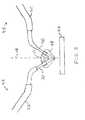
- FIG. 2shows an enlarged view of a portion of fluid delivery system 46 .
- Fluid delivery system 46includes a concentrator 48 and one or more fluid conduits 50 with corresponding extension arms 52 .
- Concentrator 48includes an aperture 54 allowing passage of ion beam 18 and inlets for accepting fluid conduits 50 .
- gas delivery system 46could comprise two independent gas sources, each having a nozzle at the end of a gas passage, to direct two jets of gaseous compounds toward the impact point of the focused ion beam.
- Another gas delivery systemis described in U.S. Pat. No. 5,435,850 to Rasmussen for a “Gas Injection System.”
- a door 60( FIG. 1 ) is opened for inserting specimen 22 on stage 24 which may be heated or cooled.
- the dooris interlocked so that it cannot be opened if the system is under vacuum.
- the high voltage power supplyprovides an appropriate acceleration voltage to electrodes in ion beam column 16 for energizing and focusing ion beam 18 .
- Focused ion beam systemsare commercially available, for example, from FEI Company, Hillsboro, Oreg. the assignee of the present application.
- a high resistivity materialis deposited on a specimen 22 by directing focused ion beam 18 toward an impact point on the specimen 22 and directing one or more precursor gases toward the ion beam impact point, the ion beam causing the precursor gas to decompose and thereby deposit a structure exhibiting high resistivity onto the target.
- the high resistivity materialcan be deposited in a precisely defined pattern.
- the resistance of the deposited structurescan be controlled.
- two independent gas injection systemsoperate to simultaneously provide two gaseous compounds at the impact point of the focused ion beam.
- the first compoundif injected individually, would decompose in the presence of the ion beam to deposit an electrically conductive material.
- the second compoundif injected individually, would decompose in the presence of the ion beam to deposit an electrically insulating material.
- the first compoundcomprises a metal precursor, for example, an organometallic compound such as tungsten hexacarbonyl
- the second compoundcomprises an insulating material precursor, for example, a siloxane compound such as tetramethylcyclotetrasiloxane (TMCTS).
- TCTStetramethylcyclotetrasiloxane
- step 204x-y stage 24 is moved to position the region at which the high resistivity material is to be deposited on specimen 22 within the scan area of focused ion beam 18 .
- step 206an insulator precursor gaseous compound is directed toward the specimen 22 .
- step 208a conductor precursor gaseous compound is directed toward the specimen 22 .
- the ion beam 18is directed in step 210 in a pattern corresponding to the structure that is to be deposited.
- the pattern to be depositedcan be designated by a system operator on monitor 44 and pattern generator 38 can cause deflection controller and amplifier 36 to control deflection electrodes 20 to cause beam 18 to scan the designated pattern.
- Optional step 212shows that the deposited structure is trimmed using the focused ion beam to obtain a structure having the desired resistance value to a high degree of precision.
- step 206entails directing a siloxane compound from concentrator 48 or from a nozzle of gas injection system 46 toward the specimen 22 .
- a siloxane compoundfrom concentrator 48 or from a nozzle of gas injection system 46 toward the specimen 22 .
- Only a small amount of siloxaneis required, and applicants have found that adjusting gas injection system 46 to a baratron pressure setting of 0.2 Torr provides an adequate amount of siloxane in an FEI 8000 Series FIB system. Skilled persons will understand that the gas pressure at the sample in the chamber is only indirectly related to the pressure in the gas injection system. The required pressure will vary from system to system and can be readily determined by varying the pressure until the desired results are achieved. Increasing the siloxane concentration was found to result in faster growth and increased contact resistance, but no change in the conductivity of the deposited structure.
- step 208entails directing a standard precursor for metal deposition directed toward specimen 22 .
- the siloxane gas and the metal deposition precursor gasmix in concentrator 48 and near the surface of specimen 22 . If separate nozzles are used for each gas, the gases mix near the surface of specimen 22 rather than in a concentrator.
- the method of delivering and mixing the gasesis not critical, and any method that delivers the gases to the surface at the impact point of the ion beam is suitable. Some precursor compounds can be premixed and flow through a single gas distribution system, but some precursor gases are reactive and should not be mixed beforehand.
- step 210comprises directing a 569 pico-ampere, 50 kilovolt beam toward specimen 22 , using conventional beam parameter settings, such as pixel spacing and beam dwell time, as appropriate for the structure to be deposited.
- a typical pixel spacingis 0.07 microns, with the primary ion beam dwelling at each pixel for about 0.5 microseconds.
- a typical refresh ratethat is, the time required to return to each pixel, is approximately 3,500 microseconds.
- the ion beam parameters and gas flow parametersare adjusted to avoid the ion beam depleting the precursor gas adhered to the surface during a dwell period while minimizing the unreacted precursor gas that must be exhausted from the vacuum chamber.
- Precursor gasses for metal depositionmay include a platinum or tungsten organometallic or inorganic compounds, as well as compounds of other conductors.
- the flow rate of such organometallic compoundcan typically be controlled by controlling the temperature of the chamber in which the precursor material is stored.
- Suitable siloxane compounds for use as the insulating material precursor compoundinclude TMCTS and octamethylcyclotetrasiloxane (OMCTS).
- OMCTSoctamethylcyclotetrasiloxane
- the siloxane compoundsrequire a valved fluid delivery system, such as the gas delivery system described in U.S. Pat. No. 5,851,413.
- test waferswere formed having a four point probe configuration that allowed measurement of both the resistivity and contact resistance of the deposited high resistivity structure.
- a large variety of structureswere tested to determine their resistance characteristics using the four point probe method.
- the resistivities of deposited resistive structureswere measured to be between about 5 ⁇ 10 4 ohms per square and about 7 ⁇ 10 4 ohms per square.
- Contact resistanceswere measured and found to be between one megohm and two megohms, although the contact resistance may vary with the precursor gases used. Further, deposited structures, measured by both the two and four point probe methods, exhibited linear current-voltage characteristics over a voltage range of greater than ten volts. Voltages within the linear voltage-current range are suitable for operation of typical integrated circuits.
- the resistance of structures deposited in accordance with the inventioncan be varied by varying the width and length of the resistive deposition, thus allowing a specific resistance value to be achieved.
- the resistances of structuresmeasured by both the two point probe method and the four point probe method, were inversely proportional to the width of the deposited conductor.
- a structure of a desired resistancecan be constructed by depositing a high resistivity conductor of the appropriate width, which can be readily determined once a deposition process is characterized for specific precursor compounds and flow rates and ion beam parameters.
- a deposited structurecan have its resistance increased to a specified value by FIB milling of the deposition following measurement of its resistance.
- Typical structurescan have widths typical of those currently deposited by focused ion beams. Such widths can be less than a few microns, less than one micron, or even less than 0.5 microns.
- the method of the inventioncan produce resistive structures, for example, less than 1000 ⁇ m long, and having resistances of greater than 100 kilohm, greater than 500 kilohm, greater than one megohm, greater than 10 megohm, or greater than 25 megohm.
- the inventioncan also produce structures, for example, less than 500 ⁇ m long or less than 250 ⁇ m long having those resistances.
- the inventioncan produce structures less than 100 ⁇ m long and having resistances greater than 100 kilohm, greater than 500 kilohm, greater than one megohm, greater than 5 megohm, or greater than 10 megohm.
- a 0.4 ⁇ m wide structurethat is about 250 ⁇ m long has a resistivity of about 25 megohm.
- a structure about 50 ⁇ m long and about 5 ⁇ m widehas a resistivity of about 500 kilohm.
- Structures about one micron wide and 100 ⁇ m longhave typical resistances of about four to five megohm.
- Lengthy conductorscan be deposited in winding patterns to provide structures having resistances up to around 900 megohm, and extremely short, wide conductors can have resistances limited primary by the contact resistance.
- the rate of deposition growth and contact resistancewas found to increase with the concentration of siloxane in the mixture of compounds used to form the deposition, but the siloxane concentration does not appear to change the conductivity. It is found that structures differing only in thickness exhibit the same conductivity. Thus, it may be assumed that the composition of the structure changes as growth proceeds. In fact, an examination of the cross section of a structure reveals a distinct interface layer formed between a first conductive layer formed below the interface layer and a second non-conductive layer above the interface layer. The ion dose required to form the interface layer is about 0.3 nanocouloumbs per square micron (nC/ ⁇ m 2 ).
- the present inventionenables the deposition of high resistance structures that exhibit resistances well above several kilohms without the necessity of forming conductors of impractical length. Conversely, the present invention enables the achievement of resistance values that are not so high as to effectively be insulating. In particular, the present invention enables the production of structures exhibiting resistances between about 1 megohm and about 900 megohms, with structures having resistances of less than about 100 megohm and greater than about 3 megohms, about 5 megohms or about 10 megohms being readily producible. As routine experiments are performed with additional precursor materials, the range of resistances available may increase without departing from the principles of the invention. Many such precursor materials are described in the scientific literature.
- Different precursor materialsmay deposit structures having different resistivities or different contact resistances to obtain structures having greater or lower resistance. Because the lower limit of a deposited structure's resistance is determined by its contact resistance, different precursor gases may produce structures having reduced contact resistance and therefore reduced overall resistance without departing from the principles of the invention.
- the two precursor compoundscan be considered to be two precursor gases or to be a single precursor gas composed of the two compounds.
- the inventionis described as using a focused ion beam, some precursors may be amenable to other types of charged particle beams, such as electron beams.
Landscapes
- Chemical & Material Sciences (AREA)
- Engineering & Computer Science (AREA)
- General Chemical & Material Sciences (AREA)
- Chemical Kinetics & Catalysis (AREA)
- Organic Chemistry (AREA)
- General Physics & Mathematics (AREA)
- Health & Medical Sciences (AREA)
- Materials Engineering (AREA)
- Mechanical Engineering (AREA)
- Metallurgy (AREA)
- Analytical Chemistry (AREA)
- Physics & Mathematics (AREA)
- Condensed Matter Physics & Semiconductors (AREA)
- Toxicology (AREA)
- Manufacturing & Machinery (AREA)
- Computer Hardware Design (AREA)
- Microelectronics & Electronic Packaging (AREA)
- Power Engineering (AREA)
- Chemical Vapour Deposition (AREA)
- Electrodes Of Semiconductors (AREA)
- Formation Of Insulating Films (AREA)
- Physical Vapour Deposition (AREA)
Abstract
Description
Claims (24)
Priority Applications (2)
| Application Number | Priority Date | Filing Date | Title |
|---|---|---|---|
| US10/055,320US6838380B2 (en) | 2001-01-26 | 2002-01-23 | Fabrication of high resistivity structures using focused ion beams |
| PCT/US2002/020498WO2003005396A2 (en) | 2001-01-26 | 2002-06-28 | Method and apparatus for scanned instrument calibration |
Applications Claiming Priority (2)
| Application Number | Priority Date | Filing Date | Title |
|---|---|---|---|
| US26447201P | 2001-01-26 | 2001-01-26 | |
| US10/055,320US6838380B2 (en) | 2001-01-26 | 2002-01-23 | Fabrication of high resistivity structures using focused ion beams |
Publications (2)
| Publication Number | Publication Date |
|---|---|
| US20020102861A1 US20020102861A1 (en) | 2002-08-01 |
| US6838380B2true US6838380B2 (en) | 2005-01-04 |
Family
ID=23006208
Family Applications (1)
| Application Number | Title | Priority Date | Filing Date |
|---|---|---|---|
| US10/055,320Expired - LifetimeUS6838380B2 (en) | 2001-01-26 | 2002-01-23 | Fabrication of high resistivity structures using focused ion beams |
Country Status (5)
| Country | Link |
|---|---|
| US (1) | US6838380B2 (en) |
| EP (1) | EP1374294B1 (en) |
| JP (1) | JP4860097B2 (en) |
| AU (1) | AU2002240060A1 (en) |
| WO (1) | WO2002059926A2 (en) |
Cited By (16)
| Publication number | Priority date | Publication date | Assignee | Title |
|---|---|---|---|---|
| US20050199806A1 (en)* | 2004-03-12 | 2005-09-15 | Applied Materials Israel Ltd | Apparatus and method for directing gas towards a specimen |
| US20080088831A1 (en)* | 2006-08-16 | 2008-04-17 | Fei Company | Method for obtaining images from slices of specimen |
| US20080142735A1 (en)* | 2006-10-31 | 2008-06-19 | Fei Company | Charged-particle-beam processing using a cluster source |
| WO2008094297A2 (en) | 2006-07-14 | 2008-08-07 | Fei Company | A multi-source plasma focused ion beam system |
| US20080314871A1 (en)* | 2007-06-21 | 2008-12-25 | Fei Company | High resolution plasma etch |
| EP2096663A2 (en) | 2008-02-28 | 2009-09-02 | FEI Company | Improved beam positioning for beam processing |
| US20100024730A1 (en)* | 2008-02-18 | 2010-02-04 | Emmerich Bertagnolli | Processing system |
| US20100032302A1 (en)* | 2008-08-08 | 2010-02-11 | Fei Company | Method to direct pattern metals on a substrate |
| US20100159370A1 (en)* | 2008-12-19 | 2010-06-24 | Fei Company | Method for forming microscopic structures on a substrate |
| US20100316811A1 (en)* | 2009-06-12 | 2010-12-16 | Fei Company | Au-containing layer for charged particle beam processing |
| US20110070381A1 (en)* | 2009-09-23 | 2011-03-24 | Fei Company | Use of nitrogen-based reducing compounds in beam-induced processing |
| US8455822B2 (en) | 2010-08-31 | 2013-06-04 | Fei Company | Navigation and sample processing using an ion source containing both low-mass and high-mass species |
| US8598542B2 (en) | 2009-03-06 | 2013-12-03 | Fei Company | Charged particle beam processing |
| US8618478B2 (en) | 2011-12-27 | 2013-12-31 | Fei Company | Drift control in a charged particle beam system |
| US9070533B2 (en)* | 2012-07-30 | 2015-06-30 | Fei Company | Environmental scanning electron microscope (ESEM/SEM) gas injection apparatus with anode integrated with gas concentrating structure |
| US20150380205A1 (en)* | 2014-06-30 | 2015-12-31 | Fei Company | Integrated light optics and gas delivery in a charged particle lens |
Families Citing this family (5)
| Publication number | Priority date | Publication date | Assignee | Title |
|---|---|---|---|---|
| JP4061062B2 (en)* | 2001-12-13 | 2008-03-12 | ローム株式会社 | Semiconductor light emitting device manufacturing method and oxidation furnace |
| US7132673B2 (en)* | 2004-07-30 | 2006-11-07 | E.A. Fischione Instruments, Inc. | Device and method for milling of material using ions |
| US10103008B2 (en) | 2016-01-12 | 2018-10-16 | Fei Company | Charged particle beam-induced etching |
| JP2018152183A (en)* | 2017-03-10 | 2018-09-27 | 株式会社日立製作所 | Method and device for manufacturing fine structure |
| US12368019B2 (en)* | 2022-09-15 | 2025-07-22 | Applied Materials Israel Ltd. | Optimized saddle nozzle design for gas injection system |
Citations (18)
| Publication number | Priority date | Publication date | Assignee | Title |
|---|---|---|---|---|
| US4845054A (en)* | 1985-06-14 | 1989-07-04 | Focus Semiconductor Systems, Inc. | Low temperature chemical vapor deposition of silicon dioxide films |
| US4876112A (en) | 1986-05-29 | 1989-10-24 | Seiko Instruments Inc. | Process for forming metallic patterned film |
| US4950498A (en)* | 1986-02-24 | 1990-08-21 | Seiko Instruments Inc. | Process for repairing pattern film |
| US5083033A (en)* | 1989-03-31 | 1992-01-21 | Kabushiki Kaisha Toshiba | Method of depositing an insulating film and a focusing ion beam apparatus |
| US5104684A (en) | 1990-05-25 | 1992-04-14 | Massachusetts Institute Of Technology | Ion beam induced deposition of metals |
| US5196102A (en)* | 1991-08-08 | 1993-03-23 | Microelectronics And Computer Technology Corporation | Method and apparatus for applying a compound of a metal and a gas onto a surface |
| US5429730A (en)* | 1992-11-02 | 1995-07-04 | Kabushiki Kaisha Toshiba | Method of repairing defect of structure |
| US5435850A (en) | 1993-09-17 | 1995-07-25 | Fei Company | Gas injection system |
| US5824598A (en)* | 1986-03-31 | 1998-10-20 | Hitachi, Ltd. | IC wiring connecting method using focused energy beams |
| US5827786A (en) | 1994-06-28 | 1998-10-27 | Fei Company | Charged particle deposition of electrically insulating films |
| US5844416A (en)* | 1995-11-02 | 1998-12-01 | Sandia Corporation | Ion-beam apparatus and method for analyzing and controlling integrated circuits |
| US5851413A (en) | 1996-06-19 | 1998-12-22 | Micrion Corporation | Gas delivery systems for particle beam processing |
| US5907792A (en)* | 1997-08-25 | 1999-05-25 | Motorola,Inc. | Method of forming a silicon nitride layer |
| US5976976A (en)* | 1997-08-21 | 1999-11-02 | Micron Technology, Inc. | Method of forming titanium silicide and titanium by chemical vapor deposition |
| US6159867A (en)* | 1998-02-19 | 2000-12-12 | Micron Technology, Inc. | RF powered plasma enhanced chemical vapor deposition reactor and methods of effecting plasma enhanced chemical vapor deposition |
| US6261850B1 (en)* | 1998-09-03 | 2001-07-17 | Micron Technology, Inc. | Direct writing of low carbon conductive material |
| US6265327B1 (en)* | 1997-06-20 | 2001-07-24 | Japan Science And Technology Corp. | Method for forming an insulating film on semiconductor substrate surface and apparatus for carrying out the method |
| US6492261B2 (en)* | 2000-12-30 | 2002-12-10 | Intel Corporation | Focused ion beam metal deposition |
Family Cites Families (3)
| Publication number | Priority date | Publication date | Assignee | Title |
|---|---|---|---|---|
| JPH0379032A (en)* | 1989-08-23 | 1991-04-04 | Toshiba Corp | Ic repairing device |
| JP3004298B2 (en)* | 1989-03-31 | 2000-01-31 | 株式会社東芝 | Insulating film deposition method and focused ion beam device used therefor |
| WO1997038355A1 (en)* | 1996-04-08 | 1997-10-16 | Micrion Corporation | Systems and methods for deposition of dielectric films |
- 2002
- 2002-01-23USUS10/055,320patent/US6838380B2/ennot_activeExpired - Lifetime
- 2002-01-25AUAU2002240060Apatent/AU2002240060A1/ennot_activeAbandoned
- 2002-01-25EPEP02705943.5Apatent/EP1374294B1/ennot_activeExpired - Lifetime
- 2002-01-25JPJP2002560160Apatent/JP4860097B2/ennot_activeExpired - Lifetime
- 2002-01-25WOPCT/US2002/002075patent/WO2002059926A2/enactiveApplication Filing
Patent Citations (18)
| Publication number | Priority date | Publication date | Assignee | Title |
|---|---|---|---|---|
| US4845054A (en)* | 1985-06-14 | 1989-07-04 | Focus Semiconductor Systems, Inc. | Low temperature chemical vapor deposition of silicon dioxide films |
| US4950498A (en)* | 1986-02-24 | 1990-08-21 | Seiko Instruments Inc. | Process for repairing pattern film |
| US5824598A (en)* | 1986-03-31 | 1998-10-20 | Hitachi, Ltd. | IC wiring connecting method using focused energy beams |
| US4876112A (en) | 1986-05-29 | 1989-10-24 | Seiko Instruments Inc. | Process for forming metallic patterned film |
| US5083033A (en)* | 1989-03-31 | 1992-01-21 | Kabushiki Kaisha Toshiba | Method of depositing an insulating film and a focusing ion beam apparatus |
| US5104684A (en) | 1990-05-25 | 1992-04-14 | Massachusetts Institute Of Technology | Ion beam induced deposition of metals |
| US5196102A (en)* | 1991-08-08 | 1993-03-23 | Microelectronics And Computer Technology Corporation | Method and apparatus for applying a compound of a metal and a gas onto a surface |
| US5429730A (en)* | 1992-11-02 | 1995-07-04 | Kabushiki Kaisha Toshiba | Method of repairing defect of structure |
| US5435850A (en) | 1993-09-17 | 1995-07-25 | Fei Company | Gas injection system |
| US5827786A (en) | 1994-06-28 | 1998-10-27 | Fei Company | Charged particle deposition of electrically insulating films |
| US5844416A (en)* | 1995-11-02 | 1998-12-01 | Sandia Corporation | Ion-beam apparatus and method for analyzing and controlling integrated circuits |
| US5851413A (en) | 1996-06-19 | 1998-12-22 | Micrion Corporation | Gas delivery systems for particle beam processing |
| US6265327B1 (en)* | 1997-06-20 | 2001-07-24 | Japan Science And Technology Corp. | Method for forming an insulating film on semiconductor substrate surface and apparatus for carrying out the method |
| US5976976A (en)* | 1997-08-21 | 1999-11-02 | Micron Technology, Inc. | Method of forming titanium silicide and titanium by chemical vapor deposition |
| US5907792A (en)* | 1997-08-25 | 1999-05-25 | Motorola,Inc. | Method of forming a silicon nitride layer |
| US6159867A (en)* | 1998-02-19 | 2000-12-12 | Micron Technology, Inc. | RF powered plasma enhanced chemical vapor deposition reactor and methods of effecting plasma enhanced chemical vapor deposition |
| US6261850B1 (en)* | 1998-09-03 | 2001-07-17 | Micron Technology, Inc. | Direct writing of low carbon conductive material |
| US6492261B2 (en)* | 2000-12-30 | 2002-12-10 | Intel Corporation | Focused ion beam metal deposition |
Cited By (37)
| Publication number | Priority date | Publication date | Assignee | Title |
|---|---|---|---|---|
| US20050199806A1 (en)* | 2004-03-12 | 2005-09-15 | Applied Materials Israel Ltd | Apparatus and method for directing gas towards a specimen |
| US6992288B2 (en)* | 2004-03-12 | 2006-01-31 | Applied Materials, Israel, Ltd. | Apparatus and method for directing gas towards a specimen |
| US20090309018A1 (en)* | 2006-07-14 | 2009-12-17 | Fei Company | Multi-source plasma focused ion beam system |
| US8692217B2 (en) | 2006-07-14 | 2014-04-08 | Fei Company | Multi-source plasma focused ion beam system |
| WO2008094297A2 (en) | 2006-07-14 | 2008-08-07 | Fei Company | A multi-source plasma focused ion beam system |
| US8076650B2 (en) | 2006-07-14 | 2011-12-13 | Fei Company | Multi-source plasma focused ion beam system |
| US9401262B2 (en) | 2006-07-14 | 2016-07-26 | Fei Company | Multi-source plasma focused ion beam system |
| US9029812B2 (en) | 2006-07-14 | 2015-05-12 | Fei Company | Multi-source plasma focused ion beam system |
| US8405054B2 (en) | 2006-07-14 | 2013-03-26 | Fei Company | Multi-source plasma focused ion beam system |
| US20080088831A1 (en)* | 2006-08-16 | 2008-04-17 | Fei Company | Method for obtaining images from slices of specimen |
| US8431896B2 (en) | 2006-08-16 | 2013-04-30 | Fei Company | Method for obtaining images from slices of specimen |
| US7977631B2 (en) | 2006-08-16 | 2011-07-12 | Fei Company | Method for obtaining images from slices of specimen |
| US20110226819A1 (en)* | 2006-08-16 | 2011-09-22 | Fei Company | Method for obtaining images from slices of specimen |
| US20150079796A1 (en)* | 2006-10-31 | 2015-03-19 | Fei Company | Charged-Particle-Beam Processing Using a Cluster Source |
| US8835880B2 (en)* | 2006-10-31 | 2014-09-16 | Fei Company | Charged particle-beam processing using a cluster source |
| US20080142735A1 (en)* | 2006-10-31 | 2008-06-19 | Fei Company | Charged-particle-beam processing using a cluster source |
| US8303833B2 (en) | 2007-06-21 | 2012-11-06 | Fei Company | High resolution plasma etch |
| US20080314871A1 (en)* | 2007-06-21 | 2008-12-25 | Fei Company | High resolution plasma etch |
| US20100024730A1 (en)* | 2008-02-18 | 2010-02-04 | Emmerich Bertagnolli | Processing system |
| US8939108B2 (en) | 2008-02-18 | 2015-01-27 | Carl Zeiss Microscopy Gmbh | Processing system |
| EP2096663A2 (en) | 2008-02-28 | 2009-09-02 | FEI Company | Improved beam positioning for beam processing |
| US7880151B2 (en) | 2008-02-28 | 2011-02-01 | Fei Company | Beam positioning for beam processing |
| US20090218488A1 (en)* | 2008-02-28 | 2009-09-03 | Fei Company | Beam positioning for beam processing |
| US20100032302A1 (en)* | 2008-08-08 | 2010-02-11 | Fei Company | Method to direct pattern metals on a substrate |
| US8278220B2 (en) | 2008-08-08 | 2012-10-02 | Fei Company | Method to direct pattern metals on a substrate |
| US20100159370A1 (en)* | 2008-12-19 | 2010-06-24 | Fei Company | Method for forming microscopic structures on a substrate |
| US8268532B2 (en) | 2008-12-19 | 2012-09-18 | Fei Company | Method for forming microscopic structures on a substrate |
| US8598542B2 (en) | 2009-03-06 | 2013-12-03 | Fei Company | Charged particle beam processing |
| US20100316811A1 (en)* | 2009-06-12 | 2010-12-16 | Fei Company | Au-containing layer for charged particle beam processing |
| US9617641B2 (en) | 2009-06-12 | 2017-04-11 | Fei Company | Au-containing layer for charged particle beam processing |
| US8617668B2 (en) | 2009-09-23 | 2013-12-31 | Fei Company | Method of using nitrogen based compounds to reduce contamination in beam-induced thin film deposition |
| US20110070381A1 (en)* | 2009-09-23 | 2011-03-24 | Fei Company | Use of nitrogen-based reducing compounds in beam-induced processing |
| US8455822B2 (en) | 2010-08-31 | 2013-06-04 | Fei Company | Navigation and sample processing using an ion source containing both low-mass and high-mass species |
| US8618478B2 (en) | 2011-12-27 | 2013-12-31 | Fei Company | Drift control in a charged particle beam system |
| US9070533B2 (en)* | 2012-07-30 | 2015-06-30 | Fei Company | Environmental scanning electron microscope (ESEM/SEM) gas injection apparatus with anode integrated with gas concentrating structure |
| US20150380205A1 (en)* | 2014-06-30 | 2015-12-31 | Fei Company | Integrated light optics and gas delivery in a charged particle lens |
| US9478390B2 (en)* | 2014-06-30 | 2016-10-25 | Fei Company | Integrated light optics and gas delivery in a charged particle lens |
Also Published As
| Publication number | Publication date |
|---|---|
| US20020102861A1 (en) | 2002-08-01 |
| WO2002059926A2 (en) | 2002-08-01 |
| WO2002059926A3 (en) | 2003-01-09 |
| EP1374294B1 (en) | 2014-06-04 |
| JP2004525256A (en) | 2004-08-19 |
| EP1374294A2 (en) | 2004-01-02 |
| EP1374294A4 (en) | 2009-09-02 |
| JP4860097B2 (en) | 2012-01-25 |
| AU2002240060A1 (en) | 2002-08-06 |
Similar Documents
| Publication | Publication Date | Title |
|---|---|---|
| US6838380B2 (en) | Fabrication of high resistivity structures using focused ion beams | |
| US4908226A (en) | Selective area nucleation and growth method for metal chemical vapor deposition using focused ion beams | |
| JP7342165B2 (en) | Improved material deposition methods and focused ion beam systems | |
| JP5371142B2 (en) | Multi-source plasma focused ion beam system | |
| US6211527B1 (en) | Method for device editing | |
| US8173980B2 (en) | Gas cluster ion beam system with cleaning apparatus | |
| EP1210723B1 (en) | Shaped and low density focused ion beams | |
| KR20130077835A (en) | Gas cluster ion beam system with rapid gas switching apparatus | |
| WO1997038355A1 (en) | Systems and methods for deposition of dielectric films | |
| KR19980064271A (en) | Improved Etching of Focused Ion Beams Using 1,2 Di-iodo-ethane | |
| JPH07192685A (en) | Specimen processing system | |
| EP1048071A1 (en) | Integrated circuit rewiring using gas-assisted fib etching | |
| US10347463B2 (en) | Enhanced charged particle beam processes for carbon removal | |
| US20240105421A1 (en) | Enhanced deposition rate by applying a negative voltage to a gas injection nozzle in fib systems | |
| Steckl et al. | Focused Ion Beam Technology and Applications | |
| Jin | AJ Steckl, JC Corelli, JF McDonald HS Jin and R. Higuichi-Rusli, Rensselaer Polytechnic Institute Center for Integrated Electronics, Troy, NY, 12181 USA |
Legal Events
| Date | Code | Title | Description |
|---|---|---|---|
| AS | Assignment | Owner name:FEI COMPANY, OREGON Free format text:ASSIGNMENT OF ASSIGNORS INTEREST;ASSIGNORS:BASSOM, NEIL J.;MAI, TUNG;REEL/FRAME:012523/0716 Effective date:20020122 | |
| STCF | Information on status: patent grant | Free format text:PATENTED CASE | |
| AS | Assignment | Owner name:JP MORGAN CHASE BANK, N.A. (AS ADMINISTRATIVE AGEN Free format text:SECURITY AGREEMENT;ASSIGNOR:FEI COMPANY;REEL/FRAME:021064/0319 Effective date:20080604 Owner name:J.P. MORGAN EUROPE LIMITED, AS ALTERNATIVE CURRENC Free format text:SECURITY AGREEMENT;ASSIGNOR:FEI COMPANY;REEL/FRAME:021064/0319 Effective date:20080604 | |
| FPAY | Fee payment | Year of fee payment:4 | |
| REMI | Maintenance fee reminder mailed | ||
| FPAY | Fee payment | Year of fee payment:8 | |
| AS | Assignment | Owner name:FEI COMPANY, OREGON Free format text:RELEASE BY SECURED PARTY;ASSIGNORS:JPMORGAN CHASE BANK, N.A.;J.P. MORGAN EUROPE LIMITED;REEL/FRAME:038328/0787 Effective date:20160324 | |
| FPAY | Fee payment | Year of fee payment:12 |