US6837979B2 - Method and apparatus for depositing and controlling the texture of a thin film - Google Patents
Method and apparatus for depositing and controlling the texture of a thin filmDownload PDFInfo
- Publication number
- US6837979B2 US6837979B2US10/165,673US16567302AUS6837979B2US 6837979 B2US6837979 B2US 6837979B2US 16567302 AUS16567302 AUS 16567302AUS 6837979 B2US6837979 B2US 6837979B2
- Authority
- US
- United States
- Prior art keywords
- layer
- workpiece
- pad
- plating
- anode
- Prior art date
- Legal status (The legal status is an assumption and is not a legal conclusion. Google has not performed a legal analysis and makes no representation as to the accuracy of the status listed.)
- Expired - Fee Related, expires
Links
- 238000000034methodMethods0.000titleclaimsabstractdescription68
- 238000000151depositionMethods0.000titleclaimsdescription15
- 239000010409thin filmSubstances0.000title1
- 238000007747platingMethods0.000claimsabstractdescription63
- 239000000463materialSubstances0.000claimsabstractdescription46
- 239000000758substrateSubstances0.000claimsabstractdescription37
- 230000004888barrier functionEffects0.000claimsdescription12
- 238000005498polishingMethods0.000claimsdescription10
- 238000007772electroless platingMethods0.000claimsdescription5
- 238000004544sputter depositionMethods0.000claimsdescription5
- 239000000126substanceSubstances0.000claimsdescription4
- 238000009713electroplatingMethods0.000claimsdescription2
- 230000001131transforming effectEffects0.000claims3
- 239000004020conductorSubstances0.000abstractdescription23
- 238000000137annealingMethods0.000abstractdescription13
- 238000011084recoveryMethods0.000abstractdescription5
- 230000000704physical effectEffects0.000abstract1
- 239000010410layerSubstances0.000description158
- 239000010949copperSubstances0.000description21
- 229910052802copperInorganic materials0.000description19
- RYGMFSIKBFXOCR-UHFFFAOYSA-NCopperChemical compound[Cu]RYGMFSIKBFXOCR-UHFFFAOYSA-N0.000description18
- 230000008569processEffects0.000description18
- 238000005482strain hardeningMethods0.000description15
- 239000013078crystalSubstances0.000description13
- 239000000243solutionSubstances0.000description13
- 229910052751metalInorganic materials0.000description8
- 239000002184metalSubstances0.000description8
- 230000008021depositionEffects0.000description7
- 239000002245particleSubstances0.000description7
- 239000004065semiconductorSubstances0.000description7
- 229910045601alloyInorganic materials0.000description6
- 239000000956alloySubstances0.000description6
- 230000008901benefitEffects0.000description6
- 239000012212insulatorSubstances0.000description6
- 238000005229chemical vapour depositionMethods0.000description5
- 230000001419dependent effectEffects0.000description5
- 239000011159matrix materialSubstances0.000description5
- 239000003082abrasive agentSubstances0.000description4
- 238000005137deposition processMethods0.000description4
- 239000010931goldSubstances0.000description4
- 238000004519manufacturing processMethods0.000description4
- 238000001465metallisationMethods0.000description4
- 239000010936titaniumSubstances0.000description4
- 229910003271Ni-FeInorganic materials0.000description3
- 239000002253acidSubstances0.000description3
- 238000004070electrodepositionMethods0.000description3
- 239000008151electrolyte solutionSubstances0.000description3
- PCHJSUWPFVWCPO-UHFFFAOYSA-NgoldChemical compound[Au]PCHJSUWPFVWCPO-UHFFFAOYSA-N0.000description3
- 229910052737goldInorganic materials0.000description3
- 150000004767nitridesChemical class0.000description3
- 238000004806packaging method and processMethods0.000description3
- -1silicon nitridesChemical class0.000description3
- 229910052719titaniumInorganic materials0.000description3
- IJGRMHOSHXDMSA-UHFFFAOYSA-NAtomic nitrogenChemical compoundN#NIJGRMHOSHXDMSA-UHFFFAOYSA-N0.000description2
- XEEYBQQBJWHFJM-UHFFFAOYSA-NIronChemical compound[Fe]XEEYBQQBJWHFJM-UHFFFAOYSA-N0.000description2
- PXHVJJICTQNCMI-UHFFFAOYSA-NNickelChemical compound[Ni]PXHVJJICTQNCMI-UHFFFAOYSA-N0.000description2
- VYPSYNLAJGMNEJ-UHFFFAOYSA-NSilicium dioxideChemical compoundO=[Si]=OVYPSYNLAJGMNEJ-UHFFFAOYSA-N0.000description2
- RTAQQCXQSZGOHL-UHFFFAOYSA-NTitaniumChemical compound[Ti]RTAQQCXQSZGOHL-UHFFFAOYSA-N0.000description2
- MCMNRKCIXSYSNV-UHFFFAOYSA-NZirconium dioxideChemical compoundO=[Zr]=OMCMNRKCIXSYSNV-UHFFFAOYSA-N0.000description2
- 230000000712assemblyEffects0.000description2
- 238000000429assemblyMethods0.000description2
- 238000007796conventional methodMethods0.000description2
- 230000007797corrosionEffects0.000description2
- 238000005260corrosionMethods0.000description2
- 229920001971elastomerPolymers0.000description2
- 239000003792electrolyteSubstances0.000description2
- 239000011521glassSubstances0.000description2
- LQBJWKCYZGMFEV-UHFFFAOYSA-Nlead tinChemical compound[Sn].[Pb]LQBJWKCYZGMFEV-UHFFFAOYSA-N0.000description2
- 239000007788liquidSubstances0.000description2
- 150000002739metalsChemical class0.000description2
- 229910000889permalloyInorganic materials0.000description2
- 229920002635polyurethanePolymers0.000description2
- 239000004814polyurethaneSubstances0.000description2
- 238000012545processingMethods0.000description2
- 230000000284resting effectEffects0.000description2
- 229910010271silicon carbideInorganic materials0.000description2
- HBMJWWWQQXIZIP-UHFFFAOYSA-Nsilicon carbideChemical compound[Si+]#[C-]HBMJWWWQQXIZIP-UHFFFAOYSA-N0.000description2
- 229910052715tantalumInorganic materials0.000description2
- GUVRBAGPIYLISA-UHFFFAOYSA-Ntantalum atomChemical compound[Ta]GUVRBAGPIYLISA-UHFFFAOYSA-N0.000description2
- WFKWXMTUELFFGS-UHFFFAOYSA-NtungstenChemical compound[W]WFKWXMTUELFFGS-UHFFFAOYSA-N0.000description2
- 229910052721tungstenInorganic materials0.000description2
- 239000010937tungstenSubstances0.000description2
- 229910052580B4CInorganic materials0.000description1
- 229910052582BNInorganic materials0.000description1
- VYZAMTAEIAYCRO-UHFFFAOYSA-NChromiumChemical compound[Cr]VYZAMTAEIAYCRO-UHFFFAOYSA-N0.000description1
- 239000004593EpoxySubstances0.000description1
- UFHFLCQGNIYNRP-UHFFFAOYSA-NHydrogenChemical compound[H][H]UFHFLCQGNIYNRP-UHFFFAOYSA-N0.000description1
- 229910001030Iron–nickel alloyInorganic materials0.000description1
- ZOKXTWBITQBERF-UHFFFAOYSA-NMolybdenumChemical compound[Mo]ZOKXTWBITQBERF-UHFFFAOYSA-N0.000description1
- KJTLSVCANCCWHF-UHFFFAOYSA-NRutheniumChemical compound[Ru]KJTLSVCANCCWHF-UHFFFAOYSA-N0.000description1
- BQCADISMDOOEFD-UHFFFAOYSA-NSilverChemical compound[Ag]BQCADISMDOOEFD-UHFFFAOYSA-N0.000description1
- 229910001128Sn alloyInorganic materials0.000description1
- ATJFFYVFTNAWJD-UHFFFAOYSA-NTinChemical compound[Sn]ATJFFYVFTNAWJD-UHFFFAOYSA-N0.000description1
- GWEVSGVZZGPLCZ-UHFFFAOYSA-NTitan oxideChemical compoundO=[Ti]=OGWEVSGVZZGPLCZ-UHFFFAOYSA-N0.000description1
- HCHKCACWOHOZIP-UHFFFAOYSA-NZincChemical compound[Zn]HCHKCACWOHOZIP-UHFFFAOYSA-N0.000description1
- 230000002378acidificating effectEffects0.000description1
- 230000009471actionEffects0.000description1
- 239000012790adhesive layerSubstances0.000description1
- 229910052782aluminiumInorganic materials0.000description1
- XAGFODPZIPBFFR-UHFFFAOYSA-NaluminiumChemical compound[Al]XAGFODPZIPBFFR-UHFFFAOYSA-N0.000description1
- PNEYBMLMFCGWSK-UHFFFAOYSA-Naluminium oxideInorganic materials[O-2].[O-2].[O-2].[Al+3].[Al+3]PNEYBMLMFCGWSK-UHFFFAOYSA-N0.000description1
- QVGXLLKOCUKJST-UHFFFAOYSA-Natomic oxygenChemical compound[O]QVGXLLKOCUKJST-UHFFFAOYSA-N0.000description1
- 230000009286beneficial effectEffects0.000description1
- 239000011230binding agentSubstances0.000description1
- INAHAJYZKVIDIZ-UHFFFAOYSA-Nboron carbideChemical compoundB12B3B4C32B41INAHAJYZKVIDIZ-UHFFFAOYSA-N0.000description1
- 230000003139buffering effectEffects0.000description1
- 229910052793cadmiumInorganic materials0.000description1
- BDOSMKKIYDKNTQ-UHFFFAOYSA-Ncadmium atomChemical compound[Cd]BDOSMKKIYDKNTQ-UHFFFAOYSA-N0.000description1
- 239000000919ceramicSubstances0.000description1
- 229910000420cerium oxideInorganic materials0.000description1
- 230000008859changeEffects0.000description1
- 229910052804chromiumInorganic materials0.000description1
- 239000011651chromiumSubstances0.000description1
- 239000002131composite materialSubstances0.000description1
- 229910003460diamondInorganic materials0.000description1
- 239000010432diamondSubstances0.000description1
- 239000000806elastomerSubstances0.000description1
- 230000005684electric fieldEffects0.000description1
- 239000002659electrodepositSubstances0.000description1
- 230000002708enhancing effectEffects0.000description1
- 125000003700epoxy groupChemical group0.000description1
- 238000009472formulationMethods0.000description1
- 239000006112glass ceramic compositionSubstances0.000description1
- BHEPBYXIRTUNPN-UHFFFAOYSA-Nhydridophosphorus(.) (triplet)Chemical compound[PH]BHEPBYXIRTUNPN-UHFFFAOYSA-N0.000description1
- 239000001257hydrogenSubstances0.000description1
- 229910052739hydrogenInorganic materials0.000description1
- 238000007654immersionMethods0.000description1
- 229910052738indiumInorganic materials0.000description1
- APFVFJFRJDLVQX-UHFFFAOYSA-Nindium atomChemical compound[In]APFVFJFRJDLVQX-UHFFFAOYSA-N0.000description1
- 239000011810insulating materialSubstances0.000description1
- 229910052742ironInorganic materials0.000description1
- 230000007246mechanismEffects0.000description1
- 239000007769metal materialSubstances0.000description1
- 230000005012migrationEffects0.000description1
- 238000013508migrationMethods0.000description1
- 239000000203mixtureSubstances0.000description1
- 238000012986modificationMethods0.000description1
- 230000004048modificationEffects0.000description1
- 229910052750molybdenumInorganic materials0.000description1
- 239000011733molybdenumSubstances0.000description1
- 229910052759nickelInorganic materials0.000description1
- 229910052757nitrogenInorganic materials0.000description1
- 230000005693optoelectronicsEffects0.000description1
- BMMGVYCKOGBVEV-UHFFFAOYSA-Noxo(oxoceriooxy)ceriumChemical compound[Ce]=O.O=[Ce]=OBMMGVYCKOGBVEV-UHFFFAOYSA-N0.000description1
- 239000001301oxygenSubstances0.000description1
- 229910052760oxygenInorganic materials0.000description1
- 229920000647polyepoxidePolymers0.000description1
- 229920000642polymerPolymers0.000description1
- 239000000843powderSubstances0.000description1
- 229910052707rutheniumInorganic materials0.000description1
- 229910052710siliconInorganic materials0.000description1
- 239000010703siliconSubstances0.000description1
- 239000000377silicon dioxideSubstances0.000description1
- 229910052709silverInorganic materials0.000description1
- 239000004332silverSubstances0.000description1
- 229910000679solderInorganic materials0.000description1
- 238000004528spin coatingMethods0.000description1
- OGIDPMRJRNCKJF-UHFFFAOYSA-Ntitanium oxideInorganic materials[Ti]=OOGIDPMRJRNCKJF-UHFFFAOYSA-N0.000description1
- 238000012876topographyMethods0.000description1
- 229910052725zincInorganic materials0.000description1
- 239000011701zincSubstances0.000description1
Images


Classifications
- H—ELECTRICITY
- H01—ELECTRIC ELEMENTS
- H01L—SEMICONDUCTOR DEVICES NOT COVERED BY CLASS H10
- H01L23/00—Details of semiconductor or other solid state devices
- H01L23/52—Arrangements for conducting electric current within the device in operation from one component to another, i.e. interconnections, e.g. wires, lead frames
- H01L23/522—Arrangements for conducting electric current within the device in operation from one component to another, i.e. interconnections, e.g. wires, lead frames including external interconnections consisting of a multilayer structure of conductive and insulating layers inseparably formed on the semiconductor body
- H01L23/532—Arrangements for conducting electric current within the device in operation from one component to another, i.e. interconnections, e.g. wires, lead frames including external interconnections consisting of a multilayer structure of conductive and insulating layers inseparably formed on the semiconductor body characterised by the materials
- H01L23/53204—Conductive materials
- H01L23/53209—Conductive materials based on metals, e.g. alloys, metal silicides
- H01L23/53228—Conductive materials based on metals, e.g. alloys, metal silicides the principal metal being copper
- H01L23/53238—Additional layers associated with copper layers, e.g. adhesion, barrier, cladding layers
- B—PERFORMING OPERATIONS; TRANSPORTING
- B24—GRINDING; POLISHING
- B24B—MACHINES, DEVICES, OR PROCESSES FOR GRINDING OR POLISHING; DRESSING OR CONDITIONING OF ABRADING SURFACES; FEEDING OF GRINDING, POLISHING, OR LAPPING AGENTS
- B24B37/00—Lapping machines or devices; Accessories
- B24B37/04—Lapping machines or devices; Accessories designed for working plane surfaces
- B24B37/042—Lapping machines or devices; Accessories designed for working plane surfaces operating processes therefor
- B—PERFORMING OPERATIONS; TRANSPORTING
- B24—GRINDING; POLISHING
- B24B—MACHINES, DEVICES, OR PROCESSES FOR GRINDING OR POLISHING; DRESSING OR CONDITIONING OF ABRADING SURFACES; FEEDING OF GRINDING, POLISHING, OR LAPPING AGENTS
- B24B37/00—Lapping machines or devices; Accessories
- B24B37/11—Lapping tools
- B24B37/20—Lapping pads for working plane surfaces
- B24B37/22—Lapping pads for working plane surfaces characterised by a multi-layered structure
- B—PERFORMING OPERATIONS; TRANSPORTING
- B24—GRINDING; POLISHING
- B24B—MACHINES, DEVICES, OR PROCESSES FOR GRINDING OR POLISHING; DRESSING OR CONDITIONING OF ABRADING SURFACES; FEEDING OF GRINDING, POLISHING, OR LAPPING AGENTS
- B24B37/00—Lapping machines or devices; Accessories
- B24B37/11—Lapping tools
- B24B37/20—Lapping pads for working plane surfaces
- B24B37/24—Lapping pads for working plane surfaces characterised by the composition or properties of the pad materials
- B—PERFORMING OPERATIONS; TRANSPORTING
- B24—GRINDING; POLISHING
- B24B—MACHINES, DEVICES, OR PROCESSES FOR GRINDING OR POLISHING; DRESSING OR CONDITIONING OF ABRADING SURFACES; FEEDING OF GRINDING, POLISHING, OR LAPPING AGENTS
- B24B37/00—Lapping machines or devices; Accessories
- B24B37/11—Lapping tools
- B24B37/20—Lapping pads for working plane surfaces
- B24B37/26—Lapping pads for working plane surfaces characterised by the shape of the lapping pad surface, e.g. grooved
- C—CHEMISTRY; METALLURGY
- C25—ELECTROLYTIC OR ELECTROPHORETIC PROCESSES; APPARATUS THEREFOR
- C25D—PROCESSES FOR THE ELECTROLYTIC OR ELECTROPHORETIC PRODUCTION OF COATINGS; ELECTROFORMING; APPARATUS THEREFOR
- C25D17/00—Constructional parts, or assemblies thereof, of cells for electrolytic coating
- C25D17/10—Electrodes, e.g. composition, counter electrode
- C25D17/14—Electrodes, e.g. composition, counter electrode for pad-plating
- C—CHEMISTRY; METALLURGY
- C25—ELECTROLYTIC OR ELECTROPHORETIC PROCESSES; APPARATUS THEREFOR
- C25D—PROCESSES FOR THE ELECTROLYTIC OR ELECTROPHORETIC PRODUCTION OF COATINGS; ELECTROFORMING; APPARATUS THEREFOR
- C25D21/00—Processes for servicing or operating cells for electrolytic coating
- C25D21/02—Heating or cooling
- C—CHEMISTRY; METALLURGY
- C25—ELECTROLYTIC OR ELECTROPHORETIC PROCESSES; APPARATUS THEREFOR
- C25D—PROCESSES FOR THE ELECTROLYTIC OR ELECTROPHORETIC PRODUCTION OF COATINGS; ELECTROFORMING; APPARATUS THEREFOR
- C25D5/00—Electroplating characterised by the process; Pretreatment or after-treatment of workpieces
- C25D5/02—Electroplating of selected surface areas
- C—CHEMISTRY; METALLURGY
- C25—ELECTROLYTIC OR ELECTROPHORETIC PROCESSES; APPARATUS THEREFOR
- C25D—PROCESSES FOR THE ELECTROLYTIC OR ELECTROPHORETIC PRODUCTION OF COATINGS; ELECTROFORMING; APPARATUS THEREFOR
- C25D5/00—Electroplating characterised by the process; Pretreatment or after-treatment of workpieces
- C25D5/04—Electroplating with moving electrodes
- C25D5/06—Brush or pad plating
- C—CHEMISTRY; METALLURGY
- C25—ELECTROLYTIC OR ELECTROPHORETIC PROCESSES; APPARATUS THEREFOR
- C25D—PROCESSES FOR THE ELECTROLYTIC OR ELECTROPHORETIC PRODUCTION OF COATINGS; ELECTROFORMING; APPARATUS THEREFOR
- C25D5/00—Electroplating characterised by the process; Pretreatment or after-treatment of workpieces
- C25D5/22—Electroplating combined with mechanical treatment during the deposition
- C—CHEMISTRY; METALLURGY
- C25—ELECTROLYTIC OR ELECTROPHORETIC PROCESSES; APPARATUS THEREFOR
- C25D—PROCESSES FOR THE ELECTROLYTIC OR ELECTROPHORETIC PRODUCTION OF COATINGS; ELECTROFORMING; APPARATUS THEREFOR
- C25D5/00—Electroplating characterised by the process; Pretreatment or after-treatment of workpieces
- C25D5/48—After-treatment of electroplated surfaces
- C25D5/50—After-treatment of electroplated surfaces by heat-treatment
- C—CHEMISTRY; METALLURGY
- C25—ELECTROLYTIC OR ELECTROPHORETIC PROCESSES; APPARATUS THEREFOR
- C25D—PROCESSES FOR THE ELECTROLYTIC OR ELECTROPHORETIC PRODUCTION OF COATINGS; ELECTROFORMING; APPARATUS THEREFOR
- C25D7/00—Electroplating characterised by the article coated
- C25D7/12—Semiconductors
- C25D7/123—Semiconductors first coated with a seed layer or a conductive layer
- C—CHEMISTRY; METALLURGY
- C25—ELECTROLYTIC OR ELECTROPHORETIC PROCESSES; APPARATUS THEREFOR
- C25F—PROCESSES FOR THE ELECTROLYTIC REMOVAL OF MATERIALS FROM OBJECTS; APPARATUS THEREFOR
- C25F7/00—Constructional parts, or assemblies thereof, of cells for electrolytic removal of material from objects; Servicing or operating
- H—ELECTRICITY
- H01—ELECTRIC ELEMENTS
- H01L—SEMICONDUCTOR DEVICES NOT COVERED BY CLASS H10
- H01L21/00—Processes or apparatus adapted for the manufacture or treatment of semiconductor or solid state devices or of parts thereof
- H01L21/02—Manufacture or treatment of semiconductor devices or of parts thereof
- H01L21/04—Manufacture or treatment of semiconductor devices or of parts thereof the devices having potential barriers, e.g. a PN junction, depletion layer or carrier concentration layer
- H01L21/18—Manufacture or treatment of semiconductor devices or of parts thereof the devices having potential barriers, e.g. a PN junction, depletion layer or carrier concentration layer the devices having semiconductor bodies comprising elements of Group IV of the Periodic Table or AIIIBV compounds with or without impurities, e.g. doping materials
- H01L21/28—Manufacture of electrodes on semiconductor bodies using processes or apparatus not provided for in groups H01L21/20 - H01L21/268
- H01L21/283—Deposition of conductive or insulating materials for electrodes conducting electric current
- H01L21/288—Deposition of conductive or insulating materials for electrodes conducting electric current from a liquid, e.g. electrolytic deposition
- H01L21/2885—Deposition of conductive or insulating materials for electrodes conducting electric current from a liquid, e.g. electrolytic deposition using an external electrical current, i.e. electro-deposition
- H—ELECTRICITY
- H01—ELECTRIC ELEMENTS
- H01L—SEMICONDUCTOR DEVICES NOT COVERED BY CLASS H10
- H01L21/00—Processes or apparatus adapted for the manufacture or treatment of semiconductor or solid state devices or of parts thereof
- H01L21/02—Manufacture or treatment of semiconductor devices or of parts thereof
- H01L21/04—Manufacture or treatment of semiconductor devices or of parts thereof the devices having potential barriers, e.g. a PN junction, depletion layer or carrier concentration layer
- H01L21/18—Manufacture or treatment of semiconductor devices or of parts thereof the devices having potential barriers, e.g. a PN junction, depletion layer or carrier concentration layer the devices having semiconductor bodies comprising elements of Group IV of the Periodic Table or AIIIBV compounds with or without impurities, e.g. doping materials
- H01L21/30—Treatment of semiconductor bodies using processes or apparatus not provided for in groups H01L21/20 - H01L21/26
- H01L21/31—Treatment of semiconductor bodies using processes or apparatus not provided for in groups H01L21/20 - H01L21/26 to form insulating layers thereon, e.g. for masking or by using photolithographic techniques; After treatment of these layers; Selection of materials for these layers
- H01L21/3205—Deposition of non-insulating-, e.g. conductive- or resistive-, layers on insulating layers; After-treatment of these layers
- H01L21/321—After treatment
- H01L21/32115—Planarisation
- H01L21/3212—Planarisation by chemical mechanical polishing [CMP]
- H—ELECTRICITY
- H01—ELECTRIC ELEMENTS
- H01L—SEMICONDUCTOR DEVICES NOT COVERED BY CLASS H10
- H01L21/00—Processes or apparatus adapted for the manufacture or treatment of semiconductor or solid state devices or of parts thereof
- H01L21/67—Apparatus specially adapted for handling semiconductor or electric solid state devices during manufacture or treatment thereof; Apparatus specially adapted for handling wafers during manufacture or treatment of semiconductor or electric solid state devices or components ; Apparatus not specifically provided for elsewhere
- H01L21/67005—Apparatus not specifically provided for elsewhere
- H01L21/67011—Apparatus for manufacture or treatment
- H01L21/6715—Apparatus for applying a liquid, a resin, an ink or the like
- H—ELECTRICITY
- H01—ELECTRIC ELEMENTS
- H01L—SEMICONDUCTOR DEVICES NOT COVERED BY CLASS H10
- H01L21/00—Processes or apparatus adapted for the manufacture or treatment of semiconductor or solid state devices or of parts thereof
- H01L21/70—Manufacture or treatment of devices consisting of a plurality of solid state components formed in or on a common substrate or of parts thereof; Manufacture of integrated circuit devices or of parts thereof
- H01L21/71—Manufacture of specific parts of devices defined in group H01L21/70
- H01L21/768—Applying interconnections to be used for carrying current between separate components within a device comprising conductors and dielectrics
- H01L21/76838—Applying interconnections to be used for carrying current between separate components within a device comprising conductors and dielectrics characterised by the formation and the after-treatment of the conductors
- H01L21/76877—Filling of holes, grooves or trenches, e.g. vias, with conductive material
- H—ELECTRICITY
- H01—ELECTRIC ELEMENTS
- H01L—SEMICONDUCTOR DEVICES NOT COVERED BY CLASS H10
- H01L2924/00—Indexing scheme for arrangements or methods for connecting or disconnecting semiconductor or solid-state bodies as covered by H01L24/00
- H01L2924/0001—Technical content checked by a classifier
- H01L2924/0002—Not covered by any one of groups H01L24/00, H01L24/00 and H01L2224/00
- H—ELECTRICITY
- H01—ELECTRIC ELEMENTS
- H01L—SEMICONDUCTOR DEVICES NOT COVERED BY CLASS H10
- H01L2924/00—Indexing scheme for arrangements or methods for connecting or disconnecting semiconductor or solid-state bodies as covered by H01L24/00
- H01L2924/095—Indexing scheme for arrangements or methods for connecting or disconnecting semiconductor or solid-state bodies as covered by H01L24/00 with a principal constituent of the material being a combination of two or more materials provided in the groups H01L2924/013 - H01L2924/0715
- H01L2924/097—Glass-ceramics, e.g. devitrified glass
- H01L2924/09701—Low temperature co-fired ceramic [LTCC]
Definitions
- the present inventionrelates to a method and apparatus for plating a conductive material on a substrate. More particularly, the present invention is directed to a method and apparatus for depositing and altering the texture and electrical properties of the conductive material deposited on a semiconductor device, packaging substrate, or magnetic device/display.
- a particular process step in the manufacturing of integrated circuits, devices, and packagesinvolves plating a semiconductor wafer or workpiece (e.g., flat panel, magnetic recording heads, packages, etc.) surface with a conductive material.
- Plating the wafer or workpiece surface with the conductive materialhas important and broad application in the semiconductor industry.
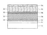
- FIG. 1illustrates a cross sectional view of a substrate with topographical features having various layers disposed thereon.
- this figureillustrates a substrate 2 with or without devices (i.e., transistors, etc.) having deposited thereon a barrier or adhesive layer 4 and a seed layer 6 .
- the top surface of the substrate 2may be patterned with vias, trenches, holes, and other features, or it may be flat.
- the barrier layer 4may be tantalum (Ta), nitrides of tantalum (Ta), titanium (Ti), tungsten, TiW, CuWP, CoWP or combinations of any other material that is commonly used in this field.
- the barrier layer 4is generally deposited on the substrate 2 by any of the various sputtering methods, by chemical vapor deposition (CVD), or by electrolyte/electroless plating methods. Thereafter, the seed layer 6 is deposited over the barrier layer 4 .
- the barrier layer 4 and the seed layer 6may also be formed on the substrate 2 by using an electro-deposition method. This method offers distinct and unique advantages of lower costs and beneficial material properties (i.e., low stress in the substrate 2 ) as opposed to using other deposition methods.
- the seed layer 6 materialmay be copper or copper substitutes.
- the seed layer 6may be deposited on the barrier layer 4 using various sputtering methods, CVD, or electroless deposition or combinations thereof.
- the seed layer 6 thickness, depending on the substrate 2 topography,may vary from 20 to 1500 A°, and may be discontinuous on the corners of the deep recesses of the substrate 2 .
- a conductive layer 8e.g., copper layer is generally electroplated over the seed layer 6 from a suitable acid or non-acidic plating bath or bath formulation.
- the texture of a large portion of the conductive layer 8is dependent upon the texture of an underneath layer, for example, the seed layer 6 .
- Texture as defined in this applicationincludes, but are not limited to, the crystal orientation (i.e., ⁇ 111>, ⁇ 110>), grain size, grain boundary (boundary around a single grain), etc.
- the texture of the remaining portion of the conductive layer 8is dependent upon the chemicals in the plating bath and the deposition rate. In other words, if the crystal orientation of the seed layer 6 is formed predominantly in a ⁇ 111> orientation, then a large portion of the conductive layer 8 will have the same crystal orientation, that being ⁇ 111>. With that being said, the texture of the seed layer 6 is also dependent upon the texture of the barrier layer 4 .
- the conductive layer 8When the plated conductive layer 8 is formed on the seed layer 6 , the conductive layer 8 may be epitaxial with the seed layer 6 up to a thickness of about 3000 A° from the top surface of the seed layer 6 . However, when the thickness of the conductive layer 8 is above 3000 A°, the texture of the portion of the conductive layer 8 above 3000 A° may be dependent upon the nature of the plating bath.
- the grain size of the initially deposited conductive layeris typically about 30 to 100 A°, but can increase in size in the range of 2,000 to 10,000 A° after grain growth at room temperature.
- the final grain size of the conductive layer 8is dependent on the seed layer 6 material, the chemistry of the plating bath, and annealing temperature.
- the texture of the annealed grains in the conductive layer 8is often very similar to the texture of the grains of the seed layer 6 . Thus, it is very difficult to form grains in the conductive layer 8 that are different in their texture from the grains of the seed layer 6 . In addition, it is also difficult to accelerate room temperature grain growth of the conductive layer 8 without changing the texture of the seed layer 6 , bath chemistry and/or temperature.
- the method according to the present inventionincludes the step of plating a conductive layer on the substrate using an anode/pad that rotates in a manner such that the plating solution is continuously applied onto the substrate without the anode/pad making contact with the substrate. Electrical power may be applied to the anode and the substrate during this plating process.
- the anode and the substratemay be momentarily de-energized, and the pad, which may or may not be rotating, is used to polish/rub against a top portion the conductive layer.
- the top portion of the conductive layeris polished during the “cold working” process (e.g., when the anode and substrate are de-energized). This process can be repeated at least several times depending upon the type of the integrated circuit or device to be manufactured. In this manner, the texture of the conductive layer is altered such that a highly desirable conductive layer is formed.
- the apparatus that performs such platingincludes a circular platen having a pad type material attached thereto.
- the platenfurther includes a circular anode plate, where both the platen and the anode plate can rotate about a first axis while the workpiece may also rotate, move side to side, move in an orbital manner, or remain stationary.
- the plating solutioncan be flowed to or through the pad to plate the workpiece surface.
- an apparatus that performs such platingincludes a pad type material mounted on the cylindrical anode that rotates about a first axis.
- the metal from the plating solutioncan be deposited on the workpiece when a potential difference is applied between the workpiece and the anode.
- the padmay make intermittent contact with the workpiece surface after the conductive layer is formed on the substrate.
- the padmay smear, shear, polish/rub a top portion of the conductive layer in a “cold worked” manner such that the texture of the top portion of the conductive layer is altered.
- the present inventionprovides a method of forming an insitu cold worked layer with the deposited material during the deposition process, or alternate forming cold worked and non-cold worked layers on the substrate.
- the present inventionalso provides a method and apparatus for controlling the texture of the deposited conductive layer from the seed layer, bath chemistry, and temperature.
- FIG. 1illustrates a cross sectional view of a substrate having various layers disposed thereon
- FIG. 2illustrates an enlarged cross sectional view of a cathode workpiece and an anode having a pad in accordance with the preferred embodiment of the present invention
- FIGS. 3A-3Eillustrate cross sectional views of a method for forming a highly desirable conductive layer and advantageously affecting the texture of a conductive layer in accordance with the preferred embodiment of the present invention
- FIG. 4Aillustrates a cross sectional view of a wiring structure having a cold worked layer in accordance with the preferred embodiment of the present invention
- FIG. 4Billustrates a cross sectional view of a wiring structure after annealing and polishing a conductive layer in accordance with the preferred embodiment of the present invention
- FIG. 5illustrates a side view of an apparatus in accordance with the first preferred embodiment of the present invention
- FIG. 6illustrates a side view of an apparatus in accordance with the second preferred embodiment of the present invention.
- FIG. 7illustrates a side view of an apparatus in accordance with the third preferred embodiment of the present invention.
- FIG. 8illustrates a side view of an apparatus in accordance with the fourth preferred embodiment of the present invention.
- FIG. 9illustrates a side view of an apparatus in accordance with the fifth preferred embodiment of the present invention.
- FIG. 10illustrates a side view of an apparatus in accordance with the sixth preferred embodiment of the present invention.
- FIGS. 11A-11Dillustrate cylindrical anode-pad arrangements in accordance with the preferred embodiment of the present invention.
- the texture of the plated materialcan be modified to disassociate it from the texture of the underneath layer.
- intermittently rubbing or cold working the plated materialchanges the crystal orientation of the plated material from, for example ⁇ 111> to a more random orientation.
- the present inventioncan be used in the deposition of magnetic or magnetoresistive type films such as those used for magnetic or magnetoresistive sensor and applications.
- magnetic film depositionin a strong magnetic field, the workpiece is stationary, and only the anode rotates. Insitu cold working of the magnetic film such as permalloy during deposition may enhance the preferred orientation in the deposited film, thus greatly enhancing the desirable magnetic properties.
- the present inventioncan be used with any semiconductor workpieces such as a flat panel, magnetic film head, or packaging substrate including lead-tin solder alloys, or lead free solderable alloys. Further, specific processing parameters such as time, temperature, pressure and the like are provided herein, which specific parameters are intended to be explanatory rather than limiting.
- the present inventionfurther describes a method and apparatus for intermittently applying the conductive material to the semiconductor substrate and also intermittently polishing the substrate when a pad type material or other fixed feature is making contact with the workpiece surface.
- the present inventionapplies electrical current having a potential difference between the workpiece and an anode so that the conductive material can be deposited to the workpiece when such current is applied.
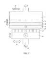
- FIG. 2illustrates an enlarged cross sectional view of a cathode workpiece and an anode having a pad or similar non conductive surface in accordance with the present invention.
- the pad or non conductive surfaceallows an electric field to pass through, but prevents shorting between the anode and the cathode, as described in more detail later herein.
- a barrier layer 14 and a seed layer 16are formed on a workpiece 12 using any known method.
- a first conductive layer 18 of, for example, copperis plated over the seed layer 16 . Copper may be deposited on the seed layer 16 using a highly leveling or non-leveling bath at a current density that ranges from 3 to 70 MA/cm 2 but preferably the current density should be between 5 to 30 MA/cm 2 .
- a proximity plating methodcan be used to form the copper layer 18 on the seed layer 16 .
- An anode 24 having a pad (or a non conductive surface) 22is used during the proximity plating method.
- the spacing or gap 20 between the conductive copper layer 18 and the pad 22may range from less than 1 micron up to 2 millimeter.
- the diameter or cross sectional length of the pad 22 and the workpiece 12may range from about 5 millimeter to over 300 millimeter. The larger the workpiece, the larger the anode diameter.
- the workpiece 12 and the anode 24may be any suitable shape (e.g., circular, spherical, etc.).
- a workpiece head assembly 11is used to hold and position the workpiece 12 .
- the workpiece head assembly 11 having the workpiece 12 , and the anode 24can rotate about their major axis 26 and move vertically as indicated by arrow 30 .
- the rate of rotation for both the workpiece 12 and the anode 24may range from 10 to 2000 rpm and may rotate at a different rate and direction from each other.
- the workpiece 12may be stationary while only the anode 24 rotates.
- the workpiece 12may rotate and/or move vertically while the anode 24 is stationary.
- anode 24 and the workpiece head assembly 11may move laterally (side to side) in the direction indicated by arrow 28 during the deposition process.
- the anode 24 and pad 22may be much larger (i.e., 1.5 to 10 times larger in overall area than the workpiece 12 ) such that multiple workpieces 12 may be plated and polished simultaneously.
- an electrolyte solutionis flowed through or to the pad 22 at a rate between 0.05 to 4 gpm, but preferably between 0.1 to 3 gpm.
- Electrical powermay be applied to the anode 24 and the workpiece 12 during this deposition process.
- coppermay be deposited on the workpiece for 30 to 90 seconds at a suitable current density, after which the pad 22 is brought in contact with the conductive layer (copper) 18 for about 1 to 180 seconds, at a pressure that may range from 0.0001 to about 5 psi. When such contact is made, the conductive layer 18 is cold worked or scratched polished. Electro-deposition may continue during this insitu cold working process.
- the cathode (workpiece) and/or anodeare momentary de-energized during this cold working process.
- a layer of non-cold worked conductive layermay be deposited over the cold worked layer as described above.
- stepssuch as electro-depositing/cold working/electro-depositing can be performed on the workpiece 12 .
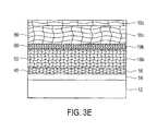
- FIGS. 3A-3Eillustrate cross sectional views of a method for forming a highly desirable conductive layer on a workpiece in accordance with the preferred embodiment of the present invention.
- a barrier layer 14 and a seed layer 16are disposed on a workpiece 12 using any method described above.
- the seed layer 16is composed of individual grains 40 , which are oriented in a predetermined order, such as a ⁇ 111> crystal orientation.
- the grains 40will generally be small, ranging between 20 to 200 A° or higher depending on processing conditions.
- a first conductive layer 18 bis plated on the seed layer 16 using a proximity plating method, or other plating methods.
- the first conductive layer 18 bwill include grains 50 , which will retain most of the crystal orientation of the seed layer 16 . Accordingly, if the grains 40 in the seed layer 16 have a ⁇ 111> crystal orientation, so will most of the grains 50 in the first conductive layer 18 b .
- the size of the grains 40 , 50will also be very similar.
- an abrasive surfacesuch as a pad 22 , polishes/rubs/buffs the first conductive layer 18 b and creates dangling bonds and may change the crystal orientation of the deposited material.
- the padpolishes/rubs the first conductive layer 18 b in a cold worked manner. It has been determined that the polishing action causes the grains in the top portion of the first conductive layer 18 b (cold worked layer) to have a different texture than the underneath layer of the first conductive layer 18 b.
- FIG. 3Cillustrates a cold worked layer 19 b (top portion of the first conductive layer 18 b ).
- the texture of the material in the cold worked layer 19 bwill be significantly different from the texture of the rest of the first conductive layer 18 b .
- the smaller grains 60range between 20 to 80 A°.
- a second level conductive layer 18 cis proximately plated over the first cold worked layer 19 b using the pad 22 .
- the texture of the second conductive layer 18 cwill be different from that of the first conductive layer 18 b , even though both layers are deposited by the proximity plating method.
- the cold worked layer 19 bis used to disassociate the texture of grains 80 of the second conductive layer 18 c from that of the first conductive layer 18 b.
- FIG. 4Aillustrates an enlarged view of a wiring structure having a cold worked layer
- FIG. 4Billustrates an enlarged view of the same wiring structure of FIG. 4A after annealing and polishing the cold worked and conductive layers from the top surface of the substrate.
- a trench 91is formed in an insulating layer 90 using any conventional method.
- a barrier layer 92 and a seed layer 94are then formed on the insulating layer 90 and trench 91 .
- a conductive layer 96is plated on the seed layer 94
- a cold worked layer 98is formed, again using the method described earlier herein.
- the energy stored in the cold worked layer 98is used to accelerate the grain recovery and growth of the deposited conductive layer 96 during an annealing process.
- large grain sizeis obtained in the deposited material at a lower annealing temperature and for a shorter annealing time, as defined below.
- FIG. 4Billustrates the wiring structure after the substrate has been annealed and polished.
- the substratecan be annealed preferably at a temperature between 50 to 400° C. for a period of 15 seconds to 60 minutes.
- the annealing processcan transform the smaller grains 95 to a larger grain 97 , or a single crystal via and line, as illustrated in FIG. 4 B.
- the size of the larger grain 97 formed in the conductive layer 96(copper or gold) is preferably between 1 to 100 microns or larger, as compared to 0.5 to 2 um without using the cold working process.
- the polishing stepmay then be performed using CMP or any other conventional method.
- the inventors of the present inventionhave determined that polishing the substrate is more efficient and effective after cold working and annealing the substrate.
- the seed layer 92 that is shown in FIG. 4Ais formed as part of the grain 97 because of the annealing temperature.
- the larger grain (crystal) 97 in the conductive layer 96provides better electro migration, corrosion resistance, and longer fatigue life than a conductive layer having smaller grains 95 formed as a result of not using the cold working process.
- the conductive material 92 having the larger grain 97forms a single crystal via-line/line-via in the substrate.
- the cold worked layer 98can be considered a sacrificial layer in the substrate because it is used primarily to modify the texture of the conductive layer for better performance.
- FIG. 5illustrates a side view of an apparatus in a first preferred embodiment of the present invention.
- the apparatus 100includes a rotatable platen 102 fixed to a rotatable shaft 104 , a pad 22 a mounted on the platen 102 , and a workpiece head assembly 150 arranged in proximity to the platen 102 .
- the rotatable platen 102 and/or pad 22 amay be circular, pear-shaped, or form in any other shape so long as they can effectively and efficiently plate and cold work the workpiece.
- the head assembly 150 and/or the platen 102are adapted to move up and down when a suitable force is exerted. The force is generated, for example, by mechanical, electromechanical and/or pneumatic means as known in the art.
- a plating solutionis preferably flowed through the platen 102 and the pad 22 a via channel 110 .
- the plating solutionis splashed or applied via pad 22 a onto the workpiece 120 while the cathode/anode electrodes are energized.
- a conductive layeris thus formed on the workpiece 120 .
- the distance between the workpiece 120 and the pad 22 ais less than 1 micron up to 2 millimeters.
- an electrical potentialis applied to the workpiece 120 via contacts 122 .
- a circular anode plate or similar plate type object 118 in the platen 102is used such that an electric potential is applied thereto.
- the plating solution that is flowed via pad 22 aforms a closed circuit.
- thisallows for a more uniform, high quality layer to be formed on the surface of the workpiece 120 .
- either the head assembly 150is lowered and/or the plating apparatus 112 is raised such that the pad type object 22 a makes contact with the workpiece 120 in a cold worked manner.
- the orientation of the various atomic plane in the conductive layeris disoriented/modified.
- the workpiece head assembly 150 and the plating apparatus 112are spaced apart so that a second conductive layer may be formed on the workpiece surface. This process is repeated until a desirable layer is formed.
- the workpiece head assembly 150may include a nonconductive, preferably circular, chuck 152 with a cavity that is preferably a few millimeters deep at its center and which cavity may contain a resting suction pad (not shown).
- the workpiece 120is loaded into the cavity, backside first, against the resting suction pad using a conventional type of transport or vacuum mechanism to ensure that the workpiece 120 is stationary with respect to the head assembly 150 while in use.
- a nonconductive retaining ringsuch as an O-ring or other rubber type of seal at the periphery of the head assembly 150 and a cathode contact electrode 122 each push against the edge of the workpiece 120 and hold it in place.
- the entire back side of the workpiece 120 which pushes against the chuck 152 that is under the retaining ringis thus protected from any and all solutions, including electrolyte.
- Other conventional workpiece head assembliescan be used in accordance with the present invention.
- the electric potentialcan be applied to the wafer using a ring conductor.
- other methods of applying the electric potential to the wafermay be used in accordance with the present invention.
- a liquid conductor or an inflatable tube coated with a conductive materialmay be used in the present invention.
- An example of using the liquid conductor or the conductive tube to provide the necessary electric potential according to the present inventionis disclosed in the co-pending U.S. application Ser. No. 09/283,024, entitled “Method And Apparatus For Forming an Electric Contact With a Semiconductor Substrate”, commonly owned by the assignee of the present invention.
- any known method for providing the electric potentials to the anode 118 and cathode workpiece 120can be used in the present invention. As is known in the art, the difference in the electric potential applied to the anode 118 and workpiece 120 results in the workpiece surface being plated.
- FIG. 6illustrates a second preferred embodiment of the apparatus in accordance with the present invention.
- the workpiece head assembly 150may be the same as that described with reference to FIG. 5 .
- a plating apparatus 170is considerably smaller than the plating apparatus 112 of FIG. 5 , but the features and functionality of the two plating apparatus 112 , 170 are similar.
- the surface of the pad that is attached to the plating apparatus 170is about 30 to 60%, or preferably 45 to 55%, of the workpiece surface.
- the plating apparatus 170may rotate at a rate from 40 to 500 rpm and the workpiece head assembly 150 may rotate at a rate between 30 to 1000 rpm.
- the plating apparatus 170may also move laterally (side to side) in order to plate/cold work the entire workpiece via, for example, rollers (not shown).
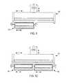
- FIG. 7illustrates a third preferred embodiment in accordance with the present invention.
- two plating apparatus 180 and 190may be used to plate/cold work the workpiece. In other embodiments, more than two plating apparatus may be used simultaneously to plate/cold work the workpiece.
- FIG. 8illustrates a fourth embodiment of the apparatus in accordance with the present invention.
- the anode assembly 200 having a pad 22 b mounted on a cylindrical anode 202may rotate about a first axis 240 , and a workpiece head assembly 150 having a workpiece 120 may rotate about another axis 246 .
- the head assembly 150is similar to that described above with respect to the first embodiment of the present invention.
- the cylindrical anode 202is connected to shafts 208 for rotating about axis 240 . Although shown as operating upon a single workpiece, it is understood that a plurality of head assemblies 150 can be used with the present invention.
- the anode assembly 200is positioned within a chamber 250 that may include a plating solution 260 .
- the apparatusapplies, using a power source, a negative potential to the cathode contact 122 and a positive potential to the anode 202 .
- metal in the plating solution 260is deposited on the surface of the workpiece 120 while the cylindrical anode rotates about axis 240 similar to that described above with reference to FIG. 5 .
- the head assemblyis preferably lowered such that the workpiece 120 can be “cold worked” with the pad 22 b . The plating and “cold worked” steps are repeated until a desirable layer is formed on the workpiece.
- FIG. 9illustrates a fifth preferred embodiment of the apparatus in accordance with the present invention.
- the workpiece head assembly 150may be the same as that described with reference to FIGS. 5-8 .
- a plating chamber 270is considerably smaller than the plating chamber 250 of FIG. 8 , but the features and functionality of the two chambers 250 , 270 are similar.
- the surface of the pad that is attached to the cylindrical anode in the plating chamber 270is about 30 to 60%, or preferably 45 to 55%, of the workpiece surface.
- the cylindrical anode in the plating chamber 270may rotate preferably at a rate from 40 to 500 rpm and the workpiece head assembly 150 may rotate at a rate between 50 to 1000 rpm.
- the plating chamber 270may also move laterally (side to side) in order to plate/cold work the entire workpiece via, for example, rollers (not shown).
- FIG. 10illustrates a sixth preferred embodiment in accordance with the present invention.
- two plating chambers 280 and 290(similar to the plating chamber 270 ) having cylindrical anodes and pads attached thereto may be used to plate/cold work the workpiece.
- more than two plating chambers and/or cylindrical anodes and padsmay be used simultaneously to plate/cold work the workpiece.
- the plating solutioncan be introduced to the pad 22 a , 22 b from a reservoir (not shown) located in proximity to the anodes.
- the anodescan have an in-channel that includes passageways within the center of anodes and holes that are made in the anode which together provide a path for the solution to be fed to the gap between the anode and the cathode.
- the plating solutioncan be dispensed directly onto the pad 22 a , 22 b through another channel in accordance with the methods described earlier herein.
- the pad 22 , 22 a , 22 bis preferably made of a nonconductive, hard, porous or perforated type material such as polyurethane.
- a nonconductive, hard, porous or perforated type materialsuch as polyurethane.
- An example of such padis the IC 1000 pad manufactured by Rodel, Inc.
- the pad 22 , 22 a , 22 bpreferably has a circular shape, but may be shaped in any other form so long as it can effectively plate and/or cold work the workpiece.
- the hardness of the pad 22 , 22 a , 22 b or fixed fixtureis coupled with the relative speed of travel of the pad to the workpiece. In other words, depending on the speed of rotation of the pad and/or the workpiece, the particular pad may be selected with a certain level of hardness.
- the pad materialmay be metallic, which is then separated from the anode by a porous insulating layer.
- the pad 22 , 22 a , 22 bmay also contain fixed abrasives, which may be embedded in or are components of the pad 22 , 22 a , 22 b .
- the particle size of the abrasivesmay range from 50 A° to 50,000 A°, but preferably is within 50 A° to 2000 A°. Also, the standard deviation of the particle size should be fairly low, preferably less than 5% of the mean size of the particles.
- the abrasive materialmay, for example, consist of silica, silicon carbide, boron carbide, carbide particulate, allumina, cerium oxide, zirconia, titanium oxide, diamond, powders, nitride particles (boron nitrides, silicon nitrides, tantalium nitrides, titanium nitrides, and the like) or other various hard particles or their various combinations.
- nitride particlesboron nitrides, silicon nitrides, tantalium nitrides, titanium nitrides, and the like
- the choice of abrasive and pad materials or their combinationshould be such that the abrasives or the pad material are sparingly soluble, preferably insoluble in the electrolyte solution being used.
- the particle contact loading within the pad matrixmay range from 5% to 75%, depending on the nature of the matrix material.
- the matrix material in the padis preferably a polymeric material, such as acid resistant polymers, polyurethanes, highly cross-linked epoxies, highly fluorinated elastomers, kevler and other suitable materials.
- the pad matrix materialmay also be a metallic. In the case of a metallic material, to prevent electrically shorting the workpiece and the anode, it is imperative that a thin porous insulating material isolates the anode from the electrically conductive pad material.
- the pad materialmay be a porous or perforated thin sheet of acid resistant amorphous material, glass, ceramic, or glass-ceramic material.
- perforated thin sheet of alumina or silicon carbidemay be used.
- FIGS. 11A-11Dillustrate different cylindrical anode-pad arrangements in accordance with the preferred embodiment of the present invention.
- the cylindrical anode-pad arrangements described in FIGS. 11A-11Dcan be used in the plating chambers as described and illustrated with reference to FIGS. 8-10 .
- FIG. 11Aillustrates an anode assembly 300 having a cylindrical anode 310 and pad strips 320 that are attached thereto in a longitudinal direction.
- the cylindrical anode 310is further connected to shafts 330 for rotating in a clockwise/counterclockwise direction.
- FIG. 11Balso illustrates an anode assembly 400 having a cylindrical anode 410 and a plurality of circular pads 420 that are attached to the cylindrical anode 410 .
- the cylindrical anode 410is further connected to shafts 430 for rotating in a clockwise/counterclockwise direction.
- FIG. 11Cillustrates an anode assembly 500 having a cylindrical anode 510 and a continuous pad 520 that is attached to the cylindrical anode 410 .
- the continuous padcovers the entire outer surface of the cylindrical anode 510 .
- the cylindrical anode 510is further connected to shafts 530 for rotating in a clockwise/counterclockwise direction.
- FIG. 11Dillustrates an anode assembly 600 having a cylindrical anode 610 and pad strips 620 that are attached to the cylindrical anode 610 in a circular manner.
- the cylindrical anode 610is further connected to shafts 630 for rotating in a clockwise/counterclockwise direction.
- FIGS. 11A-11DEach of the anode-pad arrangements of FIGS. 11A-11D allows for efficient and effective plating and cold working of the workpiece. Although only four anode-pad arrangements are described herein, the present invention can be implemented with different anode-pad arrangements and geometry so long as they can plate and cold worked the workpiece in a similar manner as described herein.
- FIGS. 2-10are shown in a horizontal arrangement parallel to the pad.
- the present inventioncan be implemented such that the workpiece/anode can be positioned in any arbitrary angle with respect to the horizontal plane.
- the workpiece/anodemay be disposed in a vertical arrangement.
- the workpiecemay be mechanically pulsed during the metal deposition step.
- the benefit of the mechanical pulsingis that it improves filling efficiency of the contact holes, vias, and trenches, and copper film integrity without the need for power supplies with pulsing capabilities.
- the workpiecemay be annealed in an inert ambient at a temperature range of 50 to 400° C. for a period of 15 seconds to 60 minutes to initiate massive grain growth.
- CMPis a material planarization process that combines chemical removal of semiconductor layers such as insulators or metals with mechanical buffering of the substrate surface.
- CMPmay provide global planarization of the workpiece surface.
- metal depositionmay occur in any type of plating cell, and after such metal deposition, the workpiece may be transferred to another tool or cell, (i.e. CMP tool), where the deposited metal surface is cold worked.
- CMP toolanother tool or cell, where the deposited metal surface is cold worked.
- plating and cold worked plated metal or materialmay be laminated using more than one tool set, prior to subsequent processes.
- a first cellmay be an electroless plating cell, an electroplating cell, a CVD cell, or a sputtering cell.
- a second cellmay also be a plating cell.
- a different type of materialmay be laminated or sandwiched between conductive layers.
- the workpiecemay be transferred to another cell, where an insulator material or another type of metal or alloy (i.e., PERMALLOY—registered Trademark) may be deposited over the cold worked copper layer.
- the surface of the deposited PERMALLOY (nickel-iron alloy)in turn may be cold worked prior to subsequent depositions or processes.
- a stack of materialsconsisting of, for example, Cu/Ni—Fe/Cu/Ni—Fe/etc., where the Cu and Ni—Fe layer may consist of at least one cold worked surface, is formed prior to subsequent processes.
- the material deposited over the cold worked layerdoes not need to be electro-deposited.
- the new materialcould be deposited by CVD, sputtering, spin coating, immersion plating, electroless plating and the like.
- the cold worked surfaceis copper, it may be coated with, for example, CoP, Au, NiP, from electroless plating bath.
- conductive materialsuch as aluminum, iron, nickel, chromium, indium, lead, tin, lead-tin alloys, nonleaded solderable alloys, silver, zinc, cadmium, titanium, tungsten, molybdenum, ruthenium, their respective alloys and various combinations of above material with oxygen, nitrogen, hydrogen and phosphorous may be used in the present invention.
- conductive materialssuch as aluminum, iron, nickel, chromium, indium, lead, tin, lead-tin alloys, nonleaded solderable alloys, silver, zinc, cadmium, titanium, tungsten, molybdenum, ruthenium, their respective alloys and various combinations of above material with oxygen, nitrogen, hydrogen and phosphorous may be used in the present invention.
- the present inventionmay be used with insulators, such as glasses, and polymeric and nonpolymeric insulators.
- the insulatormay be spin coated, evaporate-deposited or even sputtered, and the insulator is such that its dielectric constant is preferably lower than 4 or higher than 7.
- This present inventionis especially suited for the fabrication of high performance and highly reliable chip interconnect, packaging, magnetic, flat panel and optoelectronic applications. Besides providing a method to control and alter the texture of the conductive layer, the present invention also provides a method of fabricating grain or crystal interconnect structures, such that adjacent (above or under) vias and holes are essentially a single grain or crystal.
Landscapes
- Engineering & Computer Science (AREA)
- Chemical & Material Sciences (AREA)
- Organic Chemistry (AREA)
- Chemical Kinetics & Catalysis (AREA)
- Electrochemistry (AREA)
- Materials Engineering (AREA)
- Metallurgy (AREA)
- Physics & Mathematics (AREA)
- Mechanical Engineering (AREA)
- Condensed Matter Physics & Semiconductors (AREA)
- General Physics & Mathematics (AREA)
- Computer Hardware Design (AREA)
- Microelectronics & Electronic Packaging (AREA)
- Power Engineering (AREA)
- Manufacturing & Machinery (AREA)
- Electroplating Methods And Accessories (AREA)
- Internal Circuitry In Semiconductor Integrated Circuit Devices (AREA)
Abstract
Description
Claims (9)
Priority Applications (3)
| Application Number | Priority Date | Filing Date | Title |
|---|---|---|---|
| US10/165,673US6837979B2 (en) | 1998-12-01 | 2002-06-06 | Method and apparatus for depositing and controlling the texture of a thin film |
| US10/302,755US7204917B2 (en) | 1998-12-01 | 2002-11-21 | Workpiece surface influencing device designs for electrochemical mechanical processing and method of using the same |
| US11/786,948US7670473B1 (en) | 1998-12-01 | 2007-04-12 | Workpiece surface influencing device designs for electrochemical mechanical processing and method of using the same |
Applications Claiming Priority (4)
| Application Number | Priority Date | Filing Date | Title |
|---|---|---|---|
| US09/201,929US6176992B1 (en) | 1998-11-03 | 1998-12-01 | Method and apparatus for electro-chemical mechanical deposition |
| US09/285,621US6328872B1 (en) | 1999-04-03 | 1999-04-03 | Method and apparatus for plating and polishing a semiconductor substrate |
| US09/373,681US6409904B1 (en) | 1998-12-01 | 1999-08-13 | Method and apparatus for depositing and controlling the texture of a thin film |
| US10/165,673US6837979B2 (en) | 1998-12-01 | 2002-06-06 | Method and apparatus for depositing and controlling the texture of a thin film |
Related Parent Applications (1)
| Application Number | Title | Priority Date | Filing Date |
|---|---|---|---|
| US09/373,681DivisionUS6409904B1 (en) | 1998-12-01 | 1999-08-13 | Method and apparatus for depositing and controlling the texture of a thin film |
Related Child Applications (1)
| Application Number | Title | Priority Date | Filing Date |
|---|---|---|---|
| US10/302,755Continuation-In-PartUS7204917B2 (en) | 1998-12-01 | 2002-11-21 | Workpiece surface influencing device designs for electrochemical mechanical processing and method of using the same |
Publications (2)
| Publication Number | Publication Date |
|---|---|
| US20020153256A1 US20020153256A1 (en) | 2002-10-24 |
| US6837979B2true US6837979B2 (en) | 2005-01-04 |
Family
ID=23473415
Family Applications (2)
| Application Number | Title | Priority Date | Filing Date |
|---|---|---|---|
| US09/373,681Expired - Fee RelatedUS6409904B1 (en) | 1998-12-01 | 1999-08-13 | Method and apparatus for depositing and controlling the texture of a thin film |
| US10/165,673Expired - Fee RelatedUS6837979B2 (en) | 1998-12-01 | 2002-06-06 | Method and apparatus for depositing and controlling the texture of a thin film |
Family Applications Before (1)
| Application Number | Title | Priority Date | Filing Date |
|---|---|---|---|
| US09/373,681Expired - Fee RelatedUS6409904B1 (en) | 1998-12-01 | 1999-08-13 | Method and apparatus for depositing and controlling the texture of a thin film |
Country Status (3)
| Country | Link |
|---|---|
| US (2) | US6409904B1 (en) |
| AU (1) | AU7758800A (en) |
| WO (1) | WO2001013416A1 (en) |
Cited By (37)
| Publication number | Priority date | Publication date | Assignee | Title |
|---|---|---|---|---|
| US20070128994A1 (en)* | 2005-12-02 | 2007-06-07 | Chien-Min Sung | Electroplated abrasive tools, methods, and molds |
| US20080250722A1 (en)* | 2007-04-10 | 2008-10-16 | Chien-Min Sung | Electroplated abrasive tools, methods, and molds |
| US20100248596A1 (en)* | 2006-11-16 | 2010-09-30 | Chien-Min Sung | CMP Pad Dressers with Hybridized Abrasive Surface and Related Methods |
| US20110212670A1 (en)* | 2005-09-09 | 2011-09-01 | Chien-Min Sung | Methods of bonding superabrasive particles in an organic matrix |
| US8974270B2 (en) | 2011-05-23 | 2015-03-10 | Chien-Min Sung | CMP pad dresser having leveled tips and associated methods |
| US9011563B2 (en) | 2007-12-06 | 2015-04-21 | Chien-Min Sung | Methods for orienting superabrasive particles on a surface and associated tools |
| US9067301B2 (en) | 2005-05-16 | 2015-06-30 | Chien-Min Sung | CMP pad dressers with hybridized abrasive surface and related methods |
| US9138862B2 (en) | 2011-05-23 | 2015-09-22 | Chien-Min Sung | CMP pad dresser having leveled tips and associated methods |
| US9199357B2 (en) | 1997-04-04 | 2015-12-01 | Chien-Min Sung | Brazed diamond tools and methods for making the same |
| US9221154B2 (en) | 1997-04-04 | 2015-12-29 | Chien-Min Sung | Diamond tools and methods for making the same |
| US9238207B2 (en) | 1997-04-04 | 2016-01-19 | Chien-Min Sung | Brazed diamond tools and methods for making the same |
| US9409280B2 (en) | 1997-04-04 | 2016-08-09 | Chien-Min Sung | Brazed diamond tools and methods for making the same |
| US9463552B2 (en) | 1997-04-04 | 2016-10-11 | Chien-Min Sung | Superbrasvie tools containing uniformly leveled superabrasive particles and associated methods |
| US9475169B2 (en) | 2009-09-29 | 2016-10-25 | Chien-Min Sung | System for evaluating and/or improving performance of a CMP pad dresser |
| US9724802B2 (en) | 2005-05-16 | 2017-08-08 | Chien-Min Sung | CMP pad dressers having leveled tips and associated methods |
| US9868100B2 (en) | 1997-04-04 | 2018-01-16 | Chien-Min Sung | Brazed diamond tools and methods for making the same |
| US10876198B2 (en) | 2015-02-10 | 2020-12-29 | Arcanum Alloys, Inc. | Methods and systems for slurry coating |
| US11011494B2 (en) | 2018-08-31 | 2021-05-18 | Invensas Bonding Technologies, Inc. | Layer structures for making direct metal-to-metal bonds at low temperatures in microelectronics |
| US11152020B1 (en) | 2018-05-14 | 2021-10-19 | Seagate Technology Llc | Electrodeposition of thermally stable alloys |
| US11158573B2 (en) | 2018-10-22 | 2021-10-26 | Invensas Bonding Technologies, Inc. | Interconnect structures |
| US11244920B2 (en) | 2018-12-18 | 2022-02-08 | Invensas Bonding Technologies, Inc. | Method and structures for low temperature device bonding |
| US11261516B2 (en) | 2016-05-20 | 2022-03-01 | Public Joint Stock Company “Severstal” | Methods and systems for coating a steel substrate |
| US11377749B1 (en) | 2017-10-17 | 2022-07-05 | Seagate Technology Llc | Electrodeposition of high damping magnetic alloys |
| US11393779B2 (en) | 2018-06-13 | 2022-07-19 | Invensas Bonding Technologies, Inc. | Large metal pads over TSV |
| US11515279B2 (en) | 2018-04-11 | 2022-11-29 | Adeia Semiconductor Bonding Technologies Inc. | Low temperature bonded structures |
| US11552041B2 (en) | 2017-09-24 | 2023-01-10 | Adeia Semiconductor Bonding Technologies Inc. | Chemical mechanical polishing for hybrid bonding |
| US11710718B2 (en) | 2015-07-10 | 2023-07-25 | Adeia Semiconductor Technologies Llc | Structures and methods for low temperature bonding using nanoparticles |
| US11728313B2 (en) | 2018-06-13 | 2023-08-15 | Adeia Semiconductor Bonding Technologies Inc. | Offset pads over TSV |
| US11735523B2 (en) | 2020-05-19 | 2023-08-22 | Adeia Semiconductor Bonding Technologies Inc. | Laterally unconfined structure |
| US11804377B2 (en) | 2018-04-05 | 2023-10-31 | Adeia Semiconductor Bonding Technologies, Inc. | Method for preparing a surface for direct-bonding |
| US11894326B2 (en) | 2017-03-17 | 2024-02-06 | Adeia Semiconductor Bonding Technologies Inc. | Multi-metal contact structure |
| US11908739B2 (en) | 2017-06-05 | 2024-02-20 | Adeia Semiconductor Technologies Llc | Flat metal features for microelectronics applications |
| US11929347B2 (en) | 2020-10-20 | 2024-03-12 | Adeia Semiconductor Technologies Llc | Mixed exposure for large die |
| US11973056B2 (en) | 2016-10-27 | 2024-04-30 | Adeia Semiconductor Technologies Llc | Methods for low temperature bonding using nanoparticles |
| US12100676B2 (en) | 2018-04-11 | 2024-09-24 | Adeia Semiconductor Bonding Technologies Inc. | Low temperature bonded structures |
| US12211809B2 (en) | 2020-12-30 | 2025-01-28 | Adeia Semiconductor Bonding Technologies Inc. | Structure with conductive feature and method of forming same |
| US12381128B2 (en) | 2020-12-28 | 2025-08-05 | Adeia Semiconductor Bonding Technologies Inc. | Structures with through-substrate vias and methods for forming the same |
Families Citing this family (77)
| Publication number | Priority date | Publication date | Assignee | Title |
|---|---|---|---|---|
| US7449098B1 (en) | 1999-10-05 | 2008-11-11 | Novellus Systems, Inc. | Method for planar electroplating |
| US7531079B1 (en) | 1998-10-26 | 2009-05-12 | Novellus Systems, Inc. | Method and apparatus for uniform electropolishing of damascene IC structures by selective agitation |
| US6409904B1 (en)* | 1998-12-01 | 2002-06-25 | Nutool, Inc. | Method and apparatus for depositing and controlling the texture of a thin film |
| US7204917B2 (en) | 1998-12-01 | 2007-04-17 | Novellus Systems, Inc. | Workpiece surface influencing device designs for electrochemical mechanical processing and method of using the same |
| EP1052062A1 (en)* | 1999-05-03 | 2000-11-15 | Applied Materials, Inc. | Pré-conditioning fixed abrasive articles |
| US6299741B1 (en)* | 1999-11-29 | 2001-10-09 | Applied Materials, Inc. | Advanced electrolytic polish (AEP) assisted metal wafer planarization method and apparatus |
| US6630059B1 (en) | 2000-01-14 | 2003-10-07 | Nutool, Inc. | Workpeice proximity plating apparatus |
| US6991528B2 (en) | 2000-02-17 | 2006-01-31 | Applied Materials, Inc. | Conductive polishing article for electrochemical mechanical polishing |
| US7077721B2 (en) | 2000-02-17 | 2006-07-18 | Applied Materials, Inc. | Pad assembly for electrochemical mechanical processing |
| US7066800B2 (en)* | 2000-02-17 | 2006-06-27 | Applied Materials Inc. | Conductive polishing article for electrochemical mechanical polishing |
| US7303462B2 (en) | 2000-02-17 | 2007-12-04 | Applied Materials, Inc. | Edge bead removal by an electro polishing process |
| US7678245B2 (en) | 2000-02-17 | 2010-03-16 | Applied Materials, Inc. | Method and apparatus for electrochemical mechanical processing |
| US6848970B2 (en)* | 2002-09-16 | 2005-02-01 | Applied Materials, Inc. | Process control in electrochemically assisted planarization |
| US7670468B2 (en) | 2000-02-17 | 2010-03-02 | Applied Materials, Inc. | Contact assembly and method for electrochemical mechanical processing |
| US20040182721A1 (en)* | 2003-03-18 | 2004-09-23 | Applied Materials, Inc. | Process control in electro-chemical mechanical polishing |
| US6962524B2 (en)* | 2000-02-17 | 2005-11-08 | Applied Materials, Inc. | Conductive polishing article for electrochemical mechanical polishing |
| US6991526B2 (en)* | 2002-09-16 | 2006-01-31 | Applied Materials, Inc. | Control of removal profile in electrochemically assisted CMP |
| US7303662B2 (en) | 2000-02-17 | 2007-12-04 | Applied Materials, Inc. | Contacts for electrochemical processing |
| US7059948B2 (en) | 2000-12-22 | 2006-06-13 | Applied Materials | Articles for polishing semiconductor substrates |
| US7374644B2 (en) | 2000-02-17 | 2008-05-20 | Applied Materials, Inc. | Conductive polishing article for electrochemical mechanical polishing |
| US7125477B2 (en) | 2000-02-17 | 2006-10-24 | Applied Materials, Inc. | Contacts for electrochemical processing |
| US6979248B2 (en) | 2002-05-07 | 2005-12-27 | Applied Materials, Inc. | Conductive polishing article for electrochemical mechanical polishing |
| US7029365B2 (en)* | 2000-02-17 | 2006-04-18 | Applied Materials Inc. | Pad assembly for electrochemical mechanical processing |
| US20090020437A1 (en)* | 2000-02-23 | 2009-01-22 | Basol Bulent M | Method and system for controlled material removal by electrochemical polishing |
| WO2001084617A1 (en)* | 2000-04-27 | 2001-11-08 | Nu Tool Inc. | Conductive structure for use in multi-level metallization and process |
| US7253076B1 (en)* | 2000-06-08 | 2007-08-07 | Micron Technologies, Inc. | Methods for forming and integrated circuit structures containing ruthenium and tungsten containing layers |
| US6896776B2 (en)* | 2000-12-18 | 2005-05-24 | Applied Materials Inc. | Method and apparatus for electro-chemical processing |
| US7172497B2 (en)* | 2001-01-05 | 2007-02-06 | Asm Nutool, Inc. | Fabrication of semiconductor interconnect structures |
| US7344432B2 (en) | 2001-04-24 | 2008-03-18 | Applied Materials, Inc. | Conductive pad with ion exchange membrane for electrochemical mechanical polishing |
| US7137879B2 (en) | 2001-04-24 | 2006-11-21 | Applied Materials, Inc. | Conductive polishing article for electrochemical mechanical polishing |
| JP3963661B2 (en)* | 2001-05-10 | 2007-08-22 | 株式会社荏原製作所 | Electroless plating method and apparatus |
| US7238092B2 (en) | 2001-09-28 | 2007-07-03 | Novellus Systems, Inc. | Low-force electrochemical mechanical processing method and apparatus |
| US20030072639A1 (en)* | 2001-10-17 | 2003-04-17 | Applied Materials, Inc. | Substrate support |
| US6916398B2 (en)* | 2001-10-26 | 2005-07-12 | Applied Materials, Inc. | Gas delivery apparatus and method for atomic layer deposition |
| US6815354B2 (en)* | 2001-10-27 | 2004-11-09 | Nutool, Inc. | Method and structure for thru-mask contact electrodeposition |
| US6837983B2 (en)* | 2002-01-22 | 2005-01-04 | Applied Materials, Inc. | Endpoint detection for electro chemical mechanical polishing and electropolishing processes |
| US20030146102A1 (en)* | 2002-02-05 | 2003-08-07 | Applied Materials, Inc. | Method for forming copper interconnects |
| US20030188975A1 (en)* | 2002-04-05 | 2003-10-09 | Nielsen Thomas D. | Copper anode for semiconductor interconnects |
| US20040072445A1 (en)* | 2002-07-11 | 2004-04-15 | Applied Materials, Inc. | Effective method to improve surface finish in electrochemically assisted CMP |
| US7799200B1 (en) | 2002-07-29 | 2010-09-21 | Novellus Systems, Inc. | Selective electrochemical accelerator removal |
| US20050061674A1 (en)* | 2002-09-16 | 2005-03-24 | Yan Wang | Endpoint compensation in electroprocessing |
| US7112270B2 (en)* | 2002-09-16 | 2006-09-26 | Applied Materials, Inc. | Algorithm for real-time process control of electro-polishing |
| US7138039B2 (en)* | 2003-01-21 | 2006-11-21 | Applied Materials, Inc. | Liquid isolation of contact rings |
| US7087144B2 (en)* | 2003-01-31 | 2006-08-08 | Applied Materials, Inc. | Contact ring with embedded flexible contacts |
| US7025861B2 (en)* | 2003-02-06 | 2006-04-11 | Applied Materials | Contact plating apparatus |
| US7842169B2 (en) | 2003-03-04 | 2010-11-30 | Applied Materials, Inc. | Method and apparatus for local polishing control |
| US6893328B2 (en)* | 2003-04-23 | 2005-05-17 | Rohm And Haas Electronic Materials Cmp Holdings, Inc. | Conductive polishing pad with anode and cathode |
| US20050016861A1 (en)* | 2003-07-24 | 2005-01-27 | Thomas Laursen | Method for planarizing a work piece |
| US8158532B2 (en)* | 2003-10-20 | 2012-04-17 | Novellus Systems, Inc. | Topography reduction and control by selective accelerator removal |
| US8530359B2 (en) | 2003-10-20 | 2013-09-10 | Novellus Systems, Inc. | Modulated metal removal using localized wet etching |
| US20050121141A1 (en)* | 2003-11-13 | 2005-06-09 | Manens Antoine P. | Real time process control for a polishing process |
| US7186164B2 (en)* | 2003-12-03 | 2007-03-06 | Applied Materials, Inc. | Processing pad assembly with zone control |
| US7390744B2 (en) | 2004-01-29 | 2008-06-24 | Applied Materials, Inc. | Method and composition for polishing a substrate |
| US20050218000A1 (en)* | 2004-04-06 | 2005-10-06 | Applied Materials, Inc. | Conditioning of contact leads for metal plating systems |
| US7285195B2 (en)* | 2004-06-24 | 2007-10-23 | Applied Materials, Inc. | Electric field reducing thrust plate |
| US7563348B2 (en)* | 2004-06-28 | 2009-07-21 | Lam Research Corporation | Electroplating head and method for operating the same |
| US7084064B2 (en) | 2004-09-14 | 2006-08-01 | Applied Materials, Inc. | Full sequence metal and barrier layer electrochemical mechanical processing |
| US7520968B2 (en) | 2004-10-05 | 2009-04-21 | Applied Materials, Inc. | Conductive pad design modification for better wafer-pad contact |
| US7655565B2 (en)* | 2005-01-26 | 2010-02-02 | Applied Materials, Inc. | Electroprocessing profile control |
| US7427340B2 (en) | 2005-04-08 | 2008-09-23 | Applied Materials, Inc. | Conductive pad |
| US20070014958A1 (en)* | 2005-07-08 | 2007-01-18 | Chaplin Ernest R | Hanger labels, label assemblies and methods for forming the same |
| US20070153453A1 (en)* | 2006-01-05 | 2007-07-05 | Applied Materials, Inc. | Fully conductive pad for electrochemical mechanical processing |
| US20070235344A1 (en)* | 2006-04-06 | 2007-10-11 | Applied Materials, Inc. | Process for high copper removal rate with good planarization and surface finish |
| US20070251832A1 (en)* | 2006-04-27 | 2007-11-01 | Applied Materials, Inc. | Method and apparatus for electrochemical mechanical polishing of cu with higher liner velocity for better surface finish and higher removal rate during clearance |
| US7422982B2 (en)* | 2006-07-07 | 2008-09-09 | Applied Materials, Inc. | Method and apparatus for electroprocessing a substrate with edge profile control |
| US8012000B2 (en)* | 2007-04-02 | 2011-09-06 | Applied Materials, Inc. | Extended pad life for ECMP and barrier removal |
| US9005420B2 (en)* | 2007-12-20 | 2015-04-14 | Integran Technologies Inc. | Variable property electrodepositing of metallic structures |
| DE102009007992A1 (en)* | 2009-02-07 | 2010-08-19 | Ab Skf | Coating arrangement comprises a coating carrier and a layer arranged on surface of the carrier, where the layer is formed by coating of particles in quasi manner and is fixed with galvanically applied metallic materials on the surface |
| US8168540B1 (en) | 2009-12-29 | 2012-05-01 | Novellus Systems, Inc. | Methods and apparatus for depositing copper on tungsten |
| US20140042030A1 (en)* | 2012-08-10 | 2014-02-13 | General Electric Company | Sealed laminated structure, system and method for electrolytic processing the same |
| US9393759B2 (en) | 2013-10-24 | 2016-07-19 | General Electric Company | Metal laminate structures with systems and methods for treating |
| CN103936108B (en)* | 2014-04-12 | 2015-11-18 | 大连双迪创新科技研究院有限公司 | Bath water device for making |
| CN104120454B (en)* | 2014-07-01 | 2016-08-17 | 湖南创元铝业有限公司 | Prebaked anode non-oxidizability ceramic base coating and painting method thereof |
| CN104532313B (en)* | 2014-12-16 | 2017-03-01 | 广西大学 | Brush Plating experimental machine |
| CN104532314B (en)* | 2014-12-16 | 2017-06-16 | 广西大学 | Connecting rod electric brushing coating installation |
| CN109811310B (en)* | 2019-01-21 | 2020-09-01 | 河南工学院 | Non-ferromagnetic, high-strength and strong-cube-texture nickel-tungsten composite baseband and preparation method thereof |
| CN109989081B (en)* | 2019-04-17 | 2021-05-25 | 浙江宏途电气科技有限公司 | Easy-to-operate brush-plated workpiece repair device |
Citations (31)
| Publication number | Priority date | Publication date | Assignee | Title |
|---|---|---|---|---|
| US3395092A (en) | 1965-05-24 | 1968-07-30 | Ribes Vincent | Dressing apparatus for diamond wheels |
| US3436259A (en) | 1966-05-12 | 1969-04-01 | Ibm | Method for plating and polishing a silicon planar surface |
| DE2008664A1 (en) | 1970-02-25 | 1971-09-09 | Licentia Gmbh | Galvanically or chemically assisted mechanic |
| US3890746A (en) | 1973-09-07 | 1975-06-24 | Kyuji Saegusa | Flapper wheel |
| US3922207A (en) | 1974-05-31 | 1975-11-25 | United Technologies Corp | Method for plating articles with particles in a metal matrix |
| US3959089A (en) | 1972-07-31 | 1976-05-25 | Watts John Dawson | Surface finishing and plating method |
| US4610772A (en) | 1985-07-22 | 1986-09-09 | The Carolinch Company | Electrolytic plating apparatus |
| DE3840310A1 (en) | 1987-12-24 | 1989-07-06 | Bbc Brown Boveri & Cie | Method for accelerated deposition of a thick reconditioning layer on a worn workpiece |
| US5024735A (en) | 1989-02-15 | 1991-06-18 | Kadija Igor V | Method and apparatus for manufacturing interconnects with fine lines and spacing |
| US5171412A (en) | 1991-08-23 | 1992-12-15 | Applied Materials, Inc. | Material deposition method for integrated circuit manufacturing |
| US5272111A (en) | 1991-02-05 | 1993-12-21 | Mitsubishi Denki Kabushiki Kaisha | Method for manufacturing semiconductor device contact |
| DE4324330A1 (en) | 1992-08-01 | 1994-02-03 | Atotech Deutschland Gmbh | Process for the electrolytic treatment of, in particular, flat items to be treated, and arrangement, in particular for carrying out the process |
| WO1995000295A1 (en) | 1993-06-17 | 1995-01-05 | Minnesota Mining And Manufacturing Company | Patterned abrading articles and methods making and using same |
| US5429733A (en) | 1992-05-21 | 1995-07-04 | Electroplating Engineers Of Japan, Ltd. | Plating device for wafer |
| US5558568A (en) | 1994-10-11 | 1996-09-24 | Ontrak Systems, Inc. | Wafer polishing machine with fluid bearings |
| WO1997013009A1 (en) | 1995-09-30 | 1997-04-10 | Zhiwei Du | Method and apparatus for processing of precision parts by using electrolyte |
| US5650039A (en) | 1994-03-02 | 1997-07-22 | Applied Materials, Inc. | Chemical mechanical polishing apparatus with improved slurry distribution |
| US5692947A (en) | 1994-08-09 | 1997-12-02 | Ontrak Systems, Inc. | Linear polisher and method for semiconductor wafer planarization |
| US5755859A (en) | 1995-08-24 | 1998-05-26 | International Business Machines Corporation | Cobalt-tin alloys and their applications for devices, chip interconnections and packaging |
| US5807165A (en) | 1997-03-26 | 1998-09-15 | International Business Machines Corporation | Method of electrochemical mechanical planarization |
| US5833820A (en) | 1997-06-19 | 1998-11-10 | Advanced Micro Devices, Inc. | Electroplating apparatus |
| US5863412A (en) | 1995-10-17 | 1999-01-26 | Canon Kabushiki Kaisha | Etching method and process for producing a semiconductor element using said etching method |
| EP0903774A2 (en) | 1997-09-17 | 1999-03-24 | Ebara Corporation | Substrate plating apparatus |
| WO1999025004A1 (en) | 1997-11-10 | 1999-05-20 | Applied Materials, Inc. | Integrated manufacturing tool comprising electroplating, chemical-mechanical polishing, clean and dry stations, and method therefor |
| US5930669A (en) | 1997-04-03 | 1999-07-27 | International Business Machines Corporation | Continuous highly conductive metal wiring structures and method for fabricating the same |
| US5933753A (en) | 1996-12-16 | 1999-08-03 | International Business Machines Corporation | Open-bottomed via liner structure and method for fabricating same |
| EP0960693A2 (en) | 1998-05-28 | 1999-12-01 | Speedfam Co., Ltd. | A polishing machine |
| US6004880A (en) | 1998-02-20 | 1999-12-21 | Lsi Logic Corporation | Method of single step damascene process for deposition and global planarization |
| US6176992B1 (en) | 1998-11-03 | 2001-01-23 | Nutool, Inc. | Method and apparatus for electro-chemical mechanical deposition |
| US6242349B1 (en)* | 1998-12-09 | 2001-06-05 | Advanced Micro Devices, Inc. | Method of forming copper/copper alloy interconnection with reduced electromigration |
| US6409904B1 (en)* | 1998-12-01 | 2002-06-25 | Nutool, Inc. | Method and apparatus for depositing and controlling the texture of a thin film |
- 1999
- 1999-08-13USUS09/373,681patent/US6409904B1/ennot_activeExpired - Fee Related
- 2000
- 2000-08-09WOPCT/US2000/040626patent/WO2001013416A1/enactiveApplication Filing
- 2000-08-09AUAU77588/00Apatent/AU7758800A/ennot_activeAbandoned
- 2002
- 2002-06-06USUS10/165,673patent/US6837979B2/ennot_activeExpired - Fee Related
Patent Citations (32)
| Publication number | Priority date | Publication date | Assignee | Title |
|---|---|---|---|---|
| US3395092A (en) | 1965-05-24 | 1968-07-30 | Ribes Vincent | Dressing apparatus for diamond wheels |
| US3436259A (en) | 1966-05-12 | 1969-04-01 | Ibm | Method for plating and polishing a silicon planar surface |
| DE2008664A1 (en) | 1970-02-25 | 1971-09-09 | Licentia Gmbh | Galvanically or chemically assisted mechanic |
| US3959089A (en) | 1972-07-31 | 1976-05-25 | Watts John Dawson | Surface finishing and plating method |
| US3890746A (en) | 1973-09-07 | 1975-06-24 | Kyuji Saegusa | Flapper wheel |
| US3922207A (en) | 1974-05-31 | 1975-11-25 | United Technologies Corp | Method for plating articles with particles in a metal matrix |
| US4610772A (en) | 1985-07-22 | 1986-09-09 | The Carolinch Company | Electrolytic plating apparatus |
| DE3840310A1 (en) | 1987-12-24 | 1989-07-06 | Bbc Brown Boveri & Cie | Method for accelerated deposition of a thick reconditioning layer on a worn workpiece |
| US5024735A (en) | 1989-02-15 | 1991-06-18 | Kadija Igor V | Method and apparatus for manufacturing interconnects with fine lines and spacing |
| US5272111A (en) | 1991-02-05 | 1993-12-21 | Mitsubishi Denki Kabushiki Kaisha | Method for manufacturing semiconductor device contact |
| US5171412A (en) | 1991-08-23 | 1992-12-15 | Applied Materials, Inc. | Material deposition method for integrated circuit manufacturing |
| US5429733A (en) | 1992-05-21 | 1995-07-04 | Electroplating Engineers Of Japan, Ltd. | Plating device for wafer |
| DE4324330A1 (en) | 1992-08-01 | 1994-02-03 | Atotech Deutschland Gmbh | Process for the electrolytic treatment of, in particular, flat items to be treated, and arrangement, in particular for carrying out the process |
| WO1995000295A1 (en) | 1993-06-17 | 1995-01-05 | Minnesota Mining And Manufacturing Company | Patterned abrading articles and methods making and using same |
| US5650039A (en) | 1994-03-02 | 1997-07-22 | Applied Materials, Inc. | Chemical mechanical polishing apparatus with improved slurry distribution |
| US5692947A (en) | 1994-08-09 | 1997-12-02 | Ontrak Systems, Inc. | Linear polisher and method for semiconductor wafer planarization |
| US5558568A (en) | 1994-10-11 | 1996-09-24 | Ontrak Systems, Inc. | Wafer polishing machine with fluid bearings |
| US5755859A (en) | 1995-08-24 | 1998-05-26 | International Business Machines Corporation | Cobalt-tin alloys and their applications for devices, chip interconnections and packaging |
| WO1997013009A1 (en) | 1995-09-30 | 1997-04-10 | Zhiwei Du | Method and apparatus for processing of precision parts by using electrolyte |
| US5863412A (en) | 1995-10-17 | 1999-01-26 | Canon Kabushiki Kaisha | Etching method and process for producing a semiconductor element using said etching method |
| US5933753A (en) | 1996-12-16 | 1999-08-03 | International Business Machines Corporation | Open-bottomed via liner structure and method for fabricating same |
| US5807165A (en) | 1997-03-26 | 1998-09-15 | International Business Machines Corporation | Method of electrochemical mechanical planarization |
| US5930669A (en) | 1997-04-03 | 1999-07-27 | International Business Machines Corporation | Continuous highly conductive metal wiring structures and method for fabricating the same |
| US5833820A (en) | 1997-06-19 | 1998-11-10 | Advanced Micro Devices, Inc. | Electroplating apparatus |
| EP0903774A2 (en) | 1997-09-17 | 1999-03-24 | Ebara Corporation | Substrate plating apparatus |
| WO1999025004A1 (en) | 1997-11-10 | 1999-05-20 | Applied Materials, Inc. | Integrated manufacturing tool comprising electroplating, chemical-mechanical polishing, clean and dry stations, and method therefor |
| US6110011A (en)* | 1997-11-10 | 2000-08-29 | Applied Materials, Inc. | Integrated electrodeposition and chemical-mechanical polishing tool |
| US6004880A (en) | 1998-02-20 | 1999-12-21 | Lsi Logic Corporation | Method of single step damascene process for deposition and global planarization |
| EP0960693A2 (en) | 1998-05-28 | 1999-12-01 | Speedfam Co., Ltd. | A polishing machine |
| US6176992B1 (en) | 1998-11-03 | 2001-01-23 | Nutool, Inc. | Method and apparatus for electro-chemical mechanical deposition |
| US6409904B1 (en)* | 1998-12-01 | 2002-06-25 | Nutool, Inc. | Method and apparatus for depositing and controlling the texture of a thin film |
| US6242349B1 (en)* | 1998-12-09 | 2001-06-05 | Advanced Micro Devices, Inc. | Method of forming copper/copper alloy interconnection with reduced electromigration |
Non-Patent Citations (5)
| Title |
|---|
| Alan C. West, et al., "Pulse Reverse Copper Electrodeposition in High Aspect Ration Trenches and Vias", Sep. 1998, pp. 3070-3073. |
| C. Madore, et al., "Blocking Inhibitors in Catholic Leveling", I. "Theoretical Analysis", Dec. 1996, pp. 3927-3942. |
| J.M. Steigerwald, et al., "Pattern Geometry Effects in the Chemical-Mechanical Polishing of Inlaid Copper Structures", Oct. 1994, pp. 2842-2848. |
| M. Rubinstein, "Tampongalvanisieren in der Praxis, Teil 1." GALVANOTECHNIK, vol. 79, No. 10, 1988, pp. 3263-3270. |
| Robert C. Contolini, et al., "Electrochemical Planarization for Multilevel Metallization", Sep. 1994, pp. 2503-2510. |
Cited By (54)
| Publication number | Priority date | Publication date | Assignee | Title |
|---|---|---|---|---|
| US9199357B2 (en) | 1997-04-04 | 2015-12-01 | Chien-Min Sung | Brazed diamond tools and methods for making the same |
| US9868100B2 (en) | 1997-04-04 | 2018-01-16 | Chien-Min Sung | Brazed diamond tools and methods for making the same |
| US9463552B2 (en) | 1997-04-04 | 2016-10-11 | Chien-Min Sung | Superbrasvie tools containing uniformly leveled superabrasive particles and associated methods |
| US9409280B2 (en) | 1997-04-04 | 2016-08-09 | Chien-Min Sung | Brazed diamond tools and methods for making the same |
| US9238207B2 (en) | 1997-04-04 | 2016-01-19 | Chien-Min Sung | Brazed diamond tools and methods for making the same |
| US9221154B2 (en) | 1997-04-04 | 2015-12-29 | Chien-Min Sung | Diamond tools and methods for making the same |
| US9724802B2 (en) | 2005-05-16 | 2017-08-08 | Chien-Min Sung | CMP pad dressers having leveled tips and associated methods |
| US9067301B2 (en) | 2005-05-16 | 2015-06-30 | Chien-Min Sung | CMP pad dressers with hybridized abrasive surface and related methods |
| US20110212670A1 (en)* | 2005-09-09 | 2011-09-01 | Chien-Min Sung | Methods of bonding superabrasive particles in an organic matrix |
| US20070128994A1 (en)* | 2005-12-02 | 2007-06-07 | Chien-Min Sung | Electroplated abrasive tools, methods, and molds |
| US20100248596A1 (en)* | 2006-11-16 | 2010-09-30 | Chien-Min Sung | CMP Pad Dressers with Hybridized Abrasive Surface and Related Methods |
| US8622787B2 (en) | 2006-11-16 | 2014-01-07 | Chien-Min Sung | CMP pad dressers with hybridized abrasive surface and related methods |
| US20080250722A1 (en)* | 2007-04-10 | 2008-10-16 | Chien-Min Sung | Electroplated abrasive tools, methods, and molds |
| US9011563B2 (en) | 2007-12-06 | 2015-04-21 | Chien-Min Sung | Methods for orienting superabrasive particles on a surface and associated tools |
| US9475169B2 (en) | 2009-09-29 | 2016-10-25 | Chien-Min Sung | System for evaluating and/or improving performance of a CMP pad dresser |
| US8974270B2 (en) | 2011-05-23 | 2015-03-10 | Chien-Min Sung | CMP pad dresser having leveled tips and associated methods |
| US9138862B2 (en) | 2011-05-23 | 2015-09-22 | Chien-Min Sung | CMP pad dresser having leveled tips and associated methods |
| US10876198B2 (en) | 2015-02-10 | 2020-12-29 | Arcanum Alloys, Inc. | Methods and systems for slurry coating |
| US11710718B2 (en) | 2015-07-10 | 2023-07-25 | Adeia Semiconductor Technologies Llc | Structures and methods for low temperature bonding using nanoparticles |
| US11261516B2 (en) | 2016-05-20 | 2022-03-01 | Public Joint Stock Company “Severstal” | Methods and systems for coating a steel substrate |
| US12027487B2 (en) | 2016-10-27 | 2024-07-02 | Adeia Semiconductor Technologies Llc | Structures for low temperature bonding using nanoparticles |
| US11973056B2 (en) | 2016-10-27 | 2024-04-30 | Adeia Semiconductor Technologies Llc | Methods for low temperature bonding using nanoparticles |
| US11894326B2 (en) | 2017-03-17 | 2024-02-06 | Adeia Semiconductor Bonding Technologies Inc. | Multi-metal contact structure |
| US11908739B2 (en) | 2017-06-05 | 2024-02-20 | Adeia Semiconductor Technologies Llc | Flat metal features for microelectronics applications |
| US12381173B2 (en) | 2017-09-24 | 2025-08-05 | Adeia Semiconductor Bonding Technologies Inc. | Direct hybrid bonding of substrates having microelectronic components with different profiles and/or pitches at the bonding interface |
| US11552041B2 (en) | 2017-09-24 | 2023-01-10 | Adeia Semiconductor Bonding Technologies Inc. | Chemical mechanical polishing for hybrid bonding |
| US11377749B1 (en) | 2017-10-17 | 2022-07-05 | Seagate Technology Llc | Electrodeposition of high damping magnetic alloys |
| US11913130B1 (en) | 2017-10-17 | 2024-02-27 | Seagate Technology Llc | Electrodeposition of high damping magnetic alloys |
| US11804377B2 (en) | 2018-04-05 | 2023-10-31 | Adeia Semiconductor Bonding Technologies, Inc. | Method for preparing a surface for direct-bonding |
| US12341018B2 (en) | 2018-04-05 | 2025-06-24 | Adeia Semiconductor Bonding Technologies Inc. | Method for preparing a surface for direct-bonding |
| US12046571B2 (en) | 2018-04-11 | 2024-07-23 | Adeia Semiconductor Bonding Technologies Inc. | Low temperature bonded structures |
| US12132020B2 (en) | 2018-04-11 | 2024-10-29 | Adeia Semiconductor Bonding Technologies Inc. | Low temperature bonded structures |
| US12100676B2 (en) | 2018-04-11 | 2024-09-24 | Adeia Semiconductor Bonding Technologies Inc. | Low temperature bonded structures |
| US11515279B2 (en) | 2018-04-11 | 2022-11-29 | Adeia Semiconductor Bonding Technologies Inc. | Low temperature bonded structures |
| US11152020B1 (en) | 2018-05-14 | 2021-10-19 | Seagate Technology Llc | Electrodeposition of thermally stable alloys |
| US11798583B1 (en) | 2018-05-14 | 2023-10-24 | Seagate Technology Llc | Electrodeposition of thermally stable alloys |
| US11728313B2 (en) | 2018-06-13 | 2023-08-15 | Adeia Semiconductor Bonding Technologies Inc. | Offset pads over TSV |
| US11955445B2 (en) | 2018-06-13 | 2024-04-09 | Adeia Semiconductor Bonding Technologies Inc. | Metal pads over TSV |
| US11393779B2 (en) | 2018-06-13 | 2022-07-19 | Invensas Bonding Technologies, Inc. | Large metal pads over TSV |
| US12243851B2 (en) | 2018-06-13 | 2025-03-04 | Adeia Semiconductor Bonding Technologies Inc. | Offset pads over TSV |
| US11749645B2 (en) | 2018-06-13 | 2023-09-05 | Adeia Semiconductor Bonding Technologies Inc. | TSV as pad |
| US12205926B2 (en) | 2018-06-13 | 2025-01-21 | Adeia Semiconductor Bonding Technologies Inc. | TSV as pad |
| US11011494B2 (en) | 2018-08-31 | 2021-05-18 | Invensas Bonding Technologies, Inc. | Layer structures for making direct metal-to-metal bonds at low temperatures in microelectronics |
| US12136605B2 (en) | 2018-08-31 | 2024-11-05 | Adeia Semiconductor Bonding Technologies Inc. | Layer structures for making direct metal-to-metal bonds at low temperatures in microelectronics and method for forming the same |
| US11756880B2 (en) | 2018-10-22 | 2023-09-12 | Adeia Semiconductor Bonding Technologies Inc. | Interconnect structures |
| US11158573B2 (en) | 2018-10-22 | 2021-10-26 | Invensas Bonding Technologies, Inc. | Interconnect structures |
| US12125784B2 (en) | 2018-10-22 | 2024-10-22 | Adeia Semiconductor Bonding Technologies Inc. | Interconnect structures |
| US11244920B2 (en) | 2018-12-18 | 2022-02-08 | Invensas Bonding Technologies, Inc. | Method and structures for low temperature device bonding |
| US12154880B2 (en) | 2018-12-18 | 2024-11-26 | Adeia Semiconductor Bonding Technologies Inc. | Method and structures for low temperature device bonding |
| US11735523B2 (en) | 2020-05-19 | 2023-08-22 | Adeia Semiconductor Bonding Technologies Inc. | Laterally unconfined structure |
| US12033943B2 (en) | 2020-05-19 | 2024-07-09 | Adeia Semiconductor Bonding Technologies Inc. | Laterally unconfined structure |
| US11929347B2 (en) | 2020-10-20 | 2024-03-12 | Adeia Semiconductor Technologies Llc | Mixed exposure for large die |
| US12381128B2 (en) | 2020-12-28 | 2025-08-05 | Adeia Semiconductor Bonding Technologies Inc. | Structures with through-substrate vias and methods for forming the same |
| US12211809B2 (en) | 2020-12-30 | 2025-01-28 | Adeia Semiconductor Bonding Technologies Inc. | Structure with conductive feature and method of forming same |
Also Published As
| Publication number | Publication date |
|---|---|
| AU7758800A (en) | 2001-03-13 |
| US6409904B1 (en) | 2002-06-25 |
| WO2001013416A1 (en) | 2001-02-22 |
| US20020153256A1 (en) | 2002-10-24 |
Similar Documents
| Publication | Publication Date | Title |
|---|---|---|
| US6837979B2 (en) | Method and apparatus for depositing and controlling the texture of a thin film | |
| US7341649B2 (en) | Apparatus for electroprocessing a workpiece surface | |
| US7311811B2 (en) | Device providing electrical contact to the surface of a semiconductor workpiece during processing | |
| US6848977B1 (en) | Polishing pad for electrochemical mechanical polishing | |
| US7572354B2 (en) | Electrochemical processing of conductive surface | |
| US6176992B1 (en) | Method and apparatus for electro-chemical mechanical deposition | |
| US7077725B2 (en) | Advanced electrolytic polish (AEP) assisted metal wafer planarization method and apparatus | |
| US7309406B2 (en) | Method and apparatus for plating and polishing semiconductor substrate | |
| US6852630B2 (en) | Electroetching process and system | |
| US20030064669A1 (en) | Low-force electrochemical mechanical processing method and apparatus | |
| WO2001088954A2 (en) | Method of and apparatus for making electrical contact to wafer surface for full-face electroplating or electropolishing | |
| US6852208B2 (en) | Method and apparatus for full surface electrotreating of a wafer | |
| US7201828B2 (en) | Planar plating apparatus | |
| JP2007511095A (en) | Integrated circuit interconnect fabrication system and method | |
| US6863794B2 (en) | Method and apparatus for forming metal layers | |
| US20050101138A1 (en) | System and method for applying constant pressure during electroplating and electropolishing | |
| KR20050009990A (en) | Polishing method, polishing device, and method of manufacturing semiconductor equipment | |
| JP2005509092A (en) | Electrochemical mechanical processing using an advanceable sweeper | |
| JP2003326419A (en) | Plating method, plating device, and polishing method, polishing device, and method for manufacturing semiconductor device |
Legal Events
| Date | Code | Title | Description |
|---|---|---|---|
| FEPP | Fee payment procedure | Free format text:PAYOR NUMBER ASSIGNED (ORIGINAL EVENT CODE: ASPN); ENTITY STATUS OF PATENT OWNER: LARGE ENTITY | |
| AS | Assignment | Owner name:ASM NUTOOL, INC., CALIFORNIA Free format text:CHANGE OF NAME;ASSIGNOR:NUTOOL, INC.;REEL/FRAME:015748/0065 Effective date:20040729 | |
| AS | Assignment | Owner name:NOVELLUS SYSTEMS, INC.,CALIFORNIA Free format text:ASSIGNMENT OF ASSIGNORS INTEREST;ASSIGNOR:ASM NUTOOL, INC.;REEL/FRAME:019000/0080 Effective date:20061204 Owner name:NOVELLUS SYSTEMS, INC., CALIFORNIA Free format text:ASSIGNMENT OF ASSIGNORS INTEREST;ASSIGNOR:ASM NUTOOL, INC.;REEL/FRAME:019000/0080 Effective date:20061204 | |
| FEPP | Fee payment procedure | Free format text:PAYER NUMBER DE-ASSIGNED (ORIGINAL EVENT CODE: RMPN); ENTITY STATUS OF PATENT OWNER: LARGE ENTITY Free format text:PAYOR NUMBER ASSIGNED (ORIGINAL EVENT CODE: ASPN); ENTITY STATUS OF PATENT OWNER: LARGE ENTITY | |
| FPAY | Fee payment | Year of fee payment:4 | |
| REMI | Maintenance fee reminder mailed | ||
| FEPP | Fee payment procedure | Free format text:PAYER NUMBER DE-ASSIGNED (ORIGINAL EVENT CODE: RMPN); ENTITY STATUS OF PATENT OWNER: LARGE ENTITY Free format text:PAYOR NUMBER ASSIGNED (ORIGINAL EVENT CODE: ASPN); ENTITY STATUS OF PATENT OWNER: LARGE ENTITY | |
| FPAY | Fee payment | Year of fee payment:8 | |
| REMI | Maintenance fee reminder mailed | ||
| LAPS | Lapse for failure to pay maintenance fees | ||
| STCH | Information on status: patent discontinuation | Free format text:PATENT EXPIRED DUE TO NONPAYMENT OF MAINTENANCE FEES UNDER 37 CFR 1.362 | |
| FP | Lapsed due to failure to pay maintenance fee | Effective date:20170104 |