US6836020B2 - Electrical through wafer interconnects - Google Patents
Electrical through wafer interconnectsDownload PDFInfo
- Publication number
- US6836020B2 US6836020B2US10/349,597US34959703AUS6836020B2US 6836020 B2US6836020 B2US 6836020B2US 34959703 AUS34959703 AUS 34959703AUS 6836020 B2US6836020 B2US 6836020B2
- Authority
- US
- United States
- Prior art keywords
- wafer
- junction
- conductor
- front side
- back side
- Prior art date
- Legal status (The legal status is an assumption and is not a legal conclusion. Google has not performed a legal analysis and makes no representation as to the accuracy of the status listed.)
- Expired - Lifetime
Links
- 239000004020conductorSubstances0.000claimsabstractdescription36
- 230000003071parasitic effectEffects0.000claimsdescription25
- 239000002184metalSubstances0.000claimsdescription4
- 239000000463materialSubstances0.000claims5
- 235000012431wafersNutrition0.000description77
- 229910021420polycrystalline siliconInorganic materials0.000description18
- 229920005591polysiliconPolymers0.000description18
- 239000000758substrateSubstances0.000description12
- XUIMIQQOPSSXEZ-UHFFFAOYSA-NSiliconChemical compound[Si]XUIMIQQOPSSXEZ-UHFFFAOYSA-N0.000description8
- 229910052710siliconInorganic materials0.000description8
- 239000010703siliconSubstances0.000description8
- ZOXJGFHDIHLPTG-UHFFFAOYSA-NBoronChemical compound[B]ZOXJGFHDIHLPTG-UHFFFAOYSA-N0.000description6
- 238000000034methodMethods0.000description6
- 238000003491arrayMethods0.000description5
- 229910052796boronInorganic materials0.000description5
- 238000005530etchingMethods0.000description5
- BHEPBYXIRTUNPN-UHFFFAOYSA-Nhydridophosphorus(.) (triplet)Chemical compound[PH]BHEPBYXIRTUNPN-UHFFFAOYSA-N0.000description5
- 229910000679solderInorganic materials0.000description4
- 238000002955isolationMethods0.000description3
- 239000012528membraneSubstances0.000description3
- 238000000708deep reactive-ion etchingMethods0.000description2
- 238000004806packaging method and processMethods0.000description2
- 239000004642PolyimideSubstances0.000description1
- 229910052581Si3N4Inorganic materials0.000description1
- VYPSYNLAJGMNEJ-UHFFFAOYSA-NSilicium dioxideChemical compoundO=[Si]=OVYPSYNLAJGMNEJ-UHFFFAOYSA-N0.000description1
- 238000009792diffusion processMethods0.000description1
- 239000000945fillerSubstances0.000description1
- 239000012212insulatorSubstances0.000description1
- 238000004519manufacturing processMethods0.000description1
- 238000000059patterningMethods0.000description1
- 229920001721polyimidePolymers0.000description1
- 239000004065semiconductorSubstances0.000description1
- HQVNEWCFYHHQES-UHFFFAOYSA-Nsilicon nitrideChemical compoundN12[Si]34N5[Si]62N3[Si]51N64HQVNEWCFYHHQES-UHFFFAOYSA-N0.000description1
- 229910052814silicon oxideInorganic materials0.000description1
Images


Classifications
- H—ELECTRICITY
- H01—ELECTRIC ELEMENTS
- H01L—SEMICONDUCTOR DEVICES NOT COVERED BY CLASS H10
- H01L21/00—Processes or apparatus adapted for the manufacture or treatment of semiconductor or solid state devices or of parts thereof
- H01L21/70—Manufacture or treatment of devices consisting of a plurality of solid state components formed in or on a common substrate or of parts thereof; Manufacture of integrated circuit devices or of parts thereof
- H01L21/71—Manufacture of specific parts of devices defined in group H01L21/70
- H01L21/768—Applying interconnections to be used for carrying current between separate components within a device comprising conductors and dielectrics
- H01L21/76898—Applying interconnections to be used for carrying current between separate components within a device comprising conductors and dielectrics formed through a semiconductor substrate
- B—PERFORMING OPERATIONS; TRANSPORTING
- B06—GENERATING OR TRANSMITTING MECHANICAL VIBRATIONS IN GENERAL
- B06B—METHODS OR APPARATUS FOR GENERATING OR TRANSMITTING MECHANICAL VIBRATIONS OF INFRASONIC, SONIC, OR ULTRASONIC FREQUENCY, e.g. FOR PERFORMING MECHANICAL WORK IN GENERAL
- B06B1/00—Methods or apparatus for generating mechanical vibrations of infrasonic, sonic, or ultrasonic frequency
- B06B1/02—Methods or apparatus for generating mechanical vibrations of infrasonic, sonic, or ultrasonic frequency making use of electrical energy
- B06B1/0292—Electrostatic transducers, e.g. electret-type
- B—PERFORMING OPERATIONS; TRANSPORTING
- B06—GENERATING OR TRANSMITTING MECHANICAL VIBRATIONS IN GENERAL
- B06B—METHODS OR APPARATUS FOR GENERATING OR TRANSMITTING MECHANICAL VIBRATIONS OF INFRASONIC, SONIC, OR ULTRASONIC FREQUENCY, e.g. FOR PERFORMING MECHANICAL WORK IN GENERAL
- B06B1/00—Methods or apparatus for generating mechanical vibrations of infrasonic, sonic, or ultrasonic frequency
- B06B1/02—Methods or apparatus for generating mechanical vibrations of infrasonic, sonic, or ultrasonic frequency making use of electrical energy
- B06B1/06—Methods or apparatus for generating mechanical vibrations of infrasonic, sonic, or ultrasonic frequency making use of electrical energy operating with piezoelectric effect or with electrostriction
- H—ELECTRICITY
- H01—ELECTRIC ELEMENTS
- H01L—SEMICONDUCTOR DEVICES NOT COVERED BY CLASS H10
- H01L2224/00—Indexing scheme for arrangements for connecting or disconnecting semiconductor or solid-state bodies and methods related thereto as covered by H01L24/00
- H01L2224/01—Means for bonding being attached to, or being formed on, the surface to be connected, e.g. chip-to-package, die-attach, "first-level" interconnects; Manufacturing methods related thereto
- H01L2224/42—Wire connectors; Manufacturing methods related thereto
- H01L2224/47—Structure, shape, material or disposition of the wire connectors after the connecting process
- H01L2224/48—Structure, shape, material or disposition of the wire connectors after the connecting process of an individual wire connector
- H01L2224/481—Disposition
- H01L2224/48151—Connecting between a semiconductor or solid-state body and an item not being a semiconductor or solid-state body, e.g. chip-to-substrate, chip-to-passive
- H01L2224/48221—Connecting between a semiconductor or solid-state body and an item not being a semiconductor or solid-state body, e.g. chip-to-substrate, chip-to-passive the body and the item being stacked
- H01L2224/48225—Connecting between a semiconductor or solid-state body and an item not being a semiconductor or solid-state body, e.g. chip-to-substrate, chip-to-passive the body and the item being stacked the item being non-metallic, e.g. insulating substrate with or without metallisation
- H01L2224/48227—Connecting between a semiconductor or solid-state body and an item not being a semiconductor or solid-state body, e.g. chip-to-substrate, chip-to-passive the body and the item being stacked the item being non-metallic, e.g. insulating substrate with or without metallisation connecting the wire to a bond pad of the item
- H—ELECTRICITY
- H01—ELECTRIC ELEMENTS
- H01L—SEMICONDUCTOR DEVICES NOT COVERED BY CLASS H10
- H01L2924/00—Indexing scheme for arrangements or methods for connecting or disconnecting semiconductor or solid-state bodies as covered by H01L24/00
- H01L2924/10—Details of semiconductor or other solid state devices to be connected
- H01L2924/102—Material of the semiconductor or solid state bodies
- H01L2924/1025—Semiconducting materials
- H01L2924/10251—Elemental semiconductors, i.e. Group IV
- H01L2924/10253—Silicon [Si]
- H—ELECTRICITY
- H01—ELECTRIC ELEMENTS
- H01L—SEMICONDUCTOR DEVICES NOT COVERED BY CLASS H10
- H01L2924/00—Indexing scheme for arrangements or methods for connecting or disconnecting semiconductor or solid-state bodies as covered by H01L24/00
- H01L2924/10—Details of semiconductor or other solid state devices to be connected
- H01L2924/11—Device type
- H01L2924/12—Passive devices, e.g. 2 terminal devices
- H01L2924/1203—Rectifying Diode
- H01L2924/12032—Schottky diode
- H—ELECTRICITY
- H01—ELECTRIC ELEMENTS
- H01L—SEMICONDUCTOR DEVICES NOT COVERED BY CLASS H10
- H01L2924/00—Indexing scheme for arrangements or methods for connecting or disconnecting semiconductor or solid-state bodies as covered by H01L24/00
- H01L2924/10—Details of semiconductor or other solid state devices to be connected
- H01L2924/11—Device type
- H01L2924/12—Passive devices, e.g. 2 terminal devices
- H01L2924/1204—Optical Diode
- H01L2924/12041—LED
Definitions
- This inventionrelates generally to electrical through wafer interconnects and more particularly to through wafer interconnects in which the parasitic capacitance is minimized.
- Capacitive micro machined ultrasonic transducer arraysinclude membranes which are supported on the front side of a substrate or wafer by isolator supports such as silicon nitride, silicon oxide and polyimide. Transducers of this type are described, for example, in U.S. Pat. Nos. 5,619,476; 5,870,351; and 5,894,452.
- Micromachined two-dimensional arrays of droplet ejectorswhich include a flexible membrane supported on a substrate are described, for example, in U.S. Pat. No. 6,474,786.
- Other two-dimensional device arrayssuch as for example, arrays of vertical cavity surface emitting lasers, mirrors, piezoelectric transducers, photo detectors and light emitting diodes are formed on and supported by the front side of wafers or substrates.
- One of the main problems in fabricating two dimensional arraysis that of addressing the individual array elements. If the array size is large, a significant sacrifice in the array element area is required if the addressing is done through a routing network on the top side of the substrate.
- the interconnect between the array elements and their electronicsgives rise to parasitic capacitance which limits the dynamic range and frequency bandwidth of the device array. It is therefore advantageous to have the electronic circuitry as close to the array elements as possible.
- integrating the devices, the electronics and the interconnects on the same waferleads to a compromise in the performance of both the electronics and the device array.
- An excellent solution to the problemis to fabricate separately the optimum device array and the electronics, provide through wafer interconnects with high aspect ratio and the flip chip bond the wafer to the electronics. This also provides a lower parasitic capacitance between the electronic circuit and the array elements. However it is desirable to further reduce the parasitic capacitance.
- the reduction in parasitic capacitanceis achieved by employing reverse biased pn, Schottky junctions, or MIS (Metal Insulator Semiconductor) biasing to depletion in the interconnects.
- MISMetal Insulator Semiconductor
- the waferincluded spaced through wafer vias which extend between the back side and front side of the wafer, a conductor within each of the vias connected to front and back side pads and means associated with said conductor and pads and the wafer for providing a depletion region in the wafer between the conductor and pads.
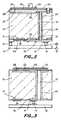
- FIG. 1is a perspective view of micromachined devices (MEMS) with through wafer interconnects;
- MEMSmicromachined devices
- FIG. 2is a sectional view showing a wafer with a through wafer interconnect in accordance with our embodiment of the present invention
- FIG. 3is a sectional view showing a wafer with a through wafer interconnect in accordance with still a further embodiment of the present invention
- FIG. 4is a sectional view showing a wafer with a through wafer interconnect in accordance with still another embodiment of the present invention.
- FIG. 5is a sectional view showing a wafer with a through wafer interconnect in accordance with still another embodiment of the present invention.
- FIG. 6is a curve showing the expected capacitance-voltage relationship for a pn junction interconnect
- FIG. 7shows the process steps for fabricating a wafer with through wafer MIS vias and pn-junction pads
- FIG. 8shows the process steps for fabricating a wafer with through wafer interconnect with pn junction vias and pads
- FIG. 9shows the process steps for fabricating a wafer with through wafer interconnect with MIS vias and pads
- FIG. 10schematically shows a wafer with through wafer interconnects with trenches for reduction of thermal mismatch between the device array and the electronics.
- FIG. 1shows MEMS devices 11 connected to integrated circuits 12 with through wafer interconnects 13 and solder bumps 14 .
- the integrated circuit (electronics) 12is shown wire bonded 16 to a printed circuit board 17 .
- the MEMS arrayis connected with the electronic circuits without sacrificing the performance of either one and minimizing the parasitic capacitance.
- the parasitic capacitance of the interconnect between an array element and its electronicsis the limiting factor for the dynamic range and frequency bandwidth. Therefore, it is always best to put the electronics as close to the array elements as possible.
- an electrical through wafer interconnectis employed to address the array elements individually, where the front side of the wafer is fully populated with the array elements and the backside is solely dedicated to bond pads for the flip-chip bonding to the printed circuit board (PCB) or the integrated circuits as shown in FIG. 1 .
- the parasitics due to any interconnection cable or tracesare avoided.
- the parasitic capacitance of the ETWI to the silicon substrateneeds to be reduced to a comparatively lower level than the device capacitance.
- One of the solutions for the parasitic reductionis to implement reverse-biased pn junction on the front and backside pads of the wafer and an MIS junction interconnects.
- the transducerincludes active cells 23 , which comprise flexible membranes 24 having a top (ground) electrode 26 supported by insulating supports 27 and a bottom signal electrode 28 .
- active cells 23which comprise flexible membranes 24 having a top (ground) electrode 26 supported by insulating supports 27 and a bottom signal electrode 28 .
- the top electrodeis connected to ground 29 through ohmic contact 31 with the wafer 21 .
- the bottom electrode 28comprises the top side pad and is connected to the back side pad 32 by via conductor 33 formed on the oxide layer 34 grown in the via 36 .
- the viamay be sealed by polysilicon filler 37 .
- Diffusion regions 38 and 39are formed in the wafer or substrate 21 and define pn junctions which can be reverse biased by applying a dc voltage to the interconnect and pads to provide a depletion layer. When the pn junctions are reverse biased, the high resistivity (>1000 ohm-cm) silicon substrate is fully depleted achieving a low parasitic capacitance at the top side and back side pads.
- the back side padsare connected to the processing or integrated circuit 12 by solder pads 41 and solder bumps 14 .
- FIG. 3Another solution for parasitic capacitance reduction is to implement reverse biased pn-junction diodes inside the interconnects as well as at the pads as shown in FIG. 3 .
- the front side pads 28 , back side pads 32 and the through via interconnects 44comprise highly doped regions which serve as the conductors. The regions form pn junctions which can be reverse biased.
- the expected capacitance-voltage relationshipis show in FIG. 6 .
- the predicted series resistanceis 434 which assumes that the doping profile is the same for the surfaces on top of the wafer and inside the via holes.
- MIS junctionis implemented inside the interconnects at the pads as well as inside the interconnects as shown in FIG. 4 .
- the MIS junctionwill give a better electrical isolation for high voltage applications. It will also give certain amount of parasitic capacitance reduction when biasing to depletion although not as good as using reverse-biased pn junction.
- FIG. 4parts like those in FIG. 2 have the same reference numbers and are not further described.
- the front side pads 28 , back side pads 32 and the through via interconnects 33comprise doped polysilicon which serve as the conductors.
- the regionsform MIS junction which can be biased to depletion.
- the high resistivity (>1000 ohm-cm) silicon substrateis depleted to certain width (>9 m)achieving a low parasitic capacitance at the via, the top side, and the back side pads.
- Another solution for the parasitic reductionis to implement reverse-biased Schottky diodes on the front and backside pads of the wafer and inside the interconnects as shown in FIG. 5 .
- the top side, back side pads 47 and 46 , interconnect 48are a metal which form Schottky junctions with the substrate.
- Like reference numbershave been applied to parts like in FIGS. 2 and 3.
- With a reverse bias dc voltage applied to the Schottky diodethe high resistivity (>1000 ohm-cm) silicon substrate is fully depleted of electrons. Thus a low capacitance is achieved.
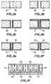
- FIG. 7The process flow for forming a wafer with through wafer interconnects of the type shown in FIG. 2 is shown in FIG. 7 .
- a 400 ⁇ m thick double-sided polished silicon wafer 51which is thermally oxidized to 2 ⁇ m thick to serve as a hard mask for the deep etch. Both sides are then patterned with 20 ⁇ m diameter openings for each interconnect.
- a through-wafer deep etchis done by etching halfway from both sides of the wafer (FIG. 7 a ). By this means, a 20 to 1 high aspect ration via hole 54 , can be achieved.
- the oxide maskis then removed by buffered oxide etch (BOE).
- BOEbuffered oxide etch
- interconnect side walls and wafer front and backside padsare grown with 1 ⁇ m of thermal oxide 56 (FIG. 7 b ).
- a layer 57 of 2 ⁇ m polysiliconis deposited and then heavily doped with boron or phosphorous depending on the wafer type to enhance the conductance (FIG. 7 c ).
- a layer 58 of low temperature oxide (LTO)is deposited to serve as an etching stop for the etch-back of polysilicon deposited in the following step.
- the interconnect holesare then filled with polysilicon 59 (FIG. 7 d ).
- the polysilicon on both sidesis then etched back and stopped on the LTO (FIG. 7 e ).
- the 2 ⁇ m doped polysiliconis exposed again and ready to be etched for the front and back side oxide opening 61 (FIG. 7 f ).
- Another layer 62 of 0.5 ⁇ m polysiliconis deposited and doped with boron or phosphorous (FIG. 7 g ).
- the front and back side polysilicon padsare patterned followed by the oxide etch on the back side for ground opening 63 and heavily doped for ohmic contact. After this step, the array of devices can be built on top of the front side polysilicon.
- FIG. 8The process flow for fabricating a wafer with through wafer interconnects of the type shown in FIG. 3 is shown in FIG. 8 .
- a 400 ⁇ m thick double-sided polished Si wafer 71which is thermally oxidized to 2 ⁇ m thick 72 to serve as a hard mask for the deep etch. Both sides are then patterned with 20 ⁇ m diameter openings 73 for each interconnect (FIG. 8 a ).
- the through-wafer deep etchis done by etching half way from both sides of the wafer (FIG. 8 b ). By this means, a 20 to 1 high aspect ratio via hole can be achieved.
- the waferis then heavily doped with boron or phosphorous 74 depending on the wafer type to build the pn junction diode inside the holes (FIG. 8 c ).
- the interconnect holesare then filled with polysilicon 76 (FIG. 8 d ).
- the polysilicon on both sidesis then etched back and stopped on the oxide (FIG. 8 e ). It is ready to be etched for the front and back side oxide opening 77 (FIG. 8 f ).
- the waferis then doped with boron 78 which makes up the pn junctions for the front and back side pads 81 , 82 .
- the oxideis etched on the back side for ground opening 63 and heavily doped for ohmic contact 83 . After this step, the array of devices can be built on top of the front side pn junction pad.
- FIG. 9The process flow for forming a wafer with through wafer interconnects of the type shown in FIG. 4 is shown in FIG. 9 .
- a 400 m thick double-sided polished silicon wafer 86which is thermally oxidized to 2 m thick to serve as a hard mask for the deep etch. Both sides are then patterned with 20 m diameter openings for each interconnect.
- a through-wafer deep etchis done by etching halfway from both sides of the wafer (FIG. 9 a ). By this means, a 20 to 1 high aspect ration via hole 87 , can be achieved.
- the oxide maskis then removed by buffered oxide etch (BOE).
- interconnect side walls and wafer front and backside padsare grown with 1 m of thermal oxide 88 (FIG. 9 b ).
- a layer 89 of 2 m polysiliconis deposited and then heavily doped with boron or phosphorous to enhance the conductance (FIG. 9 c ).
- a layer 91 of low temperature oxide (LTO)is deposited to serve as an etching stop for the etch-back of polysilicon deposited in the following step.
- the interconnect holesare then filled with polysilicon 92 (FIG. 9 d ).
- the polysilicon on both sidesis then etched back and stopped on the LTO (FIG. 9 e ).
- the 2 m doped polysiliconis exposed again and ready to be etched for the front and back side pads 93 , 94 patterning (FIG. 9 f ).
- the oxideis opened on the back side for ground opening 96 and heavily doped for ohmic contact. After this step, the array of devices can be built on top of the front side polysilicon.
- a wafer 101 with through via interconnects 102 and top side and bottom side pads 103 and 104is schematically shown.
- This waferis flip chip bonded to a integrated or processing circuit 106 or to a printed circuit board by solder bumps 107 .
- Trenches 108are etched in the wafer to reduce lateral stiffness at the surface of the wafer. Stress induced by thermal expansion differences between the wafer and associated connected devices is reduced, extending the lifetime of the assembly by reducing fatigue due to the thermal expansion differences.
- a wafer with high density and low parasitic capacitance electrical through-wafer interconnects (vias) for connection to an array of micromachined transducers or devices on a silicon waferhas been described.
- the waferprovides vertical wafer feedthroughs (interconnects) connecting an array of sensors or actuators from the front side (transducer side) to the backside (packaging side) of the wafer.
- a 20 to 1 high aspect ratio 400 ⁇ m long and 20 ⁇ m diameter interconnectis achieved by using deep reactive ion etching (DRIE).
- DRIEdeep reactive ion etching
- Reduction of the parasitic capacitance to the substrateis achieved using reverse-biased pn junction diodes.
- a parasitic capacitance of 0.05 pFhas been demonstrated by this approach.
- This three-dimensional architectureallows for elegant wafer-level packaging through simple flip-chip bonding of the chip's backside to a printed circuit board (PCB) or a signal processing circuit.
- PCBprinted circuit board
Landscapes
- Engineering & Computer Science (AREA)
- Mechanical Engineering (AREA)
- Physics & Mathematics (AREA)
- Condensed Matter Physics & Semiconductors (AREA)
- General Physics & Mathematics (AREA)
- Manufacturing & Machinery (AREA)
- Computer Hardware Design (AREA)
- Microelectronics & Electronic Packaging (AREA)
- Power Engineering (AREA)
- Internal Circuitry In Semiconductor Integrated Circuit Devices (AREA)
- Semiconductor Integrated Circuits (AREA)
Abstract
Description
Claims (20)
Priority Applications (1)
| Application Number | Priority Date | Filing Date | Title |
|---|---|---|---|
| US10/349,597US6836020B2 (en) | 2003-01-22 | 2003-01-22 | Electrical through wafer interconnects |
Applications Claiming Priority (1)
| Application Number | Priority Date | Filing Date | Title |
|---|---|---|---|
| US10/349,597US6836020B2 (en) | 2003-01-22 | 2003-01-22 | Electrical through wafer interconnects |
Publications (2)
| Publication Number | Publication Date |
|---|---|
| US20040141421A1 US20040141421A1 (en) | 2004-07-22 |
| US6836020B2true US6836020B2 (en) | 2004-12-28 |
Family
ID=32712759
Family Applications (1)
| Application Number | Title | Priority Date | Filing Date |
|---|---|---|---|
| US10/349,597Expired - LifetimeUS6836020B2 (en) | 2003-01-22 | 2003-01-22 | Electrical through wafer interconnects |
Country Status (1)
| Country | Link |
|---|---|
| US (1) | US6836020B2 (en) |
Cited By (34)
| Publication number | Priority date | Publication date | Assignee | Title |
|---|---|---|---|---|
| US20040188826A1 (en)* | 2003-03-31 | 2004-09-30 | Palanduz Cengiz A. | Interposer with signal and power supply through vias |
| US20060097290A1 (en)* | 2002-07-26 | 2006-05-11 | Iiro Hietanen | Semiconductor structure for imaging detectors |
| US20060289777A1 (en)* | 2005-06-29 | 2006-12-28 | Wen Li | Detector with electrically isolated pixels |
| US20070085215A1 (en)* | 2003-09-30 | 2007-04-19 | Budd Russell A | Silicon based optical vias |
| US20070278699A1 (en)* | 2006-05-31 | 2007-12-06 | Lucent Technologies Inc. | Microelectronic element chips |
| US7321181B2 (en) | 2004-04-07 | 2008-01-22 | The Board Of Trustees Of The Leland Stanford Junior University | Capacitive membrane ultrasonic transducers with reduced bulk wave generation and method |
| US20080048211A1 (en)* | 2006-07-20 | 2008-02-28 | Khuri-Yakub Butrus T | Trench isolated capacitive micromachined ultrasonic transducer arrays with a supporting frame |
| EP1918027A1 (en) | 2006-10-30 | 2008-05-07 | Olympus Medical Systems Corp. | Ultrasonic transducer, method for manufacturing ultrasonic transducer, and ultrasonic endoscope |
| US20090122651A1 (en)* | 2007-10-18 | 2009-05-14 | Mario Kupnik | Direct wafer bonded 2-D CUMT array |
| US20090130806A1 (en)* | 2005-10-25 | 2009-05-21 | Infineon Technologies Austria Ag | Power semiconductor component with charge compensation structure and method for the fabrication thereof |
| US20090218698A1 (en)* | 2008-02-28 | 2009-09-03 | Atmel Corporation | Wafer-Level Integrated Circuit Package with Top and Bottom Side Electrical Connections |
| US20100020511A1 (en)* | 2008-07-25 | 2010-01-28 | Honeywell International, Inc. | Stiffening support for printed circuit assemblies |
| US20100032811A1 (en)* | 2008-08-08 | 2010-02-11 | Hanyi Ding | Through wafer vias and method of making same |
| WO2010017031A1 (en)* | 2008-08-08 | 2010-02-11 | International Business Machines Corporation | Through wafer via and method of making same |
| US20100032810A1 (en)* | 2008-08-08 | 2010-02-11 | Hanyi Ding | Through wafer vias and method of making same |
| US20100032764A1 (en)* | 2008-08-08 | 2010-02-11 | Paul Stephen Andry | Through silicon via and method of fabricating same |
| US20100225200A1 (en)* | 2009-03-05 | 2010-09-09 | Mario Kupnik | Monolithic integrated CMUTs fabricated by low-temperature wafer bonding |
| US7851925B2 (en) | 2008-09-19 | 2010-12-14 | Infineon Technologies Ag | Wafer level packaged MEMS integrated circuit |
| US20110057321A1 (en)* | 2009-09-08 | 2011-03-10 | Industrial Technology Research Institute | 3-d multi-wafer stacked semiconductor structure and method for manufacturing the same |
| US20120091543A1 (en)* | 2010-10-15 | 2012-04-19 | Canon Kabushiki Kaisha | Electromechanical transducer and method of manufacturing the same |
| US8343781B2 (en) | 2010-09-21 | 2013-01-01 | International Business Machines Corporation | Electrical mask inspection |
| US20130155817A1 (en)* | 2011-12-19 | 2013-06-20 | Samsung Electronics Co., Ltd. | Cell, element of ultrasonic transducer, ultrasonic transducer including the same, and method of manufacturing cell of ultrasonic transducer |
| US20130241021A1 (en)* | 2012-03-16 | 2013-09-19 | Analog Devices, Inc. | Integrated circuit having a semiconducting via; an integrated circuit including a sensor, such as a photosensitive device, and a method of making said integrated circuit |
| US8724832B2 (en) | 2011-08-30 | 2014-05-13 | Qualcomm Mems Technologies, Inc. | Piezoelectric microphone fabricated on glass |
| US8811636B2 (en) | 2011-11-29 | 2014-08-19 | Qualcomm Mems Technologies, Inc. | Microspeaker with piezoelectric, metal and dielectric membrane |
| US8824706B2 (en) | 2011-08-30 | 2014-09-02 | Qualcomm Mems Technologies, Inc. | Piezoelectric microphone fabricated on glass |
| US8852103B2 (en) | 2011-10-17 | 2014-10-07 | Butterfly Network, Inc. | Transmissive imaging and related apparatus and methods |
| JP2015128271A (en)* | 2013-12-28 | 2015-07-09 | キヤノン株式会社 | Capacitive transducer and manufacturing method thereof |
| US9142665B2 (en) | 2010-12-10 | 2015-09-22 | Infineon Technologies Austria Ag | Semiconductor component with a semiconductor via |
| US9396997B2 (en) | 2010-12-10 | 2016-07-19 | Infineon Technologies Ag | Method for producing a semiconductor component with insulated semiconductor mesas |
| US9667889B2 (en) | 2013-04-03 | 2017-05-30 | Butterfly Network, Inc. | Portable electronic devices with integrated imaging capabilities |
| US20230268318A1 (en)* | 2022-02-18 | 2023-08-24 | Micron Technology, Inc. | Methods and assemblies for measurement and prediction of package and die strength |
| US12172188B2 (en) | 2021-03-04 | 2024-12-24 | Bfly Operations, Inc. | Micromachined ultrasound transducer with pedestal |
| US12246348B2 (en) | 2021-03-04 | 2025-03-11 | BFLY Operations, Inc | Capacitive Micromachined ultrasonic transducers (CMUTs) having non-uniform pedestals |
Families Citing this family (11)
| Publication number | Priority date | Publication date | Assignee | Title |
|---|---|---|---|---|
| US7361581B2 (en)* | 2004-11-23 | 2008-04-22 | International Business Machines Corporation | High surface area aluminum bond pad for through-wafer connections to an electronic package |
| US7276794B2 (en)* | 2005-03-02 | 2007-10-02 | Endevco Corporation | Junction-isolated vias |
| US20080296708A1 (en)* | 2007-05-31 | 2008-12-04 | General Electric Company | Integrated sensor arrays and method for making and using such arrays |
| US7781238B2 (en)* | 2007-12-06 | 2010-08-24 | Robert Gideon Wodnicki | Methods of making and using integrated and testable sensor array |
| WO2013057642A1 (en)* | 2011-10-17 | 2013-04-25 | Koninklijke Philips Electronics N.V. | Through-wafer via device and method of manufacturing the same |
| TWI607534B (en)* | 2013-04-19 | 2017-12-01 | 精材科技股份有限公司 | Chip package and manufacturing method thereof |
| US10864551B2 (en) | 2014-12-15 | 2020-12-15 | Koninklijke Philips, N.V. | Compact ultrasound transducer with direct coax attachment |
| AU2019350989A1 (en) | 2018-09-28 | 2021-03-25 | Butterfly Network, Inc. | Fabrication techniques and structures for gettering materials in ultrasonic transducer cavities |
| WO2020210470A1 (en)* | 2019-04-12 | 2020-10-15 | Butterfly Network, Inc. | Bottom electrode via structures for micromachined ultrasonic transducer devices |
| KR102842579B1 (en) | 2020-04-01 | 2025-08-06 | 에스케이하이닉스 주식회사 | Image sensor device |
| KR20210122526A (en) | 2020-04-01 | 2021-10-12 | 에스케이하이닉스 주식회사 | Image sensor device |
Citations (4)
| Publication number | Priority date | Publication date | Assignee | Title |
|---|---|---|---|---|
| US5619476A (en)* | 1994-10-21 | 1997-04-08 | The Board Of Trustees Of The Leland Stanford Jr. Univ. | Electrostatic ultrasonic transducer |
| US5894452A (en)* | 1994-10-21 | 1999-04-13 | The Board Of Trustees Of The Leland Stanford Junior University | Microfabricated ultrasonic immersion transducer |
| US6430109B1 (en)* | 1999-09-30 | 2002-08-06 | The Board Of Trustees Of The Leland Stanford Junior University | Array of capacitive micromachined ultrasonic transducer elements with through wafer via connections |
| US6674126B2 (en)* | 2001-02-09 | 2004-01-06 | Fuji Electric Co., Ltd. | Semiconductor device |
- 2003
- 2003-01-22USUS10/349,597patent/US6836020B2/ennot_activeExpired - Lifetime
Patent Citations (5)
| Publication number | Priority date | Publication date | Assignee | Title |
|---|---|---|---|---|
| US5619476A (en)* | 1994-10-21 | 1997-04-08 | The Board Of Trustees Of The Leland Stanford Jr. Univ. | Electrostatic ultrasonic transducer |
| US5870351A (en)* | 1994-10-21 | 1999-02-09 | The Board Of Trustees Of The Leland Stanford Junior University | Broadband microfabriated ultrasonic transducer and method of fabrication |
| US5894452A (en)* | 1994-10-21 | 1999-04-13 | The Board Of Trustees Of The Leland Stanford Junior University | Microfabricated ultrasonic immersion transducer |
| US6430109B1 (en)* | 1999-09-30 | 2002-08-06 | The Board Of Trustees Of The Leland Stanford Junior University | Array of capacitive micromachined ultrasonic transducer elements with through wafer via connections |
| US6674126B2 (en)* | 2001-02-09 | 2004-01-06 | Fuji Electric Co., Ltd. | Semiconductor device |
Non-Patent Citations (21)
| Title |
|---|
| Alizadeh-Taheri, B., et al., "An Active, Microfabricated, Scalp Electrode-Array for EEG Recording", Transducers '95-Eurosensers IX, The 8<th >International Conference on Solid-State Sensors and Actuators, and Eurosensors IX, Stockholm, Sweden, Jun. 25-29, 1995, pp. 67-70. |
| Alizadeh-Taheri, B., et al., "An Active, Microfabricated, Scalp Electrode-Array for EEG Recording", Transducers '95—Eurosensers IX, The 8th International Conference on Solid-State Sensors and Actuators, and Eurosensors IX, Stockholm, Sweden, Jun. 25-29, 1995, pp. 67-70. |
| Bollmann, D., et al., "Invited paper: Three Dimensional Metallization for Vertically Integrated Circuits", Materials for Advanced Metallization, 1997, pp. 94-98. |
| Burger, G.J., et al., "High Resolution Shadow Mask Patterning in Deep Holes and Its Application to an Electrical Wafer Feed-Through", Transducers '95-Eurosensors IX, The 8<th >International Conference on Solid-State Sensors and Actuators, and Eurosensors IX. Stockholm, Sweden, Jun. 25-29, 1995, pp. 573-576. |
| Burger, G.J., et al., "High Resolution Shadow Mask Patterning in Deep Holes and Its Application to an Electrical Wafer Feed-Through", Transducers '95—Eurosensors IX, The 8th International Conference on Solid-State Sensors and Actuators, and Eurosensors IX. Stockholm, Sweden, Jun. 25-29, 1995, pp. 573-576. |
| Calmes, S., et al., "Highly Integrated 2-D Capacitive Micromachined Ultrasonic Transducers", 1999 IEEE Ultrasonics Symposium, IEEE, 1999, pp. 1163-1166. |
| Cheng, C.H., et al., "An Efficient Electrical Addressing Method Using Through-Wafer Vias for Two-Dimensional Ultrasonic Arrays", 2000 IEEE Ultrasonics Symposium, IEEE , 2000, pp. 1179-1182. |
| Christensen, C., et al., "Wafer Through-Hole Interconnections with High Vertical Wiring Densities", IEEE, Dec. 1996, 19(4):516-522. |
| Fujita, Y., et al., "Feasibility Study on Through-Wafer Interconnecting Method for Hybrid Wafer-Scale -Integration", IEEE, 1999, pp. 1081-1084. |
| Heschel, M., et al., "Conformal Coating By Photoresist Of Sharp Corners Of Anisotropically Etched Through-Holes In Silicon", Transducers '97, 1997 International Conference on Solid-State and Actuators, Chicago, Jun. 16-19, 1997, pp. 209-212. |
| Kallis, J.M., et al., "Reliability of the 3-D Computer Under Stress of Mechanical Vibration and Thermal Cycling", IEEE, 1989, pp. 65-72. |
| Kuhmann, J.F., et al., "Through Wafer Interconnects and Flip-Chip Bonding: A Toolbox for Advanced Hybrid Technologies for MEMS", Eurosensors XIII, The 13<th >European Conference on Solid-State Transducers, Sep. 12-15, 1999, The Hague, The Netherlands, pp. 265-272. |
| Kuhmann, J.F., et al., "Through Wafer Interconnects and Flip-Chip Bonding: A Toolbox for Advanced Hybrid Technologies for MEMS", Eurosensors XIII, The 13th European Conference on Solid-State Transducers, Sep. 12-15, 1999, The Hague, The Netherlands, pp. 265-272. |
| Li, X., et al., "High Density Electrical Feedthrough Fabricated by Deep Reactive Ion Etching of Pyrex Glass", IEEE, 2001, pp. 98-101. |
| Linder, S., et al., "Fabrication Technology for Wafer Through-Hole Interconnections and Three-Dimensional Stacks of Chips and Wafers", IEEE, 1994, pp. 349-354. |
| Little, M.J., et al., "The 3-D Computer", IEEE, 1989, pp. 55-72. |
| Liu, C., et al., "Through-Wafer Electrical Interconnects by Sidewall Photolithographic Patterning", IEEE, 1998, pp. 1402-1405. |
| Mita, Y., et al., "Two Dimensional Micro Conveyance System with Through Holes for Electrical and Fluidic Interconnection", Transducers '97, 1997 International Conference on Solid-State Sensors and Actuators, Chicago, Jun. 16-19, 1997, IEEE, 1997, pp. 37-40. |
| Nguyen, N.T., et al., "Through-wafer copper electroplating for three-dimensional interconnects", J. Micromech. Microeng., 2002, 12:395-399. |
| Takahata, K., et al., "Batch Mode Micro-EDM for High-Density and High-Throughput Micromachining", IEEE, 2001, pp. 72-75. |
| Wu, J.H., et al., "A High Aspect-Ratio Silicon Substrate-Via Technology and Applications: Through-Wafer Interconnects for Power and Ground and Faraday Cages for SOC Isolation", IEEE, 2000, pp. 477-480. |
Cited By (78)
| Publication number | Priority date | Publication date | Assignee | Title |
|---|---|---|---|---|
| US8159049B2 (en) | 2002-07-26 | 2012-04-17 | Detection Technology Oy | Semiconductor structure for imaging detectors |
| US20060097290A1 (en)* | 2002-07-26 | 2006-05-11 | Iiro Hietanen | Semiconductor structure for imaging detectors |
| US7081650B2 (en)* | 2003-03-31 | 2006-07-25 | Intel Corporation | Interposer with signal and power supply through vias |
| US20040188826A1 (en)* | 2003-03-31 | 2004-09-30 | Palanduz Cengiz A. | Interposer with signal and power supply through vias |
| US7352066B2 (en)* | 2003-09-30 | 2008-04-01 | International Business Machines Corporation | Silicon based optical vias |
| US20070085215A1 (en)* | 2003-09-30 | 2007-04-19 | Budd Russell A | Silicon based optical vias |
| US7321181B2 (en) | 2004-04-07 | 2008-01-22 | The Board Of Trustees Of The Leland Stanford Junior University | Capacitive membrane ultrasonic transducers with reduced bulk wave generation and method |
| US20060289777A1 (en)* | 2005-06-29 | 2006-12-28 | Wen Li | Detector with electrically isolated pixels |
| US8263450B2 (en)* | 2005-10-25 | 2012-09-11 | Infineon Technologies Ag | Power semiconductor component with charge compensation structure and method for the fabrication thereof |
| US20090130806A1 (en)* | 2005-10-25 | 2009-05-21 | Infineon Technologies Austria Ag | Power semiconductor component with charge compensation structure and method for the fabrication thereof |
| US20070278699A1 (en)* | 2006-05-31 | 2007-12-06 | Lucent Technologies Inc. | Microelectronic element chips |
| US8343807B2 (en) | 2006-05-31 | 2013-01-01 | Alcatel Lucent | Process for making microelectronic element chips |
| US7474005B2 (en)* | 2006-05-31 | 2009-01-06 | Alcatel-Lucent Usa Inc. | Microelectronic element chips |
| US20090075424A1 (en)* | 2006-05-31 | 2009-03-19 | Alcatel-Lucent Usa Inc. | Process for making microelectronic element chips |
| US20080048211A1 (en)* | 2006-07-20 | 2008-02-28 | Khuri-Yakub Butrus T | Trench isolated capacitive micromachined ultrasonic transducer arrays with a supporting frame |
| US7741686B2 (en)* | 2006-07-20 | 2010-06-22 | The Board Of Trustees Of The Leland Stanford Junior University | Trench isolated capacitive micromachined ultrasonic transducer arrays with a supporting frame |
| US8740800B2 (en) | 2006-10-30 | 2014-06-03 | Olympus Medical Systems Corp. | Ultrasonic transducer, method for manufacturing ultrasonic transducer, and ultrasonic endoscope |
| EP1918027A1 (en) | 2006-10-30 | 2008-05-07 | Olympus Medical Systems Corp. | Ultrasonic transducer, method for manufacturing ultrasonic transducer, and ultrasonic endoscope |
| US20080200811A1 (en)* | 2006-10-30 | 2008-08-21 | Olympus Medical Systems Corp. | Ultrasonic transducer, method for manufacturing ultrasonic transducer, and ultrasonic endoscope |
| US7846102B2 (en)* | 2007-10-18 | 2010-12-07 | The Board Of Trustees Of The Leland Stanford Junior University | Direct wafer bonded 2-D CUMT array |
| US20090122651A1 (en)* | 2007-10-18 | 2009-05-14 | Mario Kupnik | Direct wafer bonded 2-D CUMT array |
| US8018065B2 (en) | 2008-02-28 | 2011-09-13 | Atmel Corporation | Wafer-level integrated circuit package with top and bottom side electrical connections |
| US20090218698A1 (en)* | 2008-02-28 | 2009-09-03 | Atmel Corporation | Wafer-Level Integrated Circuit Package with Top and Bottom Side Electrical Connections |
| US20100020511A1 (en)* | 2008-07-25 | 2010-01-28 | Honeywell International, Inc. | Stiffening support for printed circuit assemblies |
| US7869220B2 (en) | 2008-07-25 | 2011-01-11 | Honeywell International Inc. | Stiffening support for printed circuit assemblies |
| US8138036B2 (en) | 2008-08-08 | 2012-03-20 | International Business Machines Corporation | Through silicon via and method of fabricating same |
| US8735251B2 (en) | 2008-08-08 | 2014-05-27 | Ultratech, Inc. | Through silicon via and method of fabricating same |
| US20100032811A1 (en)* | 2008-08-08 | 2010-02-11 | Hanyi Ding | Through wafer vias and method of making same |
| US20100032764A1 (en)* | 2008-08-08 | 2010-02-11 | Paul Stephen Andry | Through silicon via and method of fabricating same |
| US8035198B2 (en) | 2008-08-08 | 2011-10-11 | International Business Machines Corporation | Through wafer via and method of making same |
| US8748308B2 (en) | 2008-08-08 | 2014-06-10 | International Business Machines Corporation | Through wafer vias and method of making same |
| US20100032808A1 (en)* | 2008-08-08 | 2010-02-11 | Hanyi Ding | Through wafer via and method of making same |
| US8384224B2 (en) | 2008-08-08 | 2013-02-26 | International Business Machines Corporation | Through wafer vias and method of making same |
| US8637937B2 (en) | 2008-08-08 | 2014-01-28 | Ultratech, Inc. | Through silicon via for use in integrated circuit chips |
| US20100032810A1 (en)* | 2008-08-08 | 2010-02-11 | Hanyi Ding | Through wafer vias and method of making same |
| US8299566B2 (en) | 2008-08-08 | 2012-10-30 | International Business Machines Corporation | Through wafer vias and method of making same |
| WO2010017031A1 (en)* | 2008-08-08 | 2010-02-11 | International Business Machines Corporation | Through wafer via and method of making same |
| US8518787B2 (en) | 2008-08-08 | 2013-08-27 | International Business Machines Corporation | Through wafer vias and method of making same |
| US7851925B2 (en) | 2008-09-19 | 2010-12-14 | Infineon Technologies Ag | Wafer level packaged MEMS integrated circuit |
| US8402831B2 (en)* | 2009-03-05 | 2013-03-26 | The Board Of Trustees Of The Leland Standford Junior University | Monolithic integrated CMUTs fabricated by low-temperature wafer bonding |
| US20100225200A1 (en)* | 2009-03-05 | 2010-09-09 | Mario Kupnik | Monolithic integrated CMUTs fabricated by low-temperature wafer bonding |
| US20110057321A1 (en)* | 2009-09-08 | 2011-03-10 | Industrial Technology Research Institute | 3-d multi-wafer stacked semiconductor structure and method for manufacturing the same |
| US8343781B2 (en) | 2010-09-21 | 2013-01-01 | International Business Machines Corporation | Electrical mask inspection |
| CN102569306A (en)* | 2010-10-15 | 2012-07-11 | 佳能株式会社 | Electromechanical transducer and method of manufacturing the same |
| US8653613B2 (en)* | 2010-10-15 | 2014-02-18 | Canon Kabushiki Kaisha | Electromechanical transducer and method of manufacturing the same |
| US20140120646A1 (en)* | 2010-10-15 | 2014-05-01 | Canon Kabushiki Kaisha | Electromechanical transducer and method of manufacturing the same |
| US20120091543A1 (en)* | 2010-10-15 | 2012-04-19 | Canon Kabushiki Kaisha | Electromechanical transducer and method of manufacturing the same |
| US8980670B2 (en)* | 2010-10-15 | 2015-03-17 | Canon Kabushiki Kaisha | Electromechanical transducer and method of manufacturing the same |
| CN102569306B (en)* | 2010-10-15 | 2015-06-03 | 佳能株式会社 | Electromechanical transducer and method of manufacturing the same |
| US9634101B2 (en) | 2010-12-10 | 2017-04-25 | Infineon Technologies Austria Ag | Semiconductor component with a monocrystalline semiconductor region arranged in a via region |
| DE102011056157B4 (en) | 2010-12-10 | 2020-07-09 | Infineon Technologies Ag | Method for producing a semiconductor device and semiconductor devices with isolated semiconductor mesas |
| US9396997B2 (en) | 2010-12-10 | 2016-07-19 | Infineon Technologies Ag | Method for producing a semiconductor component with insulated semiconductor mesas |
| US9142665B2 (en) | 2010-12-10 | 2015-09-22 | Infineon Technologies Austria Ag | Semiconductor component with a semiconductor via |
| US8724832B2 (en) | 2011-08-30 | 2014-05-13 | Qualcomm Mems Technologies, Inc. | Piezoelectric microphone fabricated on glass |
| US8824706B2 (en) | 2011-08-30 | 2014-09-02 | Qualcomm Mems Technologies, Inc. | Piezoelectric microphone fabricated on glass |
| US9033884B2 (en) | 2011-10-17 | 2015-05-19 | Butterfly Network, Inc. | Transmissive imaging and related apparatus and methods |
| US9268015B2 (en) | 2011-10-17 | 2016-02-23 | Butterfly Network, Inc. | Image-guided high intensity focused ultrasound and related apparatus and methods |
| US9028412B2 (en) | 2011-10-17 | 2015-05-12 | Butterfly Network, Inc. | Transmissive imaging and related apparatus and methods |
| US9268014B2 (en) | 2011-10-17 | 2016-02-23 | Butterfly Network, Inc. | Transmissive imaging and related apparatus and methods |
| US9022936B2 (en) | 2011-10-17 | 2015-05-05 | Butterfly Network, Inc. | Transmissive imaging and related apparatus and methods |
| US9247924B2 (en) | 2011-10-17 | 2016-02-02 | Butterfly Networks, Inc. | Transmissive imaging and related apparatus and methods |
| US8852103B2 (en) | 2011-10-17 | 2014-10-07 | Butterfly Network, Inc. | Transmissive imaging and related apparatus and methods |
| US9149255B2 (en) | 2011-10-17 | 2015-10-06 | Butterfly Network, Inc. | Image-guided high intensity focused ultrasound and related apparatus and methods |
| US9155521B2 (en) | 2011-10-17 | 2015-10-13 | Butterfly Network, Inc. | Transmissive imaging and related apparatus and methods |
| US9198637B2 (en) | 2011-10-17 | 2015-12-01 | Butterfly Network, Inc. | Transmissive imaging and related apparatus and methods |
| US10003888B2 (en) | 2011-11-29 | 2018-06-19 | Snaptrack, Inc | Transducer with piezoelectric, conductive and dielectric membrane |
| US8811636B2 (en) | 2011-11-29 | 2014-08-19 | Qualcomm Mems Technologies, Inc. | Microspeaker with piezoelectric, metal and dielectric membrane |
| US10735865B2 (en) | 2011-11-29 | 2020-08-04 | Snaptrack, Inc. | Transducer with piezoelectric, conductive and dielectric membrane |
| US20130155817A1 (en)* | 2011-12-19 | 2013-06-20 | Samsung Electronics Co., Ltd. | Cell, element of ultrasonic transducer, ultrasonic transducer including the same, and method of manufacturing cell of ultrasonic transducer |
| US8687466B2 (en)* | 2011-12-19 | 2014-04-01 | Samsung Electronics Co., Ltd. | Cell, element of ultrasonic transducer, ultrasonic transducer including the same, and method of manufacturing cell of ultrasonic transducer |
| US8901697B2 (en)* | 2012-03-16 | 2014-12-02 | Analog Devices, Inc. | Integrated circuit having a semiconducting via; an integrated circuit including a sensor, such as a photosensitive device, and a method of making said integrated circuit |
| US20130241021A1 (en)* | 2012-03-16 | 2013-09-19 | Analog Devices, Inc. | Integrated circuit having a semiconducting via; an integrated circuit including a sensor, such as a photosensitive device, and a method of making said integrated circuit |
| US9667889B2 (en) | 2013-04-03 | 2017-05-30 | Butterfly Network, Inc. | Portable electronic devices with integrated imaging capabilities |
| JP2015128271A (en)* | 2013-12-28 | 2015-07-09 | キヤノン株式会社 | Capacitive transducer and manufacturing method thereof |
| US10018599B2 (en) | 2013-12-28 | 2018-07-10 | Canon Kabushiki Kaisha | Capacitive transducer and method of manufacturing the same |
| US12172188B2 (en) | 2021-03-04 | 2024-12-24 | Bfly Operations, Inc. | Micromachined ultrasound transducer with pedestal |
| US12246348B2 (en) | 2021-03-04 | 2025-03-11 | BFLY Operations, Inc | Capacitive Micromachined ultrasonic transducers (CMUTs) having non-uniform pedestals |
| US20230268318A1 (en)* | 2022-02-18 | 2023-08-24 | Micron Technology, Inc. | Methods and assemblies for measurement and prediction of package and die strength |
Also Published As
| Publication number | Publication date |
|---|---|
| US20040141421A1 (en) | 2004-07-22 |
Similar Documents
| Publication | Publication Date | Title |
|---|---|---|
| US6836020B2 (en) | Electrical through wafer interconnects | |
| US12272730B2 (en) | Transistor level interconnection methodologies utilizing 3D interconnects | |
| JP6306076B2 (en) | 3D device integration method and integrated device | |
| KR100882703B1 (en) | Semiconductor device and manufacturing method thereof, circuit board and manufacturing method thereof | |
| US6410859B1 (en) | Electrical assembly for semiconductor dice | |
| US7033927B2 (en) | Apparatus and method for thermal isolation, circuit cooling and electromagnetic shielding of a wafer | |
| KR101871866B1 (en) | Stacked microelectronic assembly having interposer connecting active chips | |
| US8105941B2 (en) | Through-wafer interconnection | |
| US5753529A (en) | Surface mount and flip chip technology for total integrated circuit isolation | |
| US6175141B1 (en) | Opto-electronic sensor component | |
| US20060197181A1 (en) | Semiconductor device, stacked structure, and manufacturing method | |
| JP4979213B2 (en) | Circuit board, circuit board manufacturing method, and circuit device | |
| US20020094661A1 (en) | Three dimensional device intergration method and intergrated device | |
| US20090114927A1 (en) | Multi-chips with an optical interconnection unit | |
| KR20120048558A (en) | Optoelectronic component | |
| CN118073965B (en) | Heterogeneous integrated structure, preparation method thereof and semiconductor device | |
| Cheng et al. | Electrical through-wafer interconnects with sub-picofarad parasitic capacitance [MEMS packaging] | |
| Cheng et al. | Electrical through wafer interconnects with 0.05 pico farads parasitic capacitance on 400 μm thick silicon substrate | |
| TWI373838B (en) | Component with semiconductor junction and its production method | |
| JP2006339232A (en) | Circuit board and its manufacturing method, and semiconductor device and its manufacturing method | |
| JP5025922B2 (en) | Circuit board, method for manufacturing circuit board, and semiconductor device | |
| TWI895301B (en) | High efficient micro devices | |
| TW202135270A (en) | High efficient micro devices | |
| CN116072598A (en) | Semiconductor device and method for manufacturing the same | |
| WO2020207917A1 (en) | Optoelectronic device, photonic detector and method of producing an optoelectronic device |
Legal Events
| Date | Code | Title | Description |
|---|---|---|---|
| AS | Assignment | Owner name:NAVY, SECRETARY OF THE UNITED STATES OF AMERICA, V Free format text:CONFIRMATORY LICENSE;ASSIGNOR:STANFORD UNIVERSITY;REEL/FRAME:014170/0545 Effective date:20030410 | |
| AS | Assignment | Owner name:BOARD OF TRUSTEES OF THE LELAND STANFORD JUNIOR UN Free format text:ASSIGNMENT OF ASSIGNORS INTEREST;ASSIGNORS:CHENG, CHING HSIANG;ERGUN, ARIF S.;KHURI-YAKUB, BUTRUS T.;REEL/FRAME:013773/0099 Effective date:20030617 | |
| STCF | Information on status: patent grant | Free format text:PATENTED CASE | |
| AS | Assignment | Owner name:NAVY, UNITED STATES OF AMERICA AS REPRESENTED BY T Free format text:CONFIRMATORY LICENSE;ASSIGNOR:STANFORD UNIVERSITY;REEL/FRAME:016621/0850 Effective date:20050113 | |
| FEPP | Fee payment procedure | Free format text:PAT HOLDER NO LONGER CLAIMS SMALL ENTITY STATUS, ENTITY STATUS SET TO UNDISCOUNTED (ORIGINAL EVENT CODE: STOL); ENTITY STATUS OF PATENT OWNER: LARGE ENTITY | |
| FPAY | Fee payment | Year of fee payment:4 | |
| FPAY | Fee payment | Year of fee payment:8 | |
| FPAY | Fee payment | Year of fee payment:12 |