US6835995B2 - Low dielectric constant material for integrated circuit fabrication - Google Patents
Low dielectric constant material for integrated circuit fabricationDownload PDFInfo
- Publication number
- US6835995B2 US6835995B2US10/033,656US3365601AUS6835995B2US 6835995 B2US6835995 B2US 6835995B2US 3365601 AUS3365601 AUS 3365601AUS 6835995 B2US6835995 B2US 6835995B2
- Authority
- US
- United States
- Prior art keywords
- planar
- dielectric constant
- layer
- low
- dielectric material
- Prior art date
- Legal status (The legal status is an assumption and is not a legal conclusion. Google has not performed a legal analysis and makes no representation as to the accuracy of the status listed.)
- Expired - Lifetime
Links
Images


Classifications
- H—ELECTRICITY
- H01—ELECTRIC ELEMENTS
- H01L—SEMICONDUCTOR DEVICES NOT COVERED BY CLASS H10
- H01L21/00—Processes or apparatus adapted for the manufacture or treatment of semiconductor or solid state devices or of parts thereof
- H01L21/02—Manufacture or treatment of semiconductor devices or of parts thereof
- H01L21/02104—Forming layers
- H01L21/02107—Forming insulating materials on a substrate
- H01L21/02109—Forming insulating materials on a substrate characterised by the type of layer, e.g. type of material, porous/non-porous, pre-cursors, mixtures or laminates
- H01L21/02112—Forming insulating materials on a substrate characterised by the type of layer, e.g. type of material, porous/non-porous, pre-cursors, mixtures or laminates characterised by the material of the layer
- H01L21/02123—Forming insulating materials on a substrate characterised by the type of layer, e.g. type of material, porous/non-porous, pre-cursors, mixtures or laminates characterised by the material of the layer the material containing silicon
- H01L21/02126—Forming insulating materials on a substrate characterised by the type of layer, e.g. type of material, porous/non-porous, pre-cursors, mixtures or laminates characterised by the material of the layer the material containing silicon the material containing Si, O, and at least one of H, N, C, F, or other non-metal elements, e.g. SiOC, SiOC:H or SiONC
- C—CHEMISTRY; METALLURGY
- C23—COATING METALLIC MATERIAL; COATING MATERIAL WITH METALLIC MATERIAL; CHEMICAL SURFACE TREATMENT; DIFFUSION TREATMENT OF METALLIC MATERIAL; COATING BY VACUUM EVAPORATION, BY SPUTTERING, BY ION IMPLANTATION OR BY CHEMICAL VAPOUR DEPOSITION, IN GENERAL; INHIBITING CORROSION OF METALLIC MATERIAL OR INCRUSTATION IN GENERAL
- C23C—COATING METALLIC MATERIAL; COATING MATERIAL WITH METALLIC MATERIAL; SURFACE TREATMENT OF METALLIC MATERIAL BY DIFFUSION INTO THE SURFACE, BY CHEMICAL CONVERSION OR SUBSTITUTION; COATING BY VACUUM EVAPORATION, BY SPUTTERING, BY ION IMPLANTATION OR BY CHEMICAL VAPOUR DEPOSITION, IN GENERAL
- C23C16/00—Chemical coating by decomposition of gaseous compounds, without leaving reaction products of surface material in the coating, i.e. chemical vapour deposition [CVD] processes
- C23C16/22—Chemical coating by decomposition of gaseous compounds, without leaving reaction products of surface material in the coating, i.e. chemical vapour deposition [CVD] processes characterised by the deposition of inorganic material, other than metallic material
- C23C16/30—Deposition of compounds, mixtures or solid solutions, e.g. borides, carbides, nitrides
- C—CHEMISTRY; METALLURGY
- C23—COATING METALLIC MATERIAL; COATING MATERIAL WITH METALLIC MATERIAL; CHEMICAL SURFACE TREATMENT; DIFFUSION TREATMENT OF METALLIC MATERIAL; COATING BY VACUUM EVAPORATION, BY SPUTTERING, BY ION IMPLANTATION OR BY CHEMICAL VAPOUR DEPOSITION, IN GENERAL; INHIBITING CORROSION OF METALLIC MATERIAL OR INCRUSTATION IN GENERAL
- C23C—COATING METALLIC MATERIAL; COATING MATERIAL WITH METALLIC MATERIAL; SURFACE TREATMENT OF METALLIC MATERIAL BY DIFFUSION INTO THE SURFACE, BY CHEMICAL CONVERSION OR SUBSTITUTION; COATING BY VACUUM EVAPORATION, BY SPUTTERING, BY ION IMPLANTATION OR BY CHEMICAL VAPOUR DEPOSITION, IN GENERAL
- C23C16/00—Chemical coating by decomposition of gaseous compounds, without leaving reaction products of surface material in the coating, i.e. chemical vapour deposition [CVD] processes
- C23C16/56—After-treatment
- H—ELECTRICITY
- H01—ELECTRIC ELEMENTS
- H01L—SEMICONDUCTOR DEVICES NOT COVERED BY CLASS H10
- H01L21/00—Processes or apparatus adapted for the manufacture or treatment of semiconductor or solid state devices or of parts thereof
- H01L21/02—Manufacture or treatment of semiconductor devices or of parts thereof
- H01L21/02104—Forming layers
- H01L21/02107—Forming insulating materials on a substrate
- H01L21/02225—Forming insulating materials on a substrate characterised by the process for the formation of the insulating layer
- H01L21/0226—Forming insulating materials on a substrate characterised by the process for the formation of the insulating layer formation by a deposition process
- H01L21/02263—Forming insulating materials on a substrate characterised by the process for the formation of the insulating layer formation by a deposition process deposition from the gas or vapour phase
- H01L21/02271—Forming insulating materials on a substrate characterised by the process for the formation of the insulating layer formation by a deposition process deposition from the gas or vapour phase deposition by decomposition or reaction of gaseous or vapour phase compounds, i.e. chemical vapour deposition
- H—ELECTRICITY
- H01—ELECTRIC ELEMENTS
- H01L—SEMICONDUCTOR DEVICES NOT COVERED BY CLASS H10
- H01L21/00—Processes or apparatus adapted for the manufacture or treatment of semiconductor or solid state devices or of parts thereof
- H01L21/02—Manufacture or treatment of semiconductor devices or of parts thereof
- H01L21/02104—Forming layers
- H01L21/02107—Forming insulating materials on a substrate
- H01L21/02296—Forming insulating materials on a substrate characterised by the treatment performed before or after the formation of the layer
- H01L21/02318—Forming insulating materials on a substrate characterised by the treatment performed before or after the formation of the layer post-treatment
- H01L21/02337—Forming insulating materials on a substrate characterised by the treatment performed before or after the formation of the layer post-treatment treatment by exposure to a gas or vapour
- H01L21/0234—Forming insulating materials on a substrate characterised by the treatment performed before or after the formation of the layer post-treatment treatment by exposure to a gas or vapour treatment by exposure to a plasma
- H—ELECTRICITY
- H01—ELECTRIC ELEMENTS
- H01L—SEMICONDUCTOR DEVICES NOT COVERED BY CLASS H10
- H01L21/00—Processes or apparatus adapted for the manufacture or treatment of semiconductor or solid state devices or of parts thereof
- H01L21/02—Manufacture or treatment of semiconductor devices or of parts thereof
- H01L21/02104—Forming layers
- H01L21/02107—Forming insulating materials on a substrate
- H01L21/02296—Forming insulating materials on a substrate characterised by the treatment performed before or after the formation of the layer
- H01L21/02318—Forming insulating materials on a substrate characterised by the treatment performed before or after the formation of the layer post-treatment
- H01L21/02362—Forming insulating materials on a substrate characterised by the treatment performed before or after the formation of the layer post-treatment formation of intermediate layers, e.g. capping layers or diffusion barriers
- H—ELECTRICITY
- H01—ELECTRIC ELEMENTS
- H01L—SEMICONDUCTOR DEVICES NOT COVERED BY CLASS H10
- H01L21/00—Processes or apparatus adapted for the manufacture or treatment of semiconductor or solid state devices or of parts thereof
- H01L21/02—Manufacture or treatment of semiconductor devices or of parts thereof
- H01L21/02104—Forming layers
- H01L21/02107—Forming insulating materials on a substrate
- H01L21/02109—Forming insulating materials on a substrate characterised by the type of layer, e.g. type of material, porous/non-porous, pre-cursors, mixtures or laminates
- H01L21/02112—Forming insulating materials on a substrate characterised by the type of layer, e.g. type of material, porous/non-porous, pre-cursors, mixtures or laminates characterised by the material of the layer
- H01L21/02123—Forming insulating materials on a substrate characterised by the type of layer, e.g. type of material, porous/non-porous, pre-cursors, mixtures or laminates characterised by the material of the layer the material containing silicon
- H01L21/02164—Forming insulating materials on a substrate characterised by the type of layer, e.g. type of material, porous/non-porous, pre-cursors, mixtures or laminates characterised by the material of the layer the material containing silicon the material being a silicon oxide, e.g. SiO2
- H—ELECTRICITY
- H01—ELECTRIC ELEMENTS
- H01L—SEMICONDUCTOR DEVICES NOT COVERED BY CLASS H10
- H01L21/00—Processes or apparatus adapted for the manufacture or treatment of semiconductor or solid state devices or of parts thereof
- H01L21/02—Manufacture or treatment of semiconductor devices or of parts thereof
- H01L21/02104—Forming layers
- H01L21/02107—Forming insulating materials on a substrate
- H01L21/02109—Forming insulating materials on a substrate characterised by the type of layer, e.g. type of material, porous/non-porous, pre-cursors, mixtures or laminates
- H01L21/02205—Forming insulating materials on a substrate characterised by the type of layer, e.g. type of material, porous/non-porous, pre-cursors, mixtures or laminates the layer being characterised by the precursor material for deposition
- H01L21/02208—Forming insulating materials on a substrate characterised by the type of layer, e.g. type of material, porous/non-porous, pre-cursors, mixtures or laminates the layer being characterised by the precursor material for deposition the precursor containing a compound comprising Si
- H01L21/02211—Forming insulating materials on a substrate characterised by the type of layer, e.g. type of material, porous/non-porous, pre-cursors, mixtures or laminates the layer being characterised by the precursor material for deposition the precursor containing a compound comprising Si the compound being a silane, e.g. disilane, methylsilane or chlorosilane
- H—ELECTRICITY
- H01—ELECTRIC ELEMENTS
- H01L—SEMICONDUCTOR DEVICES NOT COVERED BY CLASS H10
- H01L21/00—Processes or apparatus adapted for the manufacture or treatment of semiconductor or solid state devices or of parts thereof
- H01L21/02—Manufacture or treatment of semiconductor devices or of parts thereof
- H01L21/02104—Forming layers
- H01L21/02107—Forming insulating materials on a substrate
- H01L21/02109—Forming insulating materials on a substrate characterised by the type of layer, e.g. type of material, porous/non-porous, pre-cursors, mixtures or laminates
- H01L21/02205—Forming insulating materials on a substrate characterised by the type of layer, e.g. type of material, porous/non-porous, pre-cursors, mixtures or laminates the layer being characterised by the precursor material for deposition
- H01L21/02208—Forming insulating materials on a substrate characterised by the type of layer, e.g. type of material, porous/non-porous, pre-cursors, mixtures or laminates the layer being characterised by the precursor material for deposition the precursor containing a compound comprising Si
- H01L21/02214—Forming insulating materials on a substrate characterised by the type of layer, e.g. type of material, porous/non-porous, pre-cursors, mixtures or laminates the layer being characterised by the precursor material for deposition the precursor containing a compound comprising Si the compound comprising silicon and oxygen
- H01L21/02216—Forming insulating materials on a substrate characterised by the type of layer, e.g. type of material, porous/non-porous, pre-cursors, mixtures or laminates the layer being characterised by the precursor material for deposition the precursor containing a compound comprising Si the compound comprising silicon and oxygen the compound being a molecule comprising at least one silicon-oxygen bond and the compound having hydrogen or an organic group attached to the silicon or oxygen, e.g. a siloxane
- H—ELECTRICITY
- H01—ELECTRIC ELEMENTS
- H01L—SEMICONDUCTOR DEVICES NOT COVERED BY CLASS H10
- H01L21/00—Processes or apparatus adapted for the manufacture or treatment of semiconductor or solid state devices or of parts thereof
- H01L21/02—Manufacture or treatment of semiconductor devices or of parts thereof
- H01L21/02104—Forming layers
- H01L21/02107—Forming insulating materials on a substrate
- H01L21/02225—Forming insulating materials on a substrate characterised by the process for the formation of the insulating layer
- H01L21/0226—Forming insulating materials on a substrate characterised by the process for the formation of the insulating layer formation by a deposition process
- H01L21/02263—Forming insulating materials on a substrate characterised by the process for the formation of the insulating layer formation by a deposition process deposition from the gas or vapour phase
- H01L21/02271—Forming insulating materials on a substrate characterised by the process for the formation of the insulating layer formation by a deposition process deposition from the gas or vapour phase deposition by decomposition or reaction of gaseous or vapour phase compounds, i.e. chemical vapour deposition
- H01L21/02274—Forming insulating materials on a substrate characterised by the process for the formation of the insulating layer formation by a deposition process deposition from the gas or vapour phase deposition by decomposition or reaction of gaseous or vapour phase compounds, i.e. chemical vapour deposition in the presence of a plasma [PECVD]
- H—ELECTRICITY
- H01—ELECTRIC ELEMENTS
- H01L—SEMICONDUCTOR DEVICES NOT COVERED BY CLASS H10
- H01L21/00—Processes or apparatus adapted for the manufacture or treatment of semiconductor or solid state devices or of parts thereof
- H01L21/02—Manufacture or treatment of semiconductor devices or of parts thereof
- H01L21/02104—Forming layers
- H01L21/02107—Forming insulating materials on a substrate
- H01L21/02225—Forming insulating materials on a substrate characterised by the process for the formation of the insulating layer
- H01L21/0226—Forming insulating materials on a substrate characterised by the process for the formation of the insulating layer formation by a deposition process
- H01L21/02282—Forming insulating materials on a substrate characterised by the process for the formation of the insulating layer formation by a deposition process liquid deposition, e.g. spin-coating, sol-gel techniques, spray coating
- H—ELECTRICITY
- H01—ELECTRIC ELEMENTS
- H01L—SEMICONDUCTOR DEVICES NOT COVERED BY CLASS H10
- H01L21/00—Processes or apparatus adapted for the manufacture or treatment of semiconductor or solid state devices or of parts thereof
- H01L21/70—Manufacture or treatment of devices consisting of a plurality of solid state components formed in or on a common substrate or of parts thereof; Manufacture of integrated circuit devices or of parts thereof
- H01L21/71—Manufacture of specific parts of devices defined in group H01L21/70
- H01L21/768—Applying interconnections to be used for carrying current between separate components within a device comprising conductors and dielectrics
- H01L21/76801—Applying interconnections to be used for carrying current between separate components within a device comprising conductors and dielectrics characterised by the formation and the after-treatment of the dielectrics, e.g. smoothing
Definitions
- the present inventionrelates in general to materials for use with integrated circuits and methods of making the same, and in particular to insulating materials having low dielectric constants for electrical isolation in high density integrated circuits.
- ICsintegrated circuits
- layers of insulating, conducting and semiconducting materialsare deposited and patterned in sequence.
- the lowest levels or layers in the ICform electrical devices, such as transistors, separated by field isolation elements, with gate electrodes protected by insulating spacers.
- Memory cell capacitorsare also associated with the lower layers for certain circuits. These electrical devices are generally interconnected by patterned wiring layers and interlevel contacts formed above the devices.
- Conductive elementslike the transistor active areas and gates, capacitors, contacts and wiring layers, must each be electrically isolated from one another for proper circuit operation.
- the field isolation elementse.g., field oxide
- gate spacerscontribute to the isolation of transistor elements.
- Higher wiring layersinclude insulating material between the wiring layers, as well as between metal lines or runners within a wiring layer. Such insulating layers are often referred to as interlevel dielectrics (ILDs).
- IC operating speedcan be enhanced by reducing the parasitic capacitance between the metal lines.
- one way to reduce capacitanceis to use a material with a low dielectric constant (k).
- kdielectric constant
- Known processes to manufacture low k materialare unsatisfactory as they insufficiently lower the dielectric constant (relative to conventional oxides, for example) or cause difficulty when integrated with other necessary or desirable fabrication processes.
- the present inventionsatisfies these needs by providing materials having low dielectric constants for electrically isolating insulating material in ICs, and methods of manufacturing the same.
- the materialcan be formed with a low dielectric constant without the need for a cap layer.
- a method for providing electrical isolation between conductive elements in an integrated circuitincludes the provision of a substrate with a partially fabricated integrated circuit.
- An organosilane gas sourceis reacted with an oxidizing agent to form a layer over the substrate.
- the layeris predominantly formed of silicon hydroxide and incorporates carbon.
- This layeris then plasma treated without forming a layer during the plasma treatment. The treatment converts the silicon hydroxide layer to an insulating material having a lower dielectric constant.
- a processfor forming a low dielectric constant material.
- An organosilane gasis reacted to form a first material on a substrate.
- the first materialis then exposed to a plasma which contains oxygen in order to convert the first material to a second material without forming a layer over the first material.
- the second materialhas a dielectric constant of less than about 3.5.
- a process for forming a low dielectric materialincludes forming a layer of silicon hydroxide which incorporates carbon. This layer is then annealed at a temperature of at least about 500° C.
- an insulating materialis provided between conductive elements in an integrated circuit.
- the materialincludes a polysiloxane network incorporating carbon-silicon bonding, and exhibits a dielectric constant of less than about 3.3.
- an integrated circuitin accordance with another aspect of the invention, includes first and second conductive elements, which provide first and second electrical paths of the circuit, respectively.
- a unitary insulating layerdirectly contacts and is sandwiched between the first and second conductive elements.
- the insulating layerincludes polysiloxane incorporating carbon, and has a dielectric constant of less than about 3.5.
- This processdrives off water to leave a polysiloxane network incorporating carbon.
- the materialexhibits a low dielectric constant while the process is easily integrated with a variety of IC fabrication processes.
- FIG. 1is a flow diagram illustrating a process for forming a material having a low dielectric constant in accordance with the prior art
- FIG. 2is a flow diagram illustrating a process for forming a material having a low dielectric constant in accordance with a preferred embodiment of the present invention
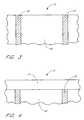
- FIG. 3is a partial cross-sectional view of a partially fabricated integrated circuit (IC), showing a conventional insulating filler material and conductive contacts;
- FIG. 4shows the IC of FIG. 3 after deposition of silicon hydroxide layer incorporating carbon
- FIG. 5shows the IC of FIG. 4 after a post-deposition treatment, thus forming an interlevel dielectric (ILD);
- ILDinterlevel dielectric
- FIG. 6shows the IC of FIG. 5 after a patterning and etch step to define trenches in the ILD
- FIG. 7shows the IC of FIG. 6 after a metal is deposited into the trenches and over the remaining ILD;
- FIG. 8shows the IC of FIG. 7 after the metal has been planarized to the top surface of the ILD, thereby isolating the metal runners within the trenches;
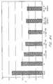
- FIG. 9Ashows the dielectric constants of materials form by prior art processes and processes in accordance with the preferred embodiments
- FIG. 9Bshows is a graph illustrating the dielectric constants of various materials, including low k materials formed in accordance with the preferred embodiments, as a function of anneal temperature
- FIG. 10is a partial cross-sectional view of a partially fabricated integrated circuit (IC), showing a conventional insulating filler material underlying a low k dielectric layer having trenches etched therein, in accordance with a dual damascene embodiment;
- ICintegrated circuit
- FIG. 11shows the IC of FIG. 10 after contact vias have been formed through the floor of the trenches
- FIG. 12is a partial cross-section view of a partially fabricated integrated circuit (IC), showing a first metal layer which has been patterned and etched into metal lines over an insulating material, in accordance with a gap fill integration embodiment;
- ICintegrated circuit
- FIG. 13shows the IC of FIG. 12 after deposition of a low k material, in accordance with the preferred embodiments
- FIG. 14shows the IC of FIG. 13 after planarizing the low k material and forming a contact opening therethrough;
- FIG. 15shows the IC of FIG. 14 after deposition of a second metal layer over the low k material and into the contact opening;
- FIG. 16is a partial cross-sectional view of an insulating spacer over an electrode or metal layer, formed in accordance with an embodiment of the invention.
- interlevel dielectricused to isolate metal lines or runners in an integrated circuit.
- ILDinterlevel dielectric
- the preferred processes and materialsalso have particular utility for front-end processes in IC fabrication, such as for shallow trench isolation, gate spacers, buried digit line spacers, etc., as is discussed further below.
- front-end processes in IC fabricationsuch as for shallow trench isolation, gate spacers, buried digit line spacers, etc., as is discussed further below.
- the skilled artisanwill recognize applications for the materials and methods disclosed herein whenever isolation with materials of low dielectric constant is desirable.
- FIG. 1illustrates a method of forming low dielectric material as an ILD.
- An organosilaneparticularly methylsilane (SiH 3 CH 3 )
- Si(OH) 4silicon hydroxide
- This layeris then treated to drive off water and form a stable low dielectric material suitable for electrical isolation in dense ICs.
- FIG. 1also shows a conventional post-deposition treatment of the deposited layer.
- the treatmentcomprises plasma enhanced chemical vapor deposition (PECVD) of a cap layer by reaction of silane and N 2 O in a plasma reactor, forming silicon oxynitride (SiO x N y ). These layers are then annealed in a nitrogen gas (N 2 ) environment at a temperature of about 450° C. This process drives off water in the deposited layer, forming an oxide-like layer while the SiO x N y seals the underlying layer against water incorporation.
- PECVDplasma enhanced chemical vapor deposition
- N 2nitrogen gas
- the relatively low anneal temperatureis compatible with conventional metals such as aluminum, which melt at relatively low temperatures.
- the cap layerhas a higher dielectric constant than the underlying low k material, such that an ILD incorporating both layers has a higher effective dielectric constant than the low k material alone.
- the advantage of the low dielectric constant materialis not fully realized.
- the cap layerin a damascene or dual damascene metallization process, the cap layer generally remains after metal polishing and the insulating material between metal layers has a higher overall dielectric constant.
- cap and low k layersetch or polish at different rates, and planarization of the resulting ILD is difficult to control and stop at a desired depth.
- planarizationis generally necessary where metallization is accomplished by gap fill integration, whereby metal is first deposited and etched, and the ILD deposited thereover.
- gap fill integrationwhereby metal is first deposited and etched, and the ILD deposited thereover.
- the skilled artisanwill recognize several other situations in which a uniform etch rate through a low k insulating material is desirable.
- FIG. 2thus illustrates an improved method of forming a low dielectric constant (low k) material, without the disadvantages of the above-described conventional post-deposition treatment.
- an organosilanereacts to form silicon hydroxide (also known as silanol or “flowfill oxide”), incorporating carbon.
- this depositionis followed by a plasma treatment and a thermal anneal.
- one or more substratesare loaded into a conventional chemical vapor deposition (CVD) reaction chamber.
- the substratesare typically partially fabricated integrated circuits, as will be apparent from the discussion below of FIGS. 3 to 8 .
- the skilled artisanwill recognize, however, that other means can be used to form the preferred silicon hydroxide incorporating carbon.
- the organosilanepreferably reacts with an oxygen source gas at the substrate surface.
- the organosilanepreferably comprises an alkyl silane, and most preferably comprises methylsilane (CH 3 SiH 3 ), while the oxidizing source most preferably comprises hydrogen peroxide.
- CH 3 SiH 3methylsilane
- the oxidizing sourcemost preferably comprises hydrogen peroxide.
- reactantscan result in a silicon hydroxide layer incorporating carbon.
- dimethylsilane ((CH 3 ) 2 SiH 2 ) and trimethylsilane ((CH 3 ) 3 SiH)can also react to form the desired layer.
- Methylsilaneis introduced into the chamber at a flow rate of about 50 sccm to 300 sccm, and preferably at a rate of 80 sccm to 150 sccm.
- Hydrogen peroxide from a liquid sourceis vaporized and delivered to the reaction chamber at a rate of 0.3 gram per minute (g/min) to 1 g/min, and preferably at a rate of 0.5 g/min to 0.75 g/min.
- the chamber pressureis preferably maintained at between about 400 mTorr and 1.5 Torr; and the substrate temperature is kept at about ⁇ 5° C.
- the methylsilane and hydrogen peroxidereact at the substrate surface to form silicon hydroxide or silanol (Si(OH) 4 ) layer, such as the layer 14 shown in FIG. 4, incorporating carbon in the form of methyl groups (CH 3 ).
- the reactionis thus of the form:
- the deposited productis predominantly Si(OH) 4 .
- the given productsare is deposited onto the substrate(s). It will be understood that the reaction will also produce volatile by-products such as H 2 , H 2 O, CO, CO 2 , etc., depending upon the properties of reactants and reaction conditions. Such by-products are carried off in the exhaust.
- Plasma treatmentrefers to a plasma process which does not deposit an appreciable layer over the silicon hydroxide layer.
- the plasma treatmentpreferably includes an oxygen component therein, preferably from source gases such as O 2 , O 3 , N 2 O, N 2 O/N 2 , or combinations thereof.
- the plasma treatmentis maintained for between about 5 seconds and 90 seconds, more preferably between about 30 seconds and 60 seconds.
- N 2 Owas provided at a rate of between about 100 sccm and 5,000 sccm, preferably 2,000 sccm, while N 2 was provided at a rate of 100 sccm to 5,000 sccm, preferably about 1,000 sccm.
- RF power sufficient to disassociate the constituent gaseswas applied to the electrodes of a plasma reactor.
- RF powerfor the plasma module of a Planner 200TM cluster tool, commercially available from Trikon Technologies in Bristol, U.K., RF power of between about 0.1 kW and 1 kW, more preferably about 0.5 kW will ionize the N 2 O/N 2 gas.
- ionizing powercan be coupled to the gas by way of microwave plasma or inductively coupled plasma as well.
- Pressure in the chambershould be maintained between about 300 mTorr and 1,500 mTorr, preferably about 750 mTorr.
- O 2 plasmawas applied.
- Oxygenis flowed into the above noted plasma module at a rate of between about 100 sccm and 1,000 sccm, more preferably between about 400 sccm and 600 sccm, while RF power in the range of 0.1 kW to 1 kW, and more preferably about 0.5 kW was applied to the electrodes.
- the chamber pressurecan be as described with respect to the N 2 O/N 2 embodiment described above. The skilled artisan will recognize different powers and pressures can be arranged to dissociate the reactant gases in different reactor configurations.
- the treated layeris preferably subjected to a thermal anneal, preferably at close to atmospheric pressure in a non-reactive ambient (e.g., N 2 O, N 2 , O 2 , O 3 , etc.).
- the thermal annealis a high temperature anneal, wherein the substrate is preferably heated to higher than about 400° C. and lower than about 800° C. More preferably, the substrate is annealed at about 500° C. to 700° C., and more preferably at 500° C. to 600° C., depending on the particular application for the low k material.
- the annealcan be maintained for between about 5 seconds and 3 minutes, while a furnace anneal can be maintained for between about 5 minutes and 40 minutes, more preferably between about 20 minutes and 30 minutes.
- the plasma treatmentcan be performed simultaneously with the high temperature anneal.
- the substrate on which the silicon hydroxide is formedcan be subjected to thermal processing during the plasma treatment.
- the pedestalcan include resistive heating elements, or the reactor can include radiant heaters outside transparent chamber walls, as will be understood by the skilled artisan.
- the plasma treatment described abovecan be employed without the high temperature anneal. This process is preferable in back end fabrication processes, during which the in-process IC already includes conventional metals which would otherwise melt if exposed to the high temperature anneal.
- the post-deposition treatmentdrives water out of the silanol, leaving a polysiloxane network incorporating carbon-to-silicon bonding.
- the materialexhibits many characteristics similar to those of silicon dioxide, but with a lower dielectric constant.
- the dielectric constant of the preferred polysiloxane networkis less than about 3.5, more preferably less than about 3.2, and most preferably less than about 3.0.
- FIG. 9Ais a bar chart illustrating dielectric constants of materials made from various fabrication processes. As is apparent, each of the described plasma treatment and high temperature anneal independently lower the dielectric constant of the treated silicon hydroxide, relative to conventional materials or processes. As shown, carbon-doped oxide formed by decomposing tetraethylorthosilicate (TEOS) exhibits a dielectric constant of about 4.25. “Flowfill” oxide (Si(OH) 4 without carbon), designated as “FF” in FIG. 9A, has a dielectric constant of about 3.6. Silicon hydroxide treated with a post-deposition cap layer followed by 400° C. anneal results in a lower dielectric constant of about 3.4.
- TEOStetraethylorthosilicate
- Such a processis particularly compatible with damascene processes (in which the cap layer need not be planarized away) and high temperature metallization such as CVD titanium or titanium silicide deposition (where the high temperature anneal will not harm previously deposited metal layers).
- high temperature metallizationsuch as CVD titanium or titanium silicide deposition (where the high temperature anneal will not harm previously deposited metal layers).
- PECVD SiO x N ycan be employed, as described above.
- Use of a cap layerincreases the effective k for the ILD above the values given here.
- FIG. 9Bgraphically shows the relation of the dielectric constant of the preferred low k material to anneal temperature. While temperatures higher than 400° C. resulted in lowering the dielectric constant in general, temperatures higher than 800° C. were found to result in loss of the carbon content in the ILD. Accordingly, as noted above, anneal temperature is preferably between about 450° C. and 800° C. More preferably, the substrate is annealed at about 500° C. to 700° C., and more preferably at 500° C. to 600° C., depending on the particular application for the low k material.
- STIshallow-trench isolation
- sidewall spacers used to isolate gatescan each be fabricated using the low k material disclosed herein with the preferred high temperature anneals.
- high temperature processingtends to follow formation of these structures at any rate, such that previously fabricated structures are capable of withstanding relatively high temperature cycling.
- continued scaling at today's ratemakes it ever more important that such front-end isolation elements have lower dielectric constants for reducing parasitic capacitance.
- lowering of the dielectric constantcan also be accomplished by plasma treatment, within the meaning of the present application, without the need for a high temperature anneal.
- an N 2 O/N 2 plasma post-deposition plasma treatmentresulted in a material having a dielectric constant of about 3.2, while the O 2 plasma exhibited a slightly lower dielectric constant (about 3.15) than that of the N 2 O/N 2 treatment.
- Such processesare particularly desirable in most back-end fabrication processes, where thermal budgets are reduced due to the presence of melting point metals in the partially fabricated integrated circuit.
- Plasma treatment without a cap layeris also particularly desirable in front-end processes, such as forming gate or digit line spacers, whether or not a high temperature anneal is also employed. For such applications, thinner films are required due to scaled circuit design.
- Plasma treatment in place of cap layer depositionenables realizing the full advantage of the lower k material, rather than the higher effective k produced by the cap layer.
- FIGS. 3 through 8illustrate use of the above-described low k material as an interlevel dielectric (ILD) in an exemplary metallization process.
- the illustrated processis known as a “damascene” process in the art of IC fabrication.
- FIG. 3shows a partially fabricated workpiece or substrate assembly 5 , including conventional IC isolation material, such as boron phosphorous silicate glass (BPSG), forming an insulating layer 10 .
- the insulating layer 10overlies a semiconductor substrate in which electrical devices are formed.
- the substratetypically comprises a silicon wafer or layer of epitaxial silicon.
- a plurality of contacts 12have been previously formed, extending downwardly through the insulating layer 10 to contact lower metal layers or active areas within the substrate.
- An exemplary contact 12 materialcomprises a tungsten (W) plug.
- the substrate 5is placed in a suitable processing chamber.
- the chambercontains a gas inlet to allow reaction gases, preferably methylsilane and hydrogen peroxide, to enter into the chamber.
- the gasesare preferably not premixed before introduction into the chamber.
- the chamber pressure and gas flow ratescan be as described above.
- the methylsilane and hydrogen peroxidereact to form a layer 14 of silicon hydroxide or silanol (Si(OH) 4 ) incorporating carbon.
- Si(OH) 4silicon hydroxide or silanol
- the layer 14is treated in accordance with the preferred embodiments to form a polysiloxane network.
- the treatmentmost preferably comprises a plasma treatment followed by a high temperature anneal, without formation of a cap layer.
- the low k ILD 16is then etched to form trenches 17 in a desired wiring pattern.
- the trenchescan be defined by depositing a photosensitive material (resist), patterning and developing the resist in accordance with conventional photolithographic techniques, and etching through the resultant mask.
- the low k dielectric material formed by the preferred processis chemically very similar to silicon dioxide. Accordingly, standard oxide etch chemistries, such as fluorocarbon plasma etches, can be used to etch the trenches into the low k dielectric material of the ILD 16 .
- etch chemistriescan include CFH 3 CF 2 H 2 , CF 3 H, etc.
- the trenches 17 thus formedexpose the previously formed contacts 12 , as shown. The etch may be timed to extend through the thickness of the ILD 16 or optical end stop technology can be employed. In either case, the above-described selective etch chemistry minimizes consumption of the underlying insulating layer 10 .
- a conductive layer 18is then deposited over the ILD 16 and into the trenches 17 .
- the wiring material 18comprises a metal, and is an aluminum/copper alloy in the illustrated embodiment.
- the conductive layer 18can be deposited by CVD, PECVD, sputtering, evaporation and the like.
- the metal layer 18is then etched or polished back to the surface of the ILD 16 , leaving metal runners or wires 20 within the trenches.
- the etch back processleaves the runners 20 electrically isolated from one another for proper circuit operation.
- the space between the wires 20is filled with the low k dielectric material 16 , such that parasitic capacitance between the lines 20 is minimized. While etch back can be achieve by numerous processes known in the art, preferably chemical mechanical planarization (CMP) is used, stopping on the ILD 16 , as will be understood by the skilled artisan.
- CMPchemical mechanical planarization
- FIGS. 10 and 11illustrate two steps in that process.
- elements similar to those of the previous embodimentwill be referred by like reference numerals, with the addition of a prime symbol (′) thereafter.
- FIG. 10a patterned ILD 16 ′ is illustrated over an insulating layer 10 ′, such as BPSG.
- the structure of FIG. 10is similar to that of FIG. 6, with the ILD 16 ′ formed in accordance with the preferred deposition and post-deposition process described above.
- Trenches 17 ′have also been etched through the ILD 16 ′ in a wiring pattern determined by circuit design and imparted to the ILD by photolithographic and etch techniques.
- contactshave not yet been formed through the insulating layer 10 ′ to underlying circuit elements (e.g., lower metal layers or electrical devices within the substrate). Rather, such contacts are made after the trenches 17 ′ for metal runners have been formed.
- the waferis again masked and contact vias 22 ′ are etched, extending from the floor of the trenches 17 ′ downwardly to expose a conductive element below (not shown).
- metalcan thereafter be deposited into the contact vias 22 ′ and metal trenches 17 ′ at the same time.
- the depositionblankets the entire wafer and is followed by an etch back to the top of the ILD 16 ′, preferably by CMP.
- the integrated circuitcan then be completed, for example, by the addition of further wiring layers (if necessary) and final passivation.
- dual damascene metallizationemploys a high temperature step to deposit metal with high conformality to fill the high-aspect ratio contact vias within trenches.
- TiSi 2requires either a silicidation anneal (self-aligned silicide) and/or a grain reorientation anneal.
- CVD Ti depositionis generally conducted at high temperatures. In either case, processes are conducted at greater than about 600° C. These high temperature steps can serve as the high temperature anneal for the low k material, thereby requiring only one anneal step to produce a low k process. In contrast, other known low k materials cannot withstand such high temperature processing without degradation resulting in a higher dielectric constant.
- the preferred process of forming a low kdemonstrates similar advantages when used between metal layers in a gap fill integration process.
- elements similar to those of the previous embodimentswill be referred by like reference numerals, with the addition of a double prime (′′) thereafter.
- contacts 12 ′′have been formed in an insulating layer 10 ′′, while metal lines 20 ′′ have been patterned above the insulating layer 10 ′′ in a conventional metallization process.
- a blanket metal layeris deposited, then patterned and etched by conventional photolithographic techniques.
- a low k material 16 ′′is formed over the metal lines 20 ′′, in accordance with the processes set forth above.
- a precursor materialis deposited and subjected to a plasma treatment to form the low k material 16 ′′.
- the low k material 16 ′′can be optionally thermally annealed immediately after deposition.
- the material 16 ′′can be subjected to anneal in a later process, obviating the separate anneal. Because the material 16 ′′ flows between and fills spaces between the previously defined metal lines 20 ′′, this process can be referred to as a “gap fill integration” process.
- the low k material 16 ′′is then planarized and contacts 17 ′′ (one shown) are etched therethrough.
- standard oxide etch chemistriessuch as fluorocarbon plasma etches, can be used to etch through the low k material 16 ′′.
- a second metal or metal 2 layer 31is then deposited over the low k material 16 ′′ and into the contacts 17 ′′.
- the contact 17 ′′is difficult to fill with standard physical vapor deposition (PVD) techniques.
- the second metal layer 31is preferably deposited by a hot metal process, such as by deposition of aluminum at greater than about 550° C.
- the metal depositionadvantageously serves as an anneal to further lower the dielectric constant of the low k material 16 ′′.
- the gap fill metallization contextpresents yet another context in which low k materials in accordance with the invention can be integrated into process flows with high temperature steps without degradation and indeed, with advantageous lowering of the dielectric constant.
- the preferred low k materialcan also be used to isolate electrical devices in front-end processes.
- transistor active areas within the substratecan be separated by etching trenches into the substrate and filling the trenches with the preferred low k material, in a shallow trench isolation (STI) process.
- STIshallow trench isolation
- the low k materialcan be subjected to temperatures at the upper end of the preferred ranges for the high temperature anneal.
- the conductorcomprises a transistor gate electrode 30 overlying a silicon substrate 32 , and particularly a channel region 34 of the substrate.
- the channel 34is defined between active areas 36 of the substrate.
- the transistor gate 30also serves a word line for the array.
- the conductorcan comprise a digit line in a DRAM.
- the conductoris protected and electrically isolated from surrounding electrical layers by a cap spacer 38 and a pair of sidewall spacers 40 , each constructed of the preferred low k material.
- the sidewall spacers 40can be formed by formation of a blanket layer of the low k material, followed by an anisotropic etch, which etches horizontal surfaces of the blanket layer while leaving the vertical spacers 40 .
- An insulating filler layer 42e.g., BPSG
- a conductive contact 44is formed to electrically connect one of the active areas 36 (e.g., transistor drain region) to higher wiring layers.
- conductive elementssuch as the contact 44 and the gate 30 become closer to one another, tending to exhibit parasitic capacitance across the insulating spacers 40 which ties up charge carriers and slows circuit operation.
- the contact 44actually encroaches on the sidewall spacers 40 , such that opposite sides of a spacer 40 are directly contacted by conductive elements 30 and 44 . Accordingly, the low k material is particularly advantageous in reducing such parasitic capacitance across insulating electrode spacers.
- circuit designsemploy buried digit lines, formed beneath the capacitor of a memory cell.
- the digit linemust also be insulated from conductive elements crowding the memory cell.
- sidewall spacers employing the preferred low k materialwill also be particularly advantageous for protecting such buried digit lines as well.
- the low k material in any of the above-noted embodimentscan be formed without a cap layer. Accordingly, the low k material can form the only insulating material between conductive elements in an integrated circuit at at least one point, since no cap layer is required to reduce the dielectric constant.
- the polysilicon contact 44directly contacts a low k sidewall spacer 40 near the substrate 32
- the gate electrode 30directly contacts the opposite side of the spacer 40 .
- opposite sides of an ILD segment 16are directly contacted by metal runners 20 .
Landscapes
- Chemical & Material Sciences (AREA)
- Engineering & Computer Science (AREA)
- Physics & Mathematics (AREA)
- Condensed Matter Physics & Semiconductors (AREA)
- General Physics & Mathematics (AREA)
- Manufacturing & Machinery (AREA)
- Computer Hardware Design (AREA)
- Microelectronics & Electronic Packaging (AREA)
- Power Engineering (AREA)
- Chemical Kinetics & Catalysis (AREA)
- Organic Chemistry (AREA)
- General Chemical & Material Sciences (AREA)
- Materials Engineering (AREA)
- Mechanical Engineering (AREA)
- Metallurgy (AREA)
- Plasma & Fusion (AREA)
- Inorganic Chemistry (AREA)
- Internal Circuitry In Semiconductor Integrated Circuit Devices (AREA)
- Formation Of Insulating Films (AREA)
- Element Separation (AREA)
Abstract
Description
Claims (9)
Priority Applications (1)
| Application Number | Priority Date | Filing Date | Title |
|---|---|---|---|
| US10/033,656US6835995B2 (en) | 1998-09-03 | 2001-12-27 | Low dielectric constant material for integrated circuit fabrication |
Applications Claiming Priority (2)
| Application Number | Priority Date | Filing Date | Title |
|---|---|---|---|
| US09/146,397US6383951B1 (en) | 1998-09-03 | 1998-09-03 | Low dielectric constant material for integrated circuit fabrication |
| US10/033,656US6835995B2 (en) | 1998-09-03 | 2001-12-27 | Low dielectric constant material for integrated circuit fabrication |
Related Parent Applications (1)
| Application Number | Title | Priority Date | Filing Date |
|---|---|---|---|
| US09/146,397DivisionUS6383951B1 (en) | 1998-09-03 | 1998-09-03 | Low dielectric constant material for integrated circuit fabrication |
Publications (2)
| Publication Number | Publication Date |
|---|---|
| US20020105084A1 US20020105084A1 (en) | 2002-08-08 |
| US6835995B2true US6835995B2 (en) | 2004-12-28 |
Family
ID=22517186
Family Applications (2)
| Application Number | Title | Priority Date | Filing Date |
|---|---|---|---|
| US09/146,397Expired - Fee RelatedUS6383951B1 (en) | 1998-09-03 | 1998-09-03 | Low dielectric constant material for integrated circuit fabrication |
| US10/033,656Expired - LifetimeUS6835995B2 (en) | 1998-09-03 | 2001-12-27 | Low dielectric constant material for integrated circuit fabrication |
Family Applications Before (1)
| Application Number | Title | Priority Date | Filing Date |
|---|---|---|---|
| US09/146,397Expired - Fee RelatedUS6383951B1 (en) | 1998-09-03 | 1998-09-03 | Low dielectric constant material for integrated circuit fabrication |
Country Status (2)
| Country | Link |
|---|---|
| US (2) | US6383951B1 (en) |
| JP (2) | JP3716404B2 (en) |
Cited By (153)
| Publication number | Priority date | Publication date | Assignee | Title |
|---|---|---|---|---|
| US20070202640A1 (en)* | 2006-02-28 | 2007-08-30 | Applied Materials, Inc. | Low-k spacer integration into CMOS transistors |
| US20090001581A1 (en)* | 2007-06-28 | 2009-01-01 | Eun Soo Kim | Metal line of semiconductor device and method of forming the same |
| US8343307B2 (en) | 2004-02-26 | 2013-01-01 | Applied Materials, Inc. | Showerhead assembly |
| US8679983B2 (en) | 2011-09-01 | 2014-03-25 | Applied Materials, Inc. | Selective suppression of dry-etch rate of materials containing both silicon and nitrogen |
| US8679982B2 (en) | 2011-08-26 | 2014-03-25 | Applied Materials, Inc. | Selective suppression of dry-etch rate of materials containing both silicon and oxygen |
| US8765574B2 (en) | 2012-11-09 | 2014-07-01 | Applied Materials, Inc. | Dry etch process |
| US8771539B2 (en) | 2011-02-22 | 2014-07-08 | Applied Materials, Inc. | Remotely-excited fluorine and water vapor etch |
| US8801952B1 (en) | 2013-03-07 | 2014-08-12 | Applied Materials, Inc. | Conformal oxide dry etch |
| US8808563B2 (en) | 2011-10-07 | 2014-08-19 | Applied Materials, Inc. | Selective etch of silicon by way of metastable hydrogen termination |
| US8895449B1 (en) | 2013-05-16 | 2014-11-25 | Applied Materials, Inc. | Delicate dry clean |
| US8921234B2 (en) | 2012-12-21 | 2014-12-30 | Applied Materials, Inc. | Selective titanium nitride etching |
| US8927390B2 (en) | 2011-09-26 | 2015-01-06 | Applied Materials, Inc. | Intrench profile |
| US8951429B1 (en) | 2013-10-29 | 2015-02-10 | Applied Materials, Inc. | Tungsten oxide processing |
| US8956980B1 (en) | 2013-09-16 | 2015-02-17 | Applied Materials, Inc. | Selective etch of silicon nitride |
| US8969212B2 (en) | 2012-11-20 | 2015-03-03 | Applied Materials, Inc. | Dry-etch selectivity |
| US8975152B2 (en) | 2011-11-08 | 2015-03-10 | Applied Materials, Inc. | Methods of reducing substrate dislocation during gapfill processing |
| US8980763B2 (en) | 2012-11-30 | 2015-03-17 | Applied Materials, Inc. | Dry-etch for selective tungsten removal |
| US8999856B2 (en) | 2011-03-14 | 2015-04-07 | Applied Materials, Inc. | Methods for etch of sin films |
| US9023734B2 (en) | 2012-09-18 | 2015-05-05 | Applied Materials, Inc. | Radical-component oxide etch |
| US9023732B2 (en) | 2013-03-15 | 2015-05-05 | Applied Materials, Inc. | Processing systems and methods for halide scavenging |
| US9034770B2 (en) | 2012-09-17 | 2015-05-19 | Applied Materials, Inc. | Differential silicon oxide etch |
| US9040422B2 (en) | 2013-03-05 | 2015-05-26 | Applied Materials, Inc. | Selective titanium nitride removal |
| US9064816B2 (en) | 2012-11-30 | 2015-06-23 | Applied Materials, Inc. | Dry-etch for selective oxidation removal |
| US9064815B2 (en) | 2011-03-14 | 2015-06-23 | Applied Materials, Inc. | Methods for etch of metal and metal-oxide films |
| US9111877B2 (en) | 2012-12-18 | 2015-08-18 | Applied Materials, Inc. | Non-local plasma oxide etch |
| US9117855B2 (en) | 2013-12-04 | 2015-08-25 | Applied Materials, Inc. | Polarity control for remote plasma |
| US9114438B2 (en) | 2013-05-21 | 2015-08-25 | Applied Materials, Inc. | Copper residue chamber clean |
| US9132436B2 (en) | 2012-09-21 | 2015-09-15 | Applied Materials, Inc. | Chemical control features in wafer process equipment |
| US9136273B1 (en) | 2014-03-21 | 2015-09-15 | Applied Materials, Inc. | Flash gate air gap |
| US9159606B1 (en) | 2014-07-31 | 2015-10-13 | Applied Materials, Inc. | Metal air gap |
| US9165786B1 (en) | 2014-08-05 | 2015-10-20 | Applied Materials, Inc. | Integrated oxide and nitride recess for better channel contact in 3D architectures |
| US9190293B2 (en) | 2013-12-18 | 2015-11-17 | Applied Materials, Inc. | Even tungsten etch for high aspect ratio trenches |
| US9236265B2 (en) | 2013-11-04 | 2016-01-12 | Applied Materials, Inc. | Silicon germanium processing |
| US9236266B2 (en) | 2011-08-01 | 2016-01-12 | Applied Materials, Inc. | Dry-etch for silicon-and-carbon-containing films |
| US9245762B2 (en) | 2013-12-02 | 2016-01-26 | Applied Materials, Inc. | Procedure for etch rate consistency |
| US9263278B2 (en) | 2013-12-17 | 2016-02-16 | Applied Materials, Inc. | Dopant etch selectivity control |
| US9269590B2 (en) | 2014-04-07 | 2016-02-23 | Applied Materials, Inc. | Spacer formation |
| US9287134B2 (en) | 2014-01-17 | 2016-03-15 | Applied Materials, Inc. | Titanium oxide etch |
| US9287095B2 (en) | 2013-12-17 | 2016-03-15 | Applied Materials, Inc. | Semiconductor system assemblies and methods of operation |
| US9293568B2 (en) | 2014-01-27 | 2016-03-22 | Applied Materials, Inc. | Method of fin patterning |
| US9299538B2 (en) | 2014-03-20 | 2016-03-29 | Applied Materials, Inc. | Radial waveguide systems and methods for post-match control of microwaves |
| US9299575B2 (en) | 2014-03-17 | 2016-03-29 | Applied Materials, Inc. | Gas-phase tungsten etch |
| US9299582B2 (en) | 2013-11-12 | 2016-03-29 | Applied Materials, Inc. | Selective etch for metal-containing materials |
| US9299583B1 (en) | 2014-12-05 | 2016-03-29 | Applied Materials, Inc. | Aluminum oxide selective etch |
| US9299537B2 (en) | 2014-03-20 | 2016-03-29 | Applied Materials, Inc. | Radial waveguide systems and methods for post-match control of microwaves |
| US9309598B2 (en) | 2014-05-28 | 2016-04-12 | Applied Materials, Inc. | Oxide and metal removal |
| US9324576B2 (en) | 2010-05-27 | 2016-04-26 | Applied Materials, Inc. | Selective etch for silicon films |
| US9343272B1 (en) | 2015-01-08 | 2016-05-17 | Applied Materials, Inc. | Self-aligned process |
| US9349605B1 (en) | 2015-08-07 | 2016-05-24 | Applied Materials, Inc. | Oxide etch selectivity systems and methods |
| US9355856B2 (en) | 2014-09-12 | 2016-05-31 | Applied Materials, Inc. | V trench dry etch |
| US9355862B2 (en) | 2014-09-24 | 2016-05-31 | Applied Materials, Inc. | Fluorine-based hardmask removal |
| US9362130B2 (en) | 2013-03-01 | 2016-06-07 | Applied Materials, Inc. | Enhanced etching processes using remote plasma sources |
| US9368364B2 (en) | 2014-09-24 | 2016-06-14 | Applied Materials, Inc. | Silicon etch process with tunable selectivity to SiO2 and other materials |
| US9373522B1 (en) | 2015-01-22 | 2016-06-21 | Applied Mateials, Inc. | Titanium nitride removal |
| US9373517B2 (en) | 2012-08-02 | 2016-06-21 | Applied Materials, Inc. | Semiconductor processing with DC assisted RF power for improved control |
| US9378978B2 (en) | 2014-07-31 | 2016-06-28 | Applied Materials, Inc. | Integrated oxide recess and floating gate fin trimming |
| US9378969B2 (en) | 2014-06-19 | 2016-06-28 | Applied Materials, Inc. | Low temperature gas-phase carbon removal |
| US9385028B2 (en) | 2014-02-03 | 2016-07-05 | Applied Materials, Inc. | Air gap process |
| US9390937B2 (en) | 2012-09-20 | 2016-07-12 | Applied Materials, Inc. | Silicon-carbon-nitride selective etch |
| US9396989B2 (en) | 2014-01-27 | 2016-07-19 | Applied Materials, Inc. | Air gaps between copper lines |
| US9406523B2 (en) | 2014-06-19 | 2016-08-02 | Applied Materials, Inc. | Highly selective doped oxide removal method |
| US9425058B2 (en) | 2014-07-24 | 2016-08-23 | Applied Materials, Inc. | Simplified litho-etch-litho-etch process |
| US9449846B2 (en) | 2015-01-28 | 2016-09-20 | Applied Materials, Inc. | Vertical gate separation |
| US9478432B2 (en) | 2014-09-25 | 2016-10-25 | Applied Materials, Inc. | Silicon oxide selective removal |
| US9496167B2 (en) | 2014-07-31 | 2016-11-15 | Applied Materials, Inc. | Integrated bit-line airgap formation and gate stack post clean |
| US9493879B2 (en) | 2013-07-12 | 2016-11-15 | Applied Materials, Inc. | Selective sputtering for pattern transfer |
| US9499898B2 (en) | 2014-03-03 | 2016-11-22 | Applied Materials, Inc. | Layered thin film heater and method of fabrication |
| US9502258B2 (en) | 2014-12-23 | 2016-11-22 | Applied Materials, Inc. | Anisotropic gap etch |
| US9553102B2 (en) | 2014-08-19 | 2017-01-24 | Applied Materials, Inc. | Tungsten separation |
| US9576809B2 (en) | 2013-11-04 | 2017-02-21 | Applied Materials, Inc. | Etch suppression with germanium |
| US9659753B2 (en) | 2014-08-07 | 2017-05-23 | Applied Materials, Inc. | Grooved insulator to reduce leakage current |
| US9691645B2 (en) | 2015-08-06 | 2017-06-27 | Applied Materials, Inc. | Bolted wafer chuck thermal management systems and methods for wafer processing systems |
| US9721789B1 (en) | 2016-10-04 | 2017-08-01 | Applied Materials, Inc. | Saving ion-damaged spacers |
| US9728437B2 (en) | 2015-02-03 | 2017-08-08 | Applied Materials, Inc. | High temperature chuck for plasma processing systems |
| US9741593B2 (en) | 2015-08-06 | 2017-08-22 | Applied Materials, Inc. | Thermal management systems and methods for wafer processing systems |
| US9768034B1 (en) | 2016-11-11 | 2017-09-19 | Applied Materials, Inc. | Removal methods for high aspect ratio structures |
| US9773648B2 (en) | 2013-08-30 | 2017-09-26 | Applied Materials, Inc. | Dual discharge modes operation for remote plasma |
| US9847289B2 (en) | 2014-05-30 | 2017-12-19 | Applied Materials, Inc. | Protective via cap for improved interconnect performance |
| US9865484B1 (en) | 2016-06-29 | 2018-01-09 | Applied Materials, Inc. | Selective etch using material modification and RF pulsing |
| US9881805B2 (en) | 2015-03-02 | 2018-01-30 | Applied Materials, Inc. | Silicon selective removal |
| US9885117B2 (en) | 2014-03-31 | 2018-02-06 | Applied Materials, Inc. | Conditioned semiconductor system parts |
| US9934942B1 (en) | 2016-10-04 | 2018-04-03 | Applied Materials, Inc. | Chamber with flow-through source |
| US9947549B1 (en) | 2016-10-10 | 2018-04-17 | Applied Materials, Inc. | Cobalt-containing material removal |
| US10026621B2 (en) | 2016-11-14 | 2018-07-17 | Applied Materials, Inc. | SiN spacer profile patterning |
| US10043684B1 (en) | 2017-02-06 | 2018-08-07 | Applied Materials, Inc. | Self-limiting atomic thermal etching systems and methods |
| US10043674B1 (en) | 2017-08-04 | 2018-08-07 | Applied Materials, Inc. | Germanium etching systems and methods |
| US10049891B1 (en) | 2017-05-31 | 2018-08-14 | Applied Materials, Inc. | Selective in situ cobalt residue removal |
| US10062579B2 (en) | 2016-10-07 | 2018-08-28 | Applied Materials, Inc. | Selective SiN lateral recess |
| US10062575B2 (en) | 2016-09-09 | 2018-08-28 | Applied Materials, Inc. | Poly directional etch by oxidation |
| US10062585B2 (en) | 2016-10-04 | 2018-08-28 | Applied Materials, Inc. | Oxygen compatible plasma source |
| US10062587B2 (en) | 2012-07-18 | 2018-08-28 | Applied Materials, Inc. | Pedestal with multi-zone temperature control and multiple purge capabilities |
| US10128086B1 (en) | 2017-10-24 | 2018-11-13 | Applied Materials, Inc. | Silicon pretreatment for nitride removal |
| US10163696B2 (en) | 2016-11-11 | 2018-12-25 | Applied Materials, Inc. | Selective cobalt removal for bottom up gapfill |
| US10170336B1 (en) | 2017-08-04 | 2019-01-01 | Applied Materials, Inc. | Methods for anisotropic control of selective silicon removal |
| US10170282B2 (en) | 2013-03-08 | 2019-01-01 | Applied Materials, Inc. | Insulated semiconductor faceplate designs |
| US10224210B2 (en) | 2014-12-09 | 2019-03-05 | Applied Materials, Inc. | Plasma processing system with direct outlet toroidal plasma source |
| US10242908B2 (en) | 2016-11-14 | 2019-03-26 | Applied Materials, Inc. | Airgap formation with damage-free copper |
| US10256079B2 (en) | 2013-02-08 | 2019-04-09 | Applied Materials, Inc. | Semiconductor processing systems having multiple plasma configurations |
| US10256112B1 (en) | 2017-12-08 | 2019-04-09 | Applied Materials, Inc. | Selective tungsten removal |
| US10283324B1 (en) | 2017-10-24 | 2019-05-07 | Applied Materials, Inc. | Oxygen treatment for nitride etching |
| US10283321B2 (en) | 2011-01-18 | 2019-05-07 | Applied Materials, Inc. | Semiconductor processing system and methods using capacitively coupled plasma |
| US10297458B2 (en) | 2017-08-07 | 2019-05-21 | Applied Materials, Inc. | Process window widening using coated parts in plasma etch processes |
| US10319739B2 (en) | 2017-02-08 | 2019-06-11 | Applied Materials, Inc. | Accommodating imperfectly aligned memory holes |
| US10319649B2 (en) | 2017-04-11 | 2019-06-11 | Applied Materials, Inc. | Optical emission spectroscopy (OES) for remote plasma monitoring |
| US10319600B1 (en) | 2018-03-12 | 2019-06-11 | Applied Materials, Inc. | Thermal silicon etch |
| US10354889B2 (en) | 2017-07-17 | 2019-07-16 | Applied Materials, Inc. | Non-halogen etching of silicon-containing materials |
| US10403507B2 (en) | 2017-02-03 | 2019-09-03 | Applied Materials, Inc. | Shaped etch profile with oxidation |
| US10431429B2 (en) | 2017-02-03 | 2019-10-01 | Applied Materials, Inc. | Systems and methods for radial and azimuthal control of plasma uniformity |
| US10468267B2 (en) | 2017-05-31 | 2019-11-05 | Applied Materials, Inc. | Water-free etching methods |
| US10490418B2 (en) | 2014-10-14 | 2019-11-26 | Applied Materials, Inc. | Systems and methods for internal surface conditioning assessment in plasma processing equipment |
| US10490406B2 (en) | 2018-04-10 | 2019-11-26 | Appled Materials, Inc. | Systems and methods for material breakthrough |
| US10497573B2 (en) | 2018-03-13 | 2019-12-03 | Applied Materials, Inc. | Selective atomic layer etching of semiconductor materials |
| US10504754B2 (en) | 2016-05-19 | 2019-12-10 | Applied Materials, Inc. | Systems and methods for improved semiconductor etching and component protection |
| US10504700B2 (en) | 2015-08-27 | 2019-12-10 | Applied Materials, Inc. | Plasma etching systems and methods with secondary plasma injection |
| US10522371B2 (en) | 2016-05-19 | 2019-12-31 | Applied Materials, Inc. | Systems and methods for improved semiconductor etching and component protection |
| US10541246B2 (en) | 2017-06-26 | 2020-01-21 | Applied Materials, Inc. | 3D flash memory cells which discourage cross-cell electrical tunneling |
| US10541184B2 (en) | 2017-07-11 | 2020-01-21 | Applied Materials, Inc. | Optical emission spectroscopic techniques for monitoring etching |
| US10546729B2 (en) | 2016-10-04 | 2020-01-28 | Applied Materials, Inc. | Dual-channel showerhead with improved profile |
| US10566206B2 (en) | 2016-12-27 | 2020-02-18 | Applied Materials, Inc. | Systems and methods for anisotropic material breakthrough |
| US10573527B2 (en) | 2018-04-06 | 2020-02-25 | Applied Materials, Inc. | Gas-phase selective etching systems and methods |
| US10573496B2 (en) | 2014-12-09 | 2020-02-25 | Applied Materials, Inc. | Direct outlet toroidal plasma source |
| US10593523B2 (en) | 2014-10-14 | 2020-03-17 | Applied Materials, Inc. | Systems and methods for internal surface conditioning in plasma processing equipment |
| US10593560B2 (en) | 2018-03-01 | 2020-03-17 | Applied Materials, Inc. | Magnetic induction plasma source for semiconductor processes and equipment |
| US10615047B2 (en) | 2018-02-28 | 2020-04-07 | Applied Materials, Inc. | Systems and methods to form airgaps |
| US10629473B2 (en) | 2016-09-09 | 2020-04-21 | Applied Materials, Inc. | Footing removal for nitride spacer |
| US10672642B2 (en) | 2018-07-24 | 2020-06-02 | Applied Materials, Inc. | Systems and methods for pedestal configuration |
| US10679870B2 (en) | 2018-02-15 | 2020-06-09 | Applied Materials, Inc. | Semiconductor processing chamber multistage mixing apparatus |
| US10699879B2 (en) | 2018-04-17 | 2020-06-30 | Applied Materials, Inc. | Two piece electrode assembly with gap for plasma control |
| US10727080B2 (en) | 2017-07-07 | 2020-07-28 | Applied Materials, Inc. | Tantalum-containing material removal |
| US10755941B2 (en) | 2018-07-06 | 2020-08-25 | Applied Materials, Inc. | Self-limiting selective etching systems and methods |
| US10854426B2 (en) | 2018-01-08 | 2020-12-01 | Applied Materials, Inc. | Metal recess for semiconductor structures |
| US10872778B2 (en) | 2018-07-06 | 2020-12-22 | Applied Materials, Inc. | Systems and methods utilizing solid-phase etchants |
| US10886137B2 (en) | 2018-04-30 | 2021-01-05 | Applied Materials, Inc. | Selective nitride removal |
| US10892198B2 (en) | 2018-09-14 | 2021-01-12 | Applied Materials, Inc. | Systems and methods for improved performance in semiconductor processing |
| US10903054B2 (en) | 2017-12-19 | 2021-01-26 | Applied Materials, Inc. | Multi-zone gas distribution systems and methods |
| US10920320B2 (en) | 2017-06-16 | 2021-02-16 | Applied Materials, Inc. | Plasma health determination in semiconductor substrate processing reactors |
| US10920319B2 (en) | 2019-01-11 | 2021-02-16 | Applied Materials, Inc. | Ceramic showerheads with conductive electrodes |
| US10943834B2 (en) | 2017-03-13 | 2021-03-09 | Applied Materials, Inc. | Replacement contact process |
| US10964512B2 (en) | 2018-02-15 | 2021-03-30 | Applied Materials, Inc. | Semiconductor processing chamber multistage mixing apparatus and methods |
| US11049755B2 (en) | 2018-09-14 | 2021-06-29 | Applied Materials, Inc. | Semiconductor substrate supports with embedded RF shield |
| US11062887B2 (en) | 2018-09-17 | 2021-07-13 | Applied Materials, Inc. | High temperature RF heater pedestals |
| US11121002B2 (en) | 2018-10-24 | 2021-09-14 | Applied Materials, Inc. | Systems and methods for etching metals and metal derivatives |
| US11239061B2 (en) | 2014-11-26 | 2022-02-01 | Applied Materials, Inc. | Methods and systems to enhance process uniformity |
| US11257693B2 (en) | 2015-01-09 | 2022-02-22 | Applied Materials, Inc. | Methods and systems to improve pedestal temperature control |
| US11276559B2 (en) | 2017-05-17 | 2022-03-15 | Applied Materials, Inc. | Semiconductor processing chamber for multiple precursor flow |
| US11276590B2 (en) | 2017-05-17 | 2022-03-15 | Applied Materials, Inc. | Multi-zone semiconductor substrate supports |
| US11328909B2 (en) | 2017-12-22 | 2022-05-10 | Applied Materials, Inc. | Chamber conditioning and removal processes |
| US11417534B2 (en) | 2018-09-21 | 2022-08-16 | Applied Materials, Inc. | Selective material removal |
| US11437242B2 (en) | 2018-11-27 | 2022-09-06 | Applied Materials, Inc. | Selective removal of silicon-containing materials |
| US11594428B2 (en) | 2015-02-03 | 2023-02-28 | Applied Materials, Inc. | Low temperature chuck for plasma processing systems |
| US11682560B2 (en) | 2018-10-11 | 2023-06-20 | Applied Materials, Inc. | Systems and methods for hafnium-containing film removal |
| US11721527B2 (en) | 2019-01-07 | 2023-08-08 | Applied Materials, Inc. | Processing chamber mixing systems |
| US12340979B2 (en) | 2017-05-17 | 2025-06-24 | Applied Materials, Inc. | Semiconductor processing chamber for improved precursor flow |
Families Citing this family (84)
| Publication number | Priority date | Publication date | Assignee | Title |
|---|---|---|---|---|
| US6287990B1 (en) | 1998-02-11 | 2001-09-11 | Applied Materials, Inc. | CVD plasma assisted low dielectric constant films |
| US6054379A (en) | 1998-02-11 | 2000-04-25 | Applied Materials, Inc. | Method of depositing a low k dielectric with organo silane |
| US6627532B1 (en) | 1998-02-11 | 2003-09-30 | Applied Materials, Inc. | Method of decreasing the K value in SiOC layer deposited by chemical vapor deposition |
| US6660656B2 (en) | 1998-02-11 | 2003-12-09 | Applied Materials Inc. | Plasma processes for depositing low dielectric constant films |
| US6303523B2 (en) | 1998-02-11 | 2001-10-16 | Applied Materials, Inc. | Plasma processes for depositing low dielectric constant films |
| US6593247B1 (en)* | 1998-02-11 | 2003-07-15 | Applied Materials, Inc. | Method of depositing low k films using an oxidizing plasma |
| US6274292B1 (en)* | 1998-02-25 | 2001-08-14 | Micron Technology, Inc. | Semiconductor processing methods |
| US7804115B2 (en)* | 1998-02-25 | 2010-09-28 | Micron Technology, Inc. | Semiconductor constructions having antireflective portions |
| US6800571B2 (en)* | 1998-09-29 | 2004-10-05 | Applied Materials Inc. | CVD plasma assisted low dielectric constant films |
| US6303972B1 (en) | 1998-11-25 | 2001-10-16 | Micron Technology, Inc. | Device including a conductive layer protected against oxidation |
| US7067861B1 (en)* | 1998-11-25 | 2006-06-27 | Micron Technology, Inc. | Device and method for protecting against oxidation of a conductive layer in said device |
| US6828683B2 (en)* | 1998-12-23 | 2004-12-07 | Micron Technology, Inc. | Semiconductor devices, and semiconductor processing methods |
| US8944070B2 (en) | 1999-04-07 | 2015-02-03 | Intuitive Surgical Operations, Inc. | Non-force reflecting method for providing tool force information to a user of a telesurgical system |
| US7067414B1 (en)* | 1999-09-01 | 2006-06-27 | Micron Technology, Inc. | Low k interlevel dielectric layer fabrication methods |
| KR100363081B1 (en)* | 1999-09-16 | 2002-11-30 | 삼성전자 주식회사 | Thin film formation apparatus |
| JP3615979B2 (en)* | 2000-01-18 | 2005-02-02 | 株式会社ルネサステクノロジ | Semiconductor device and manufacturing method thereof |
| US6440860B1 (en)* | 2000-01-18 | 2002-08-27 | Micron Technology, Inc. | Semiconductor processing methods of transferring patterns from patterned photoresists to materials, and structures comprising silicon nitride |
| JP4368498B2 (en)* | 2000-05-16 | 2009-11-18 | Necエレクトロニクス株式会社 | Semiconductor device, semiconductor wafer and manufacturing method thereof |
| US6762132B1 (en) | 2000-08-31 | 2004-07-13 | Micron Technology, Inc. | Compositions for dissolution of low-K dielectric films, and methods of use |
| US6472333B2 (en) | 2001-03-28 | 2002-10-29 | Applied Materials, Inc. | Silicon carbide cap layers for low dielectric constant silicon oxide layers |
| US7183201B2 (en)* | 2001-07-23 | 2007-02-27 | Applied Materials, Inc. | Selective etching of organosilicate films over silicon oxide stop etch layers |
| US6632735B2 (en) | 2001-08-07 | 2003-10-14 | Applied Materials, Inc. | Method of depositing low dielectric constant carbon doped silicon oxide |
| US6762127B2 (en)* | 2001-08-23 | 2004-07-13 | Yves Pierre Boiteux | Etch process for dielectric materials comprising oxidized organo silane materials |
| US6500770B1 (en)* | 2002-04-22 | 2002-12-31 | Taiwan Semiconductor Manufacturing Company, Ltd | Method for forming a multi-layer protective coating over porous low-k material |
| US6613637B1 (en)* | 2002-05-31 | 2003-09-02 | Lsi Logic Corporation | Composite spacer scheme with low overlapped parasitic capacitance |
| US6927178B2 (en)* | 2002-07-11 | 2005-08-09 | Applied Materials, Inc. | Nitrogen-free dielectric anti-reflective coating and hardmask |
| US7105460B2 (en)* | 2002-07-11 | 2006-09-12 | Applied Materials | Nitrogen-free dielectric anti-reflective coating and hardmask |
| US6806149B2 (en)* | 2002-09-26 | 2004-10-19 | Texas Instruments Incorporated | Sidewall processes using alkylsilane precursors for MOS transistor fabrication |
| US6770570B2 (en)* | 2002-11-15 | 2004-08-03 | Taiwan Semiconductor Manufacturing Company, Ltd. | Method of forming a semiconductor device with a substantially uniform density low-k dielectric layer |
| US7205248B2 (en)* | 2003-02-04 | 2007-04-17 | Micron Technology, Inc. | Method of eliminating residual carbon from flowable oxide fill |
| US7138158B2 (en)* | 2003-02-28 | 2006-11-21 | Intel Corporation | Forming a dielectric layer using a hydrocarbon-containing precursor |
| US6939817B2 (en)* | 2003-05-08 | 2005-09-06 | Micron Technology, Inc. | Removal of carbon from an insulative layer using ozone |
| US7033897B2 (en)* | 2003-10-23 | 2006-04-25 | Texas Instruments Incorporated | Encapsulated spacer with low dielectric constant material to reduce the parasitic capacitance between gate and drain in CMOS technology |
| US20060051966A1 (en)* | 2004-02-26 | 2006-03-09 | Applied Materials, Inc. | In-situ chamber clean process to remove by-product deposits from chemical vapor etch chamber |
| US9257302B1 (en) | 2004-03-25 | 2016-02-09 | Novellus Systems, Inc. | CVD flowable gap fill |
| US7524735B1 (en) | 2004-03-25 | 2009-04-28 | Novellus Systems, Inc | Flowable film dielectric gap fill process |
| US7582555B1 (en) | 2005-12-29 | 2009-09-01 | Novellus Systems, Inc. | CVD flowable gap fill |
| US7071093B2 (en) | 2004-03-26 | 2006-07-04 | Taiwan Semiconductor Manufacturing Company, Ltd. | Integrated treatment method for obtaining robust low dielectric constant materials |
| US7018941B2 (en) | 2004-04-21 | 2006-03-28 | Applied Materials, Inc. | Post treatment of low k dielectric films |
| US7081393B2 (en)* | 2004-05-20 | 2006-07-25 | International Business Machines Corporation | Reduced dielectric constant spacer materials integration for high speed logic gates |
| US7253123B2 (en)* | 2005-01-10 | 2007-08-07 | Applied Materials, Inc. | Method for producing gate stack sidewall spacers |
| US9789608B2 (en) | 2006-06-29 | 2017-10-17 | Intuitive Surgical Operations, Inc. | Synthetic representation of a surgical robot |
| JP4999012B2 (en) | 2005-06-06 | 2012-08-15 | インチュイティブ サージカル,インコーポレイテッド | Laparoscopic ultrasonic robotic surgical system |
| US11259870B2 (en) | 2005-06-06 | 2022-03-01 | Intuitive Surgical Operations, Inc. | Interactive user interfaces for minimally invasive telesurgical systems |
| US8398541B2 (en) | 2006-06-06 | 2013-03-19 | Intuitive Surgical Operations, Inc. | Interactive user interfaces for robotic minimally invasive surgical systems |
| US7790634B2 (en)* | 2006-05-30 | 2010-09-07 | Applied Materials, Inc | Method for depositing and curing low-k films for gapfill and conformal film applications |
| KR101477133B1 (en) | 2006-06-13 | 2014-12-29 | 인튜어티브 서지컬 인코포레이티드 | Minimally invasive surgical system |
| US12357400B2 (en) | 2006-06-29 | 2025-07-15 | Intuitive Surgical Operations, Inc. | Synthetic representation of a surgical robot |
| US10258425B2 (en) | 2008-06-27 | 2019-04-16 | Intuitive Surgical Operations, Inc. | Medical robotic system providing an auxiliary view of articulatable instruments extending out of a distal end of an entry guide |
| US20090192523A1 (en) | 2006-06-29 | 2009-07-30 | Intuitive Surgical, Inc. | Synthetic representation of a surgical instrument |
| US10008017B2 (en) | 2006-06-29 | 2018-06-26 | Intuitive Surgical Operations, Inc. | Rendering tool information as graphic overlays on displayed images of tools |
| US9718190B2 (en) | 2006-06-29 | 2017-08-01 | Intuitive Surgical Operations, Inc. | Tool position and identification indicator displayed in a boundary area of a computer display screen |
| US9245739B2 (en) | 2006-11-01 | 2016-01-26 | Lam Research Corporation | Low-K oxide deposition by hydrolysis and condensation |
| US7888273B1 (en) | 2006-11-01 | 2011-02-15 | Novellus Systems, Inc. | Density gradient-free gap fill |
| US9138129B2 (en) | 2007-06-13 | 2015-09-22 | Intuitive Surgical Operations, Inc. | Method and system for moving a plurality of articulated instruments in tandem back towards an entry guide |
| US9469034B2 (en) | 2007-06-13 | 2016-10-18 | Intuitive Surgical Operations, Inc. | Method and system for switching modes of a robotic system |
| US9089256B2 (en) | 2008-06-27 | 2015-07-28 | Intuitive Surgical Operations, Inc. | Medical robotic system providing an auxiliary view including range of motion limitations for articulatable instruments extending out of a distal end of an entry guide |
| US9084623B2 (en) | 2009-08-15 | 2015-07-21 | Intuitive Surgical Operations, Inc. | Controller assisted reconfiguration of an articulated instrument during movement into and out of an entry guide |
| US8620473B2 (en) | 2007-06-13 | 2013-12-31 | Intuitive Surgical Operations, Inc. | Medical robotic system with coupled control modes |
| US8864652B2 (en) | 2008-06-27 | 2014-10-21 | Intuitive Surgical Operations, Inc. | Medical robotic system providing computer generated auxiliary views of a camera instrument for controlling the positioning and orienting of its tip |
| US12239396B2 (en) | 2008-06-27 | 2025-03-04 | Intuitive Surgical Operations, Inc. | Medical robotic system providing an auxiliary view including range of motion limitations for articulatable instruments extending out of a distal end of an entry guide |
| KR101015534B1 (en)* | 2008-10-15 | 2011-02-16 | 주식회사 동부하이텍 | An insulating film having a low dielectric constant and air gap manufacturing method using the same |
| US8557712B1 (en) | 2008-12-15 | 2013-10-15 | Novellus Systems, Inc. | PECVD flowable dielectric gap fill |
| KR20100079200A (en)* | 2008-12-30 | 2010-07-08 | 주식회사 동부하이텍 | Method for manufacturing of semiconductor device |
| US12266040B2 (en) | 2009-03-31 | 2025-04-01 | Intuitive Surgical Operations, Inc. | Rendering tool information as graphic overlays on displayed images of tools |
| US9492927B2 (en) | 2009-08-15 | 2016-11-15 | Intuitive Surgical Operations, Inc. | Application of force feedback on an input device to urge its operator to command an articulated instrument to a preferred pose |
| US8918211B2 (en) | 2010-02-12 | 2014-12-23 | Intuitive Surgical Operations, Inc. | Medical robotic system providing sensory feedback indicating a difference between a commanded state and a preferred pose of an articulated instrument |
| US8278224B1 (en) | 2009-09-24 | 2012-10-02 | Novellus Systems, Inc. | Flowable oxide deposition using rapid delivery of process gases |
| WO2011072143A2 (en) | 2009-12-09 | 2011-06-16 | Novellus Systems, Inc. | Novel gap fill integration |
| US8436404B2 (en) | 2009-12-30 | 2013-05-07 | Intel Corporation | Self-aligned contacts |
| US8685867B1 (en) | 2010-12-09 | 2014-04-01 | Novellus Systems, Inc. | Premetal dielectric integration process |
| US9719169B2 (en) | 2010-12-20 | 2017-08-01 | Novellus Systems, Inc. | System and apparatus for flowable deposition in semiconductor fabrication |
| JP5658118B2 (en)* | 2011-09-29 | 2015-01-21 | 東京エレクトロン株式会社 | Method for forming silicon oxide film and apparatus for forming the same |
| JP5749353B2 (en)* | 2011-12-13 | 2015-07-15 | エンパイア テクノロジー ディベロップメント エルエルシー | Elastomer adhesion |
| US8846536B2 (en) | 2012-03-05 | 2014-09-30 | Novellus Systems, Inc. | Flowable oxide film with tunable wet etch rate |
| US10507066B2 (en) | 2013-02-15 | 2019-12-17 | Intuitive Surgical Operations, Inc. | Providing information of tools by filtering image areas adjacent to or on displayed images of the tools |
| US9847222B2 (en) | 2013-10-25 | 2017-12-19 | Lam Research Corporation | Treatment for flowable dielectric deposition on substrate surfaces |
| US10049921B2 (en) | 2014-08-20 | 2018-08-14 | Lam Research Corporation | Method for selectively sealing ultra low-k porous dielectric layer using flowable dielectric film formed from vapor phase dielectric precursor |
| KR102406977B1 (en)* | 2015-07-16 | 2022-06-10 | 삼성전자주식회사 | Methods of manufacturing semiconductor devices including isolation layers |
| US9916977B2 (en) | 2015-11-16 | 2018-03-13 | Lam Research Corporation | Low k dielectric deposition via UV driven photopolymerization |
| US10388546B2 (en) | 2015-11-16 | 2019-08-20 | Lam Research Corporation | Apparatus for UV flowable dielectric |
| CN116978862A (en)* | 2017-05-02 | 2023-10-31 | 应用材料公司 | Methods of forming tungsten pillars |
| SG11202111547QA (en) | 2019-04-19 | 2021-11-29 | Lam Res Corp | Rapid flush purging during atomic layer deposition |
| US11600486B2 (en)* | 2020-09-15 | 2023-03-07 | Applied Materials, Inc. | Systems and methods for depositing low-κdielectric films |
Citations (21)
| Publication number | Priority date | Publication date | Assignee | Title |
|---|---|---|---|---|
| US4502914A (en) | 1982-11-13 | 1985-03-05 | International Business Machines Corporation | Method of making structures with dimensions in the sub-micrometer range |
| WO1992012535A1 (en) | 1991-01-08 | 1992-07-23 | Fujitsu Limited | Process for forming silicon oxide film |
| US5217926A (en) | 1992-01-23 | 1993-06-08 | Micron Technology, Inc. | Method of passivating a semiconductor wafer |
| US5219613A (en) | 1990-06-13 | 1993-06-15 | Wacker-Chemitronic Gesellschaft Fur Elektronik-Grundstoffe Mbh | Process for producing storage-stable surfaces of polished silicon wafers |
| US5270267A (en) | 1989-05-31 | 1993-12-14 | Mitel Corporation | Curing and passivation of spin on glasses by a plasma process wherein an external polarization field is applied to the substrate |
| WO1994001885A1 (en) | 1992-07-04 | 1994-01-20 | Christopher David Dobson | A method of treating a semiconductor wafer |
| US5376591A (en) | 1992-06-05 | 1994-12-27 | Semiconductor Process Laboratory Co., Ltd. | Method for manufacturing semiconductor device |
| US5429995A (en) | 1992-07-17 | 1995-07-04 | Kabushiki Kaisha Toshiba | Method of manufacturing silicon oxide film containing fluorine |
| US5541445A (en) | 1991-08-14 | 1996-07-30 | Mitel Corporation | High performance passivation for semiconductor devices |
| US5702976A (en) | 1995-10-24 | 1997-12-30 | Micron Technology, Inc. | Shallow trench isolation using low dielectric constant insulator |
| WO1998008249A1 (en) | 1996-08-24 | 1998-02-26 | Trikon Equipments Limited | Method and apparatus for depositing a planarized dielectric layer on a semiconductor substrate |
| US5786039A (en) | 1995-05-15 | 1998-07-28 | France Telecom | Process for electrical insulation in microelectronics, applicable in narrow cavities, by deposition of oxide in the viscous state and corresponding device |
| US5800877A (en) | 1995-08-18 | 1998-09-01 | Canon Sales Co., Inc. | Method for forming a fluorine containing silicon oxide film |
| US5817549A (en) | 1994-08-31 | 1998-10-06 | Semiconductor Energy Laboratory Co., Ltd. | Method for manufacturing a semiconductor device |
| US5858880A (en) | 1994-05-14 | 1999-01-12 | Trikon Equipment Limited | Method of treating a semi-conductor wafer |
| US5869379A (en)* | 1997-12-08 | 1999-02-09 | Advanced Micro Devices, Inc. | Method of forming air gap spacer for high performance MOSFETS' |
| US5877080A (en)* | 1996-02-09 | 1999-03-02 | Matsushita Electric Industrial Co.,Ltd. | Method of manufacturing semiconductor device |
| US6001741A (en) | 1998-04-15 | 1999-12-14 | Lucent Technologies Inc. | Method for making field effect devices and capacitors with improved thin film dielectrics and resulting devices |
| US6072227A (en) | 1998-02-11 | 2000-06-06 | Applied Materials, Inc. | Low power method of depositing a low k dielectric with organo silane |
| US6180520B1 (en)* | 1996-04-10 | 2001-01-30 | Sgs-Thomson Microelectronics S.A. | Multiple layer interconnects with low stray lateral capacitance |
| US6429147B2 (en) | 1997-06-30 | 2002-08-06 | Sony Corporation | Method for making an insulating film |
- 1998
- 1998-09-03USUS09/146,397patent/US6383951B1/ennot_activeExpired - Fee Related
- 1999
- 1999-09-03JPJP25086399Apatent/JP3716404B2/ennot_activeExpired - Lifetime
- 2001
- 2001-12-27USUS10/033,656patent/US6835995B2/ennot_activeExpired - Lifetime
- 2005
- 2005-06-13JPJP2005172406Apatent/JP2005303327A/ennot_activeWithdrawn
Patent Citations (23)
| Publication number | Priority date | Publication date | Assignee | Title |
|---|---|---|---|---|
| US4502914A (en) | 1982-11-13 | 1985-03-05 | International Business Machines Corporation | Method of making structures with dimensions in the sub-micrometer range |
| US5270267A (en) | 1989-05-31 | 1993-12-14 | Mitel Corporation | Curing and passivation of spin on glasses by a plasma process wherein an external polarization field is applied to the substrate |
| US5219613A (en) | 1990-06-13 | 1993-06-15 | Wacker-Chemitronic Gesellschaft Fur Elektronik-Grundstoffe Mbh | Process for producing storage-stable surfaces of polished silicon wafers |
| WO1992012535A1 (en) | 1991-01-08 | 1992-07-23 | Fujitsu Limited | Process for forming silicon oxide film |
| US5314724A (en) | 1991-01-08 | 1994-05-24 | Fujitsu Limited | Process for forming silicon oxide film |
| US5541445A (en) | 1991-08-14 | 1996-07-30 | Mitel Corporation | High performance passivation for semiconductor devices |
| US5217926A (en) | 1992-01-23 | 1993-06-08 | Micron Technology, Inc. | Method of passivating a semiconductor wafer |
| US5376591A (en) | 1992-06-05 | 1994-12-27 | Semiconductor Process Laboratory Co., Ltd. | Method for manufacturing semiconductor device |
| WO1994001885A1 (en) | 1992-07-04 | 1994-01-20 | Christopher David Dobson | A method of treating a semiconductor wafer |
| US5874367A (en) | 1992-07-04 | 1999-02-23 | Trikon Technologies Limited | Method of treating a semi-conductor wafer |
| US5429995A (en) | 1992-07-17 | 1995-07-04 | Kabushiki Kaisha Toshiba | Method of manufacturing silicon oxide film containing fluorine |
| US5858880A (en) | 1994-05-14 | 1999-01-12 | Trikon Equipment Limited | Method of treating a semi-conductor wafer |
| US5817549A (en) | 1994-08-31 | 1998-10-06 | Semiconductor Energy Laboratory Co., Ltd. | Method for manufacturing a semiconductor device |
| US5786039A (en) | 1995-05-15 | 1998-07-28 | France Telecom | Process for electrical insulation in microelectronics, applicable in narrow cavities, by deposition of oxide in the viscous state and corresponding device |
| US5800877A (en) | 1995-08-18 | 1998-09-01 | Canon Sales Co., Inc. | Method for forming a fluorine containing silicon oxide film |
| US5702976A (en) | 1995-10-24 | 1997-12-30 | Micron Technology, Inc. | Shallow trench isolation using low dielectric constant insulator |
| US5877080A (en)* | 1996-02-09 | 1999-03-02 | Matsushita Electric Industrial Co.,Ltd. | Method of manufacturing semiconductor device |
| US6180520B1 (en)* | 1996-04-10 | 2001-01-30 | Sgs-Thomson Microelectronics S.A. | Multiple layer interconnects with low stray lateral capacitance |
| WO1998008249A1 (en) | 1996-08-24 | 1998-02-26 | Trikon Equipments Limited | Method and apparatus for depositing a planarized dielectric layer on a semiconductor substrate |
| US6429147B2 (en) | 1997-06-30 | 2002-08-06 | Sony Corporation | Method for making an insulating film |
| US5869379A (en)* | 1997-12-08 | 1999-02-09 | Advanced Micro Devices, Inc. | Method of forming air gap spacer for high performance MOSFETS' |
| US6072227A (en) | 1998-02-11 | 2000-06-06 | Applied Materials, Inc. | Low power method of depositing a low k dielectric with organo silane |
| US6001741A (en) | 1998-04-15 | 1999-12-14 | Lucent Technologies Inc. | Method for making field effect devices and capacitors with improved thin film dielectrics and resulting devices |
Non-Patent Citations (15)
| Title |
|---|
| "Parylene Conformal Coatings," Para Tech Coating, Inc. (C) 1996. |
| "Parylene Conformal Coatings," Para Tech Coating, Inc. © 1996. |
| "Silane Coupling Agent Chemistry," United Chemical Technologies, Inc., website: unitedchem.com/coupling.html, last updated Aug. 11, 1998. |
| "Silanol Terminated And Related Polydimethylsiloxanes," United Chemical Technologies, Inc., website: unitedchem.com/silanol.html, last updated Aug. 11, 1998. |
| A. Kiermasz et al., "Planarisation for Sub-Micron Devices Utilising a New Chemistry," presented at DUMIC Conference, California, Feb. 1995 (Electrotech Ltd.). |
| Joubert et al., "Plasma polymerized all-dry resist process for 0.25 mum photolighography," J. Vac. Sci. Technol. B., vol. 12, No. 6, pp. 3909-3913, Nov./Dec. 1994. |
| Joubert et al., "Plasma polymerized all-dry resist process for 0.25 μm photolighography," J. Vac. Sci. Technol. B., vol. 12, No. 6, pp. 3909-3913, Nov./Dec. 1994. |
| JP 10-313003, English translation of abstract. |
| K. Beekmann et al., "Sub-micron Gap Fill and In-Situ Planarisation using Flowfill(TM) Technology," presented at ULSI Conference, Portland, Oregon, Oct. 1995, pp. 1-7 (Electrotech Ltd.). |
| K. Beekmann et al., "Sub-micron Gap Fill and In-Situ Planarisation using Flowfill™ Technology," presented at ULSI Conference, Portland, Oregon, Oct. 1995, pp. 1-7 (Electrotech Ltd.). |
| P. Singer, "New Interconnect Materials: Chasing the Promise of Faster Chips," Semiconductor International, Nov. 1994, pp. 52-56. |
| Ralls et al., Introduction to Materials Science and Engineering, John Wiley & Sons, Inc. 1976, pp. 312-313. |
| S. McClatchie et al., "300 mm arriving fast," Abstract from European Semiconductor, vol. 17, No. 8, Nov. 1995. |
| S. McClatchie et al., "Low Dielectric Constant Flowfill(C) Technology For IMD Applications," Electrotech Ltd. Brochure, date unknown. |
| S. McClatchie et al., "Low Dielectric Constant Flowfill© Technology For IMD Applications," Electrotech Ltd. Brochure, date unknown. |
Cited By (226)
| Publication number | Priority date | Publication date | Assignee | Title |
|---|---|---|---|---|
| US8343307B2 (en) | 2004-02-26 | 2013-01-01 | Applied Materials, Inc. | Showerhead assembly |
| US10593539B2 (en) | 2004-02-26 | 2020-03-17 | Applied Materials, Inc. | Support assembly |
| US20070202640A1 (en)* | 2006-02-28 | 2007-08-30 | Applied Materials, Inc. | Low-k spacer integration into CMOS transistors |
| US20090001581A1 (en)* | 2007-06-28 | 2009-01-01 | Eun Soo Kim | Metal line of semiconductor device and method of forming the same |
| US9324576B2 (en) | 2010-05-27 | 2016-04-26 | Applied Materials, Inc. | Selective etch for silicon films |
| US9754800B2 (en) | 2010-05-27 | 2017-09-05 | Applied Materials, Inc. | Selective etch for silicon films |
| US10283321B2 (en) | 2011-01-18 | 2019-05-07 | Applied Materials, Inc. | Semiconductor processing system and methods using capacitively coupled plasma |
| US8771539B2 (en) | 2011-02-22 | 2014-07-08 | Applied Materials, Inc. | Remotely-excited fluorine and water vapor etch |
| US9842744B2 (en) | 2011-03-14 | 2017-12-12 | Applied Materials, Inc. | Methods for etch of SiN films |
| US8999856B2 (en) | 2011-03-14 | 2015-04-07 | Applied Materials, Inc. | Methods for etch of sin films |
| US10062578B2 (en) | 2011-03-14 | 2018-08-28 | Applied Materials, Inc. | Methods for etch of metal and metal-oxide films |
| US9064815B2 (en) | 2011-03-14 | 2015-06-23 | Applied Materials, Inc. | Methods for etch of metal and metal-oxide films |
| US9236266B2 (en) | 2011-08-01 | 2016-01-12 | Applied Materials, Inc. | Dry-etch for silicon-and-carbon-containing films |
| US8679982B2 (en) | 2011-08-26 | 2014-03-25 | Applied Materials, Inc. | Selective suppression of dry-etch rate of materials containing both silicon and oxygen |
| US8679983B2 (en) | 2011-09-01 | 2014-03-25 | Applied Materials, Inc. | Selective suppression of dry-etch rate of materials containing both silicon and nitrogen |
| US8927390B2 (en) | 2011-09-26 | 2015-01-06 | Applied Materials, Inc. | Intrench profile |
| US9012302B2 (en) | 2011-09-26 | 2015-04-21 | Applied Materials, Inc. | Intrench profile |
| US9418858B2 (en) | 2011-10-07 | 2016-08-16 | Applied Materials, Inc. | Selective etch of silicon by way of metastable hydrogen termination |
| US8808563B2 (en) | 2011-10-07 | 2014-08-19 | Applied Materials, Inc. | Selective etch of silicon by way of metastable hydrogen termination |
| US8975152B2 (en) | 2011-11-08 | 2015-03-10 | Applied Materials, Inc. | Methods of reducing substrate dislocation during gapfill processing |
| US10062587B2 (en) | 2012-07-18 | 2018-08-28 | Applied Materials, Inc. | Pedestal with multi-zone temperature control and multiple purge capabilities |
| US9373517B2 (en) | 2012-08-02 | 2016-06-21 | Applied Materials, Inc. | Semiconductor processing with DC assisted RF power for improved control |
| US10032606B2 (en) | 2012-08-02 | 2018-07-24 | Applied Materials, Inc. | Semiconductor processing with DC assisted RF power for improved control |
| US9034770B2 (en) | 2012-09-17 | 2015-05-19 | Applied Materials, Inc. | Differential silicon oxide etch |
| US9887096B2 (en) | 2012-09-17 | 2018-02-06 | Applied Materials, Inc. | Differential silicon oxide etch |
| US9023734B2 (en) | 2012-09-18 | 2015-05-05 | Applied Materials, Inc. | Radical-component oxide etch |
| US9437451B2 (en) | 2012-09-18 | 2016-09-06 | Applied Materials, Inc. | Radical-component oxide etch |
| US9390937B2 (en) | 2012-09-20 | 2016-07-12 | Applied Materials, Inc. | Silicon-carbon-nitride selective etch |
| US9978564B2 (en) | 2012-09-21 | 2018-05-22 | Applied Materials, Inc. | Chemical control features in wafer process equipment |
| US10354843B2 (en) | 2012-09-21 | 2019-07-16 | Applied Materials, Inc. | Chemical control features in wafer process equipment |
| US9132436B2 (en) | 2012-09-21 | 2015-09-15 | Applied Materials, Inc. | Chemical control features in wafer process equipment |
| US11264213B2 (en) | 2012-09-21 | 2022-03-01 | Applied Materials, Inc. | Chemical control features in wafer process equipment |
| US8765574B2 (en) | 2012-11-09 | 2014-07-01 | Applied Materials, Inc. | Dry etch process |
| US8969212B2 (en) | 2012-11-20 | 2015-03-03 | Applied Materials, Inc. | Dry-etch selectivity |
| US9384997B2 (en) | 2012-11-20 | 2016-07-05 | Applied Materials, Inc. | Dry-etch selectivity |
| US9064816B2 (en) | 2012-11-30 | 2015-06-23 | Applied Materials, Inc. | Dry-etch for selective oxidation removal |
| US8980763B2 (en) | 2012-11-30 | 2015-03-17 | Applied Materials, Inc. | Dry-etch for selective tungsten removal |
| US9412608B2 (en) | 2012-11-30 | 2016-08-09 | Applied Materials, Inc. | Dry-etch for selective tungsten removal |
| US9355863B2 (en) | 2012-12-18 | 2016-05-31 | Applied Materials, Inc. | Non-local plasma oxide etch |
| US9111877B2 (en) | 2012-12-18 | 2015-08-18 | Applied Materials, Inc. | Non-local plasma oxide etch |
| US9449845B2 (en) | 2012-12-21 | 2016-09-20 | Applied Materials, Inc. | Selective titanium nitride etching |
| US8921234B2 (en) | 2012-12-21 | 2014-12-30 | Applied Materials, Inc. | Selective titanium nitride etching |
| US11024486B2 (en) | 2013-02-08 | 2021-06-01 | Applied Materials, Inc. | Semiconductor processing systems having multiple plasma configurations |
| US10256079B2 (en) | 2013-02-08 | 2019-04-09 | Applied Materials, Inc. | Semiconductor processing systems having multiple plasma configurations |
| US10424485B2 (en) | 2013-03-01 | 2019-09-24 | Applied Materials, Inc. | Enhanced etching processes using remote plasma sources |
| US9362130B2 (en) | 2013-03-01 | 2016-06-07 | Applied Materials, Inc. | Enhanced etching processes using remote plasma sources |
| US9607856B2 (en) | 2013-03-05 | 2017-03-28 | Applied Materials, Inc. | Selective titanium nitride removal |
| US9040422B2 (en) | 2013-03-05 | 2015-05-26 | Applied Materials, Inc. | Selective titanium nitride removal |
| US9093390B2 (en) | 2013-03-07 | 2015-07-28 | Applied Materials, Inc. | Conformal oxide dry etch |
| US8801952B1 (en) | 2013-03-07 | 2014-08-12 | Applied Materials, Inc. | Conformal oxide dry etch |
| US10170282B2 (en) | 2013-03-08 | 2019-01-01 | Applied Materials, Inc. | Insulated semiconductor faceplate designs |
| US9093371B2 (en) | 2013-03-15 | 2015-07-28 | Applied Materials, Inc. | Processing systems and methods for halide scavenging |
| US9991134B2 (en) | 2013-03-15 | 2018-06-05 | Applied Materials, Inc. | Processing systems and methods for halide scavenging |
| US9023732B2 (en) | 2013-03-15 | 2015-05-05 | Applied Materials, Inc. | Processing systems and methods for halide scavenging |
| US9704723B2 (en) | 2013-03-15 | 2017-07-11 | Applied Materials, Inc. | Processing systems and methods for halide scavenging |
| US9659792B2 (en) | 2013-03-15 | 2017-05-23 | Applied Materials, Inc. | Processing systems and methods for halide scavenging |
| US9153442B2 (en) | 2013-03-15 | 2015-10-06 | Applied Materials, Inc. | Processing systems and methods for halide scavenging |
| US9184055B2 (en) | 2013-03-15 | 2015-11-10 | Applied Materials, Inc. | Processing systems and methods for halide scavenging |
| US9449850B2 (en) | 2013-03-15 | 2016-09-20 | Applied Materials, Inc. | Processing systems and methods for halide scavenging |
| US8895449B1 (en) | 2013-05-16 | 2014-11-25 | Applied Materials, Inc. | Delicate dry clean |
| US9114438B2 (en) | 2013-05-21 | 2015-08-25 | Applied Materials, Inc. | Copper residue chamber clean |
| US9493879B2 (en) | 2013-07-12 | 2016-11-15 | Applied Materials, Inc. | Selective sputtering for pattern transfer |
| US9773648B2 (en) | 2013-08-30 | 2017-09-26 | Applied Materials, Inc. | Dual discharge modes operation for remote plasma |
| US8956980B1 (en) | 2013-09-16 | 2015-02-17 | Applied Materials, Inc. | Selective etch of silicon nitride |
| US9209012B2 (en) | 2013-09-16 | 2015-12-08 | Applied Materials, Inc. | Selective etch of silicon nitride |
| US8951429B1 (en) | 2013-10-29 | 2015-02-10 | Applied Materials, Inc. | Tungsten oxide processing |
| US9236265B2 (en) | 2013-11-04 | 2016-01-12 | Applied Materials, Inc. | Silicon germanium processing |
| US9576809B2 (en) | 2013-11-04 | 2017-02-21 | Applied Materials, Inc. | Etch suppression with germanium |
| US9299582B2 (en) | 2013-11-12 | 2016-03-29 | Applied Materials, Inc. | Selective etch for metal-containing materials |
| US9711366B2 (en) | 2013-11-12 | 2017-07-18 | Applied Materials, Inc. | Selective etch for metal-containing materials |
| US9520303B2 (en) | 2013-11-12 | 2016-12-13 | Applied Materials, Inc. | Aluminum selective etch |
| US9472417B2 (en) | 2013-11-12 | 2016-10-18 | Applied Materials, Inc. | Plasma-free metal etch |
| US9472412B2 (en) | 2013-12-02 | 2016-10-18 | Applied Materials, Inc. | Procedure for etch rate consistency |
| US9245762B2 (en) | 2013-12-02 | 2016-01-26 | Applied Materials, Inc. | Procedure for etch rate consistency |
| US9117855B2 (en) | 2013-12-04 | 2015-08-25 | Applied Materials, Inc. | Polarity control for remote plasma |
| US9263278B2 (en) | 2013-12-17 | 2016-02-16 | Applied Materials, Inc. | Dopant etch selectivity control |
| US9287095B2 (en) | 2013-12-17 | 2016-03-15 | Applied Materials, Inc. | Semiconductor system assemblies and methods of operation |
| US9190293B2 (en) | 2013-12-18 | 2015-11-17 | Applied Materials, Inc. | Even tungsten etch for high aspect ratio trenches |
| US9287134B2 (en) | 2014-01-17 | 2016-03-15 | Applied Materials, Inc. | Titanium oxide etch |
| US9396989B2 (en) | 2014-01-27 | 2016-07-19 | Applied Materials, Inc. | Air gaps between copper lines |
| US9293568B2 (en) | 2014-01-27 | 2016-03-22 | Applied Materials, Inc. | Method of fin patterning |
| US9385028B2 (en) | 2014-02-03 | 2016-07-05 | Applied Materials, Inc. | Air gap process |
| US9499898B2 (en) | 2014-03-03 | 2016-11-22 | Applied Materials, Inc. | Layered thin film heater and method of fabrication |
| US9299575B2 (en) | 2014-03-17 | 2016-03-29 | Applied Materials, Inc. | Gas-phase tungsten etch |
| US9299538B2 (en) | 2014-03-20 | 2016-03-29 | Applied Materials, Inc. | Radial waveguide systems and methods for post-match control of microwaves |
| US9837249B2 (en) | 2014-03-20 | 2017-12-05 | Applied Materials, Inc. | Radial waveguide systems and methods for post-match control of microwaves |
| US9299537B2 (en) | 2014-03-20 | 2016-03-29 | Applied Materials, Inc. | Radial waveguide systems and methods for post-match control of microwaves |
| US9564296B2 (en) | 2014-03-20 | 2017-02-07 | Applied Materials, Inc. | Radial waveguide systems and methods for post-match control of microwaves |
| US9136273B1 (en) | 2014-03-21 | 2015-09-15 | Applied Materials, Inc. | Flash gate air gap |
| US9903020B2 (en) | 2014-03-31 | 2018-02-27 | Applied Materials, Inc. | Generation of compact alumina passivation layers on aluminum plasma equipment components |
| US9885117B2 (en) | 2014-03-31 | 2018-02-06 | Applied Materials, Inc. | Conditioned semiconductor system parts |
| US9269590B2 (en) | 2014-04-07 | 2016-02-23 | Applied Materials, Inc. | Spacer formation |
| US10465294B2 (en) | 2014-05-28 | 2019-11-05 | Applied Materials, Inc. | Oxide and metal removal |
| US9309598B2 (en) | 2014-05-28 | 2016-04-12 | Applied Materials, Inc. | Oxide and metal removal |
| US9847289B2 (en) | 2014-05-30 | 2017-12-19 | Applied Materials, Inc. | Protective via cap for improved interconnect performance |
| US9378969B2 (en) | 2014-06-19 | 2016-06-28 | Applied Materials, Inc. | Low temperature gas-phase carbon removal |
| US9406523B2 (en) | 2014-06-19 | 2016-08-02 | Applied Materials, Inc. | Highly selective doped oxide removal method |
| US9425058B2 (en) | 2014-07-24 | 2016-08-23 | Applied Materials, Inc. | Simplified litho-etch-litho-etch process |
| US9773695B2 (en) | 2014-07-31 | 2017-09-26 | Applied Materials, Inc. | Integrated bit-line airgap formation and gate stack post clean |
| US9159606B1 (en) | 2014-07-31 | 2015-10-13 | Applied Materials, Inc. | Metal air gap |
| US9378978B2 (en) | 2014-07-31 | 2016-06-28 | Applied Materials, Inc. | Integrated oxide recess and floating gate fin trimming |
| US9496167B2 (en) | 2014-07-31 | 2016-11-15 | Applied Materials, Inc. | Integrated bit-line airgap formation and gate stack post clean |
| US9165786B1 (en) | 2014-08-05 | 2015-10-20 | Applied Materials, Inc. | Integrated oxide and nitride recess for better channel contact in 3D architectures |
| US9659753B2 (en) | 2014-08-07 | 2017-05-23 | Applied Materials, Inc. | Grooved insulator to reduce leakage current |
| US9553102B2 (en) | 2014-08-19 | 2017-01-24 | Applied Materials, Inc. | Tungsten separation |
| US9355856B2 (en) | 2014-09-12 | 2016-05-31 | Applied Materials, Inc. | V trench dry etch |
| US9355862B2 (en) | 2014-09-24 | 2016-05-31 | Applied Materials, Inc. | Fluorine-based hardmask removal |
| US9478434B2 (en) | 2014-09-24 | 2016-10-25 | Applied Materials, Inc. | Chlorine-based hardmask removal |
| US9368364B2 (en) | 2014-09-24 | 2016-06-14 | Applied Materials, Inc. | Silicon etch process with tunable selectivity to SiO2 and other materials |
| US9478432B2 (en) | 2014-09-25 | 2016-10-25 | Applied Materials, Inc. | Silicon oxide selective removal |
| US9837284B2 (en) | 2014-09-25 | 2017-12-05 | Applied Materials, Inc. | Oxide etch selectivity enhancement |
| US9613822B2 (en) | 2014-09-25 | 2017-04-04 | Applied Materials, Inc. | Oxide etch selectivity enhancement |
| US10796922B2 (en) | 2014-10-14 | 2020-10-06 | Applied Materials, Inc. | Systems and methods for internal surface conditioning assessment in plasma processing equipment |
| US10490418B2 (en) | 2014-10-14 | 2019-11-26 | Applied Materials, Inc. | Systems and methods for internal surface conditioning assessment in plasma processing equipment |
| US10593523B2 (en) | 2014-10-14 | 2020-03-17 | Applied Materials, Inc. | Systems and methods for internal surface conditioning in plasma processing equipment |
| US10707061B2 (en) | 2014-10-14 | 2020-07-07 | Applied Materials, Inc. | Systems and methods for internal surface conditioning in plasma processing equipment |
| US11637002B2 (en) | 2014-11-26 | 2023-04-25 | Applied Materials, Inc. | Methods and systems to enhance process uniformity |
| US11239061B2 (en) | 2014-11-26 | 2022-02-01 | Applied Materials, Inc. | Methods and systems to enhance process uniformity |
| US9299583B1 (en) | 2014-12-05 | 2016-03-29 | Applied Materials, Inc. | Aluminum oxide selective etch |
| US10224210B2 (en) | 2014-12-09 | 2019-03-05 | Applied Materials, Inc. | Plasma processing system with direct outlet toroidal plasma source |
| US10573496B2 (en) | 2014-12-09 | 2020-02-25 | Applied Materials, Inc. | Direct outlet toroidal plasma source |
| US9502258B2 (en) | 2014-12-23 | 2016-11-22 | Applied Materials, Inc. | Anisotropic gap etch |
| US9343272B1 (en) | 2015-01-08 | 2016-05-17 | Applied Materials, Inc. | Self-aligned process |
| US11257693B2 (en) | 2015-01-09 | 2022-02-22 | Applied Materials, Inc. | Methods and systems to improve pedestal temperature control |
| US9373522B1 (en) | 2015-01-22 | 2016-06-21 | Applied Mateials, Inc. | Titanium nitride removal |
| US9449846B2 (en) | 2015-01-28 | 2016-09-20 | Applied Materials, Inc. | Vertical gate separation |
| US12009228B2 (en) | 2015-02-03 | 2024-06-11 | Applied Materials, Inc. | Low temperature chuck for plasma processing systems |
| US10468285B2 (en) | 2015-02-03 | 2019-11-05 | Applied Materials, Inc. | High temperature chuck for plasma processing systems |
| US9728437B2 (en) | 2015-02-03 | 2017-08-08 | Applied Materials, Inc. | High temperature chuck for plasma processing systems |
| US11594428B2 (en) | 2015-02-03 | 2023-02-28 | Applied Materials, Inc. | Low temperature chuck for plasma processing systems |
| US9881805B2 (en) | 2015-03-02 | 2018-01-30 | Applied Materials, Inc. | Silicon selective removal |
| US9691645B2 (en) | 2015-08-06 | 2017-06-27 | Applied Materials, Inc. | Bolted wafer chuck thermal management systems and methods for wafer processing systems |
| US11158527B2 (en) | 2015-08-06 | 2021-10-26 | Applied Materials, Inc. | Thermal management systems and methods for wafer processing systems |
| US10607867B2 (en) | 2015-08-06 | 2020-03-31 | Applied Materials, Inc. | Bolted wafer chuck thermal management systems and methods for wafer processing systems |
| US10468276B2 (en) | 2015-08-06 | 2019-11-05 | Applied Materials, Inc. | Thermal management systems and methods for wafer processing systems |
| US10147620B2 (en) | 2015-08-06 | 2018-12-04 | Applied Materials, Inc. | Bolted wafer chuck thermal management systems and methods for wafer processing systems |
| US9741593B2 (en) | 2015-08-06 | 2017-08-22 | Applied Materials, Inc. | Thermal management systems and methods for wafer processing systems |
| US10424463B2 (en) | 2015-08-07 | 2019-09-24 | Applied Materials, Inc. | Oxide etch selectivity systems and methods |
| US10424464B2 (en) | 2015-08-07 | 2019-09-24 | Applied Materials, Inc. | Oxide etch selectivity systems and methods |
| US9349605B1 (en) | 2015-08-07 | 2016-05-24 | Applied Materials, Inc. | Oxide etch selectivity systems and methods |
| US10504700B2 (en) | 2015-08-27 | 2019-12-10 | Applied Materials, Inc. | Plasma etching systems and methods with secondary plasma injection |
| US11476093B2 (en) | 2015-08-27 | 2022-10-18 | Applied Materials, Inc. | Plasma etching systems and methods with secondary plasma injection |
| US10504754B2 (en) | 2016-05-19 | 2019-12-10 | Applied Materials, Inc. | Systems and methods for improved semiconductor etching and component protection |
| US10522371B2 (en) | 2016-05-19 | 2019-12-31 | Applied Materials, Inc. | Systems and methods for improved semiconductor etching and component protection |
| US11735441B2 (en) | 2016-05-19 | 2023-08-22 | Applied Materials, Inc. | Systems and methods for improved semiconductor etching and component protection |
| US12057329B2 (en) | 2016-06-29 | 2024-08-06 | Applied Materials, Inc. | Selective etch using material modification and RF pulsing |
| US9865484B1 (en) | 2016-06-29 | 2018-01-09 | Applied Materials, Inc. | Selective etch using material modification and RF pulsing |
| US10629473B2 (en) | 2016-09-09 | 2020-04-21 | Applied Materials, Inc. | Footing removal for nitride spacer |
| US10062575B2 (en) | 2016-09-09 | 2018-08-28 | Applied Materials, Inc. | Poly directional etch by oxidation |
| US9934942B1 (en) | 2016-10-04 | 2018-04-03 | Applied Materials, Inc. | Chamber with flow-through source |
| US9721789B1 (en) | 2016-10-04 | 2017-08-01 | Applied Materials, Inc. | Saving ion-damaged spacers |
| US10546729B2 (en) | 2016-10-04 | 2020-01-28 | Applied Materials, Inc. | Dual-channel showerhead with improved profile |
| US10541113B2 (en) | 2016-10-04 | 2020-01-21 | Applied Materials, Inc. | Chamber with flow-through source |
| US10224180B2 (en) | 2016-10-04 | 2019-03-05 | Applied Materials, Inc. | Chamber with flow-through source |
| US11049698B2 (en) | 2016-10-04 | 2021-06-29 | Applied Materials, Inc. | Dual-channel showerhead with improved profile |
| US10062585B2 (en) | 2016-10-04 | 2018-08-28 | Applied Materials, Inc. | Oxygen compatible plasma source |
| US10319603B2 (en) | 2016-10-07 | 2019-06-11 | Applied Materials, Inc. | Selective SiN lateral recess |
| US10062579B2 (en) | 2016-10-07 | 2018-08-28 | Applied Materials, Inc. | Selective SiN lateral recess |
| US9947549B1 (en) | 2016-10-10 | 2018-04-17 | Applied Materials, Inc. | Cobalt-containing material removal |
| US9768034B1 (en) | 2016-11-11 | 2017-09-19 | Applied Materials, Inc. | Removal methods for high aspect ratio structures |
| US10770346B2 (en) | 2016-11-11 | 2020-09-08 | Applied Materials, Inc. | Selective cobalt removal for bottom up gapfill |
| US10186428B2 (en) | 2016-11-11 | 2019-01-22 | Applied Materials, Inc. | Removal methods for high aspect ratio structures |
| US10163696B2 (en) | 2016-11-11 | 2018-12-25 | Applied Materials, Inc. | Selective cobalt removal for bottom up gapfill |
| US10026621B2 (en) | 2016-11-14 | 2018-07-17 | Applied Materials, Inc. | SiN spacer profile patterning |
| US10242908B2 (en) | 2016-11-14 | 2019-03-26 | Applied Materials, Inc. | Airgap formation with damage-free copper |
| US10600639B2 (en) | 2016-11-14 | 2020-03-24 | Applied Materials, Inc. | SiN spacer profile patterning |
| US10566206B2 (en) | 2016-12-27 | 2020-02-18 | Applied Materials, Inc. | Systems and methods for anisotropic material breakthrough |
| US10903052B2 (en) | 2017-02-03 | 2021-01-26 | Applied Materials, Inc. | Systems and methods for radial and azimuthal control of plasma uniformity |
| US10403507B2 (en) | 2017-02-03 | 2019-09-03 | Applied Materials, Inc. | Shaped etch profile with oxidation |
| US10431429B2 (en) | 2017-02-03 | 2019-10-01 | Applied Materials, Inc. | Systems and methods for radial and azimuthal control of plasma uniformity |
| US10043684B1 (en) | 2017-02-06 | 2018-08-07 | Applied Materials, Inc. | Self-limiting atomic thermal etching systems and methods |
| US10319739B2 (en) | 2017-02-08 | 2019-06-11 | Applied Materials, Inc. | Accommodating imperfectly aligned memory holes |
| US10325923B2 (en) | 2017-02-08 | 2019-06-18 | Applied Materials, Inc. | Accommodating imperfectly aligned memory holes |
| US10529737B2 (en) | 2017-02-08 | 2020-01-07 | Applied Materials, Inc. | Accommodating imperfectly aligned memory holes |
| US10943834B2 (en) | 2017-03-13 | 2021-03-09 | Applied Materials, Inc. | Replacement contact process |
| US10319649B2 (en) | 2017-04-11 | 2019-06-11 | Applied Materials, Inc. | Optical emission spectroscopy (OES) for remote plasma monitoring |
| US11276559B2 (en) | 2017-05-17 | 2022-03-15 | Applied Materials, Inc. | Semiconductor processing chamber for multiple precursor flow |
| US11915950B2 (en) | 2017-05-17 | 2024-02-27 | Applied Materials, Inc. | Multi-zone semiconductor substrate supports |
| US12340979B2 (en) | 2017-05-17 | 2025-06-24 | Applied Materials, Inc. | Semiconductor processing chamber for improved precursor flow |
| US11361939B2 (en) | 2017-05-17 | 2022-06-14 | Applied Materials, Inc. | Semiconductor processing chamber for multiple precursor flow |
| US11276590B2 (en) | 2017-05-17 | 2022-03-15 | Applied Materials, Inc. | Multi-zone semiconductor substrate supports |
| US10497579B2 (en) | 2017-05-31 | 2019-12-03 | Applied Materials, Inc. | Water-free etching methods |
| US10049891B1 (en) | 2017-05-31 | 2018-08-14 | Applied Materials, Inc. | Selective in situ cobalt residue removal |
| US10468267B2 (en) | 2017-05-31 | 2019-11-05 | Applied Materials, Inc. | Water-free etching methods |
| US10920320B2 (en) | 2017-06-16 | 2021-02-16 | Applied Materials, Inc. | Plasma health determination in semiconductor substrate processing reactors |
| US10541246B2 (en) | 2017-06-26 | 2020-01-21 | Applied Materials, Inc. | 3D flash memory cells which discourage cross-cell electrical tunneling |
| US10727080B2 (en) | 2017-07-07 | 2020-07-28 | Applied Materials, Inc. | Tantalum-containing material removal |
| US10541184B2 (en) | 2017-07-11 | 2020-01-21 | Applied Materials, Inc. | Optical emission spectroscopic techniques for monitoring etching |
| US10354889B2 (en) | 2017-07-17 | 2019-07-16 | Applied Materials, Inc. | Non-halogen etching of silicon-containing materials |
| US10043674B1 (en) | 2017-08-04 | 2018-08-07 | Applied Materials, Inc. | Germanium etching systems and methods |
| US10170336B1 (en) | 2017-08-04 | 2019-01-01 | Applied Materials, Inc. | Methods for anisotropic control of selective silicon removal |
| US10593553B2 (en) | 2017-08-04 | 2020-03-17 | Applied Materials, Inc. | Germanium etching systems and methods |
| US11101136B2 (en) | 2017-08-07 | 2021-08-24 | Applied Materials, Inc. | Process window widening using coated parts in plasma etch processes |
| US10297458B2 (en) | 2017-08-07 | 2019-05-21 | Applied Materials, Inc. | Process window widening using coated parts in plasma etch processes |
| US10283324B1 (en) | 2017-10-24 | 2019-05-07 | Applied Materials, Inc. | Oxygen treatment for nitride etching |
| US10128086B1 (en) | 2017-10-24 | 2018-11-13 | Applied Materials, Inc. | Silicon pretreatment for nitride removal |
| US10256112B1 (en) | 2017-12-08 | 2019-04-09 | Applied Materials, Inc. | Selective tungsten removal |
| US10903054B2 (en) | 2017-12-19 | 2021-01-26 | Applied Materials, Inc. | Multi-zone gas distribution systems and methods |
| US12148597B2 (en) | 2017-12-19 | 2024-11-19 | Applied Materials, Inc. | Multi-zone gas distribution systems and methods |
| US11328909B2 (en) | 2017-12-22 | 2022-05-10 | Applied Materials, Inc. | Chamber conditioning and removal processes |
| US10854426B2 (en) | 2018-01-08 | 2020-12-01 | Applied Materials, Inc. | Metal recess for semiconductor structures |
| US10861676B2 (en) | 2018-01-08 | 2020-12-08 | Applied Materials, Inc. | Metal recess for semiconductor structures |
| US10964512B2 (en) | 2018-02-15 | 2021-03-30 | Applied Materials, Inc. | Semiconductor processing chamber multistage mixing apparatus and methods |
| US10679870B2 (en) | 2018-02-15 | 2020-06-09 | Applied Materials, Inc. | Semiconductor processing chamber multistage mixing apparatus |
| US10699921B2 (en) | 2018-02-15 | 2020-06-30 | Applied Materials, Inc. | Semiconductor processing chamber multistage mixing apparatus |
| US10615047B2 (en) | 2018-02-28 | 2020-04-07 | Applied Materials, Inc. | Systems and methods to form airgaps |
| US10593560B2 (en) | 2018-03-01 | 2020-03-17 | Applied Materials, Inc. | Magnetic induction plasma source for semiconductor processes and equipment |
| US10319600B1 (en) | 2018-03-12 | 2019-06-11 | Applied Materials, Inc. | Thermal silicon etch |
| US11004689B2 (en) | 2018-03-12 | 2021-05-11 | Applied Materials, Inc. | Thermal silicon etch |
| US10497573B2 (en) | 2018-03-13 | 2019-12-03 | Applied Materials, Inc. | Selective atomic layer etching of semiconductor materials |
| US10573527B2 (en) | 2018-04-06 | 2020-02-25 | Applied Materials, Inc. | Gas-phase selective etching systems and methods |
| US10490406B2 (en) | 2018-04-10 | 2019-11-26 | Appled Materials, Inc. | Systems and methods for material breakthrough |
| US10699879B2 (en) | 2018-04-17 | 2020-06-30 | Applied Materials, Inc. | Two piece electrode assembly with gap for plasma control |
| US10886137B2 (en) | 2018-04-30 | 2021-01-05 | Applied Materials, Inc. | Selective nitride removal |
| US10872778B2 (en) | 2018-07-06 | 2020-12-22 | Applied Materials, Inc. | Systems and methods utilizing solid-phase etchants |
| US10755941B2 (en) | 2018-07-06 | 2020-08-25 | Applied Materials, Inc. | Self-limiting selective etching systems and methods |
| US10672642B2 (en) | 2018-07-24 | 2020-06-02 | Applied Materials, Inc. | Systems and methods for pedestal configuration |
| US11049755B2 (en) | 2018-09-14 | 2021-06-29 | Applied Materials, Inc. | Semiconductor substrate supports with embedded RF shield |
| US10892198B2 (en) | 2018-09-14 | 2021-01-12 | Applied Materials, Inc. | Systems and methods for improved performance in semiconductor processing |
| US11062887B2 (en) | 2018-09-17 | 2021-07-13 | Applied Materials, Inc. | High temperature RF heater pedestals |
| US11417534B2 (en) | 2018-09-21 | 2022-08-16 | Applied Materials, Inc. | Selective material removal |
| US11682560B2 (en) | 2018-10-11 | 2023-06-20 | Applied Materials, Inc. | Systems and methods for hafnium-containing film removal |
| US11121002B2 (en) | 2018-10-24 | 2021-09-14 | Applied Materials, Inc. | Systems and methods for etching metals and metal derivatives |
| US11437242B2 (en) | 2018-11-27 | 2022-09-06 | Applied Materials, Inc. | Selective removal of silicon-containing materials |
| US11721527B2 (en) | 2019-01-07 | 2023-08-08 | Applied Materials, Inc. | Processing chamber mixing systems |
| US10920319B2 (en) | 2019-01-11 | 2021-02-16 | Applied Materials, Inc. | Ceramic showerheads with conductive electrodes |
Also Published As
| Publication number | Publication date |
|---|---|
| JP3716404B2 (en) | 2005-11-16 |
| US6383951B1 (en) | 2002-05-07 |
| US20020105084A1 (en) | 2002-08-08 |
| JP2005303327A (en) | 2005-10-27 |
| JP2000106394A (en) | 2000-04-11 |
Similar Documents
| Publication | Publication Date | Title |
|---|---|---|
| US6835995B2 (en) | Low dielectric constant material for integrated circuit fabrication | |
| US6803318B1 (en) | Method of forming self aligned contacts | |
| CN101271892B (en) | Semiconductor device and manufacturing method of the same | |
| EP1349207B1 (en) | Semiconductor device with copper wirings | |
| US6784507B2 (en) | Gate structure and method | |
| US6566283B1 (en) | Silane treatment of low dielectric constant materials in semiconductor device manufacturing | |
| US6972223B2 (en) | Use of atomic oxygen process for improved barrier layer | |
| KR100748377B1 (en) | Process for forming a semiconductor device and a conductive structure | |
| US6153507A (en) | Method of fabricating semiconductor device providing effective resistance against metal layer oxidation and diffusion | |
| USRE40507E1 (en) | Method of forming pre-metal dielectric film on a semiconductor substrate including first layer of undoped oxide of high ozone:TEOS volume ratio and second layer of low ozone doped BPSG | |
| US6515351B2 (en) | Integrated circuit with borderless contacts | |
| US20070238254A1 (en) | Method of etching low dielectric constant films | |
| US7524751B2 (en) | Method for forming contact hole in semiconductor device | |
| US6593632B1 (en) | Interconnect methodology employing a low dielectric constant etch stop layer | |
| KR100314715B1 (en) | Semiconductor element with thermally nitrided film on high resistance film and method of manufacturing the same | |
| US6784095B1 (en) | Phosphine treatment of low dielectric constant materials in semiconductor device manufacturing | |
| KR100322886B1 (en) | Method for forming metal contact of a semiconductor device | |
| US20060001168A1 (en) | Technique for forming a dielectric interlayer above a structure including closely spaced lines | |
| JP2007504667A (en) | Silicid spacers in integrated circuit technology. | |
| EP1039524A2 (en) | Silicon nitride composite HDP/CVD process | |
| US6020259A (en) | Method of forming a tungsten-plug contact for a semiconductor device | |
| JP5265872B2 (en) | Low stress sidewall spacers in integrated circuit technology. | |
| JP2007527617A (en) | Super uniform silicide in integrated circuit technology. | |
| JPH09213942A (en) | Semiconductor device and manufacture thereof | |
| KR100532741B1 (en) | Method for forming an etch stop layer of semiconductor device |
Legal Events
| Date | Code | Title | Description |
|---|---|---|---|
| FEPP | Fee payment procedure | Free format text:PAYOR NUMBER ASSIGNED (ORIGINAL EVENT CODE: ASPN); ENTITY STATUS OF PATENT OWNER: LARGE ENTITY | |
| STCF | Information on status: patent grant | Free format text:PATENTED CASE | |
| FEPP | Fee payment procedure | Free format text:PAYOR NUMBER ASSIGNED (ORIGINAL EVENT CODE: ASPN); ENTITY STATUS OF PATENT OWNER: LARGE ENTITY Free format text:PAYER NUMBER DE-ASSIGNED (ORIGINAL EVENT CODE: RMPN); ENTITY STATUS OF PATENT OWNER: LARGE ENTITY | |
| FPAY | Fee payment | Year of fee payment:4 | |
| FEPP | Fee payment procedure | Free format text:PAYOR NUMBER ASSIGNED (ORIGINAL EVENT CODE: ASPN); ENTITY STATUS OF PATENT OWNER: LARGE ENTITY Free format text:PAYER NUMBER DE-ASSIGNED (ORIGINAL EVENT CODE: RMPN); ENTITY STATUS OF PATENT OWNER: LARGE ENTITY | |
| FPAY | Fee payment | Year of fee payment:8 | |
| AS | Assignment | Owner name:U.S. BANK NATIONAL ASSOCIATION, AS COLLATERAL AGENT, CALIFORNIA Free format text:SECURITY INTEREST;ASSIGNOR:MICRON TECHNOLOGY, INC.;REEL/FRAME:038669/0001 Effective date:20160426 Owner name:U.S. BANK NATIONAL ASSOCIATION, AS COLLATERAL AGEN Free format text:SECURITY INTEREST;ASSIGNOR:MICRON TECHNOLOGY, INC.;REEL/FRAME:038669/0001 Effective date:20160426 | |
| AS | Assignment | Owner name:MORGAN STANLEY SENIOR FUNDING, INC., AS COLLATERAL AGENT, MARYLAND Free format text:PATENT SECURITY AGREEMENT;ASSIGNOR:MICRON TECHNOLOGY, INC.;REEL/FRAME:038954/0001 Effective date:20160426 Owner name:MORGAN STANLEY SENIOR FUNDING, INC., AS COLLATERAL Free format text:PATENT SECURITY AGREEMENT;ASSIGNOR:MICRON TECHNOLOGY, INC.;REEL/FRAME:038954/0001 Effective date:20160426 | |
| FPAY | Fee payment | Year of fee payment:12 | |
| AS | Assignment | Owner name:U.S. BANK NATIONAL ASSOCIATION, AS COLLATERAL AGENT, CALIFORNIA Free format text:CORRECTIVE ASSIGNMENT TO CORRECT THE REPLACE ERRONEOUSLY FILED PATENT #7358718 WITH THE CORRECT PATENT #7358178 PREVIOUSLY RECORDED ON REEL 038669 FRAME 0001. ASSIGNOR(S) HEREBY CONFIRMS THE SECURITY INTEREST;ASSIGNOR:MICRON TECHNOLOGY, INC.;REEL/FRAME:043079/0001 Effective date:20160426 Owner name:U.S. BANK NATIONAL ASSOCIATION, AS COLLATERAL AGEN Free format text:CORRECTIVE ASSIGNMENT TO CORRECT THE REPLACE ERRONEOUSLY FILED PATENT #7358718 WITH THE CORRECT PATENT #7358178 PREVIOUSLY RECORDED ON REEL 038669 FRAME 0001. ASSIGNOR(S) HEREBY CONFIRMS THE SECURITY INTEREST;ASSIGNOR:MICRON TECHNOLOGY, INC.;REEL/FRAME:043079/0001 Effective date:20160426 | |
| AS | Assignment | Owner name:JPMORGAN CHASE BANK, N.A., AS COLLATERAL AGENT, ILLINOIS Free format text:SECURITY INTEREST;ASSIGNORS:MICRON TECHNOLOGY, INC.;MICRON SEMICONDUCTOR PRODUCTS, INC.;REEL/FRAME:047540/0001 Effective date:20180703 Owner name:JPMORGAN CHASE BANK, N.A., AS COLLATERAL AGENT, IL Free format text:SECURITY INTEREST;ASSIGNORS:MICRON TECHNOLOGY, INC.;MICRON SEMICONDUCTOR PRODUCTS, INC.;REEL/FRAME:047540/0001 Effective date:20180703 | |
| AS | Assignment | Owner name:MICRON TECHNOLOGY, INC., IDAHO Free format text:RELEASE BY SECURED PARTY;ASSIGNOR:U.S. BANK NATIONAL ASSOCIATION, AS COLLATERAL AGENT;REEL/FRAME:047243/0001 Effective date:20180629 | |
| AS | Assignment | Owner name:MICRON TECHNOLOGY, INC., IDAHO Free format text:RELEASE BY SECURED PARTY;ASSIGNOR:MORGAN STANLEY SENIOR FUNDING, INC., AS COLLATERAL AGENT;REEL/FRAME:050937/0001 Effective date:20190731 | |
| AS | Assignment | Owner name:MICRON TECHNOLOGY, INC., IDAHO Free format text:RELEASE BY SECURED PARTY;ASSIGNOR:JPMORGAN CHASE BANK, N.A., AS COLLATERAL AGENT;REEL/FRAME:051028/0001 Effective date:20190731 Owner name:MICRON SEMICONDUCTOR PRODUCTS, INC., IDAHO Free format text:RELEASE BY SECURED PARTY;ASSIGNOR:JPMORGAN CHASE BANK, N.A., AS COLLATERAL AGENT;REEL/FRAME:051028/0001 Effective date:20190731 |