US6835039B2 - Method and apparatus for batch processing of wafers in a furnace - Google Patents
Method and apparatus for batch processing of wafers in a furnaceDownload PDFInfo
- Publication number
- US6835039B2 US6835039B2US10/390,574US39057403AUS6835039B2US 6835039 B2US6835039 B2US 6835039B2US 39057403 AUS39057403 AUS 39057403AUS 6835039 B2US6835039 B2US 6835039B2
- Authority
- US
- United States
- Prior art keywords
- wafer
- support
- wafer support
- cassette
- substrate
- Prior art date
- Legal status (The legal status is an assumption and is not a legal conclusion. Google has not performed a legal analysis and makes no representation as to the accuracy of the status listed.)
- Expired - Lifetime
Links
Images


Classifications
- H—ELECTRICITY
- H01—ELECTRIC ELEMENTS
- H01L—SEMICONDUCTOR DEVICES NOT COVERED BY CLASS H10
- H01L21/00—Processes or apparatus adapted for the manufacture or treatment of semiconductor or solid state devices or of parts thereof
- H—ELECTRICITY
- H01—ELECTRIC ELEMENTS
- H01L—SEMICONDUCTOR DEVICES NOT COVERED BY CLASS H10
- H01L21/00—Processes or apparatus adapted for the manufacture or treatment of semiconductor or solid state devices or of parts thereof
- H01L21/67—Apparatus specially adapted for handling semiconductor or electric solid state devices during manufacture or treatment thereof; Apparatus specially adapted for handling wafers during manufacture or treatment of semiconductor or electric solid state devices or components ; Apparatus not specifically provided for elsewhere
- H01L21/677—Apparatus specially adapted for handling semiconductor or electric solid state devices during manufacture or treatment thereof; Apparatus specially adapted for handling wafers during manufacture or treatment of semiconductor or electric solid state devices or components ; Apparatus not specifically provided for elsewhere for conveying, e.g. between different workstations
- H01L21/67763—Apparatus specially adapted for handling semiconductor or electric solid state devices during manufacture or treatment thereof; Apparatus specially adapted for handling wafers during manufacture or treatment of semiconductor or electric solid state devices or components ; Apparatus not specifically provided for elsewhere for conveying, e.g. between different workstations the wafers being stored in a carrier, involving loading and unloading
- H01L21/67778—Apparatus specially adapted for handling semiconductor or electric solid state devices during manufacture or treatment thereof; Apparatus specially adapted for handling wafers during manufacture or treatment of semiconductor or electric solid state devices or components ; Apparatus not specifically provided for elsewhere for conveying, e.g. between different workstations the wafers being stored in a carrier, involving loading and unloading involving loading and unloading of wafers
- H—ELECTRICITY
- H01—ELECTRIC ELEMENTS
- H01L—SEMICONDUCTOR DEVICES NOT COVERED BY CLASS H10
- H01L21/00—Processes or apparatus adapted for the manufacture or treatment of semiconductor or solid state devices or of parts thereof
- H01L21/67—Apparatus specially adapted for handling semiconductor or electric solid state devices during manufacture or treatment thereof; Apparatus specially adapted for handling wafers during manufacture or treatment of semiconductor or electric solid state devices or components ; Apparatus not specifically provided for elsewhere
- H01L21/67005—Apparatus not specifically provided for elsewhere
- H01L21/67011—Apparatus for manufacture or treatment
- H01L21/67098—Apparatus for thermal treatment
- H—ELECTRICITY
- H01—ELECTRIC ELEMENTS
- H01L—SEMICONDUCTOR DEVICES NOT COVERED BY CLASS H10
- H01L21/00—Processes or apparatus adapted for the manufacture or treatment of semiconductor or solid state devices or of parts thereof
- H01L21/67—Apparatus specially adapted for handling semiconductor or electric solid state devices during manufacture or treatment thereof; Apparatus specially adapted for handling wafers during manufacture or treatment of semiconductor or electric solid state devices or components ; Apparatus not specifically provided for elsewhere
- H01L21/673—Apparatus specially adapted for handling semiconductor or electric solid state devices during manufacture or treatment thereof; Apparatus specially adapted for handling wafers during manufacture or treatment of semiconductor or electric solid state devices or components ; Apparatus not specifically provided for elsewhere using specially adapted carriers or holders; Fixing the workpieces on such carriers or holders
- H01L21/67346—Apparatus specially adapted for handling semiconductor or electric solid state devices during manufacture or treatment thereof; Apparatus specially adapted for handling wafers during manufacture or treatment of semiconductor or electric solid state devices or components ; Apparatus not specifically provided for elsewhere using specially adapted carriers or holders; Fixing the workpieces on such carriers or holders characterized by being specially adapted for supporting a single substrate or by comprising a stack of such individual supports
- H—ELECTRICITY
- H01—ELECTRIC ELEMENTS
- H01L—SEMICONDUCTOR DEVICES NOT COVERED BY CLASS H10
- H01L21/00—Processes or apparatus adapted for the manufacture or treatment of semiconductor or solid state devices or of parts thereof
- H01L21/67—Apparatus specially adapted for handling semiconductor or electric solid state devices during manufacture or treatment thereof; Apparatus specially adapted for handling wafers during manufacture or treatment of semiconductor or electric solid state devices or components ; Apparatus not specifically provided for elsewhere
- H01L21/673—Apparatus specially adapted for handling semiconductor or electric solid state devices during manufacture or treatment thereof; Apparatus specially adapted for handling wafers during manufacture or treatment of semiconductor or electric solid state devices or components ; Apparatus not specifically provided for elsewhere using specially adapted carriers or holders; Fixing the workpieces on such carriers or holders
- H01L21/6735—Closed carriers
- H01L21/67379—Closed carriers characterised by coupling elements, kinematic members, handles or elements to be externally gripped
- H—ELECTRICITY
- H01—ELECTRIC ELEMENTS
- H01L—SEMICONDUCTOR DEVICES NOT COVERED BY CLASS H10
- H01L21/00—Processes or apparatus adapted for the manufacture or treatment of semiconductor or solid state devices or of parts thereof
- H01L21/67—Apparatus specially adapted for handling semiconductor or electric solid state devices during manufacture or treatment thereof; Apparatus specially adapted for handling wafers during manufacture or treatment of semiconductor or electric solid state devices or components ; Apparatus not specifically provided for elsewhere
- H01L21/673—Apparatus specially adapted for handling semiconductor or electric solid state devices during manufacture or treatment thereof; Apparatus specially adapted for handling wafers during manufacture or treatment of semiconductor or electric solid state devices or components ; Apparatus not specifically provided for elsewhere using specially adapted carriers or holders; Fixing the workpieces on such carriers or holders
- H01L21/6735—Closed carriers
- H01L21/67383—Closed carriers characterised by substrate supports
- H—ELECTRICITY
- H01—ELECTRIC ELEMENTS
- H01L—SEMICONDUCTOR DEVICES NOT COVERED BY CLASS H10
- H01L21/00—Processes or apparatus adapted for the manufacture or treatment of semiconductor or solid state devices or of parts thereof
- H01L21/67—Apparatus specially adapted for handling semiconductor or electric solid state devices during manufacture or treatment thereof; Apparatus specially adapted for handling wafers during manufacture or treatment of semiconductor or electric solid state devices or components ; Apparatus not specifically provided for elsewhere
- H01L21/677—Apparatus specially adapted for handling semiconductor or electric solid state devices during manufacture or treatment thereof; Apparatus specially adapted for handling wafers during manufacture or treatment of semiconductor or electric solid state devices or components ; Apparatus not specifically provided for elsewhere for conveying, e.g. between different workstations
- H01L21/67763—Apparatus specially adapted for handling semiconductor or electric solid state devices during manufacture or treatment thereof; Apparatus specially adapted for handling wafers during manufacture or treatment of semiconductor or electric solid state devices or components ; Apparatus not specifically provided for elsewhere for conveying, e.g. between different workstations the wafers being stored in a carrier, involving loading and unloading
- H01L21/67769—Storage means
- H—ELECTRICITY
- H01—ELECTRIC ELEMENTS
- H01L—SEMICONDUCTOR DEVICES NOT COVERED BY CLASS H10
- H01L21/00—Processes or apparatus adapted for the manufacture or treatment of semiconductor or solid state devices or of parts thereof
- H01L21/67—Apparatus specially adapted for handling semiconductor or electric solid state devices during manufacture or treatment thereof; Apparatus specially adapted for handling wafers during manufacture or treatment of semiconductor or electric solid state devices or components ; Apparatus not specifically provided for elsewhere
- H01L21/683—Apparatus specially adapted for handling semiconductor or electric solid state devices during manufacture or treatment thereof; Apparatus specially adapted for handling wafers during manufacture or treatment of semiconductor or electric solid state devices or components ; Apparatus not specifically provided for elsewhere for supporting or gripping
- H01L21/6838—Apparatus specially adapted for handling semiconductor or electric solid state devices during manufacture or treatment thereof; Apparatus specially adapted for handling wafers during manufacture or treatment of semiconductor or electric solid state devices or components ; Apparatus not specifically provided for elsewhere for supporting or gripping with gripping and holding devices using a vacuum; Bernoulli devices
- H—ELECTRICITY
- H01—ELECTRIC ELEMENTS
- H01L—SEMICONDUCTOR DEVICES NOT COVERED BY CLASS H10
- H01L21/00—Processes or apparatus adapted for the manufacture or treatment of semiconductor or solid state devices or of parts thereof
- H01L21/67—Apparatus specially adapted for handling semiconductor or electric solid state devices during manufacture or treatment thereof; Apparatus specially adapted for handling wafers during manufacture or treatment of semiconductor or electric solid state devices or components ; Apparatus not specifically provided for elsewhere
- H01L21/683—Apparatus specially adapted for handling semiconductor or electric solid state devices during manufacture or treatment thereof; Apparatus specially adapted for handling wafers during manufacture or treatment of semiconductor or electric solid state devices or components ; Apparatus not specifically provided for elsewhere for supporting or gripping
- H01L21/687—Apparatus specially adapted for handling semiconductor or electric solid state devices during manufacture or treatment thereof; Apparatus specially adapted for handling wafers during manufacture or treatment of semiconductor or electric solid state devices or components ; Apparatus not specifically provided for elsewhere for supporting or gripping using mechanical means, e.g. chucks, clamps or pinches
- H01L21/68707—Apparatus specially adapted for handling semiconductor or electric solid state devices during manufacture or treatment thereof; Apparatus specially adapted for handling wafers during manufacture or treatment of semiconductor or electric solid state devices or components ; Apparatus not specifically provided for elsewhere for supporting or gripping using mechanical means, e.g. chucks, clamps or pinches the wafers being placed on a robot blade, or gripped by a gripper for conveyance
- Y—GENERAL TAGGING OF NEW TECHNOLOGICAL DEVELOPMENTS; GENERAL TAGGING OF CROSS-SECTIONAL TECHNOLOGIES SPANNING OVER SEVERAL SECTIONS OF THE IPC; TECHNICAL SUBJECTS COVERED BY FORMER USPC CROSS-REFERENCE ART COLLECTIONS [XRACs] AND DIGESTS
- Y10—TECHNICAL SUBJECTS COVERED BY FORMER USPC
- Y10S—TECHNICAL SUBJECTS COVERED BY FORMER USPC CROSS-REFERENCE ART COLLECTIONS [XRACs] AND DIGESTS
- Y10S414/00—Material or article handling
- Y10S414/135—Associated with semiconductor wafer handling
- Y10S414/136—Associated with semiconductor wafer handling including wafer orienting means
Definitions
- This inventionrelates generally to semiconductor fabrication and, more particularly, to a method and apparatus for transferring and supporting wafers for batch processing in a furnace.
- Heat-related complicationscan preclude the use of common wafer boats for very high temperature treatment or processing of a batch of wafers in a furnace, e.g., processing at temperatures up to about 1350° C.
- common wafer boatsmay support wafers only at their edges. With such a support scheme, because the mechanical strength of a wafer can be reduced at very high temperatures, the wafer's own weight can cause it to plastically deform at very high temperatures.
- U.S. Pat. Nos. 5,865,321 and 5,820,367are described in U.S. Pat. Nos. 5,865,321 and 5,820,367.
- U.S. Pat. No. 5,865,321describes a wafer boat having a wafer support with multiple inwardly extending arms to support the wafer at more inward locations.
- U.S. Pat. No. 5,820,367describes a wafer boat that supports a wafer at a central location using the entire circumference of a ring support.
- the supports in these wafer boatsare still not sufficiently supportive to prevent plastic deformation and consequent crystallographic slip of the wafer. In order to prevent slip, wafers should be supported over a substantial portion of their bottom surface areas.
- Wafer supports meeting this criteriaare known for single wafer systems.
- susceptors supporting wafers over their entire bottom surface area and support rings forming a complete circle to support a wafer at its perimeterare known in the prior art.
- Special measures, however,are required to place a wafer onto or to separate a wafer from such susceptors.
- the robot end effectorwhen using a robot end effector according to the prior art, access to the wafer is generally provided from the bottom and the susceptor stays in place within a process chamber while wafers are serially loaded and unloaded.
- the robot end effectorplaces a wafer on moveable pins at a level above the susceptor, the wafer being spaced sufficiently above the susceptor to allow enough clearance for retracting the robot end effector without the robot end effector touching the wafer or the susceptor. After retraction, the pins move downward to lower the wafer onto the susceptor. To unload the wafer, the reverse of these steps occurs.
- a method for semiconductor processingincludes loading a wafer onto a wafer support in a transfer station, transporting the wafer into a process chamber from the transfer station and subjecting the wafer to a semiconductor fabrication process in the process chamber. During both transporting the wafer into the process chamber and subjecting the wafer to a semiconductor fabrication process, the wafer is seated upon the wafer support.
- a method for handling a wafer and a wafer support for processingincludes placing a wafer on a wafer support, subsequently transporting the wafer while seated upon the wafer support into a wafer boat, and subjecting the wafer to a semiconductor fabrication process while the wafer is seated upon the wafer support in the wafer boat.
- a system for processing a substrateincludes a plurality of substrate supports for supporting a plurality of substrates.
- the substrate supportssupport an entire perimeter of a substrate and are held in a substrate support holder, from which they can also be removed.
- a process chamberaccommodates the substrate support holder during substrate processing.
- the systemalso comprises a substrate loading station that is configured to load a substrate onto a substrate support, where the substrate loading station is separate from the substrate support holder.
- a semiconductor wafer cassettehouses a wafer loading station that is configured for loading a wafer onto a wafer support.
- FIG. 1is a flow diagram illustrating processing of a batch of wafers in accordance with preferred embodiments of the invention
- FIG. 2is a perspective view of an exemplary wafer processing system for use with preferred embodiments of the invention
- FIG. 3is a schematic plan view of the system of FIG. 2;
- FIG. 4is a cross-sectional side view of a wafer support storage front opening unified pod (FOUP) comprising a transfer station and constructed in accordance with preferred embodiments of the invention;
- FOUPwafer support storage front opening unified pod
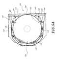
- FIG. 5Ais a cross-sectional top view of the wafer support storage FOUP of FIG. 4, taken along lines 5 — 5 of FIG. 4, shown with the FOUP door closed and a wafer support according to one preferred embodiment of the invention;
- FIG. 5Bis a cross-sectional top view of the wafer support storage FOUP of FIG. 4, taken along lines 5 — 5 of FIG. 4, shown with the FOUP door closed and a wafer support according to another preferred embodiment of the invention;
- FIG. 6Ais a cross-sectional top view of the wafer support storage FOUP of FIG. 4, taken along lines 6 — 6 of FIG. 4, showing the transfer station holding the wafer support of FIG. 5A;
- FIG. 6Bis a cross-sectional top view of the wafer support storage FOUP of FIG. 4, taken along lines 6 — 6 of FIG. 4, showing the transfer station holding the wafer support of FIG. 5B;
- FIG. 7is a cross section of an exemplary edge support end effector for use with preferred embodiments of the invention.
- FIG. 8is a top view of an exemplary contact end effector for use with preferred embodiments of the invention.
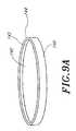
- FIG. 9Ais a perspective view of a wafer supported on a wafer support in accordance with preferred embodiments of the invention.
- FIG. 9Bis a cross-sectional view of the wafer and wafer support of FIG. 9A;
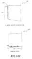
- FIG. 10Ais a schematic illustration showing an exemplary configuration for a FOUP in accordance with preferred embodiments of the invention.
- FIG. 10Bis a schematic illustration showing another exemplary configuration for a FOUP in accordance with preferred embodiments of the invention.
- FIG. 10Cis a schematic illustration showing yet another exemplary configuration for a FOUP in accordance with preferred embodiments of the invention.
- wafer supportsare provided for supporting a wafer during a semiconductor fabrication process.
- the wafer supportscan be removably stored in the storage accommodations of a wafer support holder.
- the wafer support holderis similar to a standard wafer boat used for semiconductor processing and holds the wafers and wafer supports during processing in a furnace.
- the wafer supportscan also be removably stored in the storage accommodations of a wafer processing cassette, such as a front opening unified pod (FOUP), that has been adapted to accommodate the wafer supports that are of slightly different dimensions than the wafers.
- FOUPfront opening unified pod
- the wafer supportspreferably support a wafer, over an entire perimeter of a wafer, in which case the wafer supports desirably have increased hoop strength in comparison to supports which do not extend around the entire perimeter of the wafer. More preferably, the wafer supports support a substantial portion of a wafer.
- the supportcan comprise a plate of material, which can support the entire bottom surface of a wafer. In other embodiments, the wafer support can be in the shape of a ring. In supporting a “substantial portion” of a wafer, the wafer support extends under the wafer to cover greater than about 10%, preferably greater than about 50% and more preferably greater than about 90% of the bottom surface of the wafer.
- a transfer or loading stationfor placing a wafer on a wafer support and for removing a wafer from a wafer support.
- the transfer stationcomprises an accommodation for a wafer support at a first level and an accommodation for a wafer at a second level, the second level being above the first level.
- FIG. 1A flow diagram of an exemplary procedure for loading and processing a batch of wafers in accordance with preferred embodiments of the invention is given schematically in FIG. 1 .
- a wafer supportis transported to a transfer station from a wafer support storage position. This transfer can be performed using a robot end effector designed for wafer transport. The robot end effector contacts the wafer support from the bottom and transports the wafer support to the transfer station. At the transfer station, the robot places the wafer support at a first level.
- a waferis also transported to the transfer station.
- the waferoccupies a second level in the transfer station, above the first level.
- the waferWhile still in the transfer station, the wafer is then seated upon the wafer support, as indicated by 14 . Then the wafer, together with the wafer support upon which it is seated, is transported to the wafer support holder or “boat” as indicated by 16 .
- the systemchecks if loading of the batch of wafers has been completed. It will be appreciated that the system includes a processor and memory programmed to conduct the indicated steps by controlling the robot and other system mechanisms. If loading has not been completed, the previous sequence is repeated, as indicated by loop 24 .
- the wafersare preferably loaded into the wafer support holder sequentially, such as from the topmost slot down to the bottommost slot.
- the wafer support holderis loaded into a process chamber, such as a furnace, as indicated by 20 .
- loading the wafer/support combinationscan be conducted through a door while the wafer support holder is positioned within the process chamber.
- processingcan be performed at very high temperatures, preferably greater than about 1000° C., more preferably greater than about 1200° C. and most preferably greater than about 1300° C.
- the wafersare unloaded (not shown) in reverse order.
- the robot end effectorcan be an edge support end effector, contacting both the wafer support and the wafer at its edges, or it can be a more conventional end effector, contacting both the wafer support and the wafer towards the center of its bottom surface, or it can be a combination of these two end effectors, e.g. an end effector that contacts the wafer support at its edges and contacts the wafer towards the center of its bottom surface.
- the end effectorcan be any end effector suitable for holding the wafer support and the wafer and for performing the actions described herein.
- edge support end effectorsare particularly suitable for ring shaped wafer supports, while wafer supports which are plates may be held with end effectors contacting the wafer supports at the edges or more central regions on the bottom surface of the wafer supports.
- Exemplary end effectorsare disclosed in U.S. Provisional Application No. 60/377,904, filed May 2, 2002, and corresponding U.S. application Ser. No. 10/361,480 entitled TWO LEVEL END EFFECTOR, filed Feb. 5, 2003 by den Hartog, the disclosures of which are incorporated herein by reference.
- the wafer supports supporting the waferpreferably comprise a circular plate, i.e., a structure that supports the entire bottom surface area of a wafer seated upon it (see FIGS. 5A and 6A and corresponding text below).
- the wafer supportcan also be in the shape of a ring, i.e. a structure with a vacant center (see FIGS. 5B and 6B and corresponding text below). It will be appreciated that while the support “ring” can have a circular shape, the support “ring” need not be round, it may be, e.g. in a hexagonal, or even square, shape so long as associated apparatus are configured to accept that shape.
- the wafer supportscan permanently reside in the processing system.
- theycan be stored in the wafer support holder before and after processing.
- the wafer supportsare stored in and supplied to a processing system in a cassette, and more particularly in a FOUP adapted to accommodate the wafer supports.
- This adaptationrequires only that the support frame for holding the wafer supports inside the FOUP be changed from the FOUP's standard construction. As such, the outer surfaces of the FOUP can retain their standard construction.
- the wafer supportsare configured to support a 300 mm wafer and, so, have a diameter that is slightly larger than the diameter of a 300 mm wafer.
- the transfer stationis provided as part of the FOUP holding the wafer supports.
- These adapted FOUPscan interface with the processing system via commercially available FOUP-receiving stations, which comprise a FOUP door opener.
- FOUP-receiving stationswhich comprise a FOUP door opener.
- this embodimentis particularly well adapted for retrofitting existing systems.
- the transfer stationcan be located at any point between the upper and lower ends of the FOUP, or at either of the upper or lower ends.
- the transfer stationis located at the lower end of the FOUP.
- the wafersare preferably also supplied to a processing system in cassettes.
- a standard FOUPpreferably serves as the cassette used to provide wafers to the processing system.
- the FOUPinterfaces with a FOUP station, comprising a FOUP door opener, provided in the processing system.
- a FOUP storing wafer supportsmay contain a transfer station
- the FOUP storing wafersmay also contain a transfer station.
- the transfer stationcan exist in a structure independent of either the FOUPs storing the wafers or the wafer supports.
- wafer and wafer support accommodations in the transfer stationcan comprise various types of support structures used for loading and unloading wafers onto wafer supports.
- placing a wafer on a wafer supportcan be done in several ways.
- the support structures for the wafer supportcan be moveable in a vertical direction while the wafer remains stationary.
- the support structures for the wafercan be moveable in a vertical direction while the wafer support remains stationary.
- both the support structures for the wafer and the support structure for the wafer supportare moveable.
- the support structures for the wafercan move such that the wafer is moved towards the wafer support (or vice versa or both the wafer and the wafer support can move) until the wafer rests on the wafer support.
- a wafer supportis preferably provided with cut-aways (e.g., through holes) to allow for vertical movement of those support structures and of the wafer independent of the wafer support itself.
- all the support structures in the transfer stationare stationary. Vertical movement to place the wafer on the wafer support is carried out by a robot that transports the wafer support upwardly to contact the wafer. Accordingly, the preferred embodiments advantageously allow wafers to be provided to a process chamber on wafer supports that support a substantial portion of a wafer's bottom surface area, including the entire perimeter of a wafer.
- FIGS. 2 and 3an exemplary wafer processing system containing a process chamber is illustrated and indicated generally by the reference numeral 30 .
- the exemplary system 30 of FIGS. 2 and 3comprises a housing 32 and is generally installed in a so-called “clean room.”
- partitions 33 , 34 and 35are also present.
- the housing 32delimits, with the partition 33 , a processing chamber 51 .
- the processing area 51comprises reactors, which in this example, are vertical furnaces 36 , 37 .
- the housing 32 and the partitions 33 and 34define a wafer handling section or chamber 52 .
- a cassette transfer section or chamber 53is defined between the housing 32 and partitions 34 and 35 .
- An input/output station, to transfer cassettes into and out of the system 30is indicated by reference numeral 63 .
- Wafersare supplied in cassettes 40 , which are placed on the input/output station 63 .
- a FOUPaccording the preferred embodiments preferably serves as the cassette 40 .
- a cassette handling device 61transfers the cassettes 40 from the input/output station 63 through a closable opening 64 into a cassette store 38 located in the cassette transfer section 53 .
- the cassette store 38is provided with a number of vertically aligned rotary platforms 57 on which the cassettes 40 are stored.
- the cassette handling device 61is movable in a vertical direction by means of an elevator 65 so that the different platforms 57 can be reached.
- the cassette handling device 61is provided with a cassette end effector 62 , which has dimensions a little smaller than those of a series of cut-outs 56 in the rotary platforms 57 .
- the end effector 62 of the cassette handling device 61can be lowered through one of the cut-outs 56 in one of the platforms 57 to place the cassette 40 on the platform 57 .
- the cassette handler 61can be retracted from the cassette store 38 .
- the cassette handling device 61is mounted such that it is able to transfer cassettes 40 between the input/output station 63 and the store 38 .
- the device 61is also capable of transferring cassettes 40 between the store 38 and a rotatable cassette transfer platform 60 , or between the input/output station 63 and the rotatable cassette transfer platform 60 .
- the rotatable cassette transfer platform 60is constructed such that, on rotation, the cassette 40 is placed against the partition 34 between the cassette transfer section 53 and the wafer handling section 52 .
- the partition 34is provided with a closure and a closure mechanism, together forming an interface schematically indicated by the reference numeral 67 . After placing the cassette against the interface 67 in the partition 34 , the closure mechanism grips and unlocks the closure of the cassette and simultaneously opens the closure in the partition 34 and the closure of the cassette.
- a wafer handling device 54 within the wafer handling section 52transfers wafers between the cassette concerned and a wafer support holder 42 .
- the wafer support holder 42accommodates more wafers than can be held in the cassettes of the preferred embodiments, i.e., more than 25 wafers when using presently standard FOUPs, preferably more than 50 wafers and more preferably greater than 70 wafers.
- the wafer handling device 54preferably comprises a robot end effector 59 configured to handle individual wafers.
- the wafer handling device 54To load a wafer into the wafer support holder 42 , the wafer handling device 54 first transfers a wafer from a cassette 40 to a transfer station, e.g., contained within the cassette 40 , and then transfers a wafer support from a storage position, e.g., contained in the wafer support holder 42 , to the transfer station. After seating the wafer upon the wafer support, the wafer, situated on the wafer support, is loaded into the wafer support holder 42 .
- Each of the wafer support holders 42preferably comprises a wafer boat or rack supported on a pedestal.
- a doorplateis preferably provided below each of the pedestals.
- both the wafers and the wafer supportsare preferably provided to the processing system 30 in FOUPs, with a closure in the interface 67 for each FOUP (not shown).
- two rotatable cassette platforms 60orient both FOUPs so that they are simultaneously open to the wafer handling section 52 .
- a transfer arm 46preferably moves the wafer support holder 42 upon a support surface 47 through an openable closure 49 in the partition 33 from the wafer handling chamber 52 into the processing chamber 51 .
- the illustrated processing section 51is provided with a rotary transfer platform 41 , supporting a plurality of wafer support holders 42 .
- Two reactors, which in this case comprise furnaces 36 , 37are arranged in the processing chamber 51 .
- the furnaces 36 , 37are positioned vertically and wafer support holders 42 , filled with wafer/wafer support combinations 43 , are introduced vertically into the furnaces 36 , 37 from below.
- each furnace 36 , 37has an insertion arm 44 , which is movable in the vertical direction.
- the doorplates below the wafer support holders 42serve to seal the reactors from the outside processing section when the wafer support holders 42 are lifted up into the reactors.
- the processing of a large number of waferscan be carried out as follows: the operator, shown diagrammatically in FIG. 2, loads the store 38 by introducing a number of cassettes 40 on the input/output station 63 and carrying out control operations on a control panel 66 .
- Each of the cassettes 40is transferred from the input/output station 63 with the aid of the cassette handling device 61 into the storage compartments 39 made for these cassettes in the store 38 , specifically on the stacked rotary platforms 57 .
- By rotation of the store 38 and use of the elevator 65it is possible to fill various compartments with the cassettes 40 . After filling the store 38 , no further human interaction is required with this exemplary automated installation.
- the cassettes 40 concernedare then removed from the store 38 by the cassette handler device 61 and placed on the cassette transfer platform 60 .
- the cassette transfer platform 60comprises two levels, schematically indicated in FIG. 2, each level capable of receiving a cassette, where the two levels can be rotated independently of one another. Upon rotation of the cassette transfer platform 60 , the cassettes are placed against the partition 34 .
- a transfer stationis located in a FOUP providing either wafers or wafer supports to the process chamber 51
- one platform 60can accommodate FOUPs for providing wafers while the other platform accommodates FOUPs for providing wafer supports.
- the FOUPs on both levelsmay then be simultaneously open to the handling chamber 52 .
- the wafersare removed by the wafer handler 54 , transported to the transfer station, seated upon a wafer support and the wafer/support combination 43 is placed in a wafer support holder 42 .
- the closure 49 in partition 33is opened and the wafer boat or support holder 42 is placed on the transfer platform 41 by the transfer arm 46 .
- the transfer platform 41then moves the wafer support holder 42 within the process chamber 51 to a position below the reactor to be loaded.
- the insertion mechanism or elevator 44moves the wafer support holder 42 into the reactor 36 or 37 .
- Treated wafersmove counter to the course described above after being lowered and cooled within the process chamber 51 .
- a FOUPaccording to a preferred embodiment of the invention is indicated in its entirety by reference numeral 100 .
- the FOUP 100comprises a housing 102 , which is provided at one end with a flange 104 to receive a door 110 (FIGS. 5 A and 5 B).
- a mechanical interface 106is preferably provided for supporting the FOUP 100 on a support table.
- the outer surfaces of the FOUP 100including the housing 102 and the bottom interface 106 , are configured in accordance with SEMI standards.
- a support structure 120is provided inside the housing 102 .
- the support structure 120is mounted at the lower side of the housing with bolts 122 .
- Attached to the support structure 120are vertically extending support beams 130 and 136 , provided with surfaces 132 and 138 to hold the wafer supports 140 .
- Each surface 132is provided with a support ridge 134 with sloped sides.
- the support ridge 134fits into a hole 142 in the wafer support 140 to provide centering and positioning capabilities for the wafer supports 140 .
- the surfaces 132 and 138 , the support ridge 134 and the volume inside the FOUP 100 for accommodating a wafer support 140together comprise a storage accommodation 141 .
- 23 storage accommodations 141 for wafer supports 140are illustrated, of which a bottom accommodation 141 is shown empty.
- an unadapted form of the illustrated FOUP 100can accommodate 25 wafers 160 .
- a transfer station 143is preferably provided instead.
- the transfer station 143preferably comprises three pins 150 , each pin provided with a conical lower end 152 on which a wafer support 140 can be supported and a cylindrical upper part 153 , on top of which a wafer 160 can be supported.
- the material of the pins 150is PEEKTM (poly-ether-ether-ketone) or another material that is not damaging to wafers, such as TeflonTM or polypropylene.
- each wafer support 140is preferably provided with three holes 142 .
- the wafer support 140In order to place a wafer 160 onto a wafer support 140 , the wafer support 140 is transferred to the transfer station 143 from its storage accommodation 141 in the FOUP 100 .
- the storage accommodations 141have enough height such that a robot end effector 154 can move between adjacent wafer supports 140 without unintentional touching of those supports 140 .
- a robot end effector 154contacts the wafer support 140 from its bottom, taking the wafer support 140 off the surfaces 132 and 138 and off the support ridge 134 .
- the wafer support 140While on the end effector 154 , the wafer support 140 is then moved by a robot from its storage accommodation 141 to the transfer station 143 , provided at the lower end of the FOUP 100 .
- the robotplaces the wafer support 140 so that its holes 142 pass over the cylindrical upper parts 153 of the support pins and the wafer support rests on the conical part 152 of the support pins 150 .
- the position of the wafer supports 140can be locked in the storage accommodations 141 by the support ridges 134 .
- this lockingensures that the wafer supports 140 are correctly oriented for transport to the transfer station 143 , such that the position of the holes 142 in the wafer supports 140 align with the positions of the pins 150 when the wafer supports 140 are moved to the transfer station 143 .
- a wafer 160is also transferred to the transfer station 143 and is placed on top of the pins 150 .
- the upper end of pins 150is high enough so that there is enough space for the end effector 154 to lower out of contact with the wafer 160 , then retract and move between the lower surface of a wafer 160 supported on pins 150 and an upper surface of a wafer support 140 supported on the conical part 152 of pins 150 without unintentional touching of the wafer 160 or the wafer support 140 .
- the robotretracts the end effector 154 , moves it vertically to a level below the lower surface of wafer support 140 and then extends it again, so that the end effector 154 is now placed below the wafer support 140 , which, as discussed above, has been positioned on the conical part 152 of the pins 150 .
- the end effector 154next moves upward. In doing so the end effector 154 contacts and lifts the wafer support 140 , causing the wafer support 140 to contact and lift the wafer 160 .
- both the wafer support 140 and the wafer 160are lifted above the pins 150 , with the wafer 160 resting upon the wafer support 140 .
- the robotcan transport the wafer support 140 together with the wafer 160 to the boat or wafer support holder 42 (FIG. 2 ), where the wafers 160 are subjected to a semiconductor fabrication process.
- FIGS. 5A and 5Billustrate cross-sectional top views of the FOUP 100 with door 110 of the FOUP 100 shown in a closed position in each Figure.
- the wafer support 140is a circular plate and in FIG. 5B the wafer support 140 is a ring having a circular shape and an inner circumference or boundary 146 .
- the wafer support 140is locked in its stored orientation by the support ridge 134 , at the side opposite the door 110 .
- the wafer support 140preferably has a raised edge 144 that can shield the edge of a wafer 160 (FIG. 9) against excessive heat radiation during processing.
- FIGS. 6A and 6Billustrate cross-sectional top views of the transfer station 143 in the FOUP 100 , with the wafer support 140 in FIG. 6A being a circular plate and the wafer support 140 in FIG. 6B being a circular ring.
- the end effector 154can contact the wafer support 140 and/or a wafer 160 (not shown) at its bottom surface, typically at its center.
- Such an exemplary end effectoris described in U.S. Provisional Application No. 60/377,904, filed May 2, 2002, and corresponding U.S. Application No. 10/361,480 entitled TWO LEVEL END EFFECTOR, filed Feb. 5, 2003 by den Hartog, the disclosures of which are incorporated herein by reference.
- FIG. 60/377,904filed May 2, 2002
- U.S. Application No. 10/361,480 entitled TWO LEVEL END EFFECTORfiled Feb. 5, 2003 by den Hartog, the disclosures of which are incorporated herein by reference.
- the end effector 154extends across the diameter of the ring to contact opposite sides of the wafer support 140 and/or wafer 160 (not shown) and can be, e.g., an edge support end effector (see FIGS. 6 B and 7 ).
- an edge support end effectoris also described in U.S. Provisional Application No. 60/377,904 and U.S. Utility Application No. 10/361,480, entitled TWO LEVEL END EFFECTOR, filed Feb. 5, 2003 by den Hartog. It will be appreciated that edge support end effectors are suitable for use with the wafer support 140 whether the wafer support 140 is a plate or a ring.
- the wafer support 140rests on the pins 150 and the end effector 154 is present below the wafer support 140 .
- a mechanical side interface of the FOUP 100is indicated with reference numeral 108 .
- the wafer support 140is preferably displaced outwardly relative to wafer supports 140 housed in the storage accommodations 141 . In this way, the wafer support 140 is sufficiently clear from the support beams 136 such that the wafer support 140 can be vertically moved to an extent sufficient for loading and unloading of the wafer support 140 and the wafer 160 .
- FIG. 7A particularly simple edge support end effector for transporting wafer supports and/or wafers is illustrated in FIG. 7 .
- the illustrated end effector 154is provided with sloped contact surfaces 167 that contact and support wafer support 140 or a wafer (not shown) at their edges.
- an end effector 154can be used that contacts the wafer 160 at its bottom surface, typically in a central region of the wafer 160 .
- the length of the end effector 154is preferably long enough such that an annular wafer support 140 is supported at two opposing parts of the ring.
- An example of such an end effectoris shown in FIG. 8 .
- the contact surface supporting the wafer 160is indicated by reference numeral 166 and the contact surface supporting the annular wafer support is indicated by reference numeral 168 .
- the contacting surfaces 168have a large enough radius to accommodate wafer 160 (not shown) without contacting the wafer 160 while the wafer 160 is supported upon the surface 166 .
- FIGS. 9A and 9Bshow, in isolation, perspective and cross-sectional views, respectively, of the wafer 160 supported on the wafer support 140 in one preferred embodiment of the invention.
- the wafer support 140preferably has a raised shoulder or edge 144 that can shield the edge 145 of a wafer 160 against receiving excessive heat radiation during heat up, preventing overheating of the edge 145 .
- the raised edge 144advantageously minimizes horizontal movement of the wafer 160 during transport of the wafer support 140 with the wafer 160 thereon.
- the transfer station 143is preferably provided at the lower end of a FOUP, in other embodiments it can be placed at an upper end of the FOUP or at a selected point between the upper and lower ends of the FOUP. In yet other embodiments, the transfer station 143 can be placed at another position in the treatment system, e.g., at a fixed position and not in a FOUP.
- FIGS. 10A-10Cillustrate schematically the above-described configuration for the FOUP 100 , along with two exemplary alternative configurations.
- FIG. 10Aillustrates the configuration described above with respect to FIGS. 4-6.
- Reference numeral 601indicates all storage accommodations 141 for wafer supports and/or wafers in the FOUP 100 .
- a total of 23 stripes 603are indicated, the space directly above each stripe 603 representing one of 23 storage accommodations 141 .
- Reference numeral 143indicates the transfer station.
- the two lines 602indicate the space above support pins 150 that is required for robotic transfer of wafer support 140 and wafer 160 .
- the pins 150 of the transfer station 143 at the bottom of the FOUP 100are shifted slightly outwardly, so that the transfer station 143 can be shifted downwardly along the lower wall 604 while still being able to accommodate wafer supports 140 and wafers 160 on the pins 150 (FIGS. 6 A and 6 B).
- the pins 150 in this configurationare shifted outwardly in the direction of the opening 606 of the FOUP 100 .
- a wafer support 160 resting on the pins 150 at the transfer station 143sticks out of the FOUP 100 (FIG. 4 ).
- the number of wafer support accommodations 141is reduced to 21, with the space directly above each stripe 603 representing one of the 21 storage accommodations 141 .
- the transfer station 143can be shifted inward relative to the arrangement illustrated in FIG. 10A and, so, can be positioned coaxially aligned with the storage accommodations 141 .
- the door (not shown) of the FOUP 100can be closed.
- FIG. 10Cthe storage function and the transfer function are completely separated.
- Storage accommodations 141are contained in one FOUP 100 , while the transfer station 143 is formed in a separate station 100 ′ completely separate from the FOUP 100 .
- the total number of storage accommodations 141 that fit into the interior space of a FOUP containing a transfer station 143is only limited by available space and the ancillary transfer station equipment. In the configurations illustrated in FIGS. 10A-10C, this number can range from 0 (the configuration station 100 ′ of FIG. 10C) to about 23 (the configuration of FOUP 100 of FIG. 10 A).
- the FOUPcan fit more or fewer storage accommodations 141 , however, if the interior space of the FOUP is increased or decreased, e.g., if the height of the FOUP is increased or decreased.
- the illustrated FOUPsprovide a particular number of accommodations 141 for wafer supports 140
- the total number of wafers 160 and wafer supports 140 to be loaded in a cassette formed in accordance with the teachings hereinare not limited by the present teachings and can be varied.
- the number of wafers 160 and wafer supports 140can be 25 or 50 or any number that can be accommodated by the processing system.
- the wafer supports 140can be provided in more than one FOUP, if necessary.
- holes 142are illustrated as both allowing support pins 150 to pass through them to support the wafer 160 in the transfer station 143 and to lock the wafer supports 140 upon the surfaces 132 (typically by way of the support ridges 134 ) in the storage accommodations 141 , separate holes and/or grooves can be provided for each of these functions, at each of these locations.
- different sets of support structures in the transfer station 143can be used to support the wafer support 140 and the wafer 160 , respectively.
- the pins 150can be used to solely support the wafer 160
- the wafer support 140can be supported by other support structures, e.g., a set of pins separate from the pins 150 .
- the wafer support 140can be supported on its lower surface and the wafer 160 can be supported on elevated structures, such as pins, in the central, open area of an annular wafer support 140 (see, e.g., FIG. 6 B), so long as the movement of the end effector 154 is not obstructed. In such a case, the wafer supports 140 need not be provided with holes 142 .
- the wafer supports 140are formed of quartz.
- the wafer supports 140are preferably formed of a material with high temperature resistance and that is available in high purity.
- Silicon carbide (SiC)is an example of such a material.
- the preferred SiC material for the wafer supportsis so-called “free-standing” CVD SiC. This is a SiC coating, initially deposited on a support material but with a thickness that is sufficient to allow removal of the support material.
- the support materialcan be, e.g., graphite.
- An exemplary method of forming a structure with “free-standing” CVD SiCis disclosed in U.S. Pat. No. 4,978,567, issued Dec. 18, 1990 to Miller, the disclosure of which is incorporated herein by reference.
- the wafers 160 and the wafer supports 140can be stored in cassettes, such as the FOUP 100 , that can be used with a standard furnace.
- a standard furnaceprovided with a standard wafer-handling robot, can easily be adapted for processing in conjunction with these preferred embodiments, without the need for significant changes in hardware.
- providing the wafer supports 140 in a special FOUP 100which simultaneously houses the transfer station 143 , is particularly efficient as it minimizes the movements of the wafer supports 140 during loading and unloading.
- the use of the FOUP 100 for storage and transport of the wafer supports 140allows easy access to other equipment provided with FOUP interfaces, such as cleaning equipment.
- wafer supports 140removable, to be placed in a standard design, slotted cassette, keeps the wafer supports 140 simple in shape and easy to manufacture.
Landscapes
- Engineering & Computer Science (AREA)
- Physics & Mathematics (AREA)
- Condensed Matter Physics & Semiconductors (AREA)
- General Physics & Mathematics (AREA)
- Manufacturing & Machinery (AREA)
- Computer Hardware Design (AREA)
- Microelectronics & Electronic Packaging (AREA)
- Power Engineering (AREA)
- Robotics (AREA)
- Container, Conveyance, Adherence, Positioning, Of Wafer (AREA)
Abstract
Description
This application claims the priority benefit of U.S. Provisional Application Ser. No. 60/365,122, filed Mar. 15, 2002, and U.S. Provisional Application Ser. No. 60/379,885, filed May 10, 2002.
This invention relates generally to semiconductor fabrication and, more particularly, to a method and apparatus for transferring and supporting wafers for batch processing in a furnace.
Heat-related complications can preclude the use of common wafer boats for very high temperature treatment or processing of a batch of wafers in a furnace, e.g., processing at temperatures up to about 1350° C. For example, common wafer boats may support wafers only at their edges. With such a support scheme, because the mechanical strength of a wafer can be reduced at very high temperatures, the wafer's own weight can cause it to plastically deform at very high temperatures.
Other available wafer boat wafer supports are described in U.S. Pat. Nos. 5,865,321 and 5,820,367. U.S. Pat. No. 5,865,321 describes a wafer boat having a wafer support with multiple inwardly extending arms to support the wafer at more inward locations. U.S. Pat. No. 5,820,367 describes a wafer boat that supports a wafer at a central location using the entire circumference of a ring support. The supports in these wafer boats, however, are still not sufficiently supportive to prevent plastic deformation and consequent crystallographic slip of the wafer. In order to prevent slip, wafers should be supported over a substantial portion of their bottom surface areas.
Wafer supports meeting this criteria are known for single wafer systems. For such systems, susceptors supporting wafers over their entire bottom surface area and support rings forming a complete circle to support a wafer at its perimeter are known in the prior art. Special measures, however, are required to place a wafer onto or to separate a wafer from such susceptors.
In particular, with such a single wafer system, when using a robot end effector according to the prior art, access to the wafer is generally provided from the bottom and the susceptor stays in place within a process chamber while wafers are serially loaded and unloaded. Typically, the robot end effector places a wafer on moveable pins at a level above the susceptor, the wafer being spaced sufficiently above the susceptor to allow enough clearance for retracting the robot end effector without the robot end effector touching the wafer or the susceptor. After retraction, the pins move downward to lower the wafer onto the susceptor. To unload the wafer, the reverse of these steps occurs. While suitable for single wafer processing, such a wafer loading and support system is not easily applicable to a batch processing system because, if possible at all, such a system would be unacceptably complicated and cumbersome, since it would require, inter alia, that every processing position be provided with moveable pins and the attendant hardware and control systems to move these pins.
Accordingly, it is an object of the present invention to provide a wafer boat with a wafer support system that, inter alia, provides support for wafers over a substantial portion of their bottom surface areas and that allows for efficient loading and unloading of the wafers for processing in a process chamber.
In accordance with one preferred embodiment of the invention, a method for semiconductor processing is provided. The method includes loading a wafer onto a wafer support in a transfer station, transporting the wafer into a process chamber from the transfer station and subjecting the wafer to a semiconductor fabrication process in the process chamber. During both transporting the wafer into the process chamber and subjecting the wafer to a semiconductor fabrication process, the wafer is seated upon the wafer support.
In accordance with another preferred embodiment, a method for handling a wafer and a wafer support for processing is provided. The method includes placing a wafer on a wafer support, subsequently transporting the wafer while seated upon the wafer support into a wafer boat, and subjecting the wafer to a semiconductor fabrication process while the wafer is seated upon the wafer support in the wafer boat.
In accordance with yet another preferred embodiment, a system for processing a substrate is provided. The system includes a plurality of substrate supports for supporting a plurality of substrates. The substrate supports support an entire perimeter of a substrate and are held in a substrate support holder, from which they can also be removed. A process chamber accommodates the substrate support holder during substrate processing. The system also comprises a substrate loading station that is configured to load a substrate onto a substrate support, where the substrate loading station is separate from the substrate support holder.
In accordance with another preferred embodiment, a semiconductor wafer cassette is provided. The cassette houses a wafer loading station that is configured for loading a wafer onto a wafer support.
The invention will be better understood from the detailed description of the preferred embodiments and from the appended drawings, which are meant to illustrate and not to limit the invention, and wherein:
FIG. 1 is a flow diagram illustrating processing of a batch of wafers in accordance with preferred embodiments of the invention;
FIG. 2 is a perspective view of an exemplary wafer processing system for use with preferred embodiments of the invention;
FIG. 3 is a schematic plan view of the system of FIG. 2;
FIG. 4 is a cross-sectional side view of a wafer support storage front opening unified pod (FOUP) comprising a transfer station and constructed in accordance with preferred embodiments of the invention;
FIG. 5A is a cross-sectional top view of the wafer support storage FOUP of FIG. 4, taken alonglines 5—5 of FIG. 4, shown with the FOUP door closed and a wafer support according to one preferred embodiment of the invention;
FIG. 5B is a cross-sectional top view of the wafer support storage FOUP of FIG. 4, taken alonglines 5—5 of FIG. 4, shown with the FOUP door closed and a wafer support according to another preferred embodiment of the invention;
FIG. 6A is a cross-sectional top view of the wafer support storage FOUP of FIG. 4, taken along lines6—6 of FIG. 4, showing the transfer station holding the wafer support of FIG. 5A;
FIG. 6B is a cross-sectional top view of the wafer support storage FOUP of FIG. 4, taken along lines6—6 of FIG. 4, showing the transfer station holding the wafer support of FIG. 5B;
FIG. 7 is a cross section of an exemplary edge support end effector for use with preferred embodiments of the invention;
FIG. 8 is a top view of an exemplary contact end effector for use with preferred embodiments of the invention;
FIG. 9A is a perspective view of a wafer supported on a wafer support in accordance with preferred embodiments of the invention;
FIG. 9B is a cross-sectional view of the wafer and wafer support of FIG. 9A;
FIG. 10A is a schematic illustration showing an exemplary configuration for a FOUP in accordance with preferred embodiments of the invention;
FIG. 10B is a schematic illustration showing another exemplary configuration for a FOUP in accordance with preferred embodiments of the invention; and
FIG. 10C is a schematic illustration showing yet another exemplary configuration for a FOUP in accordance with preferred embodiments of the invention.
According to preferred embodiments of the invention, wafer supports are provided for supporting a wafer during a semiconductor fabrication process. The wafer supports can be removably stored in the storage accommodations of a wafer support holder. The wafer support holder is similar to a standard wafer boat used for semiconductor processing and holds the wafers and wafer supports during processing in a furnace. The wafer supports can also be removably stored in the storage accommodations of a wafer processing cassette, such as a front opening unified pod (FOUP), that has been adapted to accommodate the wafer supports that are of slightly different dimensions than the wafers. The wafer supports preferably support a wafer, over an entire perimeter of a wafer, in which case the wafer supports desirably have increased hoop strength in comparison to supports which do not extend around the entire perimeter of the wafer. More preferably, the wafer supports support a substantial portion of a wafer. In one embodiment, the support can comprise a plate of material, which can support the entire bottom surface of a wafer. In other embodiments, the wafer support can be in the shape of a ring. In supporting a “substantial portion” of a wafer, the wafer support extends under the wafer to cover greater than about 10%, preferably greater than about 50% and more preferably greater than about 90% of the bottom surface of the wafer.
In addition to wafer supports, according to preferred embodiments of the invention, a transfer or loading station is also provided for placing a wafer on a wafer support and for removing a wafer from a wafer support. The transfer station comprises an accommodation for a wafer support at a first level and an accommodation for a wafer at a second level, the second level being above the first level. During loading, the wafer and wafer support, initially at the second and first levels, respectively, are made to contact. In contacting, the wafer is seated upon the wafer support. During unloading, the wafer and wafer support, initially at the same level, are made to separate, coming to rest at the second and first levels, respectively.
A flow diagram of an exemplary procedure for loading and processing a batch of wafers in accordance with preferred embodiments of the invention is given schematically in FIG.1. As indicated by10, a wafer support is transported to a transfer station from a wafer support storage position. This transfer can be performed using a robot end effector designed for wafer transport. The robot end effector contacts the wafer support from the bottom and transports the wafer support to the transfer station. At the transfer station, the robot places the wafer support at a first level.
As indicated by12, a wafer is also transported to the transfer station. The wafer occupies a second level in the transfer station, above the first level.
While still in the transfer station, the wafer is then seated upon the wafer support, as indicated by14. Then the wafer, together with the wafer support upon which it is seated, is transported to the wafer support holder or “boat” as indicated by16.
In the step indicated by18, the system checks if loading of the batch of wafers has been completed. It will be appreciated that the system includes a processor and memory programmed to conduct the indicated steps by controlling the robot and other system mechanisms. If loading has not been completed, the previous sequence is repeated, as indicated byloop 24. The wafers are preferably loaded into the wafer support holder sequentially, such as from the topmost slot down to the bottommost slot. When loading is completed, e.g., preferably, when a full batch of wafers, supported on wafer supports, has been loaded into the wafer support holder, the wafer support holder is loaded into a process chamber, such as a furnace, as indicated by20. Alternatively, loading the wafer/support combinations can be conducted through a door while the wafer support holder is positioned within the process chamber.
In the process chamber the wafers are subjected to processing as indicated by22. Advantageously, processing can be performed at very high temperatures, preferably greater than about 1000° C., more preferably greater than about 1200° C. and most preferably greater than about 1300° C. After processing, the wafers are unloaded (not shown) in reverse order.
Preferably, transfer of the wafer supports and of the wafers into and out of the transfer station is performed using the same robot and the same end effector. It will be appreciated, however, that different robots and/or different end effectors can be used in other arrangements to move the wafer supports and wafers. In particular, depending upon the wafer support used, the robot end effector can be an edge support end effector, contacting both the wafer support and the wafer at its edges, or it can be a more conventional end effector, contacting both the wafer support and the wafer towards the center of its bottom surface, or it can be a combination of these two end effectors, e.g. an end effector that contacts the wafer support at its edges and contacts the wafer towards the center of its bottom surface. More generally, the end effector can be any end effector suitable for holding the wafer support and the wafer and for performing the actions described herein. For example, edge support end effectors are particularly suitable for ring shaped wafer supports, while wafer supports which are plates may be held with end effectors contacting the wafer supports at the edges or more central regions on the bottom surface of the wafer supports. Exemplary end effectors are disclosed in U.S. Provisional Application No. 60/377,904, filed May 2, 2002, and corresponding U.S. application Ser. No. 10/361,480 entitled TWO LEVEL END EFFECTOR, filed Feb. 5, 2003 by den Hartog, the disclosures of which are incorporated herein by reference.
The wafer supports supporting the wafer preferably comprise a circular plate, i.e., a structure that supports the entire bottom surface area of a wafer seated upon it (see FIGS. 5A and 6A and corresponding text below). The wafer support can also be in the shape of a ring, i.e. a structure with a vacant center (see FIGS. 5B and 6B and corresponding text below). It will be appreciated that while the support “ring” can have a circular shape, the support “ring” need not be round, it may be, e.g. in a hexagonal, or even square, shape so long as associated apparatus are configured to accept that shape.
In one embodiment, the wafer supports can permanently reside in the processing system. For example, they can be stored in the wafer support holder before and after processing. In another embodiment, the wafer supports are stored in and supplied to a processing system in a cassette, and more particularly in a FOUP adapted to accommodate the wafer supports. This adaptation requires only that the support frame for holding the wafer supports inside the FOUP be changed from the FOUP's standard construction. As such, the outer surfaces of the FOUP can retain their standard construction. Preferably, the wafer supports are configured to support a 300 mm wafer and, so, have a diameter that is slightly larger than the diameter of a 300 mm wafer.
In addition, in a preferred embodiment the transfer station is provided as part of the FOUP holding the wafer supports. These adapted FOUPs can interface with the processing system via commercially available FOUP-receiving stations, which comprise a FOUP door opener. As such, this embodiment is particularly well adapted for retrofitting existing systems. Moreover, the transfer station can be located at any point between the upper and lower ends of the FOUP, or at either of the upper or lower ends. Preferably, the transfer station is located at the lower end of the FOUP.
The wafers are preferably also supplied to a processing system in cassettes. For wafers with a diameter of 300 mm, a standard FOUP preferably serves as the cassette used to provide wafers to the processing system. The FOUP interfaces with a FOUP station, comprising a FOUP door opener, provided in the processing system. As such, in another embodiment, just as a FOUP storing wafer supports may contain a transfer station, the FOUP storing wafers may also contain a transfer station. Advantageously, when used in a processing system in which wafer supports permanently reside in the processing system, such a FOUP precludes the need for the processing system to be significantly retrofitted with, e.g., a separate transfer station. It will be appreciated that in yet other embodiments, the transfer station can exist in a structure independent of either the FOUPs storing the wafers or the wafer supports.
Inside the transfer station, wafer and wafer support accommodations in the transfer station can comprise various types of support structures used for loading and unloading wafers onto wafer supports. As such, placing a wafer on a wafer support can be done in several ways. For example, in one embodiment, the support structures for the wafer support can be moveable in a vertical direction while the wafer remains stationary. In another embodiment, the support structures for the wafer can be moveable in a vertical direction while the wafer support remains stationary. In yet another embodiment, both the support structures for the wafer and the support structure for the wafer support are moveable. For example, after placing a wafer support and a wafer in the storage accommodations, the support structures for the wafer can move such that the wafer is moved towards the wafer support (or vice versa or both the wafer and the wafer support can move) until the wafer rests on the wafer support. A wafer support is preferably provided with cut-aways (e.g., through holes) to allow for vertical movement of those support structures and of the wafer independent of the wafer support itself.
In another particularly simple embodiment, all the support structures in the transfer station are stationary. Vertical movement to place the wafer on the wafer support is carried out by a robot that transports the wafer support upwardly to contact the wafer. Accordingly, the preferred embodiments advantageously allow wafers to be provided to a process chamber on wafer supports that support a substantial portion of a wafer's bottom surface area, including the entire perimeter of a wafer.
Reference will now be made to the Figures, wherein like numerals refer to like parts throughout.
With reference to FIGS. 2 and 3, an exemplary wafer processing system containing a process chamber is illustrated and indicated generally by thereference numeral 30. Theexemplary system 30 of FIGS. 2 and 3 comprises ahousing 32 and is generally installed in a so-called “clean room.” In addition to thehousing 32,partitions 33,34 and35 (omitted from FIG. 2 for clarity of illustration) are also present. Thehousing 32 delimits, with thepartition 33, aprocessing chamber 51. Theprocessing area 51 comprises reactors, which in this example, arevertical furnaces housing 32 and thepartitions 33 and34 define a wafer handling section orchamber 52. A cassette transfer section orchamber 53 is defined between thehousing 32 andpartitions 34 and35. An input/output station, to transfer cassettes into and out of thesystem 30, is indicated byreference numeral 63.
Wafers are supplied incassettes 40, which are placed on the input/output station 63. A FOUP according the preferred embodiments preferably serves as thecassette 40. Acassette handling device 61 transfers thecassettes 40 from the input/output station 63 through a closable opening64 into acassette store 38 located in thecassette transfer section 53. Thecassette store 38 is provided with a number of vertically alignedrotary platforms 57 on which thecassettes 40 are stored. Thecassette handling device 61 is movable in a vertical direction by means of anelevator 65 so that thedifferent platforms 57 can be reached. Thecassette handling device 61 is provided with acassette end effector 62, which has dimensions a little smaller than those of a series of cut-outs 56 in therotary platforms 57. When thecassette handling device 61 has transferred acassette 40 into thestore 38, theend effector 62 of thecassette handling device 61 can be lowered through one of the cut-outs 56 in one of theplatforms 57 to place thecassette 40 on theplatform 57. Subsequently, thecassette handler 61 can be retracted from thecassette store 38. Thecassette handling device 61 is mounted such that it is able to transfercassettes 40 between the input/output station 63 and thestore 38. Thedevice 61 is also capable of transferringcassettes 40 between thestore 38 and a rotatablecassette transfer platform 60, or between the input/output station 63 and the rotatablecassette transfer platform 60.
The rotatablecassette transfer platform 60 is constructed such that, on rotation, thecassette 40 is placed against the partition34 between thecassette transfer section 53 and thewafer handling section 52. The partition34 is provided with a closure and a closure mechanism, together forming an interface schematically indicated by thereference numeral 67. After placing the cassette against theinterface 67 in the partition34, the closure mechanism grips and unlocks the closure of the cassette and simultaneously opens the closure in the partition34 and the closure of the cassette.
Awafer handling device 54 within thewafer handling section 52 transfers wafers between the cassette concerned and awafer support holder 42. Thewafer support holder 42 accommodates more wafers than can be held in the cassettes of the preferred embodiments, i.e., more than 25 wafers when using presently standard FOUPs, preferably more than 50 wafers and more preferably greater than 70 wafers. As discussed herein, thewafer handling device 54 preferably comprises a robot end effector59 configured to handle individual wafers. To load a wafer into thewafer support holder 42, thewafer handling device 54 first transfers a wafer from acassette 40 to a transfer station, e.g., contained within thecassette 40, and then transfers a wafer support from a storage position, e.g., contained in thewafer support holder 42, to the transfer station. After seating the wafer upon the wafer support, the wafer, situated on the wafer support, is loaded into thewafer support holder 42. Each of thewafer support holders 42 preferably comprises a wafer boat or rack supported on a pedestal. A doorplate is preferably provided below each of the pedestals.
It will be appreciated that where a transfer station is not contained within the FOUP orcassette 40 containing wafers, a separate transfer station (not shown) is provided in thewafer handling section 52. It will also be appreciated that, in another embodiment, both the wafers and the wafer supports are preferably provided to theprocessing system 30 in FOUPs, with a closure in theinterface 67 for each FOUP (not shown). In such an embodiment, tworotatable cassette platforms 60 orient both FOUPs so that they are simultaneously open to thewafer handling section 52.
After loading of wafers into thewafer support holder 42 is completed, atransfer arm 46 preferably moves thewafer support holder 42 upon asupport surface 47 through anopenable closure 49 in thepartition 33 from thewafer handling chamber 52 into theprocessing chamber 51. The illustratedprocessing section 51 is provided with arotary transfer platform 41, supporting a plurality ofwafer support holders 42. Two reactors, which in this case comprisefurnaces processing chamber 51. Thefurnaces wafer support holders 42, filled with wafer/wafer support combinations 43, are introduced vertically into thefurnaces furnace insertion arm 44, which is movable in the vertical direction. The doorplates below thewafer support holders 42 serve to seal the reactors from the outside processing section when thewafer support holders 42 are lifted up into the reactors.
The processing of a large number of wafers can be carried out as follows: the operator, shown diagrammatically in FIG. 2, loads thestore 38 by introducing a number ofcassettes 40 on the input/output station 63 and carrying out control operations on acontrol panel 66. Each of thecassettes 40 is transferred from the input/output station 63 with the aid of thecassette handling device 61 into the storage compartments39 made for these cassettes in thestore 38, specifically on thestacked rotary platforms 57. By rotation of thestore 38 and use of theelevator 65, it is possible to fill various compartments with thecassettes 40. After filling thestore 38, no further human interaction is required with this exemplary automated installation.
Thecassettes 40 concerned are then removed from thestore 38 by thecassette handler device 61 and placed on thecassette transfer platform 60. Thecassette transfer platform 60 comprises two levels, schematically indicated in FIG. 2, each level capable of receiving a cassette, where the two levels can be rotated independently of one another. Upon rotation of thecassette transfer platform 60, the cassettes are placed against the partition34. Advantageously, in embodiments where a transfer station is located in a FOUP providing either wafers or wafer supports to theprocess chamber 51, oneplatform 60 can accommodate FOUPs for providing wafers while the other platform accommodates FOUPs for providing wafer supports. The FOUPs on both levels may then be simultaneously open to the handlingchamber 52. In any case, after opening of the closure of the cassette, together with theclosure 67 in the partition34, the wafers are removed by thewafer handler 54, transported to the transfer station, seated upon a wafer support and the wafer/support combination 43 is placed in awafer support holder 42. After thewafer support holder 42 has been filled, and becomes available for one of thereactors closure 49 inpartition 33 is opened and the wafer boat orsupport holder 42 is placed on thetransfer platform 41 by thetransfer arm 46. Thetransfer platform 41 then moves thewafer support holder 42 within theprocess chamber 51 to a position below the reactor to be loaded. Then the insertion mechanism orelevator 44 moves thewafer support holder 42 into thereactor process chamber 51.
As described above, the wafer supports may be supplied to the processing system in cassettes, such as closable FOUPs. With reference now to FIG. 4, a FOUP according to a preferred embodiment of the invention is indicated in its entirety byreference numeral 100. TheFOUP 100 comprises ahousing 102, which is provided at one end with aflange 104 to receive a door110 (FIGS.5A and5B). At the bottom of theFOUP 100, amechanical interface 106 is preferably provided for supporting theFOUP 100 on a support table. Preferably, the outer surfaces of theFOUP 100, including thehousing 102 and thebottom interface 106, are configured in accordance with SEMI standards.
Inside thehousing 102, asupport structure 120 is provided. Thesupport structure 120 is mounted at the lower side of the housing withbolts 122.
Attached to thesupport structure 120 are vertically extendingsupport beams surfaces 132 and138 to hold the wafer supports140. Each surface132 is provided with asupport ridge 134 with sloped sides. Thesupport ridge 134 fits into ahole 142 in thewafer support 140 to provide centering and positioning capabilities for the wafer supports140. Thesurfaces 132 and138, thesupport ridge 134 and the volume inside theFOUP 100 for accommodating awafer support 140 together comprise astorage accommodation 141. In total, 23storage accommodations 141 for wafer supports140 are illustrated, of which abottom accommodation 141 is shown empty.
It will be appreciated that an unadapted form of the illustratedFOUP 100 can accommodate 25wafers 160. As illustrated, however, at the lower end of theFOUP 100, where twoadditional storage accommodations 141 are ordinarily found in cassettes designed for accommodating 25wafers 160, atransfer station 143 is preferably provided instead. Thetransfer station 143 preferably comprises threepins 150, each pin provided with a conicallower end 152 on which awafer support 140 can be supported and a cylindricalupper part 153, on top of which awafer 160 can be supported. Preferably, the material of thepins 150 is PEEK™ (poly-ether-ether-ketone) or another material that is not damaging to wafers, such as Teflon™ or polypropylene. To allow passage of the cylindricalupper parts 153 of thepins 150, eachwafer support 140 is preferably provided with threeholes 142.
In order to place awafer 160 onto awafer support 140, thewafer support 140 is transferred to thetransfer station 143 from itsstorage accommodation 141 in theFOUP 100. Thestorage accommodations 141 have enough height such that arobot end effector 154 can move between adjacent wafer supports140 without unintentional touching of thosesupports 140. To transfer awafer support 140, arobot end effector 154 contacts thewafer support 140 from its bottom, taking thewafer support 140 off thesurfaces 132 and138 and off thesupport ridge 134. While on theend effector 154, thewafer support 140 is then moved by a robot from itsstorage accommodation 141 to thetransfer station 143, provided at the lower end of theFOUP 100. The robot places thewafer support 140 so that itsholes 142 pass over the cylindricalupper parts 153 of the support pins and the wafer support rests on theconical part 152 of the support pins150.
As discussed above, the position of the wafer supports140 can be locked in thestorage accommodations 141 by thesupport ridges 134. Advantageously, this locking ensures that the wafer supports140 are correctly oriented for transport to thetransfer station 143, such that the position of theholes 142 in the wafer supports140 align with the positions of thepins 150 when the wafer supports140 are moved to thetransfer station 143.
After awafer support 140 is transferred to thetransfer station 143, awafer 160 is also transferred to thetransfer station 143 and is placed on top of thepins 150. It will be appreciated that the upper end ofpins 150 is high enough so that there is enough space for theend effector 154 to lower out of contact with thewafer 160, then retract and move between the lower surface of awafer 160 supported onpins 150 and an upper surface of awafer support 140 supported on theconical part 152 ofpins 150 without unintentional touching of thewafer 160 or thewafer support 140.
After lowering thewafer 160 to place it on top of thepins 150, the robot retracts theend effector 154, moves it vertically to a level below the lower surface ofwafer support 140 and then extends it again, so that theend effector 154 is now placed below thewafer support 140, which, as discussed above, has been positioned on theconical part 152 of thepins 150. Theend effector 154 next moves upward. In doing so theend effector 154 contacts and lifts thewafer support 140, causing thewafer support 140 to contact and lift thewafer 160. By so moving, both thewafer support 140 and thewafer 160 are lifted above thepins 150, with thewafer 160 resting upon thewafer support 140. Then the robot can transport thewafer support 140 together with thewafer 160 to the boat or wafer support holder42 (FIG.2), where thewafers 160 are subjected to a semiconductor fabrication process.
FIGS. 5A and 5B illustrate cross-sectional top views of theFOUP 100 withdoor 110 of theFOUP 100 shown in a closed position in each Figure. In FIG. 5A thewafer support 140 is a circular plate and in FIG. 5B thewafer support 140 is a ring having a circular shape and an inner circumference orboundary 146. Notably, in each of FIGS. 5A and 5B, thewafer support 140 is locked in its stored orientation by thesupport ridge 134, at the side opposite thedoor 110. In addition, thewafer support 140 preferably has a raisededge 144 that can shield the edge of a wafer160 (FIG. 9) against excessive heat radiation during processing.
FIGS. 6A and 6B illustrate cross-sectional top views of thetransfer station 143 in theFOUP 100, with thewafer support 140 in FIG. 6A being a circular plate and thewafer support 140 in FIG. 6B being a circular ring. As illustrated in FIG. 6A, theend effector 154 can contact thewafer support 140 and/or a wafer160 (not shown) at its bottom surface, typically at its center. Such an exemplary end effector is described in U.S. Provisional Application No. 60/377,904, filed May 2, 2002, and corresponding U.S. Application No. 10/361,480 entitled TWO LEVEL END EFFECTOR, filed Feb. 5, 2003 by den Hartog, the disclosures of which are incorporated herein by reference. In FIG. 6B, theend effector 154 extends across the diameter of the ring to contact opposite sides of thewafer support 140 and/or wafer160 (not shown) and can be, e.g., an edge support end effector (see FIGS.6B and7). Such an exemplary edge support end effector is also described in U.S. Provisional Application No. 60/377,904 and U.S. Utility Application No. 10/361,480, entitled TWO LEVEL END EFFECTOR, filed Feb. 5, 2003 by den Hartog. It will be appreciated that edge support end effectors are suitable for use with thewafer support 140 whether thewafer support 140 is a plate or a ring.
In each of FIGS. 6A and 6B, thewafer support 140 rests on thepins 150 and theend effector 154 is present below thewafer support 140. A mechanical side interface of theFOUP 100 is indicated withreference numeral 108. While resting on thepins 150 at thetransfer station 143, thewafer support 140 is preferably displaced outwardly relative to wafer supports140 housed in thestorage accommodations 141. In this way, thewafer support 140 is sufficiently clear from the support beams136 such that thewafer support 140 can be vertically moved to an extent sufficient for loading and unloading of thewafer support 140 and thewafer 160.
A particularly simple edge support end effector for transporting wafer supports and/or wafers is illustrated in FIG.7. Theillustrated end effector 154 is provided with sloped contact surfaces167 that contact andsupport wafer support 140 or a wafer (not shown) at their edges.
Where thewafer support 140 is a ring, as an alternative to anend effector 154 that contacts thewafer 160 and/or thewafer support 140 along the edge of thewafer support 140, in another embodiment, anend effector 154 can be used that contacts thewafer 160 at its bottom surface, typically in a central region of thewafer 160. In this embodiment, the length of theend effector 154 is preferably long enough such that anannular wafer support 140 is supported at two opposing parts of the ring. An example of such an end effector is shown in FIG.8. The contact surface supporting thewafer 160 is indicated byreference numeral 166 and the contact surface supporting the annular wafer support is indicated byreference numeral 168. Preferably, the contactingsurfaces 168 have a large enough radius to accommodate wafer160 (not shown) without contacting thewafer 160 while thewafer 160 is supported upon thesurface 166.
FIGS. 9A and 9B show, in isolation, perspective and cross-sectional views, respectively, of thewafer 160 supported on thewafer support 140 in one preferred embodiment of the invention. It will be appreciated that the figures are not necessarily drawn to scale, such that, for example, the relative thicknesses of thewafer 160 and thewafer support 140 and the size of the gap between thewafer 160 and thewafer support 140 may differ from that illustrated. Nevertheless, as illustrated, thewafer support 140 preferably has a raised shoulder or edge144 that can shield theedge 145 of awafer 160 against receiving excessive heat radiation during heat up, preventing overheating of theedge 145. Furtherrmore, by surrounding thewafer 160, the raisededge 144 advantageously minimizes horizontal movement of thewafer 160 during transport of thewafer support 140 with thewafer 160 thereon.
It will be appreciated that although thetransfer station 143 is preferably provided at the lower end of a FOUP, in other embodiments it can be placed at an upper end of the FOUP or at a selected point between the upper and lower ends of the FOUP. In yet other embodiments, thetransfer station 143 can be placed at another position in the treatment system, e.g., at a fixed position and not in a FOUP. For example, FIGS. 10A-10C illustrate schematically the above-described configuration for theFOUP 100, along with two exemplary alternative configurations.
FIG. 10A illustrates the configuration described above with respect to FIGS. 4-6.Reference numeral 601 indicates allstorage accommodations 141 for wafer supports and/or wafers in theFOUP 100. A total of 23stripes 603 are indicated, the space directly above eachstripe 603 representing one of 23storage accommodations 141.Reference numeral 143 indicates the transfer station. The twolines 602 indicate the space above support pins150 that is required for robotic transfer ofwafer support 140 andwafer 160. To maximize the number ofstorage accommodations 141, thepins 150 of thetransfer station 143 at the bottom of theFOUP 100 are shifted slightly outwardly, so that thetransfer station 143 can be shifted downwardly along thelower wall 604 while still being able to accommodate wafer supports140 andwafers 160 on the pins150 (FIGS.6A and6B). Thus, relative to thepins 150 being coaxially aligned with theholes 142 of the wafer supports140 as thosesupports 140 are seated in the storage accommodations141 (FIG.4), thepins 150 in this configuration are shifted outwardly in the direction of theopening 606 of theFOUP 100. In such a configuration, awafer support 160 resting on thepins 150 at thetransfer station 143 sticks out of the FOUP100 (FIG.4).
In FIG. 10B, the number ofwafer support accommodations 141 is reduced to 21, with the space directly above eachstripe 603 representing one of the 21storage accommodations 141. By reducing the number ofstorage accommodations 141, thetransfer station 143 can be shifted inward relative to the arrangement illustrated in FIG. 10A and, so, can be positioned coaxially aligned with thestorage accommodations 141. In this arrangement, when awafer support 140 is placed at thetransfer station 143, the door (not shown) of theFOUP 100 can be closed.
In FIG. 10C, the storage function and the transfer function are completely separated.Storage accommodations 141 are contained in oneFOUP 100, while thetransfer station 143 is formed in aseparate station 100′ completely separate from theFOUP 100.
It will be appreciated that the total number ofstorage accommodations 141 that fit into the interior space of a FOUP containing atransfer station 143 is only limited by available space and the ancillary transfer station equipment. In the configurations illustrated in FIGS. 10A-10C, this number can range from 0 (theconfiguration station 100′ of FIG. 10C) to about 23 (the configuration ofFOUP 100 of FIG.10A). The FOUP can fit more orfewer storage accommodations 141, however, if the interior space of the FOUP is increased or decreased, e.g., if the height of the FOUP is increased or decreased. Consequently, it will be appreciated that while the illustrated FOUPs provide a particular number ofaccommodations 141 for wafer supports140, the total number ofwafers 160 and wafer supports140 to be loaded in a cassette formed in accordance with the teachings herein are not limited by the present teachings and can be varied. In other embodiments, the number ofwafers 160 and wafer supports140 can be 25 or 50 or any number that can be accommodated by the processing system. Moreover, in other embodiments, the wafer supports140 can be provided in more than one FOUP, if necessary.
It will also be appreciated that while the same holes142 (FIG. 4) are illustrated as both allowing support pins150 to pass through them to support thewafer 160 in thetransfer station 143 and to lock the wafer supports140 upon the surfaces132 (typically by way of the support ridges134) in thestorage accommodations 141, separate holes and/or grooves can be provided for each of these functions, at each of these locations. Moreover, in other embodiments, different sets of support structures in thetransfer station 143 can be used to support thewafer support 140 and thewafer 160, respectively. For example, thepins 150 can be used to solely support thewafer 160, while thewafer support 140 can be supported by other support structures, e.g., a set of pins separate from thepins 150.
Moreover, it is not necessary to provide the wafer supports140 with holes such as theholes 142. For example, in another embodiment, thewafer support 140 can be supported on its lower surface and thewafer 160 can be supported on elevated structures, such as pins, in the central, open area of an annular wafer support140 (see, e.g., FIG.6B), so long as the movement of theend effector 154 is not obstructed. In such a case, the wafer supports140 need not be provided withholes 142.
Preferably, the wafer supports140 are formed of quartz. In another preferred embodiment, for use in conjunction with wafer processing at high temperatures, the wafer supports140 are preferably formed of a material with high temperature resistance and that is available in high purity. Silicon carbide (SiC) is an example of such a material. For very high temperature processing, the preferred SiC material for the wafer supports is so-called “free-standing” CVD SiC. This is a SiC coating, initially deposited on a support material but with a thickness that is sufficient to allow removal of the support material. As known in the art, the support material can be, e.g., graphite. An exemplary method of forming a structure with “free-standing” CVD SiC is disclosed in U.S. Pat. No. 4,978,567, issued Dec. 18, 1990 to Miller, the disclosure of which is incorporated herein by reference.
Advantageously, as discussed above, in preferred embodiments, thewafers 160 and the wafer supports140 can be stored in cassettes, such as theFOUP 100, that can be used with a standard furnace. As such, a standard furnace, provided with a standard wafer-handling robot, can easily be adapted for processing in conjunction with these preferred embodiments, without the need for significant changes in hardware. Moreover, advantageously, providing the wafer supports140 in aspecial FOUP 100, which simultaneously houses thetransfer station 143, is particularly efficient as it minimizes the movements of the wafer supports140 during loading and unloading. In addition, the use of theFOUP 100 for storage and transport of the wafer supports140 allows easy access to other equipment provided with FOUP interfaces, such as cleaning equipment.
Furthermore, making the wafer supports140 removable, to be placed in a standard design, slotted cassette, keeps the wafer supports140 simple in shape and easy to manufacture.
It will be appreciated by those skilled in the art that various omissions, additions and modifications may be made to the processes and apparatus described above without departing from the scope of the invention. For example, aspects of the transfer station described herein can be provided in an open cassette or can be provided in a separate station not associated with a cassette. Moreover, in different arrangements, the mechanism for separating a wafer from a wafer support during unloading, or for joining the wafer to the wafer support during loading, can take on different configurations, e.g., using different sets or orientations of pins, different end effectors, etc. All such modifications and changes are intended to fall within the scope of the invention, as defined by the appended claims.
Claims (56)
1. A method for semiconductor processing, comprising:
receiving a wafer and a wafer support at a transfer station;
seating the wafer onto the wafer support at the transfer stations, wherein the wafer support supports an entire perimeter of the wafer when the wafer is seated on the wafer support;
transporting the wafer support away from the transfer station into a process chamber, wherein the wafer is seated upon the wafer support during transporting; and
subjecting the wafer to a semiconductor fabrication process in the process chamber, wherein the wafer is seated on the wafer support during the semiconductor fabrication process.
2. The method ofclaim 1 , wherein the process chamber comprises a furnace.
3. The method ofclaim 1 , wherein transporting the wafer support into a process chamber comprises loading the wafer and wafer support together into a wafer support holder.
4. The method ofclaim 3 , wherein transporting the wafer support further comprises placing the wafer support holder into the process chamber after loading the wafer and wafer support together into the wafer support holder.
5. The method ofclaim 3 , wherein the wafer support holder is a wafer boat holding more than 25 wafers.
6. The method ofclaim 1 , wherein seating a wafer onto the wafer support comprises passing a plurality of support pins through a plurality of holes in the wafer support.
7. The method ofclaim 6 , wherein passing comprises lowering the wafer support without moving the plurality of support pins.
8. The method ofclaim 6 , wherein seating the wafer onto the wafer support further comprises placing the wafer on the plurality of support pins.
9. The method ofclaim 8 , wherein seating the wafer onto the wafer support further comprises lifting the wafer support to contact the wafer, wherein lifting comprises elevating the wafer support and the wafer above the plurality of support pins.
10. The method ofclaim 9 , wherein lifting the wafer support to contact the wafer and placing the wafer onto the wafer support comprises employing a single robot end effector.
11. The method ofclaim 9 , further comprising, after subjecting the wafer to the semiconductor fabrication process, unloading the wafer from the wafer support by lowering the wafer support away from the wafer.
12. The method ofclaim 11 , wherein the wafer is supported by the plurality of wafer support pins during unloading.
13. The method ofclaim 1 , wherein seating the wafer onto the wafer support is conducted within a cassette, the cassette have a plurality of storage slots.
14. The method ofclaim 1 , wherein a shape of the wafer support from a top view is a ring.
15. The method ofclaim 1 , wherein the wafer support comprises a plate.
16. The method ofclaim 15 , wherein the wafer support comprises a plurality of through holes and a raised annular ring, the ring forming a wall that surrounds the wafer when the wafer is seated upon the wafer support.
17. The method ofclaim 1 , wherein subjecting comprises heating the wafer to greater than about 1000° C.
18. The method ofclaim 17 , wherein subjecting comprises heating the wafer to greater than about 1300° C.
19. A method for semiconductor processing, comprising:
placing a wafer on a removable ring-shaped or disk-shaped wafer support;
subsequently transporting the wafer support, while the wafer is seated upon the wafer support, into a wafer boat, the wafer boat comprising one or more accommodations for wafer supports; and
subjecting the wafer to a semiconductor fabrication process while the wafer is seated upon the wafer support in the wafer boat.
20. The method ofclaim 19 , wherein subjecting the wafer to a semiconductor process comprises loading the wafer boat into a process chamber after transporting the wafer and wafer support into the wafer boat.
21. The method ofclaim 19 , wherein placing the wafer on the wafer support comprises positioning the wafer support at a first level in a transfer station and positioning the wafer at a second level in the transfer station, the second level above the first level.
22. The method ofclaim 21 , wherein placing the wafer on the wafer support comprises lifting the wafer support to contact the wafer.
23. The method ofclaim 22 , wherein a plurality of support pins pass through a plurality of holes in the wafer support and support the wafer at the second level.
24. The method ofclaim 21 , further comprising unloading the wafer from the wafer support in the transfer station after subjecting the wafer to the semiconductor fabrication process.
25. The method ofclaim 24 , wherein unloading comprises moving the wafer support to the first level and moving the wafer to the second level.
26. The method ofclaim 21 , wherein positioning the wafer support at a first level, positioning the wafer at a second level, placing the wafer on the wafer support and unloading the wafer are performed using a single robot end effector.
27. The method ofclaim 21 , wherein the transfer station is in a cassette.
28. The method ofclaim 27 , wherein the cassette comprises a closeable door.
29. The method ofclaim 27 , wherein exterior surfaces of the cassette conform to a SEMI standard for a front-opening unified pod.
30. The method ofclaim 27 , wherein the cassette comprises a plurality of wafer support receiving slots, each slot comprising a protrusion, the protrusion locking a wafer support occupying the slot by extending into a hole in the wafer support.
31. A system for processing a substrate, comprising:
a plurality of substrate supports for supporting a plurality of substrates, wherein a substrate support supports an entire perimeter of a substrate;
a substrate support holder configured to hold the plurality of substrate supports, wherein the plurality of substrate supports are removable from the substrate support holder while a substrate is seated upon the substrate support;
a reactor configured to accommodate the substrate support holder during substrate processing; and
a substrate loading station separate from the substrate support holder, the substrate loading station configured to load a substrate onto a substrate support.
32. The system ofclaim 31 , further comprising a robot provided with an end effector configured for transferring a substrate support with a substrate seated on it from the substrate loading station to the substrate support holder.
33. The system ofclaim 31 , wherein the substrate support is a plate capable of supporting an entire bottom surface of a wafer.
34. The system ofclaim 31 , wherein a shape of the substrate support from a top view is a ring.
35. The system ofclaim 31 , wherein the substrate supports comprise quartz.
36. The system ofclaim 31 , wherein the substrate supports comprise silicon carbide.
37. The system ofclaim 31 , wherein a front opening unified pod houses the substrate loading station.
38. The system ofclaim 37 , further comprising a front opening unified pod for providing substrate supports to the substrate support holder.
39. The system ofclaim 31 , wherein the reactor is a batch processing furnace.
40. The system ofclaim 31 , wherein the substrate holder is a wafer boat supporting more than 25 wafer supports.
41. A semiconductor wafer cassette, wherein interior of the wafer cassette comprises:
a wafer loading station, the wafer loading station configured for receiving a wafer and a disk-shaped or ring-shaped wafer support and for loading the wafer onto the wafer support.
42. The cassette ofclaim 41 , wherein the interior of the cassette comprises a plurality of wafer support storage slots, wherein each slot comprises a plurality of laterally extending surfaces for supporting a wafer support.
43. The cassette ofclaim 42 , wherein each slot further comprises a protrusion, the protrusion extending vertically from and having sides sloping down to one of the plurality of laterally extending surfaces.
44. The cassette ofclaim 43 , wherein the protrusion extends into a hole in the wafer support and orients a plurality of holes in the wafer support for alignment with a plurality of support pins in the wafer loading station without rotation of the wafer support.
45. The cassette ofclaim 43 , wherein the plurality of slots numbers 23.
46. The cassette ofclaim 45 , wherein the wafer loading station is located underneath the plurality of slots.
47. The cassette ofclaim 42 , wherein the wafer support is sized and shaped to support a wafer.
48. The cassette ofclaim 47 , wherein the wafer has diameter of 300 mm.
49. The cassette ofclaim 41 , wherein the wafer loading station comprises a plurality of support pins configured to extend through a plurality of holes in the wafer support.
50. The cassette ofclaim 49 , wherein each of the plurality of support pins includes a downwardly flared base, wherein the base narrows into an upper extension.
51. The cassette ofclaim 50 , wherein the flared base has a conical shape.
52. The cassette ofclaim 50 , wherein the plurality of holes in the wafer support are sized and positioned to allow passage of the plurality of support pins through the wafer support, wherein the wafer support rests upon a plurality of flare bases while the upper extensions extend through the holes and above the wafer support.
53. The cassette ofclaim 52 , wherein the upper extension of each of the plurality of support pins has a height sufficient to allow an end effector to extend between the wafer support resting on the plurality of flared bases and a wafer resting on the plurality of upper extensions, wherein the end effector extends without touching either the wafer support or the wafer.
54. The cassette ofclaim 41 , wherein exterior surfaces of the cassette conform to a SEMI standard for a front-opening unified pod.
55. The cassette ofclaim 41 , wherein the wafer loading station is configured to receive the wafer support at a first level and to receive the wafer at a second level, the second level above the first level.
56. The cassette ofclaim 55 , wherein the wafer loading station is configured to directly support the wafer at the second level while maintaining the wafer vertically separated from the wafer support.
Priority Applications (1)
| Application Number | Priority Date | Filing Date | Title |
|---|---|---|---|
| US10/390,574US6835039B2 (en) | 2002-03-15 | 2003-03-13 | Method and apparatus for batch processing of wafers in a furnace |
Applications Claiming Priority (3)
| Application Number | Priority Date | Filing Date | Title |
|---|---|---|---|
| US36512202P | 2002-03-15 | 2002-03-15 | |
| US37988502P | 2002-05-10 | 2002-05-10 | |
| US10/390,574US6835039B2 (en) | 2002-03-15 | 2003-03-13 | Method and apparatus for batch processing of wafers in a furnace |
Publications (2)
| Publication Number | Publication Date |
|---|---|
| US20030180125A1 US20030180125A1 (en) | 2003-09-25 |
| US6835039B2true US6835039B2 (en) | 2004-12-28 |
Family
ID=27767605
Family Applications (1)
| Application Number | Title | Priority Date | Filing Date |
|---|---|---|---|
| US10/390,574Expired - LifetimeUS6835039B2 (en) | 2002-03-15 | 2003-03-13 | Method and apparatus for batch processing of wafers in a furnace |
Country Status (4)
| Country | Link |
|---|---|
| US (1) | US6835039B2 (en) |
| EP (1) | EP1345256B1 (en) |
| JP (1) | JP4575647B2 (en) |
| KR (1) | KR100972346B1 (en) |
Cited By (383)
| Publication number | Priority date | Publication date | Assignee | Title |
|---|---|---|---|---|
| US20050011458A1 (en)* | 2002-03-15 | 2005-01-20 | Aggarwal Ravinder K. | Wafer holder with peripheral lift ring |
| US20060060145A1 (en)* | 2004-09-17 | 2006-03-23 | Van Den Berg Jannes R | Susceptor with surface roughness for high temperature substrate processing |
| US20060065634A1 (en)* | 2004-09-17 | 2006-03-30 | Van Den Berg Jannes R | Low temperature susceptor cleaning |
| US20060263197A1 (en)* | 2005-05-18 | 2006-11-23 | International Business Machines Corporation | Pod swapping internal to tool run time |
| US20070059128A1 (en)* | 2005-08-31 | 2007-03-15 | Applied Materials, Inc. | Batch deposition tool and compressed boat |
| US20080105201A1 (en)* | 2006-11-03 | 2008-05-08 | Applied Materials, Inc. | Substrate support components having quartz contact tips |
| US20090087289A1 (en)* | 2007-09-27 | 2009-04-02 | Tokyo Electron Limited | Structure for storing a substrate and semiconductor manufacturing apparatus |
| US20090170047A1 (en)* | 2008-01-01 | 2009-07-02 | Dongguan Anwell Digital Machinery Ltd. | Method and system for thermal processing of objects in chambers |
| US20100040441A1 (en)* | 2008-08-13 | 2010-02-18 | Tokyo Electron Limited | Foup opening/closing device and probe apparatus |
| US20120213613A1 (en)* | 2011-02-18 | 2012-08-23 | De Ridder Chris G M | Wafer boat assembly, loading apparatus comprising such a wafer boat assembly and method for loading a vertical furnace |
| US20150030416A1 (en)* | 2012-04-16 | 2015-01-29 | Rorze Corporation | Storage container, shutter opening/closing unit of storage container, and wafer stocker using storage container and shutter opening/closing unit |
| US20160035596A1 (en)* | 2014-08-01 | 2016-02-04 | Asm Ip Holding B.V. | Apparatus And Method For Transporting Wafers Between Wafer Carrier And Process Tool Under Vacuum |
| US9558931B2 (en) | 2012-07-27 | 2017-01-31 | Asm Ip Holding B.V. | System and method for gas-phase sulfur passivation of a semiconductor surface |
| US9589770B2 (en) | 2013-03-08 | 2017-03-07 | Asm Ip Holding B.V. | Method and systems for in-situ formation of intermediate reactive species |
| US9605343B2 (en) | 2013-11-13 | 2017-03-28 | Asm Ip Holding B.V. | Method for forming conformal carbon films, structures conformal carbon film, and system of forming same |
| US9605342B2 (en) | 2012-09-12 | 2017-03-28 | Asm Ip Holding B.V. | Process gas management for an inductively-coupled plasma deposition reactor |
| US9627221B1 (en) | 2015-12-28 | 2017-04-18 | Asm Ip Holding B.V. | Continuous process incorporating atomic layer etching |
| US9647114B2 (en) | 2015-08-14 | 2017-05-09 | Asm Ip Holding B.V. | Methods of forming highly p-type doped germanium tin films and structures and devices including the films |
| US9659799B2 (en) | 2012-08-28 | 2017-05-23 | Asm Ip Holding B.V. | Systems and methods for dynamic semiconductor process scheduling |
| US9657845B2 (en) | 2014-10-07 | 2017-05-23 | Asm Ip Holding B.V. | Variable conductance gas distribution apparatus and method |
| US9790595B2 (en) | 2013-07-12 | 2017-10-17 | Asm Ip Holding B.V. | Method and system to reduce outgassing in a reaction chamber |
| US9793135B1 (en) | 2016-07-14 | 2017-10-17 | ASM IP Holding B.V | Method of cyclic dry etching using etchant film |
| US9812320B1 (en) | 2016-07-28 | 2017-11-07 | Asm Ip Holding B.V. | Method and apparatus for filling a gap |
| US9859151B1 (en) | 2016-07-08 | 2018-01-02 | Asm Ip Holding B.V. | Selective film deposition method to form air gaps |
| US9887082B1 (en) | 2016-07-28 | 2018-02-06 | Asm Ip Holding B.V. | Method and apparatus for filling a gap |
| US9891521B2 (en) | 2014-11-19 | 2018-02-13 | Asm Ip Holding B.V. | Method for depositing thin film |
| US9890456B2 (en) | 2014-08-21 | 2018-02-13 | Asm Ip Holding B.V. | Method and system for in situ formation of gas-phase compounds |
| US9899405B2 (en) | 2014-12-22 | 2018-02-20 | Asm Ip Holding B.V. | Semiconductor device and manufacturing method thereof |
| US9916980B1 (en) | 2016-12-15 | 2018-03-13 | Asm Ip Holding B.V. | Method of forming a structure on a substrate |
| US10032628B2 (en) | 2016-05-02 | 2018-07-24 | Asm Ip Holding B.V. | Source/drain performance through conformal solid state doping |
| US10043661B2 (en) | 2015-07-13 | 2018-08-07 | Asm Ip Holding B.V. | Method for protecting layer by forming hydrocarbon-based extremely thin film |
| US10083836B2 (en) | 2015-07-24 | 2018-09-25 | Asm Ip Holding B.V. | Formation of boron-doped titanium metal films with high work function |
| US10087525B2 (en) | 2015-08-04 | 2018-10-02 | Asm Ip Holding B.V. | Variable gap hard stop design |
| US10087522B2 (en) | 2016-04-21 | 2018-10-02 | Asm Ip Holding B.V. | Deposition of metal borides |
| US10090316B2 (en) | 2016-09-01 | 2018-10-02 | Asm Ip Holding B.V. | 3D stacked multilayer semiconductor memory using doped select transistor channel |
| USD830981S1 (en) | 2017-04-07 | 2018-10-16 | Asm Ip Holding B.V. | Susceptor for semiconductor substrate processing apparatus |
| US10103040B1 (en) | 2017-03-31 | 2018-10-16 | Asm Ip Holding B.V. | Apparatus and method for manufacturing a semiconductor device |
| US10134757B2 (en) | 2016-11-07 | 2018-11-20 | Asm Ip Holding B.V. | Method of processing a substrate and a device manufactured by using the method |
| US10167557B2 (en) | 2014-03-18 | 2019-01-01 | Asm Ip Holding B.V. | Gas distribution system, reactor including the system, and methods of using the same |
| US10177025B2 (en) | 2016-07-28 | 2019-01-08 | Asm Ip Holding B.V. | Method and apparatus for filling a gap |
| US10190213B2 (en) | 2016-04-21 | 2019-01-29 | Asm Ip Holding B.V. | Deposition of metal borides |
| US10211308B2 (en) | 2015-10-21 | 2019-02-19 | Asm Ip Holding B.V. | NbMC layers |
| US10229833B2 (en) | 2016-11-01 | 2019-03-12 | Asm Ip Holding B.V. | Methods for forming a transition metal nitride film on a substrate by atomic layer deposition and related semiconductor device structures |
| US10236177B1 (en) | 2017-08-22 | 2019-03-19 | ASM IP Holding B.V.. | Methods for depositing a doped germanium tin semiconductor and related semiconductor device structures |
| US10249577B2 (en) | 2016-05-17 | 2019-04-02 | Asm Ip Holding B.V. | Method of forming metal interconnection and method of fabricating semiconductor apparatus using the method |
| US10249524B2 (en) | 2017-08-09 | 2019-04-02 | Asm Ip Holding B.V. | Cassette holder assembly for a substrate cassette and holding member for use in such assembly |
| US10262859B2 (en) | 2016-03-24 | 2019-04-16 | Asm Ip Holding B.V. | Process for forming a film on a substrate using multi-port injection assemblies |
| US10269558B2 (en) | 2016-12-22 | 2019-04-23 | Asm Ip Holding B.V. | Method of forming a structure on a substrate |
| US10276355B2 (en) | 2015-03-12 | 2019-04-30 | Asm Ip Holding B.V. | Multi-zone reactor, system including the reactor, and method of using the same |
| US10283353B2 (en) | 2017-03-29 | 2019-05-07 | Asm Ip Holding B.V. | Method of reforming insulating film deposited on substrate with recess pattern |
| US10290508B1 (en) | 2017-12-05 | 2019-05-14 | Asm Ip Holding B.V. | Method for forming vertical spacers for spacer-defined patterning |
| US10312129B2 (en) | 2015-09-29 | 2019-06-04 | Asm Ip Holding B.V. | Variable adjustment for precise matching of multiple chamber cavity housings |
| US10312055B2 (en) | 2017-07-26 | 2019-06-04 | Asm Ip Holding B.V. | Method of depositing film by PEALD using negative bias |
| US10319588B2 (en) | 2017-10-10 | 2019-06-11 | Asm Ip Holding B.V. | Method for depositing a metal chalcogenide on a substrate by cyclical deposition |
| US10322384B2 (en) | 2015-11-09 | 2019-06-18 | Asm Ip Holding B.V. | Counter flow mixer for process chamber |
| US10340125B2 (en) | 2013-03-08 | 2019-07-02 | Asm Ip Holding B.V. | Pulsed remote plasma method and system |
| US10340135B2 (en) | 2016-11-28 | 2019-07-02 | Asm Ip Holding B.V. | Method of topologically restricted plasma-enhanced cyclic deposition of silicon or metal nitride |
| US10343920B2 (en) | 2016-03-18 | 2019-07-09 | Asm Ip Holding B.V. | Aligned carbon nanotubes |
| US10361201B2 (en) | 2013-09-27 | 2019-07-23 | Asm Ip Holding B.V. | Semiconductor structure and device formed using selective epitaxial process |
| US10367080B2 (en) | 2016-05-02 | 2019-07-30 | Asm Ip Holding B.V. | Method of forming a germanium oxynitride film |
| US10364496B2 (en) | 2011-06-27 | 2019-07-30 | Asm Ip Holding B.V. | Dual section module having shared and unshared mass flow controllers |
| US10381219B1 (en) | 2018-10-25 | 2019-08-13 | Asm Ip Holding B.V. | Methods for forming a silicon nitride film |
| US10378106B2 (en) | 2008-11-14 | 2019-08-13 | Asm Ip Holding B.V. | Method of forming insulation film by modified PEALD |
| US10381226B2 (en) | 2016-07-27 | 2019-08-13 | Asm Ip Holding B.V. | Method of processing substrate |
| US10388513B1 (en) | 2018-07-03 | 2019-08-20 | Asm Ip Holding B.V. | Method for depositing silicon-free carbon-containing film as gap-fill layer by pulse plasma-assisted deposition |
| US10388509B2 (en) | 2016-06-28 | 2019-08-20 | Asm Ip Holding B.V. | Formation of epitaxial layers via dislocation filtering |
| US10395919B2 (en) | 2016-07-28 | 2019-08-27 | Asm Ip Holding B.V. | Method and apparatus for filling a gap |
| US10403504B2 (en) | 2017-10-05 | 2019-09-03 | Asm Ip Holding B.V. | Method for selectively depositing a metallic film on a substrate |
| US10410943B2 (en) | 2016-10-13 | 2019-09-10 | Asm Ip Holding B.V. | Method for passivating a surface of a semiconductor and related systems |
| US10435790B2 (en) | 2016-11-01 | 2019-10-08 | Asm Ip Holding B.V. | Method of subatmospheric plasma-enhanced ALD using capacitively coupled electrodes with narrow gap |
| US10446393B2 (en) | 2017-05-08 | 2019-10-15 | Asm Ip Holding B.V. | Methods for forming silicon-containing epitaxial layers and related semiconductor device structures |
| US10458018B2 (en) | 2015-06-26 | 2019-10-29 | Asm Ip Holding B.V. | Structures including metal carbide material, devices including the structures, and methods of forming same |
| US10468251B2 (en) | 2016-02-19 | 2019-11-05 | Asm Ip Holding B.V. | Method for forming spacers using silicon nitride film for spacer-defined multiple patterning |
| US10468262B2 (en) | 2017-02-15 | 2019-11-05 | Asm Ip Holding B.V. | Methods for forming a metallic film on a substrate by a cyclical deposition and related semiconductor device structures |
| US10483099B1 (en) | 2018-07-26 | 2019-11-19 | Asm Ip Holding B.V. | Method for forming thermally stable organosilicon polymer film |
| US10480072B2 (en) | 2009-04-06 | 2019-11-19 | Asm Ip Holding B.V. | Semiconductor processing reactor and components thereof |
| US10504742B2 (en) | 2017-05-31 | 2019-12-10 | Asm Ip Holding B.V. | Method of atomic layer etching using hydrogen plasma |
| US10501866B2 (en) | 2016-03-09 | 2019-12-10 | Asm Ip Holding B.V. | Gas distribution apparatus for improved film uniformity in an epitaxial system |
| US10510536B2 (en) | 2018-03-29 | 2019-12-17 | Asm Ip Holding B.V. | Method of depositing a co-doped polysilicon film on a surface of a substrate within a reaction chamber |
| US10529542B2 (en) | 2015-03-11 | 2020-01-07 | Asm Ip Holdings B.V. | Cross-flow reactor and method |
| US10529563B2 (en) | 2017-03-29 | 2020-01-07 | Asm Ip Holdings B.V. | Method for forming doped metal oxide films on a substrate by cyclical deposition and related semiconductor device structures |
| US10529554B2 (en) | 2016-02-19 | 2020-01-07 | Asm Ip Holding B.V. | Method for forming silicon nitride film selectively on sidewalls or flat surfaces of trenches |
| US10535516B2 (en) | 2018-02-01 | 2020-01-14 | Asm Ip Holdings B.V. | Method for depositing a semiconductor structure on a surface of a substrate and related semiconductor structures |
| US10541333B2 (en) | 2017-07-19 | 2020-01-21 | Asm Ip Holding B.V. | Method for depositing a group IV semiconductor and related semiconductor device structures |
| US10559458B1 (en) | 2018-11-26 | 2020-02-11 | Asm Ip Holding B.V. | Method of forming oxynitride film |
| US10590535B2 (en) | 2017-07-26 | 2020-03-17 | Asm Ip Holdings B.V. | Chemical treatment, deposition and/or infiltration apparatus and method for using the same |
| US10600673B2 (en) | 2015-07-07 | 2020-03-24 | Asm Ip Holding B.V. | Magnetic susceptor to baseplate seal |
| US10607895B2 (en) | 2017-09-18 | 2020-03-31 | Asm Ip Holdings B.V. | Method for forming a semiconductor device structure comprising a gate fill metal |
| US10605530B2 (en) | 2017-07-26 | 2020-03-31 | Asm Ip Holding B.V. | Assembly of a liner and a flange for a vertical furnace as well as the liner and the vertical furnace |
| US10612137B2 (en) | 2016-07-08 | 2020-04-07 | Asm Ip Holdings B.V. | Organic reactants for atomic layer deposition |
| USD880437S1 (en) | 2018-02-01 | 2020-04-07 | Asm Ip Holding B.V. | Gas supply plate for semiconductor manufacturing apparatus |
| US10612136B2 (en) | 2018-06-29 | 2020-04-07 | ASM IP Holding, B.V. | Temperature-controlled flange and reactor system including same |
| US10643826B2 (en) | 2016-10-26 | 2020-05-05 | Asm Ip Holdings B.V. | Methods for thermally calibrating reaction chambers |
| US10643904B2 (en) | 2016-11-01 | 2020-05-05 | Asm Ip Holdings B.V. | Methods for forming a semiconductor device and related semiconductor device structures |
| US10658181B2 (en) | 2018-02-20 | 2020-05-19 | Asm Ip Holding B.V. | Method of spacer-defined direct patterning in semiconductor fabrication |
| US10655221B2 (en) | 2017-02-09 | 2020-05-19 | Asm Ip Holding B.V. | Method for depositing oxide film by thermal ALD and PEALD |
| US10658205B2 (en) | 2017-09-28 | 2020-05-19 | Asm Ip Holdings B.V. | Chemical dispensing apparatus and methods for dispensing a chemical to a reaction chamber |
| US10683571B2 (en) | 2014-02-25 | 2020-06-16 | Asm Ip Holding B.V. | Gas supply manifold and method of supplying gases to chamber using same |
| US10685834B2 (en) | 2017-07-05 | 2020-06-16 | Asm Ip Holdings B.V. | Methods for forming a silicon germanium tin layer and related semiconductor device structures |
| US10692741B2 (en) | 2017-08-08 | 2020-06-23 | Asm Ip Holdings B.V. | Radiation shield |
| US10707106B2 (en) | 2011-06-06 | 2020-07-07 | Asm Ip Holding B.V. | High-throughput semiconductor-processing apparatus equipped with multiple dual-chamber modules |
| US10714385B2 (en) | 2016-07-19 | 2020-07-14 | Asm Ip Holding B.V. | Selective deposition of tungsten |
| US10714315B2 (en) | 2012-10-12 | 2020-07-14 | Asm Ip Holdings B.V. | Semiconductor reaction chamber showerhead |
| US10714350B2 (en) | 2016-11-01 | 2020-07-14 | ASM IP Holdings, B.V. | Methods for forming a transition metal niobium nitride film on a substrate by atomic layer deposition and related semiconductor device structures |
| US10714335B2 (en) | 2017-04-25 | 2020-07-14 | Asm Ip Holding B.V. | Method of depositing thin film and method of manufacturing semiconductor device |
| US10734244B2 (en) | 2017-11-16 | 2020-08-04 | Asm Ip Holding B.V. | Method of processing a substrate and a device manufactured by the same |
| US10734497B2 (en) | 2017-07-18 | 2020-08-04 | Asm Ip Holding B.V. | Methods for forming a semiconductor device structure and related semiconductor device structures |
| US10731249B2 (en) | 2018-02-15 | 2020-08-04 | Asm Ip Holding B.V. | Method of forming a transition metal containing film on a substrate by a cyclical deposition process, a method for supplying a transition metal halide compound to a reaction chamber, and related vapor deposition apparatus |
| US10755922B2 (en) | 2018-07-03 | 2020-08-25 | Asm Ip Holding B.V. | Method for depositing silicon-free carbon-containing film as gap-fill layer by pulse plasma-assisted deposition |
| US10770286B2 (en) | 2017-05-08 | 2020-09-08 | Asm Ip Holdings B.V. | Methods for selectively forming a silicon nitride film on a substrate and related semiconductor device structures |
| US10767789B2 (en) | 2018-07-16 | 2020-09-08 | Asm Ip Holding B.V. | Diaphragm valves, valve components, and methods for forming valve components |
| US10770336B2 (en) | 2017-08-08 | 2020-09-08 | Asm Ip Holding B.V. | Substrate lift mechanism and reactor including same |
| US10797133B2 (en) | 2018-06-21 | 2020-10-06 | Asm Ip Holding B.V. | Method for depositing a phosphorus doped silicon arsenide film and related semiconductor device structures |
| US10804098B2 (en) | 2009-08-14 | 2020-10-13 | Asm Ip Holding B.V. | Systems and methods for thin-film deposition of metal oxides using excited nitrogen-oxygen species |
| US10811256B2 (en) | 2018-10-16 | 2020-10-20 | Asm Ip Holding B.V. | Method for etching a carbon-containing feature |
| US10818758B2 (en) | 2018-11-16 | 2020-10-27 | Asm Ip Holding B.V. | Methods for forming a metal silicate film on a substrate in a reaction chamber and related semiconductor device structures |
| USD900036S1 (en) | 2017-08-24 | 2020-10-27 | Asm Ip Holding B.V. | Heater electrical connector and adapter |
| US10832903B2 (en) | 2011-10-28 | 2020-11-10 | Asm Ip Holding B.V. | Process feed management for semiconductor substrate processing |
| US10829852B2 (en) | 2018-08-16 | 2020-11-10 | Asm Ip Holding B.V. | Gas distribution device for a wafer processing apparatus |
| US10847365B2 (en) | 2018-10-11 | 2020-11-24 | Asm Ip Holding B.V. | Method of forming conformal silicon carbide film by cyclic CVD |
| US10847366B2 (en) | 2018-11-16 | 2020-11-24 | Asm Ip Holding B.V. | Methods for depositing a transition metal chalcogenide film on a substrate by a cyclical deposition process |
| US10844484B2 (en) | 2017-09-22 | 2020-11-24 | Asm Ip Holding B.V. | Apparatus for dispensing a vapor phase reactant to a reaction chamber and related methods |
| US10847371B2 (en) | 2018-03-27 | 2020-11-24 | Asm Ip Holding B.V. | Method of forming an electrode on a substrate and a semiconductor device structure including an electrode |
| US10854498B2 (en) | 2011-07-15 | 2020-12-01 | Asm Ip Holding B.V. | Wafer-supporting device and method for producing same |
| USD903477S1 (en) | 2018-01-24 | 2020-12-01 | Asm Ip Holdings B.V. | Metal clamp |
| US10858737B2 (en) | 2014-07-28 | 2020-12-08 | Asm Ip Holding B.V. | Showerhead assembly and components thereof |
| US10867786B2 (en) | 2018-03-30 | 2020-12-15 | Asm Ip Holding B.V. | Substrate processing method |
| US10867788B2 (en) | 2016-12-28 | 2020-12-15 | Asm Ip Holding B.V. | Method of forming a structure on a substrate |
| US10865475B2 (en) | 2016-04-21 | 2020-12-15 | Asm Ip Holding B.V. | Deposition of metal borides and silicides |
| US10872771B2 (en) | 2018-01-16 | 2020-12-22 | Asm Ip Holding B. V. | Method for depositing a material film on a substrate within a reaction chamber by a cyclical deposition process and related device structures |
| US10886123B2 (en) | 2017-06-02 | 2021-01-05 | Asm Ip Holding B.V. | Methods for forming low temperature semiconductor layers and related semiconductor device structures |
| US10883175B2 (en) | 2018-08-09 | 2021-01-05 | Asm Ip Holding B.V. | Vertical furnace for processing substrates and a liner for use therein |
| US10892156B2 (en) | 2017-05-08 | 2021-01-12 | Asm Ip Holding B.V. | Methods for forming a silicon nitride film on a substrate and related semiconductor device structures |
| US10896820B2 (en) | 2018-02-14 | 2021-01-19 | Asm Ip Holding B.V. | Method for depositing a ruthenium-containing film on a substrate by a cyclical deposition process |
| US10910262B2 (en) | 2017-11-16 | 2021-02-02 | Asm Ip Holding B.V. | Method of selectively depositing a capping layer structure on a semiconductor device structure |
| US10914004B2 (en) | 2018-06-29 | 2021-02-09 | Asm Ip Holding B.V. | Thin-film deposition method and manufacturing method of semiconductor device |
| US10923344B2 (en) | 2017-10-30 | 2021-02-16 | Asm Ip Holding B.V. | Methods for forming a semiconductor structure and related semiconductor structures |
| US10928731B2 (en) | 2017-09-21 | 2021-02-23 | Asm Ip Holding B.V. | Method of sequential infiltration synthesis treatment of infiltrateable material and structures and devices formed using same |
| US10934619B2 (en) | 2016-11-15 | 2021-03-02 | Asm Ip Holding B.V. | Gas supply unit and substrate processing apparatus including the gas supply unit |
| US10941490B2 (en) | 2014-10-07 | 2021-03-09 | Asm Ip Holding B.V. | Multiple temperature range susceptor, assembly, reactor and system including the susceptor, and methods of using the same |
| US10975470B2 (en) | 2018-02-23 | 2021-04-13 | Asm Ip Holding B.V. | Apparatus for detecting or monitoring for a chemical precursor in a high temperature environment |
| US11001925B2 (en) | 2016-12-19 | 2021-05-11 | Asm Ip Holding B.V. | Substrate processing apparatus |
| US11018047B2 (en) | 2018-01-25 | 2021-05-25 | Asm Ip Holding B.V. | Hybrid lift pin |
| US11018002B2 (en) | 2017-07-19 | 2021-05-25 | Asm Ip Holding B.V. | Method for selectively depositing a Group IV semiconductor and related semiconductor device structures |
| US11015245B2 (en) | 2014-03-19 | 2021-05-25 | Asm Ip Holding B.V. | Gas-phase reactor and system having exhaust plenum and components thereof |
| US11024523B2 (en) | 2018-09-11 | 2021-06-01 | Asm Ip Holding B.V. | Substrate processing apparatus and method |
| US11022879B2 (en) | 2017-11-24 | 2021-06-01 | Asm Ip Holding B.V. | Method of forming an enhanced unexposed photoresist layer |
| US11031242B2 (en) | 2018-11-07 | 2021-06-08 | Asm Ip Holding B.V. | Methods for depositing a boron doped silicon germanium film |
| USD922229S1 (en) | 2019-06-05 | 2021-06-15 | Asm Ip Holding B.V. | Device for controlling a temperature of a gas supply unit |
| US11049751B2 (en) | 2018-09-14 | 2021-06-29 | Asm Ip Holding B.V. | Cassette supply system to store and handle cassettes and processing apparatus equipped therewith |
| US11056344B2 (en) | 2017-08-30 | 2021-07-06 | Asm Ip Holding B.V. | Layer forming method |
| US11056567B2 (en) | 2018-05-11 | 2021-07-06 | Asm Ip Holding B.V. | Method of forming a doped metal carbide film on a substrate and related semiconductor device structures |
| US11053591B2 (en) | 2018-08-06 | 2021-07-06 | Asm Ip Holding B.V. | Multi-port gas injection system and reactor system including same |
| US11069510B2 (en) | 2017-08-30 | 2021-07-20 | Asm Ip Holding B.V. | Substrate processing apparatus |
| US11081345B2 (en) | 2018-02-06 | 2021-08-03 | Asm Ip Holding B.V. | Method of post-deposition treatment for silicon oxide film |
| US11087997B2 (en) | 2018-10-31 | 2021-08-10 | Asm Ip Holding B.V. | Substrate processing apparatus for processing substrates |
| US11088002B2 (en) | 2018-03-29 | 2021-08-10 | Asm Ip Holding B.V. | Substrate rack and a substrate processing system and method |
| US11114294B2 (en) | 2019-03-08 | 2021-09-07 | Asm Ip Holding B.V. | Structure including SiOC layer and method of forming same |
| US11114283B2 (en) | 2018-03-16 | 2021-09-07 | Asm Ip Holding B.V. | Reactor, system including the reactor, and methods of manufacturing and using same |
| USD930782S1 (en) | 2019-08-22 | 2021-09-14 | Asm Ip Holding B.V. | Gas distributor |
| US11127617B2 (en) | 2017-11-27 | 2021-09-21 | Asm Ip Holding B.V. | Storage device for storing wafer cassettes for use with a batch furnace |
| US11127589B2 (en) | 2019-02-01 | 2021-09-21 | Asm Ip Holding B.V. | Method of topology-selective film formation of silicon oxide |
| USD931978S1 (en) | 2019-06-27 | 2021-09-28 | Asm Ip Holding B.V. | Showerhead vacuum transport |
| US11139308B2 (en) | 2015-12-29 | 2021-10-05 | Asm Ip Holding B.V. | Atomic layer deposition of III-V compounds to form V-NAND devices |
| US11139191B2 (en) | 2017-08-09 | 2021-10-05 | Asm Ip Holding B.V. | Storage apparatus for storing cassettes for substrates and processing apparatus equipped therewith |
| US11158513B2 (en) | 2018-12-13 | 2021-10-26 | Asm Ip Holding B.V. | Methods for forming a rhenium-containing film on a substrate by a cyclical deposition process and related semiconductor device structures |
| US11171025B2 (en) | 2019-01-22 | 2021-11-09 | Asm Ip Holding B.V. | Substrate processing device |
| USD935572S1 (en) | 2019-05-24 | 2021-11-09 | Asm Ip Holding B.V. | Gas channel plate |
| US11205585B2 (en) | 2016-07-28 | 2021-12-21 | Asm Ip Holding B.V. | Substrate processing apparatus and method of operating the same |
| US11217444B2 (en) | 2018-11-30 | 2022-01-04 | Asm Ip Holding B.V. | Method for forming an ultraviolet radiation responsive metal oxide-containing film |
| USD940837S1 (en) | 2019-08-22 | 2022-01-11 | Asm Ip Holding B.V. | Electrode |
| US11222772B2 (en) | 2016-12-14 | 2022-01-11 | Asm Ip Holding B.V. | Substrate processing apparatus |
| US11227782B2 (en) | 2019-07-31 | 2022-01-18 | Asm Ip Holding B.V. | Vertical batch furnace assembly |
| US11227789B2 (en) | 2019-02-20 | 2022-01-18 | Asm Ip Holding B.V. | Method and apparatus for filling a recess formed within a substrate surface |
| US11232963B2 (en) | 2018-10-03 | 2022-01-25 | Asm Ip Holding B.V. | Substrate processing apparatus and method |
| US11230766B2 (en) | 2018-03-29 | 2022-01-25 | Asm Ip Holding B.V. | Substrate processing apparatus and method |
| US11251040B2 (en) | 2019-02-20 | 2022-02-15 | Asm Ip Holding B.V. | Cyclical deposition method including treatment step and apparatus for same |
| US11251068B2 (en) | 2018-10-19 | 2022-02-15 | Asm Ip Holding B.V. | Substrate processing apparatus and substrate processing method |
| USD944946S1 (en) | 2019-06-14 | 2022-03-01 | Asm Ip Holding B.V. | Shower plate |
| US11270899B2 (en) | 2018-06-04 | 2022-03-08 | Asm Ip Holding B.V. | Wafer handling chamber with moisture reduction |
| US11274369B2 (en) | 2018-09-11 | 2022-03-15 | Asm Ip Holding B.V. | Thin film deposition method |
| US11282698B2 (en) | 2019-07-19 | 2022-03-22 | Asm Ip Holding B.V. | Method of forming topology-controlled amorphous carbon polymer film |
| US11286562B2 (en) | 2018-06-08 | 2022-03-29 | Asm Ip Holding B.V. | Gas-phase chemical reactor and method of using same |
| US11289326B2 (en) | 2019-05-07 | 2022-03-29 | Asm Ip Holding B.V. | Method for reforming amorphous carbon polymer film |
| US11286558B2 (en) | 2019-08-23 | 2022-03-29 | Asm Ip Holding B.V. | Methods for depositing a molybdenum nitride film on a surface of a substrate by a cyclical deposition process and related semiconductor device structures including a molybdenum nitride film |
| USD947913S1 (en) | 2019-05-17 | 2022-04-05 | Asm Ip Holding B.V. | Susceptor shaft |
| US11295980B2 (en) | 2017-08-30 | 2022-04-05 | Asm Ip Holding B.V. | Methods for depositing a molybdenum metal film over a dielectric surface of a substrate by a cyclical deposition process and related semiconductor device structures |
| USD948463S1 (en) | 2018-10-24 | 2022-04-12 | Asm Ip Holding B.V. | Susceptor for semiconductor substrate supporting apparatus |
| USD949319S1 (en) | 2019-08-22 | 2022-04-19 | Asm Ip Holding B.V. | Exhaust duct |
| US11306395B2 (en) | 2017-06-28 | 2022-04-19 | Asm Ip Holding B.V. | Methods for depositing a transition metal nitride film on a substrate by atomic layer deposition and related deposition apparatus |
| US11315794B2 (en) | 2019-10-21 | 2022-04-26 | Asm Ip Holding B.V. | Apparatus and methods for selectively etching films |
| US11342216B2 (en) | 2019-02-20 | 2022-05-24 | Asm Ip Holding B.V. | Cyclical deposition method and apparatus for filling a recess formed within a substrate surface |
| US11339476B2 (en) | 2019-10-08 | 2022-05-24 | Asm Ip Holding B.V. | Substrate processing device having connection plates, substrate processing method |
| US11345999B2 (en) | 2019-06-06 | 2022-05-31 | Asm Ip Holding B.V. | Method of using a gas-phase reactor system including analyzing exhausted gas |
| US11355338B2 (en) | 2019-05-10 | 2022-06-07 | Asm Ip Holding B.V. | Method of depositing material onto a surface and structure formed according to the method |
| US11361990B2 (en) | 2018-05-28 | 2022-06-14 | Asm Ip Holding B.V. | Substrate processing method and device manufactured by using the same |
| US11374112B2 (en) | 2017-07-19 | 2022-06-28 | Asm Ip Holding B.V. | Method for depositing a group IV semiconductor and related semiconductor device structures |
| US11378337B2 (en) | 2019-03-28 | 2022-07-05 | Asm Ip Holding B.V. | Door opener and substrate processing apparatus provided therewith |
| US11390950B2 (en) | 2017-01-10 | 2022-07-19 | Asm Ip Holding B.V. | Reactor system and method to reduce residue buildup during a film deposition process |
| US11393690B2 (en) | 2018-01-19 | 2022-07-19 | Asm Ip Holding B.V. | Deposition method |
| US11390945B2 (en) | 2019-07-03 | 2022-07-19 | Asm Ip Holding B.V. | Temperature control assembly for substrate processing apparatus and method of using same |
| US11390946B2 (en) | 2019-01-17 | 2022-07-19 | Asm Ip Holding B.V. | Methods of forming a transition metal containing film on a substrate by a cyclical deposition process |
| US11401605B2 (en) | 2019-11-26 | 2022-08-02 | Asm Ip Holding B.V. | Substrate processing apparatus |
| US11414760B2 (en) | 2018-10-08 | 2022-08-16 | Asm Ip Holding B.V. | Substrate support unit, thin film deposition apparatus including the same, and substrate processing apparatus including the same |
| US11424119B2 (en) | 2019-03-08 | 2022-08-23 | Asm Ip Holding B.V. | Method for selective deposition of silicon nitride layer and structure including selectively-deposited silicon nitride layer |
| US11430674B2 (en) | 2018-08-22 | 2022-08-30 | Asm Ip Holding B.V. | Sensor array, apparatus for dispensing a vapor phase reactant to a reaction chamber and related methods |
| US11430640B2 (en) | 2019-07-30 | 2022-08-30 | Asm Ip Holding B.V. | Substrate processing apparatus |
| US11437241B2 (en) | 2020-04-08 | 2022-09-06 | Asm Ip Holding B.V. | Apparatus and methods for selectively etching silicon oxide films |
| US11443926B2 (en) | 2019-07-30 | 2022-09-13 | Asm Ip Holding B.V. | Substrate processing apparatus |
| US11447864B2 (en) | 2019-04-19 | 2022-09-20 | Asm Ip Holding B.V. | Layer forming method and apparatus |
| US11447861B2 (en) | 2016-12-15 | 2022-09-20 | Asm Ip Holding B.V. | Sequential infiltration synthesis apparatus and a method of forming a patterned structure |
| USD965044S1 (en) | 2019-08-19 | 2022-09-27 | Asm Ip Holding B.V. | Susceptor shaft |
| US11453943B2 (en) | 2016-05-25 | 2022-09-27 | Asm Ip Holding B.V. | Method for forming carbon-containing silicon/metal oxide or nitride film by ALD using silicon precursor and hydrocarbon precursor |
| USD965524S1 (en) | 2019-08-19 | 2022-10-04 | Asm Ip Holding B.V. | Susceptor support |
| US11469098B2 (en) | 2018-05-08 | 2022-10-11 | Asm Ip Holding B.V. | Methods for depositing an oxide film on a substrate by a cyclical deposition process and related device structures |
| US11476109B2 (en) | 2019-06-11 | 2022-10-18 | Asm Ip Holding B.V. | Method of forming an electronic structure using reforming gas, system for performing the method, and structure formed using the method |
| US11473195B2 (en) | 2018-03-01 | 2022-10-18 | Asm Ip Holding B.V. | Semiconductor processing apparatus and a method for processing a substrate |
| US11482533B2 (en) | 2019-02-20 | 2022-10-25 | Asm Ip Holding B.V. | Apparatus and methods for plug fill deposition in 3-D NAND applications |
| US11482412B2 (en) | 2018-01-19 | 2022-10-25 | Asm Ip Holding B.V. | Method for depositing a gap-fill layer by plasma-assisted deposition |
| US11482418B2 (en) | 2018-02-20 | 2022-10-25 | Asm Ip Holding B.V. | Substrate processing method and apparatus |
| US11488854B2 (en) | 2020-03-11 | 2022-11-01 | Asm Ip Holding B.V. | Substrate handling device with adjustable joints |
| US11488819B2 (en) | 2018-12-04 | 2022-11-01 | Asm Ip Holding B.V. | Method of cleaning substrate processing apparatus |
| US11495459B2 (en) | 2019-09-04 | 2022-11-08 | Asm Ip Holding B.V. | Methods for selective deposition using a sacrificial capping layer |
| US11492703B2 (en) | 2018-06-27 | 2022-11-08 | Asm Ip Holding B.V. | Cyclic deposition methods for forming metal-containing material and films and structures including the metal-containing material |
| US11499222B2 (en) | 2018-06-27 | 2022-11-15 | Asm Ip Holding B.V. | Cyclic deposition methods for forming metal-containing material and films and structures including the metal-containing material |
| US11501968B2 (en) | 2019-11-15 | 2022-11-15 | Asm Ip Holding B.V. | Method for providing a semiconductor device with silicon filled gaps |
| US11499226B2 (en) | 2018-11-02 | 2022-11-15 | Asm Ip Holding B.V. | Substrate supporting unit and a substrate processing device including the same |
| US11515188B2 (en) | 2019-05-16 | 2022-11-29 | Asm Ip Holding B.V. | Wafer boat handling device, vertical batch furnace and method |
| US11515187B2 (en) | 2020-05-01 | 2022-11-29 | Asm Ip Holding B.V. | Fast FOUP swapping with a FOUP handler |
| US11521851B2 (en) | 2020-02-03 | 2022-12-06 | Asm Ip Holding B.V. | Method of forming structures including a vanadium or indium layer |
| US11527400B2 (en) | 2019-08-23 | 2022-12-13 | Asm Ip Holding B.V. | Method for depositing silicon oxide film having improved quality by peald using bis(diethylamino)silane |
| US11527403B2 (en) | 2019-12-19 | 2022-12-13 | Asm Ip Holding B.V. | Methods for filling a gap feature on a substrate surface and related semiconductor structures |
| US11530876B2 (en) | 2020-04-24 | 2022-12-20 | Asm Ip Holding B.V. | Vertical batch furnace assembly comprising a cooling gas supply |
| US11530483B2 (en) | 2018-06-21 | 2022-12-20 | Asm Ip Holding B.V. | Substrate processing system |
| US11532757B2 (en) | 2016-10-27 | 2022-12-20 | Asm Ip Holding B.V. | Deposition of charge trapping layers |
| US11551912B2 (en) | 2020-01-20 | 2023-01-10 | Asm Ip Holding B.V. | Method of forming thin film and method of modifying surface of thin film |
| US11551925B2 (en) | 2019-04-01 | 2023-01-10 | Asm Ip Holding B.V. | Method for manufacturing a semiconductor device |
| US11557474B2 (en) | 2019-07-29 | 2023-01-17 | Asm Ip Holding B.V. | Methods for selective deposition utilizing n-type dopants and/or alternative dopants to achieve high dopant incorporation |
| USD975665S1 (en) | 2019-05-17 | 2023-01-17 | Asm Ip Holding B.V. | Susceptor shaft |
| US11562901B2 (en) | 2019-09-25 | 2023-01-24 | Asm Ip Holding B.V. | Substrate processing method |
| US11572620B2 (en) | 2018-11-06 | 2023-02-07 | Asm Ip Holding B.V. | Methods for selectively depositing an amorphous silicon film on a substrate |
| US11581186B2 (en) | 2016-12-15 | 2023-02-14 | Asm Ip Holding B.V. | Sequential infiltration synthesis apparatus |
| US11587814B2 (en) | 2019-07-31 | 2023-02-21 | Asm Ip Holding B.V. | Vertical batch furnace assembly |
| US11587815B2 (en) | 2019-07-31 | 2023-02-21 | Asm Ip Holding B.V. | Vertical batch furnace assembly |
| US11594450B2 (en) | 2019-08-22 | 2023-02-28 | Asm Ip Holding B.V. | Method for forming a structure with a hole |
| USD979506S1 (en) | 2019-08-22 | 2023-02-28 | Asm Ip Holding B.V. | Insulator |
| US11594600B2 (en) | 2019-11-05 | 2023-02-28 | Asm Ip Holding B.V. | Structures with doped semiconductor layers and methods and systems for forming same |
| USD980813S1 (en) | 2021-05-11 | 2023-03-14 | Asm Ip Holding B.V. | Gas flow control plate for substrate processing apparatus |
| USD980814S1 (en) | 2021-05-11 | 2023-03-14 | Asm Ip Holding B.V. | Gas distributor for substrate processing apparatus |
| US11605528B2 (en) | 2019-07-09 | 2023-03-14 | Asm Ip Holding B.V. | Plasma device using coaxial waveguide, and substrate treatment method |
| US11610774B2 (en) | 2019-10-02 | 2023-03-21 | Asm Ip Holding B.V. | Methods for forming a topographically selective silicon oxide film by a cyclical plasma-enhanced deposition process |
| US11615970B2 (en) | 2019-07-17 | 2023-03-28 | Asm Ip Holding B.V. | Radical assist ignition plasma system and method |
| USD981973S1 (en) | 2021-05-11 | 2023-03-28 | Asm Ip Holding B.V. | Reactor wall for substrate processing apparatus |
| US11626308B2 (en) | 2020-05-13 | 2023-04-11 | Asm Ip Holding B.V. | Laser alignment fixture for a reactor system |
| US11626316B2 (en) | 2019-11-20 | 2023-04-11 | Asm Ip Holding B.V. | Method of depositing carbon-containing material on a surface of a substrate, structure formed using the method, and system for forming the structure |
| US11629406B2 (en) | 2018-03-09 | 2023-04-18 | Asm Ip Holding B.V. | Semiconductor processing apparatus comprising one or more pyrometers for measuring a temperature of a substrate during transfer of the substrate |
| US11629407B2 (en) | 2019-02-22 | 2023-04-18 | Asm Ip Holding B.V. | Substrate processing apparatus and method for processing substrates |
| US11637014B2 (en) | 2019-10-17 | 2023-04-25 | Asm Ip Holding B.V. | Methods for selective deposition of doped semiconductor material |
| US11637011B2 (en) | 2019-10-16 | 2023-04-25 | Asm Ip Holding B.V. | Method of topology-selective film formation of silicon oxide |
| US11639550B2 (en) | 2021-04-15 | 2023-05-02 | Samsung Electronics Co., Ltd. | Apparatus and method of depositing a thin layer |
| US11639811B2 (en) | 2017-11-27 | 2023-05-02 | Asm Ip Holding B.V. | Apparatus including a clean mini environment |
| US11639548B2 (en) | 2019-08-21 | 2023-05-02 | Asm Ip Holding B.V. | Film-forming material mixed-gas forming device and film forming device |
| US11646204B2 (en) | 2020-06-24 | 2023-05-09 | Asm Ip Holding B.V. | Method for forming a layer provided with silicon |
| US11643724B2 (en) | 2019-07-18 | 2023-05-09 | Asm Ip Holding B.V. | Method of forming structures using a neutral beam |
| US11646184B2 (en) | 2019-11-29 | 2023-05-09 | Asm Ip Holding B.V. | Substrate processing apparatus |
| US11646205B2 (en) | 2019-10-29 | 2023-05-09 | Asm Ip Holding B.V. | Methods of selectively forming n-type doped material on a surface, systems for selectively forming n-type doped material, and structures formed using same |
| US11644758B2 (en) | 2020-07-17 | 2023-05-09 | Asm Ip Holding B.V. | Structures and methods for use in photolithography |
| US11658029B2 (en) | 2018-12-14 | 2023-05-23 | Asm Ip Holding B.V. | Method of forming a device structure using selective deposition of gallium nitride and system for same |
| US11658035B2 (en) | 2020-06-30 | 2023-05-23 | Asm Ip Holding B.V. | Substrate processing method |
| US11664245B2 (en) | 2019-07-16 | 2023-05-30 | Asm Ip Holding B.V. | Substrate processing device |
| US11664199B2 (en) | 2018-10-19 | 2023-05-30 | Asm Ip Holding B.V. | Substrate processing apparatus and substrate processing method |
| US11664267B2 (en) | 2019-07-10 | 2023-05-30 | Asm Ip Holding B.V. | Substrate support assembly and substrate processing device including the same |
| US11674220B2 (en) | 2020-07-20 | 2023-06-13 | Asm Ip Holding B.V. | Method for depositing molybdenum layers using an underlayer |
| US11680839B2 (en) | 2019-08-05 | 2023-06-20 | Asm Ip Holding B.V. | Liquid level sensor for a chemical source vessel |
| USD990441S1 (en) | 2021-09-07 | 2023-06-27 | Asm Ip Holding B.V. | Gas flow control plate |
| USD990534S1 (en) | 2020-09-11 | 2023-06-27 | Asm Ip Holding B.V. | Weighted lift pin |
| US11688603B2 (en) | 2019-07-17 | 2023-06-27 | Asm Ip Holding B.V. | Methods of forming silicon germanium structures |
| US11685991B2 (en) | 2018-02-14 | 2023-06-27 | Asm Ip Holding B.V. | Method for depositing a ruthenium-containing film on a substrate by a cyclical deposition process |
| US11705333B2 (en) | 2020-05-21 | 2023-07-18 | Asm Ip Holding B.V. | Structures including multiple carbon layers and methods of forming and using same |
| US11718913B2 (en) | 2018-06-04 | 2023-08-08 | Asm Ip Holding B.V. | Gas distribution system and reactor system including same |
| US11725277B2 (en) | 2011-07-20 | 2023-08-15 | Asm Ip Holding B.V. | Pressure transmitter for a semiconductor processing environment |
| US11725280B2 (en) | 2020-08-26 | 2023-08-15 | Asm Ip Holding B.V. | Method for forming metal silicon oxide and metal silicon oxynitride layers |
| US20230260815A1 (en)* | 2020-07-31 | 2023-08-17 | Applied Materials, Inc. | Multiple substrate handling system and method |
| US11735422B2 (en) | 2019-10-10 | 2023-08-22 | Asm Ip Holding B.V. | Method of forming a photoresist underlayer and structure including same |
| US11742198B2 (en) | 2019-03-08 | 2023-08-29 | Asm Ip Holding B.V. | Structure including SiOCN layer and method of forming same |
| US11767589B2 (en) | 2020-05-29 | 2023-09-26 | Asm Ip Holding B.V. | Substrate processing device |
| US11769682B2 (en) | 2017-08-09 | 2023-09-26 | Asm Ip Holding B.V. | Storage apparatus for storing cassettes for substrates and processing apparatus equipped therewith |
| US11776846B2 (en) | 2020-02-07 | 2023-10-03 | Asm Ip Holding B.V. | Methods for depositing gap filling fluids and related systems and devices |
| US11781221B2 (en) | 2019-05-07 | 2023-10-10 | Asm Ip Holding B.V. | Chemical source vessel with dip tube |
| US11781243B2 (en) | 2020-02-17 | 2023-10-10 | Asm Ip Holding B.V. | Method for depositing low temperature phosphorous-doped silicon |
| US11804364B2 (en) | 2020-05-19 | 2023-10-31 | Asm Ip Holding B.V. | Substrate processing apparatus |
| US11814747B2 (en) | 2019-04-24 | 2023-11-14 | Asm Ip Holding B.V. | Gas-phase reactor system-with a reaction chamber, a solid precursor source vessel, a gas distribution system, and a flange assembly |
| US11821078B2 (en) | 2020-04-15 | 2023-11-21 | Asm Ip Holding B.V. | Method for forming precoat film and method for forming silicon-containing film |
| US11823866B2 (en) | 2020-04-02 | 2023-11-21 | Asm Ip Holding B.V. | Thin film forming method |
| US11823876B2 (en) | 2019-09-05 | 2023-11-21 | Asm Ip Holding B.V. | Substrate processing apparatus |
| US11827981B2 (en) | 2020-10-14 | 2023-11-28 | Asm Ip Holding B.V. | Method of depositing material on stepped structure |
| US11830730B2 (en) | 2017-08-29 | 2023-11-28 | Asm Ip Holding B.V. | Layer forming method and apparatus |
| US11828707B2 (en) | 2020-02-04 | 2023-11-28 | Asm Ip Holding B.V. | Method and apparatus for transmittance measurements of large articles |
| US11830738B2 (en) | 2020-04-03 | 2023-11-28 | Asm Ip Holding B.V. | Method for forming barrier layer and method for manufacturing semiconductor device |
| US11840761B2 (en) | 2019-12-04 | 2023-12-12 | Asm Ip Holding B.V. | Substrate processing apparatus |
| US11873557B2 (en) | 2020-10-22 | 2024-01-16 | Asm Ip Holding B.V. | Method of depositing vanadium metal |
| US11876356B2 (en) | 2020-03-11 | 2024-01-16 | Asm Ip Holding B.V. | Lockout tagout assembly and system and method of using same |
| US11885013B2 (en) | 2019-12-17 | 2024-01-30 | Asm Ip Holding B.V. | Method of forming vanadium nitride layer and structure including the vanadium nitride layer |
| US11887857B2 (en) | 2020-04-24 | 2024-01-30 | Asm Ip Holding B.V. | Methods and systems for depositing a layer comprising vanadium, nitrogen, and a further element |
| US11885023B2 (en) | 2018-10-01 | 2024-01-30 | Asm Ip Holding B.V. | Substrate retaining apparatus, system including the apparatus, and method of using same |
| US11885020B2 (en) | 2020-12-22 | 2024-01-30 | Asm Ip Holding B.V. | Transition metal deposition method |
| USD1012873S1 (en) | 2020-09-24 | 2024-01-30 | Asm Ip Holding B.V. | Electrode for semiconductor processing apparatus |
| US11891696B2 (en) | 2020-11-30 | 2024-02-06 | Asm Ip Holding B.V. | Injector configured for arrangement within a reaction chamber of a substrate processing apparatus |
| US11901179B2 (en) | 2020-10-28 | 2024-02-13 | Asm Ip Holding B.V. | Method and device for depositing silicon onto substrates |
| US11898243B2 (en) | 2020-04-24 | 2024-02-13 | Asm Ip Holding B.V. | Method of forming vanadium nitride-containing layer |
| US11915929B2 (en) | 2019-11-26 | 2024-02-27 | Asm Ip Holding B.V. | Methods for selectively forming a target film on a substrate comprising a first dielectric surface and a second metallic surface |
| US11923181B2 (en) | 2019-11-29 | 2024-03-05 | Asm Ip Holding B.V. | Substrate processing apparatus for minimizing the effect of a filling gas during substrate processing |
| US11929251B2 (en) | 2019-12-02 | 2024-03-12 | Asm Ip Holding B.V. | Substrate processing apparatus having electrostatic chuck and substrate processing method |
| US11946137B2 (en) | 2020-12-16 | 2024-04-02 | Asm Ip Holding B.V. | Runout and wobble measurement fixtures |
| US11959168B2 (en) | 2020-04-29 | 2024-04-16 | Asm Ip Holding B.V. | Solid source precursor vessel |
| US11961741B2 (en) | 2020-03-12 | 2024-04-16 | Asm Ip Holding B.V. | Method for fabricating layer structure having target topological profile |
| US11967488B2 (en) | 2013-02-01 | 2024-04-23 | Asm Ip Holding B.V. | Method for treatment of deposition reactor |
| USD1023959S1 (en) | 2021-05-11 | 2024-04-23 | Asm Ip Holding B.V. | Electrode for substrate processing apparatus |
| US11976359B2 (en) | 2020-01-06 | 2024-05-07 | Asm Ip Holding B.V. | Gas supply assembly, components thereof, and reactor system including same |
| US11986868B2 (en) | 2020-02-28 | 2024-05-21 | Asm Ip Holding B.V. | System dedicated for parts cleaning |
| US11987881B2 (en) | 2020-05-22 | 2024-05-21 | Asm Ip Holding B.V. | Apparatus for depositing thin films using hydrogen peroxide |
| US11996289B2 (en) | 2020-04-16 | 2024-05-28 | Asm Ip Holding B.V. | Methods of forming structures including silicon germanium and silicon layers, devices formed using the methods, and systems for performing the methods |
| US11993847B2 (en) | 2020-01-08 | 2024-05-28 | Asm Ip Holding B.V. | Injector |
| US11996309B2 (en) | 2019-05-16 | 2024-05-28 | Asm Ip Holding B.V. | Wafer boat handling device, vertical batch furnace and method |
| US11996292B2 (en) | 2019-10-25 | 2024-05-28 | Asm Ip Holding B.V. | Methods for filling a gap feature on a substrate surface and related semiconductor structures |
| US11993843B2 (en) | 2017-08-31 | 2024-05-28 | Asm Ip Holding B.V. | Substrate processing apparatus |
| US12009241B2 (en) | 2019-10-14 | 2024-06-11 | Asm Ip Holding B.V. | Vertical batch furnace assembly with detector to detect cassette |
| US12006572B2 (en) | 2019-10-08 | 2024-06-11 | Asm Ip Holding B.V. | Reactor system including a gas distribution assembly for use with activated species and method of using same |
| US12009224B2 (en) | 2020-09-29 | 2024-06-11 | Asm Ip Holding B.V. | Apparatus and method for etching metal nitrides |
| US12020934B2 (en) | 2020-07-08 | 2024-06-25 | Asm Ip Holding B.V. | Substrate processing method |
| US12025484B2 (en) | 2018-05-08 | 2024-07-02 | Asm Ip Holding B.V. | Thin film forming method |
| US12027365B2 (en) | 2020-11-24 | 2024-07-02 | Asm Ip Holding B.V. | Methods for filling a gap and related systems and devices |
| US12033885B2 (en) | 2020-01-06 | 2024-07-09 | Asm Ip Holding B.V. | Channeled lift pin |
| US12040177B2 (en) | 2020-08-18 | 2024-07-16 | Asm Ip Holding B.V. | Methods for forming a laminate film by cyclical plasma-enhanced deposition processes |
| US12040199B2 (en) | 2018-11-28 | 2024-07-16 | Asm Ip Holding B.V. | Substrate processing apparatus for processing substrates |
| US12040200B2 (en) | 2017-06-20 | 2024-07-16 | Asm Ip Holding B.V. | Semiconductor processing apparatus and methods for calibrating a semiconductor processing apparatus |
| US12051602B2 (en) | 2020-05-04 | 2024-07-30 | Asm Ip Holding B.V. | Substrate processing system for processing substrates with an electronics module located behind a door in a front wall of the substrate processing system |
| US12051567B2 (en) | 2020-10-07 | 2024-07-30 | Asm Ip Holding B.V. | Gas supply unit and substrate processing apparatus including gas supply unit |
| US12057314B2 (en) | 2020-05-15 | 2024-08-06 | Asm Ip Holding B.V. | Methods for silicon germanium uniformity control using multiple precursors |
| US12074022B2 (en) | 2020-08-27 | 2024-08-27 | Asm Ip Holding B.V. | Method and system for forming patterned structures using multiple patterning process |
| US12087586B2 (en) | 2020-04-15 | 2024-09-10 | Asm Ip Holding B.V. | Method of forming chromium nitride layer and structure including the chromium nitride layer |
| US12107005B2 (en) | 2020-10-06 | 2024-10-01 | Asm Ip Holding B.V. | Deposition method and an apparatus for depositing a silicon-containing material |
| US12106944B2 (en) | 2020-06-02 | 2024-10-01 | Asm Ip Holding B.V. | Rotating substrate support |
| US12112940B2 (en) | 2019-07-19 | 2024-10-08 | Asm Ip Holding B.V. | Method of forming topology-controlled amorphous carbon polymer film |
| US12125700B2 (en) | 2020-01-16 | 2024-10-22 | Asm Ip Holding B.V. | Method of forming high aspect ratio features |
| US12129545B2 (en) | 2020-12-22 | 2024-10-29 | Asm Ip Holding B.V. | Precursor capsule, a vessel and a method |
| US12131885B2 (en) | 2020-12-22 | 2024-10-29 | Asm Ip Holding B.V. | Plasma treatment device having matching box |
| US12148609B2 (en) | 2020-09-16 | 2024-11-19 | Asm Ip Holding B.V. | Silicon oxide deposition method |
| US12154824B2 (en) | 2020-08-14 | 2024-11-26 | Asm Ip Holding B.V. | Substrate processing method |
| US12159788B2 (en) | 2020-12-14 | 2024-12-03 | Asm Ip Holding B.V. | Method of forming structures for threshold voltage control |
| US12169361B2 (en) | 2019-07-30 | 2024-12-17 | Asm Ip Holding B.V. | Substrate processing apparatus and method |
| US12173404B2 (en) | 2020-03-17 | 2024-12-24 | Asm Ip Holding B.V. | Method of depositing epitaxial material, structure formed using the method, and system for performing the method |
| US12195852B2 (en) | 2020-11-23 | 2025-01-14 | Asm Ip Holding B.V. | Substrate processing apparatus with an injector |
| US12211742B2 (en) | 2020-09-10 | 2025-01-28 | Asm Ip Holding B.V. | Methods for depositing gap filling fluid |
| USD1059311S1 (en) | 2021-08-13 | 2025-01-28 | Asm Ip Holding B.V. | Reaction chamber base plate |
| US12209308B2 (en) | 2020-11-12 | 2025-01-28 | Asm Ip Holding B.V. | Reactor and related methods |
| US12218000B2 (en) | 2020-09-25 | 2025-02-04 | Asm Ip Holding B.V. | Semiconductor processing method |
| USD1060598S1 (en) | 2021-12-03 | 2025-02-04 | Asm Ip Holding B.V. | Split showerhead cover |
| US12218269B2 (en) | 2020-02-13 | 2025-02-04 | Asm Ip Holding B.V. | Substrate processing apparatus including light receiving device and calibration method of light receiving device |
| US12217954B2 (en) | 2020-08-25 | 2025-02-04 | Asm Ip Holding B.V. | Method of cleaning a surface |
| US12217946B2 (en) | 2020-10-15 | 2025-02-04 | Asm Ip Holding B.V. | Method of manufacturing semiconductor device, and substrate treatment apparatus using ether-CAT |
| US12221357B2 (en) | 2020-04-24 | 2025-02-11 | Asm Ip Holding B.V. | Methods and apparatus for stabilizing vanadium compounds |
| US12230531B2 (en) | 2018-04-09 | 2025-02-18 | Asm Ip Holding B.V. | Substrate supporting apparatus, substrate processing apparatus including the same, and substrate processing method |
| US12243757B2 (en) | 2020-05-21 | 2025-03-04 | Asm Ip Holding B.V. | Flange and apparatus for processing substrates |
| US12243742B2 (en) | 2020-04-21 | 2025-03-04 | Asm Ip Holding B.V. | Method for processing a substrate |
| US12241158B2 (en) | 2020-07-20 | 2025-03-04 | Asm Ip Holding B.V. | Method for forming structures including transition metal layers |
| US12243747B2 (en) | 2020-04-24 | 2025-03-04 | Asm Ip Holding B.V. | Methods of forming structures including vanadium boride and vanadium phosphide layers |
| US12247286B2 (en) | 2019-08-09 | 2025-03-11 | Asm Ip Holding B.V. | Heater assembly including cooling apparatus and method of using same |
| US12255053B2 (en) | 2020-12-10 | 2025-03-18 | Asm Ip Holding B.V. | Methods and systems for depositing a layer |
| US12252785B2 (en) | 2019-06-10 | 2025-03-18 | Asm Ip Holding B.V. | Method for cleaning quartz epitaxial chambers |
| US12266524B2 (en) | 2020-06-16 | 2025-04-01 | Asm Ip Holding B.V. | Method for depositing boron containing silicon germanium layers |
| US12272527B2 (en) | 2018-05-09 | 2025-04-08 | Asm Ip Holding B.V. | Apparatus for use with hydrogen radicals and method of using same |
| US12276023B2 (en) | 2017-08-04 | 2025-04-15 | Asm Ip Holding B.V. | Showerhead assembly for distributing a gas within a reaction chamber |
| US12278129B2 (en) | 2020-03-04 | 2025-04-15 | Asm Ip Holding B.V. | Alignment fixture for a reactor system |
| US12288710B2 (en) | 2020-12-18 | 2025-04-29 | Asm Ip Holding B.V. | Wafer processing apparatus with a rotatable table |
| US12322591B2 (en) | 2020-07-27 | 2025-06-03 | Asm Ip Holding B.V. | Thin film deposition process |
| US12378665B2 (en) | 2018-10-26 | 2025-08-05 | Asm Ip Holding B.V. | High temperature coatings for a preclean and etch apparatus and related methods |
| US12406846B2 (en) | 2020-05-26 | 2025-09-02 | Asm Ip Holding B.V. | Method for depositing boron and gallium containing silicon germanium layers |
| US12410515B2 (en) | 2020-01-29 | 2025-09-09 | Asm Ip Holding B.V. | Contaminant trap system for a reactor system |
| US12431354B2 (en) | 2020-07-01 | 2025-09-30 | Asm Ip Holding B.V. | Silicon nitride and silicon oxide deposition methods using fluorine inhibitor |
| US12428726B2 (en) | 2019-10-08 | 2025-09-30 | Asm Ip Holding B.V. | Gas injection system and reactor system including same |
| US12431334B2 (en) | 2020-02-13 | 2025-09-30 | Asm Ip Holding B.V. | Gas distribution assembly |
| US12442082B2 (en) | 2021-05-04 | 2025-10-14 | Asm Ip Holding B.V. | Reactor system comprising a tuning circuit |
Families Citing this family (9)
| Publication number | Priority date | Publication date | Assignee | Title |
|---|---|---|---|---|
| EP1670534B1 (en)* | 2003-07-02 | 2010-01-27 | Cook Incorporated | Coaxial Catheters |
| US7181132B2 (en) | 2003-08-20 | 2007-02-20 | Asm International N.V. | Method and system for loading substrate supports into a substrate holder |
| US8180594B2 (en)* | 2007-09-06 | 2012-05-15 | Asm International, N.V. | System and method for automated customizable error diagnostics |
| CN102254849A (en)* | 2011-08-08 | 2011-11-23 | 上海宏力半导体制造有限公司 | Loading interlocking device in preparation process of semiconductor device |
| US9349643B2 (en)* | 2013-04-01 | 2016-05-24 | Brewer Science Inc. | Apparatus and method for thin wafer transfer |
| CN104037110B (en)* | 2014-05-20 | 2019-12-06 | 上海申和热磁电子有限公司 | Semiconductor silicon wafer stripping shovel |
| TWI506702B (en)* | 2014-07-28 | 2015-11-01 | Powerchip Technology Corp | Dispatch control method for furnace process |
| CN106469671A (en)* | 2015-08-19 | 2017-03-01 | 英属开曼群岛商精曜有限公司 | Mechanical bearing arm and the method for carrying of wafer |
| JP7003905B2 (en)* | 2018-12-27 | 2022-01-21 | 株式会社Sumco | Vapor deposition equipment |
Citations (49)
| Publication number | Priority date | Publication date | Assignee | Title |
|---|---|---|---|---|
| US4407654A (en) | 1982-01-21 | 1983-10-04 | The Potters Supply Company | Handling and support system for kiln fired ware |
| US4468259A (en) | 1981-12-04 | 1984-08-28 | Ushio Denki Kabushiki Kaisha | Uniform wafer heating by controlling light source and circumferential heating of wafer |
| JPS61247678A (en) | 1985-04-23 | 1986-11-04 | 関西ペイント株式会社 | Fertilizing material |
| EP0238751A2 (en) | 1986-03-25 | 1987-09-30 | SHIMIZU CONSTRUCTION Co. LTD. | Semiconductor processing system |
| GB2199022A (en) | 1986-11-20 | 1988-06-29 | Shimizu Construction Co Ltd | Storing semi-conductor wafers in cassettes |
| US4770590A (en) | 1986-05-16 | 1988-09-13 | Silicon Valley Group, Inc. | Method and apparatus for transferring wafers between cassettes and a boat |
| EP0405301A2 (en) | 1989-06-29 | 1991-01-02 | Applied Materials, Inc. | Apparatus for handling semiconductor wafers |
| US5028195A (en)* | 1989-01-26 | 1991-07-02 | Tel Sagami Limited | Horizontal/vertical conversion transporting apparatus |
| US5110248A (en)* | 1989-07-17 | 1992-05-05 | Tokyo Electron Sagami Limited | Vertical heat-treatment apparatus having a wafer transfer mechanism |
| US5162047A (en) | 1989-08-28 | 1992-11-10 | Tokyo Electron Sagami Limited | Vertical heat treatment apparatus having wafer transfer mechanism and method for transferring wafers |
| US5178639A (en)* | 1990-06-28 | 1993-01-12 | Tokyo Electron Sagami Limited | Vertical heat-treating apparatus |
| US5192371A (en) | 1991-05-21 | 1993-03-09 | Asm Japan K.K. | Substrate supporting apparatus for a CVD apparatus |
| US5219079A (en) | 1991-10-11 | 1993-06-15 | Rohm Co., Ltd. | Wafer jig |
| US5310339A (en) | 1990-09-26 | 1994-05-10 | Tokyo Electron Limited | Heat treatment apparatus having a wafer boat |
| US5316472A (en) | 1991-12-16 | 1994-05-31 | Tokyo Electron Limited | Vertical boat used for heat treatment of semiconductor wafer and vertical heat treatment apparatus |
| US5334257A (en) | 1992-05-26 | 1994-08-02 | Tokyo Electron Kabushiki Kaisha | Treatment object supporting device |
| US5407449A (en) | 1992-03-10 | 1995-04-18 | Asm International N.V. | Device for treating micro-circuit wafers |
| US5482558A (en) | 1993-03-18 | 1996-01-09 | Tokyo Electron Kabushiki Kaisha | Heat treatment boat support |
| US5482559A (en) | 1993-10-21 | 1996-01-09 | Tokyo Electron Kabushiki Kaisha | Heat treatment boat |
| US5492229A (en) | 1992-11-27 | 1996-02-20 | Toshiba Ceramics Co., Ltd. | Vertical boat and a method for making the same |
| US5556275A (en) | 1993-09-30 | 1996-09-17 | Tokyo Electron Limited | Heat treatment apparatus |
| US5556147A (en) | 1993-07-15 | 1996-09-17 | Applied Materials, Inc. | Wafer tray and ceramic blade for semiconductor processing apparatus |
| EP0821403A2 (en) | 1996-07-24 | 1998-01-28 | Applied Materials, Inc. | Semiconductor wafer support with graded thermal mass |
| US5820367A (en) | 1995-09-20 | 1998-10-13 | Tokyo Electron Limited | Boat for heat treatment |
| US5858103A (en) | 1996-05-17 | 1999-01-12 | Asahi Glass Company Ltd. | Vertical wafer boat |
| US5865321A (en) | 1995-05-05 | 1999-02-02 | Saint-Gobain/Norton Industrial Ceramics Corp. | Slip free vertical rack design |
| US5879459A (en) | 1997-08-29 | 1999-03-09 | Genus, Inc. | Vertically-stacked process reactor and cluster tool system for atomic layer deposition |
| US5897311A (en) | 1995-05-31 | 1999-04-27 | Tokyo Electron Limited | Support boat for objects to be processed |
| US5931666A (en) | 1998-02-27 | 1999-08-03 | Saint-Gobain Industrial Ceramics, Inc. | Slip free vertical rack design having rounded horizontal arms |
| US5981966A (en)* | 1997-02-20 | 1999-11-09 | Tokyo Electron Limited | Auto-teaching method in semiconductor processing system |
| US5983906A (en) | 1997-01-24 | 1999-11-16 | Applied Materials, Inc. | Methods and apparatus for a cleaning process in a high temperature, corrosive, plasma environment |
| US6099302A (en) | 1998-06-23 | 2000-08-08 | Samsung Electronics Co., Ltd. | Semiconductor wafer boat with reduced wafer contact area |
| US6111225A (en) | 1996-02-23 | 2000-08-29 | Tokyo Electron Limited | Wafer processing apparatus with a processing vessel, upper and lower separately sealed heating vessels, and means for maintaining the vessels at predetermined pressures |
| WO2000068977A1 (en) | 1999-05-07 | 2000-11-16 | Asm International N.V. | Method for transferring wafers and ring |
| US6168668B1 (en) | 1998-11-25 | 2001-01-02 | Applied Materials, Inc. | Shadow ring and guide for supporting the shadow ring in a chamber |
| US6203617B1 (en) | 1998-03-26 | 2001-03-20 | Tokyo Electron Limited | Conveying unit and substrate processing unit |
| US6280183B1 (en) | 1998-04-01 | 2001-08-28 | Applied Materials, Inc. | Substrate support for a thermal processing chamber |
| US6287112B1 (en) | 2000-03-30 | 2001-09-11 | Asm International, N.V. | Wafer boat |
| US6321680B2 (en) | 1997-08-11 | 2001-11-27 | Torrex Equipment Corporation | Vertical plasma enhanced process apparatus and method |
| US6341935B1 (en) | 2000-06-14 | 2002-01-29 | Taiwan Semiconductor Manufacturing Company, Ltd. | Wafer boat having improved wafer holding capability |
| JP2002033284A (en) | 2000-07-14 | 2002-01-31 | Mitsui Eng & Shipbuild Co Ltd | Vertical CVD wafer holder |
| US6347919B1 (en) | 1999-12-17 | 2002-02-19 | Eaton Corporation | Wafer processing chamber having separable upper and lower halves |
| US6361313B1 (en) | 1999-07-29 | 2002-03-26 | International Business Machines Corporation | Ladder boat for supporting wafers |
| US6375403B1 (en)* | 1995-03-28 | 2002-04-23 | Brooks Automation, Gmbh | Loading and unloading station for semiconductor processing installations |
| US6390753B1 (en) | 1997-02-28 | 2002-05-21 | Asm International N.V. | System for loading, processing and unloading substrates arranged on a carrier |
| US6399922B2 (en) | 1998-10-12 | 2002-06-04 | Tokyo Electron Limited | Single-substrate-heat-treating apparatus for semiconductor process system |
| US6464445B2 (en) | 2000-12-19 | 2002-10-15 | Infineon Technologies Richmond, Lp | System and method for improved throughput of semiconductor wafer processing |
| US20020182892A1 (en) | 1999-12-21 | 2002-12-05 | Hideki Arai | Wafer transfer method performed with vapor thin film growth system and wafer support member used for this method |
| US6559039B2 (en) | 2001-05-15 | 2003-05-06 | Applied Materials, Inc. | Doped silicon deposition process in resistively heated single wafer chamber |
Family Cites Families (17)
| Publication number | Priority date | Publication date | Assignee | Title |
|---|---|---|---|---|
| US4781411A (en)* | 1987-04-23 | 1988-11-01 | Kolb James A | Portable sun shield |
| DE3919611A1 (en)* | 1989-06-15 | 1990-12-20 | Wacker Chemitronic | HOLDING DEVICE FOR RECEIVING DISC-SHAPED OBJECTS, IN PARTICULAR SEMICONDUCTOR DISC, AND METHOD FOR THEIR TREATMENT |
| JP3215599B2 (en)* | 1995-06-02 | 2001-10-09 | 東芝セラミックス株式会社 | Heat treatment substrate holder, heat treatment method and heat treatment apparatus |
| JPH09199438A (en)* | 1996-01-12 | 1997-07-31 | Tokyo Electron Ltd | Heat treating jig |
| JP3388668B2 (en)* | 1996-02-29 | 2003-03-24 | 東京エレクトロン株式会社 | Heat treatment boat and vertical heat treatment equipment |
| JPH1053489A (en)* | 1996-08-06 | 1998-02-24 | Super Silicon Kenkyusho:Kk | Susceptor for epitaxial growth furnace and epitaxial growth furnace |
| US6257827B1 (en)* | 1997-12-01 | 2001-07-10 | Brooks Automation Inc. | Apparatus and method for transporting substrates |
| JPH11195694A (en)* | 1997-12-26 | 1999-07-21 | Kokusai Electric Co Ltd | Substrate number measurement method and semiconductor manufacturing apparatus |
| KR20010043979A (en)* | 1998-07-03 | 2001-05-25 | 오노 시게오 | Exposure system, method of manufacture thereof, method of wafer transfer, device and method of manufacture device |
| EP1052692B1 (en)* | 1998-12-02 | 2006-07-12 | Dainichi Shoji K.K. | Container for dust free articles (FOUP) |
| JP2000243804A (en)* | 1999-02-17 | 2000-09-08 | Sumitomo Metal Ind Ltd | Semiconductor wafer transfer method and apparatus |
| JP4003906B2 (en)* | 1999-03-19 | 2007-11-07 | コバレントマテリアル株式会社 | Silicon single crystal semiconductor wafer heat treatment jig and silicon single crystal semiconductor wafer heat treatment apparatus using the same |
| KR100427916B1 (en)* | 1999-09-03 | 2004-04-28 | 미쯔이 죠센 가부시키가이샤 | Wafer holder |
| JP2001210595A (en)* | 2000-01-26 | 2001-08-03 | Nec Corp | Production method of semiconductor thin film and film- forming apparatus |
| JP2001210597A (en)* | 2000-01-28 | 2001-08-03 | Hitachi Kokusai Electric Inc | Semiconductor manufacturing apparatus and semiconductor device manufacturing method |
| JP2001267394A (en)* | 2000-03-23 | 2001-09-28 | Hitachi Kokusai Electric Inc | Substrate processing equipment |
| JP4653875B2 (en)* | 2000-07-27 | 2011-03-16 | 株式会社日立国際電気 | Substrate processing apparatus and semiconductor device manufacturing method |
- 2003
- 2003-03-13USUS10/390,574patent/US6835039B2/ennot_activeExpired - Lifetime
- 2003-03-14EPEP03251587.6Apatent/EP1345256B1/ennot_activeExpired - Lifetime
- 2003-03-15KRKR1020030016326Apatent/KR100972346B1/ennot_activeExpired - Lifetime
- 2003-03-17JPJP2003072732Apatent/JP4575647B2/ennot_activeExpired - Lifetime
Patent Citations (49)
| Publication number | Priority date | Publication date | Assignee | Title |
|---|---|---|---|---|
| US4468259A (en) | 1981-12-04 | 1984-08-28 | Ushio Denki Kabushiki Kaisha | Uniform wafer heating by controlling light source and circumferential heating of wafer |
| US4407654A (en) | 1982-01-21 | 1983-10-04 | The Potters Supply Company | Handling and support system for kiln fired ware |
| JPS61247678A (en) | 1985-04-23 | 1986-11-04 | 関西ペイント株式会社 | Fertilizing material |
| EP0238751A2 (en) | 1986-03-25 | 1987-09-30 | SHIMIZU CONSTRUCTION Co. LTD. | Semiconductor processing system |
| US4770590A (en) | 1986-05-16 | 1988-09-13 | Silicon Valley Group, Inc. | Method and apparatus for transferring wafers between cassettes and a boat |
| GB2199022A (en) | 1986-11-20 | 1988-06-29 | Shimizu Construction Co Ltd | Storing semi-conductor wafers in cassettes |
| US5028195A (en)* | 1989-01-26 | 1991-07-02 | Tel Sagami Limited | Horizontal/vertical conversion transporting apparatus |
| EP0405301A2 (en) | 1989-06-29 | 1991-01-02 | Applied Materials, Inc. | Apparatus for handling semiconductor wafers |
| US5110248A (en)* | 1989-07-17 | 1992-05-05 | Tokyo Electron Sagami Limited | Vertical heat-treatment apparatus having a wafer transfer mechanism |
| US5162047A (en) | 1989-08-28 | 1992-11-10 | Tokyo Electron Sagami Limited | Vertical heat treatment apparatus having wafer transfer mechanism and method for transferring wafers |
| US5178639A (en)* | 1990-06-28 | 1993-01-12 | Tokyo Electron Sagami Limited | Vertical heat-treating apparatus |
| US5310339A (en) | 1990-09-26 | 1994-05-10 | Tokyo Electron Limited | Heat treatment apparatus having a wafer boat |
| US5192371A (en) | 1991-05-21 | 1993-03-09 | Asm Japan K.K. | Substrate supporting apparatus for a CVD apparatus |
| US5219079A (en) | 1991-10-11 | 1993-06-15 | Rohm Co., Ltd. | Wafer jig |
| US5316472A (en) | 1991-12-16 | 1994-05-31 | Tokyo Electron Limited | Vertical boat used for heat treatment of semiconductor wafer and vertical heat treatment apparatus |
| US5407449A (en) | 1992-03-10 | 1995-04-18 | Asm International N.V. | Device for treating micro-circuit wafers |
| US5334257A (en) | 1992-05-26 | 1994-08-02 | Tokyo Electron Kabushiki Kaisha | Treatment object supporting device |
| US5492229A (en) | 1992-11-27 | 1996-02-20 | Toshiba Ceramics Co., Ltd. | Vertical boat and a method for making the same |
| US5482558A (en) | 1993-03-18 | 1996-01-09 | Tokyo Electron Kabushiki Kaisha | Heat treatment boat support |
| US5556147A (en) | 1993-07-15 | 1996-09-17 | Applied Materials, Inc. | Wafer tray and ceramic blade for semiconductor processing apparatus |
| US5556275A (en) | 1993-09-30 | 1996-09-17 | Tokyo Electron Limited | Heat treatment apparatus |
| US5482559A (en) | 1993-10-21 | 1996-01-09 | Tokyo Electron Kabushiki Kaisha | Heat treatment boat |
| US6375403B1 (en)* | 1995-03-28 | 2002-04-23 | Brooks Automation, Gmbh | Loading and unloading station for semiconductor processing installations |
| US5865321A (en) | 1995-05-05 | 1999-02-02 | Saint-Gobain/Norton Industrial Ceramics Corp. | Slip free vertical rack design |
| US5897311A (en) | 1995-05-31 | 1999-04-27 | Tokyo Electron Limited | Support boat for objects to be processed |
| US5820367A (en) | 1995-09-20 | 1998-10-13 | Tokyo Electron Limited | Boat for heat treatment |
| US6111225A (en) | 1996-02-23 | 2000-08-29 | Tokyo Electron Limited | Wafer processing apparatus with a processing vessel, upper and lower separately sealed heating vessels, and means for maintaining the vessels at predetermined pressures |
| US5858103A (en) | 1996-05-17 | 1999-01-12 | Asahi Glass Company Ltd. | Vertical wafer boat |
| EP0821403A2 (en) | 1996-07-24 | 1998-01-28 | Applied Materials, Inc. | Semiconductor wafer support with graded thermal mass |
| US5983906A (en) | 1997-01-24 | 1999-11-16 | Applied Materials, Inc. | Methods and apparatus for a cleaning process in a high temperature, corrosive, plasma environment |
| US5981966A (en)* | 1997-02-20 | 1999-11-09 | Tokyo Electron Limited | Auto-teaching method in semiconductor processing system |
| US6390753B1 (en) | 1997-02-28 | 2002-05-21 | Asm International N.V. | System for loading, processing and unloading substrates arranged on a carrier |
| US6321680B2 (en) | 1997-08-11 | 2001-11-27 | Torrex Equipment Corporation | Vertical plasma enhanced process apparatus and method |
| US5879459A (en) | 1997-08-29 | 1999-03-09 | Genus, Inc. | Vertically-stacked process reactor and cluster tool system for atomic layer deposition |
| US5931666A (en) | 1998-02-27 | 1999-08-03 | Saint-Gobain Industrial Ceramics, Inc. | Slip free vertical rack design having rounded horizontal arms |
| US6203617B1 (en) | 1998-03-26 | 2001-03-20 | Tokyo Electron Limited | Conveying unit and substrate processing unit |
| US6280183B1 (en) | 1998-04-01 | 2001-08-28 | Applied Materials, Inc. | Substrate support for a thermal processing chamber |
| US6099302A (en) | 1998-06-23 | 2000-08-08 | Samsung Electronics Co., Ltd. | Semiconductor wafer boat with reduced wafer contact area |
| US6399922B2 (en) | 1998-10-12 | 2002-06-04 | Tokyo Electron Limited | Single-substrate-heat-treating apparatus for semiconductor process system |
| US6168668B1 (en) | 1998-11-25 | 2001-01-02 | Applied Materials, Inc. | Shadow ring and guide for supporting the shadow ring in a chamber |
| WO2000068977A1 (en) | 1999-05-07 | 2000-11-16 | Asm International N.V. | Method for transferring wafers and ring |
| US6361313B1 (en) | 1999-07-29 | 2002-03-26 | International Business Machines Corporation | Ladder boat for supporting wafers |
| US6347919B1 (en) | 1999-12-17 | 2002-02-19 | Eaton Corporation | Wafer processing chamber having separable upper and lower halves |
| US20020182892A1 (en) | 1999-12-21 | 2002-12-05 | Hideki Arai | Wafer transfer method performed with vapor thin film growth system and wafer support member used for this method |
| US6287112B1 (en) | 2000-03-30 | 2001-09-11 | Asm International, N.V. | Wafer boat |
| US6341935B1 (en) | 2000-06-14 | 2002-01-29 | Taiwan Semiconductor Manufacturing Company, Ltd. | Wafer boat having improved wafer holding capability |
| JP2002033284A (en) | 2000-07-14 | 2002-01-31 | Mitsui Eng & Shipbuild Co Ltd | Vertical CVD wafer holder |
| US6464445B2 (en) | 2000-12-19 | 2002-10-15 | Infineon Technologies Richmond, Lp | System and method for improved throughput of semiconductor wafer processing |
| US6559039B2 (en) | 2001-05-15 | 2003-05-06 | Applied Materials, Inc. | Doped silicon deposition process in resistively heated single wafer chamber |
Cited By (507)
| Publication number | Priority date | Publication date | Assignee | Title |
|---|---|---|---|---|
| US7449071B2 (en) | 2002-03-15 | 2008-11-11 | Asm America, Inc. | Wafer holder with peripheral lift ring |
| US20050011458A1 (en)* | 2002-03-15 | 2005-01-20 | Aggarwal Ravinder K. | Wafer holder with peripheral lift ring |
| US20060060145A1 (en)* | 2004-09-17 | 2006-03-23 | Van Den Berg Jannes R | Susceptor with surface roughness for high temperature substrate processing |
| US20060065634A1 (en)* | 2004-09-17 | 2006-03-30 | Van Den Berg Jannes R | Low temperature susceptor cleaning |
| US8118535B2 (en) | 2005-05-18 | 2012-02-21 | International Business Machines Corporation | Pod swapping internal to tool run time |
| US20060263197A1 (en)* | 2005-05-18 | 2006-11-23 | International Business Machines Corporation | Pod swapping internal to tool run time |
| US7748542B2 (en)* | 2005-08-31 | 2010-07-06 | Applied Materials, Inc. | Batch deposition tool and compressed boat |
| US20070059128A1 (en)* | 2005-08-31 | 2007-03-15 | Applied Materials, Inc. | Batch deposition tool and compressed boat |
| US20080105201A1 (en)* | 2006-11-03 | 2008-05-08 | Applied Materials, Inc. | Substrate support components having quartz contact tips |
| US20090087289A1 (en)* | 2007-09-27 | 2009-04-02 | Tokyo Electron Limited | Structure for storing a substrate and semiconductor manufacturing apparatus |
| TWI382490B (en)* | 2008-01-01 | 2013-01-11 | Dongguan Anwell Digital Mach | Method and system for thermal processing of objects in chambers |
| US20090170047A1 (en)* | 2008-01-01 | 2009-07-02 | Dongguan Anwell Digital Machinery Ltd. | Method and system for thermal processing of objects in chambers |
| US8016592B2 (en)* | 2008-01-01 | 2011-09-13 | Dongguan Anwell Digital Machinery Ltd. | Method and system for thermal processing of objects in chambers |
| US8267633B2 (en)* | 2008-08-13 | 2012-09-18 | Tokyo Electron Limited | FOUP opening/closing device and probe apparatus |
| US20100040441A1 (en)* | 2008-08-13 | 2010-02-18 | Tokyo Electron Limited | Foup opening/closing device and probe apparatus |
| US10378106B2 (en) | 2008-11-14 | 2019-08-13 | Asm Ip Holding B.V. | Method of forming insulation film by modified PEALD |
| US10480072B2 (en) | 2009-04-06 | 2019-11-19 | Asm Ip Holding B.V. | Semiconductor processing reactor and components thereof |
| US10844486B2 (en) | 2009-04-06 | 2020-11-24 | Asm Ip Holding B.V. | Semiconductor processing reactor and components thereof |
| US10804098B2 (en) | 2009-08-14 | 2020-10-13 | Asm Ip Holding B.V. | Systems and methods for thin-film deposition of metal oxides using excited nitrogen-oxygen species |
| US8641350B2 (en)* | 2011-02-18 | 2014-02-04 | Asm International N.V. | Wafer boat assembly, loading apparatus comprising such a wafer boat assembly and method for loading a vertical furnace |
| US20120213613A1 (en)* | 2011-02-18 | 2012-08-23 | De Ridder Chris G M | Wafer boat assembly, loading apparatus comprising such a wafer boat assembly and method for loading a vertical furnace |
| US10707106B2 (en) | 2011-06-06 | 2020-07-07 | Asm Ip Holding B.V. | High-throughput semiconductor-processing apparatus equipped with multiple dual-chamber modules |
| US10364496B2 (en) | 2011-06-27 | 2019-07-30 | Asm Ip Holding B.V. | Dual section module having shared and unshared mass flow controllers |
| US10854498B2 (en) | 2011-07-15 | 2020-12-01 | Asm Ip Holding B.V. | Wafer-supporting device and method for producing same |
| US11725277B2 (en) | 2011-07-20 | 2023-08-15 | Asm Ip Holding B.V. | Pressure transmitter for a semiconductor processing environment |
| US10832903B2 (en) | 2011-10-28 | 2020-11-10 | Asm Ip Holding B.V. | Process feed management for semiconductor substrate processing |
| US9437466B2 (en)* | 2012-04-16 | 2016-09-06 | Rorze Corporation | Storage container, shutter opening/closing unit of storage container, and wafer stocker using storage container and shutter opening/closing unit |
| US20150030416A1 (en)* | 2012-04-16 | 2015-01-29 | Rorze Corporation | Storage container, shutter opening/closing unit of storage container, and wafer stocker using storage container and shutter opening/closing unit |
| US9558931B2 (en) | 2012-07-27 | 2017-01-31 | Asm Ip Holding B.V. | System and method for gas-phase sulfur passivation of a semiconductor surface |
| US10566223B2 (en) | 2012-08-28 | 2020-02-18 | Asm Ip Holdings B.V. | Systems and methods for dynamic semiconductor process scheduling |
| US9659799B2 (en) | 2012-08-28 | 2017-05-23 | Asm Ip Holding B.V. | Systems and methods for dynamic semiconductor process scheduling |
| US10023960B2 (en) | 2012-09-12 | 2018-07-17 | Asm Ip Holdings B.V. | Process gas management for an inductively-coupled plasma deposition reactor |
| US9605342B2 (en) | 2012-09-12 | 2017-03-28 | Asm Ip Holding B.V. | Process gas management for an inductively-coupled plasma deposition reactor |
| US10714315B2 (en) | 2012-10-12 | 2020-07-14 | Asm Ip Holdings B.V. | Semiconductor reaction chamber showerhead |
| US11501956B2 (en) | 2012-10-12 | 2022-11-15 | Asm Ip Holding B.V. | Semiconductor reaction chamber showerhead |
| US11967488B2 (en) | 2013-02-01 | 2024-04-23 | Asm Ip Holding B.V. | Method for treatment of deposition reactor |
| US10340125B2 (en) | 2013-03-08 | 2019-07-02 | Asm Ip Holding B.V. | Pulsed remote plasma method and system |
| US10366864B2 (en) | 2013-03-08 | 2019-07-30 | Asm Ip Holding B.V. | Method and system for in-situ formation of intermediate reactive species |
| US9589770B2 (en) | 2013-03-08 | 2017-03-07 | Asm Ip Holding B.V. | Method and systems for in-situ formation of intermediate reactive species |
| US9790595B2 (en) | 2013-07-12 | 2017-10-17 | Asm Ip Holding B.V. | Method and system to reduce outgassing in a reaction chamber |
| US10361201B2 (en) | 2013-09-27 | 2019-07-23 | Asm Ip Holding B.V. | Semiconductor structure and device formed using selective epitaxial process |
| US9605343B2 (en) | 2013-11-13 | 2017-03-28 | Asm Ip Holding B.V. | Method for forming conformal carbon films, structures conformal carbon film, and system of forming same |
| US10683571B2 (en) | 2014-02-25 | 2020-06-16 | Asm Ip Holding B.V. | Gas supply manifold and method of supplying gases to chamber using same |
| US10604847B2 (en) | 2014-03-18 | 2020-03-31 | Asm Ip Holding B.V. | Gas distribution system, reactor including the system, and methods of using the same |
| US10167557B2 (en) | 2014-03-18 | 2019-01-01 | Asm Ip Holding B.V. | Gas distribution system, reactor including the system, and methods of using the same |
| US11015245B2 (en) | 2014-03-19 | 2021-05-25 | Asm Ip Holding B.V. | Gas-phase reactor and system having exhaust plenum and components thereof |
| US10858737B2 (en) | 2014-07-28 | 2020-12-08 | Asm Ip Holding B.V. | Showerhead assembly and components thereof |
| US9543180B2 (en)* | 2014-08-01 | 2017-01-10 | Asm Ip Holding B.V. | Apparatus and method for transporting wafers between wafer carrier and process tool under vacuum |
| US20160035596A1 (en)* | 2014-08-01 | 2016-02-04 | Asm Ip Holding B.V. | Apparatus And Method For Transporting Wafers Between Wafer Carrier And Process Tool Under Vacuum |
| US9890456B2 (en) | 2014-08-21 | 2018-02-13 | Asm Ip Holding B.V. | Method and system for in situ formation of gas-phase compounds |
| US10787741B2 (en) | 2014-08-21 | 2020-09-29 | Asm Ip Holding B.V. | Method and system for in situ formation of gas-phase compounds |
| US10561975B2 (en) | 2014-10-07 | 2020-02-18 | Asm Ip Holdings B.V. | Variable conductance gas distribution apparatus and method |
| US11795545B2 (en) | 2014-10-07 | 2023-10-24 | Asm Ip Holding B.V. | Multiple temperature range susceptor, assembly, reactor and system including the susceptor, and methods of using the same |
| US9657845B2 (en) | 2014-10-07 | 2017-05-23 | Asm Ip Holding B.V. | Variable conductance gas distribution apparatus and method |
| US10941490B2 (en) | 2014-10-07 | 2021-03-09 | Asm Ip Holding B.V. | Multiple temperature range susceptor, assembly, reactor and system including the susceptor, and methods of using the same |
| US9891521B2 (en) | 2014-11-19 | 2018-02-13 | Asm Ip Holding B.V. | Method for depositing thin film |
| US9899405B2 (en) | 2014-12-22 | 2018-02-20 | Asm Ip Holding B.V. | Semiconductor device and manufacturing method thereof |
| US10438965B2 (en) | 2014-12-22 | 2019-10-08 | Asm Ip Holding B.V. | Semiconductor device and manufacturing method thereof |
| US10529542B2 (en) | 2015-03-11 | 2020-01-07 | Asm Ip Holdings B.V. | Cross-flow reactor and method |
| US11742189B2 (en) | 2015-03-12 | 2023-08-29 | Asm Ip Holding B.V. | Multi-zone reactor, system including the reactor, and method of using the same |
| US10276355B2 (en) | 2015-03-12 | 2019-04-30 | Asm Ip Holding B.V. | Multi-zone reactor, system including the reactor, and method of using the same |
| US10458018B2 (en) | 2015-06-26 | 2019-10-29 | Asm Ip Holding B.V. | Structures including metal carbide material, devices including the structures, and methods of forming same |
| US11242598B2 (en) | 2015-06-26 | 2022-02-08 | Asm Ip Holding B.V. | Structures including metal carbide material, devices including the structures, and methods of forming same |
| US10600673B2 (en) | 2015-07-07 | 2020-03-24 | Asm Ip Holding B.V. | Magnetic susceptor to baseplate seal |
| US10043661B2 (en) | 2015-07-13 | 2018-08-07 | Asm Ip Holding B.V. | Method for protecting layer by forming hydrocarbon-based extremely thin film |
| US10083836B2 (en) | 2015-07-24 | 2018-09-25 | Asm Ip Holding B.V. | Formation of boron-doped titanium metal films with high work function |
| US10087525B2 (en) | 2015-08-04 | 2018-10-02 | Asm Ip Holding B.V. | Variable gap hard stop design |
| US9647114B2 (en) | 2015-08-14 | 2017-05-09 | Asm Ip Holding B.V. | Methods of forming highly p-type doped germanium tin films and structures and devices including the films |
| US10312129B2 (en) | 2015-09-29 | 2019-06-04 | Asm Ip Holding B.V. | Variable adjustment for precise matching of multiple chamber cavity housings |
| US10211308B2 (en) | 2015-10-21 | 2019-02-19 | Asm Ip Holding B.V. | NbMC layers |
| US11233133B2 (en) | 2015-10-21 | 2022-01-25 | Asm Ip Holding B.V. | NbMC layers |
| US10322384B2 (en) | 2015-11-09 | 2019-06-18 | Asm Ip Holding B.V. | Counter flow mixer for process chamber |
| US9627221B1 (en) | 2015-12-28 | 2017-04-18 | Asm Ip Holding B.V. | Continuous process incorporating atomic layer etching |
| US11956977B2 (en) | 2015-12-29 | 2024-04-09 | Asm Ip Holding B.V. | Atomic layer deposition of III-V compounds to form V-NAND devices |
| US11139308B2 (en) | 2015-12-29 | 2021-10-05 | Asm Ip Holding B.V. | Atomic layer deposition of III-V compounds to form V-NAND devices |
| US10468251B2 (en) | 2016-02-19 | 2019-11-05 | Asm Ip Holding B.V. | Method for forming spacers using silicon nitride film for spacer-defined multiple patterning |
| US10529554B2 (en) | 2016-02-19 | 2020-01-07 | Asm Ip Holding B.V. | Method for forming silicon nitride film selectively on sidewalls or flat surfaces of trenches |
| US11676812B2 (en) | 2016-02-19 | 2023-06-13 | Asm Ip Holding B.V. | Method for forming silicon nitride film selectively on top/bottom portions |
| US10720322B2 (en) | 2016-02-19 | 2020-07-21 | Asm Ip Holding B.V. | Method for forming silicon nitride film selectively on top surface |
| US10501866B2 (en) | 2016-03-09 | 2019-12-10 | Asm Ip Holding B.V. | Gas distribution apparatus for improved film uniformity in an epitaxial system |
| US10343920B2 (en) | 2016-03-18 | 2019-07-09 | Asm Ip Holding B.V. | Aligned carbon nanotubes |
| US12240760B2 (en) | 2016-03-18 | 2025-03-04 | Asm Ip Holding B.V. | Aligned carbon nanotubes |
| US10262859B2 (en) | 2016-03-24 | 2019-04-16 | Asm Ip Holding B.V. | Process for forming a film on a substrate using multi-port injection assemblies |
| US10865475B2 (en) | 2016-04-21 | 2020-12-15 | Asm Ip Holding B.V. | Deposition of metal borides and silicides |
| US10851456B2 (en) | 2016-04-21 | 2020-12-01 | Asm Ip Holding B.V. | Deposition of metal borides |
| US10190213B2 (en) | 2016-04-21 | 2019-01-29 | Asm Ip Holding B.V. | Deposition of metal borides |
| US10087522B2 (en) | 2016-04-21 | 2018-10-02 | Asm Ip Holding B.V. | Deposition of metal borides |
| US11101370B2 (en) | 2016-05-02 | 2021-08-24 | Asm Ip Holding B.V. | Method of forming a germanium oxynitride film |
| US10665452B2 (en) | 2016-05-02 | 2020-05-26 | Asm Ip Holdings B.V. | Source/drain performance through conformal solid state doping |
| US10032628B2 (en) | 2016-05-02 | 2018-07-24 | Asm Ip Holding B.V. | Source/drain performance through conformal solid state doping |
| US10367080B2 (en) | 2016-05-02 | 2019-07-30 | Asm Ip Holding B.V. | Method of forming a germanium oxynitride film |
| US10249577B2 (en) | 2016-05-17 | 2019-04-02 | Asm Ip Holding B.V. | Method of forming metal interconnection and method of fabricating semiconductor apparatus using the method |
| US11453943B2 (en) | 2016-05-25 | 2022-09-27 | Asm Ip Holding B.V. | Method for forming carbon-containing silicon/metal oxide or nitride film by ALD using silicon precursor and hydrocarbon precursor |
| US10388509B2 (en) | 2016-06-28 | 2019-08-20 | Asm Ip Holding B.V. | Formation of epitaxial layers via dislocation filtering |
| US11749562B2 (en) | 2016-07-08 | 2023-09-05 | Asm Ip Holding B.V. | Selective deposition method to form air gaps |
| US10612137B2 (en) | 2016-07-08 | 2020-04-07 | Asm Ip Holdings B.V. | Organic reactants for atomic layer deposition |
| US10541173B2 (en) | 2016-07-08 | 2020-01-21 | Asm Ip Holding B.V. | Selective deposition method to form air gaps |
| US9859151B1 (en) | 2016-07-08 | 2018-01-02 | Asm Ip Holding B.V. | Selective film deposition method to form air gaps |
| US11094582B2 (en) | 2016-07-08 | 2021-08-17 | Asm Ip Holding B.V. | Selective deposition method to form air gaps |
| US11649546B2 (en) | 2016-07-08 | 2023-05-16 | Asm Ip Holding B.V. | Organic reactants for atomic layer deposition |
| US9793135B1 (en) | 2016-07-14 | 2017-10-17 | ASM IP Holding B.V | Method of cyclic dry etching using etchant film |
| US10714385B2 (en) | 2016-07-19 | 2020-07-14 | Asm Ip Holding B.V. | Selective deposition of tungsten |
| US10381226B2 (en) | 2016-07-27 | 2019-08-13 | Asm Ip Holding B.V. | Method of processing substrate |
| US11205585B2 (en) | 2016-07-28 | 2021-12-21 | Asm Ip Holding B.V. | Substrate processing apparatus and method of operating the same |
| US10741385B2 (en) | 2016-07-28 | 2020-08-11 | Asm Ip Holding B.V. | Method and apparatus for filling a gap |
| US11694892B2 (en) | 2016-07-28 | 2023-07-04 | Asm Ip Holding B.V. | Method and apparatus for filling a gap |
| US10177025B2 (en) | 2016-07-28 | 2019-01-08 | Asm Ip Holding B.V. | Method and apparatus for filling a gap |
| US10395919B2 (en) | 2016-07-28 | 2019-08-27 | Asm Ip Holding B.V. | Method and apparatus for filling a gap |
| US9812320B1 (en) | 2016-07-28 | 2017-11-07 | Asm Ip Holding B.V. | Method and apparatus for filling a gap |
| US11107676B2 (en) | 2016-07-28 | 2021-08-31 | Asm Ip Holding B.V. | Method and apparatus for filling a gap |
| US9887082B1 (en) | 2016-07-28 | 2018-02-06 | Asm Ip Holding B.V. | Method and apparatus for filling a gap |
| US11610775B2 (en) | 2016-07-28 | 2023-03-21 | Asm Ip Holding B.V. | Method and apparatus for filling a gap |
| US10090316B2 (en) | 2016-09-01 | 2018-10-02 | Asm Ip Holding B.V. | 3D stacked multilayer semiconductor memory using doped select transistor channel |
| US10410943B2 (en) | 2016-10-13 | 2019-09-10 | Asm Ip Holding B.V. | Method for passivating a surface of a semiconductor and related systems |
| US10643826B2 (en) | 2016-10-26 | 2020-05-05 | Asm Ip Holdings B.V. | Methods for thermally calibrating reaction chambers |
| US10943771B2 (en) | 2016-10-26 | 2021-03-09 | Asm Ip Holding B.V. | Methods for thermally calibrating reaction chambers |
| US11532757B2 (en) | 2016-10-27 | 2022-12-20 | Asm Ip Holding B.V. | Deposition of charge trapping layers |
| US11810788B2 (en) | 2016-11-01 | 2023-11-07 | Asm Ip Holding B.V. | Methods for forming a transition metal niobium nitride film on a substrate by atomic layer deposition and related semiconductor device structures |
| US10229833B2 (en) | 2016-11-01 | 2019-03-12 | Asm Ip Holding B.V. | Methods for forming a transition metal nitride film on a substrate by atomic layer deposition and related semiconductor device structures |
| US10714350B2 (en) | 2016-11-01 | 2020-07-14 | ASM IP Holdings, B.V. | Methods for forming a transition metal niobium nitride film on a substrate by atomic layer deposition and related semiconductor device structures |
| US10720331B2 (en) | 2016-11-01 | 2020-07-21 | ASM IP Holdings, B.V. | Methods for forming a transition metal nitride film on a substrate by atomic layer deposition and related semiconductor device structures |
| US10643904B2 (en) | 2016-11-01 | 2020-05-05 | Asm Ip Holdings B.V. | Methods for forming a semiconductor device and related semiconductor device structures |
| US10435790B2 (en) | 2016-11-01 | 2019-10-08 | Asm Ip Holding B.V. | Method of subatmospheric plasma-enhanced ALD using capacitively coupled electrodes with narrow gap |
| US10622375B2 (en) | 2016-11-07 | 2020-04-14 | Asm Ip Holding B.V. | Method of processing a substrate and a device manufactured by using the method |
| US10644025B2 (en) | 2016-11-07 | 2020-05-05 | Asm Ip Holding B.V. | Method of processing a substrate and a device manufactured by using the method |
| US10134757B2 (en) | 2016-11-07 | 2018-11-20 | Asm Ip Holding B.V. | Method of processing a substrate and a device manufactured by using the method |
| US10934619B2 (en) | 2016-11-15 | 2021-03-02 | Asm Ip Holding B.V. | Gas supply unit and substrate processing apparatus including the gas supply unit |
| US11396702B2 (en) | 2016-11-15 | 2022-07-26 | Asm Ip Holding B.V. | Gas supply unit and substrate processing apparatus including the gas supply unit |
| US10340135B2 (en) | 2016-11-28 | 2019-07-02 | Asm Ip Holding B.V. | Method of topologically restricted plasma-enhanced cyclic deposition of silicon or metal nitride |
| US11222772B2 (en) | 2016-12-14 | 2022-01-11 | Asm Ip Holding B.V. | Substrate processing apparatus |
| US11447861B2 (en) | 2016-12-15 | 2022-09-20 | Asm Ip Holding B.V. | Sequential infiltration synthesis apparatus and a method of forming a patterned structure |
| US12000042B2 (en) | 2016-12-15 | 2024-06-04 | Asm Ip Holding B.V. | Sequential infiltration synthesis apparatus and a method of forming a patterned structure |
| US11581186B2 (en) | 2016-12-15 | 2023-02-14 | Asm Ip Holding B.V. | Sequential infiltration synthesis apparatus |
| US11851755B2 (en) | 2016-12-15 | 2023-12-26 | Asm Ip Holding B.V. | Sequential infiltration synthesis apparatus and a method of forming a patterned structure |
| US11970766B2 (en) | 2016-12-15 | 2024-04-30 | Asm Ip Holding B.V. | Sequential infiltration synthesis apparatus |
| US9916980B1 (en) | 2016-12-15 | 2018-03-13 | Asm Ip Holding B.V. | Method of forming a structure on a substrate |
| US11001925B2 (en) | 2016-12-19 | 2021-05-11 | Asm Ip Holding B.V. | Substrate processing apparatus |
| US11251035B2 (en) | 2016-12-22 | 2022-02-15 | Asm Ip Holding B.V. | Method of forming a structure on a substrate |
| US10784102B2 (en) | 2016-12-22 | 2020-09-22 | Asm Ip Holding B.V. | Method of forming a structure on a substrate |
| US10269558B2 (en) | 2016-12-22 | 2019-04-23 | Asm Ip Holding B.V. | Method of forming a structure on a substrate |
| US10867788B2 (en) | 2016-12-28 | 2020-12-15 | Asm Ip Holding B.V. | Method of forming a structure on a substrate |
| US11390950B2 (en) | 2017-01-10 | 2022-07-19 | Asm Ip Holding B.V. | Reactor system and method to reduce residue buildup during a film deposition process |
| US12043899B2 (en) | 2017-01-10 | 2024-07-23 | Asm Ip Holding B.V. | Reactor system and method to reduce residue buildup during a film deposition process |
| US10655221B2 (en) | 2017-02-09 | 2020-05-19 | Asm Ip Holding B.V. | Method for depositing oxide film by thermal ALD and PEALD |
| US11410851B2 (en) | 2017-02-15 | 2022-08-09 | Asm Ip Holding B.V. | Methods for forming a metallic film on a substrate by cyclical deposition and related semiconductor device structures |
| US12106965B2 (en) | 2017-02-15 | 2024-10-01 | Asm Ip Holding B.V. | Methods for forming a metallic film on a substrate by cyclical deposition and related semiconductor device structures |
| US10468261B2 (en) | 2017-02-15 | 2019-11-05 | Asm Ip Holding B.V. | Methods for forming a metallic film on a substrate by cyclical deposition and related semiconductor device structures |
| US10468262B2 (en) | 2017-02-15 | 2019-11-05 | Asm Ip Holding B.V. | Methods for forming a metallic film on a substrate by a cyclical deposition and related semiconductor device structures |
| US10529563B2 (en) | 2017-03-29 | 2020-01-07 | Asm Ip Holdings B.V. | Method for forming doped metal oxide films on a substrate by cyclical deposition and related semiconductor device structures |
| US10283353B2 (en) | 2017-03-29 | 2019-05-07 | Asm Ip Holding B.V. | Method of reforming insulating film deposited on substrate with recess pattern |
| US11658030B2 (en) | 2017-03-29 | 2023-05-23 | Asm Ip Holding B.V. | Method for forming doped metal oxide films on a substrate by cyclical deposition and related semiconductor device structures |
| US10103040B1 (en) | 2017-03-31 | 2018-10-16 | Asm Ip Holding B.V. | Apparatus and method for manufacturing a semiconductor device |
| USD830981S1 (en) | 2017-04-07 | 2018-10-16 | Asm Ip Holding B.V. | Susceptor for semiconductor substrate processing apparatus |
| US10714335B2 (en) | 2017-04-25 | 2020-07-14 | Asm Ip Holding B.V. | Method of depositing thin film and method of manufacturing semiconductor device |
| US10950432B2 (en) | 2017-04-25 | 2021-03-16 | Asm Ip Holding B.V. | Method of depositing thin film and method of manufacturing semiconductor device |
| US10446393B2 (en) | 2017-05-08 | 2019-10-15 | Asm Ip Holding B.V. | Methods for forming silicon-containing epitaxial layers and related semiconductor device structures |
| US10770286B2 (en) | 2017-05-08 | 2020-09-08 | Asm Ip Holdings B.V. | Methods for selectively forming a silicon nitride film on a substrate and related semiconductor device structures |
| US11848200B2 (en) | 2017-05-08 | 2023-12-19 | Asm Ip Holding B.V. | Methods for selectively forming a silicon nitride film on a substrate and related semiconductor device structures |
| US10892156B2 (en) | 2017-05-08 | 2021-01-12 | Asm Ip Holding B.V. | Methods for forming a silicon nitride film on a substrate and related semiconductor device structures |
| US10504742B2 (en) | 2017-05-31 | 2019-12-10 | Asm Ip Holding B.V. | Method of atomic layer etching using hydrogen plasma |
| US10886123B2 (en) | 2017-06-02 | 2021-01-05 | Asm Ip Holding B.V. | Methods for forming low temperature semiconductor layers and related semiconductor device structures |
| US12040200B2 (en) | 2017-06-20 | 2024-07-16 | Asm Ip Holding B.V. | Semiconductor processing apparatus and methods for calibrating a semiconductor processing apparatus |
| US11976361B2 (en) | 2017-06-28 | 2024-05-07 | Asm Ip Holding B.V. | Methods for depositing a transition metal nitride film on a substrate by atomic layer deposition and related deposition apparatus |
| US11306395B2 (en) | 2017-06-28 | 2022-04-19 | Asm Ip Holding B.V. | Methods for depositing a transition metal nitride film on a substrate by atomic layer deposition and related deposition apparatus |
| US10685834B2 (en) | 2017-07-05 | 2020-06-16 | Asm Ip Holdings B.V. | Methods for forming a silicon germanium tin layer and related semiconductor device structures |
| US11164955B2 (en) | 2017-07-18 | 2021-11-02 | Asm Ip Holding B.V. | Methods for forming a semiconductor device structure and related semiconductor device structures |
| US10734497B2 (en) | 2017-07-18 | 2020-08-04 | Asm Ip Holding B.V. | Methods for forming a semiconductor device structure and related semiconductor device structures |
| US11695054B2 (en) | 2017-07-18 | 2023-07-04 | Asm Ip Holding B.V. | Methods for forming a semiconductor device structure and related semiconductor device structures |
| US11004977B2 (en) | 2017-07-19 | 2021-05-11 | Asm Ip Holding B.V. | Method for depositing a group IV semiconductor and related semiconductor device structures |
| US12363960B2 (en) | 2017-07-19 | 2025-07-15 | Asm Ip Holding B.V. | Method for depositing a Group IV semiconductor and related semiconductor device structures |
| US10541333B2 (en) | 2017-07-19 | 2020-01-21 | Asm Ip Holding B.V. | Method for depositing a group IV semiconductor and related semiconductor device structures |
| US11374112B2 (en) | 2017-07-19 | 2022-06-28 | Asm Ip Holding B.V. | Method for depositing a group IV semiconductor and related semiconductor device structures |
| US11018002B2 (en) | 2017-07-19 | 2021-05-25 | Asm Ip Holding B.V. | Method for selectively depositing a Group IV semiconductor and related semiconductor device structures |
| US10605530B2 (en) | 2017-07-26 | 2020-03-31 | Asm Ip Holding B.V. | Assembly of a liner and a flange for a vertical furnace as well as the liner and the vertical furnace |
| US10590535B2 (en) | 2017-07-26 | 2020-03-17 | Asm Ip Holdings B.V. | Chemical treatment, deposition and/or infiltration apparatus and method for using the same |
| US11802338B2 (en) | 2017-07-26 | 2023-10-31 | Asm Ip Holding B.V. | Chemical treatment, deposition and/or infiltration apparatus and method for using the same |
| US10312055B2 (en) | 2017-07-26 | 2019-06-04 | Asm Ip Holding B.V. | Method of depositing film by PEALD using negative bias |
| US12276023B2 (en) | 2017-08-04 | 2025-04-15 | Asm Ip Holding B.V. | Showerhead assembly for distributing a gas within a reaction chamber |
| US10692741B2 (en) | 2017-08-08 | 2020-06-23 | Asm Ip Holdings B.V. | Radiation shield |
| US11587821B2 (en) | 2017-08-08 | 2023-02-21 | Asm Ip Holding B.V. | Substrate lift mechanism and reactor including same |
| US10770336B2 (en) | 2017-08-08 | 2020-09-08 | Asm Ip Holding B.V. | Substrate lift mechanism and reactor including same |
| US11417545B2 (en) | 2017-08-08 | 2022-08-16 | Asm Ip Holding B.V. | Radiation shield |
| US10672636B2 (en) | 2017-08-09 | 2020-06-02 | Asm Ip Holding B.V. | Cassette holder assembly for a substrate cassette and holding member for use in such assembly |
| US10249524B2 (en) | 2017-08-09 | 2019-04-02 | Asm Ip Holding B.V. | Cassette holder assembly for a substrate cassette and holding member for use in such assembly |
| US11769682B2 (en) | 2017-08-09 | 2023-09-26 | Asm Ip Holding B.V. | Storage apparatus for storing cassettes for substrates and processing apparatus equipped therewith |
| US11139191B2 (en) | 2017-08-09 | 2021-10-05 | Asm Ip Holding B.V. | Storage apparatus for storing cassettes for substrates and processing apparatus equipped therewith |
| US10236177B1 (en) | 2017-08-22 | 2019-03-19 | ASM IP Holding B.V.. | Methods for depositing a doped germanium tin semiconductor and related semiconductor device structures |
| USD900036S1 (en) | 2017-08-24 | 2020-10-27 | Asm Ip Holding B.V. | Heater electrical connector and adapter |
| US11830730B2 (en) | 2017-08-29 | 2023-11-28 | Asm Ip Holding B.V. | Layer forming method and apparatus |
| US11295980B2 (en) | 2017-08-30 | 2022-04-05 | Asm Ip Holding B.V. | Methods for depositing a molybdenum metal film over a dielectric surface of a substrate by a cyclical deposition process and related semiconductor device structures |
| US11069510B2 (en) | 2017-08-30 | 2021-07-20 | Asm Ip Holding B.V. | Substrate processing apparatus |
| US11581220B2 (en) | 2017-08-30 | 2023-02-14 | Asm Ip Holding B.V. | Methods for depositing a molybdenum metal film over a dielectric surface of a substrate by a cyclical deposition process and related semiconductor device structures |
| US11056344B2 (en) | 2017-08-30 | 2021-07-06 | Asm Ip Holding B.V. | Layer forming method |
| US11993843B2 (en) | 2017-08-31 | 2024-05-28 | Asm Ip Holding B.V. | Substrate processing apparatus |
| US10607895B2 (en) | 2017-09-18 | 2020-03-31 | Asm Ip Holdings B.V. | Method for forming a semiconductor device structure comprising a gate fill metal |
| US10928731B2 (en) | 2017-09-21 | 2021-02-23 | Asm Ip Holding B.V. | Method of sequential infiltration synthesis treatment of infiltrateable material and structures and devices formed using same |
| US10844484B2 (en) | 2017-09-22 | 2020-11-24 | Asm Ip Holding B.V. | Apparatus for dispensing a vapor phase reactant to a reaction chamber and related methods |
| US11387120B2 (en) | 2017-09-28 | 2022-07-12 | Asm Ip Holding B.V. | Chemical dispensing apparatus and methods for dispensing a chemical to a reaction chamber |
| US10658205B2 (en) | 2017-09-28 | 2020-05-19 | Asm Ip Holdings B.V. | Chemical dispensing apparatus and methods for dispensing a chemical to a reaction chamber |
| US12033861B2 (en) | 2017-10-05 | 2024-07-09 | Asm Ip Holding B.V. | Method for selectively depositing a metallic film on a substrate |
| US11094546B2 (en) | 2017-10-05 | 2021-08-17 | Asm Ip Holding B.V. | Method for selectively depositing a metallic film on a substrate |
| US10403504B2 (en) | 2017-10-05 | 2019-09-03 | Asm Ip Holding B.V. | Method for selectively depositing a metallic film on a substrate |
| US10734223B2 (en) | 2017-10-10 | 2020-08-04 | Asm Ip Holding B.V. | Method for depositing a metal chalcogenide on a substrate by cyclical deposition |
| US10319588B2 (en) | 2017-10-10 | 2019-06-11 | Asm Ip Holding B.V. | Method for depositing a metal chalcogenide on a substrate by cyclical deposition |
| US12040184B2 (en) | 2017-10-30 | 2024-07-16 | Asm Ip Holding B.V. | Methods for forming a semiconductor structure and related semiconductor structures |
| US10923344B2 (en) | 2017-10-30 | 2021-02-16 | Asm Ip Holding B.V. | Methods for forming a semiconductor structure and related semiconductor structures |
| US10734244B2 (en) | 2017-11-16 | 2020-08-04 | Asm Ip Holding B.V. | Method of processing a substrate and a device manufactured by the same |
| US10910262B2 (en) | 2017-11-16 | 2021-02-02 | Asm Ip Holding B.V. | Method of selectively depositing a capping layer structure on a semiconductor device structure |
| US11022879B2 (en) | 2017-11-24 | 2021-06-01 | Asm Ip Holding B.V. | Method of forming an enhanced unexposed photoresist layer |
| US11639811B2 (en) | 2017-11-27 | 2023-05-02 | Asm Ip Holding B.V. | Apparatus including a clean mini environment |
| US11682572B2 (en) | 2017-11-27 | 2023-06-20 | Asm Ip Holdings B.V. | Storage device for storing wafer cassettes for use with a batch furnace |
| US11127617B2 (en) | 2017-11-27 | 2021-09-21 | Asm Ip Holding B.V. | Storage device for storing wafer cassettes for use with a batch furnace |
| US10290508B1 (en) | 2017-12-05 | 2019-05-14 | Asm Ip Holding B.V. | Method for forming vertical spacers for spacer-defined patterning |
| US11501973B2 (en) | 2018-01-16 | 2022-11-15 | Asm Ip Holding B.V. | Method for depositing a material film on a substrate within a reaction chamber by a cyclical deposition process and related device structures |
| US10872771B2 (en) | 2018-01-16 | 2020-12-22 | Asm Ip Holding B. V. | Method for depositing a material film on a substrate within a reaction chamber by a cyclical deposition process and related device structures |
| US11482412B2 (en) | 2018-01-19 | 2022-10-25 | Asm Ip Holding B.V. | Method for depositing a gap-fill layer by plasma-assisted deposition |
| US12119228B2 (en) | 2018-01-19 | 2024-10-15 | Asm Ip Holding B.V. | Deposition method |
| US11972944B2 (en) | 2018-01-19 | 2024-04-30 | Asm Ip Holding B.V. | Method for depositing a gap-fill layer by plasma-assisted deposition |
| US11393690B2 (en) | 2018-01-19 | 2022-07-19 | Asm Ip Holding B.V. | Deposition method |
| USD903477S1 (en) | 2018-01-24 | 2020-12-01 | Asm Ip Holdings B.V. | Metal clamp |
| US11018047B2 (en) | 2018-01-25 | 2021-05-25 | Asm Ip Holding B.V. | Hybrid lift pin |
| USD880437S1 (en) | 2018-02-01 | 2020-04-07 | Asm Ip Holding B.V. | Gas supply plate for semiconductor manufacturing apparatus |
| USD913980S1 (en) | 2018-02-01 | 2021-03-23 | Asm Ip Holding B.V. | Gas supply plate for semiconductor manufacturing apparatus |
| US10535516B2 (en) | 2018-02-01 | 2020-01-14 | Asm Ip Holdings B.V. | Method for depositing a semiconductor structure on a surface of a substrate and related semiconductor structures |
| US11735414B2 (en) | 2018-02-06 | 2023-08-22 | Asm Ip Holding B.V. | Method of post-deposition treatment for silicon oxide film |
| US11081345B2 (en) | 2018-02-06 | 2021-08-03 | Asm Ip Holding B.V. | Method of post-deposition treatment for silicon oxide film |
| US11685991B2 (en) | 2018-02-14 | 2023-06-27 | Asm Ip Holding B.V. | Method for depositing a ruthenium-containing film on a substrate by a cyclical deposition process |
| US11387106B2 (en) | 2018-02-14 | 2022-07-12 | Asm Ip Holding B.V. | Method for depositing a ruthenium-containing film on a substrate by a cyclical deposition process |
| US10896820B2 (en) | 2018-02-14 | 2021-01-19 | Asm Ip Holding B.V. | Method for depositing a ruthenium-containing film on a substrate by a cyclical deposition process |
| US10731249B2 (en) | 2018-02-15 | 2020-08-04 | Asm Ip Holding B.V. | Method of forming a transition metal containing film on a substrate by a cyclical deposition process, a method for supplying a transition metal halide compound to a reaction chamber, and related vapor deposition apparatus |
| US12173402B2 (en) | 2018-02-15 | 2024-12-24 | Asm Ip Holding B.V. | Method of forming a transition metal containing film on a substrate by a cyclical deposition process, a method for supplying a transition metal halide compound to a reaction chamber, and related vapor deposition apparatus |
| US10658181B2 (en) | 2018-02-20 | 2020-05-19 | Asm Ip Holding B.V. | Method of spacer-defined direct patterning in semiconductor fabrication |
| US11482418B2 (en) | 2018-02-20 | 2022-10-25 | Asm Ip Holding B.V. | Substrate processing method and apparatus |
| US10975470B2 (en) | 2018-02-23 | 2021-04-13 | Asm Ip Holding B.V. | Apparatus for detecting or monitoring for a chemical precursor in a high temperature environment |
| US11939673B2 (en) | 2018-02-23 | 2024-03-26 | Asm Ip Holding B.V. | Apparatus for detecting or monitoring for a chemical precursor in a high temperature environment |
| US11473195B2 (en) | 2018-03-01 | 2022-10-18 | Asm Ip Holding B.V. | Semiconductor processing apparatus and a method for processing a substrate |
| US11629406B2 (en) | 2018-03-09 | 2023-04-18 | Asm Ip Holding B.V. | Semiconductor processing apparatus comprising one or more pyrometers for measuring a temperature of a substrate during transfer of the substrate |
| US11114283B2 (en) | 2018-03-16 | 2021-09-07 | Asm Ip Holding B.V. | Reactor, system including the reactor, and methods of manufacturing and using same |
| US11398382B2 (en) | 2018-03-27 | 2022-07-26 | Asm Ip Holding B.V. | Method of forming an electrode on a substrate and a semiconductor device structure including an electrode |
| US12020938B2 (en) | 2018-03-27 | 2024-06-25 | Asm Ip Holding B.V. | Method of forming an electrode on a substrate and a semiconductor device structure including an electrode |
| US10847371B2 (en) | 2018-03-27 | 2020-11-24 | Asm Ip Holding B.V. | Method of forming an electrode on a substrate and a semiconductor device structure including an electrode |
| US11088002B2 (en) | 2018-03-29 | 2021-08-10 | Asm Ip Holding B.V. | Substrate rack and a substrate processing system and method |
| US10510536B2 (en) | 2018-03-29 | 2019-12-17 | Asm Ip Holding B.V. | Method of depositing a co-doped polysilicon film on a surface of a substrate within a reaction chamber |
| US11230766B2 (en) | 2018-03-29 | 2022-01-25 | Asm Ip Holding B.V. | Substrate processing apparatus and method |
| US10867786B2 (en) | 2018-03-30 | 2020-12-15 | Asm Ip Holding B.V. | Substrate processing method |
| US12230531B2 (en) | 2018-04-09 | 2025-02-18 | Asm Ip Holding B.V. | Substrate supporting apparatus, substrate processing apparatus including the same, and substrate processing method |
| US12025484B2 (en) | 2018-05-08 | 2024-07-02 | Asm Ip Holding B.V. | Thin film forming method |
| US11469098B2 (en) | 2018-05-08 | 2022-10-11 | Asm Ip Holding B.V. | Methods for depositing an oxide film on a substrate by a cyclical deposition process and related device structures |
| US12272527B2 (en) | 2018-05-09 | 2025-04-08 | Asm Ip Holding B.V. | Apparatus for use with hydrogen radicals and method of using same |
| US11056567B2 (en) | 2018-05-11 | 2021-07-06 | Asm Ip Holding B.V. | Method of forming a doped metal carbide film on a substrate and related semiconductor device structures |
| US11361990B2 (en) | 2018-05-28 | 2022-06-14 | Asm Ip Holding B.V. | Substrate processing method and device manufactured by using the same |
| US11908733B2 (en) | 2018-05-28 | 2024-02-20 | Asm Ip Holding B.V. | Substrate processing method and device manufactured by using the same |
| US11837483B2 (en) | 2018-06-04 | 2023-12-05 | Asm Ip Holding B.V. | Wafer handling chamber with moisture reduction |
| US11270899B2 (en) | 2018-06-04 | 2022-03-08 | Asm Ip Holding B.V. | Wafer handling chamber with moisture reduction |
| US11718913B2 (en) | 2018-06-04 | 2023-08-08 | Asm Ip Holding B.V. | Gas distribution system and reactor system including same |
| US11286562B2 (en) | 2018-06-08 | 2022-03-29 | Asm Ip Holding B.V. | Gas-phase chemical reactor and method of using same |
| US10797133B2 (en) | 2018-06-21 | 2020-10-06 | Asm Ip Holding B.V. | Method for depositing a phosphorus doped silicon arsenide film and related semiconductor device structures |
| US11530483B2 (en) | 2018-06-21 | 2022-12-20 | Asm Ip Holding B.V. | Substrate processing system |
| US11296189B2 (en) | 2018-06-21 | 2022-04-05 | Asm Ip Holding B.V. | Method for depositing a phosphorus doped silicon arsenide film and related semiconductor device structures |
| US11492703B2 (en) | 2018-06-27 | 2022-11-08 | Asm Ip Holding B.V. | Cyclic deposition methods for forming metal-containing material and films and structures including the metal-containing material |
| US11814715B2 (en) | 2018-06-27 | 2023-11-14 | Asm Ip Holding B.V. | Cyclic deposition methods for forming metal-containing material and films and structures including the metal-containing material |
| US11499222B2 (en) | 2018-06-27 | 2022-11-15 | Asm Ip Holding B.V. | Cyclic deposition methods for forming metal-containing material and films and structures including the metal-containing material |
| US11952658B2 (en) | 2018-06-27 | 2024-04-09 | Asm Ip Holding B.V. | Cyclic deposition methods for forming metal-containing material and films and structures including the metal-containing material |
| US10914004B2 (en) | 2018-06-29 | 2021-02-09 | Asm Ip Holding B.V. | Thin-film deposition method and manufacturing method of semiconductor device |
| US10612136B2 (en) | 2018-06-29 | 2020-04-07 | ASM IP Holding, B.V. | Temperature-controlled flange and reactor system including same |
| US11168395B2 (en) | 2018-06-29 | 2021-11-09 | Asm Ip Holding B.V. | Temperature-controlled flange and reactor system including same |
| US10388513B1 (en) | 2018-07-03 | 2019-08-20 | Asm Ip Holding B.V. | Method for depositing silicon-free carbon-containing film as gap-fill layer by pulse plasma-assisted deposition |
| US11923190B2 (en) | 2018-07-03 | 2024-03-05 | Asm Ip Holding B.V. | Method for depositing silicon-free carbon-containing film as gap-fill layer by pulse plasma-assisted deposition |
| US10755922B2 (en) | 2018-07-03 | 2020-08-25 | Asm Ip Holding B.V. | Method for depositing silicon-free carbon-containing film as gap-fill layer by pulse plasma-assisted deposition |
| US11646197B2 (en) | 2018-07-03 | 2023-05-09 | Asm Ip Holding B.V. | Method for depositing silicon-free carbon-containing film as gap-fill layer by pulse plasma-assisted deposition |
| US10755923B2 (en) | 2018-07-03 | 2020-08-25 | Asm Ip Holding B.V. | Method for depositing silicon-free carbon-containing film as gap-fill layer by pulse plasma-assisted deposition |
| US10767789B2 (en) | 2018-07-16 | 2020-09-08 | Asm Ip Holding B.V. | Diaphragm valves, valve components, and methods for forming valve components |
| US10483099B1 (en) | 2018-07-26 | 2019-11-19 | Asm Ip Holding B.V. | Method for forming thermally stable organosilicon polymer film |
| US11053591B2 (en) | 2018-08-06 | 2021-07-06 | Asm Ip Holding B.V. | Multi-port gas injection system and reactor system including same |
| US10883175B2 (en) | 2018-08-09 | 2021-01-05 | Asm Ip Holding B.V. | Vertical furnace for processing substrates and a liner for use therein |
| US10829852B2 (en) | 2018-08-16 | 2020-11-10 | Asm Ip Holding B.V. | Gas distribution device for a wafer processing apparatus |
| US11430674B2 (en) | 2018-08-22 | 2022-08-30 | Asm Ip Holding B.V. | Sensor array, apparatus for dispensing a vapor phase reactant to a reaction chamber and related methods |
| US11804388B2 (en) | 2018-09-11 | 2023-10-31 | Asm Ip Holding B.V. | Substrate processing apparatus and method |
| US11024523B2 (en) | 2018-09-11 | 2021-06-01 | Asm Ip Holding B.V. | Substrate processing apparatus and method |
| US11274369B2 (en) | 2018-09-11 | 2022-03-15 | Asm Ip Holding B.V. | Thin film deposition method |
| US11049751B2 (en) | 2018-09-14 | 2021-06-29 | Asm Ip Holding B.V. | Cassette supply system to store and handle cassettes and processing apparatus equipped therewith |
| US11885023B2 (en) | 2018-10-01 | 2024-01-30 | Asm Ip Holding B.V. | Substrate retaining apparatus, system including the apparatus, and method of using same |
| US11232963B2 (en) | 2018-10-03 | 2022-01-25 | Asm Ip Holding B.V. | Substrate processing apparatus and method |
| US11414760B2 (en) | 2018-10-08 | 2022-08-16 | Asm Ip Holding B.V. | Substrate support unit, thin film deposition apparatus including the same, and substrate processing apparatus including the same |
| US10847365B2 (en) | 2018-10-11 | 2020-11-24 | Asm Ip Holding B.V. | Method of forming conformal silicon carbide film by cyclic CVD |
| US10811256B2 (en) | 2018-10-16 | 2020-10-20 | Asm Ip Holding B.V. | Method for etching a carbon-containing feature |
| US11664199B2 (en) | 2018-10-19 | 2023-05-30 | Asm Ip Holding B.V. | Substrate processing apparatus and substrate processing method |
| US11251068B2 (en) | 2018-10-19 | 2022-02-15 | Asm Ip Holding B.V. | Substrate processing apparatus and substrate processing method |
| USD948463S1 (en) | 2018-10-24 | 2022-04-12 | Asm Ip Holding B.V. | Susceptor for semiconductor substrate supporting apparatus |
| US10381219B1 (en) | 2018-10-25 | 2019-08-13 | Asm Ip Holding B.V. | Methods for forming a silicon nitride film |
| US12378665B2 (en) | 2018-10-26 | 2025-08-05 | Asm Ip Holding B.V. | High temperature coatings for a preclean and etch apparatus and related methods |
| US11735445B2 (en) | 2018-10-31 | 2023-08-22 | Asm Ip Holding B.V. | Substrate processing apparatus for processing substrates |
| US11087997B2 (en) | 2018-10-31 | 2021-08-10 | Asm Ip Holding B.V. | Substrate processing apparatus for processing substrates |
| US11866823B2 (en) | 2018-11-02 | 2024-01-09 | Asm Ip Holding B.V. | Substrate supporting unit and a substrate processing device including the same |
| US11499226B2 (en) | 2018-11-02 | 2022-11-15 | Asm Ip Holding B.V. | Substrate supporting unit and a substrate processing device including the same |
| US11572620B2 (en) | 2018-11-06 | 2023-02-07 | Asm Ip Holding B.V. | Methods for selectively depositing an amorphous silicon film on a substrate |
| US11031242B2 (en) | 2018-11-07 | 2021-06-08 | Asm Ip Holding B.V. | Methods for depositing a boron doped silicon germanium film |
| US11411088B2 (en) | 2018-11-16 | 2022-08-09 | Asm Ip Holding B.V. | Methods for forming a metal silicate film on a substrate in a reaction chamber and related semiconductor device structures |
| US10818758B2 (en) | 2018-11-16 | 2020-10-27 | Asm Ip Holding B.V. | Methods for forming a metal silicate film on a substrate in a reaction chamber and related semiconductor device structures |
| US10847366B2 (en) | 2018-11-16 | 2020-11-24 | Asm Ip Holding B.V. | Methods for depositing a transition metal chalcogenide film on a substrate by a cyclical deposition process |
| US11244825B2 (en) | 2018-11-16 | 2022-02-08 | Asm Ip Holding B.V. | Methods for depositing a transition metal chalcogenide film on a substrate by a cyclical deposition process |
| US11798999B2 (en) | 2018-11-16 | 2023-10-24 | Asm Ip Holding B.V. | Methods for forming a metal silicate film on a substrate in a reaction chamber and related semiconductor device structures |
| US10559458B1 (en) | 2018-11-26 | 2020-02-11 | Asm Ip Holding B.V. | Method of forming oxynitride film |
| US12040199B2 (en) | 2018-11-28 | 2024-07-16 | Asm Ip Holding B.V. | Substrate processing apparatus for processing substrates |
| US11217444B2 (en) | 2018-11-30 | 2022-01-04 | Asm Ip Holding B.V. | Method for forming an ultraviolet radiation responsive metal oxide-containing film |
| US11488819B2 (en) | 2018-12-04 | 2022-11-01 | Asm Ip Holding B.V. | Method of cleaning substrate processing apparatus |
| US11769670B2 (en) | 2018-12-13 | 2023-09-26 | Asm Ip Holding B.V. | Methods for forming a rhenium-containing film on a substrate by a cyclical deposition process and related semiconductor device structures |
| US11158513B2 (en) | 2018-12-13 | 2021-10-26 | Asm Ip Holding B.V. | Methods for forming a rhenium-containing film on a substrate by a cyclical deposition process and related semiconductor device structures |
| US11658029B2 (en) | 2018-12-14 | 2023-05-23 | Asm Ip Holding B.V. | Method of forming a device structure using selective deposition of gallium nitride and system for same |
| US11959171B2 (en) | 2019-01-17 | 2024-04-16 | Asm Ip Holding B.V. | Methods of forming a transition metal containing film on a substrate by a cyclical deposition process |
| US11390946B2 (en) | 2019-01-17 | 2022-07-19 | Asm Ip Holding B.V. | Methods of forming a transition metal containing film on a substrate by a cyclical deposition process |
| US11171025B2 (en) | 2019-01-22 | 2021-11-09 | Asm Ip Holding B.V. | Substrate processing device |
| US11127589B2 (en) | 2019-02-01 | 2021-09-21 | Asm Ip Holding B.V. | Method of topology-selective film formation of silicon oxide |
| US12176243B2 (en) | 2019-02-20 | 2024-12-24 | Asm Ip Holding B.V. | Method and apparatus for filling a recess formed within a substrate surface |
| US11251040B2 (en) | 2019-02-20 | 2022-02-15 | Asm Ip Holding B.V. | Cyclical deposition method including treatment step and apparatus for same |
| US11342216B2 (en) | 2019-02-20 | 2022-05-24 | Asm Ip Holding B.V. | Cyclical deposition method and apparatus for filling a recess formed within a substrate surface |
| US11615980B2 (en) | 2019-02-20 | 2023-03-28 | Asm Ip Holding B.V. | Method and apparatus for filling a recess formed within a substrate surface |
| US11482533B2 (en) | 2019-02-20 | 2022-10-25 | Asm Ip Holding B.V. | Apparatus and methods for plug fill deposition in 3-D NAND applications |
| US11227789B2 (en) | 2019-02-20 | 2022-01-18 | Asm Ip Holding B.V. | Method and apparatus for filling a recess formed within a substrate surface |
| US11798834B2 (en) | 2019-02-20 | 2023-10-24 | Asm Ip Holding B.V. | Cyclical deposition method and apparatus for filling a recess formed within a substrate surface |
| US11629407B2 (en) | 2019-02-22 | 2023-04-18 | Asm Ip Holding B.V. | Substrate processing apparatus and method for processing substrates |
| US12410522B2 (en) | 2019-02-22 | 2025-09-09 | Asm Ip Holding B.V. | Substrate processing apparatus and method for processing substrates |
| US11742198B2 (en) | 2019-03-08 | 2023-08-29 | Asm Ip Holding B.V. | Structure including SiOCN layer and method of forming same |
| US11424119B2 (en) | 2019-03-08 | 2022-08-23 | Asm Ip Holding B.V. | Method for selective deposition of silicon nitride layer and structure including selectively-deposited silicon nitride layer |
| US11901175B2 (en) | 2019-03-08 | 2024-02-13 | Asm Ip Holding B.V. | Method for selective deposition of silicon nitride layer and structure including selectively-deposited silicon nitride layer |
| US11114294B2 (en) | 2019-03-08 | 2021-09-07 | Asm Ip Holding B.V. | Structure including SiOC layer and method of forming same |
| US11378337B2 (en) | 2019-03-28 | 2022-07-05 | Asm Ip Holding B.V. | Door opener and substrate processing apparatus provided therewith |
| US11551925B2 (en) | 2019-04-01 | 2023-01-10 | Asm Ip Holding B.V. | Method for manufacturing a semiconductor device |
| US11447864B2 (en) | 2019-04-19 | 2022-09-20 | Asm Ip Holding B.V. | Layer forming method and apparatus |
| US11814747B2 (en) | 2019-04-24 | 2023-11-14 | Asm Ip Holding B.V. | Gas-phase reactor system-with a reaction chamber, a solid precursor source vessel, a gas distribution system, and a flange assembly |
| US11781221B2 (en) | 2019-05-07 | 2023-10-10 | Asm Ip Holding B.V. | Chemical source vessel with dip tube |
| US11289326B2 (en) | 2019-05-07 | 2022-03-29 | Asm Ip Holding B.V. | Method for reforming amorphous carbon polymer film |
| US11355338B2 (en) | 2019-05-10 | 2022-06-07 | Asm Ip Holding B.V. | Method of depositing material onto a surface and structure formed according to the method |
| US11996309B2 (en) | 2019-05-16 | 2024-05-28 | Asm Ip Holding B.V. | Wafer boat handling device, vertical batch furnace and method |
| US11515188B2 (en) | 2019-05-16 | 2022-11-29 | Asm Ip Holding B.V. | Wafer boat handling device, vertical batch furnace and method |
| USD947913S1 (en) | 2019-05-17 | 2022-04-05 | Asm Ip Holding B.V. | Susceptor shaft |
| USD975665S1 (en) | 2019-05-17 | 2023-01-17 | Asm Ip Holding B.V. | Susceptor shaft |
| USD935572S1 (en) | 2019-05-24 | 2021-11-09 | Asm Ip Holding B.V. | Gas channel plate |
| USD922229S1 (en) | 2019-06-05 | 2021-06-15 | Asm Ip Holding B.V. | Device for controlling a temperature of a gas supply unit |
| US12195855B2 (en) | 2019-06-06 | 2025-01-14 | Asm Ip Holding B.V. | Gas-phase reactor system including a gas detector |
| US11345999B2 (en) | 2019-06-06 | 2022-05-31 | Asm Ip Holding B.V. | Method of using a gas-phase reactor system including analyzing exhausted gas |
| US11453946B2 (en) | 2019-06-06 | 2022-09-27 | Asm Ip Holding B.V. | Gas-phase reactor system including a gas detector |
| US12252785B2 (en) | 2019-06-10 | 2025-03-18 | Asm Ip Holding B.V. | Method for cleaning quartz epitaxial chambers |
| US11908684B2 (en) | 2019-06-11 | 2024-02-20 | Asm Ip Holding B.V. | Method of forming an electronic structure using reforming gas, system for performing the method, and structure formed using the method |
| US11476109B2 (en) | 2019-06-11 | 2022-10-18 | Asm Ip Holding B.V. | Method of forming an electronic structure using reforming gas, system for performing the method, and structure formed using the method |
| USD944946S1 (en) | 2019-06-14 | 2022-03-01 | Asm Ip Holding B.V. | Shower plate |
| USD931978S1 (en) | 2019-06-27 | 2021-09-28 | Asm Ip Holding B.V. | Showerhead vacuum transport |
| US11390945B2 (en) | 2019-07-03 | 2022-07-19 | Asm Ip Holding B.V. | Temperature control assembly for substrate processing apparatus and method of using same |
| US11746414B2 (en) | 2019-07-03 | 2023-09-05 | Asm Ip Holding B.V. | Temperature control assembly for substrate processing apparatus and method of using same |
| US11605528B2 (en) | 2019-07-09 | 2023-03-14 | Asm Ip Holding B.V. | Plasma device using coaxial waveguide, and substrate treatment method |
| US12107000B2 (en) | 2019-07-10 | 2024-10-01 | Asm Ip Holding B.V. | Substrate support assembly and substrate processing device including the same |
| US11664267B2 (en) | 2019-07-10 | 2023-05-30 | Asm Ip Holding B.V. | Substrate support assembly and substrate processing device including the same |
| US11996304B2 (en) | 2019-07-16 | 2024-05-28 | Asm Ip Holding B.V. | Substrate processing device |
| US11664245B2 (en) | 2019-07-16 | 2023-05-30 | Asm Ip Holding B.V. | Substrate processing device |
| US11615970B2 (en) | 2019-07-17 | 2023-03-28 | Asm Ip Holding B.V. | Radical assist ignition plasma system and method |
| US11688603B2 (en) | 2019-07-17 | 2023-06-27 | Asm Ip Holding B.V. | Methods of forming silicon germanium structures |
| US12129548B2 (en) | 2019-07-18 | 2024-10-29 | Asm Ip Holding B.V. | Method of forming structures using a neutral beam |
| US11643724B2 (en) | 2019-07-18 | 2023-05-09 | Asm Ip Holding B.V. | Method of forming structures using a neutral beam |
| US12112940B2 (en) | 2019-07-19 | 2024-10-08 | Asm Ip Holding B.V. | Method of forming topology-controlled amorphous carbon polymer film |
| US11282698B2 (en) | 2019-07-19 | 2022-03-22 | Asm Ip Holding B.V. | Method of forming topology-controlled amorphous carbon polymer film |
| US11557474B2 (en) | 2019-07-29 | 2023-01-17 | Asm Ip Holding B.V. | Methods for selective deposition utilizing n-type dopants and/or alternative dopants to achieve high dopant incorporation |
| US11443926B2 (en) | 2019-07-30 | 2022-09-13 | Asm Ip Holding B.V. | Substrate processing apparatus |
| US12169361B2 (en) | 2019-07-30 | 2024-12-17 | Asm Ip Holding B.V. | Substrate processing apparatus and method |
| US11430640B2 (en) | 2019-07-30 | 2022-08-30 | Asm Ip Holding B.V. | Substrate processing apparatus |
| US11876008B2 (en) | 2019-07-31 | 2024-01-16 | Asm Ip Holding B.V. | Vertical batch furnace assembly |
| US11587814B2 (en) | 2019-07-31 | 2023-02-21 | Asm Ip Holding B.V. | Vertical batch furnace assembly |
| US11227782B2 (en) | 2019-07-31 | 2022-01-18 | Asm Ip Holding B.V. | Vertical batch furnace assembly |
| US11587815B2 (en) | 2019-07-31 | 2023-02-21 | Asm Ip Holding B.V. | Vertical batch furnace assembly |
| US11680839B2 (en) | 2019-08-05 | 2023-06-20 | Asm Ip Holding B.V. | Liquid level sensor for a chemical source vessel |
| US12247286B2 (en) | 2019-08-09 | 2025-03-11 | Asm Ip Holding B.V. | Heater assembly including cooling apparatus and method of using same |
| USD965044S1 (en) | 2019-08-19 | 2022-09-27 | Asm Ip Holding B.V. | Susceptor shaft |
| USD965524S1 (en) | 2019-08-19 | 2022-10-04 | Asm Ip Holding B.V. | Susceptor support |
| US11639548B2 (en) | 2019-08-21 | 2023-05-02 | Asm Ip Holding B.V. | Film-forming material mixed-gas forming device and film forming device |
| USD979506S1 (en) | 2019-08-22 | 2023-02-28 | Asm Ip Holding B.V. | Insulator |
| USD949319S1 (en) | 2019-08-22 | 2022-04-19 | Asm Ip Holding B.V. | Exhaust duct |
| US11594450B2 (en) | 2019-08-22 | 2023-02-28 | Asm Ip Holding B.V. | Method for forming a structure with a hole |
| USD930782S1 (en) | 2019-08-22 | 2021-09-14 | Asm Ip Holding B.V. | Gas distributor |
| US12040229B2 (en) | 2019-08-22 | 2024-07-16 | Asm Ip Holding B.V. | Method for forming a structure with a hole |
| USD940837S1 (en) | 2019-08-22 | 2022-01-11 | Asm Ip Holding B.V. | Electrode |
| US11286558B2 (en) | 2019-08-23 | 2022-03-29 | Asm Ip Holding B.V. | Methods for depositing a molybdenum nitride film on a surface of a substrate by a cyclical deposition process and related semiconductor device structures including a molybdenum nitride film |
| US11827978B2 (en) | 2019-08-23 | 2023-11-28 | Asm Ip Holding B.V. | Methods for depositing a molybdenum nitride film on a surface of a substrate by a cyclical deposition process and related semiconductor device structures including a molybdenum nitride film |
| US12033849B2 (en) | 2019-08-23 | 2024-07-09 | Asm Ip Holding B.V. | Method for depositing silicon oxide film having improved quality by PEALD using bis(diethylamino)silane |
| US11898242B2 (en) | 2019-08-23 | 2024-02-13 | Asm Ip Holding B.V. | Methods for forming a polycrystalline molybdenum film over a surface of a substrate and related structures including a polycrystalline molybdenum film |
| US11527400B2 (en) | 2019-08-23 | 2022-12-13 | Asm Ip Holding B.V. | Method for depositing silicon oxide film having improved quality by peald using bis(diethylamino)silane |
| US11495459B2 (en) | 2019-09-04 | 2022-11-08 | Asm Ip Holding B.V. | Methods for selective deposition using a sacrificial capping layer |
| US11823876B2 (en) | 2019-09-05 | 2023-11-21 | Asm Ip Holding B.V. | Substrate processing apparatus |
| US11562901B2 (en) | 2019-09-25 | 2023-01-24 | Asm Ip Holding B.V. | Substrate processing method |
| US12230497B2 (en) | 2019-10-02 | 2025-02-18 | Asm Ip Holding B.V. | Methods for forming a topographically selective silicon oxide film by a cyclical plasma-enhanced deposition process |
| US11610774B2 (en) | 2019-10-02 | 2023-03-21 | Asm Ip Holding B.V. | Methods for forming a topographically selective silicon oxide film by a cyclical plasma-enhanced deposition process |
| US12006572B2 (en) | 2019-10-08 | 2024-06-11 | Asm Ip Holding B.V. | Reactor system including a gas distribution assembly for use with activated species and method of using same |
| US12428726B2 (en) | 2019-10-08 | 2025-09-30 | Asm Ip Holding B.V. | Gas injection system and reactor system including same |
| US11339476B2 (en) | 2019-10-08 | 2022-05-24 | Asm Ip Holding B.V. | Substrate processing device having connection plates, substrate processing method |
| US11735422B2 (en) | 2019-10-10 | 2023-08-22 | Asm Ip Holding B.V. | Method of forming a photoresist underlayer and structure including same |
| US12009241B2 (en) | 2019-10-14 | 2024-06-11 | Asm Ip Holding B.V. | Vertical batch furnace assembly with detector to detect cassette |
| US11637011B2 (en) | 2019-10-16 | 2023-04-25 | Asm Ip Holding B.V. | Method of topology-selective film formation of silicon oxide |
| US11637014B2 (en) | 2019-10-17 | 2023-04-25 | Asm Ip Holding B.V. | Methods for selective deposition of doped semiconductor material |
| US11315794B2 (en) | 2019-10-21 | 2022-04-26 | Asm Ip Holding B.V. | Apparatus and methods for selectively etching films |
| US11996292B2 (en) | 2019-10-25 | 2024-05-28 | Asm Ip Holding B.V. | Methods for filling a gap feature on a substrate surface and related semiconductor structures |
| US11646205B2 (en) | 2019-10-29 | 2023-05-09 | Asm Ip Holding B.V. | Methods of selectively forming n-type doped material on a surface, systems for selectively forming n-type doped material, and structures formed using same |
| US12266695B2 (en) | 2019-11-05 | 2025-04-01 | Asm Ip Holding B.V. | Structures with doped semiconductor layers and methods and systems for forming same |
| US11594600B2 (en) | 2019-11-05 | 2023-02-28 | Asm Ip Holding B.V. | Structures with doped semiconductor layers and methods and systems for forming same |
| US11501968B2 (en) | 2019-11-15 | 2022-11-15 | Asm Ip Holding B.V. | Method for providing a semiconductor device with silicon filled gaps |
| US11626316B2 (en) | 2019-11-20 | 2023-04-11 | Asm Ip Holding B.V. | Method of depositing carbon-containing material on a surface of a substrate, structure formed using the method, and system for forming the structure |
| US11915929B2 (en) | 2019-11-26 | 2024-02-27 | Asm Ip Holding B.V. | Methods for selectively forming a target film on a substrate comprising a first dielectric surface and a second metallic surface |
| US11401605B2 (en) | 2019-11-26 | 2022-08-02 | Asm Ip Holding B.V. | Substrate processing apparatus |
| US11923181B2 (en) | 2019-11-29 | 2024-03-05 | Asm Ip Holding B.V. | Substrate processing apparatus for minimizing the effect of a filling gas during substrate processing |
| US11646184B2 (en) | 2019-11-29 | 2023-05-09 | Asm Ip Holding B.V. | Substrate processing apparatus |
| US11929251B2 (en) | 2019-12-02 | 2024-03-12 | Asm Ip Holding B.V. | Substrate processing apparatus having electrostatic chuck and substrate processing method |
| US11840761B2 (en) | 2019-12-04 | 2023-12-12 | Asm Ip Holding B.V. | Substrate processing apparatus |
| US11885013B2 (en) | 2019-12-17 | 2024-01-30 | Asm Ip Holding B.V. | Method of forming vanadium nitride layer and structure including the vanadium nitride layer |
| US12119220B2 (en) | 2019-12-19 | 2024-10-15 | Asm Ip Holding B.V. | Methods for filling a gap feature on a substrate surface and related semiconductor structures |
| US11527403B2 (en) | 2019-12-19 | 2022-12-13 | Asm Ip Holding B.V. | Methods for filling a gap feature on a substrate surface and related semiconductor structures |
| US12033885B2 (en) | 2020-01-06 | 2024-07-09 | Asm Ip Holding B.V. | Channeled lift pin |
| US11976359B2 (en) | 2020-01-06 | 2024-05-07 | Asm Ip Holding B.V. | Gas supply assembly, components thereof, and reactor system including same |
| US11993847B2 (en) | 2020-01-08 | 2024-05-28 | Asm Ip Holding B.V. | Injector |
| US12125700B2 (en) | 2020-01-16 | 2024-10-22 | Asm Ip Holding B.V. | Method of forming high aspect ratio features |
| US11551912B2 (en) | 2020-01-20 | 2023-01-10 | Asm Ip Holding B.V. | Method of forming thin film and method of modifying surface of thin film |
| US12410515B2 (en) | 2020-01-29 | 2025-09-09 | Asm Ip Holding B.V. | Contaminant trap system for a reactor system |
| US11521851B2 (en) | 2020-02-03 | 2022-12-06 | Asm Ip Holding B.V. | Method of forming structures including a vanadium or indium layer |
| US11828707B2 (en) | 2020-02-04 | 2023-11-28 | Asm Ip Holding B.V. | Method and apparatus for transmittance measurements of large articles |
| US11776846B2 (en) | 2020-02-07 | 2023-10-03 | Asm Ip Holding B.V. | Methods for depositing gap filling fluids and related systems and devices |
| US12431334B2 (en) | 2020-02-13 | 2025-09-30 | Asm Ip Holding B.V. | Gas distribution assembly |
| US12218269B2 (en) | 2020-02-13 | 2025-02-04 | Asm Ip Holding B.V. | Substrate processing apparatus including light receiving device and calibration method of light receiving device |
| US11781243B2 (en) | 2020-02-17 | 2023-10-10 | Asm Ip Holding B.V. | Method for depositing low temperature phosphorous-doped silicon |
| US11986868B2 (en) | 2020-02-28 | 2024-05-21 | Asm Ip Holding B.V. | System dedicated for parts cleaning |
| US12278129B2 (en) | 2020-03-04 | 2025-04-15 | Asm Ip Holding B.V. | Alignment fixture for a reactor system |
| US11837494B2 (en) | 2020-03-11 | 2023-12-05 | Asm Ip Holding B.V. | Substrate handling device with adjustable joints |
| US11488854B2 (en) | 2020-03-11 | 2022-11-01 | Asm Ip Holding B.V. | Substrate handling device with adjustable joints |
| US11876356B2 (en) | 2020-03-11 | 2024-01-16 | Asm Ip Holding B.V. | Lockout tagout assembly and system and method of using same |
| US11961741B2 (en) | 2020-03-12 | 2024-04-16 | Asm Ip Holding B.V. | Method for fabricating layer structure having target topological profile |
| US12173404B2 (en) | 2020-03-17 | 2024-12-24 | Asm Ip Holding B.V. | Method of depositing epitaxial material, structure formed using the method, and system for performing the method |
| US11823866B2 (en) | 2020-04-02 | 2023-11-21 | Asm Ip Holding B.V. | Thin film forming method |
| US11830738B2 (en) | 2020-04-03 | 2023-11-28 | Asm Ip Holding B.V. | Method for forming barrier layer and method for manufacturing semiconductor device |
| US11437241B2 (en) | 2020-04-08 | 2022-09-06 | Asm Ip Holding B.V. | Apparatus and methods for selectively etching silicon oxide films |
| US11821078B2 (en) | 2020-04-15 | 2023-11-21 | Asm Ip Holding B.V. | Method for forming precoat film and method for forming silicon-containing film |
| US12087586B2 (en) | 2020-04-15 | 2024-09-10 | Asm Ip Holding B.V. | Method of forming chromium nitride layer and structure including the chromium nitride layer |
| US11996289B2 (en) | 2020-04-16 | 2024-05-28 | Asm Ip Holding B.V. | Methods of forming structures including silicon germanium and silicon layers, devices formed using the methods, and systems for performing the methods |
| US12243742B2 (en) | 2020-04-21 | 2025-03-04 | Asm Ip Holding B.V. | Method for processing a substrate |
| US11530876B2 (en) | 2020-04-24 | 2022-12-20 | Asm Ip Holding B.V. | Vertical batch furnace assembly comprising a cooling gas supply |
| US11887857B2 (en) | 2020-04-24 | 2024-01-30 | Asm Ip Holding B.V. | Methods and systems for depositing a layer comprising vanadium, nitrogen, and a further element |
| US12130084B2 (en) | 2020-04-24 | 2024-10-29 | Asm Ip Holding B.V. | Vertical batch furnace assembly comprising a cooling gas supply |
| US11898243B2 (en) | 2020-04-24 | 2024-02-13 | Asm Ip Holding B.V. | Method of forming vanadium nitride-containing layer |
| US12221357B2 (en) | 2020-04-24 | 2025-02-11 | Asm Ip Holding B.V. | Methods and apparatus for stabilizing vanadium compounds |
| US12243747B2 (en) | 2020-04-24 | 2025-03-04 | Asm Ip Holding B.V. | Methods of forming structures including vanadium boride and vanadium phosphide layers |
| US11959168B2 (en) | 2020-04-29 | 2024-04-16 | Asm Ip Holding B.V. | Solid source precursor vessel |
| US11515187B2 (en) | 2020-05-01 | 2022-11-29 | Asm Ip Holding B.V. | Fast FOUP swapping with a FOUP handler |
| US11798830B2 (en) | 2020-05-01 | 2023-10-24 | Asm Ip Holding B.V. | Fast FOUP swapping with a FOUP handler |
| US12051602B2 (en) | 2020-05-04 | 2024-07-30 | Asm Ip Holding B.V. | Substrate processing system for processing substrates with an electronics module located behind a door in a front wall of the substrate processing system |
| US11626308B2 (en) | 2020-05-13 | 2023-04-11 | Asm Ip Holding B.V. | Laser alignment fixture for a reactor system |
| US12057314B2 (en) | 2020-05-15 | 2024-08-06 | Asm Ip Holding B.V. | Methods for silicon germanium uniformity control using multiple precursors |
| US11804364B2 (en) | 2020-05-19 | 2023-10-31 | Asm Ip Holding B.V. | Substrate processing apparatus |
| US11705333B2 (en) | 2020-05-21 | 2023-07-18 | Asm Ip Holding B.V. | Structures including multiple carbon layers and methods of forming and using same |
| US12243757B2 (en) | 2020-05-21 | 2025-03-04 | Asm Ip Holding B.V. | Flange and apparatus for processing substrates |
| US11987881B2 (en) | 2020-05-22 | 2024-05-21 | Asm Ip Holding B.V. | Apparatus for depositing thin films using hydrogen peroxide |
| US12406846B2 (en) | 2020-05-26 | 2025-09-02 | Asm Ip Holding B.V. | Method for depositing boron and gallium containing silicon germanium layers |
| US11767589B2 (en) | 2020-05-29 | 2023-09-26 | Asm Ip Holding B.V. | Substrate processing device |
| US12106944B2 (en) | 2020-06-02 | 2024-10-01 | Asm Ip Holding B.V. | Rotating substrate support |
| US12266524B2 (en) | 2020-06-16 | 2025-04-01 | Asm Ip Holding B.V. | Method for depositing boron containing silicon germanium layers |
| US11646204B2 (en) | 2020-06-24 | 2023-05-09 | Asm Ip Holding B.V. | Method for forming a layer provided with silicon |
| US11658035B2 (en) | 2020-06-30 | 2023-05-23 | Asm Ip Holding B.V. | Substrate processing method |
| US12431354B2 (en) | 2020-07-01 | 2025-09-30 | Asm Ip Holding B.V. | Silicon nitride and silicon oxide deposition methods using fluorine inhibitor |
| US12020934B2 (en) | 2020-07-08 | 2024-06-25 | Asm Ip Holding B.V. | Substrate processing method |
| US11644758B2 (en) | 2020-07-17 | 2023-05-09 | Asm Ip Holding B.V. | Structures and methods for use in photolithography |
| US12055863B2 (en) | 2020-07-17 | 2024-08-06 | Asm Ip Holding B.V. | Structures and methods for use in photolithography |
| US11674220B2 (en) | 2020-07-20 | 2023-06-13 | Asm Ip Holding B.V. | Method for depositing molybdenum layers using an underlayer |
| US12241158B2 (en) | 2020-07-20 | 2025-03-04 | Asm Ip Holding B.V. | Method for forming structures including transition metal layers |
| US12322591B2 (en) | 2020-07-27 | 2025-06-03 | Asm Ip Holding B.V. | Thin film deposition process |
| US12381103B2 (en)* | 2020-07-31 | 2025-08-05 | Applied Materials, Inc. | Multiple substrate handling system and method |
| US20230260815A1 (en)* | 2020-07-31 | 2023-08-17 | Applied Materials, Inc. | Multiple substrate handling system and method |
| US12154824B2 (en) | 2020-08-14 | 2024-11-26 | Asm Ip Holding B.V. | Substrate processing method |
| US12040177B2 (en) | 2020-08-18 | 2024-07-16 | Asm Ip Holding B.V. | Methods for forming a laminate film by cyclical plasma-enhanced deposition processes |
| US12217954B2 (en) | 2020-08-25 | 2025-02-04 | Asm Ip Holding B.V. | Method of cleaning a surface |
| US11725280B2 (en) | 2020-08-26 | 2023-08-15 | Asm Ip Holding B.V. | Method for forming metal silicon oxide and metal silicon oxynitride layers |
| US12074022B2 (en) | 2020-08-27 | 2024-08-27 | Asm Ip Holding B.V. | Method and system for forming patterned structures using multiple patterning process |
| US12211742B2 (en) | 2020-09-10 | 2025-01-28 | Asm Ip Holding B.V. | Methods for depositing gap filling fluid |
| USD990534S1 (en) | 2020-09-11 | 2023-06-27 | Asm Ip Holding B.V. | Weighted lift pin |
| US12148609B2 (en) | 2020-09-16 | 2024-11-19 | Asm Ip Holding B.V. | Silicon oxide deposition method |
| USD1012873S1 (en) | 2020-09-24 | 2024-01-30 | Asm Ip Holding B.V. | Electrode for semiconductor processing apparatus |
| US12218000B2 (en) | 2020-09-25 | 2025-02-04 | Asm Ip Holding B.V. | Semiconductor processing method |
| US12009224B2 (en) | 2020-09-29 | 2024-06-11 | Asm Ip Holding B.V. | Apparatus and method for etching metal nitrides |
| US12107005B2 (en) | 2020-10-06 | 2024-10-01 | Asm Ip Holding B.V. | Deposition method and an apparatus for depositing a silicon-containing material |
| US12051567B2 (en) | 2020-10-07 | 2024-07-30 | Asm Ip Holding B.V. | Gas supply unit and substrate processing apparatus including gas supply unit |
| US11827981B2 (en) | 2020-10-14 | 2023-11-28 | Asm Ip Holding B.V. | Method of depositing material on stepped structure |
| US12217946B2 (en) | 2020-10-15 | 2025-02-04 | Asm Ip Holding B.V. | Method of manufacturing semiconductor device, and substrate treatment apparatus using ether-CAT |
| US11873557B2 (en) | 2020-10-22 | 2024-01-16 | Asm Ip Holding B.V. | Method of depositing vanadium metal |
| US11901179B2 (en) | 2020-10-28 | 2024-02-13 | Asm Ip Holding B.V. | Method and device for depositing silicon onto substrates |
| US12209308B2 (en) | 2020-11-12 | 2025-01-28 | Asm Ip Holding B.V. | Reactor and related methods |
| US12195852B2 (en) | 2020-11-23 | 2025-01-14 | Asm Ip Holding B.V. | Substrate processing apparatus with an injector |
| US12027365B2 (en) | 2020-11-24 | 2024-07-02 | Asm Ip Holding B.V. | Methods for filling a gap and related systems and devices |
| US11891696B2 (en) | 2020-11-30 | 2024-02-06 | Asm Ip Holding B.V. | Injector configured for arrangement within a reaction chamber of a substrate processing apparatus |
| US12255053B2 (en) | 2020-12-10 | 2025-03-18 | Asm Ip Holding B.V. | Methods and systems for depositing a layer |
| US12159788B2 (en) | 2020-12-14 | 2024-12-03 | Asm Ip Holding B.V. | Method of forming structures for threshold voltage control |
| US11946137B2 (en) | 2020-12-16 | 2024-04-02 | Asm Ip Holding B.V. | Runout and wobble measurement fixtures |
| US12288710B2 (en) | 2020-12-18 | 2025-04-29 | Asm Ip Holding B.V. | Wafer processing apparatus with a rotatable table |
| US12131885B2 (en) | 2020-12-22 | 2024-10-29 | Asm Ip Holding B.V. | Plasma treatment device having matching box |
| US12129545B2 (en) | 2020-12-22 | 2024-10-29 | Asm Ip Holding B.V. | Precursor capsule, a vessel and a method |
| US11885020B2 (en) | 2020-12-22 | 2024-01-30 | Asm Ip Holding B.V. | Transition metal deposition method |
| US11639550B2 (en) | 2021-04-15 | 2023-05-02 | Samsung Electronics Co., Ltd. | Apparatus and method of depositing a thin layer |
| US12442082B2 (en) | 2021-05-04 | 2025-10-14 | Asm Ip Holding B.V. | Reactor system comprising a tuning circuit |
| USD981973S1 (en) | 2021-05-11 | 2023-03-28 | Asm Ip Holding B.V. | Reactor wall for substrate processing apparatus |
| USD980814S1 (en) | 2021-05-11 | 2023-03-14 | Asm Ip Holding B.V. | Gas distributor for substrate processing apparatus |
| USD1023959S1 (en) | 2021-05-11 | 2024-04-23 | Asm Ip Holding B.V. | Electrode for substrate processing apparatus |
| USD980813S1 (en) | 2021-05-11 | 2023-03-14 | Asm Ip Holding B.V. | Gas flow control plate for substrate processing apparatus |
| USD1059311S1 (en) | 2021-08-13 | 2025-01-28 | Asm Ip Holding B.V. | Reaction chamber base plate |
| USD990441S1 (en) | 2021-09-07 | 2023-06-27 | Asm Ip Holding B.V. | Gas flow control plate |
| USD1060598S1 (en) | 2021-12-03 | 2025-02-04 | Asm Ip Holding B.V. | Split showerhead cover |
| US12444599B2 (en) | 2021-12-08 | 2025-10-14 | Asm Ip Holding B.V. | Method for forming an ultraviolet radiation responsive metal oxide-containing film |
Also Published As
| Publication number | Publication date |
|---|---|
| EP1345256B1 (en) | 2014-10-01 |
| EP1345256A3 (en) | 2005-07-06 |
| JP2003332250A (en) | 2003-11-21 |
| EP1345256A2 (en) | 2003-09-17 |
| US20030180125A1 (en) | 2003-09-25 |
| JP4575647B2 (en) | 2010-11-04 |
| KR100972346B1 (en) | 2010-07-26 |
| KR20030074486A (en) | 2003-09-19 |
Similar Documents
| Publication | Publication Date | Title |
|---|---|---|
| US6835039B2 (en) | Method and apparatus for batch processing of wafers in a furnace | |
| US7033126B2 (en) | Method and apparatus for loading a batch of wafers into a wafer boat | |
| US7570876B2 (en) | Method and system for loading substrate supports into a substrate holder | |
| US6068441A (en) | Substrate transfer system for semiconductor processing equipment | |
| JP3399464B2 (en) | Wafer processing system | |
| JP4919539B2 (en) | Cassette storage apparatus, semiconductor processing station, and operation method thereof | |
| JP4327206B2 (en) | Vertical heat treatment apparatus and vertical heat treatment method | |
| EP0980585B1 (en) | Multiple single-wafer loadlock wafer processing apparatus and loading and unloading method therefor | |
| TWI462145B (en) | Vertical type heat processing apparatus and vertical type heat processing method | |
| KR101194547B1 (en) | Vertical heat processing apparatus and vertical heat processing method | |
| US20030136515A1 (en) | Processing apparatus | |
| US6158951A (en) | Wafer carrier and method for handling of wafers with minimal contact | |
| JP2012004536A (en) | Substrate treatment apparatus and substrate treatment method | |
| US11211269B2 (en) | Multi-object capable loadlock system | |
| US6573198B2 (en) | Earthquake protection for semiconductor processing equipment | |
| KR102669815B1 (en) | Vapor phase growth device | |
| US20030173790A1 (en) | Two level end effector | |
| WO2020137169A1 (en) | Vapor phase growth device | |
| KR101058597B1 (en) | Method and apparatus for feeding substrate to processing tool | |
| KR100515775B1 (en) | Semiconductor manufacturing system for high temperature thermal process | |
| KR102632333B1 (en) | Vapor-phase growth device and carrier used therein | |
| JPH02139948A (en) | Transfer of substrate | |
| EP2087512B1 (en) | Automation for high throughput semiconductor batch-wafer processing equipment | |
| JPH0864590A (en) | Multichamber heat treatment equipment | |
| JPH07117812A (en) | Wafer stocker |
Legal Events
| Date | Code | Title | Description |
|---|---|---|---|
| AS | Assignment | Owner name:ASM INTERNATIONAL N.V., NETHERLANDS Free format text:ASSIGNMENT OF ASSIGNORS INTEREST;ASSIGNORS:VAN DEN BERG, JANNES REMCO;DEN HARTOG, EDWIN;REEL/FRAME:014103/0794;SIGNING DATES FROM 20030502 TO 20030508 | |
| STCF | Information on status: patent grant | Free format text:PATENTED CASE | |
| CC | Certificate of correction | ||
| FPAY | Fee payment | Year of fee payment:4 | |
| FEPP | Fee payment procedure | Free format text:PAYER NUMBER DE-ASSIGNED (ORIGINAL EVENT CODE: RMPN); ENTITY STATUS OF PATENT OWNER: LARGE ENTITY Free format text:PAYOR NUMBER ASSIGNED (ORIGINAL EVENT CODE: ASPN); ENTITY STATUS OF PATENT OWNER: LARGE ENTITY | |
| FPAY | Fee payment | Year of fee payment:8 | |
| FPAY | Fee payment | Year of fee payment:12 |