US6833556B2 - Insulated gate field effect transistor having passivated schottky barriers to the channel - Google Patents
Insulated gate field effect transistor having passivated schottky barriers to the channelDownload PDFInfo
- Publication number
- US6833556B2 US6833556B2US10/342,576US34257603AUS6833556B2US 6833556 B2US6833556 B2US 6833556B2US 34257603 AUS34257603 AUS 34257603AUS 6833556 B2US6833556 B2US 6833556B2
- Authority
- US
- United States
- Prior art keywords
- channel
- semiconductor
- transistor
- drain
- source
- Prior art date
- Legal status (The legal status is an assumption and is not a legal conclusion. Google has not performed a legal analysis and makes no representation as to the accuracy of the status listed.)
- Expired - Lifetime
Links
- 230000004888barrier functionEffects0.000titledescription45
- 230000005669field effectEffects0.000titledescription9
- 239000010410layerSubstances0.000claimsabstractdescription168
- 239000004065semiconductorSubstances0.000claimsabstractdescription160
- 229910052751metalInorganic materials0.000claimsabstractdescription84
- 239000002184metalSubstances0.000claimsabstractdescription84
- 239000000463materialSubstances0.000claimsabstractdescription58
- 238000002161passivationMethods0.000claimsabstractdescription26
- 238000000926separation methodMethods0.000claimsabstractdescription14
- 230000000694effectsEffects0.000claimsabstractdescription12
- 239000002356single layerSubstances0.000claimsabstractdescription8
- 239000000126substanceSubstances0.000claimsabstractdescription7
- KRHYYFGTRYWZRS-UHFFFAOYSA-MFluoride anionChemical compound[F-]KRHYYFGTRYWZRS-UHFFFAOYSA-M0.000claimsabstractdescription6
- 150000004678hydridesChemical class0.000claimsabstractdescription6
- 150000004767nitridesChemical class0.000claimsabstractdescription6
- HYIMSNHJOBLJNT-UHFFFAOYSA-NnifedipineChemical compoundCOC(=O)C1=C(C)NC(C)=C(C(=O)OC)C1C1=CC=CC=C1[N+]([O-])=OHYIMSNHJOBLJNT-UHFFFAOYSA-N0.000claimsabstractdescription3
- 229910052710siliconInorganic materials0.000claimsdescription34
- 229910052782aluminiumInorganic materials0.000claimsdescription25
- XAGFODPZIPBFFR-UHFFFAOYSA-NaluminiumChemical compound[Al]XAGFODPZIPBFFR-UHFFFAOYSA-N0.000claimsdescription25
- 229910000577Silicon-germaniumInorganic materials0.000claimsdescription5
- 229910052732germaniumInorganic materials0.000claimsdescription5
- 229910045601alloyInorganic materials0.000claimsdescription4
- 239000000956alloySubstances0.000claimsdescription4
- 229910003465moissaniteInorganic materials0.000claimsdescription4
- 229910010271silicon carbideInorganic materials0.000claimsdescription4
- 229910003811SiGeCInorganic materials0.000claimsdescription3
- 239000003870refractory metalSubstances0.000claimsdescription2
- XUIMIQQOPSSXEZ-UHFFFAOYSA-NSiliconChemical compound[Si]XUIMIQQOPSSXEZ-UHFFFAOYSA-N0.000description53
- 239000000758substrateSubstances0.000description42
- 239000010703siliconSubstances0.000description32
- 239000012212insulatorSubstances0.000description22
- 238000000034methodMethods0.000description21
- 150000002739metalsChemical class0.000description13
- 238000004519manufacturing processMethods0.000description11
- TWNQGVIAIRXVLR-UHFFFAOYSA-Noxo(oxoalumanyloxy)alumaneChemical compoundO=[Al]O[Al]=OTWNQGVIAIRXVLR-UHFFFAOYSA-N0.000description11
- VYPSYNLAJGMNEJ-UHFFFAOYSA-NSilicium dioxideChemical compoundO=[Si]=OVYPSYNLAJGMNEJ-UHFFFAOYSA-N0.000description10
- 230000006870functionEffects0.000description10
- WGTYBPLFGIVFAS-UHFFFAOYSA-Mtetramethylammonium hydroxideChemical compound[OH-].C[N+](C)(C)CWGTYBPLFGIVFAS-UHFFFAOYSA-M0.000description10
- 229920002120photoresistant polymerPolymers0.000description9
- 230000008901benefitEffects0.000description8
- 229910021332silicideInorganic materials0.000description8
- VYZAMTAEIAYCRO-UHFFFAOYSA-NChromiumChemical compound[Cr]VYZAMTAEIAYCRO-UHFFFAOYSA-N0.000description7
- 239000011651chromiumSubstances0.000description7
- 238000000151depositionMethods0.000description7
- 238000005530etchingMethods0.000description7
- 239000010408filmSubstances0.000description7
- VLJQDHDVZJXNQL-UHFFFAOYSA-N4-methyl-n-(oxomethylidene)benzenesulfonamideChemical compoundCC1=CC=C(S(=O)(=O)N=C=O)C=C1VLJQDHDVZJXNQL-UHFFFAOYSA-N0.000description6
- 230000015572biosynthetic processEffects0.000description6
- 229910052804chromiumInorganic materials0.000description6
- 239000004020conductorSubstances0.000description6
- 229910021340platinum monosilicideInorganic materials0.000description6
- 230000008569processEffects0.000description6
- 229910044991metal oxideInorganic materials0.000description5
- 150000004706metal oxidesChemical class0.000description5
- 238000001020plasma etchingMethods0.000description5
- FVBUAEGBCNSCDD-UHFFFAOYSA-Nsilicide(4-)Chemical compound[Si-4]FVBUAEGBCNSCDD-UHFFFAOYSA-N0.000description5
- 239000000377silicon dioxideSubstances0.000description5
- PXHVJJICTQNCMI-UHFFFAOYSA-NNickelChemical compound[Ni]PXHVJJICTQNCMI-UHFFFAOYSA-N0.000description4
- XLOMVQKBTHCTTD-UHFFFAOYSA-NZinc monoxideChemical compound[Zn]=OXLOMVQKBTHCTTD-UHFFFAOYSA-N0.000description4
- 125000004429atomChemical group0.000description4
- 238000010586diagramMethods0.000description4
- 230000001590oxidative effectEffects0.000description4
- BASFCYQUMIYNBI-UHFFFAOYSA-NplatinumChemical compound[Pt]BASFCYQUMIYNBI-UHFFFAOYSA-N0.000description4
- 230000009467reductionEffects0.000description4
- 239000010409thin filmSubstances0.000description4
- 239000013078crystalSubstances0.000description3
- 239000003989dielectric materialSubstances0.000description3
- 239000010931goldSubstances0.000description3
- 239000007943implantSubstances0.000description3
- 238000002955isolationMethods0.000description3
- 229910052760oxygenInorganic materials0.000description3
- 239000001301oxygenSubstances0.000description3
- 235000012239silicon dioxideNutrition0.000description3
- 230000005641tunnelingEffects0.000description3
- IJGRMHOSHXDMSA-UHFFFAOYSA-NAtomic nitrogenChemical compoundN#NIJGRMHOSHXDMSA-UHFFFAOYSA-N0.000description2
- MCMNRKCIXSYSNV-UHFFFAOYSA-NZirconium dioxideChemical compoundO=[Zr]=OMCMNRKCIXSYSNV-UHFFFAOYSA-N0.000description2
- CSDREXVUYHZDNP-UHFFFAOYSA-NalumanylidynesiliconChemical compound[Al].[Si]CSDREXVUYHZDNP-UHFFFAOYSA-N0.000description2
- 229910052785arsenicInorganic materials0.000description2
- QVGXLLKOCUKJST-UHFFFAOYSA-Natomic oxygenChemical compound[O]QVGXLLKOCUKJST-UHFFFAOYSA-N0.000description2
- 238000004891communicationMethods0.000description2
- 230000000295complement effectEffects0.000description2
- 230000007547defectEffects0.000description2
- 239000002019doping agentSubstances0.000description2
- 238000005516engineering processMethods0.000description2
- 229910052731fluorineInorganic materials0.000description2
- GNPVGFCGXDBREM-UHFFFAOYSA-Ngermanium atomChemical compound[Ge]GNPVGFCGXDBREM-UHFFFAOYSA-N0.000description2
- 229910052737goldInorganic materials0.000description2
- 229910052739hydrogenInorganic materials0.000description2
- 238000001459lithographyMethods0.000description2
- 229910052759nickelInorganic materials0.000description2
- 230000035515penetrationEffects0.000description2
- 238000007747platingMethods0.000description2
- 229910052697platinumInorganic materials0.000description2
- 238000012545processingMethods0.000description2
- 238000004088simulationMethods0.000description2
- 125000006850spacer groupChemical group0.000description2
- 239000011800void materialSubstances0.000description2
- 230000005428wave functionEffects0.000description2
- 239000011787zinc oxideSubstances0.000description2
- PAWQVTBBRAZDMG-UHFFFAOYSA-N2-(3-bromo-2-fluorophenyl)acetic acidChemical compoundOC(=O)CC1=CC=CC(Br)=C1FPAWQVTBBRAZDMG-UHFFFAOYSA-N0.000description1
- 229910052684CeriumInorganic materials0.000description1
- 229910018999CoSi2Inorganic materials0.000description1
- RYGMFSIKBFXOCR-UHFFFAOYSA-NCopperChemical compound[Cu]RYGMFSIKBFXOCR-UHFFFAOYSA-N0.000description1
- 229910052691ErbiumInorganic materials0.000description1
- 229910052693EuropiumInorganic materials0.000description1
- PXGOKWXKJXAPGV-UHFFFAOYSA-NFluorineChemical compoundFFPXGOKWXKJXAPGV-UHFFFAOYSA-N0.000description1
- ZOKXTWBITQBERF-UHFFFAOYSA-NMolybdenumChemical compound[Mo]ZOKXTWBITQBERF-UHFFFAOYSA-N0.000description1
- 229910052772SamariumInorganic materials0.000description1
- 229910052769YtterbiumInorganic materials0.000description1
- PNEYBMLMFCGWSK-UHFFFAOYSA-Naluminium oxideInorganic materials[O-2].[O-2].[O-2].[Al+3].[Al+3]PNEYBMLMFCGWSK-UHFFFAOYSA-N0.000description1
- 229910021417amorphous siliconInorganic materials0.000description1
- 230000003321amplificationEffects0.000description1
- 238000004458analytical methodMethods0.000description1
- 238000013459approachMethods0.000description1
- RQNWIZPPADIBDY-UHFFFAOYSA-Narsenic atomChemical compound[As]RQNWIZPPADIBDY-UHFFFAOYSA-N0.000description1
- 238000005452bendingMethods0.000description1
- 229910052791calciumInorganic materials0.000description1
- 230000008859changeEffects0.000description1
- 150000001875compoundsChemical class0.000description1
- 238000010276constructionMethods0.000description1
- 229910052802copperInorganic materials0.000description1
- 239000010949copperSubstances0.000description1
- 229910052593corundumInorganic materials0.000description1
- 230000008878couplingEffects0.000description1
- 238000010168coupling processMethods0.000description1
- 238000005859coupling reactionMethods0.000description1
- 230000001419dependent effectEffects0.000description1
- 238000001312dry etchingMethods0.000description1
- 230000005684electric fieldEffects0.000description1
- 230000005518electrochemistryEffects0.000description1
- 230000008030eliminationEffects0.000description1
- 238000003379elimination reactionMethods0.000description1
- 239000011737fluorineSubstances0.000description1
- 239000011521glassSubstances0.000description1
- PCHJSUWPFVWCPO-UHFFFAOYSA-NgoldChemical compound[Au]PCHJSUWPFVWCPO-UHFFFAOYSA-N0.000description1
- 229910000449hafnium oxideInorganic materials0.000description1
- WIHZLLGSGQNAGK-UHFFFAOYSA-Nhafnium(4+);oxygen(2-)Chemical compound[O-2].[O-2].[Hf+4]WIHZLLGSGQNAGK-UHFFFAOYSA-N0.000description1
- 125000005843halogen groupChemical group0.000description1
- 239000002784hot electronSubstances0.000description1
- 239000001257hydrogenSubstances0.000description1
- 125000004435hydrogen atomChemical class[H]*0.000description1
- 230000006872improvementEffects0.000description1
- 238000010348incorporationMethods0.000description1
- 239000011810insulating materialSubstances0.000description1
- 238000009413insulationMethods0.000description1
- 238000010849ion bombardmentMethods0.000description1
- 229910052741iridiumInorganic materials0.000description1
- 230000001678irradiating effectEffects0.000description1
- 238000005259measurementMethods0.000description1
- 238000004377microelectronicMethods0.000description1
- 239000000203mixtureSubstances0.000description1
- 238000012986modificationMethods0.000description1
- 230000004048modificationEffects0.000description1
- 229910052750molybdenumInorganic materials0.000description1
- 239000011733molybdenumSubstances0.000description1
- 229910052757nitrogenInorganic materials0.000description1
- 238000003199nucleic acid amplification methodMethods0.000description1
- 230000003647oxidationEffects0.000description1
- 238000007254oxidation reactionMethods0.000description1
- RVTZCBVAJQQJTK-UHFFFAOYSA-Noxygen(2-);zirconium(4+)Chemical compound[O-2].[O-2].[Zr+4]RVTZCBVAJQQJTK-UHFFFAOYSA-N0.000description1
- 229910052763palladiumInorganic materials0.000description1
- 230000003071parasitic effectEffects0.000description1
- 238000000059patterningMethods0.000description1
- 230000000149penetrating effectEffects0.000description1
- 229910021420polycrystalline siliconInorganic materials0.000description1
- 238000002360preparation methodMethods0.000description1
- 229910052702rheniumInorganic materials0.000description1
- 229910052701rubidiumInorganic materials0.000description1
- 239000000523sampleSubstances0.000description1
- 229910052594sapphireInorganic materials0.000description1
- 239000010980sapphireSubstances0.000description1
- 239000007787solidSubstances0.000description1
- 230000000087stabilizing effectEffects0.000description1
- 230000003068static effectEffects0.000description1
- 238000004381surface treatmentMethods0.000description1
- 229910052715tantalumInorganic materials0.000description1
- GUVRBAGPIYLISA-UHFFFAOYSA-Ntantalum atomChemical compound[Ta]GUVRBAGPIYLISA-UHFFFAOYSA-N0.000description1
- 238000012546transferMethods0.000description1
- WFKWXMTUELFFGS-UHFFFAOYSA-NtungstenChemical compound[W]WFKWXMTUELFFGS-UHFFFAOYSA-N0.000description1
- 229910052721tungstenInorganic materials0.000description1
- 239000010937tungstenSubstances0.000description1
- 238000001039wet etchingMethods0.000description1
- 229910001845yogo sapphireInorganic materials0.000description1
- 229910052727yttriumInorganic materials0.000description1
- 229910001928zirconium oxideInorganic materials0.000description1
Images


Classifications
- H—ELECTRICITY
- H01—ELECTRIC ELEMENTS
- H01L—SEMICONDUCTOR DEVICES NOT COVERED BY CLASS H10
- H01L21/00—Processes or apparatus adapted for the manufacture or treatment of semiconductor or solid state devices or of parts thereof
- H01L21/02—Manufacture or treatment of semiconductor devices or of parts thereof
- H01L21/04—Manufacture or treatment of semiconductor devices or of parts thereof the devices having potential barriers, e.g. a PN junction, depletion layer or carrier concentration layer
- H01L21/18—Manufacture or treatment of semiconductor devices or of parts thereof the devices having potential barriers, e.g. a PN junction, depletion layer or carrier concentration layer the devices having semiconductor bodies comprising elements of Group IV of the Periodic Table or AIIIBV compounds with or without impurities, e.g. doping materials
- H01L21/28—Manufacture of electrodes on semiconductor bodies using processes or apparatus not provided for in groups H01L21/20 - H01L21/268
- H01L21/283—Deposition of conductive or insulating materials for electrodes conducting electric current
- H01L21/285—Deposition of conductive or insulating materials for electrodes conducting electric current from a gas or vapour, e.g. condensation
- H01L21/28506—Deposition of conductive or insulating materials for electrodes conducting electric current from a gas or vapour, e.g. condensation of conductive layers
- H01L21/28512—Deposition of conductive or insulating materials for electrodes conducting electric current from a gas or vapour, e.g. condensation of conductive layers on semiconductor bodies comprising elements of Group IV of the Periodic Table
- H01L21/28537—Deposition of Schottky electrodes
- H—ELECTRICITY
- H01—ELECTRIC ELEMENTS
- H01L—SEMICONDUCTOR DEVICES NOT COVERED BY CLASS H10
- H01L23/00—Details of semiconductor or other solid state devices
- H01L23/52—Arrangements for conducting electric current within the device in operation from one component to another, i.e. interconnections, e.g. wires, lead frames
- H01L23/535—Arrangements for conducting electric current within the device in operation from one component to another, i.e. interconnections, e.g. wires, lead frames including internal interconnections, e.g. cross-under constructions
- H—ELECTRICITY
- H10—SEMICONDUCTOR DEVICES; ELECTRIC SOLID-STATE DEVICES NOT OTHERWISE PROVIDED FOR
- H10D—INORGANIC ELECTRIC SEMICONDUCTOR DEVICES
- H10D30/00—Field-effect transistors [FET]
- H10D30/01—Manufacture or treatment
- H10D30/021—Manufacture or treatment of FETs having insulated gates [IGFET]
- H10D30/024—Manufacture or treatment of FETs having insulated gates [IGFET] of fin field-effect transistors [FinFET]
- H—ELECTRICITY
- H10—SEMICONDUCTOR DEVICES; ELECTRIC SOLID-STATE DEVICES NOT OTHERWISE PROVIDED FOR
- H10D—INORGANIC ELECTRIC SEMICONDUCTOR DEVICES
- H10D30/00—Field-effect transistors [FET]
- H10D30/01—Manufacture or treatment
- H10D30/021—Manufacture or treatment of FETs having insulated gates [IGFET]
- H10D30/025—Manufacture or treatment of FETs having insulated gates [IGFET] of vertical IGFETs
- H—ELECTRICITY
- H10—SEMICONDUCTOR DEVICES; ELECTRIC SOLID-STATE DEVICES NOT OTHERWISE PROVIDED FOR
- H10D—INORGANIC ELECTRIC SEMICONDUCTOR DEVICES
- H10D30/00—Field-effect transistors [FET]
- H10D30/01—Manufacture or treatment
- H10D30/021—Manufacture or treatment of FETs having insulated gates [IGFET]
- H10D30/027—Manufacture or treatment of FETs having insulated gates [IGFET] of lateral single-gate IGFETs
- H10D30/0277—Manufacture or treatment of FETs having insulated gates [IGFET] of lateral single-gate IGFETs forming conductor-insulator-semiconductor or Schottky barrier source or drain regions
- H—ELECTRICITY
- H10—SEMICONDUCTOR DEVICES; ELECTRIC SOLID-STATE DEVICES NOT OTHERWISE PROVIDED FOR
- H10D—INORGANIC ELECTRIC SEMICONDUCTOR DEVICES
- H10D30/00—Field-effect transistors [FET]
- H10D30/01—Manufacture or treatment
- H10D30/021—Manufacture or treatment of FETs having insulated gates [IGFET]
- H10D30/031—Manufacture or treatment of FETs having insulated gates [IGFET] of thin-film transistors [TFT]
- H10D30/0321—Manufacture or treatment of FETs having insulated gates [IGFET] of thin-film transistors [TFT] comprising silicon, e.g. amorphous silicon or polysilicon
- H10D30/0323—Manufacture or treatment of FETs having insulated gates [IGFET] of thin-film transistors [TFT] comprising silicon, e.g. amorphous silicon or polysilicon comprising monocrystalline silicon
- H—ELECTRICITY
- H10—SEMICONDUCTOR DEVICES; ELECTRIC SOLID-STATE DEVICES NOT OTHERWISE PROVIDED FOR
- H10D—INORGANIC ELECTRIC SEMICONDUCTOR DEVICES
- H10D30/00—Field-effect transistors [FET]
- H10D30/01—Manufacture or treatment
- H10D30/061—Manufacture or treatment of FETs having Schottky gates
- H—ELECTRICITY
- H10—SEMICONDUCTOR DEVICES; ELECTRIC SOLID-STATE DEVICES NOT OTHERWISE PROVIDED FOR
- H10D—INORGANIC ELECTRIC SEMICONDUCTOR DEVICES
- H10D30/00—Field-effect transistors [FET]
- H10D30/60—Insulated-gate field-effect transistors [IGFET]
- H10D30/62—Fin field-effect transistors [FinFET]
- H—ELECTRICITY
- H10—SEMICONDUCTOR DEVICES; ELECTRIC SOLID-STATE DEVICES NOT OTHERWISE PROVIDED FOR
- H10D—INORGANIC ELECTRIC SEMICONDUCTOR DEVICES
- H10D30/00—Field-effect transistors [FET]
- H10D30/60—Insulated-gate field-effect transistors [IGFET]
- H10D30/63—Vertical IGFETs
- H—ELECTRICITY
- H10—SEMICONDUCTOR DEVICES; ELECTRIC SOLID-STATE DEVICES NOT OTHERWISE PROVIDED FOR
- H10D—INORGANIC ELECTRIC SEMICONDUCTOR DEVICES
- H10D30/00—Field-effect transistors [FET]
- H10D30/60—Insulated-gate field-effect transistors [IGFET]
- H10D30/67—Thin-film transistors [TFT]
- H10D30/6729—Thin-film transistors [TFT] characterised by the electrodes
- H10D30/6737—Thin-film transistors [TFT] characterised by the electrodes characterised by the electrode materials
- H10D30/6739—Conductor-insulator-semiconductor electrodes
- H—ELECTRICITY
- H10—SEMICONDUCTOR DEVICES; ELECTRIC SOLID-STATE DEVICES NOT OTHERWISE PROVIDED FOR
- H10D—INORGANIC ELECTRIC SEMICONDUCTOR DEVICES
- H10D30/00—Field-effect transistors [FET]
- H10D30/80—FETs having rectifying junction gate electrodes
- H10D30/87—FETs having Schottky gate electrodes, e.g. metal-semiconductor FETs [MESFET]
- H10D30/875—FETs having Schottky gate electrodes, e.g. metal-semiconductor FETs [MESFET] having thin-film semiconductor bodies
- H—ELECTRICITY
- H10—SEMICONDUCTOR DEVICES; ELECTRIC SOLID-STATE DEVICES NOT OTHERWISE PROVIDED FOR
- H10D—INORGANIC ELECTRIC SEMICONDUCTOR DEVICES
- H10D62/00—Semiconductor bodies, or regions thereof, of devices having potential barriers
- H10D62/01—Manufacture or treatment
- H10D62/021—Forming source or drain recesses by etching e.g. recessing by etching and then refilling
- H—ELECTRICITY
- H10—SEMICONDUCTOR DEVICES; ELECTRIC SOLID-STATE DEVICES NOT OTHERWISE PROVIDED FOR
- H10D—INORGANIC ELECTRIC SEMICONDUCTOR DEVICES
- H10D62/00—Semiconductor bodies, or regions thereof, of devices having potential barriers
- H10D62/10—Shapes, relative sizes or dispositions of the regions of the semiconductor bodies; Shapes of the semiconductor bodies
- H10D62/113—Isolations within a component, i.e. internal isolations
- H10D62/115—Dielectric isolations, e.g. air gaps
- H—ELECTRICITY
- H10—SEMICONDUCTOR DEVICES; ELECTRIC SOLID-STATE DEVICES NOT OTHERWISE PROVIDED FOR
- H10D—INORGANIC ELECTRIC SEMICONDUCTOR DEVICES
- H10D62/00—Semiconductor bodies, or regions thereof, of devices having potential barriers
- H10D62/10—Shapes, relative sizes or dispositions of the regions of the semiconductor bodies; Shapes of the semiconductor bodies
- H10D62/13—Semiconductor regions connected to electrodes carrying current to be rectified, amplified or switched, e.g. source or drain regions
- H10D62/165—Tunnel injectors
- H—ELECTRICITY
- H10—SEMICONDUCTOR DEVICES; ELECTRIC SOLID-STATE DEVICES NOT OTHERWISE PROVIDED FOR
- H10D—INORGANIC ELECTRIC SEMICONDUCTOR DEVICES
- H10D62/00—Semiconductor bodies, or regions thereof, of devices having potential barriers
- H10D62/80—Semiconductor bodies, or regions thereof, of devices having potential barriers characterised by the materials
- H10D62/83—Semiconductor bodies, or regions thereof, of devices having potential barriers characterised by the materials being Group IV materials, e.g. B-doped Si or undoped Ge
- H—ELECTRICITY
- H10—SEMICONDUCTOR DEVICES; ELECTRIC SOLID-STATE DEVICES NOT OTHERWISE PROVIDED FOR
- H10D—INORGANIC ELECTRIC SEMICONDUCTOR DEVICES
- H10D64/00—Electrodes of devices having potential barriers
- H10D64/60—Electrodes characterised by their materials
- H10D64/62—Electrodes ohmically coupled to a semiconductor
- H—ELECTRICITY
- H10—SEMICONDUCTOR DEVICES; ELECTRIC SOLID-STATE DEVICES NOT OTHERWISE PROVIDED FOR
- H10D—INORGANIC ELECTRIC SEMICONDUCTOR DEVICES
- H10D64/00—Electrodes of devices having potential barriers
- H10D64/60—Electrodes characterised by their materials
- H10D64/64—Electrodes comprising a Schottky barrier to a semiconductor
- H10D64/647—Schottky drain or source electrodes for IGFETs
- H—ELECTRICITY
- H10—SEMICONDUCTOR DEVICES; ELECTRIC SOLID-STATE DEVICES NOT OTHERWISE PROVIDED FOR
- H10D—INORGANIC ELECTRIC SEMICONDUCTOR DEVICES
- H10D8/00—Diodes
- H10D8/01—Manufacture or treatment
- H10D8/051—Manufacture or treatment of Schottky diodes
- H—ELECTRICITY
- H10—SEMICONDUCTOR DEVICES; ELECTRIC SOLID-STATE DEVICES NOT OTHERWISE PROVIDED FOR
- H10D—INORGANIC ELECTRIC SEMICONDUCTOR DEVICES
- H10D30/00—Field-effect transistors [FET]
- H10D30/60—Insulated-gate field-effect transistors [IGFET]
- H—ELECTRICITY
- H10—SEMICONDUCTOR DEVICES; ELECTRIC SOLID-STATE DEVICES NOT OTHERWISE PROVIDED FOR
- H10D—INORGANIC ELECTRIC SEMICONDUCTOR DEVICES
- H10D30/00—Field-effect transistors [FET]
- H10D30/60—Insulated-gate field-effect transistors [IGFET]
- H10D30/67—Thin-film transistors [TFT]
- H10D30/6757—Thin-film transistors [TFT] characterised by the structure of the channel, e.g. transverse or longitudinal shape or doping profile
- Y—GENERAL TAGGING OF NEW TECHNOLOGICAL DEVELOPMENTS; GENERAL TAGGING OF CROSS-SECTIONAL TECHNOLOGIES SPANNING OVER SEVERAL SECTIONS OF THE IPC; TECHNICAL SUBJECTS COVERED BY FORMER USPC CROSS-REFERENCE ART COLLECTIONS [XRACs] AND DIGESTS
- Y10—TECHNICAL SUBJECTS COVERED BY FORMER USPC
- Y10S—TECHNICAL SUBJECTS COVERED BY FORMER USPC CROSS-REFERENCE ART COLLECTIONS [XRACs] AND DIGESTS
- Y10S438/00—Semiconductor device manufacturing: process
- Y10S438/958—Passivation layer
Definitions
- the inventionrelates generally to solid-state switching and amplification devices. More particularly, the invention relates to a transistor having passivated metal-semiconductor junctions from the source to the channel and/or from the channel to the drain and at which the Fermi level of a semiconductor which comprises the channel is depinned.
- MOSFETmetal oxide semiconductor field effect transistor
- the Schottky barrier at a conventional metal-semiconductor junctionis characterized by Fermi level pinning of the semiconductor, due to both extrinsic and intrinsic surface states.
- the extrinsic statesmay arise from defects in the crystal structure of the interface.
- the intrinsic statesarise from the quantum-mechanical penetration of the electrons in the metal into the bandgap of the semiconductor.
- MIGSmetal-induced gap states
- the Schottky barrier height at a metal-semiconductor interfacedetermines the electrical properties of the junction. Thus, if it were possible to control or adjust the barrier height of a metal-semiconductor junction, electrical devices of desired characteristics could be produced. To tune the barrier height, the Fermi level of the semiconductor must be depinned. As discussed in detail in the above-cited patent application, the present inventors have achieved this goal in a device that still permits substantial current flow between the metal and the semiconductor. Below, the inventors present an application of this technology to MOSFET devices.
- MOSFETswhich incorporate Schottky junctions have a long—and largely unfruitful—history.
- Lepselter and Kahngwere investigating Schottky diodes.
- U.S. Pat. No. 3,290,127directed to a device with a PtSi/Si interface.
- Use of the silicidewas found to be an improvement over previous metal/Si contacts.
- the diodeswere reproducible and stable, in part because the interface was sealed, as noted by the inventors at the time.
- the silicidealso may reduce the extrinsic surface states (defects). The remaining pinning is most likely due to intrinsic surface states (MIGS), although this was not recognized at the time.
- Lepselter and Szeincorporated the Schottky barrier into a MOSFET (see M. P. Lepselter and S. M. Sze, “SB-IGFET: An insulated-gate field-effect transistor using Schottky barrier contacts as source and drain”, Proc. IEEE 56, 1088 (1968)).
- U.S. Pat. No. 3,590,471 to Lepselterdiscussed the incorporation of the Schottky barriers, but the channel was still essentially isolated by implanted regions.
- the first patent for a channel isolated by Schottky barriers(U.S. Pat. No. 3,708,360) was issued to Wakefield and Cunningham in 1973. This device also utilized silicided junctions.
- Lepselterdescribed a Schottky barrier MOSFET. By eliminating the pn-junction in the source-substrate region, Lepselter showed that the parasitic pnpn structure responsible for latch-up could be eliminated. The proposed devices still utilized PtSi for the source and drain metal, however.
- MOSFET devices having metal-semiconductor junctions between a source/drain and a channelhave been demonstrated with sub-50 nm channel-lengths, using PtSi 2 (see, e.g., C. Wang et al., “Sub-40 nm PtSi Schottky source/drain metal-oxide field-effect transistors”, Appl. Phys. Lett. 74, 1174 (1999); and A. Itoh et al., “A 25-nm-long channel metal-gate p-type Schottky source/drain metal-oxide-semiconductor field-effect transistor on separation-by-implanted-oxygen substrate”, J. Journal Appl. Phys.
- FIG. 1shows the FET 100 that was discussed by Hebiguchi.
- the transistorcontains a glass substrate 110 , a gate electrode 120 , a gate insulating film 130 , a drain electrode 140 , a source electrode 150 , and a semiconductor active film 160 .
- voltageis applied to the source electrode 150 and to the gate electrode 120 .
- the voltage applied to the gate electrode 120changes the electrical properties of the semiconductor active film 160 allowing current to flow from the source electrode 150 to the drain electrode 140 .
- the voltage applied to the gate electrode 120creates a channel-generating region 170 , in the semiconductor active film 160 a short distance from the gate insulating film 130 , through which current may flow.
- the drain and source electrodes 140 and 150are formed of conductive materials (metals) such as chromium (Cr), aluminum (Al), tantalum (Ta), platinum (Pt), gold (Au), tungsten (W), nickel (Ni), molybdenum (Mo), or certain mixtures of these materials, and the junctions between the semiconductor active film 160 and the source and drain electrodes 150 and 140 are insulating Schottky barriers.
- metal selected for an n-channel thin film transistoris chosen on the basis of having a workfunction that is smaller than that of silicon and the metal selected for a p-channel thin film transistor has a workfunction that is larger than that of silicon.
- An oxide or nitrideis disposed between Si source and drain contacts and a Si channel.
- the oxideis thicker farther away from the channel (down into the Si) to reduce currents not controlled by the gate.
- the thickness of the oxideis “sufficiently thin to permit charge tunneling”, and is disclosed to be 0.5 to 2.0 nm. This differs from the present invention, which is described in detail below, in several ways, for example the use of Si as a source/drain, as opposed to a metal.
- a transistorincludes a semiconductor channel disposed nearby a gate (e.g., separated therefrom by a dielectric) and disposed in an electrical path between a source and a drain, wherein the channel and at least one of the source or the drain are separated by an interface layer so as to form a channel—interface layer—source/drain junction in which a Fermi level of the semiconductor channel is depinned in a region near the junction and the junction has a specific contact resistance of less than approximately 1000 ⁇ - ⁇ m 2 .
- the interface layermay include a passivating material such as a nitride, a fluoride, an oxide, an oxynitride, a hydride and/or an arsenide of the semiconductor of the channel.
- the interface layerconsists essentially of a monolayer configured to depin the Fermi level of the semiconductor of the channel, or an amount of passivation material sufficient to terminate all or a sufficient number of dangling bonds of the semiconductor channel to achieve chemical stability of the surface.
- the interface layermay include a separation layer of a material different than the passivating material. Where used, the separation layer has a thickness sufficient to reduce the effects of intrinsic surface states in the semiconductor channel.
- FIG. 1shows a conventional FET having metal-semiconductor Schottky junctions between the source and the channel and the channel and the drain.
- FIG. 2shows a FET having passivated metal-semiconductor junctions from the source to the channel and from the channel to the drain, according to one embodiment of the present invention.
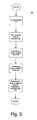
- FIG. 3shows a method for fabricating a transistor having passivated metal-semiconductor junctions from the source to the channel and from the channel to the drain, according to one embodiment of the present invention.
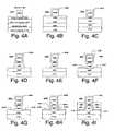
- FIGS. 4A-4Ishow intermediate substrates representing fabrication of a transistor having passivated aluminum-silicon junctions formed from an aluminum source to a silicon channel and from the silicon channel to an aluminum drain, according to one embodiment of the present invention.
- FIG. 5Aillustrates portions of a conventional FinFET device.
- FIG. 5Billustrates portions of a FinFET device having interface layers between the source/drain and the channel in accordance with an embodiment of the present invention.
- FIG. 6Aillustrates portions of a conventional vertical MOSFET device.
- FIG. 6Billustrates portions of a vertical MOSFET device having interface layers between the source/drain and the channel in accordance with an embodiment of the present invention.
- FIG. 7Aillustrates portions of a conventional MESFET device.
- FIG. 7Billustrates portions of a MESFET device having an interface layer between the gate and the channel in accordance with an embodiment of the present invention.
- FIG. 8illustrates the operation of different n-type devices having tunnel barriers in accordance with an embodiment of the present invention under various gate voltage conditions.
- the above-cited co-pending patent applicationdescribes processes for depinning the Fermi level of a silicon-based or germanium semiconductor (e.g., Si, SiC, SiGe, SiGeC, or Ge) at a metal-semiconductor junction as well as devices that use such a junction.
- a silicon-based or germanium semiconductore.g., Si, SiC, SiGe, SiGeC, or Ge
- an interface layeris introduced between the semiconductor and the metal.
- the interface layerfunctions to passivate the semiconductor surface (that is, terminate dangling bonds that may otherwise be present at the semiconductor surface so as to assure chemical stability of the surface) and to displace the semiconductor from the metal so as to reduce the effect of MIGS.
- minimum specific contact resistancesof less than or equal to approximately 1000 ⁇ - ⁇ m 2 or less than or equal to approximately 100 ⁇ - ⁇ m 2 or less than or equal to approximately 50 ⁇ - ⁇ m 2 or less than or equal to approximately 10 ⁇ - ⁇ m 2 or even less than or equal to approximately 1 ⁇ - ⁇ m 2 may be achieved for such junctions in accordance with the present invention.
- FIG. 8Shown in the illustration is a 2 ⁇ 2 grid of band diagrams.
- the upper two diagramsillustrate the operation of an n-type device having tunnel barriers (in the form of an interface layer configured in accordance with the present invention) and a metal source/drain in which the workfunction is aligned to the semiconductor channel conduction band under different gate voltages. Notice that the device is OFF (i.e., not conducting current) when the gate-to-source voltage (V GS ) is 0. The device is ON (i.e., conducting current) when V GS >0.
- the lower two diagramsillustrate the operation of the n-type device having a metal source/drain in which the workfunction is aligned to the semiconductor channel mid-gap. Notice that even in the ON state ON (i.e., V GS >0) a barrier to current flow exists due to band bending. This results in a higher contact resistance.
- the interface layers described in the above-cited patent applicationmay be used in connection with a semiconductor surface of a channel in a FET, as discussed below. That is, an interface layer may be disposed between a source and a channel, a channel and a drain, or both of an insulated gate field effect transistor. Such use of an interface layer is described in detail herein.
- the present inventionprovides a source—channel and/or channel—drain contact wherein the Fermi level of the source and/or drain metal is aligned (or approximately aligned) with the conduction or valence band of the semiconductor, depending on the type of semiconductor material and metals used.
- the junction of the present inventioncan be used in making contacts to source or drain implanted wells and will have the advantage of reducing the need for high doping levels (which are now reaching their limits of solid solubility).
- the high doping profileswere required in the past in order to keep the junction depletion layer relatively thin, so as to increase the tunneling current, thus reducing the junction resistance.
- the present inventionis used with high doping levels, the resistance will be further reduced.
- the present inventorshave devised a scheme to passivate a semiconductor surface such as a channel surface within a Schottky barrier transistor.
- the schemeinvolves forming a passivation layer which is a nitride, hydride, oxide, arsenide and/or fluoride of the semiconductor that makes up the channel.
- a passivation layerwhich is a nitride, hydride, oxide, arsenide and/or fluoride of the semiconductor that makes up the channel.
- the term interface layerwill be used in connection with the present invention to include passivation layers alone and passivation layers in combination with separation layers, where such separation layers are appropriate.
- the interface layerchemically neutralizes and physically protects the semiconductor channel surface.
- the interface layeralso allows for a tunable Schottky barrier, having a height that depends on bulk characteristics of the channel semiconductor and the source/drain metal, rather than on surface properties. This allows greater control over the barrier height to meet the operational characteristics that are desired for the transistor.
- This schemediffers from past attempts by others to insulate channel surfaces and provide adjustable Schottky barriers in that the passivation materials used for the interface layer are not limited to metals that readily form silicides with the semiconductor channel.
- the present inventiondecouples the need for semiconductor passivation from other considerations used to select the source/drain metal, such as the desirability of a particular workfunction. It further provides for greater control of the Schottky-barrier height than previously possible.
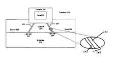
- FIG. 2shows a transistor 200 formed on a substrate 210 (e.g., a semiconductor substrate such as Si or a compound substrate such as SOI) and configured in accordance with an embodiment of the present invention.
- the transistor 200contains a channel 220 that is separated from a source 250 and a drain 260 by interface layers 230 and 240 , respectively, each of which form passivated Schottky barriers.
- the particular transistor 200 shown, which is one example of a switching device,is an Insulated Gate FET.
- the interface layers 230 and 240passivate the surfaces of channel 220 in the regions of the source/drain—channel junctions by chemically stabilizing the channel surface.
- the interface layers 230 and 240also reduce or eliminate the effect of MIGS in the region of the source/drain—channel junctions by displacing the source/drain ( 250 / 260 ) away from the channel 220 .
- the result of introducing the interface layers 230 and 240 between the semiconductor channel 220 and the metal source/drain 250 / 260is a depinning of the Fermi level of the semiconductor that makes up channel 220 .
- the height of the Schottky barrierwill depend only on the difference of the bulk workfunctions of the metal and the semiconductor in contact at the junction, and will not be dependent upon the interface.
- the reduction in the effectiveness of the MIGS to pin the Fermi leveldepends on the choice of interface dielectric.
- MIGSmetal-oxide-semiconductor
- dielectricshave much weaker MIGS than semiconductors, primarily due to larger bandgaps.
- the choice of dielectricis important in determining the final electrical characteristics of the Schottky barrier junction.
- the transistor 200also includes a gate 270 surrounded by an insulator 280 .
- the terms gate, source and draineach refer to terminals of a three terminal Insulated Gate FET.
- the source 250 and drain 260are the terminals between which conduction occurs under the influence of an electric field resulting from a voltage applied to the gate 270 .
- the source 250 and the drain 260are provided at opposite ends of the channel 220 so that the channel 220 is disposed between the source 250 and the drain 260 .
- the source 250 and drain 260are fabricated such that they are geometrically symmetrical. Symmetrical source and drain terminals may be referred to as source/drain terminals.
- a particular terminalmay be designated a source or a drain on the basis of the voltage to be applied to that terminal when the FET is operated in an electrical circuit.
- the source 250is provided at a left-hand side of the channel 220 and the drain 260 is provided at a right-hand side of the channel 220 , although another embodiment is contemplated wherein the source 250 and the drain 260 are interchanged.
- the source 250 and the drain 250may each contain a conductor, preferably a metal.
- metalsthat may be used include pure metals, alloys, refractory metals, metals that do not form silicides, and metals having a predetermined work function.
- the gate 270which may also preferably contain a conductor, such as a metal, is located above the channel 220 and is capacitively coupled to the channel 220 through the insulator 280 . Note, in other embodiments the transistor's three terminals may be coplanar or the gate 270 may be disposed below the level of the source 250 and/or the drain 260 in the substrate 210 .
- the insulator 280(which may be made of a dielectric such as an oxide of the metal gate or an oxide of a semiconductor) surrounds the gate 270 and separates the gate 270 from the source 250 , the drain 260 , the channel 220 , and the interface layers 230 and 240 .
- the insulator 280is of a sufficient thickness to provide a high resistance between the gate 270 and the channel 220 such that essentially no current flows between the gate 270 and the channel 220 .
- the resistancemay be between about 10 8 Ohms and about 10 12 Ohms, or greater. Such a resistance may allow the gate 270 and the channel 220 to be capacitively coupled, while preventing current from flowing between the gate 270 and the channel 220 .
- the insulator 280may also or alternatively contain a high-k dielectric material that has a higher dielectric constant than that of silicon dioxide (i.e., higher than about 4.0).
- the high-k materialmay allow the same charge induced in the channel 220 under the gate 270 to be achieved at the same gate voltage in a thicker layer. That is, the higher dielectric constant may allow the insulator 280 to have a greater layer thickness than a corresponding layer of silicon dioxide that provides the same amount of insulation. The increased thickness may simplify fabrication of the transistor 200 .
- the thicker layermay also have less leakage current than a thinner SiO 2 layer.
- Exemplary high-k dielectric materialsthat are contemplated include materials having a dielectric constant greater than about 4 (e.g., zinc oxide, ZnO), greater than about 10 (e.g., aluminum oxide, Al 2 O 3 ), greater than about 20 (e.g., zirconium oxide, ZrO 2 ), and greater than about 40 (e.g., hafnium oxide, HfO).
- a dielectric constantgreater than about 4 (e.g., zinc oxide, ZnO), greater than about 10 (e.g., aluminum oxide, Al 2 O 3 ), greater than about 20 (e.g., zirconium oxide, ZrO 2 ), and greater than about 40 (e.g., hafnium oxide, HfO).
- the channel 220contains a semiconductor material.
- semiconductoris used to refer to a material having a bandgap that is greater than about 0.1 electron volts and less than about 4 electron volts.
- Exemplary semiconductors that are contemplatedinclude Si, Ge, SiGe or SiC.
- the semiconductor materialmay have a wide range of doping levels including no doping at all.
- the interface layers 230 and 240each contain a passivation material that provides passivation to the channel 220 by covalently bonding with a dangling bond of a surface semiconductor atom to fully coordinate the semiconductor atom and thereby help passivate the semiconductor atom.
- the passivation materialis preferably selected from the group consisting of a hydride, a nitride, an arsenide, an oxide and a fluoride of the semiconductor channel 220 .
- a separation layer 242in addition to a passivation layer 244 within the interface layers may be needed.
- the combination of the passivation layer and the separation layermust be sufficiently thin to permit the low specific contact resistances described in the above-cited patent application. Further details regarding the formation of an interface layer may be found in the above-cited patent application and will not be repeated herein.
- FIG. 3shows a method 300 for fabricating a transistor having passivated metal-semiconductor junctions from the source to the channel and from the channel to the drain, according to one embodiment of the present invention.
- the methodstarts at block 301 and then proceeds to block 310 where a substrate is provided.
- an insulated gate structureis formed on the substrate.
- the insulated gate structuremay contain a gate having a conductive material (e.g., a metal) and a gate insulator having an insulating material beneath the conductive material.
- a channelis formed under the insulated gate.
- the channelmay include undercut void regions subjacent the gate dielectric and extending into the channel on both ends of the insulated gate structure.
- the methodadvances to block 340 where an interface layer is formed on the channel sides.
- Forming the interface layermay include creating a passivating layer and (where necessary) a separation layer using one or more of the materials discussed above.
- the methodthen advances to block 350 where a source and drain are formed on opposite sides of the channel, including on the interface layer, and within any undercut regions. Depending upon the interface layer thickness and robustness, the source and drain may be formed by substantially non-invasive approaches.
- the methodterminates at block 360 .
- FIGS. 4A-Ishow intermediate substrates, representing fabrication of the transistor shown in FIG. 4I, according to one embodiment of the present invention.
- the particular transistor shown in FIG. 4Icontains passivated aluminum-silicon junctions 482 I and 484 I formed from the aluminum source 492 I to the silicon channel 430 I and from the silicon channel 430 I to the aluminum drain 494 I.
- thisis merely one example of a transistor configured in accordance with the present invention.
- planar deviceswherein the gate, source and drain are co-planar in or above the substrate are also within the scope of the present invention, as are embodiments where the gate is disposed in a plane below the source and/or drain.
- embodiments wherein the width of the gate is less than the width of the channelare included within the present invention.
- FIGS. 4A-Itherefore show one embodiment of fabricating a transistor, according to the method 300 .
- FIGS. 4A-4Cshow providing a substrate and forming an insulated gate on the substrate.
- FIGS. 4D-4Eshow forming a channel beneath the insulated gate, such that the channel and the insulated gate define a first and a second undercut void region that extend underneath the insulated gate toward the channel from a first and a second side of the insulated gate.
- FIG. 4Gshows forming an interface layer on exposed sidewall surfaces of the channel.
- FIGS. 4F, 4 G, and 4 Hshow forming a source and a drain terminal on a first and a second side of the channel including on the interface layers, and forming extension tips within the undercut voids beneath the insulated gate.
- FIG. 4Ashows a first intermediate substrate 400 A containing a silicon substrate 410 A, a layer of buried oxide of silicon 420 A, a layer of silicon on insulator 430 A, a layer of an oxide of silicon 440 A, and an aluminum gate 450 A.
- the layers 410 A- 430 Arepresent a conventional Silicon On Insulator (SOI) substrate.
- SOI substrateincludes the buried layer 440 A to help isolate proximate semiconductor devices formed in the layer of silicon on insulator. This isolation may help reduce short-channel effects, as compared to semiconductor devices formed in a bulk wafer.
- the buried oxide layermay have a thickness that is effective to isolate the silicon on insulator, preferably greater than about 10 nm.
- the layer of silicon on insulatormay have a thickness of about 20 nm, or slightly less.
- the SOI substrateis not a limitation of the present invention.
- Other substratesare contemplated to replace the SOI substrate.
- the SOI substratemay be replaced by a Silicon-On-Sapphire substrate, although this may increase the cost of fabrication, or the SOI substrate may be replaced by a plain silicon wafer, although this may provide inferior electrical isolation of semiconductor devices and poor short-channel characteristics.
- the layer of oxide of silicon 440 Ain one embodiment silicon dioxide (SiO 2 ), may be formed by wet or dry oxidation of the silicon on insulator, as is common in the semiconductor processing arts.
- the layermay be sufficiently thin to serve as a gate oxide and have a thickness between about 1 nm and about 10 nm.
- the aluminum gate 450 Ais formed on the oxide 440 A.
- the aluminum gatehas a width 451 A that is about equal to, or slightly larger than the intended channel length, which in one embodiment is less than about 50 nm and in another embodiment is less than about 20 nm. More than slight increases of the width over the channel length may increase the extent and angle of a subsequent undercut etch, which may complicate fabrication.
- the gate 450 Amay be formed by depositing a layer of aluminum on the oxide 440 A, depositing a photoresist layer on the deposited aluminum layer, exposing a pattern including the width 451 A in the photoresist using conventional high-resolution lithography, removing a portion of the photoresist according to the exposed pattern, wet or dry etching a portion of the deposited layer of aluminum according to the patterned photoresist, and removing the remaining photoresist.
- FIG. 4Bshows a second intermediate substrate 400 B containing an oxide of aluminum insulator 460 B formed on exposed portions, including the top and sides, of the aluminum gate 450 B.
- the oxide of aluminum layer 460 Bmay have a thickness between about 1 nm and about 20 nm. The thickness may be about equivalent to the thickness of the layer 440 B, or slightly larger. Larger thickness may improve performance by reducing capacitance between the gate and the source, however the additional thickness may also increase fabrication complexity by increasing undercut.
- Forming the oxide of aluminum layer 460 Bmay include oxidizing the aluminum gate 450 A in an oxygen plasma etcher that provides a suitable oxidizing atmosphere, or by other methods known in the semiconductor processing arts.
- FIG. 4Cshows a third intermediate substrate 400 C containing a gate oxide 440 C formed by removing a portion of the layer 440 B that is not beneath aluminum gate 450 B or aluminum oxide 460 B.
- the removalmay include using the oxidized aluminum gate 450 B- 460 B as a mask for the layer 440 B and etching portions of the layer 440 B that are not subjacent to and concealed by the oxidized aluminum gate 450 B- 460 B. This removal leaves a portion of the silicon on insulator layer 430 C that is not subjacent to the gate oxide 440 C, aluminum gate 450 C, or oxide 460 C exposed.
- Etchingmay include Reactive Ion Etching (RIE) to encourage etching preferentially in the direction normal or perpendicular to the surface of the layer 440 B.
- RIEReactive Ion Etching
- RIEis a dry-etch process wherein the intermediate substrate 400 B is placed on a radio frequency powered electrode and provided with a potential that helps ionize and accelerate ion bombardment of etching species extracted from plasma toward the etched surface.
- FIG. 4Dshows a fourth intermediate substrate 400 D containing a silicon channel 430 D formed by removing a portion of the silicon on insulator layer 430 C that is substantially not subjacent and concealed by the gate oxide 440 C. Removal may include etching silicon on insulator that has a standard Si-100 orientation with tetramethylammonium hydroxide (TMAH) to form angled sidewalls that slope inward toward the gate 450 D, as shown. Alternatively, comparatively straight sidewalls aligned with the gate oxide 440 D may be formed by a self-limiting etch in TMAH if the silicon on insulator has a Si-110 orientation. Such comparatively straight sidewalls may also be formed by RIE.
- TMAHtetramethylammonium hydroxide
- FIG. 4Eshows a fifth intermediate substrate 400 E containing an undercut silicon channel 430 E formed by removing a portion of the channel 430 D that is subjacent and aligned with the gate oxide 440 D.
- the undercut silicon channel 430 Econtains an undercut region wherein the silicon is removed from the channel 430 D at a left and right-hand edge of the gate oxide 440 D to allow a subsequent formation of source and drain material vertically under the gate oxide 440 E. Removal may be by a non-directional or isotropic wet silicon etch with TMAH wherein etching takes place in substantial uniform amounts along the sidewall.
- the TMAH etchmay not be completely self-limiting and may form an undercut due to the vertical ridges or stair steps of crystal structure.
- removalmay be by an isotropic RIE.
- FIG. 4Fshows a sixth intermediate substrate 400 F containing a seed layer 476 F, 472 F, and 474 F formed respectively on a top surface of the insulated gate and on a left and right-hand side of the insulated gate.
- the seed layerfacilitates subsequent formation of a metal source and drain.
- the seed layermay be deposited anisotropically so that no significant seed layer material is deposited on the vertical sidewalls of the aluminum oxide 460 F, gate oxide 440 F, or channel 430 F and essentially no metal is deposited on the underside of the undercut overhang of the gate oxide 440 F. This is desired to electrically isolate the seed layer portion 476 F from the seed layer portion 472 F and 474 F.
- the seed layercontains chromium deposited from a thermal source. Chromium provides desirable electrochemistry and is well suited for formation of ultra-thin films.
- FIG. 4Gshows a seventh intermediate substrate 400 G containing a modified seed layer 472 G- 474 G formed by selectively removing the layer portion 476 F from the top surface of the insulated gate. Removal of the portion 476 F is desirable to allow depositing the source and drain materials superjacent the layer portions 472 G and 476 G without depositing the source and drain materials atop the oxidized aluminum gate structure. Since the seed layer portion 476 F is electrically isolated from the seed layer portions 472 F and 476 F, the portion 476 F may be removed electrochemically by a Cerric Ammonium Nitrate (CAN) chrome etch.
- CANCerric Ammonium Nitrate
- the seed layer portions 472 F and 474 F but not the seed layer portion 476 Fmay be electrically coupled with a copper electrical probe at the edge of the substrate to etch the seed layer portion 476 F but not the portions 472 F- 474 F.
- patterningmay be used to form chromium layers 472 F and 474 F without forming chromium layer 476 F. This may avoid a subsequent removal of the chromium layer 476 F.
- FIG. 4Hshows an eighth intermediate substrate 400 H containing interface layers 482 H and 484 H formed on the sidewall surfaces of the channel 430 H.
- the interface layersmay be a monolayer, slightly more than a monolayer, less than about 0.3 nm, less than about 0.5 nm or less than about 1 nm (depending upon the desired Schottky barrier characteristics). That is, in some cases an amount of passivation material sufficient to terminate all or a sufficient number of dangling bonds of the semiconductor channel to achieve chemical stability of the surface may be used.
- the interface layersmay be grown in accordance with the techniques discussed in the above-cited patent application. Passivation materials that are contemplated include arsenic, hydrogen, fluorine, oxygen, and nitrogen, as discussed above, and the interface layers 482 H and 484 H may be made up of both a passivation layer and a separation layer.
- FIG. 4Ishows a ninth intermediate substrate 400 I containing a source 492 I formed superjacent upon the seed material 472 H and beneath the left undercut overhang and a drain 494 I formed superjacent upon the seed material 474 H and beneath the right undercut overhang.
- the source and drainhave a thickness that extends above the gate insulator 440 I. Desirably, the thickness may be precisely controlled. Forming may include plating the potentially different source/drain materials on the seed layers 472 H and 474 H.
- Thismay include depositing a photoresist, irradiating the photoresist to expose a channel width pattern, removing a portion of the photoresist to expose the seed layers 472 H and 474 H, plating the source/drain materials on the seed layers 472 H and 474 H, and removing the remainder of the photoresist.
- the source and drain materialsare aluminum.
- the source and drain materialsmay be another desired and potentially different metal or alloy.
- the transistor shown in FIG. 4Ihas a number of advantages.
- the transistorprovides a simple construction. This may allow extending transistor fabrication below 50 nm channel lengths, below 20 nm channel lengths, or even below 10 nm channel lengths.
- Another advantageis greater control over the Schottky barrier height provided by the interface layers.
- the barrier heightmay be controlled by the properties of the interface layer such as passivation material, layer thickness, and layer formation conditions, in addition to difference in workfunctions between the source/drain and the channel. This ability to control the barrier height is further increased by greater flexibility in selecting source/drain materials, since, due to the interface layers, the source/drain materials do not have to readily form silicides with the silicon channel.
- the channel—interface layer—source/drain junction(s) of the transistor shown in FIG. 4Iare unique in that the Fermi level of the semiconductor channel is depinned in a region near the junction and the junction has a specific contact resistance of less than approximately 1000 ⁇ - ⁇ m 2 . This is true of all transistors configured in accordance with the present invention. Indeed, minimum specific contact resistances of less than or equal to approximately 10 ⁇ - ⁇ m 2 or even less than or equal to approximately 1 ⁇ - ⁇ m 2 may be achieved for such junctions in accordance with the present invention.
- a source/drain metalthat has a work function near the conduction band of the semiconductor for n-type semiconductors, or a work function that is near the valence band for p-type semiconductors, is selected.
- the depinning role played by the interface layer in tuning, adjusting, or controlling the height of the barrier between the source/drain and the semiconductor channelinvolves both a reduction in surface states of the channel, by bonding to the semiconductor material to consume dangling bonds, a reduction in the formation of MIGS in the semiconductor channel, by providing a thickness and bandgap that prevent the electron wave function (of the source/drain metal) from penetrating into the semiconductor channel.
- the electron wave functionmay instead penetrate into the interface layer and form MIGS within the interface layer at an energy related to the states of the interface layer material.
- the density of the MIGS and the depth of MIGS penetration into the interface layermay be reduced by choosing an interface layer material or materials having a larger bandgap or higher effective mass than the semiconductor of the channel.
- the interface layeris operable to pass current to/from the semiconductor channel during device operation.
- an interface layerhaving a thickness of a monolayer, or, for example between about 0.1 nm and about 0.3 nm, and also having a wide bandgap (as compared to that of the semiconductor of the channel) so that the interface layer both depins the Fermi level (so that the barrier height depends predominantly on bulk properties of the junction materials) and allows sufficient current transfer across it.
- the interface layermay include only an amount of passivation material sufficient to terminate all or a sufficient number of dangling bonds of the semiconductor channel to achieve chemical stability of the surface.
- such interface layersmay be sufficiently thin to provide low impedance to current flow (due to the exponential dependence of direct tunneling on barrier thickness), which is desirable for many semiconductor devices, while also providing sufficient semiconductor surface passivation to allow an adjustable barrier height. That is, the interface layer may allow passivation of surface states and reduction (or elimination) of MIGS in the semiconductor to allow for an adjustable barrier height with a substantially thin layer that allows sufficient current to be transferred across the interface layer.
- the barrier heightcan be made adjustable.
- adjustmentmay be made by tuning the degree of Fermi level pinning.
- some embodimentsmay allow for a sufficiently thin interface layer so that not all of the effects of MIGS in the semiconductor channel are eliminated.
- the pinningmay be varied by combinations of thickness of the interface layer and the choice of interface material.
- the metal in contact with the interface layermay be pinned by MIGS at different levels in different materials.
- the semiconductor channel passivationmay be left incomplete to allow for an effective level of unpassivated states.
- Complete depinning of the Fermi levelthat is removal of all surface states in the semiconductor channel including MIGS is another option, in which case one could tune the barrier height simply by choosing a pure metal or an alloy that possesses the desired workfunction.
- one embodiment for fabricating a transistor on a semiconductor substrateincludes: (1) forming a semiconductor oxide dielectric layer on a semiconductor substrate by oxidizing the semiconductor substrate; (2) forming a metal gate on the semiconductor oxide layer by depositing a layer of metal on the semiconductor oxide and removing a portion of the deposited layer of metal based on a lithographic exposure; (3) forming a metal oxide dielectric layer on exposed portions of the metal gate by oxidizing the metal gate; (4) forming a gate oxide dielectric by removing a portion of the semiconductor oxide layer that is protected by the metal oxide formed on the metal gate; (5) forming a semiconductor channel structure by removing a portion of the semiconductor substrate that is not protected by the metal oxide formed on the metal gate; (6) forming an undercut semiconductor channel containing a source undercut region for a source tip and a drain undercut region for a drain tip by removing a source tip portion of the semiconductor channel structure that is subjacent to a left-hand end of the gate oxide and extends underneath the gate oxide toward the channel top
- the transistor illustrated in FIG. 4Iis but one example of the types of FETs that can benefit from the present invention.
- Other FETs known in the artmay also realize such benefits by incorporating the present interface layers into source/drain—channel junctions.
- so-called FinFETsmay incorporate such interface layers.
- a FinFETis an example of a thin-body SOI device and is the name given to a class of FETs developed by researchers at the University of California, Berkely.
- Conventional FinFETsare described in detail in Yang-Kyu Choi et al., “Nanoscale CMOS Spacer FinFET for the Terabit Era”, IEEE Electron Device Letters, vol. 25, no. 1 (January 2002), incorporated herein by reference, and an example of such a device 500 is illustrated in FIG. 5 A.
- the channel of a finFETis formed by spacer-defined semiconductor fins.
- FIG. 5Bshows a Fin-FET 520 modified to incorporate interface layers 522 in accordance with an embodiment of the present invention.
- the semiconductor source and/or drainare replaced with a metal source and/or drain.
- the semiconductor finsi.e., the channel
- the semiconductor finscontact these source/drain regions through an interface layer.
- FIG. 6 AAnother transistor where the present invention may find application is the so-called vertical MOSFET, e.g., as described in E. Josse et al., “High performance 40 nm vertical MOSFET within a conventional CMOS process flow”, 2001 Symposium on VLSI Technology Digest of Technical Papers. Paper No. 5B-2, pages 55-56 (2001), incorporated herein by reference.
- Vertical MOSFETsare characterized by a pillar-like channel sandwiched between a double gate. The source and drain are located at the ends of the channel pillar. An example of such a structure 600 is shown in FIG. 6 A.
- FIG. 6Bshows a vertical MOSFET 620 modified to incorporate interface layers in accordance with an embodiment of the present invention.
- This transistoris similar to the MOSFET illustrated in FIG. 6A but the upper Si n-region (the drain in this example) has been replace with a metal drain and contact to the channel is through an interface layer 622 .
- such devicesmay be asymmetric, having a passivated Si/metal tunnel junction at the top contact, and a Si p-n junction at the bottom of the device on the substrate side.
- Complementary devicesmay be fabricated on the same substrate by first implanting p and n regions for the bottom contacts, and then employing two different metals, each with work functions chosen to yield p-type or n-type devices, as the top contacts to the channel.
- FIG. 7Aillustrates yet another type of transistor 700 , the MESFET.
- a MESFETMetal Semiconductor FET replaces the gate/insulator/semiconductor stack adjacent to the channel with a metal/semiconductor contact, intentionally forming a Schottky barrier.
- the conductance of the channelis modulated when an applied gate voltage results in a change in the depletion width of the Schottky barrier into the channel.
- the channel as shownmay be a thin Si layer, as in an SOI substrate.
- the Schottky barrierFor optimizing the utility of a particular MESFET application, it may be desirable to either raise or lower the Schottky barrier. This may be achieved as shown in FIG. 7B by implementation of the present invention in a transistor 720 wherein a particular interface dielectric and contact metal may be appropriately chosen.
- the interface dielectricforms an interface layer 722 between the gate and the channel.
- the gatemay be poly Si instead of a metal.
- Transistorssuch as those described herein may be used in chips, integrated circuits, monolithic devices, semiconductor devices, microelectronic devices, and the like within a number of electrical systems. Electrical systems that are contemplated include computer systems (e.g., portable, laptop, desktop, server, mainframe, etc.), hard copy equipment (e.g., printer, plotter, fax machine, etc.), and other electrical systems.
- a computer systemmay comprise a microprocessor having such a transistor to help execute instructions.
- the computer systemmay contain other conventional components including but not limited to a bus or other communication means to communicate information, a memory to store information (e.g., a dynamic memory such as RAM or a static memory such as ROM), a display device, a data input device, and a communication device such as a modem, as will be appreciated by a person having an ordinary level of skill in the art and the benefit of the present disclosure. Any or all of these devices may include transistors configured in accordance with the present invention.
- transistors having passivated junctions from the source to the channel and/or from the channel to the drainand a method for forming such a transistor have been described.
- metals other than aluminummay be used in transistors configured in accordance with the present invention.
- Low work function metals that may be so usedinclude Er, Eu, Ba, Cs, Ca, Ce, Rb, Sm, Y, and Yb. All have workfunctions less than 3 eV.
- High work function metalsfor aligning to valence bands
- Pthigh work function metals
- Irlow work function metals
- Pdhigh work function metals
- ReRe
- NiCo
- Augold
- the specification and drawingsare accordingly to be regarded in an illustrative rather than a restrictive sense and the invention measured only in terms of the claims, which follow.
Landscapes
- Engineering & Computer Science (AREA)
- Physics & Mathematics (AREA)
- Condensed Matter Physics & Semiconductors (AREA)
- General Physics & Mathematics (AREA)
- Computer Hardware Design (AREA)
- Microelectronics & Electronic Packaging (AREA)
- Power Engineering (AREA)
- Manufacturing & Machinery (AREA)
- Thin Film Transistor (AREA)
- Insulated Gate Type Field-Effect Transistor (AREA)
- Electrodes Of Semiconductors (AREA)
- Junction Field-Effect Transistors (AREA)
Abstract
Description
Claims (32)
Priority Applications (16)
| Application Number | Priority Date | Filing Date | Title |
|---|---|---|---|
| US10/342,576US6833556B2 (en) | 2002-08-12 | 2003-01-14 | Insulated gate field effect transistor having passivated schottky barriers to the channel |
| AU2003255257AAU2003255257A1 (en) | 2002-08-12 | 2003-08-08 | Insulated gate field effect transistor having passivated schottky barriers to the channel |
| JP2004527994AJP4713884B2 (en) | 2002-08-12 | 2003-08-08 | Insulated gate field effect transistor with passive Schottky barrier to channel |
| KR1020057002426AKR101018103B1 (en) | 2002-08-12 | 2003-08-08 | Isolated Gate Field Effect Transistors with Passivating Schottky Barriers for Channels |
| CNB038194961ACN100557816C (en) | 2002-08-12 | 2003-08-08 | Insulated Gate Field Effect Transistor with Passivated Schottky Barrier to Channel |
| PCT/US2003/025057WO2004015782A1 (en) | 2002-08-12 | 2003-08-08 | Insulated gate field effect transistor having passivated schottky barriers to the channel |
| EP03785158.1AEP1535343B1 (en) | 2002-08-12 | 2003-08-08 | Insulated gate field effect transistor having passivated schottky barriers to the channel |
| TW092122031ATWI310608B (en) | 2002-08-12 | 2003-08-11 | Insulated gate field effect transistor having passivated schottky barriers to the channel |
| TW092122115ATWI327376B (en) | 2002-08-12 | 2003-08-12 | Method for deplnntng the fermi level of a semiconductor at an electrical junction and devices incorporating such junctions |
| US10/754,966US7112478B2 (en) | 2002-08-12 | 2004-01-09 | Insulated gate field effect transistor having passivated Schottky barriers to the channel |
| US11/010,048US7382021B2 (en) | 2002-08-12 | 2004-12-09 | Insulated gate field-effect transistor having III-VI source/drain layer(s) |
| US11/403,185US7883980B2 (en) | 2002-08-12 | 2006-04-11 | Insulated gate field effect transistor having passivated schottky barriers to the channel |
| US13/022,559US8377767B2 (en) | 2002-08-12 | 2011-02-07 | Insulated gate field effect transistor having passivated schottky barriers to the channel |
| US13/757,597US8916437B2 (en) | 2002-08-12 | 2013-02-01 | Insulated gate field effect transistor having passivated schottky barriers to the channel |
| US14/298,810US9583614B2 (en) | 2002-08-12 | 2014-06-06 | Insulated gate field effect transistor having passivated schottky barriers to the channel |
| US15/418,360US11043571B2 (en) | 2002-08-12 | 2017-01-27 | Insulated gate field effect transistor having passivated schottky barriers to the channel |
Applications Claiming Priority (2)
| Application Number | Priority Date | Filing Date | Title |
|---|---|---|---|
| US10/217,758US7084423B2 (en) | 2002-08-12 | 2002-08-12 | Method for depinning the Fermi level of a semiconductor at an electrical junction and devices incorporating such junctions |
| US10/342,576US6833556B2 (en) | 2002-08-12 | 2003-01-14 | Insulated gate field effect transistor having passivated schottky barriers to the channel |
Related Parent Applications (1)
| Application Number | Title | Priority Date | Filing Date |
|---|---|---|---|
| US10/217,758Continuation-In-PartUS7084423B2 (en) | 2002-08-12 | 2002-08-12 | Method for depinning the Fermi level of a semiconductor at an electrical junction and devices incorporating such junctions |
Related Child Applications (1)
| Application Number | Title | Priority Date | Filing Date |
|---|---|---|---|
| US10/754,966DivisionUS7112478B2 (en) | 2002-08-12 | 2004-01-09 | Insulated gate field effect transistor having passivated Schottky barriers to the channel |
Publications (2)
| Publication Number | Publication Date |
|---|---|
| US20040026736A1 US20040026736A1 (en) | 2004-02-12 |
| US6833556B2true US6833556B2 (en) | 2004-12-21 |
Family
ID=31720178
Family Applications (7)
| Application Number | Title | Priority Date | Filing Date |
|---|---|---|---|
| US10/342,576Expired - LifetimeUS6833556B2 (en) | 2002-08-12 | 2003-01-14 | Insulated gate field effect transistor having passivated schottky barriers to the channel |
| US10/754,966Expired - LifetimeUS7112478B2 (en) | 2002-08-12 | 2004-01-09 | Insulated gate field effect transistor having passivated Schottky barriers to the channel |
| US11/403,185Expired - Fee RelatedUS7883980B2 (en) | 2002-08-12 | 2006-04-11 | Insulated gate field effect transistor having passivated schottky barriers to the channel |
| US13/022,559Expired - Fee RelatedUS8377767B2 (en) | 2002-08-12 | 2011-02-07 | Insulated gate field effect transistor having passivated schottky barriers to the channel |
| US13/757,597Expired - LifetimeUS8916437B2 (en) | 2002-08-12 | 2013-02-01 | Insulated gate field effect transistor having passivated schottky barriers to the channel |
| US14/298,810Expired - Fee RelatedUS9583614B2 (en) | 2002-08-12 | 2014-06-06 | Insulated gate field effect transistor having passivated schottky barriers to the channel |
| US15/418,360Expired - Fee RelatedUS11043571B2 (en) | 2002-08-12 | 2017-01-27 | Insulated gate field effect transistor having passivated schottky barriers to the channel |
Family Applications After (6)
| Application Number | Title | Priority Date | Filing Date |
|---|---|---|---|
| US10/754,966Expired - LifetimeUS7112478B2 (en) | 2002-08-12 | 2004-01-09 | Insulated gate field effect transistor having passivated Schottky barriers to the channel |
| US11/403,185Expired - Fee RelatedUS7883980B2 (en) | 2002-08-12 | 2006-04-11 | Insulated gate field effect transistor having passivated schottky barriers to the channel |
| US13/022,559Expired - Fee RelatedUS8377767B2 (en) | 2002-08-12 | 2011-02-07 | Insulated gate field effect transistor having passivated schottky barriers to the channel |
| US13/757,597Expired - LifetimeUS8916437B2 (en) | 2002-08-12 | 2013-02-01 | Insulated gate field effect transistor having passivated schottky barriers to the channel |
| US14/298,810Expired - Fee RelatedUS9583614B2 (en) | 2002-08-12 | 2014-06-06 | Insulated gate field effect transistor having passivated schottky barriers to the channel |
| US15/418,360Expired - Fee RelatedUS11043571B2 (en) | 2002-08-12 | 2017-01-27 | Insulated gate field effect transistor having passivated schottky barriers to the channel |
Country Status (8)
| Country | Link |
|---|---|
| US (7) | US6833556B2 (en) |
| EP (1) | EP1535343B1 (en) |
| JP (1) | JP4713884B2 (en) |
| KR (1) | KR101018103B1 (en) |
| CN (1) | CN100557816C (en) |
| AU (1) | AU2003255257A1 (en) |
| TW (2) | TWI310608B (en) |
| WO (1) | WO2004015782A1 (en) |
Cited By (15)
| Publication number | Priority date | Publication date | Assignee | Title |
|---|---|---|---|---|
| US20050087811A1 (en)* | 2003-10-07 | 2005-04-28 | United Microelectronics Corp. | Method for fabricating a double gate MOSFET device |
| US20060091467A1 (en)* | 2004-10-29 | 2006-05-04 | Doyle Brian S | Resonant tunneling device using metal oxide semiconductor processing |
| US20060197121A1 (en)* | 2005-03-04 | 2006-09-07 | Bae Systems Information And Electronic Systems Integration Inc. | Abrupt channel doping profile for fermi threshold field effect transistors |
| US20060226476A1 (en)* | 2005-01-21 | 2006-10-12 | Jun Suenaga | SiGe nickel barrier structure employed in a CMOS device to prevent excess diffusion of nickel used in the silicide material |
| US20070001223A1 (en)* | 2005-07-01 | 2007-01-04 | Boyd Diane C | Ultrathin-body schottky contact MOSFET |
| US20070007590A1 (en)* | 2003-09-05 | 2007-01-11 | Kabushiki Kaisha Toshiba | Field effect transistor and manufacturing method thereof |
| US20080023752A1 (en)* | 2006-07-28 | 2008-01-31 | International Business Machines Corporation | BORON DOPED SiGe HALO FOR NFET TO CONTROL SHORT CHANNEL EFFECT |
| US20080111163A1 (en)* | 2006-11-14 | 2008-05-15 | Infineon Technologies Ag | Field effect transistor with a fin structure |
| US7417257B2 (en) | 2003-12-05 | 2008-08-26 | International Rectifier Corporation | III-nitride device with improved layout geometry |
| US20110049630A1 (en)* | 2009-08-31 | 2011-03-03 | International Business Machines Corporation | Stressed Source/Drain CMOS and Method of Forming Same |
| US8217450B1 (en)* | 2004-02-03 | 2012-07-10 | GlobalFoundries, Inc. | Double-gate semiconductor device with gate contacts formed adjacent sidewalls of a fin |
| US8415722B2 (en) | 2004-07-28 | 2013-04-09 | Micron Technology, Inc. | Memory devices and memory cells |
| US9620611B1 (en) | 2016-06-17 | 2017-04-11 | Acorn Technology, Inc. | MIS contact structure with metal oxide conductor |
| WO2018094205A1 (en) | 2016-11-18 | 2018-05-24 | Acorn Technologies, Inc. | Nanowire transistor with source and drain induced by electrical contacts with negative schottky barrier height |
| US20210135007A1 (en)* | 2005-06-15 | 2021-05-06 | Intel Corporation | Method for fabricating transistor with thinned channel |
Families Citing this family (133)
| Publication number | Priority date | Publication date | Assignee | Title |
|---|---|---|---|---|
| US6303479B1 (en)* | 1999-12-16 | 2001-10-16 | Spinnaker Semiconductor, Inc. | Method of manufacturing a short-channel FET with Schottky-barrier source and drain contacts |
| US7190008B2 (en) | 2002-04-24 | 2007-03-13 | E Ink Corporation | Electro-optic displays, and components for use therein |
| US6835619B2 (en)* | 2002-08-08 | 2004-12-28 | Micron Technology, Inc. | Method of forming a memory transistor comprising a Schottky contact |
| US7084423B2 (en) | 2002-08-12 | 2006-08-01 | Acorn Technologies, Inc. | Method for depinning the Fermi level of a semiconductor at an electrical junction and devices incorporating such junctions |
| US7176483B2 (en)* | 2002-08-12 | 2007-02-13 | Acorn Technologies, Inc. | Method for depinning the Fermi level of a semiconductor at an electrical junction and devices incorporating such junctions |
| US7902029B2 (en)* | 2002-08-12 | 2011-03-08 | Acorn Technologies, Inc. | Process for fabricating a self-aligned deposited source/drain insulated gate field-effect transistor |
| US6833556B2 (en) | 2002-08-12 | 2004-12-21 | Acorn Technologies, Inc. | Insulated gate field effect transistor having passivated schottky barriers to the channel |
| KR100498475B1 (en)* | 2003-01-07 | 2005-07-01 | 삼성전자주식회사 | Mosfet structure and method of fabricating the same |
| US20070262363A1 (en)* | 2003-02-28 | 2007-11-15 | Board Of Regents, University Of Texas System | Low temperature fabrication of discrete silicon-containing substrates and devices |
| KR100508548B1 (en)* | 2003-04-16 | 2005-08-17 | 한국전자통신연구원 | Schottky barrier transistor and method for fabricating the same |
| US6894326B2 (en)* | 2003-06-25 | 2005-05-17 | International Business Machines Corporation | High-density finFET integration scheme |
| US7456476B2 (en) | 2003-06-27 | 2008-11-25 | Intel Corporation | Nonplanar semiconductor device with partially or fully wrapped around gate electrode and methods of fabrication |
| US6909151B2 (en) | 2003-06-27 | 2005-06-21 | Intel Corporation | Nonplanar device with stress incorporation layer and method of fabrication |
| US6995376B2 (en)* | 2003-07-01 | 2006-02-07 | International Business Machines Corporation | Silicon-on-insulator latch-up pulse-radiation detector |
| KR100496891B1 (en)* | 2003-08-14 | 2005-06-23 | 삼성전자주식회사 | Silicon fin for finfet and method for fabricating the same |
| JP2005064500A (en)* | 2003-08-14 | 2005-03-10 | Samsung Electronics Co Ltd | Multi-structure silicon fin and manufacturing method |
| JP2005086024A (en)* | 2003-09-09 | 2005-03-31 | Toshiba Corp | Semiconductor device and method for manufacturing same |
| US20050139860A1 (en)* | 2003-10-22 | 2005-06-30 | Snyder John P. | Dynamic schottky barrier MOSFET device and method of manufacture |
| KR100574971B1 (en)* | 2004-02-17 | 2006-05-02 | 삼성전자주식회사 | Multi-gate structure semiconductor device and manufacturing method thereof |
| US7923782B2 (en)* | 2004-02-27 | 2011-04-12 | International Business Machines Corporation | Hybrid SOI/bulk semiconductor transistors |
| US7154118B2 (en) | 2004-03-31 | 2006-12-26 | Intel Corporation | Bulk non-planar transistor having strained enhanced mobility and methods of fabrication |
| US7504328B2 (en)* | 2004-05-11 | 2009-03-17 | National University Of Singapore | Schottky barrier source/drain n-mosfet using ytterbium silicide |
| US7579280B2 (en) | 2004-06-01 | 2009-08-25 | Intel Corporation | Method of patterning a film |
| US7229893B2 (en)* | 2004-06-23 | 2007-06-12 | Taiwan Semiconductor Manufacturing Company, Ltd. | Method and apparatus for a semiconductor device with a high-k gate dielectric |
| JP4837902B2 (en) | 2004-06-24 | 2011-12-14 | 富士通セミコンダクター株式会社 | Semiconductor device |
| US7042009B2 (en) | 2004-06-30 | 2006-05-09 | Intel Corporation | High mobility tri-gate devices and methods of fabrication |
| US7365015B2 (en)* | 2004-07-13 | 2008-04-29 | Lsi Logic Corporation | Damascene replacement metal gate process with controlled gate profile and length using Si1-xGex as sacrificial material |
| JP2006054423A (en)* | 2004-07-13 | 2006-02-23 | Toshiba Corp | Semiconductor device and manufacturing method thereof |
| US7279756B2 (en)* | 2004-07-21 | 2007-10-09 | Taiwan Semiconductor Manufacturing Company, Ltd. | Semiconductor device with high-k gate dielectric and quasi-metal gate, and method of forming thereof |
| US7348284B2 (en) | 2004-08-10 | 2008-03-25 | Intel Corporation | Non-planar pMOS structure with a strained channel region and an integrated strained CMOS flow |
| US7345309B2 (en)* | 2004-08-31 | 2008-03-18 | Lockheed Martin Corporation | SiC metal semiconductor field-effect transistor |
| US7527994B2 (en)* | 2004-09-01 | 2009-05-05 | Honeywell International Inc. | Amorphous silicon thin-film transistors and methods of making the same |
| US7078722B2 (en) | 2004-09-20 | 2006-07-18 | International Business Machines Corporation | NFET and PFET devices and methods of fabricating same |
| US7422946B2 (en) | 2004-09-29 | 2008-09-09 | Intel Corporation | Independently accessed double-gate and tri-gate transistors in same process flow |
| JP2006100600A (en)* | 2004-09-29 | 2006-04-13 | Toshiba Corp | Semiconductor device and manufacturing method thereof |
| US7332439B2 (en) | 2004-09-29 | 2008-02-19 | Intel Corporation | Metal gate transistors with epitaxial source and drain regions |
| US7361958B2 (en) | 2004-09-30 | 2008-04-22 | Intel Corporation | Nonplanar transistors with metal gate electrodes |
| US20060086977A1 (en) | 2004-10-25 | 2006-04-27 | Uday Shah | Nonplanar device with thinned lower body portion and method of fabrication |
| US7355235B2 (en)* | 2004-12-22 | 2008-04-08 | Taiwan Semiconductor Manufacturing Company, Ltd. | Semiconductor device and method for high-k gate dielectrics |
| US7332407B2 (en)* | 2004-12-23 | 2008-02-19 | Taiwan Semiconductor Manufacturing Company, Ltd. | Method and apparatus for a semiconductor device with a high-k gate dielectric |
| US7518196B2 (en) | 2005-02-23 | 2009-04-14 | Intel Corporation | Field effect transistor with narrow bandgap source and drain regions and method of fabrication |
| FR2883101B1 (en)* | 2005-03-08 | 2007-06-08 | Centre Nat Rech Scient | NANOMETRIC MOS TRANSISTOR WITH MAXIMIZED CURRENT TO CURRENT AND CURRENT STATE RATE |
| US20060202266A1 (en) | 2005-03-14 | 2006-09-14 | Marko Radosavljevic | Field effect transistor with metal source/drain regions |
| US7329937B2 (en)* | 2005-04-27 | 2008-02-12 | International Business Machines Corporation | Asymmetric field effect transistors (FETs) |
| US7176537B2 (en)* | 2005-05-23 | 2007-02-13 | Taiwan Semiconductor Manufacturing Company, Ltd. | High performance CMOS with metal-gate and Schottky source/drain |
| US7547637B2 (en) | 2005-06-21 | 2009-06-16 | Intel Corporation | Methods for patterning a semiconductor film |
| US7279375B2 (en) | 2005-06-30 | 2007-10-09 | Intel Corporation | Block contact architectures for nanoscale channel transistors |
| US7402875B2 (en) | 2005-08-17 | 2008-07-22 | Intel Corporation | Lateral undercut of metal gate in SOI device |
| US7479421B2 (en) | 2005-09-28 | 2009-01-20 | Intel Corporation | Process for integrating planar and non-planar CMOS transistors on a bulk substrate and article made thereby |
| US20070090416A1 (en) | 2005-09-28 | 2007-04-26 | Doyle Brian S | CMOS devices with a single work function gate electrode and method of fabrication |
| US7485503B2 (en) | 2005-11-30 | 2009-02-03 | Intel Corporation | Dielectric interface for group III-V semiconductor device |
| KR100777101B1 (en)* | 2005-12-07 | 2007-11-19 | 한국전자통신연구원 | Manufacturing Schottky-Barrier MOSFETs with low barrier height and manufacturing method thereof |
| JP2007165772A (en)* | 2005-12-16 | 2007-06-28 | Toshiba Corp | Semiconductor device and manufacturing method of semiconductor device |
| US7432526B2 (en)* | 2005-12-20 | 2008-10-07 | Palo Alto Research Center Incorporated | Surface-passivated zinc-oxide based sensor |
| US7396711B2 (en) | 2005-12-27 | 2008-07-08 | Intel Corporation | Method of fabricating a multi-cornered film |
| CN103219465B (en)* | 2006-01-09 | 2016-02-03 | 技术研究及发展基金有限公司 | Transistor arrangement and manufacture method thereof |
| US7473593B2 (en)* | 2006-01-11 | 2009-01-06 | International Business Machines Corporation | Semiconductor transistors with expanded top portions of gates |
| FR2897202B1 (en)* | 2006-02-08 | 2008-09-12 | St Microelectronics Crolles 2 | MOS TRANSISTOR WITH SCHOTTKY BARRIER ON SEMICONDUCTOR FILM ENTIRELY DEPLETED AND METHOD OF MANUFACTURING SUCH TRANSISTOR |
| WO2007101120A1 (en)* | 2006-02-23 | 2007-09-07 | Acorn Technologies, Inc. | Method for making semiconductor insulated-gate field-effect transistor having multilayer deposited metal source (s) and/or drain (s) |
| JP2007299951A (en)* | 2006-04-28 | 2007-11-15 | Toshiba Corp | Semiconductor device and manufacturing method thereof |
| US8435873B2 (en)* | 2006-06-08 | 2013-05-07 | Texas Instruments Incorporated | Unguarded Schottky barrier diodes with dielectric underetch at silicide interface |
| US7485524B2 (en)* | 2006-06-21 | 2009-02-03 | International Business Machines Corporation | MOSFETs comprising source/drain regions with slanted upper surfaces, and method for fabricating the same |
| US8143646B2 (en) | 2006-08-02 | 2012-03-27 | Intel Corporation | Stacking fault and twin blocking barrier for integrating III-V on Si |
| US20080258242A1 (en)* | 2007-04-19 | 2008-10-23 | Northrop Grumman Space And Mission Systems Corp. | Low contact resistance ohmic contact for a high electron mobility transistor and fabrication method thereof |
| JP2008288499A (en)* | 2007-05-21 | 2008-11-27 | Panasonic Corp | Semiconductor device and manufacturing method thereof |
| JP5108408B2 (en)* | 2007-07-26 | 2012-12-26 | ルネサスエレクトロニクス株式会社 | Semiconductor device and manufacturing method thereof |
| JP2009059996A (en)* | 2007-09-03 | 2009-03-19 | Univ Of Tokyo | Semiconductor device and manufacturing method thereof |
| KR100945508B1 (en) | 2007-11-16 | 2010-03-09 | 주식회사 하이닉스반도체 | Zero Capacitor Ram and Method of Manufacturing the Same |
| US8362566B2 (en) | 2008-06-23 | 2013-01-29 | Intel Corporation | Stress in trigate devices using complimentary gate fill materials |
| US8110877B2 (en) | 2008-12-19 | 2012-02-07 | Intel Corporation | Metal-insulator-semiconductor tunneling contacts having an insulative layer disposed between source/drain contacts and source/drain regions |
| JP4752927B2 (en)* | 2009-02-09 | 2011-08-17 | ソニー株式会社 | Thin film transistor and display device |
| JP5210915B2 (en)* | 2009-02-09 | 2013-06-12 | 株式会社東芝 | Manufacturing method of semiconductor device |
| JP5449326B2 (en)* | 2009-03-31 | 2014-03-19 | Jx日鉱日石金属株式会社 | Manufacturing method of Schottky junction FET |
| US8288803B2 (en)* | 2009-08-31 | 2012-10-16 | International Business Machines Corporation | Tunnel field effect devices |
| US20110049582A1 (en)* | 2009-09-03 | 2011-03-03 | International Business Machines Corporation | Asymmetric source and drain stressor regions |
| US8669644B2 (en)* | 2009-10-07 | 2014-03-11 | Texas Instruments Incorporated | Hydrogen passivation of integrated circuits |
| JP5640379B2 (en)* | 2009-12-28 | 2014-12-17 | ソニー株式会社 | Manufacturing method of semiconductor device |
| KR101121633B1 (en)* | 2009-12-30 | 2012-03-09 | 주식회사 하이닉스반도체 | Semiconductor device and method for fabricating the same |
| US8492234B2 (en) | 2010-06-29 | 2013-07-23 | International Business Machines Corporation | Field effect transistor device |
| JP2012114173A (en)* | 2010-11-23 | 2012-06-14 | Shinko Electric Ind Co Ltd | Manufacturing method of semiconductor device and the semiconductor device |
| US9166004B2 (en)* | 2010-12-23 | 2015-10-20 | Intel Corporation | Semiconductor device contacts |
| US9023684B2 (en)* | 2011-03-04 | 2015-05-05 | Semiconductor Energy Laboratory Co., Ltd. | Semiconductor device and manufacturing method thereof |
| CN102148255B (en)* | 2011-03-15 | 2013-07-31 | 清华大学 | Grid-control schottky junction field effect transistor with tunneling dielectric layer and formation method |
| JP5360119B2 (en)* | 2011-04-18 | 2013-12-04 | 富士通セミコンダクター株式会社 | Semiconductor device and manufacturing method thereof |
| JP5455973B2 (en) | 2011-05-27 | 2014-03-26 | 三菱電機株式会社 | Method for manufacturing silicon carbide semiconductor device |
| CN102227001B (en) | 2011-06-23 | 2013-03-06 | 北京大学 | Germanium-based NMOS (N-channel metal oxide semiconductor) device and manufacturing method thereof |
| CN102222687B (en)* | 2011-06-23 | 2012-12-19 | 北京大学 | Germanium-based NMOS (N-metal-oxide-semiconductor) device and preparation method thereof |
| CN102931232B (en)* | 2011-08-08 | 2015-09-02 | 中芯国际集成电路制造(上海)有限公司 | Nmos pass transistor and forming method thereof |
| GB2526951B (en)* | 2011-11-23 | 2016-04-20 | Acorn Tech Inc | Improving metal contacts to group IV semiconductors by inserting interfacial atomic monolayers |
| US8872230B2 (en)* | 2011-12-21 | 2014-10-28 | Imec | Tunnel field-effect transistor and methods for manufacturing thereof |
| WO2013101219A1 (en) | 2011-12-30 | 2013-07-04 | Intel Corporation | Wrap-around trench contact structure and methods of fabrication |
| CN103367399B (en)* | 2012-03-31 | 2016-03-16 | 中芯国际集成电路制造(上海)有限公司 | The formation method of transistor and transistor |
| US9171929B2 (en)* | 2012-04-25 | 2015-10-27 | Taiwan Semiconductor Manufacturing Company, Ltd. | Strained structure of semiconductor device and method of making the strained structure |
| CN102723367B (en)* | 2012-06-29 | 2015-02-11 | 昆山工研院新型平板显示技术中心有限公司 | Oxide semiconductor thin film transistor |
| US9136383B2 (en) | 2012-08-09 | 2015-09-15 | Taiwan Semiconductor Manufacturing Company, Ltd. | Contact structure of semiconductor device |
| US8501566B1 (en)* | 2012-09-11 | 2013-08-06 | Nanya Technology Corp. | Method for fabricating a recessed channel access transistor device |
| KR101477529B1 (en)* | 2013-07-02 | 2014-12-30 | 명지대학교 산학협력단 | Program inhibition method with depletion region in flash memory cell using tunneling field effect transistor and memory using tunneling transistor |
| KR102112283B1 (en)* | 2013-08-20 | 2020-05-19 | 삼성디스플레이 주식회사 | Display substrate having a thin film transistor and method of manufacturing the same |
| WO2015026877A1 (en) | 2013-08-20 | 2015-02-26 | Lange Jeffrey S | Systems and methods for financial data communications and data management |
| US9018711B1 (en)* | 2013-10-17 | 2015-04-28 | Globalfoundries Inc. | Selective growth of a work-function metal in a replacement metal gate of a semiconductor device |
| US20150206998A1 (en)* | 2013-12-02 | 2015-07-23 | Solexel, Inc. | Passivated contacts for back contact back junction solar cells |
| US9343589B2 (en) | 2014-01-22 | 2016-05-17 | Globalfoundries Inc. | Field effect transistor (FET) with self-aligned double gates on bulk silicon substrate, methods of forming, and related design structures |
| US9159617B2 (en)* | 2014-01-24 | 2015-10-13 | Globalfoundries Inc. | Structure and method of forming silicide on fins |
| US9136356B2 (en) | 2014-02-10 | 2015-09-15 | Taiwan Semiconductor Manufacturing Co., Ltd. | Non-planar field effect transistor having a semiconductor fin and method for manufacturing |
| US9087689B1 (en) | 2014-07-11 | 2015-07-21 | Inoso, Llc | Method of forming a stacked low temperature transistor and related devices |
| KR102232755B1 (en)* | 2015-04-07 | 2021-03-26 | 삼성전자주식회사 | Electronic device using 2-dimensional material and method of manufacturing the same |
| US9590102B2 (en)* | 2015-04-15 | 2017-03-07 | Taiwan Semiconductor Manufacturing Co., Ltd. | Semiconductor device and manufacturing method thereof |
| US10134839B2 (en) | 2015-05-08 | 2018-11-20 | Raytheon Company | Field effect transistor structure having notched mesa |
| US10062779B2 (en) | 2015-05-22 | 2018-08-28 | Taiwan Semiconductor Manufacturing Co., Ltd. | Semiconductor device and manufacturing method thereof |
| EP3353810A4 (en) | 2015-09-25 | 2019-05-01 | Intel Corporation | PASSIVATION OF TRANSISTOR CHANNEL ZONE INTERFACES |
| US9799649B2 (en)* | 2015-12-17 | 2017-10-24 | Taiwan Semiconductor Manufacturing Company Limited | Semiconductor device and manufacturing method thereof |
| WO2017111810A1 (en)* | 2015-12-24 | 2017-06-29 | Intel Corporation | Low schottky barrier contact structure for ge nmos |
| CN107104051B (en)* | 2016-02-22 | 2021-06-29 | 联华电子股份有限公司 | Semiconductor device and method of making the same |
| US20170317141A1 (en)* | 2016-04-28 | 2017-11-02 | HGST Netherlands B.V. | Nonvolatile schottky barrier memory transistor |
| KR102619874B1 (en) | 2016-06-23 | 2024-01-03 | 삼성전자주식회사 | Semiconductor device having an impurity region |
| FR3053834B1 (en) | 2016-07-05 | 2020-06-12 | Stmicroelectronics Sa | TRANSISTOR STRUCTURE |
| JP6981812B2 (en)* | 2016-08-31 | 2021-12-17 | 株式会社半導体エネルギー研究所 | Manufacturing method of semiconductor device |
| CN110088911B (en)* | 2016-11-18 | 2023-06-30 | 阿科恩科技公司 | Nanowire transistor with source and drain induced by electrical contact with negative schottky barrier height |
| US20180240861A1 (en)* | 2017-02-23 | 2018-08-23 | International Business Machines Corporation | Multilayer dielectric for metal-insulator-metal capacitor (mimcap) capacitance and leakage improvement |
| US10483380B2 (en)* | 2017-04-20 | 2019-11-19 | Taiwan Semiconductor Manufacturing Co., Ltd. | Semiconductor device and method of manufacturing the same |
| CN111052395A (en)* | 2017-08-31 | 2020-04-21 | 美光科技公司 | Semiconductor device, transistor and related method for contacting metal oxide semiconductor device |
| EP3676878A4 (en) | 2017-08-31 | 2020-11-04 | Micron Technology, Inc. | SEMICONDUCTOR COMPONENTS, HYBRID TRANSISTORS AND RELATED PROCESSES |
| WO2019139619A1 (en)* | 2018-01-12 | 2019-07-18 | Intel Corporation | Source contact and channel interface to reduce body charging from band-to-band tunneling |
| CN109037355B (en)* | 2018-08-27 | 2020-04-10 | 湘潭大学 | Schottky diode based on ferroelectric gate regulation and control and preparation method thereof |
| US11335789B2 (en)* | 2018-09-26 | 2022-05-17 | Intel Corporation | Channel structures for thin-film transistors |
| KR102182971B1 (en) | 2018-11-28 | 2020-11-25 | 양경모 | Electric Heater |
| CN109671627A (en)* | 2018-12-24 | 2019-04-23 | 山东大学 | Reduce the interface processing method of silicon and transient metal sulfide semiconductor Schottky potential barrier |
| KR102711918B1 (en)* | 2019-12-27 | 2024-09-27 | 엘지디스플레이 주식회사 | Thin film trnasistor, method for manufacturing the same and display apparatus comprising the same |
| CN114122151B (en)* | 2020-08-28 | 2023-10-24 | 长鑫存储技术有限公司 | Semiconductor device and method for manufacturing the same |
| KR102563383B1 (en)* | 2021-03-04 | 2023-08-03 | 고려대학교 산학협력단 | Interface defect extraction device that extract characteristic of interface satae on source/drain contact technoiogy and operation method thereof |
| US20220416067A1 (en)* | 2021-06-29 | 2022-12-29 | Solaredge Technologies Ltd. | Barrier Modulating Transistor |
| CN116864522B (en)* | 2022-03-27 | 2024-08-23 | 北京大学 | Complementary tunneling transistor with self-biased gate structure and preparation method thereof |
| CN117276082B (en)* | 2023-10-12 | 2025-09-26 | 广东省科学院半导体研究所 | Schottky barrier thin film transistor, manufacturing method thereof, and display panel |
Citations (7)
| Publication number | Priority date | Publication date | Assignee | Title |
|---|---|---|---|---|
| US3983264A (en) | 1972-07-20 | 1976-09-28 | Texas Instruments Incorporated | Metal-semiconductor ohmic contacts and methods of fabrication |
| EP0295490A1 (en) | 1987-06-18 | 1988-12-21 | International Business Machines Corporation | Compound semiconductor surface termination |
| US5021365A (en) | 1986-06-16 | 1991-06-04 | International Business Machines Corporation | Compound semiconductor interface control using cationic ingredient oxide to prevent fermi level pinning |
| EP0789388A2 (en) | 1995-08-25 | 1997-08-13 | Agency Of Industrial Science And Technology | Structure and fabrication method for schottky and ohmic electrodes onto semiconductor devices |
| US5801398A (en) | 1994-10-18 | 1998-09-01 | Frontec Corporation | Field effect transistor |
| US6198113B1 (en)* | 1999-04-22 | 2001-03-06 | Acorn Technologies, Inc. | Electrostatically operated tunneling transistor |
| US20020061646A1 (en) | 2000-11-21 | 2002-05-23 | Cornell Research Foundation, Inc. | Embedded metal nanocrystals |
Family Cites Families (282)
| Publication number | Priority date | Publication date | Assignee | Title |
|---|---|---|---|---|
| GB122594A (en) | 1918-08-08 | 1919-01-30 | George Knight Letts | Improvements relating to Kettles, Saucepans, and the like. |
| US2981877A (en) | 1959-07-30 | 1961-04-25 | Fairchild Semiconductor | Semiconductor device-and-lead structure |
| US3513366A (en) | 1968-08-21 | 1970-05-19 | Motorola Inc | High voltage schottky barrier diode |
| US3623925A (en) | 1969-01-10 | 1971-11-30 | Fairchild Camera Instr Co | Schottky-barrier diode process and devices |
| US3590471A (en) | 1969-02-04 | 1971-07-06 | Bell Telephone Labor Inc | Fabrication of insulated gate field-effect transistors involving ion implantation |
| JPS5514531B1 (en) | 1969-06-18 | 1980-04-17 | ||
| US3708360A (en) | 1970-06-09 | 1973-01-02 | Texas Instruments Inc | Self-aligned gate field effect transistor with schottky barrier drain and source |
| US3719797A (en) | 1971-12-16 | 1973-03-06 | Bell Telephone Labor Inc | Solid state temperature sensor employing a pair of dissimilar schottky-barrier diodes |
| US3877054A (en) | 1973-03-01 | 1975-04-08 | Bell Telephone Labor Inc | Semiconductor memory apparatus with a multilayer insulator contacting the semiconductor |
| US3983574A (en)* | 1973-06-01 | 1976-09-28 | Raytheon Company | Semiconductor devices having surface state control |
| US3946415A (en)* | 1974-08-28 | 1976-03-23 | Harris Corporation | Normally off schottky barrier field effect transistor and method of fabrication |
| US4019113A (en) | 1974-11-20 | 1977-04-19 | James Keith Hartman | Energy conversion device |
| US4110488A (en) | 1976-04-09 | 1978-08-29 | Rca Corporation | Method for making schottky barrier diodes |
| US4056642A (en) | 1976-05-14 | 1977-11-01 | Data General Corporation | Method of fabricating metal-semiconductor interfaces |
| US4278830A (en) | 1977-09-29 | 1981-07-14 | Nasa | Schottky barrier solar cell |
| US4304042A (en) | 1978-11-13 | 1981-12-08 | Xerox Corporation | Self-aligned MESFETs having reduced series resistance |
| DE2926874A1 (en) | 1979-07-03 | 1981-01-22 | Siemens Ag | METHOD FOR PRODUCING LOW-RESISTANT, DIFFUSED AREAS IN SILICON GATE TECHNOLOGY |
| US4422090A (en)* | 1979-07-25 | 1983-12-20 | Northern Telecom Limited | Thin film transistors |
| US4338616A (en)* | 1980-02-19 | 1982-07-06 | Xerox Corporation | Self-aligned Schottky metal semi-conductor field effect transistor with buried source and drain |
| US4300152A (en) | 1980-04-07 | 1981-11-10 | Bell Telephone Laboratories, Incorporated | Complementary field-effect transistor integrated circuit device |
| US4801984A (en) | 1980-06-12 | 1989-01-31 | International Business Machines Corporation | Semiconductor ohmic contact |
| JPS5932902B2 (en) | 1980-06-12 | 1984-08-11 | インターナシヨナルビジネス マシーンズ コーポレーシヨン | Semiconductor ohmic contacts |
| US4691219A (en) | 1980-07-08 | 1987-09-01 | International Business Machines Corporation | Self-aligned polysilicon base contact structure |
| JPS57113289A (en) | 1980-12-30 | 1982-07-14 | Fujitsu Ltd | Semiconductor device and its manufacture |
| JPS584924A (en) | 1981-07-01 | 1983-01-12 | Hitachi Ltd | Forming method for semiconductor device electrode |
| US4485550A (en) | 1982-07-23 | 1984-12-04 | At&T Bell Laboratories | Fabrication of schottky-barrier MOS FETs |
| US4485265A (en) | 1982-11-22 | 1984-11-27 | President And Fellows Of Harvard College | Photovoltaic cell |
| EP0111364B1 (en) | 1982-12-08 | 1989-03-08 | Koninklijke Philips Electronics N.V. | A semiconductor device comprising at least one schottkytype rectifier having controllable barrier height |
| KR910006249B1 (en) | 1983-04-01 | 1991-08-17 | 가부시기가이샤 히다찌세이사꾸쇼 | Semiconductor devices |
| US4696828A (en) | 1984-02-17 | 1987-09-29 | Stauffer Chemical Company | Passivation of InP by plasma deposited phosphorus |
| JPH0673375B2 (en) | 1984-03-19 | 1994-09-14 | 富士通株式会社 | Method for manufacturing semiconductor device |
| US4845050A (en) | 1984-04-02 | 1989-07-04 | General Electric Company | Method of making mo/tiw or w/tiw ohmic contacts to silicon |
| JPS60239066A (en) | 1984-05-11 | 1985-11-27 | Hitachi Ltd | Semiconductor device |
| US4583110A (en) | 1984-06-14 | 1986-04-15 | International Business Machines Corporation | Intermetallic semiconductor ohmic contact |
| US4538342A (en) | 1984-06-15 | 1985-09-03 | At&T Bell Laboratories | Forming platinum contacts to in-based group III-V compound devices |
| US4752815A (en) | 1984-06-15 | 1988-06-21 | Gould Inc. | Method of fabricating a Schottky barrier field effect transistor |
| US4800415A (en) | 1984-09-21 | 1989-01-24 | American Telephone And Telegraph Company, At&T Bell Laboratories | Bipolar inversion channel device |
| JPS61133646A (en) | 1984-12-03 | 1986-06-20 | Toshiba Corp | Manufacture of semiconductor device |
| JPS6261363A (en) | 1985-09-11 | 1987-03-18 | Hitachi Ltd | Semiconductor device |
| US4723197A (en) | 1985-12-16 | 1988-02-02 | National Semiconductor Corporation | Bonding pad interconnection structure |
| JPH0624251B2 (en) | 1986-01-08 | 1994-03-30 | 富士通株式会社 | Optical semiconductor device |
| US4689869A (en)* | 1986-04-07 | 1987-09-01 | International Business Machines Corporation | Fabrication of insulated gate gallium arsenide FET with self-aligned source/drain and submicron channel length |
| US4794444A (en) | 1986-04-10 | 1988-12-27 | General Electric Company | Ohmic contact and method for making same |
| US4772934A (en) | 1986-06-06 | 1988-09-20 | American Telephone And Telegraph Company, At&T Bell Laboratories | Delta-doped ohmic metal to semiconductor contacts |
| US4843450A (en)* | 1986-06-16 | 1989-06-27 | International Business Machines Corporation | Compound semiconductor interface control |
| US5098859A (en) | 1986-06-19 | 1992-03-24 | International Business Machines Corporation | Method for forming distributed barrier compound semiconductor contacts |
| EP0272303A1 (en) | 1986-06-24 | 1988-06-29 | AT&T Corp. | Method for fabricating devices in iii-v semiconductor substrates and devices formed thereby |
| JPS63157466A (en) | 1986-12-20 | 1988-06-30 | Fujitsu Ltd | shot key barrier diode |
| JPH0728025B2 (en) | 1987-01-16 | 1995-03-29 | 日本電信電話株式会社 | Semiconductor device |
| US4960732A (en) | 1987-02-19 | 1990-10-02 | Advanced Micro Devices, Inc. | Contact plug and interconnect employing a barrier lining and a backfilled conductor material |
| JPH065737B2 (en) | 1987-03-12 | 1994-01-19 | 日本電気株式会社 | Shoutoki-Joint structure |
| US4796082A (en) | 1987-03-16 | 1989-01-03 | International Business Machines Corporation | Thermally stable ohmic contact for gallium-arsenide |
| DE3881922T2 (en) | 1987-03-18 | 1993-10-07 | Fujitsu Ltd | Composite semiconductor device with non-alloy ohmic contacts. |
| GB2204066A (en) | 1987-04-06 | 1988-11-02 | Philips Electronic Associated | A method for manufacturing a semiconductor device having a layered structure |
| US4835580A (en) | 1987-04-30 | 1989-05-30 | Texas Instruments Incorporated | Schottky barrier diode and method |
| US4897368A (en) | 1987-05-21 | 1990-01-30 | Matsushita Electric Industrial Co., Ltd. | Method of fabricating a polycidegate employing nitrogen/oxygen implantation |
| US5021840A (en) | 1987-08-18 | 1991-06-04 | Texas Instruments Incorporated | Schottky or PN diode with composite sidewall |
| US5093280A (en) | 1987-10-13 | 1992-03-03 | Northrop Corporation | Refractory metal ohmic contacts and method |
| US4914500A (en) | 1987-12-04 | 1990-04-03 | At&T Bell Laboratories | Method for fabricating semiconductor devices which include sources and drains having metal-containing material regions, and the resulting devices |
| US5027166A (en) | 1987-12-04 | 1991-06-25 | Sanken Electric Co., Ltd. | High voltage, high speed Schottky semiconductor device and method of fabrication |
| JPH01186672A (en) | 1988-01-14 | 1989-07-26 | Nec Corp | Schottky junction structure |
| JP2678017B2 (en) | 1988-06-13 | 1997-11-17 | シャープ株式会社 | Active matrix display device |
| US4987095A (en) | 1988-06-15 | 1991-01-22 | International Business Machines Corp. | Method of making unpinned oxide-compound semiconductor structures |
| US5086321A (en) | 1988-06-15 | 1992-02-04 | International Business Machines Corporation | Unpinned oxide-compound semiconductor structures and method of forming same |
| US4999685A (en) | 1989-05-16 | 1991-03-12 | United States Of America As Represented By The Secretary Of The Air Force | Schotiky barrier height for metal contacts to III-V semiconductor compounds |
| JPH0329355A (en) | 1989-06-26 | 1991-02-07 | Sanyo Electric Co Ltd | Semiconductor device |
| US5801444A (en) | 1989-09-29 | 1998-09-01 | International Business Machines Corporation | Multilevel electronic structures containing copper layer and copper-semiconductor layers |
| US5013685A (en) | 1989-11-02 | 1991-05-07 | At&T Bell Laboratories | Method of making a non-alloyed ohmic contact to III-V semiconductors-on-silicon |
| JPH03191518A (en) | 1989-12-20 | 1991-08-21 | Nec Corp | Semiconductor device and manufacture thereof |
| JP2513055B2 (en)* | 1990-02-14 | 1996-07-03 | 日本電装株式会社 | Method for manufacturing semiconductor device |
| JPH03274735A (en) | 1990-03-26 | 1991-12-05 | Hitachi Ltd | Method for manufacturing a semiconductor device having a Schottky electrode |
| US5019530A (en) | 1990-04-20 | 1991-05-28 | International Business Machines Corporation | Method of making metal-insulator-metal junction structures with adjustable barrier heights |
| US5045502A (en) | 1990-05-10 | 1991-09-03 | Bell Communications Research, Inc. | PdIn ohmic contact to GaAs |
| US5285109A (en) | 1990-05-24 | 1994-02-08 | Sumitomo Electric Industries, Ltd. | Ohmic contact electrodes for n-type semiconductor cubic boron nitride |
| DE69111929T2 (en)* | 1990-07-09 | 1996-03-28 | Sony Corp | Semiconductor device on a dielectric insulated substrate. |
| GB9015871D0 (en) | 1990-07-19 | 1990-09-05 | Secr Defence | Ohmic contact for p-type gaas |
| JP3061406B2 (en) | 1990-09-28 | 2000-07-10 | 株式会社東芝 | Semiconductor device |
| JPH04199628A (en) | 1990-11-29 | 1992-07-20 | Seiko Epson Corp | Manufacturing method of semiconductor device |
| US5238872A (en) | 1990-12-11 | 1993-08-24 | Samsung Semiconductor, Inc. | Barrier metal contact architecture |
| JP2794678B2 (en)* | 1991-08-26 | 1998-09-10 | 株式会社 半導体エネルギー研究所 | Insulated gate semiconductor device and method of manufacturing the same |
| JPH04284668A (en) | 1991-03-14 | 1992-10-09 | Fujitsu Ltd | Semiconductor device and manufacture thereof |
| JP2756886B2 (en) | 1991-08-30 | 1998-05-25 | 三菱電機株式会社 | Semiconductor device and manufacturing method thereof |
| US5216282A (en) | 1991-10-29 | 1993-06-01 | International Business Machines Corporation | Self-aligned contact studs for semiconductor structures |
| WO1993011558A1 (en) | 1991-11-26 | 1993-06-10 | Materials Research Corporation | Method of modifying contact resistance in semiconductor devices and articles produced thereby |
| US5231306A (en) | 1992-01-31 | 1993-07-27 | Micron Technology, Inc. | Titanium/aluminum/nitrogen material for semiconductor devices |
| US5216262A (en) | 1992-03-02 | 1993-06-01 | Raphael Tsu | Quantum well structures useful for semiconductor devices |
| JP3152739B2 (en) | 1992-05-19 | 2001-04-03 | 株式会社日立製作所 | Method for manufacturing semiconductor integrated circuit device |
| JP3208599B2 (en) | 1992-05-28 | 2001-09-17 | ソニー株式会社 | Connection hole filling method |
| US5294834A (en) | 1992-06-01 | 1994-03-15 | Sverdrup Technology, Inc. | Low resistance contacts for shallow junction semiconductors |
| JPH0653165A (en) | 1992-07-28 | 1994-02-25 | Sony Corp | Method of forming metal plug |
| US5292677A (en) | 1992-09-18 | 1994-03-08 | Micron Technology, Inc. | Reduced mask CMOS process for fabricating stacked capacitor multi-megabit dynamic random access memories utilizing single etch stop layer for contacts |
| KR950010873B1 (en) | 1993-02-27 | 1995-09-25 | 삼성전자주식회사 | Manufacturing Method of Semiconductor Device |
| KR960008558B1 (en) | 1993-03-02 | 1996-06-28 | Samsung Electronics Co Ltd | Low resistance contact structure and manufacturing method of high integrated semiconductor device |
| US5306386A (en) | 1993-04-06 | 1994-04-26 | Hughes Aircraft Company | Arsenic passivation for epitaxial deposition of ternary chalcogenide semiconductor films onto silicon substrates |
| US5480829A (en) | 1993-06-25 | 1996-01-02 | Motorola, Inc. | Method of making a III-V complementary heterostructure device with compatible non-gold ohmic contacts |
| JP3688727B2 (en) | 1993-08-20 | 2005-08-31 | 財団法人国際科学振興財団 | Manufacturing method of semiconductor device |
| US5592736A (en) | 1993-09-03 | 1997-01-14 | Micron Technology, Inc. | Fabricating an interconnect for testing unpackaged semiconductor dice having raised bond pads |
| US5596218A (en) | 1993-10-18 | 1997-01-21 | Digital Equipment Corporation | Hot carrier-hard gate oxides by nitrogen implantation before gate oxidation |
| US5438210A (en)* | 1993-10-22 | 1995-08-01 | Worley; Eugene R. | Optical isolation connections using integrated circuit techniques |
| US5358574A (en) | 1993-11-22 | 1994-10-25 | Midwest Research Institute | Dry texturing of solar cells |
| JPH07183493A (en) | 1993-12-24 | 1995-07-21 | Mitsubishi Electric Corp | Semiconductor device |
| KR100362751B1 (en) | 1994-01-19 | 2003-02-11 | 소니 가부시끼 가이샤 | Contact hole and method for forming the semiconductor device |
| JPH07235672A (en) | 1994-02-21 | 1995-09-05 | Mitsubishi Electric Corp | Insulated gate type semiconductor device and manufacturing method thereof |
| JP3294041B2 (en) | 1994-02-21 | 2002-06-17 | 株式会社東芝 | Semiconductor device |
| DE4405716C2 (en) | 1994-02-23 | 1996-10-31 | Telefunken Microelectron | Process for the production of ohmic contacts for compound semiconductors |
| US5962883A (en) | 1994-03-23 | 1999-10-05 | Lucent Technologies Inc. | Article comprising an oxide layer on a GaAs-based semiconductor body |
| US5624869A (en) | 1994-04-13 | 1997-04-29 | International Business Machines Corporation | Method of forming a film for a multilayer Semiconductor device for improving thermal stability of cobalt silicide using platinum or nitrogen |
| US5624868A (en) | 1994-04-15 | 1997-04-29 | Micron Technology, Inc. | Techniques for improving adhesion of silicon dioxide to titanium |
| US6011271A (en) | 1994-04-28 | 2000-01-04 | Fujitsu Limited | Semiconductor device and method of fabricating the same |
| US5478765A (en) | 1994-05-04 | 1995-12-26 | Regents Of The University Of Texas System | Method of making an ultra thin dielectric for electronic devices |
| US6624493B1 (en)* | 1994-05-31 | 2003-09-23 | James D. Welch | Biasing, operation and parasitic current limitation in single device equivalent to CMOS, and other semiconductor systems |
| US5663584A (en)* | 1994-05-31 | 1997-09-02 | Welch; James D. | Schottky barrier MOSFET systems and fabrication thereof |
| US5442200A (en) | 1994-06-03 | 1995-08-15 | Advanced Technology Materials, Inc. | Low resistance, stable ohmic contacts to silcon carbide, and method of making the same |
| JPH11307633A (en) | 1997-11-17 | 1999-11-05 | Sony Corp | Semiconductor device having low dielectric constant film and method of manufacturing the same |
| JPH0864800A (en) | 1994-08-25 | 1996-03-08 | Hitachi Ltd | Silicon carbide semiconductor device |
| JP2630279B2 (en) | 1994-10-12 | 1997-07-16 | 日本電気株式会社 | Schottky photodetector and driving method thereof |
| KR0148597B1 (en) | 1994-11-23 | 1998-10-15 | 정선종 | Metal / Semiconductor Junction Schottky Diode Optical Device Using Distorted Growth Layer |
| JP3198453B2 (en) | 1994-12-15 | 2001-08-13 | シャープ株式会社 | Semiconductor device and manufacturing method thereof |
| US5689125A (en) | 1995-06-12 | 1997-11-18 | The United States Of America As Represented By The Secretary Of The Air Force | Cadmium sulfide interface layers for improving III-V semiconductor device performance and characteristics |
| US5534449A (en) | 1995-07-17 | 1996-07-09 | Micron Technology, Inc. | Methods of forming complementary metal oxide semiconductor (CMOS) integrated circuitry |
| EP0757393A3 (en) | 1995-08-02 | 1999-11-03 | Matsushita Electric Industrial Co., Ltd. | Semiconductor light emitting element and method for fabricating the same |
| JPH0964336A (en) | 1995-08-25 | 1997-03-07 | Advantest Corp | Ohmic electrode structure of semiconductor by atomic layer doping and method of forming the same |
| KR970030333A (en) | 1995-11-03 | 1997-06-26 | 김주용 | Method for manufacturing conductive wiring contact of semiconductor device |
| KR100197653B1 (en) | 1995-12-15 | 1999-06-15 | 김영환 | Contact formation method of semiconductor device |
| GB9525784D0 (en) | 1995-12-16 | 1996-02-14 | Philips Electronics Nv | Hot carrier transistors and their manufacture |
| FR2742924B1 (en) | 1995-12-22 | 1998-03-20 | Jorge Luis Regolini | METHOD FOR THE SELECTIVE DEPOSITION OF A REFRACTORY METAL SILICIDE ON SILICON AND METALLIC SILICON WAFER BY THIS PROCESS |
| SG46751A1 (en) | 1996-01-11 | 1998-02-20 | Taiwan Semiconductor Mfg | A modified tungsten-plug contact process |
| SE9600199D0 (en) | 1996-01-19 | 1996-01-19 | Abb Research Ltd | A semiconductor device with a low resistance ohmic contact between a metal layer and a SiC layer |
| TW367528B (en) | 1996-02-02 | 1999-08-21 | Applied Materials Inc | Titanium aluminide wetting layer for aluminum contacts |
| JPH09289178A (en) | 1996-02-22 | 1997-11-04 | Matsushita Electric Ind Co Ltd | Semiconductor device and manufacturing method thereof |
| US5929523A (en) | 1996-03-07 | 1999-07-27 | 3C Semiconductor Corporation | Os rectifying Schottky and ohmic junction and W/WC/TiC ohmic contacts on SiC |
| US6388272B1 (en) | 1996-03-07 | 2002-05-14 | Caldus Semiconductor, Inc. | W/WC/TAC ohmic and rectifying contacts on SiC |
| US5654234A (en) | 1996-04-29 | 1997-08-05 | Taiwan Semiconductor Manufacturing Company, Ltd. | Method for forming a void-free tungsten-plug contact in the presence of a contact opening overhang |
| US5612567A (en) | 1996-05-13 | 1997-03-18 | North Carolina State University | Schottky barrier rectifiers and methods of forming same |
| FR2749977B1 (en) | 1996-06-14 | 1998-10-09 | Commissariat Energie Atomique | QUANTUM WELL MOS TRANSISTOR AND METHODS OF MANUFACTURE THEREOF |
| JPH1027847A (en) | 1996-07-09 | 1998-01-27 | Mitsubishi Electric Corp | Integrated semiconductor device |
| JP3217015B2 (en) | 1996-07-18 | 2001-10-09 | インターナショナル・ビジネス・マシーンズ・コーポレーション | Method for forming field effect transistor |
| US5869364A (en) | 1996-07-22 | 1999-02-09 | The United States Of America As Represented By The Secretary Of The Air Force | Single layer integrated metal process for metal semiconductor field effect transistor (MESFET) |
| US5763923A (en) | 1996-08-13 | 1998-06-09 | Micron Technology, Inc. | Compound PVD target material for semiconductor metallization |
| TW333713B (en)* | 1996-08-20 | 1998-06-11 | Toshiba Co Ltd | The semiconductor device and its producing method |
| US5888891A (en) | 1996-08-23 | 1999-03-30 | International Rectifier Corporation | Process for manufacturing a schottky diode with enhanced barrier height and high thermal stability |
| US5939763A (en) | 1996-09-05 | 1999-08-17 | Advanced Micro Devices, Inc. | Ultrathin oxynitride structure and process for VLSI applications |
| KR100495543B1 (en) | 1996-09-17 | 2005-09-08 | 마츠시타 덴끼 산교 가부시키가이샤 | Semiconductor device and method of producing the same |
| US6399970B2 (en) | 1996-09-17 | 2002-06-04 | Matsushita Electric Industrial Co., Ltd. | FET having a Si/SiGeC heterojunction channel |
| US5789312A (en) | 1996-10-30 | 1998-08-04 | International Business Machines Corporation | Method of fabricating mid-gap metal gates compatible with ultra-thin dielectrics |
| US5897331A (en) | 1996-11-08 | 1999-04-27 | Midwest Research Institute | High efficiency low cost thin film silicon solar cell design and method for making |
| JPH10163468A (en) | 1996-12-03 | 1998-06-19 | Kagaku Gijutsu Shinko Jigyodan | Membranous composite structure |
| US6320238B1 (en) | 1996-12-23 | 2001-11-20 | Agere Systems Guardian Corp. | Gate structure for integrated circuit fabrication |
| US5908313A (en) | 1996-12-31 | 1999-06-01 | Intel Corporation | Method of forming a transistor |
| JPH10209569A (en) | 1997-01-16 | 1998-08-07 | Hewlett Packard Co <Hp> | P-type nitride semiconductor device and method of manufacturing the same |
| JP3060976B2 (en) | 1997-01-21 | 2000-07-10 | 日本電気株式会社 | MOSFET and manufacturing method thereof |
| US6015997A (en) | 1997-02-19 | 2000-01-18 | Micron Technology, Inc. | Semiconductor structure having a doped conductive layer |
| US6130503A (en) | 1997-03-04 | 2000-10-10 | Pioneer Electronic Corporation | Electron emission device and display using the same |
| JPH10335265A (en) | 1997-05-27 | 1998-12-18 | Sony Corp | Manufacture of semiconductor device |
| JPH10335637A (en) | 1997-05-30 | 1998-12-18 | Sony Corp | Heterojunction field effect transistor |
| US6222267B1 (en) | 1997-06-17 | 2001-04-24 | Yamaha Corporation | Semiconductor device and manufacturing thereof |
| JP3191728B2 (en) | 1997-06-23 | 2001-07-23 | 日本電気株式会社 | Semiconductor device and manufacturing method thereof |
| JPH1126713A (en) | 1997-06-30 | 1999-01-29 | Hitachi Ltd | Semiconductor integrated circuit device and method of manufacturing the same |
| DE19729396A1 (en) | 1997-07-09 | 1999-01-14 | Siemens Ag | Electrical contact for a II-VI semiconductor device and method for producing the electrical contact |
| US6013553A (en) | 1997-07-24 | 2000-01-11 | Texas Instruments Incorporated | Zirconium and/or hafnium oxynitride gate dielectric |
| JP3457511B2 (en) | 1997-07-30 | 2003-10-20 | 株式会社東芝 | Semiconductor device and manufacturing method thereof |
| KR19990025041A (en) | 1997-09-10 | 1999-04-06 | 김영환 | Capacitor Manufacturing Method of Semiconductor Device |
| JPH11150084A (en) | 1997-09-12 | 1999-06-02 | Canon Inc | Semiconductor device and method of forming amorphous titanium titanium nitride on substrate |
| US6462931B1 (en) | 1997-10-23 | 2002-10-08 | Texas Instruments Incorporated | High-dielectric constant capacitor and memory |
| JP4067159B2 (en)* | 1997-12-01 | 2008-03-26 | 新電元工業株式会社 | Semiconductor device and manufacturing method of semiconductor device |
| US6207976B1 (en) | 1997-12-17 | 2001-03-27 | Fujitsu Limited | Semiconductor device with ohmic contacts on compound semiconductor and manufacture thereof |
| KR100290467B1 (en) | 1997-12-31 | 2001-08-07 | 박종섭 | Method of forming a metal barrier film in a semiconductor device |
| US6268233B1 (en) | 1998-01-26 | 2001-07-31 | Canon Kabushiki Kaisha | Photovoltaic device |
| JP3855019B2 (en) | 1998-02-10 | 2006-12-06 | 独立行政法人 日本原子力研究開発機構 | Laminated structure made of metal, oxide film and silicon carbide semiconductor |
| US5985759A (en) | 1998-02-24 | 1999-11-16 | Applied Materials, Inc. | Oxygen enhancement of ion metal plasma (IMP) sputter deposited barrier layers |
| US6303942B1 (en) | 1998-03-17 | 2001-10-16 | Farmer, Ii Kenneth Rudolph | Multi-layer charge injection barrier and uses thereof |
| US6303969B1 (en) | 1998-05-01 | 2001-10-16 | Allen Tan | Schottky diode with dielectric trench |
| KR100261170B1 (en) | 1998-05-06 | 2000-07-01 | 김영환 | Semiconductor device and method for fabricating the same |
| JP3436132B2 (en) | 1998-05-13 | 2003-08-11 | セイコーエプソン株式会社 | Semiconductor device |
| JP3699823B2 (en) | 1998-05-19 | 2005-09-28 | 株式会社東芝 | Semiconductor device |
| US6225168B1 (en) | 1998-06-04 | 2001-05-01 | Advanced Micro Devices, Inc. | Semiconductor device having metal gate electrode and titanium or tantalum nitride gate dielectric barrier layer and process of fabrication thereof |
| US6657300B2 (en) | 1998-06-05 | 2003-12-02 | Lumileds Lighting U.S., Llc | Formation of ohmic contacts in III-nitride light emitting devices |
| JP3175696B2 (en) | 1998-06-10 | 2001-06-11 | 日本電気株式会社 | Method for manufacturing semiconductor device |
| US6017790A (en) | 1998-07-06 | 2000-01-25 | United Microelectronics Corp. | Method of manufacturing embedded dynamic random access memory |
| US6071783A (en)* | 1998-08-13 | 2000-06-06 | Taiwan Semiconductor Manufacturing Company | Pseudo silicon on insulator MOSFET device |
| US6972436B2 (en) | 1998-08-28 | 2005-12-06 | Cree, Inc. | High voltage, high temperature capacitor and interconnection structures |
| DE59914269D1 (en) | 1998-09-02 | 2007-05-03 | Siced Elect Dev Gmbh & Co Kg | SEMICONDUCTOR DEVICE WITH OHMSCHER CONTACT AND METHOD FOR OHMCHEN CONTACTING A SEMICONDUCTOR DEVICE |
| US6555455B1 (en) | 1998-09-03 | 2003-04-29 | Micron Technology, Inc. | Methods of passivating an oxide surface subjected to a conductive material anneal |
| JP3361062B2 (en) | 1998-09-17 | 2003-01-07 | 株式会社東芝 | Semiconductor device |
| JP2000101064A (en) | 1998-09-25 | 2000-04-07 | Sanyo Electric Co Ltd | ELECTRODE, SiC ELECTRODE, AND SiC DEVICE |
| JP3606095B2 (en) | 1998-10-06 | 2005-01-05 | セイコーエプソン株式会社 | Manufacturing method of semiconductor device |
| KR100434534B1 (en) | 1998-10-13 | 2004-07-16 | 삼성전자주식회사 | Single Electronic Transistor Using Schottky Tunnel Barrier and Manufacturing Method Thereof |
| JP3528665B2 (en) | 1998-10-20 | 2004-05-17 | セイコーエプソン株式会社 | Method for manufacturing semiconductor device |
| KR20000027908A (en) | 1998-10-29 | 2000-05-15 | 로버트 에이치. 씨. 챠오 | Method for manufacturing an embedded dram |
| JP4228250B2 (en) | 1998-12-02 | 2009-02-25 | 富士通株式会社 | Compound semiconductor device |
| JP3381690B2 (en) | 1998-12-02 | 2003-03-04 | 日本電気株式会社 | Field effect transistor and method of manufacturing the same |
| JP4540142B2 (en) | 1999-01-19 | 2010-09-08 | ルネサスエレクトロニクス株式会社 | Manufacturing method of semiconductor device |
| JP2000216241A (en) | 1999-01-20 | 2000-08-04 | Applied Materials Inc | Method for manufacturing semiconductor device |
| US6737716B1 (en) | 1999-01-29 | 2004-05-18 | Kabushiki Kaisha Toshiba | Semiconductor device and method of manufacturing the same |
| JP3223903B2 (en) | 1999-02-17 | 2001-10-29 | 日本電気株式会社 | Field effect transistor and method of manufacturing the same |
| US6291282B1 (en) | 1999-02-26 | 2001-09-18 | Texas Instruments Incorporated | Method of forming dual metal gate structures or CMOS devices |
| US6396191B1 (en) | 1999-03-11 | 2002-05-28 | Eneco, Inc. | Thermal diode for energy conversion |
| US6459095B1 (en) | 1999-03-29 | 2002-10-01 | Hewlett-Packard Company | Chemically synthesized and assembled electronics devices |
| JP3934822B2 (en) | 1999-04-13 | 2007-06-20 | 新日本無線株式会社 | Schottky diode and manufacturing method thereof |
| US6724088B1 (en) | 1999-04-20 | 2004-04-20 | International Business Machines Corporation | Quantum conductive barrier for contact to shallow diffusion region |
| US6117781A (en) | 1999-04-22 | 2000-09-12 | Advanced Micro Devices, Inc. | Optimized trench/via profile for damascene processing |
| US6287946B1 (en) | 1999-05-05 | 2001-09-11 | Hrl Laboratories, Llc | Fabrication of low resistance, non-alloyed, ohmic contacts to InP using non-stoichiometric InP layers |
| FR2793602B1 (en) | 1999-05-12 | 2001-08-03 | Univ Claude Bernard Lyon | METHOD AND DEVICE FOR EXTRACTING ELECTRONS IN A VACUUM AND EMISSION CATHODES FOR SUCH A DEVICE |
| US6293137B1 (en) | 2000-05-04 | 2001-09-25 | National Science Council | Hydrogen sensor |
| JP2000349285A (en) | 1999-06-04 | 2000-12-15 | Hitachi Ltd | Method of manufacturing semiconductor integrated circuit device and semiconductor integrated circuit device |
| US6274905B1 (en) | 1999-06-30 | 2001-08-14 | Fairchild Semiconductor Corporation | Trench structure substantially filled with high-conductivity material |
| US6344673B1 (en) | 1999-07-01 | 2002-02-05 | International Business Machines Corporation | Multilayered quantum conducting barrier structures |
| US6261932B1 (en) | 1999-07-29 | 2001-07-17 | Fairchild Semiconductor Corp. | Method of fabricating Schottky diode and related structure |
| US6261866B1 (en)* | 1999-07-30 | 2001-07-17 | The Charles Stark Draper Laboratory, Inc. | Method and apparatus for sealing a chip carrier and lid |
| US6339232B1 (en) | 1999-09-20 | 2002-01-15 | Kabushika Kaisha Toshiba | Semiconductor device |
| US20030132452A1 (en) | 1999-09-20 | 2003-07-17 | Masatada Boriuchi | Semiconductor device and method of producing the same |
| JP3329380B2 (en) | 1999-09-21 | 2002-09-30 | 日本電気株式会社 | Semiconductor device and method of manufacturing the same |
| US6284557B1 (en) | 1999-10-12 | 2001-09-04 | Taiwan Semiconductor Manufacturing Company | Optical sensor by using tunneling diode |
| JP2003512153A (en) | 1999-10-20 | 2003-04-02 | ネオキスメット エルエルシー | Solid surface catalytic reactor |
| US6373076B1 (en) | 1999-12-07 | 2002-04-16 | Philips Electronics North America Corporation | Passivated silicon carbide devices with low leakage current and method of fabricating |
| US20030235936A1 (en)* | 1999-12-16 | 2003-12-25 | Snyder John P. | Schottky barrier CMOS device and method |
| US6303479B1 (en)* | 1999-12-16 | 2001-10-16 | Spinnaker Semiconductor, Inc. | Method of manufacturing a short-channel FET with Schottky-barrier source and drain contacts |
| US6228732B1 (en) | 1999-12-22 | 2001-05-08 | Sony Corporation | Tunnel nitride for improved polysilicon emitter |
| US6150286A (en) | 2000-01-03 | 2000-11-21 | Advanced Micro Devices, Inc. | Method of making an ultra thin silicon nitride film |
| US6509254B1 (en) | 2000-01-20 | 2003-01-21 | Matsushita Electric Industrial Co., Ltd. | Method of forming electrode structure and method of fabricating semiconductor device |
| FR2805395B1 (en) | 2000-02-23 | 2002-05-10 | Centre Nat Rech Scient | MOS TRANSISTOR FOR HIGH INTEGRATION DENSITY CIRCUITS |
| DE10010821A1 (en) | 2000-02-29 | 2001-09-13 | Infineon Technologies Ag | Method for increasing the capacitance in a storage trench and trench capacitor with increased capacitance |
| TW497120B (en) | 2000-03-06 | 2002-08-01 | Toshiba Corp | Transistor, semiconductor device and manufacturing method of semiconductor device |
| US6451690B1 (en) | 2000-03-13 | 2002-09-17 | Matsushita Electronics Corporation | Method of forming electrode structure and method of fabricating semiconductor device |
| JP4751498B2 (en) | 2000-03-30 | 2011-08-17 | 富士通株式会社 | Semiconductor three-terminal device |
| US6509586B2 (en)* | 2000-03-31 | 2003-01-21 | Fujitsu Limited | Semiconductor device, method for fabricating the semiconductor device and semiconductor integrated circuit |
| JP2001298186A (en) | 2000-04-14 | 2001-10-26 | Hitachi Ltd | Semiconductor device and method of manufacturing the same |
| US6326294B1 (en) | 2000-04-27 | 2001-12-04 | Kwangju Institute Of Science And Technology | Method of fabricating an ohmic metal electrode for use in nitride compound semiconductor devices |
| US6686616B1 (en)* | 2000-05-10 | 2004-02-03 | Cree, Inc. | Silicon carbide metal-semiconductor field effect transistors |
| US6380021B1 (en) | 2000-06-20 | 2002-04-30 | Taiwan Semiconductor Manufacturing Company | Ultra-shallow junction formation by novel process sequence for PMOSFET |
| US6444516B1 (en) | 2000-07-07 | 2002-09-03 | International Business Machines Corporation | Semi-insulating diffusion barrier for low-resistivity gate conductors |
| JP3833903B2 (en) | 2000-07-11 | 2006-10-18 | 株式会社東芝 | Manufacturing method of semiconductor device |
| JP3563032B2 (en) | 2000-12-18 | 2004-09-08 | 株式会社東芝 | Semiconductor device and manufacturing method thereof |
| JP3305301B2 (en) | 2000-08-02 | 2002-07-22 | 松下電器産業株式会社 | Method for forming electrode structure and method for manufacturing semiconductor device |
| US6521502B1 (en) | 2000-08-07 | 2003-02-18 | Advanced Micro Devices, Inc. | Solid phase epitaxy activation process for source/drain junction extensions and halo regions |
| US7082838B2 (en) | 2000-08-31 | 2006-08-01 | Tdk Corporation | Extraordinary piezoconductance in inhomogeneous semiconductors |
| JP4179492B2 (en) | 2000-09-01 | 2008-11-12 | 日産自動車株式会社 | Ohmic electrode structure, manufacturing method thereof, and semiconductor device using ohmic electrode |
| US6563151B1 (en) | 2000-09-05 | 2003-05-13 | Samsung Electronics Co., Ltd. | Field effect transistors having gate and sub-gate electrodes that utilize different work function materials and methods of forming same |
| JP4671314B2 (en) | 2000-09-18 | 2011-04-13 | 独立行政法人産業技術総合研究所 | Method of manufacturing ohmic electrode structure, method of manufacturing ohmic electrode structure of junction type FET or junction type SIT, and method of manufacturing semiconductor device |
| FR2814856B1 (en) | 2000-10-03 | 2003-07-11 | St Microelectronics Sa | METHOD FOR MAKING A CONTACT ON A SILICON VARBIDE |
| US6599644B1 (en) | 2000-10-06 | 2003-07-29 | Foundation For Research & Technology-Hellas | Method of making an ohmic contact to p-type silicon carbide, comprising titanium carbide and nickel silicide |
| US7132309B2 (en) | 2003-04-22 | 2006-11-07 | Chien-Min Sung | Semiconductor-on-diamond devices and methods of forming |
| JP4058231B2 (en) | 2000-11-13 | 2008-03-05 | 株式会社東芝 | Manufacturing method of semiconductor device |
| WO2002043109A2 (en) | 2000-11-21 | 2002-05-30 | Infineon Technologies Ag | Method for producing a planar field effect transistor and a planar field effect transistor |
| JP2002217425A (en) | 2001-01-16 | 2002-08-02 | Sanken Electric Co Ltd | Electrode for semiconductor device, semiconductor device and its manufacturing method |
| JP3992439B2 (en) | 2001-01-16 | 2007-10-17 | 株式会社ルネサステクノロジ | Manufacturing method of semiconductor device |
| US6844604B2 (en) | 2001-02-02 | 2005-01-18 | Samsung Electronics Co., Ltd. | Dielectric layer for semiconductor device and method of manufacturing the same |
| US7945592B2 (en) | 2001-03-20 | 2011-05-17 | Verizon Business Global Llc | XML based transaction detail records |
| JP2002359437A (en) | 2001-03-29 | 2002-12-13 | Toshiba Electronic Engineering Corp | Optical semiconductor device and method for manufacturing optical semiconductor device |
| JP3696119B2 (en)* | 2001-04-26 | 2005-09-14 | 株式会社日立製作所 | Semiconductor device and manufacturing method of semiconductor device |
| US6423604B1 (en) | 2001-05-01 | 2002-07-23 | Advanced Micro Devices, Inc. | Determination of thermal resistance for field effect transistor formed in SOI technology |
| US6563185B2 (en) | 2001-05-21 | 2003-05-13 | The Regents Of The University Of Colorado | High speed electron tunneling device and applications |
| KR100403313B1 (en) | 2001-05-22 | 2003-10-30 | 주식회사 하이닉스반도체 | Magnetic random access memory using bipolar junction transistor and Method for forming the same |
| US6580141B2 (en) | 2001-06-01 | 2003-06-17 | General Semiconductor, Inc. | Trench schottky rectifier |
| US7291884B2 (en) | 2001-07-03 | 2007-11-06 | Siliconix Incorporated | Trench MIS device having implanted drain-drift region and thick bottom oxide |
| JP2003092271A (en) | 2001-07-13 | 2003-03-28 | Seiko Epson Corp | Semiconductor device and manufacturing method thereof |
| US6947392B2 (en) | 2001-07-16 | 2005-09-20 | International Business Machines Corporation | Methods and arrangements for building a subsource address multicast distribution tree using traced routes |
| US20030015707A1 (en) | 2001-07-17 | 2003-01-23 | Motorola, Inc. | Integrated radio frequency , optical, photonic, analog and digital functions in a semiconductor structure and method for fabricating semiconductor structure utilizing the formation of a compliant substrate for materials used to form the same |
| GB0118000D0 (en) | 2001-07-24 | 2001-09-19 | Koninkl Philips Electronics Nv | Manufacture of semiconductor devices with schottky barriers |
| US20030020069A1 (en) | 2001-07-25 | 2003-01-30 | Motorola, Inc. | Structure and method for optimizing transmission media through dielectric layering and doping in semiconductor structures and devices utilizing the formation of a compliant substrate |
| US6605832B2 (en) | 2001-07-31 | 2003-08-12 | Xerox Corporation | Semiconductor structures having reduced contact resistance |
| DE10138981B4 (en) | 2001-08-08 | 2005-09-08 | Infineon Technologies Ag | A method of forming silicon oxide by electrochemical oxidation of a well semiconductor substrate |
| CN100359638C (en) | 2001-10-22 | 2008-01-02 | 耶鲁大学 | Method for superdoping semiconductor materials and superdoped semiconductor materials and devices |
| US20030098489A1 (en) | 2001-11-29 | 2003-05-29 | International Business Machines Corporation | High temperature processing compatible metal gate electrode for pFETS and methods for fabrication |
| JP2003179049A (en) | 2001-12-11 | 2003-06-27 | Matsushita Electric Ind Co Ltd | Method of forming insulating film, semiconductor device and method of manufacturing the same |
| US6511905B1 (en) | 2002-01-04 | 2003-01-28 | Promos Technologies Inc. | Semiconductor device with Si-Ge layer-containing low resistance, tunable contact |
| JP2003332582A (en) | 2002-05-13 | 2003-11-21 | Toshiba Corp | Semiconductor device and manufacturing method thereof |
| US6690072B2 (en) | 2002-05-24 | 2004-02-10 | International Business Machines Corporation | Method and structure for ultra-low contact resistance CMOS formed by vertically self-aligned COSI2 on raised source drain Si/SiGe device |
| US6995430B2 (en) | 2002-06-07 | 2006-02-07 | Amberwave Systems Corporation | Strained-semiconductor-on-insulator device structures |
| JP4643884B2 (en) | 2002-06-27 | 2011-03-02 | ルネサスエレクトロニクス株式会社 | Semiconductor device and manufacturing method thereof |
| US6833556B2 (en) | 2002-08-12 | 2004-12-21 | Acorn Technologies, Inc. | Insulated gate field effect transistor having passivated schottky barriers to the channel |
| US7176483B2 (en) | 2002-08-12 | 2007-02-13 | Acorn Technologies, Inc. | Method for depinning the Fermi level of a semiconductor at an electrical junction and devices incorporating such junctions |
| US7084423B2 (en) | 2002-08-12 | 2006-08-01 | Acorn Technologies, Inc. | Method for depinning the Fermi level of a semiconductor at an electrical junction and devices incorporating such junctions |
| JP4238041B2 (en) | 2003-02-06 | 2009-03-11 | アドバンスト ダイシング テクノロジース リミテッド | Dicing apparatus, dicing method, and manufacturing method of semiconductor device |
| US7030430B2 (en) | 2003-08-15 | 2006-04-18 | Intel Corporation | Transition metal alloys for use as a gate electrode and devices incorporating these alloys |
| US7358196B2 (en) | 2005-02-07 | 2008-04-15 | Applied Materials, Inc. | Wet chemical treatment to form a thin oxide for high k gate dielectrics |
| US20070141798A1 (en) | 2005-12-20 | 2007-06-21 | Intel Corporation | Silicide layers in contacts for high-k/metal gate transistors |
| ES2310975B1 (en) | 2007-07-09 | 2009-09-03 | LABORATORIOS BZ I&D, S.L. | BIOPHYSIOLOGICAL REGULATOR FOR THERAPEUTIC TREATMENTS. |
| US7851325B1 (en) | 2008-09-12 | 2010-12-14 | Acorn Technologies, Inc. | Strained semiconductor using elastic edge relaxation, a buried stressor layer and a sacrificial stressor layer |
| US8110877B2 (en) | 2008-12-19 | 2012-02-07 | Intel Corporation | Metal-insulator-semiconductor tunneling contacts having an insulative layer disposed between source/drain contacts and source/drain regions |
| CN102227001B (en) | 2011-06-23 | 2013-03-06 | 北京大学 | Germanium-based NMOS (N-channel metal oxide semiconductor) device and manufacturing method thereof |
| US9224610B2 (en) | 2013-06-28 | 2015-12-29 | GlobalFoundries, Inc. | Integrated circuits having improved high-K dielectric layers and methods for fabrication of same |
- 2003
- 2003-01-14USUS10/342,576patent/US6833556B2/ennot_activeExpired - Lifetime
- 2003-08-08AUAU2003255257Apatent/AU2003255257A1/ennot_activeAbandoned
- 2003-08-08CNCNB038194961Apatent/CN100557816C/ennot_activeExpired - Fee Related
- 2003-08-08KRKR1020057002426Apatent/KR101018103B1/ennot_activeExpired - Fee Related
- 2003-08-08EPEP03785158.1Apatent/EP1535343B1/ennot_activeExpired - Lifetime
- 2003-08-08WOPCT/US2003/025057patent/WO2004015782A1/enactiveApplication Filing
- 2003-08-08JPJP2004527994Apatent/JP4713884B2/ennot_activeExpired - Fee Related
- 2003-08-11TWTW092122031Apatent/TWI310608B/ennot_activeIP Right Cessation
- 2003-08-12TWTW092122115Apatent/TWI327376B/ennot_activeIP Right Cessation
- 2004
- 2004-01-09USUS10/754,966patent/US7112478B2/ennot_activeExpired - Lifetime
- 2006
- 2006-04-11USUS11/403,185patent/US7883980B2/ennot_activeExpired - Fee Related
- 2011
- 2011-02-07USUS13/022,559patent/US8377767B2/ennot_activeExpired - Fee Related
- 2013
- 2013-02-01USUS13/757,597patent/US8916437B2/ennot_activeExpired - Lifetime
- 2014
- 2014-06-06USUS14/298,810patent/US9583614B2/ennot_activeExpired - Fee Related
- 2017
- 2017-01-27USUS15/418,360patent/US11043571B2/ennot_activeExpired - Fee Related
Patent Citations (7)
| Publication number | Priority date | Publication date | Assignee | Title |
|---|---|---|---|---|
| US3983264A (en) | 1972-07-20 | 1976-09-28 | Texas Instruments Incorporated | Metal-semiconductor ohmic contacts and methods of fabrication |
| US5021365A (en) | 1986-06-16 | 1991-06-04 | International Business Machines Corporation | Compound semiconductor interface control using cationic ingredient oxide to prevent fermi level pinning |
| EP0295490A1 (en) | 1987-06-18 | 1988-12-21 | International Business Machines Corporation | Compound semiconductor surface termination |
| US5801398A (en) | 1994-10-18 | 1998-09-01 | Frontec Corporation | Field effect transistor |
| EP0789388A2 (en) | 1995-08-25 | 1997-08-13 | Agency Of Industrial Science And Technology | Structure and fabrication method for schottky and ohmic electrodes onto semiconductor devices |
| US6198113B1 (en)* | 1999-04-22 | 2001-03-06 | Acorn Technologies, Inc. | Electrostatically operated tunneling transistor |
| US20020061646A1 (en) | 2000-11-21 | 2002-05-23 | Cornell Research Foundation, Inc. | Embedded metal nanocrystals |
Non-Patent Citations (6)
| Title |
|---|
| International Search Report, PCT/US03/25057, Mailing Date Dec. 18, 2003. |
| L.M. Porter et al., "A Critical Review of Ohmic and Rectifying Contacts For Silicon Carbide", Materials Science and Engineering, vol. 34, No. 2, Nov. 1, 1995, pp. 83-105, XP004000935. |
| S. Hara et al., "Pinning-Controlled Metal/Semiconductor Interfaces", Proceedings of the Spie, Bellingham, VA, US, vol. 2779, Jun. 3, 1996, pp. 802-806, XP002068070. |
| S. M., Sze, "Metal-Semiconductor Contacts", Physics of Semiconductor Devices, New Your, John Wiley & Sons, US, 1981 pp. 245-311, XP002068071. |
| T, Teraji et al., "Ohmic Contacts To N. Type 6H.SIC Without Post-Annealing", Materials Research Society Symposium Proceedings, Materials Research Society, Pittsburg, PA, US, Apr. 8, 1996, pp. 149-154, XP002068069. |
| V.S. Bannikov et al., "Field-Effect Transistor With Metal-(Tunneling-Insulator)-Semiconductor Contacts and A Gate Insulator Made of A Langmuir-Blodgett Film", Soviet Technoical Physics Letters, American Institute of Physics, New York, US, vol. 15, No. 3, Mar. 1, 1989, pp. 211-212, XP000102701. |
Cited By (35)
| Publication number | Priority date | Publication date | Assignee | Title |
|---|---|---|---|---|
| US20070007590A1 (en)* | 2003-09-05 | 2007-01-11 | Kabushiki Kaisha Toshiba | Field effect transistor and manufacturing method thereof |
| US7589381B2 (en)* | 2003-09-05 | 2009-09-15 | Kabushiki Kaisha Toshiba | Field effect transistor and manufacturing method thereof |
| US7423321B2 (en)* | 2003-10-07 | 2008-09-09 | United Microelectronics Corp. | Double gate MOSFET device |
| US20050087811A1 (en)* | 2003-10-07 | 2005-04-28 | United Microelectronics Corp. | Method for fabricating a double gate MOSFET device |
| US7417257B2 (en) | 2003-12-05 | 2008-08-26 | International Rectifier Corporation | III-nitride device with improved layout geometry |
| US8217450B1 (en)* | 2004-02-03 | 2012-07-10 | GlobalFoundries, Inc. | Double-gate semiconductor device with gate contacts formed adjacent sidewalls of a fin |
| US8470666B2 (en) | 2004-07-28 | 2013-06-25 | Micron Technology, Inc. | Methods of making random access memory devices, transistors, and memory cells |
| US8415722B2 (en) | 2004-07-28 | 2013-04-09 | Micron Technology, Inc. | Memory devices and memory cells |
| US8703566B2 (en) | 2004-07-28 | 2014-04-22 | Micron Technology, Inc. | Transistors comprising a SiC-containing channel |
| US20060091467A1 (en)* | 2004-10-29 | 2006-05-04 | Doyle Brian S | Resonant tunneling device using metal oxide semiconductor processing |
| US20060226476A1 (en)* | 2005-01-21 | 2006-10-12 | Jun Suenaga | SiGe nickel barrier structure employed in a CMOS device to prevent excess diffusion of nickel used in the silicide material |
| US7397091B2 (en)* | 2005-01-21 | 2008-07-08 | Sony Corporation | SiGe nickel barrier structure employed in a CMOS device to prevent excess diffusion of nickel used in the silicide material |
| WO2006096464A3 (en)* | 2005-03-04 | 2007-03-22 | Bae Systems Information | Abrupt channel doping profile for fermi threshold field effect transistors |
| US7271457B2 (en) | 2005-03-04 | 2007-09-18 | Bae Systems Information And Electronic Systems Integration Inc. | Abrupt channel doping profile for fermi threshold field effect transistors |
| US20060197121A1 (en)* | 2005-03-04 | 2006-09-07 | Bae Systems Information And Electronic Systems Integration Inc. | Abrupt channel doping profile for fermi threshold field effect transistors |
| US11978799B2 (en)* | 2005-06-15 | 2024-05-07 | Tahoe Research, Ltd. | Method for fabricating transistor with thinned channel |
| US20210135007A1 (en)* | 2005-06-15 | 2021-05-06 | Intel Corporation | Method for fabricating transistor with thinned channel |
| US20070001223A1 (en)* | 2005-07-01 | 2007-01-04 | Boyd Diane C | Ultrathin-body schottky contact MOSFET |
| US20080023752A1 (en)* | 2006-07-28 | 2008-01-31 | International Business Machines Corporation | BORON DOPED SiGe HALO FOR NFET TO CONTROL SHORT CHANNEL EFFECT |
| US20080111163A1 (en)* | 2006-11-14 | 2008-05-15 | Infineon Technologies Ag | Field effect transistor with a fin structure |
| US7646046B2 (en) | 2006-11-14 | 2010-01-12 | Infineon Technologies Ag | Field effect transistor with a fin structure |
| US20110049630A1 (en)* | 2009-08-31 | 2011-03-03 | International Business Machines Corporation | Stressed Source/Drain CMOS and Method of Forming Same |
| US9059318B2 (en)* | 2009-08-31 | 2015-06-16 | International Business Machines Corporation | Stressed source/drain CMOS and method of forming same |
| US8603894B2 (en) | 2009-08-31 | 2013-12-10 | International Business Machines Corporation | Stressed source/drain CMOS and method for forming same |
| US10872964B2 (en) | 2016-06-17 | 2020-12-22 | Acorn Semi, Llc | MIS contact structure with metal oxide conductor |
| US9620611B1 (en) | 2016-06-17 | 2017-04-11 | Acorn Technology, Inc. | MIS contact structure with metal oxide conductor |
| US10147798B2 (en) | 2016-06-17 | 2018-12-04 | Acorn Technologies, Inc. | MIS contact structure with metal oxide conductor |
| US11843040B2 (en) | 2016-06-17 | 2023-12-12 | Acorn Semi, Llc | MIS contact structure with metal oxide conductor |
| US10553695B2 (en) | 2016-06-17 | 2020-02-04 | Acorn Semi, Llc | MIS contact structure with metal oxide conductor |
| WO2018094205A1 (en) | 2016-11-18 | 2018-05-24 | Acorn Technologies, Inc. | Nanowire transistor with source and drain induced by electrical contacts with negative schottky barrier height |
| US10833199B2 (en) | 2016-11-18 | 2020-11-10 | Acorn Semi, Llc | Nanowire transistor with source and drain induced by electrical contacts with negative Schottky barrier height |
| US11462643B2 (en) | 2016-11-18 | 2022-10-04 | Acorn Semi, Llc | Nanowire transistor with source and drain induced by electrical contacts with negative Schottky barrier height |
| US10505047B2 (en) | 2016-11-18 | 2019-12-10 | Acorn Semi, Llc | Nanowire transistor with source and drain induced by electrical contacts with negative Schottky barrier height |
| US10170627B2 (en) | 2016-11-18 | 2019-01-01 | Acorn Technologies, Inc. | Nanowire transistor with source and drain induced by electrical contacts with negative schottky barrier height |
| US12034078B2 (en) | 2016-11-18 | 2024-07-09 | Acorn Semi, Llc | Nanowire transistor with source and drain induced by electrical contacts with negative Schottky barrier height |
Also Published As
| Publication number | Publication date |
|---|---|
| KR101018103B1 (en) | 2011-02-25 |
| CN100557816C (en) | 2009-11-04 |
| EP1535343B1 (en) | 2019-08-07 |
| KR20050047099A (en) | 2005-05-19 |
| US20040142524A1 (en) | 2004-07-22 |
| US20070026591A1 (en) | 2007-02-01 |
| JP4713884B2 (en) | 2011-06-29 |
| TW200411924A (en) | 2004-07-01 |
| US7112478B2 (en) | 2006-09-26 |
| WO2004015782A1 (en) | 2004-02-19 |
| US20130140629A1 (en) | 2013-06-06 |
| US20110210376A1 (en) | 2011-09-01 |
| US7883980B2 (en) | 2011-02-08 |
| AU2003255257A1 (en) | 2004-02-25 |
| US11043571B2 (en) | 2021-06-22 |
| US8377767B2 (en) | 2013-02-19 |
| TWI310608B (en) | 2009-06-01 |
| US20170133476A1 (en) | 2017-05-11 |
| US9583614B2 (en) | 2017-02-28 |
| US20140284666A1 (en) | 2014-09-25 |
| US8916437B2 (en) | 2014-12-23 |
| TW200427082A (en) | 2004-12-01 |
| EP1535343A1 (en) | 2005-06-01 |
| US20040026736A1 (en) | 2004-02-12 |
| TWI327376B (en) | 2010-07-11 |
| CN1675778A (en) | 2005-09-28 |
| JP2005536047A (en) | 2005-11-24 |
Similar Documents
| Publication | Publication Date | Title |
|---|---|---|
| US11043571B2 (en) | Insulated gate field effect transistor having passivated schottky barriers to the channel | |
| US8058167B2 (en) | Dynamic Schottky barrier MOSFET device and method of manufacture | |
| US7291524B2 (en) | Schottky-barrier mosfet manufacturing method using isotropic etch process | |
| US7674680B2 (en) | Transistor having high dielectric constant gate insulating layer and source and drain forming Schottky contact with substrate | |
| US20110175160A1 (en) | Short-channel schottky-barrier mosfet device and method of manufacture | |
| US20030032270A1 (en) | Fabrication method for a device for regulating flow of electric current with high dielectric constant gate insulating layer and source/drain forming schottky contact or schottky-like region with substrate | |
| US8969160B2 (en) | Asymmetric source-drain field-effect transistor having a mixed schottky/P-N junction and method of making | |
| US20100013015A1 (en) | Metal source/drain schottky barrier silicon-on-nothing mosfet device | |
| WO2007005145A2 (en) | Ultrathin-body schottky contact mosfet | |
| CN1624930A (en) | Field effect transistor, integrated circuit and manufacturing method | |
| EP1927128A4 (en) | MULTIPLE LOW-K AND HIGH-K GATE OXIDS ON A SINGLE GATE FOR LESS MILLER CAPACITY AND INCREASED OPERATING CURRENT | |
| JP2007329472A (en) | Semiconductor device | |
| Urban | DC and RF characterization of NiSi Schottky barrier MOSFETs with dopant segregation | |
| Urban | 12 Mitg | |
| TW200524170A (en) | Schottky-barrier tunneling transistor |
Legal Events
| Date | Code | Title | Description |
|---|---|---|---|
| STCF | Information on status: patent grant | Free format text:PATENTED CASE | |
| AS | Assignment | Owner name:ACORN TECHNOLOGIES, INC., CALIFORNIA Free format text:ASSIGNMENT OF ASSIGNORS INTEREST;ASSIGNORS:GRUPP, DANIEL E.;CONNELLY, DANIEL J.;REEL/FRAME:016771/0810 Effective date:20030110 | |
| FPAY | Fee payment | Year of fee payment:4 | |
| FPAY | Fee payment | Year of fee payment:8 | |
| FPAY | Fee payment | Year of fee payment:12 | |
| AS | Assignment | Owner name:THE PETER NORTON LIVING TRUST DATED APRIL 28, 1989 Free format text:SECURITY INTEREST;ASSIGNOR:ACORN SEMI LLC;REEL/FRAME:049320/0634 Effective date:20190502 Owner name:THE PETER NORTON LIVING TRUST DATED APRIL 28, 1989,, NEW YORK Free format text:SECURITY INTEREST;ASSIGNOR:ACORN SEMI LLC;REEL/FRAME:049320/0634 Effective date:20190502 | |
| AS | Assignment | Owner name:ACORN SEMI, LLC, CALIFORNIA Free format text:ASSIGNMENT OF ASSIGNORS INTEREST;ASSIGNOR:ACORN TECHNOLOGIES, INC.;REEL/FRAME:049602/0324 Effective date:20190530 | |
| AS | Assignment | Owner name:ACORN TECHNOLOGIES, INC., CALIFORNIA Free format text:RELEASE BY SECURED PARTY;ASSIGNOR:THE PETER NORTON LIVING TRUST;REEL/FRAME:069792/0208 Effective date:20241223 Owner name:ACORN SEMI, LLC, CALIFORNIA Free format text:RELEASE BY SECURED PARTY;ASSIGNOR:THE PETER NORTON LIVING TRUST;REEL/FRAME:069792/0173 Effective date:20241223 Owner name:OAK IP, LLC, TEXAS Free format text:ASSIGNMENT OF ASSIGNORS INTEREST;ASSIGNOR:ACORN SEMI, LLC;REEL/FRAME:069681/0837 Effective date:20241226 |