US6833279B2 - Method of fabricating and repairing ceramic components for semiconductor fabrication using plasma spray process - Google Patents
Method of fabricating and repairing ceramic components for semiconductor fabrication using plasma spray processDownload PDFInfo
- Publication number
- US6833279B2 US6833279B2US10/309,325US30932502AUS6833279B2US 6833279 B2US6833279 B2US 6833279B2US 30932502 AUS30932502 AUS 30932502AUS 6833279 B2US6833279 B2US 6833279B2
- Authority
- US
- United States
- Prior art keywords
- semiconductor fabrication
- component
- ceramic
- coating layer
- dielectric coating
- Prior art date
- Legal status (The legal status is an assumption and is not a legal conclusion. Google has not performed a legal analysis and makes no representation as to the accuracy of the status listed.)
- Expired - Lifetime, expires
Links
Images


Classifications
- H—ELECTRICITY
- H01—ELECTRIC ELEMENTS
- H01L—SEMICONDUCTOR DEVICES NOT COVERED BY CLASS H10
- H01L21/00—Processes or apparatus adapted for the manufacture or treatment of semiconductor or solid state devices or of parts thereof
- H01L21/02—Manufacture or treatment of semiconductor devices or of parts thereof
- H01L21/04—Manufacture or treatment of semiconductor devices or of parts thereof the devices having potential barriers, e.g. a PN junction, depletion layer or carrier concentration layer
- H01L21/48—Manufacture or treatment of parts, e.g. containers, prior to assembly of the devices, using processes not provided for in a single one of the groups H01L21/18 - H01L21/326 or H10D48/04 - H10D48/07
- H01L21/4803—Insulating or insulated parts, e.g. mountings, containers, diamond heatsinks
- H01L21/481—Insulating layers on insulating parts, with or without metallisation
- Y—GENERAL TAGGING OF NEW TECHNOLOGICAL DEVELOPMENTS; GENERAL TAGGING OF CROSS-SECTIONAL TECHNOLOGIES SPANNING OVER SEVERAL SECTIONS OF THE IPC; TECHNICAL SUBJECTS COVERED BY FORMER USPC CROSS-REFERENCE ART COLLECTIONS [XRACs] AND DIGESTS
- Y10—TECHNICAL SUBJECTS COVERED BY FORMER USPC
- Y10S—TECHNICAL SUBJECTS COVERED BY FORMER USPC CROSS-REFERENCE ART COLLECTIONS [XRACs] AND DIGESTS
- Y10S438/00—Semiconductor device manufacturing: process
- Y10S438/974—Substrate surface preparation
Definitions
- the present inventionrelates to a method of fabricating and repairing ceramic components for semiconductor fabrication, and more particularly, to a method of fabricating and repairing ceramic components for semiconductor fabrication, through which erosion and polymer deposition occurring on ceramic components for semiconductor fabrication are decreased by modifying the dielectric surface of a component having an electrical insulation characteristic so that the ceramic components can be repaired after being used.
- plasmais used for etching and deposition during semiconductor fabrication.
- components used for semiconductor fabricationhave a dielectric surface, and particularly they are alumina components formed using a sintering process.
- components having a dielectric surface exposed to plasmasustain damage such as erosion due to a chemical attack by a radical or physical attack due to ion bombardment caused by floating potential of plasma according to plasma conditions.
- damagesuch as erosion due to a chemical attack by a radical or physical attack due to ion bombardment caused by floating potential of plasma according to plasma conditions.
- particlesoccur on a semiconductor wafer due to alien substances, which badly affect a yield of semiconductor fabrication. Accordingly, when the dielectric surface of components is badly damaged due to, for example, erosion, it is necessary to replace the damaged components with new components.
- a polymer generated as a byproduct during semiconductor fabricationmust be smoothly attached to and detached from components for semiconductor fabrication according to process conditions.
- the surface characteristics of componentsdepend on processes of manufacturing the components, it is difficult to modify the surface characteristics except roughness, so it is difficult to control a state of surface of components to be suitable to semiconductor fabrication processes. In this case, components having new characteristics cannot be manufactured without changing the materials and manufacturing methods of all of components.
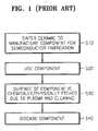
- FIG. 1is a flowchart of a conventional method of manufacturing ceramic components for semiconductor fabrication and processing them after using them.
- a ceramicis sintered to manufacture a component for semiconductor fabrication in step S 10 .
- the manufactured componentis used in step S 20 .
- a surface layer of the componentis chemically and/or physically etched due to plasma and cleaning in step S 30 .
- the componentis discarded.
- Such conventional ceramic components for semiconductor fabricationare manufactured using a sintering process, so it is difficult to control their surface characteristics except roughness.
- the surface of the ceramic componentsare chemically etched due to a radical and ion bombardment occurring in a reactor due to plasma, so the surface of the ceramic components erode and corrode. Accordingly, semiconductor fabrication progresses with the ceramic components having a different surface state than an initial surface state.
- the surface of a ceramic componentis continuously etched during reaction, the surface of the ceramic component changes and needs to be replaced with new expensive ceramic component.
- the present inventionprovides a method of fabricating and repairing ceramic components for semiconductor fabrication, through which erosion and polymer deposition occurring on ceramic components for semiconductor fabrication are decreased by modifying the dielectric surface of a component having an electrical insulation characteristic so that the ceramic components can be repaired after being used.
- a method of manufacturing and repairing a ceramic component for semiconductor fabricationincludes activating a surface layer of a component, which is manufactured by sintering a ceramic, and depositing a dielectric coating layer on the surface layer of the ceramic component using a plasma spray process; when the dielectric coating layer is damaged as the ceramic component is used for semiconductor fabrication, removing the dielectric coating layer; and repairing the ceramic component by depositing a dielectric coating layer on the surface layer of the ceramic component from which the damaged dielectric coating layer has been removed.
- the depositing the dielectric coating layerincludes depositing one material selected from the group consisting of alumina, zirconia, yttria, and YAG on the surface layer of the ceramic component.
- the repairing the ceramic componentincludes depositing one material selected from the group consisting of alumina, zirconia, yttria, and YAG on the surface layer of the ceramic component.
- the surface of a component for semiconductor fabricationis coated with alumina powder, yttria powder, YAG powder, or zirconia powder having excellent plasma and chemical resistance to a proper thickness to each semiconductor fabrication process, and the surface roughness and porosity of the coating can be controlled. Therefore, the present invention allows the surface of the component to be in a proper state to each semiconductor fabrication process, thereby reducing contamination due to particles and polymers. In addition, when the surface of the component is damaged, the expensive component for semiconductor fabrication can be repaired and reused by recoating the surface of the component, instead of discarding the component, thereby reducing cost of semiconductor fabrication.
- FIG. 1is a flowchart of a conventional method of manufacturing ceramic components for semiconductor fabrication and processing them after using them;
- FIG. 2is a flowchart of a method of manufacturing and repairing ceramic components for semiconductor fabrication using a plasma spray process according to an embodiment of the present invention
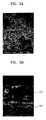
- FIG. 3Ashows the surface of a ceramic component manufactured for semiconductor fabrication according to the embodiment of the present invention.
- FIG. 3Bshows a cross-section of a ceramic component manufactured for semiconductor fabrication according to the embodiment of the present invention.
- FIG. 2is a flowchart of a method of manufacturing and repairing a ceramic component for semiconductor fabrication using a plasma spray process according to an embodiment of the present invention.
- the methodincludes activating a surface layer of a component for semiconductor fabrication, for example, an alumina component, which is manufactured by sintering a ceramic, and depositing a dielectric coating layer on the alumina surface layer using a plasma spray method in step S 100 and S 200 ; when the dielectric coating layer is etched and rugged as the ceramic component is used, removing the etched and rugged the dielectric coating layer in steps S 300 through S 500 ; and recoating the surface layer of the alumina component with a material having chemically and physically excellent characteristics to repair the ceramic component in step S 600 .
- a component for semiconductor fabricationfor example, an alumina component, which is manufactured by sintering a ceramic, and depositing a dielectric coating layer on the alumina surface layer using a plasma spray method in step S 100 and S 200 ; when the dielectric coating layer is etched
- a surface layer of a component for semiconductor fabricationwhich is manufactured by sintering a ceramic, is activated in step S 100 .
- a dielectric coating layeris formed by depositing a material, which has chemically and physically excellent characteristics and is suitable for semiconductor fabrication processes, on the activated surface layer of the alumina component using a plasma spray process in step 200 .
- the dielectric coating layercan be formed by coating the surface of the ceramic component with alumina, zirconia, yttria, or YAG.
- the density and porosity of a coating layercan be changed according to processing conditions, so a polymer generated as a byproduct during semiconductor fabrication can be removed from a reactor, and a ceramic material, density, and porosity suitable to the characteristics of each semiconductor fabrication process can be provided.
- the present inventionallows only the surface of a component to be controlled regardless of a base material of the component.
- the base materialmay be a ceramic, metal, plastic, or any other material.
- FIG. 3Ashows the surface of a ceramic component manufactured for semiconductor fabrication according to the embodiment of the present invention
- FIG. 3Bshows a cross-section of a ceramic component manufactured for semiconductor fabrication according to the embodiment of the present invention.
- reference numeral 101denotes a surface layer of an alumina substrate
- reference numeral 102denotes an yttrium oxide coating layer.
- the component with the dielectric coating layeris used for semiconductor fabrication in step S 300 .
- the dielectric coating layeris etched and rugged in step S 400 .
- the componentis discarded and replace with a new component, but according to the present invention, the component can be repaired and reused.
- the etched and rugged dielectric coating layeris removed using an etching process in step S 500 .
- the surface layer of the alumina substrateis recoated with a material, which has chemically and physically excellent characteristics and is suitable for semiconductor fabrication processes, so that the damaged component can be repaired.
- the damaged component for semiconductor fabricationcan be easily repaired by coating the surface layer of the alumina substrate with alumina, zirconia, yttria, or YAG, which has chemically and physically excellent characteristics.
- the present invention as described abovecan provide material and surface conditions suitable for the characteristics of each semiconductor fabrication process for a component for semiconductor fabrication, thereby securing reliability of semiconductor fabrication.
- a ceramic component for semiconductor fabricationcan be repaired and reused, so cost of semiconductor fabrication can be reduced.
Landscapes
- Engineering & Computer Science (AREA)
- Physics & Mathematics (AREA)
- Condensed Matter Physics & Semiconductors (AREA)
- General Physics & Mathematics (AREA)
- Manufacturing & Machinery (AREA)
- Computer Hardware Design (AREA)
- Microelectronics & Electronic Packaging (AREA)
- Power Engineering (AREA)
- Drying Of Semiconductors (AREA)
Abstract
Description
This application claims the priority of Korean Patent Application No. 2001-77411, filed Dec. 7, 2001, which is incorporated herein in its entirety by reference.
1. Field of the Invention
The present invention relates to a method of fabricating and repairing ceramic components for semiconductor fabrication, and more particularly, to a method of fabricating and repairing ceramic components for semiconductor fabrication, through which erosion and polymer deposition occurring on ceramic components for semiconductor fabrication are decreased by modifying the dielectric surface of a component having an electrical insulation characteristic so that the ceramic components can be repaired after being used.
2. Description of the Related Art
Usually, plasma is used for etching and deposition during semiconductor fabrication. Here, most of components used for semiconductor fabrication have a dielectric surface, and particularly they are alumina components formed using a sintering process.
During semiconductor fabrication, components having a dielectric surface exposed to plasma sustain damage such as erosion due to a chemical attack by a radical or physical attack due to ion bombardment caused by floating potential of plasma according to plasma conditions. When components are damaged due to erosion, particles occur on a semiconductor wafer due to alien substances, which badly affect a yield of semiconductor fabrication. Accordingly, when the dielectric surface of components is badly damaged due to, for example, erosion, it is necessary to replace the damaged components with new components.
In addition, a polymer generated as a byproduct during semiconductor fabrication must be smoothly attached to and detached from components for semiconductor fabrication according to process conditions. However, since the surface characteristics of components depend on processes of manufacturing the components, it is difficult to modify the surface characteristics except roughness, so it is difficult to control a state of surface of components to be suitable to semiconductor fabrication processes. In this case, components having new characteristics cannot be manufactured without changing the materials and manufacturing methods of all of components.
FIG. 1 is a flowchart of a conventional method of manufacturing ceramic components for semiconductor fabrication and processing them after using them. As shown in FIG. 1, a ceramic is sintered to manufacture a component for semiconductor fabrication in step S10. Next, the manufactured component is used in step S20. When the component is used, a surface layer of the component is chemically and/or physically etched due to plasma and cleaning in step S30. Then, the component is discarded.
Such conventional ceramic components for semiconductor fabrication are manufactured using a sintering process, so it is difficult to control their surface characteristics except roughness. In addition, when the conventional ceramic components are used, the surface of the ceramic components are chemically etched due to a radical and ion bombardment occurring in a reactor due to plasma, so the surface of the ceramic components erode and corrode. Accordingly, semiconductor fabrication progresses with the ceramic components having a different surface state than an initial surface state. Moreover, as the surface of a ceramic component is continuously etched during reaction, the surface of the ceramic component changes and needs to be replaced with new expensive ceramic component.
The present invention provides a method of fabricating and repairing ceramic components for semiconductor fabrication, through which erosion and polymer deposition occurring on ceramic components for semiconductor fabrication are decreased by modifying the dielectric surface of a component having an electrical insulation characteristic so that the ceramic components can be repaired after being used.
In one aspect of the present invention, there is provided a method of manufacturing and repairing a ceramic component for semiconductor fabrication. The method includes activating a surface layer of a component, which is manufactured by sintering a ceramic, and depositing a dielectric coating layer on the surface layer of the ceramic component using a plasma spray process; when the dielectric coating layer is damaged as the ceramic component is used for semiconductor fabrication, removing the dielectric coating layer; and repairing the ceramic component by depositing a dielectric coating layer on the surface layer of the ceramic component from which the damaged dielectric coating layer has been removed.
The depositing the dielectric coating layer includes depositing one material selected from the group consisting of alumina, zirconia, yttria, and YAG on the surface layer of the ceramic component. The repairing the ceramic component includes depositing one material selected from the group consisting of alumina, zirconia, yttria, and YAG on the surface layer of the ceramic component.
According to the present invention, the surface of a component for semiconductor fabrication is coated with alumina powder, yttria powder, YAG powder, or zirconia powder having excellent plasma and chemical resistance to a proper thickness to each semiconductor fabrication process, and the surface roughness and porosity of the coating can be controlled. Therefore, the present invention allows the surface of the component to be in a proper state to each semiconductor fabrication process, thereby reducing contamination due to particles and polymers. In addition, when the surface of the component is damaged, the expensive component for semiconductor fabrication can be repaired and reused by recoating the surface of the component, instead of discarding the component, thereby reducing cost of semiconductor fabrication.
The above features and advantages of the present invention will become more apparent by describing in detail a preferred embodiment thereof with reference to the attached drawings in which:
FIG. 1 is a flowchart of a conventional method of manufacturing ceramic components for semiconductor fabrication and processing them after using them;
FIG. 2 is a flowchart of a method of manufacturing and repairing ceramic components for semiconductor fabrication using a plasma spray process according to an embodiment of the present invention;
FIG. 3A shows the surface of a ceramic component manufactured for semiconductor fabrication according to the embodiment of the present invention; and
FIG. 3B shows a cross-section of a ceramic component manufactured for semiconductor fabrication according to the embodiment of the present invention.
Hereinafter, a preferred embodiment of the present invention will be described in detail with reference to the attached drawings.
FIG. 2 is a flowchart of a method of manufacturing and repairing a ceramic component for semiconductor fabrication using a plasma spray process according to an embodiment of the present invention. As shown in FIG. 2, the method includes activating a surface layer of a component for semiconductor fabrication, for example, an alumina component, which is manufactured by sintering a ceramic, and depositing a dielectric coating layer on the alumina surface layer using a plasma spray method in step S100 and S200; when the dielectric coating layer is etched and rugged as the ceramic component is used, removing the etched and rugged the dielectric coating layer in steps S300 through S500; and recoating the surface layer of the alumina component with a material having chemically and physically excellent characteristics to repair the ceramic component in step S600.
More specifically, in the method of manufacturing and repairing a ceramic component for semiconductor fabrication using a plasma spray process according to an embodiment of the present invention, a surface layer of a component for semiconductor fabrication, which is manufactured by sintering a ceramic, is activated in step S100.
Next, a dielectric coating layer is formed by depositing a material, which has chemically and physically excellent characteristics and is suitable for semiconductor fabrication processes, on the activated surface layer of the alumina component using a plasma spray process in step200. Here, the dielectric coating layer can be formed by coating the surface of the ceramic component with alumina, zirconia, yttria, or YAG. By forming the dielectric coating layer using alumina, zirconia, yttria, or YAG, cheaper and more reliable process conditions can be secured compare to a case of processing an entire ceramic component with yttria and YAG.
When the plasma spray process is used, the density and porosity of a coating layer can be changed according to processing conditions, so a polymer generated as a byproduct during semiconductor fabrication can be removed from a reactor, and a ceramic material, density, and porosity suitable to the characteristics of each semiconductor fabrication process can be provided. In other words, the present invention allows only the surface of a component to be controlled regardless of a base material of the component. The base material may be a ceramic, metal, plastic, or any other material.
FIG. 3A shows the surface of a ceramic component manufactured for semiconductor fabrication according to the embodiment of the present invention, and FIG. 3B shows a cross-section of a ceramic component manufactured for semiconductor fabrication according to the embodiment of the present invention. In FIG. 3B,reference numeral 101 denotes a surface layer of an alumina substrate, andreference numeral 102 denotes an yttrium oxide coating layer.
Thereafter, the component with the dielectric coating layer is used for semiconductor fabrication in step S300. As the component is used, the dielectric coating layer is etched and rugged in step S400. Conventionally, the component is discarded and replace with a new component, but according to the present invention, the component can be repaired and reused.
More specifically, the etched and rugged dielectric coating layer is removed using an etching process in step S500. Next, the surface layer of the alumina substrate is recoated with a material, which has chemically and physically excellent characteristics and is suitable for semiconductor fabrication processes, so that the damaged component can be repaired.
The damaged component for semiconductor fabrication can be easily repaired by coating the surface layer of the alumina substrate with alumina, zirconia, yttria, or YAG, which has chemically and physically excellent characteristics.
The present invention as described above can provide material and surface conditions suitable for the characteristics of each semiconductor fabrication process for a component for semiconductor fabrication, thereby securing reliability of semiconductor fabrication. In addition, in the course of or after use, a ceramic component for semiconductor fabrication can be repaired and reused, so cost of semiconductor fabrication can be reduced.
Claims (2)
1. A method of manufacturing and repairing a ceramic component for semiconductor fabrication, the method comprising:
activating a surface layer of a ceramic component, which is manufactured by sintering a ceramic, and depositing a dielectric coating layer on the surface layer of the ceramic component using a plasma spray process, wherein the step of depositing the dielectric coating layer on the surface layer of the ceramic component comprises depositing one material selected from the group consisting of alumina, zirconia, yttria, and YAG on the surface layer of the ceramic component;
when the dielectric coating layer is damaged as the ceramic component is used for semiconductor fabrication, removing the dielectric coating layer; and
repairing the ceramic component by depositing a dielectric coating layer on the surface layer of the ceramic component from which the damaged dielectric coating layer has been removed.
2. The method ofclaim 1 , wherein the repairing the ceramic component comprises depositing one material selected from the group consisting of alumina, zirconia, yttria, and YAG on the surface layer of the ceramic component.
Applications Claiming Priority (3)
| Application Number | Priority Date | Filing Date | Title |
|---|---|---|---|
| KR10-2001-0077411AKR100440500B1 (en) | 2001-12-07 | 2001-12-07 | Ceramic parts production and repair for semiconductor fabrication by plasma spray process |
| KR10-2001-0077411 | 2001-12-07 | ||
| KR2001-77411 | 2001-12-07 |
Publications (2)
| Publication Number | Publication Date |
|---|---|
| US20030129772A1 US20030129772A1 (en) | 2003-07-10 |
| US6833279B2true US6833279B2 (en) | 2004-12-21 |
Family
ID=19716777
Family Applications (1)
| Application Number | Title | Priority Date | Filing Date |
|---|---|---|---|
| US10/309,325Expired - LifetimeUS6833279B2 (en) | 2001-12-07 | 2002-12-04 | Method of fabricating and repairing ceramic components for semiconductor fabrication using plasma spray process |
Country Status (3)
| Country | Link |
|---|---|
| US (1) | US6833279B2 (en) |
| JP (1) | JP2003203906A (en) |
| KR (1) | KR100440500B1 (en) |
Cited By (16)
| Publication number | Priority date | Publication date | Assignee | Title |
|---|---|---|---|---|
| US20040063333A1 (en)* | 2002-09-30 | 2004-04-01 | Tokyo Electron Limited | Method and apparatus for an improved baffle plate in a plasma processing system |
| US20040081746A1 (en)* | 2000-12-12 | 2004-04-29 | Kosuke Imafuku | Method for regenerating container for plasma treatment, member inside container for plasma treatment, method for preparing member inside container for plasma treatment, and apparatus for plasma treatment |
| US20050147852A1 (en)* | 1999-12-10 | 2005-07-07 | Tocalo Co., Ltd. | Internal member for plasma-treating vessel and method of producing the same |
| US20050215059A1 (en)* | 2004-03-24 | 2005-09-29 | Davis Ian M | Process for producing semi-conductor coated substrate |
| US7137353B2 (en) | 2002-09-30 | 2006-11-21 | Tokyo Electron Limited | Method and apparatus for an improved deposition shield in a plasma processing system |
| US7147749B2 (en) | 2002-09-30 | 2006-12-12 | Tokyo Electron Limited | Method and apparatus for an improved upper electrode plate with deposition shield in a plasma processing system |
| US7163585B2 (en) | 2002-09-30 | 2007-01-16 | Tokyo Electron Limited | Method and apparatus for an improved optical window deposition shield in a plasma processing system |
| US7166200B2 (en) | 2002-09-30 | 2007-01-23 | Tokyo Electron Limited | Method and apparatus for an improved upper electrode plate in a plasma processing system |
| US7204912B2 (en) | 2002-09-30 | 2007-04-17 | Tokyo Electron Limited | Method and apparatus for an improved bellows shield in a plasma processing system |
| US7282112B2 (en) | 2002-09-30 | 2007-10-16 | Tokyo Electron Limited | Method and apparatus for an improved baffle plate in a plasma processing system |
| US7291566B2 (en) | 2003-03-31 | 2007-11-06 | Tokyo Electron Limited | Barrier layer for a processing element and a method of forming the same |
| US7552521B2 (en) | 2004-12-08 | 2009-06-30 | Tokyo Electron Limited | Method and apparatus for improved baffle plate |
| US7560376B2 (en) | 2003-03-31 | 2009-07-14 | Tokyo Electron Limited | Method for adjoining adjacent coatings on a processing element |
| US7601242B2 (en) | 2005-01-11 | 2009-10-13 | Tokyo Electron Limited | Plasma processing system and baffle assembly for use in plasma processing system |
| US7780786B2 (en) | 2002-11-28 | 2010-08-24 | Tokyo Electron Limited | Internal member of a plasma processing vessel |
| US7846291B2 (en) | 1999-12-10 | 2010-12-07 | Tokyo Electron Limited | Processing apparatus with a chamber having therein a high-corrosion-resistant sprayed film |
Families Citing this family (8)
| Publication number | Priority date | Publication date | Assignee | Title |
|---|---|---|---|---|
| US7052553B1 (en) | 2004-12-01 | 2006-05-30 | Lam Research Corporation | Wet cleaning of electrostatic chucks |
| US8074111B1 (en)* | 2006-09-18 | 2011-12-06 | Nortel Networks, Ltd. | System and method for responding to failure of a hardware locus at a communication installation |
| KR101171316B1 (en)* | 2010-04-06 | 2012-08-10 | (주)탑나노시스 | Method for repairing working stage with CNT antistatic treatment |
| US9212099B2 (en)* | 2012-02-22 | 2015-12-15 | Applied Materials, Inc. | Heat treated ceramic substrate having ceramic coating and heat treatment for coated ceramics |
| KR101581666B1 (en) | 2014-06-10 | 2015-12-31 | 한국세라믹기술원 | Recycling method of ceramic member using glass hard coating agent composition for recycling ceramic member |
| KR101965223B1 (en) | 2015-12-08 | 2019-04-03 | 한국세라믹기술원 | Regeneration method of ceramic member for recycle |
| KR101988223B1 (en) | 2016-06-29 | 2019-09-30 | 한국세라믹기술원 | Regeneration method of ceramic member for recycle using amorphous hard coating composition for recycling ceramic member |
| US20230223240A1 (en)* | 2020-06-25 | 2023-07-13 | Lam Research Corporation | Matched chemistry component body and coating for semiconductor processing chamber |
Citations (3)
| Publication number | Priority date | Publication date | Assignee | Title |
|---|---|---|---|---|
| US4412377A (en)* | 1981-01-23 | 1983-11-01 | Tokyo Shibaura Denki Kabushiki Kaisha | Method for manufacturing a hybrid integrated circuit device |
| US5900102A (en)* | 1996-12-11 | 1999-05-04 | General Electric Company | Method for repairing a thermal barrier coating |
| US6673709B2 (en)* | 2000-08-28 | 2004-01-06 | Snecma Moteurs | Formation of an aluminide coating, incorporating a reactive element, on a metal substrate |
Family Cites Families (5)
| Publication number | Priority date | Publication date | Assignee | Title |
|---|---|---|---|---|
| US3911891A (en)* | 1973-08-13 | 1975-10-14 | Robert D Dowell | Coating for metal surfaces and method for application |
| US4273824A (en)* | 1979-05-11 | 1981-06-16 | United Technologies Corporation | Ceramic faced structures and methods for manufacture thereof |
| WO1996012049A1 (en)* | 1994-10-14 | 1996-04-25 | Siemens Aktiengesellschaft | Protective layer for protecting parts against corrosion, oxidation and excessive thermal stresses, as well as process for producing the same |
| US6294261B1 (en)* | 1999-10-01 | 2001-09-25 | General Electric Company | Method for smoothing the surface of a protective coating |
| US6355356B1 (en)* | 1999-11-23 | 2002-03-12 | General Electric Company | Coating system for providing environmental protection to a metal substrate, and related processes |
- 2001
- 2001-12-07KRKR10-2001-0077411Apatent/KR100440500B1/ennot_activeExpired - Lifetime
- 2002
- 2002-12-04USUS10/309,325patent/US6833279B2/ennot_activeExpired - Lifetime
- 2002-12-05JPJP2002354144Apatent/JP2003203906A/enactivePending
Patent Citations (3)
| Publication number | Priority date | Publication date | Assignee | Title |
|---|---|---|---|---|
| US4412377A (en)* | 1981-01-23 | 1983-11-01 | Tokyo Shibaura Denki Kabushiki Kaisha | Method for manufacturing a hybrid integrated circuit device |
| US5900102A (en)* | 1996-12-11 | 1999-05-04 | General Electric Company | Method for repairing a thermal barrier coating |
| US6673709B2 (en)* | 2000-08-28 | 2004-01-06 | Snecma Moteurs | Formation of an aluminide coating, incorporating a reactive element, on a metal substrate |
Cited By (29)
| Publication number | Priority date | Publication date | Assignee | Title |
|---|---|---|---|---|
| US20080066647A1 (en)* | 1999-12-10 | 2008-03-20 | Tocalo Co., Ltd. | Internal member for plasma-treating vessel and method of producing the same |
| US20050147852A1 (en)* | 1999-12-10 | 2005-07-07 | Tocalo Co., Ltd. | Internal member for plasma-treating vessel and method of producing the same |
| US7879179B2 (en) | 1999-12-10 | 2011-02-01 | Tokyo Electron Limited | Processing apparatus with a chamber having therein a high-corrosion-resistant sprayed film |
| US7846291B2 (en) | 1999-12-10 | 2010-12-07 | Tokyo Electron Limited | Processing apparatus with a chamber having therein a high-corrosion-resistant sprayed film |
| US7364798B2 (en)* | 1999-12-10 | 2008-04-29 | Tocalo Co., Ltd. | Internal member for plasma-treating vessel and method of producing the same |
| US20040081746A1 (en)* | 2000-12-12 | 2004-04-29 | Kosuke Imafuku | Method for regenerating container for plasma treatment, member inside container for plasma treatment, method for preparing member inside container for plasma treatment, and apparatus for plasma treatment |
| US7811428B2 (en) | 2002-09-30 | 2010-10-12 | Tokyo Electron Limited | Method and apparatus for an improved optical window deposition shield in a plasma processing system |
| US7566368B2 (en) | 2002-09-30 | 2009-07-28 | Tokyo Electron Limited | Method and apparatus for an improved upper electrode plate in a plasma processing system |
| US7166166B2 (en) | 2002-09-30 | 2007-01-23 | Tokyo Electron Limited | Method and apparatus for an improved baffle plate in a plasma processing system |
| US7204912B2 (en) | 2002-09-30 | 2007-04-17 | Tokyo Electron Limited | Method and apparatus for an improved bellows shield in a plasma processing system |
| US7282112B2 (en) | 2002-09-30 | 2007-10-16 | Tokyo Electron Limited | Method and apparatus for an improved baffle plate in a plasma processing system |
| US8117986B2 (en) | 2002-09-30 | 2012-02-21 | Tokyo Electron Limited | Apparatus for an improved deposition shield in a plasma processing system |
| US7163585B2 (en) | 2002-09-30 | 2007-01-16 | Tokyo Electron Limited | Method and apparatus for an improved optical window deposition shield in a plasma processing system |
| US7147749B2 (en) | 2002-09-30 | 2006-12-12 | Tokyo Electron Limited | Method and apparatus for an improved upper electrode plate with deposition shield in a plasma processing system |
| US8118936B2 (en) | 2002-09-30 | 2012-02-21 | Tokyo Electron Limited | Method and apparatus for an improved baffle plate in a plasma processing system |
| US8057600B2 (en) | 2002-09-30 | 2011-11-15 | Tokyo Electron Limited | Method and apparatus for an improved baffle plate in a plasma processing system |
| US7566379B2 (en) | 2002-09-30 | 2009-07-28 | Tokyo Electron Limited | Method and apparatus for an improved upper electrode plate with deposition shield in a plasma processing system |
| US7166200B2 (en) | 2002-09-30 | 2007-01-23 | Tokyo Electron Limited | Method and apparatus for an improved upper electrode plate in a plasma processing system |
| US7137353B2 (en) | 2002-09-30 | 2006-11-21 | Tokyo Electron Limited | Method and apparatus for an improved deposition shield in a plasma processing system |
| US7678226B2 (en) | 2002-09-30 | 2010-03-16 | Tokyo Electron Limited | Method and apparatus for an improved bellows shield in a plasma processing system |
| US20040063333A1 (en)* | 2002-09-30 | 2004-04-01 | Tokyo Electron Limited | Method and apparatus for an improved baffle plate in a plasma processing system |
| US7780786B2 (en) | 2002-11-28 | 2010-08-24 | Tokyo Electron Limited | Internal member of a plasma processing vessel |
| US8449715B2 (en) | 2002-11-28 | 2013-05-28 | Tokyo Electron Limited | Internal member of a plasma processing vessel |
| US8877002B2 (en) | 2002-11-28 | 2014-11-04 | Tokyo Electron Limited | Internal member of a plasma processing vessel |
| US7560376B2 (en) | 2003-03-31 | 2009-07-14 | Tokyo Electron Limited | Method for adjoining adjacent coatings on a processing element |
| US7291566B2 (en) | 2003-03-31 | 2007-11-06 | Tokyo Electron Limited | Barrier layer for a processing element and a method of forming the same |
| US20050215059A1 (en)* | 2004-03-24 | 2005-09-29 | Davis Ian M | Process for producing semi-conductor coated substrate |
| US7552521B2 (en) | 2004-12-08 | 2009-06-30 | Tokyo Electron Limited | Method and apparatus for improved baffle plate |
| US7601242B2 (en) | 2005-01-11 | 2009-10-13 | Tokyo Electron Limited | Plasma processing system and baffle assembly for use in plasma processing system |
Also Published As
| Publication number | Publication date |
|---|---|
| JP2003203906A (en) | 2003-07-18 |
| US20030129772A1 (en) | 2003-07-10 |
| KR20030047036A (en) | 2003-06-18 |
| KR100440500B1 (en) | 2004-07-15 |
Similar Documents
| Publication | Publication Date | Title |
|---|---|---|
| US6833279B2 (en) | Method of fabricating and repairing ceramic components for semiconductor fabrication using plasma spray process | |
| US9184060B1 (en) | Plated metal hard mask for vertical NAND hole etch | |
| TWI414634B (en) | Extending lifetime of yttrium oxide as a plasma chamber material | |
| CN108884546B (en) | Coated semiconductor processing component with resistance to chlorine and fluorine plasma erosion and composite oxide coating thereof | |
| CN102210196B (en) | Plasma resistant coatings for plasma chamber components | |
| CN113614900B (en) | Ceramic nozzle with conductive electrode | |
| JP5578383B2 (en) | Plasma resistant material | |
| US20030019579A1 (en) | Dry etching apparatus for manufacturing semiconductor devices | |
| KR20100052502A (en) | Method of coating semiconductor processing apparatus with protective yttrium-containing coatings | |
| US20160079040A1 (en) | Plasma Processing Devices Having a Surface Protection Layer | |
| EP2119806A1 (en) | Multilayer film forming method and multilayer film forming apparatus | |
| KR20150068285A (en) | Parts of semiconductor and display equipments with improved anti-plasma corrosion and method improving anti-plasma corrosion of parts | |
| US20040144319A1 (en) | Plasma treatment container internal member, and plasma treatment device having the plasma treatment container internal member | |
| CN1227668A (en) | Method and apparatus for etching a semiconductor wafer | |
| WO1999063571A1 (en) | Pedestal insulator for a pre-clean chamber | |
| Bale et al. | Deep plasma etching of piezoelectric PZT with SF 6 | |
| KR100454987B1 (en) | Yttria Coated parts production and repair for semiconductor fabrication by plasma spray process | |
| KR102831967B1 (en) | Large-sized sintered yttrium oxide | |
| JP6358492B2 (en) | Plasma resistant material | |
| KR102517083B1 (en) | Coating surface treatment method to improve the elapsed time of semiconductor etch process equipment | |
| JP5350174B2 (en) | Plasma etching method | |
| CN113808935B (en) | Corrosion-resistant coating forming method and device, plasma component and reaction device | |
| JPH05160078A (en) | Dry etching method | |
| KR101574250B1 (en) | Method of fabricating Micropatterns of Platinum Thin Films by Fluoride-Based Inductively Coupled Plasma Eching | |
| KR100789618B1 (en) | How to remove polymer from chamber |
Legal Events
| Date | Code | Title | Description |
|---|---|---|---|
| AS | Assignment | Owner name:KOMICO CO., LTD., KOREA, REPUBLIC OF Free format text:ASSIGNMENT OF ASSIGNORS INTEREST;ASSIGNOR:CHOI, JIN-SIK;REEL/FRAME:013865/0314 Effective date:20021205 | |
| STCF | Information on status: patent grant | Free format text:PATENTED CASE | |
| FPAY | Fee payment | Year of fee payment:4 | |
| FPAY | Fee payment | Year of fee payment:8 | |
| AS | Assignment | Owner name:MICO. LTD., KOREA, REPUBLIC OF Free format text:CHANGE OF NAME;ASSIGNOR:KOMICO CO., LTD.;REEL/FRAME:033783/0663 Effective date:20130708 | |
| AS | Assignment | Owner name:KOMICO LTD., KOREA, REPUBLIC OF Free format text:ASSIGNMENT OF ASSIGNORS INTEREST;ASSIGNOR:MICO. LTD.;REEL/FRAME:033818/0406 Effective date:20130830 | |
| FPAY | Fee payment | Year of fee payment:12 |