US6833031B2 - Method and device for coating a substrate - Google Patents
Method and device for coating a substrateDownload PDFInfo
- Publication number
- US6833031B2 US6833031B2US09/812,075US81207501AUS6833031B2US 6833031 B2US6833031 B2US 6833031B2US 81207501 AUS81207501 AUS 81207501AUS 6833031 B2US6833031 B2US 6833031B2
- Authority
- US
- United States
- Prior art keywords
- substrate
- assembly
- metallization
- station
- line apparatus
- Prior art date
- Legal status (The legal status is an assumption and is not a legal conclusion. Google has not performed a legal analysis and makes no representation as to the accuracy of the status listed.)
- Expired - Fee Related, expires
Links
Images


Classifications
- C—CHEMISTRY; METALLURGY
- C23—COATING METALLIC MATERIAL; COATING MATERIAL WITH METALLIC MATERIAL; CHEMICAL SURFACE TREATMENT; DIFFUSION TREATMENT OF METALLIC MATERIAL; COATING BY VACUUM EVAPORATION, BY SPUTTERING, BY ION IMPLANTATION OR BY CHEMICAL VAPOUR DEPOSITION, IN GENERAL; INHIBITING CORROSION OF METALLIC MATERIAL OR INCRUSTATION IN GENERAL
- C23C—COATING METALLIC MATERIAL; COATING MATERIAL WITH METALLIC MATERIAL; SURFACE TREATMENT OF METALLIC MATERIAL BY DIFFUSION INTO THE SURFACE, BY CHEMICAL CONVERSION OR SUBSTITUTION; COATING BY VACUUM EVAPORATION, BY SPUTTERING, BY ION IMPLANTATION OR BY CHEMICAL VAPOUR DEPOSITION, IN GENERAL
- C23C14/00—Coating by vacuum evaporation, by sputtering or by ion implantation of the coating forming material
- C23C14/22—Coating by vacuum evaporation, by sputtering or by ion implantation of the coating forming material characterised by the process of coating
- C23C14/56—Apparatus specially adapted for continuous coating; Arrangements for maintaining the vacuum, e.g. vacuum locks
Definitions
- the present inventionrelates generally to methods and systems for coating a substrate. More particularly, the present invention relates to methods and devices for depositing a metal layer onto a thermoform that is of a sufficient thickness for shielding of electromagnetic interference (“EMI”) and radiofequency interference (“RFI”).
- EMIelectromagnetic interference
- RFIDradiofequency interference
- U.S. Pat. No. 5,811,050 to Gabowerwhich is incorporated herein by reference, has proposed depositing a thin layer of metal onto a thermoform to create a protective barrier for EMI and RFI.
- One method for depositing the metal layer onto the thermoformis a batch mode process.
- a first step of the methodincludes thermoforming (i.e. shaping) the thermoform substrate.
- the shaped thermoformsare then placed into the vacuum chamber and a vacuum source is used to create a vacuum in the chamber.
- a source of metalis vaporized and deposited onto the thermoform substrate.
- the batch processesis slow, time consuming, and impurities can be introduced into the metallized object during transport into and out of the vacuum chamber.
- one specific problem with the batch processis the creation of the vacuum environment in the deposition chamber. Because the vacuum chamber usually has a large volume (typically about 300,000 in 3 ), the creation of the vacuum environment takes a long period of time to create.
- Another problem of batch processingis that the thermoform must be separately shaped and cut from the thermoform sheet and it is often necessary to manually handle the thermoformed substrate, both prior and subsequent to the coating process. Care must be taken in such handling steps to avoid contamination or introduction of impurities which may lead to imperfections in the metal layer and leakage in the EMI/RFI shield.
- U.S. Pat. No. 5,908,506provides a continuous vapor deposition apparatus that appears to have stationary process chambers.
- U.S. Pat. No. 5,811,050describes an apparatus for vacuum depositing a metallic coating on thermoformed blanks that are placed on a carrier that revolves around a stationary tungsten filament.
- U.S. Pat. No. 5,076,203recites passing a web over spools past a stationary source of metal and an electron beam heater.
- U.S. Pat. No. 4,261,808describes a vertical vacuum coating apparatus that deposits a metal layer onto a moving substrate with a fixed cathode system.
- the present inventionprovides improved methods and systems for depositing a coating material onto a substrate.
- the methods and systemsare used for vacuum metallizing a thermoform or other substrate for creating an EMI/RFI shield.
- the systems of the present inventiongenerally have at least one processing apparatus that is movable orthogonal to a plane of the substrate.
- the processing apparatuscan be moved adjacent the substrate or to contact the substrate, a platform, and/or a second processing apparatus to process the substrate.
- the processing apparatuseshave a small volume cavity in which a vacuum can be created for the delivery of a vaporized metal or other coating material.
- the small vacuum cavities of the processing apparatuses of the present inventionallow a vacuum source to create a vacuum environment in a shorter amount of time than conventional vacuum chambers, thus improving the speed of manufacturing of the substrates.
- the cavities of the processing apparatusescan house a shaping assembly, a pre-treatment assembly (e.g. glow discharge), a metallizing assembly (e.g. vacuum metallization, arc plasma deposition, ion deposition), heating elements, a cutting assembly or the like.
- the systems of the present inventionare configured as in-line system that has a plurality of movable processing apparatuses.
- the in-line systems of the present inventionallow for the processing of spools or rolls of a substrate, such as a thermoform, such that no manual handling of the thermoform is required in intermediate steps.
- the processing apparatusescan be configured to thermoform, pre-treat the substrate, metallize and/or cut the thermoform using the single in-line system.
- the substratemay enter into the processing area either as a structural form which has been subject to prior processing (referred to as thermoforming) or the substrate may enter the processing area as a flat substrate and be subject to thermoforming followed by metallization, or alternatively vacuum metallization followed by thermoforming.
- the systems of the present inventioninclude a series of movable processing apparatuses on one or both sides of the substrate.
- the assembliescan all be adapted to perform the same function (e.g. metallize) or each of the processing apparatuses can perform different functions (e.g., thermoform, metallize and cut).
- the substratecan be moved to a first processing apparatus for shaping (e.g., thermoforming) of the substrate.
- the shaped substratecan be then be moved to a second processing apparatus which can deposit a metal layer onto the shaped substrate (e.g., vacuum metallization). Finally, the shaped and metallized substrate can be transported to a third processing apparatus that can cut the shaped and metallized form out of the substrate. It should be appreciated that additional processing apparatuses can also be incorporated into the previous example, such as surface treatment apparatuses, heating apparatuses, or the like.
- the processing apparatuses of the present inventioncan include one or more modular units for providing multiple interfaces for processing the substrate.
- Such processing apparatuseswill be movable orthogonal to the plane of the substrate and rotatable so that a desired processing interface of the modular units can be moved into position to process the substrate.
- Such a configurationallows for a multitude of processes to be accomplished either on a single sheet of material or as a part of a continuous inline process in which a polymer or flexible film is unrolled and processed from beginning to end.
- each processing apparatusincludes at least three modular units, and preferably between three and six modular units.
- Each modular unit of each processing apparatuscan have the same or different functions.
- each of the modular unitswill have the same modular unit, for example a metallization unit.
- the metallization unitwill be used deposit a metal layer onto the substrate. Once the metal source has been depleted in the metallization unit, the processing apparatus can be rotated and a metallization unit having a full metal source can be used. Once the depleted metal source has been rotated away, the metal source can be manually or mechanically replaced.
- Such a configurationlimits the “down time” of the system and improves the output and production of the system.
- each of the modular units of the processing apparatuscan have a different functional modular unit.
- a first modular unitcan be used to heat the thermoform.
- the first modular unitcan be rotated away and a second shaping modular unit can process and shape the substrate.
- the next modular unitssuch as a surface treatment assembly, metallization assembly, and cutting assembly modular unit can be rotated towards the substrate to process the substrate.
- the rotatable, modular processing apparatusesallow for multiple or complete processing of the substrate while maintaining the position of a substrate in a single position. Such systems can reduce the footprint of the system on the manufacturing floor.
- the present inventioncan create EMI/RFI shields that can be used within electronic devices and products to reduce the amount of electromagnetic radiation that is emitted from and enters the electronic device.
- the EMI RFI shields enabled by the equipment described aboveare based upon the application of a relatively stable and uniform layer of aluminum on a polymer substrate.
- the present inventioncan apply any number of different metal layers (e.g., silver, copper, gold, nickel, or the like) to any number of substrate materials (e.g., polycarbonate, ABS, PVC, or the like) through a variety of metallization processes.
- the present inventionprovides an apparatus for coating a substrate.
- the apparatuscomprises a support that supports the substrate and at least one movable processing apparatus that can deposit a metal layer onto the substrate.
- the processing apparatusis movable between a first position adjacent the substrate and a second position apart from the substrate.
- the present inventionprovides an apparatus for metallizing a substrate.
- the apparatuscomprises a support that can maintain at least a portion of the substrate along a first plane and at least one rotatable processing apparatus that is movable substantially orthogonal to the orientation of the substrate.
- the processing apparatuscomprises a plurality of modular units that includes at least one of a thermoform assembly, a heating assembly, a metallizing assembly, or a cutting assembly.
- the present inventionprovides an in-line apparatus for creating an EMI shield
- the apparatuscomprises a conveyor assembly that moves a substrate from a first position to a second position and a movable shaping chamber disposed at the first position to shape the substrate.
- a metallization chambercan create a seal around the shaped substrate and can deposit a metal layer onto the shaped substrate, and a cutting assembly disposed at the second position to cut the shaped substrate, the cutting assembly being movable relative to the shaped substrate.
- the present inventionprovides a method of manufacturing an EMI shield.
- the methodcomprises positioning a substrate on a support.
- a processing apparatusis moved adjacent to the substrate, a metal layer is deposited on the substrate and the processing apparatus is moved away from the substrate.
- FIG. 1is a simplified cross sectional view of a processing apparatus of the present invention
- FIG. 2is a cross sectional view of a simplified exemplary processing apparatus of the present invention
- FIG. 3is a simplified view of a system comprising a plurality of processing apparatuses in which the processing apparatuses are disposed on both sides of a substrate;
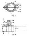
- FIG. 4is a partial cross sectional view of a first and second processing apparatus
- FIG. 5is a simplified top view of a system of the present invention.
- FIG. 6is an end view of an upper and lower processing apparatus
- FIGS. 7A and 7Bare end views of a single removable, modular unit of the processing apparatus
- FIG. 8Ais a top view illustrating the cavity of the modular unit of FIGS. 7A and 7B;
- FIG. 8Bis a cross sectional view along line A—A of FIG. 8A;
- FIG. 9is an end view of two attached modular units of the processing apparatus.
- FIG. 10Ais a top view of a modular unit comprising heating elements
- FIG. 10Bis a cross-sectional end view of a modular unit comprising heating elements
- FIG. 11Ais a top view of a modular unit comprising a conditioning assembly
- FIG. 11Bis a cross sectional end view of a modular unit comprising a conditioning assembly
- FIG. 12Ais a top view of a modular assembly comprising a plurality of filaments and canes;
- FIG. 12Bis a cross-sectional end view of a modular unit comprising a plurality of filaments and canes;
- FIG. 13is a close-up view of a metal cane and a filament
- FIG. 14is a close-up view of another embodiment of a metal cane and a filament
- FIG. 15is a top view of a shaped substrate within the processing zone of the modular unit
- FIG. 16is a cross-sectional end view illustrating a modular unit comprising a steel-rule die.
- FIG. 17is a schematic view of a processing system of the present invention.
- the present inventionprovides improved systems and methods for depositing a metal layer onto a shaped polymer substrate.
- the systems of the present inventionrely on the use of at least one movable processing apparatus to treat a substrate. Treatments can include surface treatment, preheating, shaping, depositing a metal layer, cutting, or the like.
- the methods and systems of the present inventionare for use in producing EMI/RFI shields for electronic devices.
- the final EMI/RFI shieldsare composed of a metallized thermoform that are manufactured with the processes and systems of the present invention.
- the systems of the present inventioninclude at least one movable processing apparatus, and typically a first processing apparatus disposed on a first side of the substrate and a second processing apparatus disposed on a second side of the substrate.
- the first processing apparatuscan include a mold while the second side can include a corresponding mold to shape the substrate.
- both the first and second processing apparatuscan be used so as to metallize both sides of the substrate.
- the apparatuses of the present inventioncan be adapted to perform only a single process of the processing of the substrate.
- the apparatuses of the present inventioncan be used to only metallize flat substrates.
- the apparatuses of the present inventioncan be used to only shape (e.g., thermoform) the substrate.
- the apparatusdoes not have to be an in-line process, but instead the processing apparatus can be a stand alone device that allows a user to manually position the substrate in a processing position.
- the methods and systems of the present inventioncan also extend to depositing a coating on any type of substrate.
- one exemplary system 10 of the present inventionincludes a housing 11 having a support 12 that can position a substrate 14 adjacent at least one processing apparatus 16 .
- the processing apparatusis movable relative to the substrate 14 and will typically be movable orthogonal from the substrate 14 when the substrate is positioned on the support 12 (i.e. up/down in the case of a vertical application or forward/back in the case of a horizontal application.).
- each of the processing apparatus 16typically includes a body 18 that defines a cavity 20 .
- the bodytypically has at least one conduit 22 for delivering a gas, creating a vacuum, delivering electrical energy to the cavity, or the like.
- some processing apparatusescan contact the support 12 , the substrate 14 and/or a platform 24 (FIG. 1) to provide a seal around the target portion of the substrate 14 .
- a vacuumcan be created around the target portion of the substrate 14 prior to a delivery of a metal onto the substrate.
- the cavity 20typically will have a volume of approximately 16,000 in 3 . In contrast, standard vacuum chambers will have a total volume of almost 300,000 in 3 .
- the cavityhas a smaller volume than conventional vacuum chambers, a vacuum can be created quicker and the processing of the substrate can be completed faster. It should be appreciated however, that the size of the body 18 and cavity 20 can be varied to allow for different sized substrates and different processing speeds. Additionally, not all processes of the present invention require a creation of a vacuum. For example, if the processing apparatus 16 is used to shape the substrate the body 18 , the processing apparatus may not have a cavity and a vacuum may not be created around the substrate.
- FIG. 3illustrates another embodiment of the system of the present invention.
- the system 10can includes a plurality of stations for treating the substrate 14 .
- the system 10can include a shaping station 26 , a metallization station 28 , and a cutting station 30 .
- a conveyor support 32can be incorporated into the system to transport the substrate 14 from station to station.
- any number of stationscan be provided, and the stations can be positioned in any order desired.
- each of the stationscan be configured to deposit a metal layer onto the substrate 14 . Because each of the vacuum cavities has a smaller volume than conventional vacuum chambers, a vacuum can be created around the substrate quicker than conventional vacuum chambers and the entire substrate can be metallized in a shorter period of time.
- exemplary stationsinclude a first unit 16 positioned on a first side 32 of the substrate and a second unit 16 ′ positioned on a second side 34 of the substrate.
- the units 16 , 16 ′will work in tandem to process the substrate so that when the units are moved adjacent the substrate, each of the units can simultaneously process both sides of the substrate.
- the first unit 16 and second unit 16 ′can have complimentary sides of a mold for shaping the substrate.
- the first and second unitswill press the substrate to shape the substrate.
- the first and second unitscan employ a heating element, a vacuum and/or air pressure to facilitate forming of the substrate (not shown).
- the next stationcan be used to deposit the metal layer onto the shaped substrate 14 .
- the first and second unitscan contact the body 18 , the substrate 14 , and/or each other with contact points 35 to create a vacuum around the shaped substrate.
- the contact pointscan include aligned protrusions and detents to create additional pressure on the substrate to prevent the leakage of air into the chamber.
- a vacuum source(not shown) can create a vacuum in the cavity 20 and the metal layer can be deposited on one or two sides of the shaped substrate.
- the shaped and metallized substratecan be transported to the third station where the shaped substrate will be at least partially cut away from the remaining portion of the substrate with the first and second units.
- the first and second unitscan include a cutting assembly (not shown) that contacts the substrate to cut the shaped portion of the substrate off of the remainder of the substrate.
- FIG. 5illustrates one representative system 10 of the present invention.
- the substrate 14is shown as a film roll moving from left to right and between the first and second units 16 .
- the first and second unitsare connectable to a movable end unit 36 that provides an interface with fixed equipment.
- the end unit 36can be connected to a source of electrical power 40 , a gas unit 42 which houses various types of gases used in processing of the substrate, a vacuum unit 44 which contains various types of pumps, blowers, valves, or the like, necessary to effect and release vacuum and sources 46 of other types of processing materials like liquids or gases used to create positive pressure for some thermoforming operations.
- the connections between the various unitsare accomplished with suitably designed and conventional mechanical quick connect/disconnect fittings and movable hoses and cables.
- the systems of the present inventiongenerally include a computer control system (not shown) to control the movement of the processing apparatuses, the end unit, the substrates, and the like.
- FIG. 6 to FIG. 19Exemplary rotatable processing apparatuses of the present invention are illustrated in FIG. 6 to FIG. 19 .
- the processing apparatuses 16can include a plurality of modular units 50 such that rotation of the processing apparatuses 16 allows a different modular unit to be moved adjacent or into contact with the substrate. Such an assembly allows the processing apparatus to perform a different process (or the same process) to the substrate 14 using only a single processing apparatus.
- the substrate 14can be positioned between the first and second apparatuses 16 , 16 ′ in a direction substantially parallel to both a first unit centerline 52 and second unit centerline 54 .
- the substrate 14is typically composed of a nominally planar layer of material such as a metal, polymer, ceramic, or the like.
- the first and second unit 16 , 16 ′can rotate clockwise or counterclockwise independently of one another and can also move in a direction that is orthogonal to the substrate plane. Movement of the first and second processing units towards the substrate by the first and second units 16 , 16 ′ leads to contact with the substrate and the creation of an isolated area on the substrate where various processes can be performed on the substrate.
- Each of the first and second processing apparatuses 16 , 16 ′can include a plurality of nominally independent modular units 50 .
- FIGS. 7A and 7Bshow one specific embodiment of the present invention in which each modular unit 50 is a detachable unit having a triangular cross section.
- Each modular unit 50can be coupled to the remaining assembled modular units so as to form a complete processing unit 16 .
- the most extreme surface from a center of rotation 58is a processing plane 60 .
- the processing plancan contain an opening to the interior cavity 20 of the single modular unit for purposes of performing various types of mechanical, electrical, and thermal processing, as will be explained in more detail below.
- the triangular modular units 50can be coupled to a frame (not shown) of the processing unit 16 .
- FIGS. 8A and 8Bshow one embodiment of an individual modular unit that contains a processing cavity 20 .
- the body 18 surrounding the cavityis of size, strength, and thickness as required to perform a particular process.
- the surface 60 of the modular unittypically comes in contact with the substrate 14 .
- the surfaceis typically used to form a seal with substrate 14 .
- the sealmay only establish nominal contact so as to hold the substrate mechanically or the seal may be have a tighter contact, for example with a detent and protrusion (not shown) so as to enable the creation of a vacuum between the substrate 14 and the cavity 20 .
- the surface 60can contact the support 12 , a platform 24 or another surface of a second processing apparatus.
- FIG. 9shows a side view of two single modular units 50 , 50 ′ that are attached via simple mechanical means, in this case, a cap head bolt 62 positioned and size in such a manner so as to not impose itself on an adjacent single modular units.
- the sides of the modular units 50may also contain grooves or other mechanical means to achieve a tight and structural attachment of adjacent modular units to form a process assembly 16 .
- the modular units 50 of the present inventioncan include a variety of treatment assemblies.
- the modular unitcan include a thermal assembly 64 .
- the thermal assemblyis used to create and deliver heat via convection to one or both sides of the substrate.
- the thermal assembly 64can deliver heat through cavity or chamber 20 with one or more heating elements 66 (such as a resistive metal filament) that are connected to an electrical circuit and energy source via a conduit 68 . While resistive filaments are illustrated, it should be appreciated that various other conventional or proprietary heating assemblies can be used in the modular units of the present invention. For example, in some processes, by creating a vacuum, heat may be applied purely through radiation.
- FIGS. 11A and 11Billustrate a pre-conditioning assembly 70 that can be used with the modular unit 50 to create a more favorable environment for a subsequent treatments of the substrate.
- a glow discharge processis depicted in which a gas dispersal mechanism 72 is placed within the cavity 20 and a source of gas (nitrogen, argon, etc.) is provided via an access hole and conduit 74 that is connected to the source of gas (not shown).
- a source of gasnitrogen, argon, etc.
- FIGS. 11A and 11Billustrate a pre-conditioning assembly 70 that can be used with the modular unit 50 to create a more favorable environment for a subsequent treatments of the substrate.
- a glow discharge processis depicted in which a gas dispersal mechanism 72 is placed within the cavity 20 and a source of gas (nitrogen, argon, etc.) is provided via an access hole and conduit 74 that is connected to the source of gas (not shown).
- a pre-conditioning assemblythat precedes a vacuum metallization process and other
- FIGS. 12A and 12Billustrates a metallization assembly 76 used for depositing a metal layer onto the substrate. It should be appreciated that the preconditioning assembly 70 of FIG. 11A and 11B would be contained in the view of FIGS. 12A and 12B, but are omitted for clarity.
- tungsten filaments 78in various shapes but often of the form of a spring-like spiral with an interior opening sufficient for the placement of L-shaped “canes” 80 are placed around and within the cavity. The tungsten filaments are connected to a source of electrical energy via a conduit 82 .
- a vacuumis created within the cavity using a number of ports 81 that are connected to vacuum source (not shown) having an external array of pumps, blowers, and various other mechanical means for creating a vacuum.
- the filaments 78 and canes 80can either be manually placed into the cavity or automated equipment can be used to place the filaments 78 and canes 80 in the metallization assembly 76 .
- FIGS. 13 and 14Two specific arrangements of the canes 80 and filaments 78 are illustrated in FIGS. 13 and 14.
- the assembly of a metal canes 80 and a tungsten filament 78are placed into the electrical and mechanical interface 82 much like pushing or screwing a light bulb into its socket (FIG. 13 ).
- the electrical and mechanical interface 82includes a conductive interior designed with sufficient mechanical tolerances to allow the tungsten filament 78 to snugly fit and remain in place while at the same time establishing an electrical connection to the power source.
- the assembly of tungsten filament and metal canecan be placed by hand from time to time as required or it may be placed by any number of automated methods.
- a long “bar”(not shown) may be pre-assembled in which at regular distances the filament/cane combination is attached to an electrically conductive bar which is, in turn, is mechanical/electrically attached to certain points of the modular unit 50 so as to establish a path for electricity to charge the bar.
- combination of filament 78 and cane 80can take any number of geometric configurations in order to properly vaporize and distribute the metal cane.
- the tungsten filament 78may be a hollow cylinder 84 that is connected to the mechanical/electrical interface 82 by simply pushing it into a slightly larger cylindrical opening in the modular unit.
- the canecan be in the shape of a cylinder 86 that is simply pushed into the cylindrical tungsten insert 84 .
- the tungsten insert 84 or any other tungsten filament configurationmay be replaced with any suitable material that provides for the rapid generation of heat (via resistance) while retaining mechanical properties necessary for vacuum metallization.
- FIG. 15is a top view of a process surface 60 and a shaped substrate 14 located within a process zone and containing an area intended to be cut out (AKA the “part” 88 ).
- the processcan use a mechanical cutting element 90 (e.g., a steel ruled die, or the like) that comes in contact with the substrate 14 and is designed to penetrate the polymer substrate.
- the cutting element 90can be attached to the sides of the modular unit 50 via various mechanical means 92 .
- the cutting edge 94in this case, would exceed the plane 60 of the substrate by an amount necessary to achieve cutting.
- a corresponding modular unit of the other first or second unit 16 ′can provide a bearing surface for the cutting edge 94 or an additional cutting element 90 to improve the cutting process.
- Each of the modular units 50will include a number of conduits and ports for coupling the assemblies 64 , 72 , 76 , 90 to their respective sources (e.g. power source, gas source, vacuum source, or the like).
- FIG. 17shows a modular unit 50 that has an internal conduits 96 for drawing vacuum, transporting electrical energy, transporting gas, or the like. These internal conduits connect the cavity 20 of the individual modular units 50 to a movable end unit 36 which has corresponding conduits 97 that are connectable to connectors, power supplies, pumps and blowers, etc. needed to provide electricity provide vacuum capabilities, and provide various gases for processing.
- Various types of connectors considered standard in the mechanical equipment industryprovide the connection between the end unit 36 and modular process units 50 .
- the end unit 36is typically moved laterally with respect to the processing apparatus 16 in order to effect a connection (or disengage a connection) with the conduit 96 of the modular unit 50 .
- This movementis computer controlled to be coordinated with the rotational and linear movement of the processing apparatus 16 such that at the start of a sequence the conduits of the processing apparatuses 16 , 16 ′ are aligned the end unit 36 . If the processing apparatuses are to be rotated, the end unit 36 can move away from the processing apparatus 16 and disengage its various connections. The upper/lower apparatuses are then raised away from the substrate a sufficient distance to allow the rotation of the processing apparatus to position the new processing unit to become oriented directly above or below the substrate.
- the substratecan then be moved if a part of an inline continuous process, removed in the case of a sheet process or allowed to stay in place for the next process.
- the first and second units 16 , 16 ′are then lowered and raised to come in contact with the substrate.
- the end unit 36can then be re-engaged with the first and second units 16 , 16 ′ to connect the conduit 96 to the desired source.
- thermoformcan be automatically or manually roll-fed or sheet-fed into the processing apparatuses of the present invention.
- a first stationis typically a shaping or thermoforming station. Thermoforming is the heating and molding of plastic substrate into a shaped product. The shaped product can take a variety of forms to create an EMI shield.
- Various EMI shieldsare described and illustrated in U.S. Pat. No. 5,811,050 and patent application Ser. Nos. 09/788,263, filed Feb.
- the shaping processing apparatus 26can use either a vacuum to pull the polymer sheet into the shape of the mold and/or air pressure to force the polymer sheet into the shape of the mold.
- the present inventioncan use matched male/female molds (with or without the vacuum and air pressure) to facilitate the molding of the polymer.
- the thermoforming assemblies 16can use a variety of heating elements to soften the substrate 14 , such as ceramic, quartz tubes, lamps, coils, or the like. In use, the thermoforming assembly 26 is moved to contact the polymer substrate 14 . The substrate can be heated to the desired softness or “sag” and can then be formed in the mold on the first and second units.
- a vacuumcan be coupled to one of the first and second modules and a pressure source can be coupled to the other of the first and second modules.
- the shaped substratecan then be transported either manually or with a conveyor system 32 to the metallization assembly 28 .
- the metallization assembly 28can create a vacuum around the desired portion of the substrate and the metal layer can be deposited onto the shaped substrate. Thereafter, the metallized substrate can be moved to the cutting assembly 30 for final processing of the substrate (FIGS. 15 and 16 ). While not shown, it should be appreciated that a variety of pre-conditioning assemblies 64 and other finishing assemblies can be used to prep and finish the resulting EMI shield.
Landscapes
- Chemical & Material Sciences (AREA)
- Chemical Kinetics & Catalysis (AREA)
- Engineering & Computer Science (AREA)
- Materials Engineering (AREA)
- Mechanical Engineering (AREA)
- Metallurgy (AREA)
- Organic Chemistry (AREA)
- Shielding Devices Or Components To Electric Or Magnetic Fields (AREA)
- Physical Vapour Deposition (AREA)
Abstract
Description
Claims (23)
Priority Applications (2)
| Application Number | Priority Date | Filing Date | Title |
|---|---|---|---|
| US09/812,075US6833031B2 (en) | 2000-03-21 | 2001-03-19 | Method and device for coating a substrate |
| US11/010,559US20050202174A1 (en) | 2000-03-21 | 2004-12-13 | Method and device for coating a substrate |
Applications Claiming Priority (3)
| Application Number | Priority Date | Filing Date | Title |
|---|---|---|---|
| US19092000P | 2000-03-21 | 2000-03-21 | |
| US19877700P | 2000-04-21 | 2000-04-21 | |
| US09/812,075US6833031B2 (en) | 2000-03-21 | 2001-03-19 | Method and device for coating a substrate |
Related Child Applications (1)
| Application Number | Title | Priority Date | Filing Date |
|---|---|---|---|
| US11/010,559DivisionUS20050202174A1 (en) | 2000-03-21 | 2004-12-13 | Method and device for coating a substrate |
Publications (2)
| Publication Number | Publication Date |
|---|---|
| US20020002945A1 US20020002945A1 (en) | 2002-01-10 |
| US6833031B2true US6833031B2 (en) | 2004-12-21 |
Family
ID=26886569
Family Applications (2)
| Application Number | Title | Priority Date | Filing Date |
|---|---|---|---|
| US09/812,075Expired - Fee RelatedUS6833031B2 (en) | 2000-03-21 | 2001-03-19 | Method and device for coating a substrate |
| US11/010,559AbandonedUS20050202174A1 (en) | 2000-03-21 | 2004-12-13 | Method and device for coating a substrate |
Family Applications After (1)
| Application Number | Title | Priority Date | Filing Date |
|---|---|---|---|
| US11/010,559AbandonedUS20050202174A1 (en) | 2000-03-21 | 2004-12-13 | Method and device for coating a substrate |
Country Status (3)
| Country | Link |
|---|---|
| US (2) | US6833031B2 (en) |
| AU (1) | AU2001249336A1 (en) |
| WO (1) | WO2001071057A1 (en) |
Cited By (14)
| Publication number | Priority date | Publication date | Assignee | Title |
|---|---|---|---|---|
| US20080261412A1 (en)* | 2007-04-17 | 2008-10-23 | Hyungsuk Alexander Yoon | Apparatus and method for atomic layer deposition |
| US20090067149A1 (en)* | 2007-09-07 | 2009-03-12 | Robert Bogursky | Electronic shielding apparatus and methods |
| US20090325063A1 (en)* | 2008-06-20 | 2009-12-31 | Sakti3, Inc. | Method for high volume manufacture of electrochemical cells using physical vapor deposition |
| US20100157566A1 (en)* | 2008-12-19 | 2010-06-24 | Robert Bogursky | Electronic shield assembly and methods |
| US20110202159A1 (en)* | 2008-06-20 | 2011-08-18 | Sakti3, Inc. | Computational method for design and manufacture of electrochemical systems |
| US20120027953A1 (en)* | 2010-07-28 | 2012-02-02 | Synos Technology, Inc. | Rotating Reactor Assembly for Depositing Film on Substrate |
| US8623543B2 (en) | 2011-04-01 | 2014-01-07 | Sakti3, Inc. | Electric vehicle propulsion system and method utilizing solid-state rechargeable electrochemical cells |
| US9065080B2 (en) | 2011-04-01 | 2015-06-23 | Sakti3, Inc. | Electric vehicle propulsion system and method utilizing solid-state rechargeable electrochemical cells |
| US9127344B2 (en) | 2011-11-08 | 2015-09-08 | Sakti3, Inc. | Thermal evaporation process for manufacture of solid state battery devices |
| US9627717B1 (en) | 2012-10-16 | 2017-04-18 | Sakti3, Inc. | Embedded solid-state battery |
| US9627709B2 (en) | 2014-10-15 | 2017-04-18 | Sakti3, Inc. | Amorphous cathode material for battery device |
| US20190338410A1 (en)* | 2018-05-03 | 2019-11-07 | Vergason Technology, Inc. | Alternating tangent mounted evaporative deposition source mechanism for rapid cycle coating |
| US10937738B2 (en) | 2015-01-09 | 2021-03-02 | Samsung Electronics Co., Ltd. | Semiconductor package and method of manufacturing the same |
| US20210207263A1 (en)* | 2016-01-25 | 2021-07-08 | HELLA GmbH & Co. KGaA | Procedure for coating component surfaces under vacuum and the vacuum coating system used for this purpose |
Citations (36)
| Publication number | Priority date | Publication date | Assignee | Title |
|---|---|---|---|---|
| US2000077A (en)* | 1930-11-03 | 1935-05-07 | Bakelite Building Prod Co Inc | Apparatus for and method of applying surfacing material to a fabric web |
| US2157944A (en)* | 1935-04-15 | 1939-05-09 | Certain Teed Prod Corp | Process of and apparatus for producing covering material |
| US3616451A (en)* | 1966-10-05 | 1971-10-26 | Glaverbel | Multiple-layer coating |
| US3756939A (en)* | 1971-10-14 | 1973-09-04 | Materials Research Corp | Target mounting device for sequential sputtering |
| US3793063A (en)* | 1971-02-22 | 1974-02-19 | Bendix Corp | Method of making electrodes for quadrupole type mass spectrometers |
| US3852181A (en) | 1972-11-02 | 1974-12-03 | Siemens Ag | Continuous cathode sputtering system |
| US4102964A (en)* | 1974-12-23 | 1978-07-25 | Facetglas, Inc. | Method for manufacturing rigid articles having a cushioned surface |
| US4250604A (en)* | 1977-12-30 | 1981-02-17 | Siemens Aktiengesellschaft | Process for the production of electric stacked capacitors |
| US4261808A (en) | 1978-10-12 | 1981-04-14 | Leybold-Heraeus Gmbh | Vacuum coating apparatus with continuous or intermittent transport means |
| US4342631A (en)* | 1980-06-16 | 1982-08-03 | Illinois Tool Works Inc. | Gasless ion plating process and apparatus |
| US4955341A (en)* | 1989-09-18 | 1990-09-11 | General Motors Corporation | Idle control system for a crankcase scavenged two-stroke engine |
| EP0405164A2 (en)* | 1989-05-31 | 1991-01-02 | SFB Spezialfilter und Anlagenbau AG | Installation and method for making coated flat pieces, in particular flat metal sheets |
| US5053252A (en)* | 1988-08-03 | 1991-10-01 | Sharp Kabushiki Kaisha | Method and apparatus for manufacturing optical memory devices |
| US5076203A (en) | 1987-10-07 | 1991-12-31 | Thorn Emi Plc | Coating apparatus for thin plastics webs |
| US5088444A (en) | 1989-03-15 | 1992-02-18 | Kabushiki Kaisha Toshiba | Vapor deposition system |
| US5112466A (en)* | 1987-08-05 | 1992-05-12 | Ricoh Company, Ltd. | Apparatus for forming a thin film |
| US5296036A (en)* | 1990-11-29 | 1994-03-22 | Canon Kabushiki Kaisha | Apparatus for continuously forming a large area functional deposit film including microwave transmissive member transfer mean |
| US5364481A (en)* | 1992-07-24 | 1994-11-15 | Fuji Electric Co., Ltd. | Apparatus for manufacturing a thin-film photovoltaic conversion device |
| US5536322A (en)* | 1995-10-27 | 1996-07-16 | Specialty Coating Systems, Inc. | Parylene deposition apparatus including a heated and cooled support platen and an electrostatic clamping device |
| US5565248A (en) | 1994-02-09 | 1996-10-15 | The Coca-Cola Company | Method and apparatus for coating hollow containers through plasma-assisted deposition of an inorganic substance |
| JPH08311649A (en)* | 1995-05-18 | 1996-11-26 | Yamaha Corp | Thin film forming device |
| US5605637A (en)* | 1994-12-15 | 1997-02-25 | Applied Materials Inc. | Adjustable dc bias control in a plasma reactor |
| US5672255A (en) | 1994-05-27 | 1997-09-30 | Fuji Xerox Co., Ltd. | Sputtering device |
| JPH10168576A (en)* | 1996-12-12 | 1998-06-23 | Canon Inc | Deposited film forming apparatus and deposited film forming method |
| US5811050A (en) | 1994-06-06 | 1998-09-22 | Gabower; John F. | Electromagnetic interference shield for electronic devices |
| US5861062A (en)* | 1995-06-27 | 1999-01-19 | Tegometall (International) Ag | Workpiece spray-painting device |
| US5908506A (en) | 1993-09-30 | 1999-06-01 | Specialty Coating Systems, Inc. | Continuous vapor deposition apparatus |
| US5975745A (en)* | 1996-01-17 | 1999-11-02 | Fuji Photo Film Co., Ltd. | Method of and apparatus for measuring curl of web, method of and apparatus for correcting curl of web, and apparatus for cutting web |
| US6047660A (en) | 1997-09-06 | 2000-04-11 | Lee; Brent W. | Apparatus and method to form coated shielding layer for coaxial signal transmission cables |
| US6113753A (en)* | 1999-03-23 | 2000-09-05 | Flextor, Inc. | Systems and methods for making a magnetic recording medium on a flexible metal substrate |
| US6113752A (en)* | 1998-07-07 | 2000-09-05 | Techno-Coat Oberflachentechnik Gmbh | Method and device for coating substrate |
| US6127038A (en) | 1997-12-11 | 2000-10-03 | American Meter Company | Printed circuit board coating and method |
| US6157548A (en)* | 1999-03-25 | 2000-12-05 | Illinois Tool Works Inc. | Electrically shielded housing |
| US6271465B1 (en)* | 1999-08-31 | 2001-08-07 | Nokia Mobile Phones Limited | Low cost conformal EMI/RFI shield |
| US20020046849A1 (en)* | 2000-01-24 | 2002-04-25 | Rapp Martin L. | Methods and apparatus for EMI shielding |
| US6470650B1 (en)* | 1999-04-28 | 2002-10-29 | Alcan Technology & Management Ltd. | Process and device for manufacturing forms of packaging |
- 2001
- 2001-03-19USUS09/812,075patent/US6833031B2/ennot_activeExpired - Fee Related
- 2001-03-20AUAU2001249336Apatent/AU2001249336A1/ennot_activeAbandoned
- 2001-03-20WOPCT/US2001/009117patent/WO2001071057A1/enactiveApplication Filing
- 2004
- 2004-12-13USUS11/010,559patent/US20050202174A1/ennot_activeAbandoned
Patent Citations (36)
| Publication number | Priority date | Publication date | Assignee | Title |
|---|---|---|---|---|
| US2000077A (en)* | 1930-11-03 | 1935-05-07 | Bakelite Building Prod Co Inc | Apparatus for and method of applying surfacing material to a fabric web |
| US2157944A (en)* | 1935-04-15 | 1939-05-09 | Certain Teed Prod Corp | Process of and apparatus for producing covering material |
| US3616451A (en)* | 1966-10-05 | 1971-10-26 | Glaverbel | Multiple-layer coating |
| US3793063A (en)* | 1971-02-22 | 1974-02-19 | Bendix Corp | Method of making electrodes for quadrupole type mass spectrometers |
| US3756939A (en)* | 1971-10-14 | 1973-09-04 | Materials Research Corp | Target mounting device for sequential sputtering |
| US3852181A (en) | 1972-11-02 | 1974-12-03 | Siemens Ag | Continuous cathode sputtering system |
| US4102964A (en)* | 1974-12-23 | 1978-07-25 | Facetglas, Inc. | Method for manufacturing rigid articles having a cushioned surface |
| US4250604A (en)* | 1977-12-30 | 1981-02-17 | Siemens Aktiengesellschaft | Process for the production of electric stacked capacitors |
| US4261808A (en) | 1978-10-12 | 1981-04-14 | Leybold-Heraeus Gmbh | Vacuum coating apparatus with continuous or intermittent transport means |
| US4342631A (en)* | 1980-06-16 | 1982-08-03 | Illinois Tool Works Inc. | Gasless ion plating process and apparatus |
| US5112466A (en)* | 1987-08-05 | 1992-05-12 | Ricoh Company, Ltd. | Apparatus for forming a thin film |
| US5076203A (en) | 1987-10-07 | 1991-12-31 | Thorn Emi Plc | Coating apparatus for thin plastics webs |
| US5053252A (en)* | 1988-08-03 | 1991-10-01 | Sharp Kabushiki Kaisha | Method and apparatus for manufacturing optical memory devices |
| US5088444A (en) | 1989-03-15 | 1992-02-18 | Kabushiki Kaisha Toshiba | Vapor deposition system |
| EP0405164A2 (en)* | 1989-05-31 | 1991-01-02 | SFB Spezialfilter und Anlagenbau AG | Installation and method for making coated flat pieces, in particular flat metal sheets |
| US4955341A (en)* | 1989-09-18 | 1990-09-11 | General Motors Corporation | Idle control system for a crankcase scavenged two-stroke engine |
| US5296036A (en)* | 1990-11-29 | 1994-03-22 | Canon Kabushiki Kaisha | Apparatus for continuously forming a large area functional deposit film including microwave transmissive member transfer mean |
| US5364481A (en)* | 1992-07-24 | 1994-11-15 | Fuji Electric Co., Ltd. | Apparatus for manufacturing a thin-film photovoltaic conversion device |
| US5908506A (en) | 1993-09-30 | 1999-06-01 | Specialty Coating Systems, Inc. | Continuous vapor deposition apparatus |
| US5565248A (en) | 1994-02-09 | 1996-10-15 | The Coca-Cola Company | Method and apparatus for coating hollow containers through plasma-assisted deposition of an inorganic substance |
| US5672255A (en) | 1994-05-27 | 1997-09-30 | Fuji Xerox Co., Ltd. | Sputtering device |
| US5811050A (en) | 1994-06-06 | 1998-09-22 | Gabower; John F. | Electromagnetic interference shield for electronic devices |
| US5605637A (en)* | 1994-12-15 | 1997-02-25 | Applied Materials Inc. | Adjustable dc bias control in a plasma reactor |
| JPH08311649A (en)* | 1995-05-18 | 1996-11-26 | Yamaha Corp | Thin film forming device |
| US5861062A (en)* | 1995-06-27 | 1999-01-19 | Tegometall (International) Ag | Workpiece spray-painting device |
| US5536322A (en)* | 1995-10-27 | 1996-07-16 | Specialty Coating Systems, Inc. | Parylene deposition apparatus including a heated and cooled support platen and an electrostatic clamping device |
| US5975745A (en)* | 1996-01-17 | 1999-11-02 | Fuji Photo Film Co., Ltd. | Method of and apparatus for measuring curl of web, method of and apparatus for correcting curl of web, and apparatus for cutting web |
| JPH10168576A (en)* | 1996-12-12 | 1998-06-23 | Canon Inc | Deposited film forming apparatus and deposited film forming method |
| US6047660A (en) | 1997-09-06 | 2000-04-11 | Lee; Brent W. | Apparatus and method to form coated shielding layer for coaxial signal transmission cables |
| US6127038A (en) | 1997-12-11 | 2000-10-03 | American Meter Company | Printed circuit board coating and method |
| US6113752A (en)* | 1998-07-07 | 2000-09-05 | Techno-Coat Oberflachentechnik Gmbh | Method and device for coating substrate |
| US6113753A (en)* | 1999-03-23 | 2000-09-05 | Flextor, Inc. | Systems and methods for making a magnetic recording medium on a flexible metal substrate |
| US6157548A (en)* | 1999-03-25 | 2000-12-05 | Illinois Tool Works Inc. | Electrically shielded housing |
| US6470650B1 (en)* | 1999-04-28 | 2002-10-29 | Alcan Technology & Management Ltd. | Process and device for manufacturing forms of packaging |
| US6271465B1 (en)* | 1999-08-31 | 2001-08-07 | Nokia Mobile Phones Limited | Low cost conformal EMI/RFI shield |
| US20020046849A1 (en)* | 2000-01-24 | 2002-04-25 | Rapp Martin L. | Methods and apparatus for EMI shielding |
Cited By (30)
| Publication number | Priority date | Publication date | Assignee | Title |
|---|---|---|---|---|
| US9359673B2 (en)* | 2007-04-17 | 2016-06-07 | Lam Research Corporation | Apparatus and method for atomic layer deposition |
| US20080261412A1 (en)* | 2007-04-17 | 2008-10-23 | Hyungsuk Alexander Yoon | Apparatus and method for atomic layer deposition |
| US8287647B2 (en)* | 2007-04-17 | 2012-10-16 | Lam Research Corporation | Apparatus and method for atomic layer deposition |
| US20120248219A1 (en)* | 2007-04-17 | 2012-10-04 | Lam Research Corporation | Apparatus and method for atomic layer deposition |
| US8031485B2 (en) | 2007-09-07 | 2011-10-04 | Autosplice, Inc. | Electronic shielding apparatus and methods |
| US20090067149A1 (en)* | 2007-09-07 | 2009-03-12 | Robert Bogursky | Electronic shielding apparatus and methods |
| US20110212268A1 (en)* | 2008-06-20 | 2011-09-01 | Sakti3, Inc. | Method for high volume manufacture of electrochemical cells using physical vapor deposition |
| US9303315B2 (en) | 2008-06-20 | 2016-04-05 | Sakti3, Inc. | Method for high volume manufacture of electrochemical cells using physical vapor deposition |
| US20090325063A1 (en)* | 2008-06-20 | 2009-12-31 | Sakti3, Inc. | Method for high volume manufacture of electrochemical cells using physical vapor deposition |
| US9666895B2 (en) | 2008-06-20 | 2017-05-30 | Sakti3, Inc. | Computational method for design and manufacture of electrochemical systems |
| US20110202159A1 (en)* | 2008-06-20 | 2011-08-18 | Sakti3, Inc. | Computational method for design and manufacture of electrochemical systems |
| US20110217578A1 (en)* | 2008-06-20 | 2011-09-08 | Sakti3, Inc. | Method for high volume manufacture of electrochemical cells using physical vapor deposition |
| US9249502B2 (en) | 2008-06-20 | 2016-02-02 | Sakti3, Inc. | Method for high volume manufacture of electrochemical cells using physical vapor deposition |
| US20100157566A1 (en)* | 2008-12-19 | 2010-06-24 | Robert Bogursky | Electronic shield assembly and methods |
| US20120027953A1 (en)* | 2010-07-28 | 2012-02-02 | Synos Technology, Inc. | Rotating Reactor Assembly for Depositing Film on Substrate |
| US9065080B2 (en) | 2011-04-01 | 2015-06-23 | Sakti3, Inc. | Electric vehicle propulsion system and method utilizing solid-state rechargeable electrochemical cells |
| US8889285B2 (en) | 2011-04-01 | 2014-11-18 | Sakti3, Inc. | Electric vehicle propulsion system and method utilizing solid-state rechargeable electrochemical cells |
| US8623543B2 (en) | 2011-04-01 | 2014-01-07 | Sakti3, Inc. | Electric vehicle propulsion system and method utilizing solid-state rechargeable electrochemical cells |
| US9350055B2 (en) | 2011-04-01 | 2016-05-24 | Sakti3, Inc. | Electric vehicle propulsion system and method utilizing solid-state rechargeable electrochemical cells |
| US9929440B2 (en) | 2011-04-01 | 2018-03-27 | Sakti3, Inc. | Electric vehicle propulsion system and method utilizing solid-state rechargeable electrochemical cells |
| US9127344B2 (en) | 2011-11-08 | 2015-09-08 | Sakti3, Inc. | Thermal evaporation process for manufacture of solid state battery devices |
| US9631269B2 (en) | 2011-11-08 | 2017-04-25 | Sakti3, Inc. | Thermal evaporation process for manufacture of solid state battery devices |
| US11078565B2 (en) | 2011-11-08 | 2021-08-03 | Sakti3, Inc. | Thermal evaporation process for manufacture of solid state battery devices |
| US9627717B1 (en) | 2012-10-16 | 2017-04-18 | Sakti3, Inc. | Embedded solid-state battery |
| US10497984B2 (en) | 2012-10-16 | 2019-12-03 | Sakti3, Inc. | Embedded solid-state battery |
| US9627709B2 (en) | 2014-10-15 | 2017-04-18 | Sakti3, Inc. | Amorphous cathode material for battery device |
| US10593985B2 (en) | 2014-10-15 | 2020-03-17 | Sakti3, Inc. | Amorphous cathode material for battery device |
| US10937738B2 (en) | 2015-01-09 | 2021-03-02 | Samsung Electronics Co., Ltd. | Semiconductor package and method of manufacturing the same |
| US20210207263A1 (en)* | 2016-01-25 | 2021-07-08 | HELLA GmbH & Co. KGaA | Procedure for coating component surfaces under vacuum and the vacuum coating system used for this purpose |
| US20190338410A1 (en)* | 2018-05-03 | 2019-11-07 | Vergason Technology, Inc. | Alternating tangent mounted evaporative deposition source mechanism for rapid cycle coating |
Also Published As
| Publication number | Publication date |
|---|---|
| US20020002945A1 (en) | 2002-01-10 |
| US20050202174A1 (en) | 2005-09-15 |
| WO2001071057A1 (en) | 2001-09-27 |
| AU2001249336A1 (en) | 2001-10-03 |
Similar Documents
| Publication | Publication Date | Title |
|---|---|---|
| US6833031B2 (en) | Method and device for coating a substrate | |
| US5904961A (en) | Method of depositing organic layers in organic light emitting devices | |
| US5886864A (en) | Substrate support member for uniform heating of a substrate | |
| TWI559425B (en) | Vertically integrated processing chamber | |
| US6872428B2 (en) | Apparatus and method for large area chemical vapor deposition using multiple expanding thermal plasma generators | |
| US4647361A (en) | Sputtering apparatus | |
| WO2014085508A1 (en) | Heater assembly for disk processing system | |
| JPH08176807A (en) | Method and apparatus for vapor-depositing highly ionized medium in electromagnetically controlled environment | |
| KR102744252B1 (en) | Method for hydrophilizing a resin surface, plasma treatment device, laminate, and method for manufacturing a laminate | |
| US6998579B2 (en) | Chamber for uniform substrate heating | |
| JP2004514785A (en) | Configurable vacuum system and method | |
| CN214458304U (en) | Film coating equipment | |
| KR101956722B1 (en) | Radio frequency (RF) -sputter deposition sources, deposition apparatus, and method of operation thereof | |
| CN112708868B (en) | Coating equipment | |
| CN112323034B (en) | Vacuum processing device | |
| KR20140020182A (en) | Method and apparatus for manufacturing film | |
| KR20210039825A (en) | An apparatus for depositing a substrate and a deposition system having the same | |
| KR100323991B1 (en) | Thin layer film fabrication method and it's fabrication machine | |
| KR20140110156A (en) | Plasma deposition apparatus and method of forming electrical steel sheet using the same | |
| KR101023815B1 (en) | Deposition Apparatus and Method Using Joule Heating in Mass Production System | |
| JP2778955B2 (en) | Continuous multi-stage ion plating equipment | |
| JP4131523B2 (en) | Heatable swivel device | |
| CN107142452A (en) | The magnetron sputtering that quality of forming film can be improved prepares the system of ito thin film | |
| KR200181150Y1 (en) | Thin layer film fabrication machine | |
| WO2020078557A1 (en) | Deposition apparatus, system and method for depositing a material on a substrate |
Legal Events
| Date | Code | Title | Description |
|---|---|---|---|
| AS | Assignment | Owner name:SHIELDING FOR ELECTRONICS, INC., CALIFORNIA Free format text:ASSIGNMENT OF ASSIGNORS INTEREST;ASSIGNOR:ARNOLD, ROCKY R.;REEL/FRAME:012077/0252 Effective date:20010507 | |
| AS | Assignment | Owner name:CLOVERLEAF HOLDINGS LIMITED, MONACO Free format text:SECURITY INTEREST;ASSIGNORS:SHIELDING FOR ELECTRONICS, INC. (A DELAWARE CORPORATION);VACUUM PLATERS, INC. (A WISCONSIN CORPORATION);REEL/FRAME:013429/0067 Effective date:20021112 | |
| AS | Assignment | Owner name:WAVEZERO, INC., CALIFORNIA Free format text:CHANGE OF NAME;ASSIGNOR:SHIELDING FOR ELECTRONICS, INC.;REEL/FRAME:014146/0044 Effective date:20031007 | |
| FPAY | Fee payment | Year of fee payment:4 | |
| AS | Assignment | Owner name:CLOVERLEAF HOLDING LTD., VIRGIN ISLANDS, BRITISH Free format text:SECURITY AGREEMENT;ASSIGNOR:WAVEZERO, INC.;REEL/FRAME:022368/0143 Effective date:20090305 | |
| AS | Assignment | Owner name:DEEP COAT LLC, ILLINOIS Free format text:ASSIGNMENT OF ASSIGNORS INTEREST;ASSIGNOR:WU, CAROL;REEL/FRAME:024933/0729 Effective date:20100823 | |
| FEPP | Fee payment procedure | Free format text:PAYOR NUMBER ASSIGNED (ORIGINAL EVENT CODE: ASPN); ENTITY STATUS OF PATENT OWNER: SMALL ENTITY | |
| FPAY | Fee payment | Year of fee payment:8 | |
| FEPP | Fee payment procedure | Free format text:PAYER NUMBER DE-ASSIGNED (ORIGINAL EVENT CODE: RMPN); ENTITY STATUS OF PATENT OWNER: SMALL ENTITY Free format text:PAYOR NUMBER ASSIGNED (ORIGINAL EVENT CODE: ASPN); ENTITY STATUS OF PATENT OWNER: SMALL ENTITY | |
| REMI | Maintenance fee reminder mailed | ||
| LAPS | Lapse for failure to pay maintenance fees | ||
| STCH | Information on status: patent discontinuation | Free format text:PATENT EXPIRED DUE TO NONPAYMENT OF MAINTENANCE FEES UNDER 37 CFR 1.362 | |
| FP | Lapsed due to failure to pay maintenance fee | Effective date:20161221 |