US6830993B1 - Surface planarization of thin silicon films during and after processing by the sequential lateral solidification method - Google Patents
Surface planarization of thin silicon films during and after processing by the sequential lateral solidification methodDownload PDFInfo
- Publication number
- US6830993B1 US6830993B1US09/979,201US97920102AUS6830993B1US 6830993 B1US6830993 B1US 6830993B1US 97920102 AUS97920102 AUS 97920102AUS 6830993 B1US6830993 B1US 6830993B1
- Authority
- US
- United States
- Prior art keywords
- laser pulses
- thin film
- polycrystalline
- single crystal
- crystal thin
- Prior art date
- Legal status (The legal status is an assumption and is not a legal conclusion. Google has not performed a legal analysis and makes no representation as to the accuracy of the status listed.)
- Expired - Lifetime
Links
- 238000000034methodMethods0.000titleclaimsabstractdescription72
- 238000007711solidificationMethods0.000titleclaimsabstractdescription27
- 230000008023solidificationEffects0.000titleclaimsabstractdescription27
- XUIMIQQOPSSXEZ-UHFFFAOYSA-NSiliconChemical compound[Si]XUIMIQQOPSSXEZ-UHFFFAOYSA-N0.000titledescription17
- 229910052710siliconInorganic materials0.000titledescription16
- 239000010703siliconSubstances0.000titledescription16
- 238000012545processingMethods0.000titledescription11
- 239000010409thin filmSubstances0.000claimsabstractdescription51
- 239000013078crystalSubstances0.000claimsabstractdescription44
- 230000008569processEffects0.000claimsabstractdescription41
- 238000013519translationMethods0.000claimsabstractdescription22
- 230000008018meltingEffects0.000claimsabstractdescription13
- 238000002844meltingMethods0.000claimsabstractdescription13
- 230000003746surface roughnessEffects0.000claimsabstractdescription9
- 230000000694effectsEffects0.000abstractdescription5
- 230000014616translationEffects0.000description20
- 229910021420polycrystalline siliconInorganic materials0.000description12
- 239000004065semiconductorSubstances0.000description12
- 229910021417amorphous siliconInorganic materials0.000description11
- 239000010408filmSubstances0.000description11
- 238000010586diagramMethods0.000description8
- 238000004519manufacturing processMethods0.000description7
- 238000012805post-processingMethods0.000description5
- KRHYYFGTRYWZRS-UHFFFAOYSA-NFluoraneChemical compoundFKRHYYFGTRYWZRS-UHFFFAOYSA-N0.000description4
- 230000000873masking effectEffects0.000description4
- VYPSYNLAJGMNEJ-UHFFFAOYSA-NSilicium dioxideChemical compoundO=[Si]=OVYPSYNLAJGMNEJ-UHFFFAOYSA-N0.000description3
- 238000005224laser annealingMethods0.000description3
- 229910021421monocrystalline siliconInorganic materials0.000description3
- 229910052814silicon oxideInorganic materials0.000description3
- 230000008602contractionEffects0.000description2
- 238000001312dry etchingMethods0.000description2
- 238000005516engineering processMethods0.000description2
- 230000001678irradiating effectEffects0.000description2
- 230000003287optical effectEffects0.000description2
- 230000004075alterationEffects0.000description1
- 230000008901benefitEffects0.000description1
- 230000015572biosynthetic processEffects0.000description1
- 230000008859changeEffects0.000description1
- 238000004320controlled atmosphereMethods0.000description1
- 238000007796conventional methodMethods0.000description1
- 229910021419crystalline siliconInorganic materials0.000description1
- 230000007123defenseEffects0.000description1
- 239000010438graniteSubstances0.000description1
- 239000004973liquid crystal related substanceSubstances0.000description1
- 239000011159matrix materialSubstances0.000description1
- 238000004377microelectronicMethods0.000description1
- 238000012986modificationMethods0.000description1
- 230000004048modificationEffects0.000description1
- 230000009467reductionEffects0.000description1
- 238000011160researchMethods0.000description1
- 238000001039wet etchingMethods0.000description1
Images


Classifications
- H—ELECTRICITY
- H01—ELECTRIC ELEMENTS
- H01L—SEMICONDUCTOR DEVICES NOT COVERED BY CLASS H10
- H01L21/00—Processes or apparatus adapted for the manufacture or treatment of semiconductor or solid state devices or of parts thereof
- H01L21/02—Manufacture or treatment of semiconductor devices or of parts thereof
- H01L21/02104—Forming layers
- H01L21/02365—Forming inorganic semiconducting materials on a substrate
- H01L21/02656—Special treatments
- H01L21/02664—Aftertreatments
- H01L21/02667—Crystallisation or recrystallisation of non-monocrystalline semiconductor materials, e.g. regrowth
- H01L21/02675—Crystallisation or recrystallisation of non-monocrystalline semiconductor materials, e.g. regrowth using laser beams
- H01L21/02686—Pulsed laser beam
- B—PERFORMING OPERATIONS; TRANSPORTING
- B23—MACHINE TOOLS; METAL-WORKING NOT OTHERWISE PROVIDED FOR
- B23K—SOLDERING OR UNSOLDERING; WELDING; CLADDING OR PLATING BY SOLDERING OR WELDING; CUTTING BY APPLYING HEAT LOCALLY, e.g. FLAME CUTTING; WORKING BY LASER BEAM
- B23K26/00—Working by laser beam, e.g. welding, cutting or boring
- B23K26/02—Positioning or observing the workpiece, e.g. with respect to the point of impact; Aligning, aiming or focusing the laser beam
- B23K26/06—Shaping the laser beam, e.g. by masks or multi-focusing
- B23K26/062—Shaping the laser beam, e.g. by masks or multi-focusing by direct control of the laser beam
- B23K26/0622—Shaping the laser beam, e.g. by masks or multi-focusing by direct control of the laser beam by shaping pulses
- B—PERFORMING OPERATIONS; TRANSPORTING
- B23—MACHINE TOOLS; METAL-WORKING NOT OTHERWISE PROVIDED FOR
- B23K—SOLDERING OR UNSOLDERING; WELDING; CLADDING OR PLATING BY SOLDERING OR WELDING; CUTTING BY APPLYING HEAT LOCALLY, e.g. FLAME CUTTING; WORKING BY LASER BEAM
- B23K26/00—Working by laser beam, e.g. welding, cutting or boring
- B23K26/02—Positioning or observing the workpiece, e.g. with respect to the point of impact; Aligning, aiming or focusing the laser beam
- B23K26/06—Shaping the laser beam, e.g. by masks or multi-focusing
- B23K26/064—Shaping the laser beam, e.g. by masks or multi-focusing by means of optical elements, e.g. lenses, mirrors or prisms
- B23K26/066—Shaping the laser beam, e.g. by masks or multi-focusing by means of optical elements, e.g. lenses, mirrors or prisms by using masks
- B—PERFORMING OPERATIONS; TRANSPORTING
- B23—MACHINE TOOLS; METAL-WORKING NOT OTHERWISE PROVIDED FOR
- B23K—SOLDERING OR UNSOLDERING; WELDING; CLADDING OR PLATING BY SOLDERING OR WELDING; CUTTING BY APPLYING HEAT LOCALLY, e.g. FLAME CUTTING; WORKING BY LASER BEAM
- B23K26/00—Working by laser beam, e.g. welding, cutting or boring
- B23K26/08—Devices involving relative movement between laser beam and workpiece
- B23K26/083—Devices involving movement of the workpiece in at least one axial direction
- B23K26/0853—Devices involving movement of the workpiece in at least in two axial directions, e.g. in a plane
- B—PERFORMING OPERATIONS; TRANSPORTING
- B23—MACHINE TOOLS; METAL-WORKING NOT OTHERWISE PROVIDED FOR
- B23K—SOLDERING OR UNSOLDERING; WELDING; CLADDING OR PLATING BY SOLDERING OR WELDING; CUTTING BY APPLYING HEAT LOCALLY, e.g. FLAME CUTTING; WORKING BY LASER BEAM
- B23K26/00—Working by laser beam, e.g. welding, cutting or boring
- B23K26/352—Working by laser beam, e.g. welding, cutting or boring for surface treatment
- B23K26/3568—Modifying rugosity
- B23K26/3576—Diminishing rugosity, e.g. grinding; Polishing; Smoothing
- H—ELECTRICITY
- H01—ELECTRIC ELEMENTS
- H01L—SEMICONDUCTOR DEVICES NOT COVERED BY CLASS H10
- H01L21/00—Processes or apparatus adapted for the manufacture or treatment of semiconductor or solid state devices or of parts thereof
- H01L21/02—Manufacture or treatment of semiconductor devices or of parts thereof
- H01L21/02104—Forming layers
- H01L21/02365—Forming inorganic semiconducting materials on a substrate
- H01L21/02518—Deposited layers
- H01L21/02521—Materials
- H01L21/02524—Group 14 semiconducting materials
- H01L21/02532—Silicon, silicon germanium, germanium
- H—ELECTRICITY
- H01—ELECTRIC ELEMENTS
- H01L—SEMICONDUCTOR DEVICES NOT COVERED BY CLASS H10
- H01L21/00—Processes or apparatus adapted for the manufacture or treatment of semiconductor or solid state devices or of parts thereof
- H01L21/02—Manufacture or treatment of semiconductor devices or of parts thereof
- H01L21/02104—Forming layers
- H01L21/02365—Forming inorganic semiconducting materials on a substrate
- H01L21/02656—Special treatments
- H01L21/02664—Aftertreatments
- H01L21/02667—Crystallisation or recrystallisation of non-monocrystalline semiconductor materials, e.g. regrowth
- H01L21/02675—Crystallisation or recrystallisation of non-monocrystalline semiconductor materials, e.g. regrowth using laser beams
- H01L21/02678—Beam shaping, e.g. using a mask
- H—ELECTRICITY
- H01—ELECTRIC ELEMENTS
- H01L—SEMICONDUCTOR DEVICES NOT COVERED BY CLASS H10
- H01L21/00—Processes or apparatus adapted for the manufacture or treatment of semiconductor or solid state devices or of parts thereof
- H01L21/02—Manufacture or treatment of semiconductor devices or of parts thereof
- H01L21/02104—Forming layers
- H01L21/02365—Forming inorganic semiconducting materials on a substrate
- H01L21/02656—Special treatments
- H01L21/02664—Aftertreatments
- H01L21/02667—Crystallisation or recrystallisation of non-monocrystalline semiconductor materials, e.g. regrowth
- H01L21/02691—Scanning of a beam
- H—ELECTRICITY
- H01—ELECTRIC ELEMENTS
- H01L—SEMICONDUCTOR DEVICES NOT COVERED BY CLASS H10
- H01L21/00—Processes or apparatus adapted for the manufacture or treatment of semiconductor or solid state devices or of parts thereof
- H01L21/02—Manufacture or treatment of semiconductor devices or of parts thereof
- H01L21/04—Manufacture or treatment of semiconductor devices or of parts thereof the devices having potential barriers, e.g. a PN junction, depletion layer or carrier concentration layer
- H01L21/18—Manufacture or treatment of semiconductor devices or of parts thereof the devices having potential barriers, e.g. a PN junction, depletion layer or carrier concentration layer the devices having semiconductor bodies comprising elements of Group IV of the Periodic Table or AIIIBV compounds with or without impurities, e.g. doping materials
- H01L21/30—Treatment of semiconductor bodies using processes or apparatus not provided for in groups H01L21/20 - H01L21/26
- H01L21/302—Treatment of semiconductor bodies using processes or apparatus not provided for in groups H01L21/20 - H01L21/26 to change their surface-physical characteristics or shape, e.g. etching, polishing, cutting
- H—ELECTRICITY
- H01—ELECTRIC ELEMENTS
- H01L—SEMICONDUCTOR DEVICES NOT COVERED BY CLASS H10
- H01L21/00—Processes or apparatus adapted for the manufacture or treatment of semiconductor or solid state devices or of parts thereof
- H01L21/02—Manufacture or treatment of semiconductor devices or of parts thereof
- H01L21/04—Manufacture or treatment of semiconductor devices or of parts thereof the devices having potential barriers, e.g. a PN junction, depletion layer or carrier concentration layer
- H01L21/18—Manufacture or treatment of semiconductor devices or of parts thereof the devices having potential barriers, e.g. a PN junction, depletion layer or carrier concentration layer the devices having semiconductor bodies comprising elements of Group IV of the Periodic Table or AIIIBV compounds with or without impurities, e.g. doping materials
- H01L21/30—Treatment of semiconductor bodies using processes or apparatus not provided for in groups H01L21/20 - H01L21/26
- H01L21/31—Treatment of semiconductor bodies using processes or apparatus not provided for in groups H01L21/20 - H01L21/26 to form insulating layers thereon, e.g. for masking or by using photolithographic techniques; After treatment of these layers; Selection of materials for these layers
- H01L21/3205—Deposition of non-insulating-, e.g. conductive- or resistive-, layers on insulating layers; After-treatment of these layers
- H01L21/321—After treatment
- H01L21/32115—Planarisation
- H—ELECTRICITY
- H01—ELECTRIC ELEMENTS
- H01L—SEMICONDUCTOR DEVICES NOT COVERED BY CLASS H10
- H01L21/00—Processes or apparatus adapted for the manufacture or treatment of semiconductor or solid state devices or of parts thereof
- H01L21/67—Apparatus specially adapted for handling semiconductor or electric solid state devices during manufacture or treatment thereof; Apparatus specially adapted for handling wafers during manufacture or treatment of semiconductor or electric solid state devices or components ; Apparatus not specifically provided for elsewhere
- H01L21/67005—Apparatus not specifically provided for elsewhere
- H01L21/67242—Apparatus for monitoring, sorting or marking
- H01L21/67253—Process monitoring, e.g. flow or thickness monitoring
- B—PERFORMING OPERATIONS; TRANSPORTING
- B23—MACHINE TOOLS; METAL-WORKING NOT OTHERWISE PROVIDED FOR
- B23K—SOLDERING OR UNSOLDERING; WELDING; CLADDING OR PLATING BY SOLDERING OR WELDING; CUTTING BY APPLYING HEAT LOCALLY, e.g. FLAME CUTTING; WORKING BY LASER BEAM
- B23K2101/00—Articles made by soldering, welding or cutting
- B23K2101/36—Electric or electronic devices
- B23K2101/40—Semiconductor devices
- Y—GENERAL TAGGING OF NEW TECHNOLOGICAL DEVELOPMENTS; GENERAL TAGGING OF CROSS-SECTIONAL TECHNOLOGIES SPANNING OVER SEVERAL SECTIONS OF THE IPC; TECHNICAL SUBJECTS COVERED BY FORMER USPC CROSS-REFERENCE ART COLLECTIONS [XRACs] AND DIGESTS
- Y10—TECHNICAL SUBJECTS COVERED BY FORMER USPC
- Y10S—TECHNICAL SUBJECTS COVERED BY FORMER USPC CROSS-REFERENCE ART COLLECTIONS [XRACs] AND DIGESTS
- Y10S438/00—Semiconductor device manufacturing: process
- Y10S438/942—Masking
Definitions
- the present inventionrelates to techniques for semiconductor processing, and more particularly to semiconductor processing which may be performed at low temperatures.
- An object of the present inventionis to provide techniques for planarizing the surfaces of polycrystalline and single crystal thin film semiconductors.
- a further object of the present inventionis to provide surface planarization techniques that may be applied as a post processing step to polycrystalline and single crystal thin film semiconductors that are produced during a sequential lateral solidification process.
- Yet a further object of the present inventionis to provide surface planarization techniques that may be applied as a processing step during the production of polycrystalline and single crystal thin film semiconductors in a sequential lateral solidification process.
- Yet another object of the present inventionis to provide techniques for the fabrication of high quality semiconductors devices useful for fabricating displays and other products.
- the present inventionprovides systems and methods for reducing surface roughness of a polycrystalline or single crystal thin film that had previously been produced by the sequential lateral solidification process.
- the systemincludes an excimer laser for generating a plurality of excimer laser pulses of a predetermined fluence, an energy density modulator for controllably modulating the fluence of the excimer laser pulses such that the fluence is below that which is required to completely melt the thin film, a beam homogenizer for homogenizing modulated laser pulses in a predetermined plane, a sample stage for receiving homogenized laser pulses to effect partial melting of portions of the polycrystalline or single crystal thin film corresponding to the laser pulses, translating means for controllably translating a relative position of the sample stage with respect to the laser pulses, and a computer for coordinating the excimer pulse generation and fluence modulation with the relative positions of the sample stage to thereby process the polycrystalline or single crystal thin film by sequential translation of the
- the beam homogenizeris operable to shape laser pulses with a tophat profile in both the x and y directions.
- the energy density modulatoris operable to attenuate fluence of the excimer laser pulses to approximately 25% to 75% of the full melt threshold of the polycrystalline or single crystal thin film.
- the translating stageadvantageously includes an X direction translation portion and a Y direction translation portion, each being coupled to the computer and to each other and permitting movement in two orthogonal directions that are perpendicular to a path formed by the laser pulses, and being controllable by the computer for controllably translating the sample in both of said translatable directions under control of said computer.
- the beam homogenizeris operable to shape said laser pulses with a tophat profile in both the x and y directions
- the translating meansis operable to translate the polycrystalline or single crystal thin film in two directions orthogonal to a direction of said laser pulses such that sequential homogenized laser pulses are incident on slightly overlapping regions of the polycrystalline or single crystal thin film in the two directions.
- the present inventionprovides for systems and methods for processing an amorphous silicon thin film sample into a single or polycrystalline silicon thin film having a reduced surface roughness.
- the methodincludes forming a rigid cap layer on an amorphous silicon thin film sample having sufficient thickness to withstand contractions and expansions during melting and resolidification of the silicon thin film during the sequential lateral solidification process.
- the methodalso includes generating a sequence of excimer laser pulses; controllably modulating each excimer laser pulse in the sequence to a predetermined fluence; homogenizing each modulated laser pulse in the sequence in a predetermined plane; masking portions of each homogenized fluence controlled laser pulse in the sequence to generate a sequence of fluence controlled pulses of patterned beamlets, irradiating the amorphous silicon thin film sample with the sequence of fluence controlled patterned beamlets to effect melting of portions thereof; controllably sequentially translating the sample relative to each of said fluence controlled pulse of patterned beamlets to thereby process the amorphous silicon thin film sample into a single or polycrystalline silicon thin film having a reduced surface roughness; and removing said cap layer from the processed single or polycrystalline silicon thin film.
- FIG. 1is a functional diagram of a system for performing the sequential lateral solidification process preferred to implement a preferred process of the present invention
- FIG. 2is a chart showing the surface profile of a typical film which has been processed by the sequential lateral solidification system of FIG. 1;
- FIG. 3is a functional diagram of a preferred system for planarizing the surface of a polycrystalline or single crystal thin film semiconductor produced during a sequential lateral solidification process in accordance with the present invention
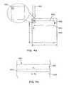
- FIGS. 4 a and 4 bare illustrative diagrams of a crystallized silicon film to be processed by the system of FIG. 3 using a narrow beam;
- FIG. 5is an illustrative diagram of a crystallized silicon film to be processed by the system of FIG. 3 using a wide beam;
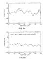
- FIGS. 6-7are charts showing the surface profile of a typical film before and after processing by the system of FIG. 3;
- FIG. 8is an illustrative diagram of a cross section of a crystallized silicon film processed by the system of FIG. 1 in accordance with a second embodiment of the present invention
- FIG. 9is a chart showing the surface profile of a typical film which has been processed in accordance with the second embodiment of the present invention.
- FIG. 10is a flow diagram illustrating the steps implemented in the system of FIG. 3 in accordance with the first embodiment of the present invention.
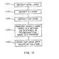
- FIG. 11is a flow diagram illustrating steps implemented in the system of FIG. 1 in accordance with the second embodiment of the present invention.
- the present inventionprovides techniques for planarizing the surfaces of polycrystalline and single crystal thin film semiconductors.
- the surface planarization techniquesare applied as a post processing step to polycrystalline and single crystal thin film semiconductors that are produced during a sequential lateral solidification process, or as a processing step during the production of polycrystalline and single crystal thin film semiconductors in a sequential lateral solidification process. Accordingly, in order to fully understand those techniques, the sequential lateral solidification process must first be appreciated.
- the sequential lateral solidification processis a technique for producing large grained silicon structures through small-scale unidirectional translation of a silicon sample in between sequential pulses emitted by an excimer laser. As each pulse is absorbed by the sample, a small area of the sample is caused to melt completely and resolidify laterally into a crystal region produced by the preceding pulses of a pulse set.
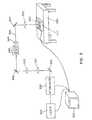
- our co-pending patent applicationdescribes as a preferred embodiment a system including excimer laser 110 , energy density modulator 120 to rapidly change the energy density of laser beam 111 , beam attenuation and shutter 130 , optics 140 , 141 , 142 and 143 , beam homogenizer 144 , lens system 145 , 146 , 148 , masking system 150 , lens system 161 , 162 , 163 , incident laser pulse 164 , thin silicon film sample 170 , sample translation stage 180 , granite block 190 , support system 191 , 192 , 193 , 194 , 195 , 196 , and managing computer 100 X and Y direction translation of the silicon sample 170 may be effected by either movement of a mask 710 within masking system 150 or by movement of the sample translation stage 180 under the direction of computer 100 .
- an amorphous silicon thin film sampleis processed into a single or polycrystalline silicon thin film by generating a plurality of excimer laser pulses of a predetermined fluence, controllably modulating the fluence of the excimer laser pulses, homogenizing the modulated laser pulses in a predetermined plane, masking portions of the homogenized modulated laser pulses into patterned beamlets, irradiating an amorphous silicon thin film sample with the patterned beamlets to effect melting of portions thereof corresponding to the beamlets, and controllably translating the sample with respect to the patterned beamlets and with respect to the controlled modulation to thereby process the amorphous silicon thin film sample into a single or polycrystalline silicon thin film by sequential translation of the sample relative to the patterned beamlets and irradiation of the sample by patterned beamlets of varying fluence at corresponding sequential locations thereon.
- a 200 nm thick crystalwill exhibit variations in height throughout the length of the crystal.
- a height of 0indicates the optimal height in a 200 nm thick crystal, and heights varying from 175 to 225 nm are shown to be common throughout the length of the crystal.
- FIG. 3illustrates a post processing system embodiment for planarizing polycrystalline and single crystal thin film semiconductors produced by the sequential lateral solidification process.
- the systemincludes an excimer laser 310 , beam attenuator and shutter 320 , reflecting plate 330 , telescoping lenses 331 , 332 , reflecting plate 333 , beam homogenizer 340 , condensing lens 345 , reflecting plate 347 , field lense 350 , sample 360 , sample translation stage 370 , optical table 380 , and managing computer 300 .
- a preferred laser 310 , attenuator 320 , telescoping lenses 332 , 332 , homogenizer 340 , and sample translation stage 370 that is movable in two orthogonal directionsare each described in the co-pending patent application Ser. No. 09/390,537.
- the table 380may be as described in that patent document, or may be an ordinary table. It is preferable that the homogenized beam 346 be shaped with a tophat profile in both the x and y directions, and essential that the beam energy density is below that required to completely melt the sample 360 .
- the sample 360is shown in greater detail. Since the sample in this embodiment has already been processed, it already includes a large number of single crystal regions, shown illustratively as chevron shaped crystals 365 .
- the homogenized beam 346is shown incident upon a portion 361 of sample 360 to induce partial melting thereof.
- the full melt thresholdis approximately 600 mJ/cm2.
- a beam 346 having an energy that is approximately 25% to 75% of the full melt thresholdshould be utilized. If the beam is more energetic, energy fluctuations inherent in excimer lasers create the possibility of causing a full melt of the sample region 361 . If the beam is less energetic, the sample portion 361 will not melt sufficiently to satisfactorily planarize.
- the sample 360includes a silicon oxide base layer 400 and a silicon layer 410 .
- the outer surface of silicon layer 410is caused to melt to a depth 420 .
- the rough surface 430is reformed in a more planarized manner.
- a single homogenized beam pulse having an energy that is approximately 25% to 75% of the full melt thresholdis sufficient to induce partial melting of the region 361
- multiple beam pulsesare caused to irradiate every such region.
- Each subsequent beam pulsewill induce partial melting of the region 361 , which upon resolidification will exhibit a more planarized surface.
- the use of ten beam pulses per region 361will produce a far smoother surface 430 than would the use of a single pulse.
- the sample stage 370is translated, under the control of computer 300 , from right to left to cause the homogenized beam 346 to scan the sample 360 from left to right 450 on the top of sample 360 .
- the stage 370is then moved in an orthogonal direction (shown as the Y direction) to realign the sample at a new position 460 , and translation in the opposite direction is began 470 . This processes is repeated until the entire surface of sample 360 has been scanned by the homogenized beam 346 .
- the sample stageWhen the sample stage is translated in the Y direction, it may be advantageous to align the homogenized beam to slightly overlap a previously scanned region of the sample 360 .
- the region 361is 1.2 ⁇ 1.2 cm
- Y direction translation of 1.15 cmmay be utilized to avoid edge effects caused by irregularities in the homogenized beam.
- a wide homogenized beam 500which is sufficiently wide to eliminated the need for X direction translation may be utilized, with the benefit of necessitating less movement by the translation stage 360 , and adoringly, greater throughput.
- a beam that is shaped with a Gaussian profile in the X directioncould be utilized if greater overlaps between X translations are performed.
- FIGS. 6-7the results of the process described with reference to FIGS. 3-4 a are illustrated.
- the profile of a sample 360 fabricated in accordance with the sequential lateral solidification processis shown in FIG. 6 a .
- the sampleexhibits surface irregularities of +/ ⁇ 25 nm from the optimal 200 nm height.
- FIG. 6 bafter post processing with a single laser pulse in accordance with the present invention, those surface irregularities are markedly reduced.
- FIG. 8shows a thin silicon sample formed of an approximately 50-200 nm thick amorphous silicon layer 810 deposited on a silicon oxide base layer 820 .
- the sampleis capped with a thick second silicon oxide layer 820 , approximately 2 microns thick, which is substantially rigid.
- the cap layermust be sufficiently thick to withstand the contractions and expansions during melting and resolidification of the silicon layer during the sequential lateral solidification process.
- the sample with cap layer 830are then used in place of sample 170 in the lateral solidification process, a complete description of which is contained in the above mentioned patent application Ser. No. 09/390,537.
- the cap layer 830is removed from the sample by traditional wet or dry etching techniques. As shown in FIG. 9, the results of the process described with reference to FIG. 8 is illustrated.
- the various electronics of the systemare initialized 1000 by the computer 300 to initiate the process.
- a sampleis then loaded onto the sample translation stage 1005 . It should be noted that such loading may be either manual or robotically implemented under the control of computer 300 .
- the sampleis processed in accordance with the sequential lateral solidification process using the apparatus of FIG. 1 1010 .
- the processed sampleis positioned for planarization 1015 .
- the various optical components of the systemare focused 1020 if necessary.
- the laseris then stabilized 1025 to a desired energy level and reputation rate, as needed to partially melt the sample in accordance with the teachings of the present invention. If necessary, the attenuation of the laser pulses is finely adjusted 1030 .
- translation of the sampleis commenced 1035 at a predetermined speed and in a predetermined direction, in accordance with the previously sequential lateral solidification processed regions of the sample.
- the shutteris opened 1040 to expose the sample to irradiation and accordingly, to commence the planarization process.
- FIG. 10is a flow diagram illustrating the basic steps implemented in the system of FIG. 1 using a capped sample as illustrated in FIG. 8 .
- An oxide layeris deposited on a base 1100 .
- a silicon layeris then deposited on the oxide buffer layer 1110 , and a cap oxide is deposited at the top layer of the sample 1120 .
- the sampleis processed in accordance with the sequential lateral solidification process using the apparatus of FIG. 1 1030 .
- the cap oxideis removed, e.g., by a dilute hydrofluoric acid solution.
Landscapes
- Engineering & Computer Science (AREA)
- Physics & Mathematics (AREA)
- Optics & Photonics (AREA)
- Microelectronics & Electronic Packaging (AREA)
- Manufacturing & Machinery (AREA)
- Computer Hardware Design (AREA)
- General Physics & Mathematics (AREA)
- Power Engineering (AREA)
- Condensed Matter Physics & Semiconductors (AREA)
- Plasma & Fusion (AREA)
- Mechanical Engineering (AREA)
- Chemical & Material Sciences (AREA)
- Crystallography & Structural Chemistry (AREA)
- Recrystallisation Techniques (AREA)
Abstract
Description
The U.S. Government has certain rights in this invention pursuant to the terms of the Defense Advanced Research Project Agency award number N66001-98-1-8913.
I. Field of the Invention
The present invention relates to techniques for semiconductor processing, and more particularly to semiconductor processing which may be performed at low temperatures.
II. Description of the Related Art
In the field of semiconductor processing, there have been several attempts to use lasers to convert thin amorphous silicon films into polycrystalline films. An overview of conventional excimer laser annealing technology is presented by James Im et al. in “Crystalline Si Films for Integrated Active-Matrix Liquid-Crystal Displays,” 11 MRS Bulletin 39 (19%). In systems used for carrying out excimer laser annealing, an excimer laser beam is shaped into a long beam which is typically up to 30 cm long and 500 micrometers or greater in width. The shaped beam is scanned over a sample of amorphous silicon to facilitate melting thereof and the formation of polycrystalline silicon upon resolidification of the sample.
The use of conventional excimer laser annealing technology to generate polycrystalline or single crystal silicon is problematic for several reasons. First, the silicon generated in the process is typically small grained, of a random microstructure, and/or has non-uniform grain sizes, which result in poor and non-uniform devices that lead to low manufacturing yield. Second, the processing techniques needed to obtain acceptable performance levels require that the manufacturing throughput for producing polycrystalline silicon be kept low. Also, these processes generally require a controlled atmosphere and preheating of the amorphous silicon sample, which lead to a further reduction in throughput rates. Finally, the fabricated films generally exhibit an unacceptable degree of surface roughness that can be problematic for performance of microelectronic devices.
There exists a need in the field to generate higher quality polycrystalline silicon and single crystal silicon at greater throughput rates. As well, there exists a need for manufacturing techniques that reduce the surface roughness of such polycrystalline and single crystal silicon thin films to be used in the fabrication of higher quality devices, such as flat panel displays.
An object of the present invention is to provide techniques for planarizing the surfaces of polycrystalline and single crystal thin film semiconductors.
A further object of the present invention is to provide surface planarization techniques that may be applied as a post processing step to polycrystalline and single crystal thin film semiconductors that are produced during a sequential lateral solidification process.
Yet a further object of the present invention is to provide surface planarization techniques that may be applied as a processing step during the production of polycrystalline and single crystal thin film semiconductors in a sequential lateral solidification process.
Yet another object of the present invention is to provide techniques for the fabrication of high quality semiconductors devices useful for fabricating displays and other products.
In order to achieve these objectives as well as others that will become apparent with reference to the following specification, the present invention provides systems and methods for reducing surface roughness of a polycrystalline or single crystal thin film that had previously been produced by the sequential lateral solidification process. In one arrangement, the system includes an excimer laser for generating a plurality of excimer laser pulses of a predetermined fluence, an energy density modulator for controllably modulating the fluence of the excimer laser pulses such that the fluence is below that which is required to completely melt the thin film, a beam homogenizer for homogenizing modulated laser pulses in a predetermined plane, a sample stage for receiving homogenized laser pulses to effect partial melting of portions of the polycrystalline or single crystal thin film corresponding to the laser pulses, translating means for controllably translating a relative position of the sample stage with respect to the laser pulses, and a computer for coordinating the excimer pulse generation and fluence modulation with the relative positions of the sample stage to thereby process the polycrystalline or single crystal thin film by sequential translation of the sample stage relative to the laser pulses. The excimer laser is preferably an ultraviolet excimer laser for generating ultraviolet excimer laser pulses.
In one arrangement, the beam homogenizer is operable to shape laser pulses with a tophat profile in both the x and y directions. The energy density modulator is operable to attenuate fluence of the excimer laser pulses to approximately 25% to 75% of the full melt threshold of the polycrystalline or single crystal thin film.
The translating stage advantageously includes an X direction translation portion and a Y direction translation portion, each being coupled to the computer and to each other and permitting movement in two orthogonal directions that are perpendicular to a path formed by the laser pulses, and being controllable by the computer for controllably translating the sample in both of said translatable directions under control of said computer. Also, the beam homogenizer is operable to shape said laser pulses with a tophat profile in both the x and y directions, and the translating means is operable to translate the polycrystalline or single crystal thin film in two directions orthogonal to a direction of said laser pulses such that sequential homogenized laser pulses are incident on slightly overlapping regions of the polycrystalline or single crystal thin film in the two directions.
In an alternative arrangement, the present invention provides for systems and methods for processing an amorphous silicon thin film sample into a single or polycrystalline silicon thin film having a reduced surface roughness. In one arrangement, the method includes forming a rigid cap layer on an amorphous silicon thin film sample having sufficient thickness to withstand contractions and expansions during melting and resolidification of the silicon thin film during the sequential lateral solidification process. The method also includes generating a sequence of excimer laser pulses; controllably modulating each excimer laser pulse in the sequence to a predetermined fluence; homogenizing each modulated laser pulse in the sequence in a predetermined plane; masking portions of each homogenized fluence controlled laser pulse in the sequence to generate a sequence of fluence controlled pulses of patterned beamlets, irradiating the amorphous silicon thin film sample with the sequence of fluence controlled patterned beamlets to effect melting of portions thereof; controllably sequentially translating the sample relative to each of said fluence controlled pulse of patterned beamlets to thereby process the amorphous silicon thin film sample into a single or polycrystalline silicon thin film having a reduced surface roughness; and removing said cap layer from the processed single or polycrystalline silicon thin film.
The accompanying drawings, which are incorporated and constitute part of this disclosure, illustrate a preferred embodiment of the invention and serve to explain the principles of the invention.
FIG. 1 is a functional diagram of a system for performing the sequential lateral solidification process preferred to implement a preferred process of the present invention;
FIG. 2 is a chart showing the surface profile of a typical film which has been processed by the sequential lateral solidification system of FIG. 1;
FIG. 3 is a functional diagram of a preferred system for planarizing the surface of a polycrystalline or single crystal thin film semiconductor produced during a sequential lateral solidification process in accordance with the present invention,
FIGS. 4aand4bare illustrative diagrams of a crystallized silicon film to be processed by the system of FIG. 3 using a narrow beam;
FIG. 5 is an illustrative diagram of a crystallized silicon film to be processed by the system of FIG. 3 using a wide beam;
FIGS. 6-7 are charts showing the surface profile of a typical film before and after processing by the system of FIG. 3;
FIG. 8 is an illustrative diagram of a cross section of a crystallized silicon film processed by the system of FIG. 1 in accordance with a second embodiment of the present invention;
FIG. 9 is a chart showing the surface profile of a typical film which has been processed in accordance with the second embodiment of the present invention.
FIG. 10 is a flow diagram illustrating the steps implemented in the system of FIG. 3 in accordance with the first embodiment of the present invention; and
FIG. 11 is a flow diagram illustrating steps implemented in the system of FIG. 1 in accordance with the second embodiment of the present invention.
The present invention provides techniques for planarizing the surfaces of polycrystalline and single crystal thin film semiconductors. In the preferred embodiments, the surface planarization techniques are applied as a post processing step to polycrystalline and single crystal thin film semiconductors that are produced during a sequential lateral solidification process, or as a processing step during the production of polycrystalline and single crystal thin film semiconductors in a sequential lateral solidification process. Accordingly, in order to fully understand those techniques, the sequential lateral solidification process must first be appreciated.
The sequential lateral solidification process is a technique for producing large grained silicon structures through small-scale unidirectional translation of a silicon sample in between sequential pulses emitted by an excimer laser. As each pulse is absorbed by the sample, a small area of the sample is caused to melt completely and resolidify laterally into a crystal region produced by the preceding pulses of a pulse set.
A particularly advantageous sequential lateral solidification process and an apparatus to carry out that process are disclosed in our co-pending patent application Ser. No. 09/390,537, filed Sep. 3, 1999, entitled “Systems and Methods using Sequential Lateral Solidification for Producing Single or Polycrystalline Silicon Thin Films at Low Temperatures,” the disclosure of which is incorporated by reference herein. While the foregoing disclosure is made with reference to the particular techniques described in our co-pending patent application, it should be understood that other sequential lateral solidification techniques could readily be adapted for use in the present invention.
With reference to FIG. 1, our co-pending patent application describes as a preferred embodiment a system includingexcimer laser 110,energy density modulator 120 to rapidly change the energy density oflaser beam 111, beam attenuation andshutter 130,optics beam homogenizer 144,lens system masking system 150,lens system incident laser pulse 164, thinsilicon film sample 170,sample translation stage 180,granite block 190,support system silicon sample 170 may be effected by either movement of a mask710 withinmasking system 150 or by movement of thesample translation stage 180 under the direction ofcomputer 100.
As described in further detail in our co-pending application, an amorphous silicon thin film sample is processed into a single or polycrystalline silicon thin film by generating a plurality of excimer laser pulses of a predetermined fluence, controllably modulating the fluence of the excimer laser pulses, homogenizing the modulated laser pulses in a predetermined plane, masking portions of the homogenized modulated laser pulses into patterned beamlets, irradiating an amorphous silicon thin film sample with the patterned beamlets to effect melting of portions thereof corresponding to the beamlets, and controllably translating the sample with respect to the patterned beamlets and with respect to the controlled modulation to thereby process the amorphous silicon thin film sample into a single or polycrystalline silicon thin film by sequential translation of the sample relative to the patterned beamlets and irradiation of the sample by patterned beamlets of varying fluence at corresponding sequential locations thereon.
While the sequential lateral solidification process is highly advantageous to produce single crystal or large grained polycrystalline silicon thin films, the produced crystals often exhibit a surface roughness due to the irrative nature of the melting and resolidification inherent in the crystal growth process. Thus, as shown in FIG. 2, a 200 nm thick crystal will exhibit variations in height throughout the length of the crystal. In FIG. 2, a height of 0 indicates the optimal height in a 200 nm thick crystal, and heights varying from 175 to 225 nm are shown to be common throughout the length of the crystal. Note the large bump210 near the crystal boundary, where crystal thickness exceeds the optimal 200 nm thickness by 350 nm.
Referring to FIGS. 3 and 4, a first embodiment of the present invention will now be described. FIG. 3 illustrates a post processing system embodiment for planarizing polycrystalline and single crystal thin film semiconductors produced by the sequential lateral solidification process. The system includes anexcimer laser 310, beam attenuator andshutter 320, reflectingplate 330,telescoping lenses plate 333,beam homogenizer 340,condensing lens 345, reflectingplate 347,field lense 350,sample 360,sample translation stage 370, optical table380, and managingcomputer 300. Apreferred laser 310,attenuator 320,telescoping lenses homogenizer 340, andsample translation stage 370 that is movable in two orthogonal directions are each described in the co-pending patent application Ser. No. 09/390,537. The table380 may be as described in that patent document, or may be an ordinary table. It is preferable that thehomogenized beam 346 be shaped with a tophat profile in both the x and y directions, and essential that the beam energy density is below that required to completely melt thesample 360.
With reference to FIGS. 4aand4b, thesample 360 is shown in greater detail. Since the sample in this embodiment has already been processed, it already includes a large number of single crystal regions, shown illustratively as chevron shapedcrystals 365. Thehomogenized beam 346 is shown incident upon aportion 361 ofsample 360 to induce partial melting thereof.
For a 200 nm thick silicon thin film, the full melt threshold is approximately 600 mJ/cm2. Thus, to induce sufficient partial melting of theportion 361, abeam 346 having an energy that is approximately 25% to 75% of the full melt threshold should be utilized. If the beam is more energetic, energy fluctuations inherent in excimer lasers create the possibility of causing a full melt of thesample region 361. If the beam is less energetic, thesample portion 361 will not melt sufficiently to satisfactorily planarize.
As shown in FIG. 4b, thesample 360 includes a siliconoxide base layer 400 and asilicon layer 410. In accordance with the present invention, the outer surface ofsilicon layer 410 is caused to melt to adepth 420. Upon resolidification, therough surface 430 is reformed in a more planarized manner.
While a single homogenized beam pulse having an energy that is approximately 25% to 75% of the full melt threshold is sufficient to induce partial melting of theregion 361, it is preferred that multiple beam pulses are caused to irradiate every such region. Each subsequent beam pulse will induce partial melting of theregion 361, which upon resolidification will exhibit a more planarized surface. Thus, the use of ten beam pulses perregion 361 will produce a farsmoother surface 430 than would the use of a single pulse.
Returning to FIG. 4a, thesample stage 370 is translated, under the control ofcomputer 300, from right to left to cause thehomogenized beam 346 to scan thesample 360 from left to right450 on the top ofsample 360. Thestage 370 is then moved in an orthogonal direction (shown as the Y direction) to realign the sample at anew position 460, and translation in the opposite direction is began470. This processes is repeated until the entire surface ofsample 360 has been scanned by thehomogenized beam 346.
When the sample stage is translated in the Y direction, it may be advantageous to align the homogenized beam to slightly overlap a previously scanned region of thesample 360. Thus, if theregion 361 is 1.2×1.2 cm, Y direction translation of 1.15 cm may be utilized to avoid edge effects caused by irregularities in the homogenized beam. Likewise, it is advantageous to cause a slight overlap with X-direction translation is being effected.
While the foregoing has been described with respect to a tophat profile square homogenized beam, beams of other shapes may be utilized. Thus, as shown in FIG. 5, a widehomogenized beam 500 which is sufficiently wide to eliminated the need for X direction translation may be utilized, with the benefit of necessitating less movement by thetranslation stage 360, and adoringly, greater throughput. Likewise, a beam that is shaped with a Gaussian profile in the X direction could be utilized if greater overlaps between X translations are performed.
As shown in FIGS. 6-7, the results of the process described with reference to FIGS. 3-4aare illustrated. The profile of asample 360 fabricated in accordance with the sequential lateral solidification process is shown in FIG. 6a. The sample exhibits surface irregularities of +/−25 nm from the optimal 200 nm height. As shown in FIG. 6b, after post processing with a single laser pulse in accordance with the present invention, those surface irregularities are markedly reduced. These results are alternatively illustrated in FIG. 7, where it is shown >100% decrease in surface roughness caused by post processing in accordance with the invention herein.
Referring next to FIG. 8, a second embodiment of the present invention will now be described. In this embodiment, the surface of silicon thin film is kept planarized through the employment of a rigid cap layer during the sequential lateral solidification process. Thus, FIG. 8 shows a thin silicon sample formed of an approximately 50-200 nm thickamorphous silicon layer 810 deposited on a siliconoxide base layer 820. The sample is capped with a thick secondsilicon oxide layer 820, approximately 2 microns thick, which is substantially rigid. The cap layer must be sufficiently thick to withstand the contractions and expansions during melting and resolidification of the silicon layer during the sequential lateral solidification process.
The sample with cap layer830 are then used in place ofsample 170 in the lateral solidification process, a complete description of which is contained in the above mentioned patent application Ser. No. 09/390,537. After such processing, the cap layer830 is removed from the sample by traditional wet or dry etching techniques. As shown in FIG. 9, the results of the process described with reference to FIG. 8 is illustrated.
Referring to FIG. 10, the steps executed bycomputer 300 to control both the sequential lateral solidification process of FIG.1 and the surface planarization process implemented with respect to FIG. 3 will be described. The various electronics of the system are initialized1000 by thecomputer 300 to initiate the process. A sample is then loaded onto thesample translation stage 1005. It should be noted that such loading may be either manual or robotically implemented under the control ofcomputer 300. Next, the sample is processed in accordance with the sequential lateral solidification process using the apparatus of FIG. 11010. The processed sample is positioned forplanarization 1015. The various optical components of the system are focused1020 if necessary. The laser is then stabilized1025 to a desired energy level and reputation rate, as needed to partially melt the sample in accordance with the teachings of the present invention. If necessary, the attenuation of the laser pulses is finely adjusted1030.
Next, translation of the sample is commenced1035 at a predetermined speed and in a predetermined direction, in accordance with the previously sequential lateral solidification processed regions of the sample. The shutter is opened1040 to expose the sample to irradiation and accordingly, to commence the planarization process.
Sample translation and irradiation continues until planarization has been competed1045,105, at which time the computer closes the shutter and stopstranslation
Referring next to FIG. 11, the steps executed bycomputer 100 to control the crystal growth process with the surface planarization steps implemented with respect to FIG. 1 will be described. FIG. 10 is a flow diagram illustrating the basic steps implemented in the system of FIG. 1 using a capped sample as illustrated in FIG.8. An oxide layer is deposited on abase 1100. A silicon layer is then deposited on theoxide buffer layer 1110, and a cap oxide is deposited at the top layer of thesample 1120.
Next, the sample is processed in accordance with the sequential lateral solidification process using the apparatus of FIG. 11030. After processing, the cap oxide is removed, e.g., by a dilute hydrofluoric acid solution.
The foregoing merely illustrates the principles of the invention. Various modifications and alterations to the described embodiments will be apparent to those skilled in the art in view of the teachings herein. For example, while removal of the cap layer had been disclosed with respect to use of a dilute hydrofluoric acid solution, the cap layer may be removed by any conventional technique such as dry etching. It will thus be appreciated that those skilled in the art will be able to devise numerous systems and methods which, although not explicitly shown or described herein, embody the principles of the invention and are thus within the spirit and scope of the invention.
Claims (9)
1. A method for reducing a surface roughness of a polycrystalline or single crystal thin film produced by the sequential lateral solidification process, comprising the steps of:
(a) generating a plurality of excimer laser pulses of a predetermined fluence;
(b) controllably modulating said fluence of said excimer laser pulses emitted by said excimer laser such that said fluence is below that which is required to completely melt said polycrystalline or single crystal thin film;
(c) homogenizing said modulated laser pulses in a predetermined plane;
(d) effecting partial melting of portions of said polycrystalline or single crystal thin film corresponding to said homogenized laser pulses; and
(e) controllably translating a relative position of said polycrystalline or single crystal thin film with respect to said homogenized laser pulses to process said polycrystalline or single crystal thin film by sequential translation of said sample stage relative to said homogenized laser pulses at corresponding sequential locations thereon.
2. The method ofclaim 1 , wherein said excimer laser pulses comprise ultraviolet excimer laser pulses.
3. The method ofclaim 1 , wherein said homogenizing step comprises homogenizing said modulated laser pulses with a tophat profile in both the x and y directions.
4. The method ofclaim 1 , wherein said modulating step comprises attenuating said fluence of said excimer laser pulses to approximately 25% to 75% of the full melt threshold of said polycrystalline or single crystal thin film.
5. The method ofclaim 1 , wherein said translating step comprises controllably translating said polycrystalline or single crystal thin film in one direction orthogonal to a direction of said homogenized laser pulses.
6. The method ofclaim 5 , wherein said homogenizing step comprises homogenizing said modulated laser pulses with a tophat profile in at least said direction orthogonal to a direction of said modulated laser pulses, and wherein said translating step comprises translating said polycrystalline or single crystal thin film in said direction orthogonal to a direction of said homogenized laser pulses, such that sequential homogenized laser pulses are incident on slightly overlapping regions of said polycrystalline or single crystal thin film.
7. The method ofclaim 1 , wherein said translating step comprises controllably translating said polycrystalline or single crystal thin film in two orthogonal directions that are perpendicular to a path formed by said homogenized laser pulses.
8. The method ofclaim 7 , wherein said homogenizing step comprises homogenizing said modulated laser pulses with a tophat profile in said two directions orthogonal to a direction of said modulated laser pulses, and wherein said translating step comprises translating said polycrystalline or single crystal thin film in said two directions such that sequential homogenized laser pulses are incident on slightly overlapping regions of said polycrystalline or single crystal thin film in said two directions.
9. The method ofclaim 1 , wherein said translating step comprises translating said polycrystalline or single crystal thin film after at least two homogenized beam pulses irradiate said portion of said polycrystalline or single crystal thin film.
Priority Applications (3)
| Application Number | Priority Date | Filing Date | Title |
|---|---|---|---|
| US09/979,201US6830993B1 (en) | 2000-03-21 | 2000-03-21 | Surface planarization of thin silicon films during and after processing by the sequential lateral solidification method |
| US10/939,271US7220660B2 (en) | 2000-03-21 | 2004-09-13 | Surface planarization of thin silicon films during and after processing by the sequential lateral solidification method |
| US11/671,917US7704862B2 (en) | 2000-03-21 | 2007-02-06 | Surface planarization of thin silicon films during and after processing by the sequential lateral solidification method |
Applications Claiming Priority (2)
| Application Number | Priority Date | Filing Date | Title |
|---|---|---|---|
| PCT/US2000/007479WO2001071791A1 (en) | 2000-03-21 | 2000-03-21 | Surface planarization of thin silicon films during and after processing by the sequential lateral solidification method |
| US09/979,201US6830993B1 (en) | 2000-03-21 | 2000-03-21 | Surface planarization of thin silicon films during and after processing by the sequential lateral solidification method |
Related Child Applications (1)
| Application Number | Title | Priority Date | Filing Date |
|---|---|---|---|
| US10/939,271DivisionUS7220660B2 (en) | 2000-03-21 | 2004-09-13 | Surface planarization of thin silicon films during and after processing by the sequential lateral solidification method |
Publications (1)
| Publication Number | Publication Date |
|---|---|
| US6830993B1true US6830993B1 (en) | 2004-12-14 |
Family
ID=33491132
Family Applications (3)
| Application Number | Title | Priority Date | Filing Date |
|---|---|---|---|
| US09/979,201Expired - LifetimeUS6830993B1 (en) | 2000-03-21 | 2000-03-21 | Surface planarization of thin silicon films during and after processing by the sequential lateral solidification method |
| US10/939,271Expired - Fee RelatedUS7220660B2 (en) | 2000-03-21 | 2004-09-13 | Surface planarization of thin silicon films during and after processing by the sequential lateral solidification method |
| US11/671,917Expired - Fee RelatedUS7704862B2 (en) | 2000-03-21 | 2007-02-06 | Surface planarization of thin silicon films during and after processing by the sequential lateral solidification method |
Family Applications After (2)
| Application Number | Title | Priority Date | Filing Date |
|---|---|---|---|
| US10/939,271Expired - Fee RelatedUS7220660B2 (en) | 2000-03-21 | 2004-09-13 | Surface planarization of thin silicon films during and after processing by the sequential lateral solidification method |
| US11/671,917Expired - Fee RelatedUS7704862B2 (en) | 2000-03-21 | 2007-02-06 | Surface planarization of thin silicon films during and after processing by the sequential lateral solidification method |
Country Status (1)
| Country | Link |
|---|---|
| US (3) | US6830993B1 (en) |
Cited By (37)
| Publication number | Priority date | Publication date | Assignee | Title |
|---|---|---|---|---|
| US20030096489A1 (en)* | 1999-09-03 | 2003-05-22 | Im James S. | Methods for producing uniform large-grained and grain boundary location manipulated polycrystalline thin film semiconductors using sequential lateral solidification |
| US20040061843A1 (en)* | 2000-11-27 | 2004-04-01 | Im James S. | Process and mask projection system for laser crystallization processing of semiconductor film regions on a substrate |
| US20050032249A1 (en)* | 2000-03-21 | 2005-02-10 | Im James S. | Surface planarization of thin silicon films during and after processing by the sequential lateral solidification method |
| US20050034653A1 (en)* | 2001-08-27 | 2005-02-17 | James Im | Polycrystalline tft uniformity through microstructure mis-alignment |
| US20050202654A1 (en)* | 2002-08-19 | 2005-09-15 | Im James S. | Process and system for laser crystallization processing of film regions on a substrate to provide substantial uniformity, and a structure of such film regions |
| US20060006464A1 (en)* | 2002-04-01 | 2006-01-12 | Im James S | Method and system for providing a thin film with a controlled crystal orientation using pulsed laser induced melting and nucleation-initiated crystallization |
| US20060030164A1 (en)* | 2002-08-19 | 2006-02-09 | Im James S | Process and system for laser crystallization processing of film regions on a substrate to minimize edge areas, and a structure of such film regions |
| US20060060130A1 (en)* | 2002-08-19 | 2006-03-23 | Im James S | Process and system for laser crystallization processing of film regions on a substrate to provide substantial uniformity within arears in such regions and edge areas thereof, and a structure of film regions |
| US20060134890A1 (en)* | 2003-02-19 | 2006-06-22 | Im James S | System and process for processing a plurality of semiconductor thin films which are crystallized using sequential lateral solidification techniques |
| US7115503B2 (en) | 2000-10-10 | 2006-10-03 | The Trustees Of Columbia University In The City Of New York | Method and apparatus for processing thin metal layers |
| US7164152B2 (en) | 2003-09-16 | 2007-01-16 | The Trustees Of Columbia University In The City Of New York | Laser-irradiated thin films having variable thickness |
| US20070032096A1 (en)* | 2003-09-16 | 2007-02-08 | Im James S | System and process for providing multiple beam sequential lateral solidification |
| US20070281172A1 (en)* | 2006-05-31 | 2007-12-06 | James Gregory Couillard | Semiconductor on insulator structure made using radiation annealing |
| US7311778B2 (en) | 2003-09-19 | 2007-12-25 | The Trustees Of Columbia University In The City Of New York | Single scan irradiation for crystallization of thin films |
| US7318866B2 (en) | 2003-09-16 | 2008-01-15 | The Trustees Of Columbia University In The City Of New York | Systems and methods for inducing crystallization of thin films using multiple optical paths |
| US7364952B2 (en) | 2003-09-16 | 2008-04-29 | The Trustees Of Columbia University In The City Of New York | Systems and methods for processing thin films |
| WO2007067541A3 (en)* | 2005-12-05 | 2009-04-30 | Univ Columbia | Systems and methods for processing a film, and thin films |
| US7638728B2 (en) | 2003-09-16 | 2009-12-29 | The Trustees Of Columbia University In The City Of New York | Enhancing the width of polycrystalline grains with mask |
| US7645337B2 (en)* | 2004-11-18 | 2010-01-12 | The Trustees Of Columbia University In The City Of New York | Systems and methods for creating crystallographic-orientation controlled poly-silicon films |
| US7718517B2 (en) | 2002-08-19 | 2010-05-18 | Im James S | Single-shot semiconductor processing system and method having various irradiation patterns |
| US7759230B2 (en) | 2003-09-16 | 2010-07-20 | The Trustees Of Columbia University In The City Of New York | System for providing a continuous motion sequential lateral solidification for reducing or eliminating artifacts in overlap regions, and a mask for facilitating such artifact reduction/elimination |
| US8012861B2 (en) | 2007-11-21 | 2011-09-06 | The Trustees Of Columbia University In The City Of New York | Systems and methods for preparing epitaxially textured polycrystalline films |
| US8221544B2 (en) | 2005-04-06 | 2012-07-17 | The Trustees Of Columbia University In The City Of New York | Line scan sequential lateral solidification of thin films |
| US8415670B2 (en) | 2007-09-25 | 2013-04-09 | The Trustees Of Columbia University In The City Of New York | Methods of producing high uniformity in thin film transistor devices fabricated on laterally crystallized thin films |
| US8426296B2 (en) | 2007-11-21 | 2013-04-23 | The Trustees Of Columbia University In The City Of New York | Systems and methods for preparing epitaxially textured polycrystalline films |
| US8440581B2 (en) | 2009-11-24 | 2013-05-14 | The Trustees Of Columbia University In The City Of New York | Systems and methods for non-periodic pulse sequential lateral solidification |
| US8557040B2 (en) | 2007-11-21 | 2013-10-15 | The Trustees Of Columbia University In The City Of New York | Systems and methods for preparation of epitaxially textured thick films |
| US8569155B2 (en) | 2008-02-29 | 2013-10-29 | The Trustees Of Columbia University In The City Of New York | Flash lamp annealing crystallization for large area thin films |
| US8614471B2 (en) | 2007-09-21 | 2013-12-24 | The Trustees Of Columbia University In The City Of New York | Collections of laterally crystallized semiconductor islands for use in thin film transistors |
| US8663387B2 (en) | 2003-09-16 | 2014-03-04 | The Trustees Of Columbia University In The City Of New York | Method and system for facilitating bi-directional growth |
| US8796159B2 (en) | 2003-09-16 | 2014-08-05 | The Trustees Of Columbia University In The City Of New York | Processes and systems for laser crystallization processing of film regions on a substrate utilizing a line-type beam, and structures of such film regions |
| US8802580B2 (en) | 2008-11-14 | 2014-08-12 | The Trustees Of Columbia University In The City Of New York | Systems and methods for the crystallization of thin films |
| FR3002687A1 (en)* | 2013-02-26 | 2014-08-29 | Soitec Silicon On Insulator | PROCESS FOR TREATING A STRUCTURE |
| EP2881213A1 (en)* | 2013-12-05 | 2015-06-10 | Samsung Display Co., Ltd. | Laser crystallization apparatus and organic light-emitting diode (oled) display manufactured using the same |
| US9087696B2 (en) | 2009-11-03 | 2015-07-21 | The Trustees Of Columbia University In The City Of New York | Systems and methods for non-periodic pulse partial melt film processing |
| US9646831B2 (en) | 2009-11-03 | 2017-05-09 | The Trustees Of Columbia University In The City Of New York | Advanced excimer laser annealing for thin films |
| CN113557469A (en)* | 2019-03-12 | 2021-10-26 | 思科技术公司 | Optical modulator with epitaxially regrown regions over polysilicon |
Families Citing this family (25)
| Publication number | Priority date | Publication date | Assignee | Title |
|---|---|---|---|---|
| US7057256B2 (en)* | 2001-05-25 | 2006-06-06 | President & Fellows Of Harvard College | Silicon-based visible and near-infrared optoelectric devices |
| US7390689B2 (en)* | 2001-05-25 | 2008-06-24 | President And Fellows Of Harvard College | Systems and methods for light absorption and field emission using microstructured silicon |
| US7442629B2 (en) | 2004-09-24 | 2008-10-28 | President & Fellows Of Harvard College | Femtosecond laser-induced formation of submicrometer spikes on a semiconductor substrate |
| WO2005029550A2 (en)* | 2003-09-16 | 2005-03-31 | The Trustees Of Columbia University In The City Of New York | Method and system for producing crystalline thin films with a uniform crystalline orientation |
| DE102005020072B4 (en)* | 2005-04-22 | 2007-12-06 | Forschungsverbund Berlin E.V. | Process for fine polishing / structuring heat-sensitive dielectric materials by means of laser radiation |
| TWI524384B (en)* | 2005-08-16 | 2016-03-01 | 紐約市哥倫比亞大學理事會 | High-capacity crystallization of the film layer |
| EP1922745A1 (en)* | 2005-08-16 | 2008-05-21 | The Trustees of Columbia University in the City of New York | Systems and methods for uniform sequential lateral solidification of thin films using high frequency lasers |
| JP2009135453A (en)* | 2007-10-30 | 2009-06-18 | Semiconductor Energy Lab Co Ltd | Method for manufacturing semiconductor device, semiconductor device, and electronic device |
| CN102017088B (en)* | 2008-01-31 | 2013-08-07 | 哈佛大学校长及研究员协会 | Structure flat surfaces on materials doped by pulsed laser irradiation |
| WO2009111326A2 (en)* | 2008-02-29 | 2009-09-11 | The Trustees Of Columbia University In The City Of New York | Flash light annealing for thin films |
| US20110175099A1 (en)* | 2008-02-29 | 2011-07-21 | The Trustees Of Columbia University In The City Of New York | Lithographic method of making uniform crystalline si films |
| SG160310A1 (en)* | 2008-10-02 | 2010-04-29 | Semiconductor Energy Lab | Manufacturing method of semiconductor substrate and semiconductor device |
| US8999823B2 (en) | 2008-10-23 | 2015-04-07 | Sharp Kabushiki Kaisha | Semiconductor device, method for manufacturing same, and display device |
| US20110068342A1 (en)* | 2009-09-18 | 2011-03-24 | Themistokles Afentakis | Laser Process for Minimizing Variations in Transistor Threshold Voltages |
| WO2011056787A1 (en)* | 2009-11-03 | 2011-05-12 | The Trustees Of Columbia University In The City Of New York | Systems and methods for non-periodic pulse partial melt film processing |
| US8692198B2 (en) | 2010-04-21 | 2014-04-08 | Sionyx, Inc. | Photosensitive imaging devices and associated methods |
| WO2011160130A2 (en) | 2010-06-18 | 2011-12-22 | Sionyx, Inc | High speed photosensitive devices and associated methods |
| US9496308B2 (en) | 2011-06-09 | 2016-11-15 | Sionyx, Llc | Process module for increasing the response of backside illuminated photosensitive imagers and associated methods |
| WO2013010127A2 (en) | 2011-07-13 | 2013-01-17 | Sionyx, Inc. | Biometric imaging devices and associated methods |
| KR20140142856A (en)* | 2013-06-05 | 2014-12-15 | 삼성디스플레이 주식회사 | Laser apparatus and method of crystallizing |
| US9209345B2 (en) | 2013-06-29 | 2015-12-08 | Sionyx, Inc. | Shallow trench textured regions and associated methods |
| US9455350B2 (en) | 2014-03-25 | 2016-09-27 | National Applied Research Laboratories | Transistor device structure that includes polycrystalline semiconductor thin film that has large grain size |
| KR102293732B1 (en) | 2014-10-08 | 2021-08-27 | 삼성디스플레이 주식회사 | Thin film transistor substrate, display apparatus comprising the same, method for manufacturing thin film transistor substrate, and method for manufacturing display apparatus |
| US10629434B2 (en) | 2015-04-08 | 2020-04-21 | The Trustees Of Columbia University In The City Of New York | Laser irradiation induced surface planarization of polycrystalline silicon films |
| JP2017037178A (en) | 2015-08-10 | 2017-02-16 | ルネサスエレクトロニクス株式会社 | Semiconductor device and method for manufacturing the same |
Citations (7)
| Publication number | Priority date | Publication date | Assignee | Title |
|---|---|---|---|---|
| US5523193A (en) | 1988-05-31 | 1996-06-04 | Texas Instruments Incorporated | Method and apparatus for patterning and imaging member |
| US5591668A (en) | 1994-03-14 | 1997-01-07 | Matsushita Electric Industrial Co., Ltd. | Laser annealing method for a semiconductor thin film |
| US6242291B1 (en)* | 1996-12-12 | 2001-06-05 | Semiconductor Energy Laboratory Co., Ltd. | Laser annealing method and laser annealing device |
| US6322625B2 (en)* | 1996-05-28 | 2001-11-27 | The Trustees Of Columbia University In The City Of New York | Crystallization processing of semiconductor film regions on a substrate, and devices made therewith |
| US6444506B1 (en)* | 1995-10-25 | 2002-09-03 | Semiconductor Energy Laboratory Co., Ltd. | Method of manufacturing silicon thin film devices using laser annealing in a hydrogen mixture gas followed by nitride formation |
| US6555449B1 (en)* | 1996-05-28 | 2003-04-29 | Trustees Of Columbia University In The City Of New York | Methods for producing uniform large-grained and grain boundary location manipulated polycrystalline thin film semiconductors using sequential lateral solidfication |
| US6573531B1 (en)* | 1999-09-03 | 2003-06-03 | The Trustees Of Columbia University In The City Of New York | Systems and methods using sequential lateral solidification for producing single or polycrystalline silicon thin films at low temperatures |
Family Cites Families (193)
| Publication number | Priority date | Publication date | Assignee | Title |
|---|---|---|---|---|
| US469183A (en)* | 1892-02-16 | Edwin c | ||
| FR2030468A5 (en) | 1969-01-29 | 1970-11-13 | Thomson Brandt Csf | |
| US4234358A (en) | 1979-04-05 | 1980-11-18 | Western Electric Company, Inc. | Patterned epitaxial regrowth using overlapping pulsed irradiation |
| US4309225A (en) | 1979-09-13 | 1982-01-05 | Massachusetts Institute Of Technology | Method of crystallizing amorphous material with a moving energy beam |
| EP0191503A3 (en) | 1980-04-10 | 1986-09-10 | Massachusetts Institute Of Technology | Method of producing sheets of crystalline material |
| US4382658A (en) | 1980-11-24 | 1983-05-10 | Hughes Aircraft Company | Use of polysilicon for smoothing of liquid crystal MOS displays |
| US4456371A (en) | 1982-06-30 | 1984-06-26 | International Business Machines Corporation | Optical projection printing threshold leveling arrangement |
| JPS59195871A (en) | 1983-04-20 | 1984-11-07 | Mitsubishi Electric Corp | Manufacture of metal oxide semiconductor field-effect transistor |
| US4691983A (en) | 1983-10-14 | 1987-09-08 | Hitachi, Ltd. | Optical waveguide and method for making the same |
| US4639277A (en) | 1984-07-02 | 1987-01-27 | Eastman Kodak Company | Semiconductor material on a substrate, said substrate comprising, in order, a layer of organic polymer, a layer of metal or metal alloy and a layer of dielectric material |
| JPH0433327Y2 (en) | 1985-04-19 | 1992-08-10 | ||
| JPH084067B2 (en) | 1985-10-07 | 1996-01-17 | 工業技術院長 | Method for manufacturing semiconductor device |
| JPH0732124B2 (en) | 1986-01-24 | 1995-04-10 | シャープ株式会社 | Method for manufacturing semiconductor device |
| US4793694A (en) | 1986-04-23 | 1988-12-27 | Quantronix Corporation | Method and apparatus for laser beam homogenization |
| JPS62181419U (en) | 1986-05-12 | 1987-11-18 | ||
| JPS62293740A (en) | 1986-06-13 | 1987-12-21 | Fujitsu Ltd | Manufacture of semiconductor device |
| US4758533A (en) | 1987-09-22 | 1988-07-19 | Xmr Inc. | Laser planarization of nonrefractory metal during integrated circuit fabrication |
| USRE33836E (en) | 1987-10-22 | 1992-03-03 | Mrs Technology, Inc. | Apparatus and method for making large area electronic devices, such as flat panel displays and the like, using correlated, aligned dual optical systems |
| US5204659A (en) | 1987-11-13 | 1993-04-20 | Honeywell Inc. | Apparatus and method for providing a gray scale in liquid crystal flat panel displays |
| JP2569711B2 (en) | 1988-04-07 | 1997-01-08 | 株式会社ニコン | Exposure control device and exposure method using the same |
| JP2706469B2 (en) | 1988-06-01 | 1998-01-28 | 松下電器産業株式会社 | Method for manufacturing semiconductor device |
| US4940505A (en) | 1988-12-02 | 1990-07-10 | Eaton Corporation | Method for growing single crystalline silicon with intermediate bonding agent and combined thermal and photolytic activation |
| US4976809A (en) | 1989-12-18 | 1990-12-11 | North American Philips Corp, Signetics Division | Method of forming an aluminum conductor with highly oriented grain structure |
| JP2802449B2 (en) | 1990-02-16 | 1998-09-24 | 三菱電機株式会社 | Method for manufacturing semiconductor device |
| US5233207A (en) | 1990-06-25 | 1993-08-03 | Nippon Steel Corporation | MOS semiconductor device formed on insulator |
| JP2973492B2 (en) | 1990-08-22 | 1999-11-08 | ソニー株式会社 | Crystallization method of semiconductor thin film |
| US5032233A (en) | 1990-09-05 | 1991-07-16 | Micron Technology, Inc. | Method for improving step coverage of a metallization layer on an integrated circuit by use of a high melting point metal as an anti-reflective coating during laser planarization |
| JP3213338B2 (en) | 1991-05-15 | 2001-10-02 | 株式会社リコー | Manufacturing method of thin film semiconductor device |
| JP3179520B2 (en) | 1991-07-11 | 2001-06-25 | 株式会社日立製作所 | Method for manufacturing semiconductor device |
| US5373803A (en) | 1991-10-04 | 1994-12-20 | Sony Corporation | Method of epitaxial growth of semiconductor |
| KR960008503B1 (en) | 1991-10-04 | 1996-06-26 | Semiconductor Energy Lab Kk | Manufacturing method of semiconductor device |
| US5485019A (en) | 1992-02-05 | 1996-01-16 | Semiconductor Energy Laboratory Co., Ltd. | Semiconductor device and method for forming the same |
| US5319183A (en) | 1992-02-18 | 1994-06-07 | Fujitsu Limited | Method and apparatus for cutting patterns of printed wiring boards and method and apparatus for cleaning printed wiring boards |
| US5424244A (en) | 1992-03-26 | 1995-06-13 | Semiconductor Energy Laboratory Co., Ltd. | Process for laser processing and apparatus for use in the same |
| US5285236A (en) | 1992-09-30 | 1994-02-08 | Kanti Jain | Large-area, high-throughput, high-resolution projection imaging system |
| US5291240A (en) | 1992-10-27 | 1994-03-01 | Anvik Corporation | Nonlinearity-compensated large-area patterning system |
| CN1088002A (en) | 1992-11-16 | 1994-06-15 | 东京电子株式会社 | Make the method and apparatus of liquid crystal display substrate and evaluating semiconductor crystals |
| JP3587537B2 (en) | 1992-12-09 | 2004-11-10 | 株式会社半導体エネルギー研究所 | Semiconductor device |
| US5444302A (en) | 1992-12-25 | 1995-08-22 | Hitachi, Ltd. | Semiconductor device including multi-layer conductive thin film of polycrystalline material |
| US5378137A (en) | 1993-05-10 | 1995-01-03 | Hewlett-Packard Company | Mask design for forming tapered inkjet nozzles |
| JP3157985B2 (en) | 1993-06-10 | 2001-04-23 | 三菱電機株式会社 | Thin film transistor and method of manufacturing the same |
| JPH076960A (en) | 1993-06-16 | 1995-01-10 | Fuji Electric Co Ltd | Method for producing polycrystalline semiconductor thin film |
| JP2975973B2 (en) | 1993-08-10 | 1999-11-10 | 株式会社半導体エネルギー研究所 | Semiconductor device and manufacturing method thereof |
| JP2814049B2 (en) | 1993-08-27 | 1998-10-22 | 株式会社半導体エネルギー研究所 | Semiconductor device and manufacturing method thereof |
| US5453594A (en) | 1993-10-06 | 1995-09-26 | Electro Scientific Industries, Inc. | Radiation beam position and emission coordination system |
| US5395481A (en) | 1993-10-18 | 1995-03-07 | Regents Of The University Of California | Method for forming silicon on a glass substrate |
| KR100299292B1 (en) | 1993-11-02 | 2001-12-01 | 이데이 노부유끼 | Polysilicon Thin Film Forming Method and Surface Treatment Apparatus |
| JP2646977B2 (en) | 1993-11-29 | 1997-08-27 | 日本電気株式会社 | Method for manufacturing forward staggered thin film transistor |
| US5496768A (en) | 1993-12-03 | 1996-03-05 | Casio Computer Co., Ltd. | Method of manufacturing polycrystalline silicon thin film |
| US6130009A (en) | 1994-01-03 | 2000-10-10 | Litel Instruments | Apparatus and process for nozzle production utilizing computer generated holograms |
| US5614421A (en) | 1994-03-11 | 1997-03-25 | United Microelectronics Corp. | Method of fabricating junction termination extension structure for high-voltage diode devices |
| US5456763A (en) | 1994-03-29 | 1995-10-10 | The Regents Of The University Of California | Solar cells utilizing pulsed-energy crystallized microcrystalline/polycrystalline silicon |
| JP3326654B2 (en) | 1994-05-02 | 2002-09-24 | ソニー株式会社 | Method of manufacturing semiconductor chip for display |
| US5640206A (en)* | 1994-05-31 | 1997-06-17 | Victor Company Of Japan, Ltd. | Imaging apparatus including offset pixels for generating vertical high frequency component |
| JP3072000B2 (en)* | 1994-06-23 | 2000-07-31 | 株式会社半導体エネルギー研究所 | Method for manufacturing semiconductor device |
| JP3072005B2 (en) | 1994-08-25 | 2000-07-31 | シャープ株式会社 | Semiconductor device and manufacturing method thereof |
| US5756364A (en) | 1994-11-29 | 1998-05-26 | Semiconductor Energy Laboratory Co., Ltd. | Laser processing method of semiconductor device using a catalyst |
| TW303526B (en) | 1994-12-27 | 1997-04-21 | Matsushita Electric Industrial Co Ltd | |
| US5844588A (en) | 1995-01-11 | 1998-12-01 | Texas Instruments Incorporated | DMD modulated continuous wave light source for xerographic printer |
| WO1996033839A1 (en) | 1995-04-26 | 1996-10-31 | Minnesota Mining And Manufacturing Company | Method and apparatus for step and repeat exposures |
| US5742426A (en) | 1995-05-25 | 1998-04-21 | York; Kenneth K. | Laser beam treatment pattern smoothing device and laser beam treatment pattern modulator |
| TW297138B (en) | 1995-05-31 | 1997-02-01 | Handotai Energy Kenkyusho Kk | |
| US5721606A (en) | 1995-09-07 | 1998-02-24 | Jain; Kanti | Large-area, high-throughput, high-resolution, scan-and-repeat, projection patterning system employing sub-full mask |
| JP3645379B2 (en) | 1996-01-19 | 2005-05-11 | 株式会社半導体エネルギー研究所 | Method for manufacturing semiconductor device |
| US5830612A (en) | 1996-01-24 | 1998-11-03 | Fujitsu Limited | Method of detecting a deficiency in a charged-particle-beam exposure mask |
| JP3240258B2 (en) | 1996-03-21 | 2001-12-17 | シャープ株式会社 | Semiconductor device, thin film transistor and method for manufacturing the same, and liquid crystal display device and method for manufacturing the same |
| US5997642A (en) | 1996-05-21 | 1999-12-07 | Symetrix Corporation | Method and apparatus for misted deposition of integrated circuit quality thin films |
| JPH09321310A (en) | 1996-05-31 | 1997-12-12 | Sanyo Electric Co Ltd | Method for manufacturing semiconductor device |
| US5736709A (en) | 1996-08-12 | 1998-04-07 | Armco Inc. | Descaling metal with a laser having a very short pulse width and high average power |
| JP4014676B2 (en) | 1996-08-13 | 2007-11-28 | 株式会社半導体エネルギー研究所 | Insulated gate type semiconductor device and manufacturing method thereof |
| GB9624715D0 (en) | 1996-11-28 | 1997-01-15 | Philips Electronics Nv | Electronic device manufacture |
| US5861991A (en) | 1996-12-19 | 1999-01-19 | Xerox Corporation | Laser beam conditioner using partially reflective mirrors |
| US5986807A (en) | 1997-01-13 | 1999-11-16 | Xerox Corporation | Single binary optical element beam homogenizer |
| US6455359B1 (en) | 1997-02-13 | 2002-09-24 | Semiconductor Energy Laboratory Co., Ltd. | Laser-irradiation method and laser-irradiation device |
| JP4056577B2 (en) | 1997-02-28 | 2008-03-05 | 株式会社半導体エネルギー研究所 | Laser irradiation method |
| JP4086932B2 (en) | 1997-04-17 | 2008-05-14 | 株式会社半導体エネルギー研究所 | Laser irradiation apparatus and laser processing method |
| JP3503427B2 (en)* | 1997-06-19 | 2004-03-08 | ソニー株式会社 | Method for manufacturing thin film transistor |
| JP3642546B2 (en) | 1997-08-12 | 2005-04-27 | 株式会社東芝 | Method for producing polycrystalline semiconductor thin film |
| US6014944A (en) | 1997-09-19 | 2000-01-18 | The United States Of America As Represented By The Secretary Of The Navy | Apparatus for improving crystalline thin films with a contoured beam pulsed laser |
| JP3943245B2 (en) | 1997-09-20 | 2007-07-11 | 株式会社半導体エネルギー研究所 | Semiconductor device |
| DE19741990C1 (en) | 1997-09-24 | 1999-04-29 | Degussa | Electrolyte for low-stress, crack-free ruthenium coatings |
| JP3462053B2 (en) | 1997-09-30 | 2003-11-05 | 株式会社半導体エネルギー研究所 | Beam homogenizer, laser irradiation apparatus, laser irradiation method, and semiconductor device |
| JPH11186189A (en) | 1997-12-17 | 1999-07-09 | Semiconductor Energy Lab Co Ltd | Laser irradiation equipment |
| US6528397B1 (en) | 1997-12-17 | 2003-03-04 | Matsushita Electric Industrial Co., Ltd. | Semiconductor thin film, method of producing the same, apparatus for producing the same, semiconductor device and method of producing the same |
| TW466772B (en) | 1997-12-26 | 2001-12-01 | Seiko Epson Corp | Method for producing silicon oxide film, method for making semiconductor device, semiconductor device, display, and infrared irradiating device |
| KR100284708B1 (en) | 1998-01-24 | 2001-04-02 | 구본준, 론 위라하디락사 | How to crystallize silicon thin film |
| JP3807576B2 (en) | 1998-01-28 | 2006-08-09 | シャープ株式会社 | Polymerizable compound, polymerizable resin material composition, polymerized cured product, and liquid crystal display device |
| JP2000066133A (en) | 1998-06-08 | 2000-03-03 | Sanyo Electric Co Ltd | Laser light irradiation device |
| KR100296109B1 (en) | 1998-06-09 | 2001-10-26 | 구본준, 론 위라하디락사 | Thin Film Transistor Manufacturing Method |
| KR100296110B1 (en) | 1998-06-09 | 2001-08-07 | 구본준, 론 위라하디락사 | Method of manufacturing thin film transistor |
| US6326286B1 (en) | 1998-06-09 | 2001-12-04 | Lg. Philips Lcd Co., Ltd. | Method for crystallizing amorphous silicon layer |
| KR100292048B1 (en) | 1998-06-09 | 2001-07-12 | 구본준, 론 위라하디락사 | Manufacturing Method of Thin Film Transistor Liquid Crystal Display |
| JP2000010058A (en) | 1998-06-18 | 2000-01-14 | Hamamatsu Photonics Kk | Spatial light modulating device |
| US6072631A (en) | 1998-07-09 | 2000-06-06 | 3M Innovative Properties Company | Diffractive homogenizer with compensation for spatial coherence |
| US6346437B1 (en) | 1998-07-16 | 2002-02-12 | Sharp Laboratories Of America, Inc. | Single crystal TFT from continuous transition metal delivery method |
| JP3156776B2 (en) | 1998-08-03 | 2001-04-16 | 日本電気株式会社 | Laser irradiation method |
| DE19839718A1 (en) | 1998-09-01 | 2000-03-02 | Strunk Horst P | Laser crystallization or crystal structure alteration of amorphous or polycrystalline semiconductor layers comprises paired laser pulse irradiation for extended melt time while maintaining a low substrate temperature |
| GB9819338D0 (en) | 1998-09-04 | 1998-10-28 | Philips Electronics Nv | Laser crystallisation of thin films |
| EP1003207B1 (en) | 1998-10-05 | 2016-09-07 | Semiconductor Energy Laboratory Co., Ltd. | Laser irradiation apparatus, laser irradiation method, beam homogenizer, semiconductor device, and method of manufacturing the semiconductor device |
| US6326186B1 (en) | 1998-10-15 | 2001-12-04 | Novozymes A/S | Method for reducing amino acid biosynthesis inhibiting effects of a sulfonyl-urea based compound |
| US6081381A (en) | 1998-10-26 | 2000-06-27 | Polametrics, Inc. | Apparatus and method for reducing spatial coherence and for improving uniformity of a light beam emitted from a coherent light source |
| US6313435B1 (en) | 1998-11-20 | 2001-11-06 | 3M Innovative Properties Company | Mask orbiting for laser ablated feature formation |
| US6120976A (en) | 1998-11-20 | 2000-09-19 | 3M Innovative Properties Company | Laser ablated feature formation method |
| KR100290787B1 (en) | 1998-12-26 | 2001-07-12 | 박종섭 | Manufacturing Method of Semiconductor Memory Device |
| TW457553B (en) | 1999-01-08 | 2001-10-01 | Sony Corp | Process for producing thin film semiconductor device and laser irradiation apparatus |
| JP2000208771A (en) | 1999-01-11 | 2000-07-28 | Hitachi Ltd | Semiconductor device, liquid crystal display device, and manufacturing method thereof |
| US6203952B1 (en) | 1999-01-14 | 2001-03-20 | 3M Innovative Properties Company | Imaged article on polymeric substrate |
| US6162711A (en) | 1999-01-15 | 2000-12-19 | Lucent Technologies, Inc. | In-situ boron doped polysilicon with dual layer and dual grain structure for use in integrated circuits manufacturing |
| TW444247B (en) | 1999-01-29 | 2001-07-01 | Toshiba Corp | Laser beam irradiating device, manufacture of non-single crystal semiconductor film, and manufacture of liquid crystal display device |
| US6535535B1 (en) | 1999-02-12 | 2003-03-18 | Semiconductor Energy Laboratory Co., Ltd. | Laser irradiation method, laser irradiation apparatus, and semiconductor device |
| EP1033731B1 (en) | 1999-03-01 | 2006-07-05 | Fuji Photo Film Co., Ltd. | Photo-electrochemical cell containing an electrolyte comprising a liquid crystal compound |
| US6393042B1 (en) | 1999-03-08 | 2002-05-21 | Semiconductor Energy Laboratory Co., Ltd. | Beam homogenizer and laser irradiation apparatus |
| US6493042B1 (en) | 1999-03-18 | 2002-12-10 | Xerox Corporation | Feature based hierarchical video segmentation |
| JP4403599B2 (en) | 1999-04-19 | 2010-01-27 | ソニー株式会社 | Semiconductor thin film crystallization method, laser irradiation apparatus, thin film transistor manufacturing method, and display apparatus manufacturing method |
| KR100327087B1 (en) | 1999-06-28 | 2002-03-13 | 구본준, 론 위라하디락사 | Laser annealing method |
| JP4322359B2 (en) | 1999-07-08 | 2009-08-26 | 住友重機械工業株式会社 | Laser processing equipment |
| JP2001023918A (en) | 1999-07-08 | 2001-01-26 | Nec Corp | Semiconductor thin film forming equipment |
| JP2001023899A (en) | 1999-07-13 | 2001-01-26 | Hitachi Ltd | Semiconductor thin film, liquid crystal display device using the semiconductor thin film, and method of manufacturing the same |
| US6190985B1 (en) | 1999-08-17 | 2001-02-20 | Advanced Micro Devices, Inc. | Practical way to remove heat from SOI devices |
| US6599788B1 (en) | 1999-08-18 | 2003-07-29 | Semiconductor Energy Laboratory Co., Ltd. | Semiconductor device and method of fabricating the same |
| KR100303142B1 (en) | 1999-10-29 | 2001-11-02 | 구본준, 론 위라하디락사 | Fabricating method of liquid crystal display pannel |
| JP2001144170A (en) | 1999-11-11 | 2001-05-25 | Mitsubishi Electric Corp | Semiconductor device and method of manufacturing the same |
| US6368945B1 (en) | 2000-03-16 | 2002-04-09 | The Trustees Of Columbia University In The City Of New York | Method and system for providing a continuous motion sequential lateral solidification |
| US6830993B1 (en) | 2000-03-21 | 2004-12-14 | The Trustees Of Columbia University In The City Of New York | Surface planarization of thin silicon films during and after processing by the sequential lateral solidification method |
| US6274488B1 (en) | 2000-04-12 | 2001-08-14 | Ultratech Stepper, Inc. | Method of forming a silicide region in a Si substrate and a device having same |
| JP4588167B2 (en) | 2000-05-12 | 2010-11-24 | 株式会社半導体エネルギー研究所 | Method for manufacturing semiconductor device |
| US6521492B2 (en) | 2000-06-12 | 2003-02-18 | Seiko Epson Corporation | Thin-film semiconductor device fabrication method |
| US6577380B1 (en) | 2000-07-21 | 2003-06-10 | Anvik Corporation | High-throughput materials processing system |
| TW452892B (en) | 2000-08-09 | 2001-09-01 | Lin Jing Wei | Re-crystallization method of polysilicon thin film of thin film transistor |
| US6451631B1 (en) | 2000-08-10 | 2002-09-17 | Hitachi America, Ltd. | Thin film crystal growth by laser annealing |
| DE10042733A1 (en) | 2000-08-31 | 2002-03-28 | Inst Physikalische Hochtech Ev | Multicrystalline laser-crystallized silicon thin-film solar cell on a transparent substrate |
| US20020151115A1 (en) | 2000-09-05 | 2002-10-17 | Sony Corporation | Process for production of thin film, semiconductor thin film, semiconductor device, process for production of semiconductor thin film, and apparatus for production of semiconductor thin film |
| US6445359B1 (en) | 2000-09-29 | 2002-09-03 | Hughes Electronics Corporation | Low noise block down converter adapter with built-in multi-switch for a satellite dish antenna |
| KR100854834B1 (en) | 2000-10-10 | 2008-08-27 | 더 트러스티스 오브 컬럼비아 유니버시티 인 더 시티 오브 뉴욕 | Method and apparatus for processing thin metal layers |
| US6961117B2 (en) | 2000-11-27 | 2005-11-01 | The Trustees Of Columbia University In The City Of New York | Process and mask projection system for laser crystallization processing of semiconductor film regions on a substrate |
| US6582827B1 (en) | 2000-11-27 | 2003-06-24 | The Trustees Of Columbia University In The City Of New York | Specialized substrates for use in sequential lateral solidification processing |
| US7217605B2 (en) | 2000-11-29 | 2007-05-15 | Semiconductor Energy Laboratory Co., Ltd. | Laser irradiation method and method of manufacturing a semiconductor device |
| EP1350272A1 (en) | 2000-12-21 | 2003-10-08 | Koninklijke Philips Electronics N.V. | Thin film transistors |
| KR100400510B1 (en) | 2000-12-28 | 2003-10-08 | 엘지.필립스 엘시디 주식회사 | A machine for Si crystallization and method of crystallizing Si |
| US6621044B2 (en) | 2001-01-18 | 2003-09-16 | Anvik Corporation | Dual-beam materials-processing system |
| JP2002222944A (en) | 2001-01-26 | 2002-08-09 | Kitakiyuushiyuu Techno Center:Kk | Semiconductor element |
| JP4732599B2 (en) | 2001-01-26 | 2011-07-27 | 株式会社日立製作所 | Thin film transistor device |
| DE10103670A1 (en) | 2001-01-27 | 2002-08-01 | Christiansen Jens I | Generation of crystalline Si layers with (100) texture by laser bombardment of amorphous Si layers on a substrate |
| JP4744700B2 (en) | 2001-01-29 | 2011-08-10 | 株式会社日立製作所 | Thin film semiconductor device and image display device including thin film semiconductor device |
| US6495405B2 (en) | 2001-01-29 | 2002-12-17 | Sharp Laboratories Of America, Inc. | Method of optimizing channel characteristics using laterally-crystallized ELA poly-Si films |
| US6573163B2 (en) | 2001-01-29 | 2003-06-03 | Sharp Laboratories Of America, Inc. | Method of optimizing channel characteristics using multiple masks to form laterally crystallized ELA poly-Si films |
| JP2002231628A (en) | 2001-02-01 | 2002-08-16 | Sony Corp | Method for forming semiconductor thin film, method for manufacturing semiconductor device, apparatus used for implementing these methods, and electro-optical device |
| TW521310B (en) | 2001-02-08 | 2003-02-21 | Toshiba Corp | Laser processing method and apparatus |
| US6562701B2 (en) | 2001-03-23 | 2003-05-13 | Matsushita Electric Industrial Co., Ltd. | Method of manufacturing nitride semiconductor substrate |
| US7061959B2 (en) | 2001-04-18 | 2006-06-13 | Tcz Gmbh | Laser thin film poly-silicon annealing system |
| US7167499B2 (en) | 2001-04-18 | 2007-01-23 | Tcz Pte. Ltd. | Very high energy, high stability gas discharge laser surface treatment system |
| WO2002086954A1 (en) | 2001-04-19 | 2002-10-31 | The Trustee Of Columbia University In The City Of New York | Method and system for providing a single-scan, continuous motion sequential lateral solidification |
| WO2002086955A1 (en) | 2001-04-23 | 2002-10-31 | Koninklijke Philips Electronics N.V. | Semiconductor device and method of manufacturing same |
| TW480735B (en) | 2001-04-24 | 2002-03-21 | United Microelectronics Corp | Structure and manufacturing method of polysilicon thin film transistor |
| KR100424593B1 (en) | 2001-06-07 | 2004-03-27 | 엘지.필립스 엘시디 주식회사 | A method of crystallizing Si |
| US20030003242A1 (en) | 2001-06-28 | 2003-01-02 | Apostolos Voutsas | Pulse width method for controlling lateral growth in crystallized silicon films |
| US6645454B2 (en) | 2001-06-28 | 2003-11-11 | Sharp Laboratories Of America, Inc. | System and method for regulating lateral growth in laser irradiated silicon films |
| SG108262A1 (en) | 2001-07-06 | 2005-01-28 | Inst Data Storage | Method and apparatus for cutting a multi-layer substrate by dual laser irradiation |
| KR100662494B1 (en) | 2001-07-10 | 2007-01-02 | 엘지.필립스 엘시디 주식회사 | Amorphous film crystallization method and manufacturing method of liquid crystal display device using same |
| US6862579B2 (en) | 2001-07-10 | 2005-03-01 | The Boeing Company | Systems, methods and computer program products for performing a generalized contingent claim valuation |
| JP4109026B2 (en) | 2001-07-27 | 2008-06-25 | 東芝松下ディスプレイテクノロジー株式会社 | Method for manufacturing array substrate and photomask |
| TW556350B (en) | 2001-08-27 | 2003-10-01 | Univ Columbia | A method to increase device-to-device uniformity for polycrystalline thin-film transistors by deliberately mis-aligning the microstructure relative to the channel region |
| JP3903761B2 (en) | 2001-10-10 | 2007-04-11 | 株式会社日立製作所 | Laser annealing method and laser annealing apparatus |
| JP2003124230A (en) | 2001-10-12 | 2003-04-25 | Hitachi Ltd | Thin film transistor device, method of manufacturing the same, and image display device using the same |
| US6767804B2 (en) | 2001-11-08 | 2004-07-27 | Sharp Laboratories Of America, Inc. | 2N mask design and method of sequential lateral solidification |
| AU2002219913A1 (en) | 2001-11-28 | 2003-06-10 | The Trustees Of Columbia University In The City Of New York | Specialized substrates for use in sequential lateral solidification processing |
| US6526585B1 (en) | 2001-12-21 | 2003-03-04 | Elton E. Hill | Wet smoke mask |
| US6792029B2 (en) | 2002-03-27 | 2004-09-14 | Sharp Laboratories Of America, Inc. | Method of suppressing energy spikes of a partially-coherent beam |
| AU2003220611A1 (en) | 2002-04-01 | 2003-10-20 | The Trustees Of Columbia University In The City Of New York | Method and system for providing a thin film |
| WO2004017380A2 (en) | 2002-08-19 | 2004-02-26 | The Trustees Of Columbia University In The City Of New York | A single-shot semiconductor processing system and method having various irradiation patterns |
| CN100447941C (en) | 2002-08-19 | 2008-12-31 | 纽约市哥伦比亚大学托管会 | A method and system for processing thin film samples and its thin film domain structure |
| KR101131040B1 (en) | 2002-08-19 | 2012-03-30 | 더 트러스티스 오브 콜롬비아 유니버시티 인 더 시티 오브 뉴욕 | Process and system for laser crystallization processing of film regions on a substrate to minimize edge areas, and structure of such film regions |
| US7300858B2 (en) | 2002-08-19 | 2007-11-27 | The Trustees Of Columbia University In The City Of New York | Laser crystallization and selective patterning using multiple beamlets |
| US7067867B2 (en) | 2002-09-30 | 2006-06-27 | Nanosys, Inc. | Large-area nonenabled macroelectronic substrates and uses therefor |
| KR100646160B1 (en) | 2002-12-31 | 2006-11-14 | 엘지.필립스 엘시디 주식회사 | Mask for sequential side crystallization and silicon crystallization method using same |
| WO2004075263A2 (en) | 2003-02-19 | 2004-09-02 | The Trustees Of Columbia University In The City Of New York | System and process for processing a plurality of semiconductor thin films which are crystallized using sequential lateral solidification techniques |
| US20040169176A1 (en) | 2003-02-28 | 2004-09-02 | Peterson Paul E. | Methods of forming thin film transistors and related systems |
| TWI227913B (en) | 2003-05-02 | 2005-02-11 | Au Optronics Corp | Method of fabricating polysilicon film by excimer laser crystallization process |
| JP4279064B2 (en) | 2003-06-27 | 2009-06-17 | 三菱化学株式会社 | Porous silica film and laminate having the same |
| WO2005029550A2 (en) | 2003-09-16 | 2005-03-31 | The Trustees Of Columbia University In The City Of New York | Method and system for producing crystalline thin films with a uniform crystalline orientation |
| WO2005029546A2 (en) | 2003-09-16 | 2005-03-31 | The Trustees Of Columbia University In The City Of New York | Method and system for providing a continuous motion sequential lateral solidification for reducing or eliminating artifacts, and a mask for facilitating such artifact reduction/elimination |
| US7164152B2 (en) | 2003-09-16 | 2007-01-16 | The Trustees Of Columbia University In The City Of New York | Laser-irradiated thin films having variable thickness |
| WO2005029548A2 (en) | 2003-09-16 | 2005-03-31 | The Trustees Of Columbia University In The City Of New York | System and process for providing multiple beam sequential lateral solidification |
| US7364952B2 (en) | 2003-09-16 | 2008-04-29 | The Trustees Of Columbia University In The City Of New York | Systems and methods for processing thin films |
| WO2005034193A2 (en) | 2003-09-19 | 2005-04-14 | The Trustees Of Columbia University In The City Ofnew York | Single scan irradiation for crystallization of thin films |
| KR100572519B1 (en) | 2003-12-26 | 2006-04-19 | 엘지.필립스 엘시디 주식회사 | Mask for laser crystallization process and laser crystallization process using the mask |
| KR100698056B1 (en) | 2003-12-26 | 2007-03-23 | 엘지.필립스 엘시디 주식회사 | Laser beam pattern mask and crystallization method using the same |
| US7645337B2 (en) | 2004-11-18 | 2010-01-12 | The Trustees Of Columbia University In The City Of New York | Systems and methods for creating crystallographic-orientation controlled poly-silicon films |
| JP5121118B2 (en) | 2004-12-08 | 2013-01-16 | 株式会社ジャパンディスプレイイースト | Display device |
| US8221544B2 (en) | 2005-04-06 | 2012-07-17 | The Trustees Of Columbia University In The City Of New York | Line scan sequential lateral solidification of thin films |
| JP4680850B2 (en) | 2005-11-16 | 2011-05-11 | 三星モバイルディスプレイ株式會社 | Thin film transistor and manufacturing method thereof |
| JP4614089B2 (en)* | 2005-11-17 | 2011-01-19 | 信越化学工業株式会社 | Negative resist material and pattern forming method |
| TWI285434B (en) | 2006-03-17 | 2007-08-11 | Ind Tech Res Inst | Thin film transistor device with high symmetry |
- 2000
- 2000-03-21USUS09/979,201patent/US6830993B1/ennot_activeExpired - Lifetime
- 2004
- 2004-09-13USUS10/939,271patent/US7220660B2/ennot_activeExpired - Fee Related
- 2007
- 2007-02-06USUS11/671,917patent/US7704862B2/ennot_activeExpired - Fee Related
Patent Citations (9)
| Publication number | Priority date | Publication date | Assignee | Title |
|---|---|---|---|---|
| US5523193A (en) | 1988-05-31 | 1996-06-04 | Texas Instruments Incorporated | Method and apparatus for patterning and imaging member |
| US5591668A (en) | 1994-03-14 | 1997-01-07 | Matsushita Electric Industrial Co., Ltd. | Laser annealing method for a semiconductor thin film |
| US6444506B1 (en)* | 1995-10-25 | 2002-09-03 | Semiconductor Energy Laboratory Co., Ltd. | Method of manufacturing silicon thin film devices using laser annealing in a hydrogen mixture gas followed by nitride formation |
| US6322625B2 (en)* | 1996-05-28 | 2001-11-27 | The Trustees Of Columbia University In The City Of New York | Crystallization processing of semiconductor film regions on a substrate, and devices made therewith |
| US6555449B1 (en)* | 1996-05-28 | 2003-04-29 | Trustees Of Columbia University In The City Of New York | Methods for producing uniform large-grained and grain boundary location manipulated polycrystalline thin film semiconductors using sequential lateral solidfication |
| US6242291B1 (en)* | 1996-12-12 | 2001-06-05 | Semiconductor Energy Laboratory Co., Ltd. | Laser annealing method and laser annealing device |
| US6528359B2 (en)* | 1996-12-12 | 2003-03-04 | Semiconductor Energy Laboratory Co., Ltd. | Laser annealing method and laser annealing device |
| US6573531B1 (en)* | 1999-09-03 | 2003-06-03 | The Trustees Of Columbia University In The City Of New York | Systems and methods using sequential lateral solidification for producing single or polycrystalline silicon thin films at low temperatures |
| US6635554B1 (en)* | 1999-09-03 | 2003-10-21 | The Trustees Of Columbia University In The City Of New York | Systems and methods using sequential lateral solidification for producing single or polycrystalline silicon thin films at low temperatures |
Cited By (78)
| Publication number | Priority date | Publication date | Assignee | Title |
|---|---|---|---|---|
| US7319056B2 (en) | 1996-05-28 | 2008-01-15 | The Trustees Of Columbia University In The City Of New York | Methods for producing uniform large-grained and grain boundary location manipulated polycrystalline thin film semiconductors using sequential lateral solidification |
| US8859436B2 (en) | 1996-05-28 | 2014-10-14 | The Trustees Of Columbia University In The City Of New York | Uniform large-grained and grain boundary location manipulated polycrystalline thin film semiconductors formed using sequential lateral solidification and devices formed thereon |
| US8278659B2 (en) | 1996-05-28 | 2012-10-02 | The Trustees Of Columbia University In The City Of New York | Uniform large-grained and grain boundary location manipulated polycrystalline thin film semiconductors formed using sequential lateral solidification and devices formed thereon |
| US7679028B2 (en) | 1996-05-28 | 2010-03-16 | The Trustees Of Columbia University In The City Of New York | Methods for producing uniform large-grained and grain boundary location manipulated polycrystalline thin film semiconductors using sequential lateral solidification |
| US8680427B2 (en) | 1996-05-28 | 2014-03-25 | The Trustees Of Columbia University In The City Of New York | Uniform large-grained and gain boundary location manipulated polycrystalline thin film semiconductors formed using sequential lateral solidification and devices formed thereon |
| US20050255640A1 (en)* | 1996-05-28 | 2005-11-17 | Im James S | Methods for producing uniform large-grained and grain boundary location manipulated polycrystalline thin film semiconductors using sequential lateral solidification |
| US7029996B2 (en) | 1999-09-03 | 2006-04-18 | The Trustees Of Columbia University In The City Of New York | Methods for producing uniform large-grained and grain boundary location manipulated polycrystalline thin film semiconductors using sequential lateral solidification |
| US20030096489A1 (en)* | 1999-09-03 | 2003-05-22 | Im James S. | Methods for producing uniform large-grained and grain boundary location manipulated polycrystalline thin film semiconductors using sequential lateral solidification |
| US7220660B2 (en) | 2000-03-21 | 2007-05-22 | The Trustees Of Columbia University In The City Of New York | Surface planarization of thin silicon films during and after processing by the sequential lateral solidification method |
| US7704862B2 (en) | 2000-03-21 | 2010-04-27 | The Trustees Of Columbia University | Surface planarization of thin silicon films during and after processing by the sequential lateral solidification method |
| US20050032249A1 (en)* | 2000-03-21 | 2005-02-10 | Im James S. | Surface planarization of thin silicon films during and after processing by the sequential lateral solidification method |
| US7709378B2 (en) | 2000-10-10 | 2010-05-04 | The Trustees Of Columbia University In The City Of New York | Method and apparatus for processing thin metal layers |
| US7115503B2 (en) | 2000-10-10 | 2006-10-03 | The Trustees Of Columbia University In The City Of New York | Method and apparatus for processing thin metal layers |
| US20040061843A1 (en)* | 2000-11-27 | 2004-04-01 | Im James S. | Process and mask projection system for laser crystallization processing of semiconductor film regions on a substrate |
| US6961117B2 (en) | 2000-11-27 | 2005-11-01 | The Trustees Of Columbia University In The City Of New York | Process and mask projection system for laser crystallization processing of semiconductor film regions on a substrate |
| US7160763B2 (en) | 2001-08-27 | 2007-01-09 | The Trustees Of Columbia University In The City Of New York | Polycrystalline TFT uniformity through microstructure mis-alignment |
| US20050034653A1 (en)* | 2001-08-27 | 2005-02-17 | James Im | Polycrystalline tft uniformity through microstructure mis-alignment |
| US20060006464A1 (en)* | 2002-04-01 | 2006-01-12 | Im James S | Method and system for providing a thin film with a controlled crystal orientation using pulsed laser induced melting and nucleation-initiated crystallization |
| US7399359B2 (en) | 2002-04-01 | 2008-07-15 | The Trustees of Columbia University in theCity of New York | Method and system for providing a thin film with a controlled crystal orientation using pulsed laser induced melting and nucleation-initiated crystallization |
| US7300858B2 (en) | 2002-08-19 | 2007-11-27 | The Trustees Of Columbia University In The City Of New York | Laser crystallization and selective patterning using multiple beamlets |
| US8479681B2 (en) | 2002-08-19 | 2013-07-09 | The Trustees Of Columbia University In The City Of New York | Single-shot semiconductor processing system and method having various irradiation patterns |
| US20050202654A1 (en)* | 2002-08-19 | 2005-09-15 | Im James S. | Process and system for laser crystallization processing of film regions on a substrate to provide substantial uniformity, and a structure of such film regions |
| US20060060130A1 (en)* | 2002-08-19 | 2006-03-23 | Im James S | Process and system for laser crystallization processing of film regions on a substrate to provide substantial uniformity within arears in such regions and edge areas thereof, and a structure of film regions |
| US7718517B2 (en) | 2002-08-19 | 2010-05-18 | Im James S | Single-shot semiconductor processing system and method having various irradiation patterns |
| US7259081B2 (en) | 2002-08-19 | 2007-08-21 | Im James S | Process and system for laser crystallization processing of film regions on a substrate to provide substantial uniformity, and a structure of such film regions |
| US7906414B2 (en) | 2002-08-19 | 2011-03-15 | The Trustees Of Columbia University In The City Of New York | Single-shot semiconductor processing system and method having various irradiation patterns |
| US8883656B2 (en) | 2002-08-19 | 2014-11-11 | The Trustees Of Columbia University In The City Of New York | Single-shot semiconductor processing system and method having various irradiation patterns |
| US8411713B2 (en) | 2002-08-19 | 2013-04-02 | The Trustees Of Columbia University In The City Of New York | Process and system for laser crystallization processing of film regions on a substrate to minimize edge areas, and structure of such film regions |
| US7622370B2 (en) | 2002-08-19 | 2009-11-24 | The Trustees Of Columbia University In The City Of New York | Process and system for laser crystallization processing of film regions on a substrate to minimize edge areas, and a structure of such film regions |
| US20060030164A1 (en)* | 2002-08-19 | 2006-02-09 | Im James S | Process and system for laser crystallization processing of film regions on a substrate to minimize edge areas, and a structure of such film regions |
| US20060134890A1 (en)* | 2003-02-19 | 2006-06-22 | Im James S | System and process for processing a plurality of semiconductor thin films which are crystallized using sequential lateral solidification techniques |
| US7341928B2 (en) | 2003-02-19 | 2008-03-11 | The Trustees Of Columbia University In The City Of New York | System and process for processing a plurality of semiconductor thin films which are crystallized using sequential lateral solidification techniques |
| US7902052B2 (en) | 2003-02-19 | 2011-03-08 | The Trustees Of Columbia University In The City Of New York | System and process for processing a plurality of semiconductor thin films which are crystallized using sequential lateral solidification techniques |
| US8715412B2 (en) | 2003-09-16 | 2014-05-06 | The Trustees Of Columbia University In The City Of New York | Laser-irradiated thin films having variable thickness |
| US9466402B2 (en) | 2003-09-16 | 2016-10-11 | The Trustees Of Columbia University In The City Of New York | Processes and systems for laser crystallization processing of film regions on a substrate utilizing a line-type beam, and structures of such film regions |
| US7638728B2 (en) | 2003-09-16 | 2009-12-29 | The Trustees Of Columbia University In The City Of New York | Enhancing the width of polycrystalline grains with mask |
| US7759230B2 (en) | 2003-09-16 | 2010-07-20 | The Trustees Of Columbia University In The City Of New York | System for providing a continuous motion sequential lateral solidification for reducing or eliminating artifacts in overlap regions, and a mask for facilitating such artifact reduction/elimination |
| US7691687B2 (en) | 2003-09-16 | 2010-04-06 | The Trustees Of Columbia University In The City Of New York | Method for processing laser-irradiated thin films having variable thickness |
| US7318866B2 (en) | 2003-09-16 | 2008-01-15 | The Trustees Of Columbia University In The City Of New York | Systems and methods for inducing crystallization of thin films using multiple optical paths |
| US8796159B2 (en) | 2003-09-16 | 2014-08-05 | The Trustees Of Columbia University In The City Of New York | Processes and systems for laser crystallization processing of film regions on a substrate utilizing a line-type beam, and structures of such film regions |
| US7364952B2 (en) | 2003-09-16 | 2008-04-29 | The Trustees Of Columbia University In The City Of New York | Systems and methods for processing thin films |
| US8034698B2 (en) | 2003-09-16 | 2011-10-11 | The Trustees Of Columbia University In The City Of New York | Systems and methods for inducing crystallization of thin films using multiple optical paths |
| US8663387B2 (en) | 2003-09-16 | 2014-03-04 | The Trustees Of Columbia University In The City Of New York | Method and system for facilitating bi-directional growth |
| US8063338B2 (en) | 2003-09-16 | 2011-11-22 | The Trustees Of Columbia In The City Of New York | Enhancing the width of polycrystalline grains with mask |
| US20070032096A1 (en)* | 2003-09-16 | 2007-02-08 | Im James S | System and process for providing multiple beam sequential lateral solidification |
| US7164152B2 (en) | 2003-09-16 | 2007-01-16 | The Trustees Of Columbia University In The City Of New York | Laser-irradiated thin films having variable thickness |
| US8476144B2 (en) | 2003-09-16 | 2013-07-02 | The Trustees Of Columbia University In The City Of New York | Method for providing a continuous motion sequential lateral solidification for reducing or eliminating artifacts in edge regions, and a mask for facilitating such artifact reduction/elimination |
| US7311778B2 (en) | 2003-09-19 | 2007-12-25 | The Trustees Of Columbia University In The City Of New York | Single scan irradiation for crystallization of thin films |
| US8445365B2 (en)* | 2003-09-19 | 2013-05-21 | The Trustees Of Columbia University In The City Of New York | Single scan irradiation for crystallization of thin films |
| US7964480B2 (en) | 2003-09-19 | 2011-06-21 | Trustees Of Columbia University In The City Of New York | Single scan irradiation for crystallization of thin films |
| US20110248278A1 (en)* | 2003-09-19 | 2011-10-13 | Im James S | Single scan irradiation for crystallization of thin films |
| US7645337B2 (en)* | 2004-11-18 | 2010-01-12 | The Trustees Of Columbia University In The City Of New York | Systems and methods for creating crystallographic-orientation controlled poly-silicon films |
| US8734584B2 (en) | 2004-11-18 | 2014-05-27 | The Trustees Of Columbia University In The City Of New York | Systems and methods for creating crystallographic-orientation controlled poly-silicon films |
| US8617313B2 (en) | 2005-04-06 | 2013-12-31 | The Trustees Of Columbia University In The City Of New York | Line scan sequential lateral solidification of thin films |
| US8221544B2 (en) | 2005-04-06 | 2012-07-17 | The Trustees Of Columbia University In The City Of New York | Line scan sequential lateral solidification of thin films |
| US8598588B2 (en) | 2005-12-05 | 2013-12-03 | The Trustees Of Columbia University In The City Of New York | Systems and methods for processing a film, and thin films |
| WO2007067541A3 (en)* | 2005-12-05 | 2009-04-30 | Univ Columbia | Systems and methods for processing a film, and thin films |
| US20070281172A1 (en)* | 2006-05-31 | 2007-12-06 | James Gregory Couillard | Semiconductor on insulator structure made using radiation annealing |
| US7579654B2 (en) | 2006-05-31 | 2009-08-25 | Corning Incorporated | Semiconductor on insulator structure made using radiation annealing |
| US8614471B2 (en) | 2007-09-21 | 2013-12-24 | The Trustees Of Columbia University In The City Of New York | Collections of laterally crystallized semiconductor islands for use in thin film transistors |
| US9012309B2 (en) | 2007-09-21 | 2015-04-21 | The Trustees Of Columbia University In The City Of New York | Collections of laterally crystallized semiconductor islands for use in thin film transistors |
| US8415670B2 (en) | 2007-09-25 | 2013-04-09 | The Trustees Of Columbia University In The City Of New York | Methods of producing high uniformity in thin film transistor devices fabricated on laterally crystallized thin films |
| US8426296B2 (en) | 2007-11-21 | 2013-04-23 | The Trustees Of Columbia University In The City Of New York | Systems and methods for preparing epitaxially textured polycrystalline films |
| US8012861B2 (en) | 2007-11-21 | 2011-09-06 | The Trustees Of Columbia University In The City Of New York | Systems and methods for preparing epitaxially textured polycrystalline films |
| US8557040B2 (en) | 2007-11-21 | 2013-10-15 | The Trustees Of Columbia University In The City Of New York | Systems and methods for preparation of epitaxially textured thick films |
| US8871022B2 (en) | 2007-11-21 | 2014-10-28 | The Trustees Of Columbia University In The City Of New York | Systems and methods for preparation of epitaxially textured thick films |
| US8569155B2 (en) | 2008-02-29 | 2013-10-29 | The Trustees Of Columbia University In The City Of New York | Flash lamp annealing crystallization for large area thin films |
| US8802580B2 (en) | 2008-11-14 | 2014-08-12 | The Trustees Of Columbia University In The City Of New York | Systems and methods for the crystallization of thin films |
| US9087696B2 (en) | 2009-11-03 | 2015-07-21 | The Trustees Of Columbia University In The City Of New York | Systems and methods for non-periodic pulse partial melt film processing |
| US9646831B2 (en) | 2009-11-03 | 2017-05-09 | The Trustees Of Columbia University In The City Of New York | Advanced excimer laser annealing for thin films |
| US8889569B2 (en) | 2009-11-24 | 2014-11-18 | The Trustees Of Columbia University In The City Of New York | Systems and methods for non-periodic pulse sequential lateral soldification |
| US8440581B2 (en) | 2009-11-24 | 2013-05-14 | The Trustees Of Columbia University In The City Of New York | Systems and methods for non-periodic pulse sequential lateral solidification |
| WO2014131983A1 (en)* | 2013-02-26 | 2014-09-04 | Soitec | Process for treating a structure |
| FR3002687A1 (en)* | 2013-02-26 | 2014-08-29 | Soitec Silicon On Insulator | PROCESS FOR TREATING A STRUCTURE |
| KR20150122711A (en)* | 2013-02-26 | 2015-11-02 | 소이텍 | Process for treating a structure |
| US9911616B2 (en) | 2013-02-26 | 2018-03-06 | Soitec | Process for treating a structure |
| EP2881213A1 (en)* | 2013-12-05 | 2015-06-10 | Samsung Display Co., Ltd. | Laser crystallization apparatus and organic light-emitting diode (oled) display manufactured using the same |
| CN113557469A (en)* | 2019-03-12 | 2021-10-26 | 思科技术公司 | Optical modulator with epitaxially regrown regions over polysilicon |
Also Published As
| Publication number | Publication date |
|---|---|
| US20070145017A1 (en) | 2007-06-28 |
| US7704862B2 (en) | 2010-04-27 |
| US20050032249A1 (en) | 2005-02-10 |
| US7220660B2 (en) | 2007-05-22 |
Similar Documents
| Publication | Publication Date | Title |
|---|---|---|
| US6830993B1 (en) | Surface planarization of thin silicon films during and after processing by the sequential lateral solidification method | |
| EP1196947A1 (en) | Surface planarization of thin silicon films during and after processing by the sequential lateral solidification method | |
| US6368945B1 (en) | Method and system for providing a continuous motion sequential lateral solidification | |
| US7679028B2 (en) | Methods for producing uniform large-grained and grain boundary location manipulated polycrystalline thin film semiconductors using sequential lateral solidification | |
| US6573531B1 (en) | Systems and methods using sequential lateral solidification for producing single or polycrystalline silicon thin films at low temperatures | |
| JP2007288159A (en) | Surface planarization of silicon films during and after processing by sequential lateral crystallization. | |
| JP3104080B2 (en) | Semiconductor substrate processing method |
Legal Events
| Date | Code | Title | Description |
|---|---|---|---|
| AS | Assignment | Owner name:TRUSTEES OF COLUMBIA UNIVERSITY IN THE CITY OF NEW Free format text:ASSIGNMENT OF ASSIGNORS INTEREST;ASSIGNORS:IM, JAMES S.;SPOSILI, ROBERT S.;CROWDER, MARK A.;REEL/FRAME:012630/0773;SIGNING DATES FROM 20020116 TO 20020122 | |
| STCF | Information on status: patent grant | Free format text:PATENTED CASE | |
| FPAY | Fee payment | Year of fee payment:4 | |
| REMI | Maintenance fee reminder mailed | ||
| FPAY | Fee payment | Year of fee payment:8 | |
| REMI | Maintenance fee reminder mailed | ||
| FPAY | Fee payment | Year of fee payment:12 | |
| SULP | Surcharge for late payment | Year of fee payment:11 |