US6829315B1 - Alignment of parallel data channels using header detection signaling - Google Patents
Alignment of parallel data channels using header detection signalingDownload PDFInfo
- Publication number
- US6829315B1 US6829315B1US09/487,139US48713900AUS6829315B1US 6829315 B1US6829315 B1US 6829315B1US 48713900 AUS48713900 AUS 48713900AUS 6829315 B1US6829315 B1US 6829315B1
- Authority
- US
- United States
- Prior art keywords
- channels
- bit
- parallel
- data communication
- communication circuit
- Prior art date
- Legal status (The legal status is an assumption and is not a legal conclusion. Google has not performed a legal analysis and makes no representation as to the accuracy of the status listed.)
- Expired - Lifetime
Links
- 230000011664signalingEffects0.000titleclaimsabstractdescription45
- 238000001514detection methodMethods0.000titledescription7
- 238000004891communicationMethods0.000claimsabstractdescription71
- 238000012546transferMethods0.000claimsabstractdescription41
- 238000000034methodMethods0.000claimsdescription27
- 125000004122cyclic groupChemical group0.000claimsdescription7
- 230000004044responseEffects0.000claimsdescription7
- 230000003287optical effectEffects0.000description19
- 238000004364calculation methodMethods0.000description4
- 238000012937correctionMethods0.000description4
- 238000006243chemical reactionMethods0.000description2
- 230000003111delayed effectEffects0.000description2
- 230000000694effectsEffects0.000description2
- 238000010200validation analysisMethods0.000description2
- 230000005540biological transmissionEffects0.000description1
- 230000007257malfunctionEffects0.000description1
- 238000012545processingMethods0.000description1
- 238000011084recoveryMethods0.000description1
Images


Classifications
- H—ELECTRICITY
- H04—ELECTRIC COMMUNICATION TECHNIQUE
- H04J—MULTIPLEX COMMUNICATION
- H04J3/00—Time-division multiplex systems
- H04J3/02—Details
- H04J3/06—Synchronising arrangements
- H04J3/0602—Systems characterised by the synchronising information used
- H04J3/0605—Special codes used as synchronising signal
- H—ELECTRICITY
- H04—ELECTRIC COMMUNICATION TECHNIQUE
- H04L—TRANSMISSION OF DIGITAL INFORMATION, e.g. TELEGRAPHIC COMMUNICATION
- H04L25/00—Baseband systems
- H04L25/02—Details ; arrangements for supplying electrical power along data transmission lines
- H04L25/14—Channel dividing arrangements, i.e. in which a single bit stream is divided between several baseband channels and reassembled at the receiver
Definitions
- the inventionis related to the field of data communication, and in particular, to a data communication circuit that uses header detection signaling bits to align parallel data channels.
- Data communication systemstransfer user data from one point to another.
- the user datais often transferred in packets that have headers.
- the headerscarry address information that is used to identify and route the packets.
- the packetsare transferred over channels that are arranged in parallel to provide simultaneous transmission of multiple packets. It is important to synchronize the parallel channels to a common clock so the system receiving the parallel channels can effectively detect and multiplex the user data.
- One solution for synchronizing parallel channelsuses circuitry to detect and align no the headers in the packets.
- the alignment of the headersalso aligns the parallel channels.
- the circuitryperiodically mis-interprets the user data as a header and mistakenly aligns this mis-interpreted user data with the headers in the other parallel channels.
- the circuitry that is supposed to align the parallel channelsactually mis-aligns the channels.
- Channel mis-alignmentprevents the effective detection and multiplexing of the user data. The problem is further illustrated below with respect to FIG. 1 .
- the inventionsolves the problem with a data communication circuit that has improved channel alignment and clocking.
- the data communication circuitgenerates signaling bits that indicate headers to the alignment buffer.
- the alignmentuses the signaling bits to align the parallel channels instead of having to detect the headers. As a result, the alignment buffer is prevented from detecting false headers in the user data and mis-aligning the parallel channels.
- the data communication circuitincludes a decoder and an alignment buffer.
- the decoderreceives and decodes parallel (N) bit channels into parallel (M+X) bit channels where the variables N, M, and X are integers.
- the (M+X) bit channelsinclude signaling bits that indicate headers in the parallel (M+X) bit channels.
- the decodertransfers the parallel (M+X) bit channels to the alignment buffer.
- the alignment bufferrecovers and aligns parallel (M) bit channels using the signaling bits.
- the alignment bufferalso generates a clock selection signal using the signaling bits.
- the alignment buffertransfers the aligned parallel (M) bit channels and the clock selection signal.
- the alignment buffercan have a length that is a multiple of a frame length for the (M) bit parallel channels.
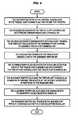
- FIG. 1illustrates a data communication system in the prior art.
- FIG. 2illustrates a data communication circuit in an example of the invention.
- FIG. 3illustrates a data communication system in an example of the invention.
- FIG. 4illustrates the operation of a decoder and alignment buffer in an example of the invention.
- FIG. 5illustrates the operation of a decoder in an example of the invention.
- FIG. 6illustrates the operation of an alignment buffer in an example of the invention.
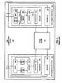
- FIG. 1Prior Art Data Communication System
- FIG. 1illustrates a data communication system 150 in the prior art.
- the data communication system 150includes a data communication circuit 100 coupled to another data communication circuit 120 by an optical communication system 115 .
- the data communication circuit 100includes a transmitter 101 and a receiver 102 .
- the data communication circuit 120includes a transmitter 121 and a receiver 122 .
- the receiver 102is configured and operates like the receiver 122 .
- the transmitter 121is configured and operates like the transmitter 101 .
- the transmitter 101includes a demux 104 , delay 105 , Cyclic Redundancy Check (CRC) 106 , encoder 107 , and serializer 108 .
- the receiver 122includes a de-serializer 123 , decoder 124 , alignment buffer 125 , mux 126 , and CRC 127 .
- the data communication system 150is configured to operate as follows.
- the demux 104receives and processes an optical OC- 192 signal.
- the demux 104includes error correction logic to calculate parity.
- the demux 104transfers eleven parallel channels to both the delay 105 and the CRC 106 . These parallel channels include ten 8-bit data channels and one 8-bit parity channel.
- the demux 104also includes a framer that transfers a control signal to the encoder 107 indicating the start of headers in the parallel channels.
- the CRC 106performs CRC calculations for the eleven parallel channels and transfers a resulting CRC channel to the encoder 107 .
- the delay 105introduces a delay into the eleven parallel channels to allow time for the CRC calculations.
- the delay 105transfers the eleven delayed parallel channels to the encoder 107 .
- the encoder 107receives the control signal and twelve 8-bit parallel channels.
- the twelve 8-bit parallel channelsare comprised of 10 data channels, one parity channel, and one CRC channel.
- the encoder 107converts the twelve 8-bit parallel channels into twelve corresponding 10-bit parallel channels.
- the conversionencodes clocking into the 10-bit parallel channels and removes bias.
- the encoder 107also inserts a control character, such as a comma, to delimit each header in response to the control signal from the demux 104 .
- the encoder 107transfers the twelve 10-bit parallel channels to the serializer 108 .
- the serializer 108converts the twelve 10-bit parallel channels into twelve 1-bit parallel channels.
- the serializer 108transfers the twelve 1-bit parallel channels to the optical system 115 .
- the optical system 115converts the twelve 1-bit channels from electrical to optical and transfers the optical signals toward the data communications circuit 120 . Before transfer to the data communication circuit 120 , the optical system 115 re-converts the optical signals from optical to electrical and recovers clocking.
- the optical system 115transfers twelve 1-bit parallel channels, including twelve recovered clocks, to the de-serializer 123 .
- the de-serializer 123converts the twelve 1-bit channels into twelve 10-bit parallel channels 130 .
- the twelve 10-bit parallel channels 130are comprised of ten data channels, one parity channel, and one CRC channel.
- the de-serializer 123transfers the twelve 10-bit channels 130 to the decoder 124 .
- the decoder 124converts the twelve 10-bit channels 130 into twelve corresponding 8-bit channels 131 .
- the decoder 124transfers the twelve 8-bit channels 131 to the alignment buffer 125 .
- the alignment buffer 125aligns the 8-bit parallel channels 131 in memory by detecting the headers in the twelve 8-bit channels 131 .
- the alignment buffer 125transfers the aligned 8-bit parallel channels 132 to the mux 126 and the CRC 127 .
- the mux 126converts the aligned 8-bit parallel channels 132 into a corresponding OC- 192 signal.
- the mux 126transfers the OC- 192 signal.
- the mux 126includes a protection switch and a polarity switch.
- the mux 126also includes error correction logic to process the parity channel to detect errors and control the polarity switch.
- the CRC 127performs CRC validation for the aligned 8-bit parallel channels 132 .
- the alignment buffer 125may confuse actual user data with the header. The confusion causes false header detection in the alignment buffer 125 that results in channel misalignment and faulty clocking.
- the mux 126 and the CRC 127are unable to effectively process the parallel channels 132 if channel misalignment or faulty clocking are present.
- the data communication system 150fails to effectively transfer the user data.
- FIG. 2illustrates a specific example of a data communication circuit in accord with the present invention.
- FIG. 2illustrates a data communication circuit 220 in an example of the invention.
- the data communication circuit 220includes a decoder 224 coupled to an alignment buffer 225 .
- the following variables (N), (M), and (X)represent integers.
- the decoder 224 and alignment buffer 225are configured to operate as follows.
- the decoderreceives and decodes parallel (N) bit channels 230 into parallel (M+X) bit channels 240 that include signaling bits that indicate headers in the parallel (M+X) bit channels 240 .
- the decodertransfers the parallel (M+X) bit channels 240 to the alignment buffer 225 .
- the alignment buffer 225recovers parallel (M) bit channels 231 and the signaling bits from the parallel (M+X) bit channels 240 .
- the alignment buffer 225aligns the parallel (M) bit channels 231 using the signaling bits.
- the data communication circuit 220has multiple clocks.
- the alignment buffer 225uses the signaling bits to generate a clock selection signal 241 that identifies one of these clocks that is functioning properly. Other components use the properly functioning clock in response to the clock selection signal 241 .
- the alignment buffer 225transfers the aligned parallel (M) bit channels 232 and the clock selection signal 241 .
- the alignment buffer 225has a length that is a multiple of a frame length for the (M) bit parallel channels 231 .
- This buffer lengthhas a wrap-around effect that causes the alignment buffer 225 to write headers at repeating addresses. Repeating header addresses reduce the complexity of the buffer logic.
- the data communication circuit 220has improved channel alignment and clocking.
- the alignment buffer 225uses the signaling bits for channel alignment and clocking instead of trying to detect headers in the user data. As a result, the alignment buffer 225 is prevented from detecting false headers in the user data.
- the signaling bitsavoid the misaligned channels and faulty clocking caused by false header detection.
- FIGS. 3-4illustrate a specific example of a data communication system in accord with the present invention. Those skilled in the art will appreciate numerous variations from this example that do not depart from the scope of the invention. Those skilled in the art will also appreciate that various features described below could be combined with the above-described embodiment to form multiple variations of the invention.
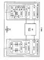
- FIG. 3illustrates a data communication system 350 in an example of the invention.
- the data communication system 350includes a data communication circuit 300 coupled to a data communication circuit 320 by an optical communication system 315 .
- the data communication circuit 300includes a transmitter 301 and a receiver 302 .
- the data communication circuit 320includes a transmitter 321 and a receiver 322 .
- the receiver 302is configured and operates like the receiver 322 .
- the transmitter 321is configured and operates like the transmitter 301 .
- the transmitter 301includes a demux 304 , delay 305 , CRC 306 , encoder 307 , and serializer 308 .
- the receiver 322includes a de-serializer 323 , decoder 324 , alignment buffer 325 , mux 326 , and CRC 327 . Aside from the decoder 324 and the alignment buffer 325 , the configuration and operation of these components and systems could be conventional.
- the data communication system 350is configured to operate as follows.
- the demux 304receives and processes an OC- 192 signal.
- the demux 304includes error correction logic to calculate parity.
- the demux 304transfers eleven parallel channels to both the delay 305 and the CRC 306 . These parallel channels include ten 8-bit data channels and one 8-bit parity channel.
- the demux 304also includes a framer that transfers a control signal to the encoder 307 indicating the start of headers in the parallel channels.
- the CRC 306performs CRC calculations for the eleven parallel channels and transfers a resulting CRC channel to the encoder 307 .
- the delay 305introduces a delay into the eleven parallel channels to allow time for the CRC calculations.
- the delay 305transfers the eleven delayed parallel channels to the encoder 307 .
- the encoder 307receives the control signal and twelve 8-bit parallel channels.
- the twelve 8-bit parallel channelsare comprised of 10 data channels, one parity channel, and one CRC channel.
- the encoder 307converts the twelve 8-bit parallel channels into twelve corresponding 10-bit parallel channels.
- the conversionencodes clocking into the 10-bit parallel channels and removes bias.
- the encoder 307also inserts a control character, such as a comma, to delimit each header in response to the control signal from the demux 304 .
- the encoder 307transfers the twelve 10-bit parallel channels to the serializer 308 .
- the serializer 308converts the twelve 10-bit parallel channels into twelve 1-bit parallel channels.
- the serializer 308transfers the twelve 1-bit parallel channels to the optical system 315 .
- the optical system 315converts the twelve 1-bit channels from electrical to optical and transfers the optical signals toward the data communications circuit 320 . Before transfer to the data communication circuit 320 , the optical system 315 re-converts the optical signals from optical to electrical and recovers clocking. If desired, the clock data recovery circuitry that recovers the clocking could be integrated into the data communication circuit 320 .
- the optical system 315transfers twelve 1-bit parallel channels, including twelve recovered clocks, to the de-serializer 323 .
- the de-serializer 323converts the twelve 1-bit channels into twelve 10-bit parallel channels 330 .
- the twelve 10-bit parallel channels 330are comprised of ten data channels, one parity channel, and one CRC channel.
- the de-serializer 323transfers the twelve 10-bit channels 330 to the decoder 324 .
- FIG. 4depicts the operation of the decoder 324 and the alignment buffer 325 in an example of the invention.
- the decoder 324detects the control characters in the twelve 10-bit channels 330 that delimit the headers.
- the decoder 324converts the twelve 10-bit channels 330 into twelve corresponding 8-bit channels 331 .
- the decoder 324Based on the control character detection, the decoder 324 generates signaling bits for each of the 8-bit channels 331 that indicate the location of the headers in each 8-bit channel.
- the decoder 324inserts the signaling bits into the twelve 8-bit channels 331 to generate twelve 9-bit channels 340 .
- the signaling bitsare controlled so each channel includes signaling bits that indicate the start of headers in that channel.
- the decoder 324transfers the twelve 9-bit channels 340 to the alignment buffer 325 .
- the alignment buffer 325recovers the signaling bits from each of the twelve 9-bit channels 340 .
- the alignment buffer 325converts the twelve 9-bit channels into the twelve 8-bit channels 331 .
- the alignment buffer 325writes the twelve 8-bit channels 331 to internal memory space.
- the alignment buffer 325begins writing the 8-bit parallel channels 331 to specific addresses when the signaling bits indicate a header is present. Thus, the headers are aligned at the specific addresses.
- the alignment buffer 325has a length that is a multiple of the frame length for the 8-bit bit parallel channels 331 . This buffer length creates a wrap-around effect that causes the alignment buffer 325 to write headers at repeating addresses. A repeating header address is typically located at the beginning of the memory space and reduces the complexity of the buffer logic.
- the alignment buffer 325transfers the aligned 8-bit parallel channels 332 to the mux 326 and the CRC 327 .
- the alignment buffer 325also uses the signaling bits to generate a clock selection signal 341 .
- the timing skew across channelsis 100 nanoseconds so the clock, which is derived from one channel, will provide accurate timing for the other parallel channels. If the channel used for the clock malfunctions, then the alignment buffer 325 changes the clock selection signal 341 to identify a clock from a properly functioning channel.
- the alignment buffer 325transfers clock selection signal 341 to clock selection circuitry (not shown).
- the mux 326converts the aligned 8-bit parallel channels 332 into a corresponding OC- 192 signal.
- the mux 326transfers the OC- 192 signal.
- the mux 326includes a protection switch and a polarity switch.
- the mux 326also includes error correction logic to process the parity channel to detect errors and control the polarity switch.
- the CRC 327performs CRC validation for the aligned 8-bit parallel channels 332 .
- FIGS. 5-6illustrate a specific example of a decoder and alignment buffer in accord with the present invention. Those skilled in the art will appreciate numerous variations from this example that do not depart from the scope of the invention. Those skilled in the art will also appreciate that various features described below could be combined with the above-described embodiments to form multiple variations of the invention.
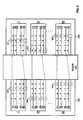
- FIG. 5illustrates the operation of a decoder 524 in an example of the invention.
- the decoderreceives twelve 10-bit parallel channels 530 .
- the channel and bit designationsare indicated in boxes at the left, and for clarity, all of the channels and bits are not shown.
- the first channelincludes a control character 551 at the start of a header.
- the control character 551is represented by all “1” bits, but typically, the control character is the bit pattern of a comma character.
- the second and twelfth channelsrespectively include control characters 552 and 553 at the start of headers. Note that the control characters 551 - 553 and associated headers and channels are not aligned.
- the right side of FIG. 5depicts the same information from the twelve 10-bit parallel channels 530 after processing by the decoder 524 to generate the resulting twelve 9-bit parallel channels 540 .
- the decoder 524decodes the 10-bit channels 530 into the first 8 bits of the 9-bit channels 540 to remove the encoding of the transmitter 301 . Note that decoding converts the control characters 551 - 553 from all “1”s to all “0”s and changes other bits as well.
- the decoder 524adds a ninth bit to the 9-bit channels 540 to identify the position of the control characters 551 - 553 . A “1” bit is placed in the ninth bit of each channel at the same position as the control character in that channel. Otherwise, the ninth bit is a “0”. Note that the control characters 551 - 553 and associated headers and channels are still not aligned.
- FIG. 6depicts the operation of the alignment buffer 625 in an example of the invention.
- the alignment buffer 625includes memory space that has a first address 661 and a last address 664 .
- the second and twelfth channelsalso have their respective first addresses 662 - 663 and last addresses 665 - 666 .
- the alignment buffer 625receives the twelve 9-bit channels 540 from the decoder 524 of FIG. 5 .
- the alignment bufferdetects a “1” in the ninth bit of one of the 9-bit channels 540 , it starts writing data from that channel to the first address in the memory space for that channel.
- This techniquealigns the start of the headers for all of the parallel channels at the first addresses 661 - 663 . Since the alignment buffer has a length that is a multiple of the frame length, the last bits before the header occupy the last addresses 664 - 666 .
- the bits 1 - 8 before the control character 552are also all “0”s just like a decoded control character. If the alignment buffer 625 were looking at the bits 1 - 8 , it might misinterpret these “0”s as the control character 552 and misalign the channels. Instead, the alignment buffer 625 looks at the ninth bit which has a “1” identifying the control character 552 , but a “0” everywhere else. Thus, the header signaling in the ninth bit avoids false header detection.
- the alignment buffer 625When the alignment buffer 625 receives a “1” in the ninth bit for all of the 9-bit parallel channels 540 , it begins to read the channels at the first addresses 661 - 663 in the memory space to generate the 8-bit parallel channels 632 . Note that the control characters 551 - 553 and the associated headers and channels are now aligned.
Landscapes
- Engineering & Computer Science (AREA)
- Computer Networks & Wireless Communication (AREA)
- Signal Processing (AREA)
- Power Engineering (AREA)
- Detection And Prevention Of Errors In Transmission (AREA)
Abstract
Description
Claims (46)
Priority Applications (1)
| Application Number | Priority Date | Filing Date | Title |
|---|---|---|---|
| US09/487,139US6829315B1 (en) | 2000-01-19 | 2000-01-19 | Alignment of parallel data channels using header detection signaling |
Applications Claiming Priority (1)
| Application Number | Priority Date | Filing Date | Title |
|---|---|---|---|
| US09/487,139US6829315B1 (en) | 2000-01-19 | 2000-01-19 | Alignment of parallel data channels using header detection signaling |
Publications (1)
| Publication Number | Publication Date |
|---|---|
| US6829315B1true US6829315B1 (en) | 2004-12-07 |
Family
ID=33477002
Family Applications (1)
| Application Number | Title | Priority Date | Filing Date |
|---|---|---|---|
| US09/487,139Expired - LifetimeUS6829315B1 (en) | 2000-01-19 | 2000-01-19 | Alignment of parallel data channels using header detection signaling |
Country Status (1)
| Country | Link |
|---|---|
| US (1) | US6829315B1 (en) |
Cited By (11)
| Publication number | Priority date | Publication date | Assignee | Title |
|---|---|---|---|---|
| US20030091039A1 (en)* | 2001-11-15 | 2003-05-15 | International Business Machines Corporation | Modification of bus protocol packet for serial data synchronization |
| US20050149725A1 (en)* | 2003-12-30 | 2005-07-07 | Intel Corporation | Method and apparatus for aligning ciphered data |
| US20050149744A1 (en)* | 2003-12-29 | 2005-07-07 | Intel Corporation | Network processor having cryptographic processing including an authentication buffer |
| US20070006053A1 (en)* | 2005-07-01 | 2007-01-04 | Lucent Technologies Inc. | Method and apparatus for synchronizing data channels using an alternating parity deskew channel |
| US7277031B1 (en)* | 2003-12-15 | 2007-10-02 | Marvell International Ltd. | 100Base-FX serializer/deserializer using 10000Base-X serializer/deserializer |
| US20070291735A1 (en)* | 2005-12-28 | 2007-12-20 | Lucent Technologies Inc. | Method and apparatus for temporal alignment of multiple parallel data streams |
| US20080288848A1 (en)* | 2007-05-15 | 2008-11-20 | Intel Corporation | Latency by offsetting cyclic redundancy code lanes from data lanes |
| US7512945B2 (en) | 2003-12-29 | 2009-03-31 | Intel Corporation | Method and apparatus for scheduling the processing of commands for execution by cryptographic algorithm cores in a programmable network processor |
| US20090246907A1 (en)* | 2007-08-13 | 2009-10-01 | Unitel Solar Ovonic Llc | Higher Selectivity, Method for passivating short circuit current paths in semiconductor devices |
| US8041945B2 (en) | 2003-12-19 | 2011-10-18 | Intel Corporation | Method and apparatus for performing an authentication after cipher operation in a network processor |
| CN105049145A (en)* | 2015-06-15 | 2015-11-11 | 哈尔滨工业大学 | Frame header rapid synchronization system and method |
Citations (11)
| Publication number | Priority date | Publication date | Assignee | Title |
|---|---|---|---|---|
| US4486739A (en) | 1982-06-30 | 1984-12-04 | International Business Machines Corporation | Byte oriented DC balanced (0,4) 8B/10B partitioned block transmission code |
| US4701913A (en)* | 1986-06-11 | 1987-10-20 | Northern Telecom Limited | Circuit and method for extracting signalling information embedded in channelized serial data streams |
| US4967405A (en) | 1988-12-09 | 1990-10-30 | Transwitch Corporation | System for cross-connecting high speed digital SONET signals |
| US5025458A (en)* | 1989-10-30 | 1991-06-18 | International Business Machines Corporation | Apparatus for decoding frames from a data link |
| US5113395A (en)* | 1989-09-14 | 1992-05-12 | Nec Corporation | Frame phase aligning system using a buffer memory with a reduced capacity |
| US5408473A (en)* | 1992-03-03 | 1995-04-18 | Digital Equipment Corporation | Method and apparatus for transmission of communication signals over two parallel channels |
| US5598442A (en) | 1994-06-17 | 1997-01-28 | International Business Machines Corporation | Self-timed parallel inter-system data communication channel |
| US5861825A (en)* | 1996-03-21 | 1999-01-19 | Sony Corporation | Method and device for code modulation, method and device for code demodulation, and method and device for decoding |
| US6201829B1 (en)* | 1998-04-03 | 2001-03-13 | Adaptec, Inc. | Serial/parallel GHZ transceiver with pseudo-random built in self test pattern generator |
| US6233073B1 (en)* | 1998-07-30 | 2001-05-15 | International Business Machines Corporation | Diagnostic injection of transmission errors in fiber optic networks |
| US6362757B1 (en)* | 1999-08-20 | 2002-03-26 | Electronics And Telecommunications Research Institute | Method and apparatus for encoding MB810 line code with the characteristics of minimum bandwidth and DC-free |
- 2000
- 2000-01-19USUS09/487,139patent/US6829315B1/ennot_activeExpired - Lifetime
Patent Citations (11)
| Publication number | Priority date | Publication date | Assignee | Title |
|---|---|---|---|---|
| US4486739A (en) | 1982-06-30 | 1984-12-04 | International Business Machines Corporation | Byte oriented DC balanced (0,4) 8B/10B partitioned block transmission code |
| US4701913A (en)* | 1986-06-11 | 1987-10-20 | Northern Telecom Limited | Circuit and method for extracting signalling information embedded in channelized serial data streams |
| US4967405A (en) | 1988-12-09 | 1990-10-30 | Transwitch Corporation | System for cross-connecting high speed digital SONET signals |
| US5113395A (en)* | 1989-09-14 | 1992-05-12 | Nec Corporation | Frame phase aligning system using a buffer memory with a reduced capacity |
| US5025458A (en)* | 1989-10-30 | 1991-06-18 | International Business Machines Corporation | Apparatus for decoding frames from a data link |
| US5408473A (en)* | 1992-03-03 | 1995-04-18 | Digital Equipment Corporation | Method and apparatus for transmission of communication signals over two parallel channels |
| US5598442A (en) | 1994-06-17 | 1997-01-28 | International Business Machines Corporation | Self-timed parallel inter-system data communication channel |
| US5861825A (en)* | 1996-03-21 | 1999-01-19 | Sony Corporation | Method and device for code modulation, method and device for code demodulation, and method and device for decoding |
| US6201829B1 (en)* | 1998-04-03 | 2001-03-13 | Adaptec, Inc. | Serial/parallel GHZ transceiver with pseudo-random built in self test pattern generator |
| US6233073B1 (en)* | 1998-07-30 | 2001-05-15 | International Business Machines Corporation | Diagnostic injection of transmission errors in fiber optic networks |
| US6362757B1 (en)* | 1999-08-20 | 2002-03-26 | Electronics And Telecommunications Research Institute | Method and apparatus for encoding MB810 line code with the characteristics of minimum bandwidth and DC-free |
Non-Patent Citations (2)
| Title |
|---|
| Nowell, Mark, "Proposal for a very Short Reach (VSR) OC-192/STM-64 Interface Based on Parallel Optics," Working Group: Physical and Link Layer (PLL), pp. ten, (Oct. 19-20, 1999 OIF meeting, Los Angeles). |
| Stugrin, Michael, "Conexant Works with Cisco to Define Interconnection Standard that Cuts Costs of Depolying High-Speed Wide Area Networks," Internet, Conexant, No. 1, p. two, (Nov. 10, 1999). |
Cited By (24)
| Publication number | Priority date | Publication date | Assignee | Title |
|---|---|---|---|---|
| US7065101B2 (en)* | 2001-11-15 | 2006-06-20 | International Business Machines Corporation | Modification of bus protocol packet for serial data synchronization |
| US20030091039A1 (en)* | 2001-11-15 | 2003-05-15 | International Business Machines Corporation | Modification of bus protocol packet for serial data synchronization |
| US7994950B1 (en) | 2003-12-15 | 2011-08-09 | Marvell International Ltd. | 100BASE-FX serializer/deserializer using 1000BASE-X serializer/deserializer |
| US7277031B1 (en)* | 2003-12-15 | 2007-10-02 | Marvell International Ltd. | 100Base-FX serializer/deserializer using 10000Base-X serializer/deserializer |
| US7791512B1 (en) | 2003-12-15 | 2010-09-07 | Marvell International Ltd. | 100Base-FX serializer/deserializer using 1000Base-X serializer/deserializer |
| US7477172B1 (en) | 2003-12-15 | 2009-01-13 | Marvell International Ltd. | 100base-FX serializer/deserializer using 1000base-X serializer/deserializer |
| US8417943B2 (en) | 2003-12-19 | 2013-04-09 | Intel Corporation | Method and apparatus for performing an authentication after cipher operation in a network processor |
| US8041945B2 (en) | 2003-12-19 | 2011-10-18 | Intel Corporation | Method and apparatus for performing an authentication after cipher operation in a network processor |
| US20050149744A1 (en)* | 2003-12-29 | 2005-07-07 | Intel Corporation | Network processor having cryptographic processing including an authentication buffer |
| US8065678B2 (en) | 2003-12-29 | 2011-11-22 | Intel Corporation | Method and apparatus for scheduling the processing of commands for execution by cryptographic algorithm cores in a programmable network processor |
| US7512945B2 (en) | 2003-12-29 | 2009-03-31 | Intel Corporation | Method and apparatus for scheduling the processing of commands for execution by cryptographic algorithm cores in a programmable network processor |
| US20050149725A1 (en)* | 2003-12-30 | 2005-07-07 | Intel Corporation | Method and apparatus for aligning ciphered data |
| US7529924B2 (en)* | 2003-12-30 | 2009-05-05 | Intel Corporation | Method and apparatus for aligning ciphered data |
| US7467335B2 (en) | 2005-07-01 | 2008-12-16 | Alcatel-Lucent Usa Inc. | Method and apparatus for synchronizing data channels using an alternating parity deskew channel |
| WO2007005686A1 (en)* | 2005-07-01 | 2007-01-11 | Lucent Technologies Inc. | Method and apparatus for synchronizing data channels using deskew channel |
| US20070006053A1 (en)* | 2005-07-01 | 2007-01-04 | Lucent Technologies Inc. | Method and apparatus for synchronizing data channels using an alternating parity deskew channel |
| US7613125B2 (en)* | 2005-12-28 | 2009-11-03 | Alcatel-Lucent Usa Inc. | Method and apparatus for temporal alignment of multiple parallel data streams |
| US20070291735A1 (en)* | 2005-12-28 | 2007-12-20 | Lucent Technologies Inc. | Method and apparatus for temporal alignment of multiple parallel data streams |
| CN101325090A (en)* | 2007-05-15 | 2008-12-17 | 英特尔公司 | Offsetting cyclic redundancy code lanes from data lanes to reduce latency |
| US7644344B2 (en)* | 2007-05-15 | 2010-01-05 | Intel Corporation | Latency by offsetting cyclic redundancy code lanes from data lanes |
| US20080288848A1 (en)* | 2007-05-15 | 2008-11-20 | Intel Corporation | Latency by offsetting cyclic redundancy code lanes from data lanes |
| US20090246907A1 (en)* | 2007-08-13 | 2009-10-01 | Unitel Solar Ovonic Llc | Higher Selectivity, Method for passivating short circuit current paths in semiconductor devices |
| CN105049145A (en)* | 2015-06-15 | 2015-11-11 | 哈尔滨工业大学 | Frame header rapid synchronization system and method |
| CN105049145B (en)* | 2015-06-15 | 2017-09-26 | 哈尔滨工业大学 | frame head fast synchronization system and method |
Similar Documents
| Publication | Publication Date | Title |
|---|---|---|
| JP2694807B2 (en) | Data transmission method | |
| US6650638B1 (en) | Decoding method and decoder for 64b/66b coded packetized serial data | |
| US7738601B2 (en) | Coding and decoding packetized data | |
| US9118392B2 (en) | Isolated serializer-deserializer | |
| US8259760B2 (en) | Apparatus and method for transmitting and recovering multi-lane encoded data streams using a reduced number of lanes | |
| US6829315B1 (en) | Alignment of parallel data channels using header detection signaling | |
| US7499516B2 (en) | Methods and apparatus for interface buffer management and clock compensation in data transfers | |
| US20040150537A1 (en) | Transmitting data words | |
| JP2007502570A (en) | Automatic realignment of multiple serial byte lanes | |
| US9479277B2 (en) | Mechanism for channel synchronization | |
| EP1320208A2 (en) | Serial communications system and method | |
| JP2648752B2 (en) | Device that guarantees accurate decoding of data information | |
| KR100513275B1 (en) | A data recovery algorithm using data position detecting and a serial data receiver adopting the algorithm | |
| US5428611A (en) | Strong framing protocol for HDLC and other run-length codes | |
| EP0448045B1 (en) | System for suppressing spread of error generated in differential coding | |
| US8972828B1 (en) | High speed interconnect protocol and method | |
| US5093830A (en) | Self-synchronizing serial transmission of signaling bits in a digital switch | |
| JPS61292434A (en) | Buffer memory | |
| US6895542B2 (en) | Data recovery circuit and method and data receiving system using the same | |
| JP3268337B2 (en) | Line switching method | |
| WO2005004378A1 (en) | An intelligent universal calibration logic in embedded high speed transceiver (serdes) applications | |
| JPS63306729A (en) | clock switching circuit | |
| JP3202379B2 (en) | Packet frame transmission method | |
| JP2658927B2 (en) | Multiplex transmission method and apparatus | |
| US20030061374A1 (en) | Multiplexing high priority, low bandwidth information on a traditional link protocol |
Legal Events
| Date | Code | Title | Description |
|---|---|---|---|
| AS | Assignment | Owner name:CONEXANT SYSTEMS, INC., CALIFORNIA Free format text:ASSIGNMENT OF ASSIGNORS INTEREST;ASSIGNOR:CRUIKSHANK, BRIAN;REEL/FRAME:010521/0463 Effective date:20000119 | |
| AS | Assignment | Owner name:MINDSPEED TECHNOLOGIES, INC., CALIFORNIA Free format text:ASSIGNMENT OF ASSIGNORS INTEREST;ASSIGNOR:CONEXANT SYSTEMS, INC.;REEL/FRAME:014568/0275 Effective date:20030627 | |
| AS | Assignment | Owner name:CONEXANT SYSTEMS, INC., CALIFORNIA Free format text:SECURITY AGREEMENT;ASSIGNOR:MINDSPEED TECHNOLOGIES, INC.;REEL/FRAME:014546/0305 Effective date:20030930 | |
| FEPP | Fee payment procedure | Free format text:PAYOR NUMBER ASSIGNED (ORIGINAL EVENT CODE: ASPN); ENTITY STATUS OF PATENT OWNER: LARGE ENTITY | |
| STCF | Information on status: patent grant | Free format text:PATENTED CASE | |
| FPAY | Fee payment | Year of fee payment:4 | |
| FEPP | Fee payment procedure | Free format text:PAYOR NUMBER ASSIGNED (ORIGINAL EVENT CODE: ASPN); ENTITY STATUS OF PATENT OWNER: LARGE ENTITY Free format text:PAYER NUMBER DE-ASSIGNED (ORIGINAL EVENT CODE: RMPN); ENTITY STATUS OF PATENT OWNER: LARGE ENTITY | |
| FPAY | Fee payment | Year of fee payment:8 | |
| AS | Assignment | Owner name:MINDSPEED TECHNOLOGIES, INC, CALIFORNIA Free format text:RELEASE OF SECURITY INTEREST;ASSIGNOR:CONEXANT SYSTEMS, INC;REEL/FRAME:031494/0937 Effective date:20041208 | |
| AS | Assignment | Owner name:JPMORGAN CHASE BANK, N.A., AS ADMINISTRATIVE AGENT Free format text:SECURITY INTEREST;ASSIGNOR:MINDSPEED TECHNOLOGIES, INC.;REEL/FRAME:032495/0177 Effective date:20140318 | |
| AS | Assignment | Owner name:GOLDMAN SACHS BANK USA, NEW YORK Free format text:SECURITY INTEREST;ASSIGNORS:M/A-COM TECHNOLOGY SOLUTIONS HOLDINGS, INC.;MINDSPEED TECHNOLOGIES, INC.;BROOKTREE CORPORATION;REEL/FRAME:032859/0374 Effective date:20140508 Owner name:MINDSPEED TECHNOLOGIES, INC., CALIFORNIA Free format text:RELEASE BY SECURED PARTY;ASSIGNOR:JPMORGAN CHASE BANK, N.A.;REEL/FRAME:032861/0617 Effective date:20140508 | |
| FPAY | Fee payment | Year of fee payment:12 | |
| AS | Assignment | Owner name:MINDSPEED TECHNOLOGIES, LLC, MASSACHUSETTS Free format text:CHANGE OF NAME;ASSIGNOR:MINDSPEED TECHNOLOGIES, INC.;REEL/FRAME:039645/0264 Effective date:20160725 | |
| AS | Assignment | Owner name:MACOM TECHNOLOGY SOLUTIONS HOLDINGS, INC., MASSACH Free format text:ASSIGNMENT OF ASSIGNORS INTEREST;ASSIGNOR:MINDSPEED TECHNOLOGIES, LLC;REEL/FRAME:044791/0600 Effective date:20171017 |