US6828674B2 - Hermetically sealed microstructure package - Google Patents
Hermetically sealed microstructure packageDownload PDFInfo
- Publication number
- US6828674B2 US6828674B2US10/164,064US16406402AUS6828674B2US 6828674 B2US6828674 B2US 6828674B2US 16406402 AUS16406402 AUS 16406402AUS 6828674 B2US6828674 B2US 6828674B2
- Authority
- US
- United States
- Prior art keywords
- microstructure
- substrate
- microstructures
- circuitry
- wafer
- Prior art date
- Legal status (The legal status is an assumption and is not a legal conclusion. Google has not performed a legal analysis and makes no representation as to the accuracy of the status listed.)
- Expired - Lifetime
Links
Images


Classifications
- B—PERFORMING OPERATIONS; TRANSPORTING
- B81—MICROSTRUCTURAL TECHNOLOGY
- B81B—MICROSTRUCTURAL DEVICES OR SYSTEMS, e.g. MICROMECHANICAL DEVICES
- B81B7/00—Microstructural systems; Auxiliary parts of microstructural devices or systems
- B81B7/0032—Packages or encapsulation
- B81B7/007—Interconnections between the MEMS and external electrical signals
- B—PERFORMING OPERATIONS; TRANSPORTING
- B81—MICROSTRUCTURAL TECHNOLOGY
- B81C—PROCESSES OR APPARATUS SPECIALLY ADAPTED FOR THE MANUFACTURE OR TREATMENT OF MICROSTRUCTURAL DEVICES OR SYSTEMS
- B81C1/00—Manufacture or treatment of devices or systems in or on a substrate
- B81C1/00349—Creating layers of material on a substrate
- B81C1/00357—Creating layers of material on a substrate involving bonding one or several substrates on a non-temporary support, e.g. another substrate
- H—ELECTRICITY
- H01—ELECTRIC ELEMENTS
- H01L—SEMICONDUCTOR DEVICES NOT COVERED BY CLASS H10
- H01L23/00—Details of semiconductor or other solid state devices
- H01L23/02—Containers; Seals
- H01L23/10—Containers; Seals characterised by the material or arrangement of seals between parts, e.g. between cap and base of the container or between leads and walls of the container
- B—PERFORMING OPERATIONS; TRANSPORTING
- B81—MICROSTRUCTURAL TECHNOLOGY
- B81C—PROCESSES OR APPARATUS SPECIALLY ADAPTED FOR THE MANUFACTURE OR TREATMENT OF MICROSTRUCTURAL DEVICES OR SYSTEMS
- B81C2201/00—Manufacture or treatment of microstructural devices or systems
- B81C2201/01—Manufacture or treatment of microstructural devices or systems in or on a substrate
- B81C2201/0174—Manufacture or treatment of microstructural devices or systems in or on a substrate for making multi-layered devices, film deposition or growing
- B81C2201/019—Bonding or gluing multiple substrate layers
- H—ELECTRICITY
- H01—ELECTRIC ELEMENTS
- H01L—SEMICONDUCTOR DEVICES NOT COVERED BY CLASS H10
- H01L2224/00—Indexing scheme for arrangements for connecting or disconnecting semiconductor or solid-state bodies and methods related thereto as covered by H01L24/00
- H01L2224/01—Means for bonding being attached to, or being formed on, the surface to be connected, e.g. chip-to-package, die-attach, "first-level" interconnects; Manufacturing methods related thereto
- H01L2224/02—Bonding areas; Manufacturing methods related thereto
- H01L2224/04—Structure, shape, material or disposition of the bonding areas prior to the connecting process
- H01L2224/05—Structure, shape, material or disposition of the bonding areas prior to the connecting process of an individual bonding area
- H01L2224/0554—External layer
- H01L2224/05599—Material
- H—ELECTRICITY
- H01—ELECTRIC ELEMENTS
- H01L—SEMICONDUCTOR DEVICES NOT COVERED BY CLASS H10
- H01L2224/00—Indexing scheme for arrangements for connecting or disconnecting semiconductor or solid-state bodies and methods related thereto as covered by H01L24/00
- H01L2224/01—Means for bonding being attached to, or being formed on, the surface to be connected, e.g. chip-to-package, die-attach, "first-level" interconnects; Manufacturing methods related thereto
- H01L2224/42—Wire connectors; Manufacturing methods related thereto
- H01L2224/44—Structure, shape, material or disposition of the wire connectors prior to the connecting process
- H01L2224/45—Structure, shape, material or disposition of the wire connectors prior to the connecting process of an individual wire connector
- H01L2224/45001—Core members of the connector
- H01L2224/45099—Material
- H01L2224/451—Material with a principal constituent of the material being a metal or a metalloid, e.g. boron (B), silicon (Si), germanium (Ge), arsenic (As), antimony (Sb), tellurium (Te) and polonium (Po), and alloys thereof
- H01L2224/45117—Material with a principal constituent of the material being a metal or a metalloid, e.g. boron (B), silicon (Si), germanium (Ge), arsenic (As), antimony (Sb), tellurium (Te) and polonium (Po), and alloys thereof the principal constituent melting at a temperature of greater than or equal to 400°C and less than 950°C
- H01L2224/45124—Aluminium (Al) as principal constituent
- H—ELECTRICITY
- H01—ELECTRIC ELEMENTS
- H01L—SEMICONDUCTOR DEVICES NOT COVERED BY CLASS H10
- H01L2224/00—Indexing scheme for arrangements for connecting or disconnecting semiconductor or solid-state bodies and methods related thereto as covered by H01L24/00
- H01L2224/01—Means for bonding being attached to, or being formed on, the surface to be connected, e.g. chip-to-package, die-attach, "first-level" interconnects; Manufacturing methods related thereto
- H01L2224/42—Wire connectors; Manufacturing methods related thereto
- H01L2224/44—Structure, shape, material or disposition of the wire connectors prior to the connecting process
- H01L2224/45—Structure, shape, material or disposition of the wire connectors prior to the connecting process of an individual wire connector
- H01L2224/45001—Core members of the connector
- H01L2224/45099—Material
- H01L2224/451—Material with a principal constituent of the material being a metal or a metalloid, e.g. boron (B), silicon (Si), germanium (Ge), arsenic (As), antimony (Sb), tellurium (Te) and polonium (Po), and alloys thereof
- H01L2224/45138—Material with a principal constituent of the material being a metal or a metalloid, e.g. boron (B), silicon (Si), germanium (Ge), arsenic (As), antimony (Sb), tellurium (Te) and polonium (Po), and alloys thereof the principal constituent melting at a temperature of greater than or equal to 950°C and less than 1550°C
- H01L2224/45144—Gold (Au) as principal constituent
- H—ELECTRICITY
- H01—ELECTRIC ELEMENTS
- H01L—SEMICONDUCTOR DEVICES NOT COVERED BY CLASS H10
- H01L2224/00—Indexing scheme for arrangements for connecting or disconnecting semiconductor or solid-state bodies and methods related thereto as covered by H01L24/00
- H01L2224/01—Means for bonding being attached to, or being formed on, the surface to be connected, e.g. chip-to-package, die-attach, "first-level" interconnects; Manufacturing methods related thereto
- H01L2224/42—Wire connectors; Manufacturing methods related thereto
- H01L2224/47—Structure, shape, material or disposition of the wire connectors after the connecting process
- H01L2224/48—Structure, shape, material or disposition of the wire connectors after the connecting process of an individual wire connector
- H01L2224/4805—Shape
- H01L2224/4809—Loop shape
- H01L2224/48091—Arched
- H—ELECTRICITY
- H01—ELECTRIC ELEMENTS
- H01L—SEMICONDUCTOR DEVICES NOT COVERED BY CLASS H10
- H01L2224/00—Indexing scheme for arrangements for connecting or disconnecting semiconductor or solid-state bodies and methods related thereto as covered by H01L24/00
- H01L2224/80—Methods for connecting semiconductor or other solid state bodies using means for bonding being attached to, or being formed on, the surface to be connected
- H01L2224/85—Methods for connecting semiconductor or other solid state bodies using means for bonding being attached to, or being formed on, the surface to be connected using a wire connector
- H01L2224/8538—Bonding interfaces outside the semiconductor or solid-state body
- H01L2224/85399—Material
- H—ELECTRICITY
- H01—ELECTRIC ELEMENTS
- H01L—SEMICONDUCTOR DEVICES NOT COVERED BY CLASS H10
- H01L24/00—Arrangements for connecting or disconnecting semiconductor or solid-state bodies; Methods or apparatus related thereto
- H01L24/01—Means for bonding being attached to, or being formed on, the surface to be connected, e.g. chip-to-package, die-attach, "first-level" interconnects; Manufacturing methods related thereto
- H01L24/42—Wire connectors; Manufacturing methods related thereto
- H01L24/44—Structure, shape, material or disposition of the wire connectors prior to the connecting process
- H01L24/45—Structure, shape, material or disposition of the wire connectors prior to the connecting process of an individual wire connector
- H—ELECTRICITY
- H01—ELECTRIC ELEMENTS
- H01L—SEMICONDUCTOR DEVICES NOT COVERED BY CLASS H10
- H01L24/00—Arrangements for connecting or disconnecting semiconductor or solid-state bodies; Methods or apparatus related thereto
- H01L24/01—Means for bonding being attached to, or being formed on, the surface to be connected, e.g. chip-to-package, die-attach, "first-level" interconnects; Manufacturing methods related thereto
- H01L24/42—Wire connectors; Manufacturing methods related thereto
- H01L24/47—Structure, shape, material or disposition of the wire connectors after the connecting process
- H01L24/48—Structure, shape, material or disposition of the wire connectors after the connecting process of an individual wire connector
- H—ELECTRICITY
- H01—ELECTRIC ELEMENTS
- H01L—SEMICONDUCTOR DEVICES NOT COVERED BY CLASS H10
- H01L2924/00—Indexing scheme for arrangements or methods for connecting or disconnecting semiconductor or solid-state bodies as covered by H01L24/00
- H01L2924/0001—Technical content checked by a classifier
- H01L2924/00014—Technical content checked by a classifier the subject-matter covered by the group, the symbol of which is combined with the symbol of this group, being disclosed without further technical details
- H—ELECTRICITY
- H01—ELECTRIC ELEMENTS
- H01L—SEMICONDUCTOR DEVICES NOT COVERED BY CLASS H10
- H01L2924/00—Indexing scheme for arrangements or methods for connecting or disconnecting semiconductor or solid-state bodies as covered by H01L24/00
- H01L2924/01—Chemical elements
- H01L2924/01079—Gold [Au]
- H—ELECTRICITY
- H01—ELECTRIC ELEMENTS
- H01L—SEMICONDUCTOR DEVICES NOT COVERED BY CLASS H10
- H01L2924/00—Indexing scheme for arrangements or methods for connecting or disconnecting semiconductor or solid-state bodies as covered by H01L24/00
- H01L2924/15—Details of package parts other than the semiconductor or other solid state devices to be connected
- H01L2924/161—Cap
- H01L2924/162—Disposition
- H01L2924/16235—Connecting to a semiconductor or solid-state bodies, i.e. cap-to-chip
- H—ELECTRICITY
- H01—ELECTRIC ELEMENTS
- H01L—SEMICONDUCTOR DEVICES NOT COVERED BY CLASS H10
- H01L2924/00—Indexing scheme for arrangements or methods for connecting or disconnecting semiconductor or solid-state bodies as covered by H01L24/00
- H01L2924/15—Details of package parts other than the semiconductor or other solid state devices to be connected
- H01L2924/181—Encapsulation
Definitions
- the present inventionrelates to semiconductor devices, and more particularly, to a protective cover arrangement for a semiconductor substrate containing micro-mechanical devices, wherein the cover arrangement offers more desirable protection and manufacturing characteristics.
- a variety of semiconductor devicesmay be formed on a substrate according to several known techniques.
- the semiconductor devicesmay perform, for examples, electrical, mechanical, optical, or other functions, or combinations of such functions.
- a semiconductor waferserves as a substrate for such devices.
- the devicesmay be fabricated from the semiconductor material of the substrate wafer itself using a variety of known processes, such as growth of various material layers on a surface of the substrate, ion implantation, diffusion, oxidation, photolithography, etching and many other processes.
- During fabricationtypically, at least some portion of each device is formed “within” the substrate wafer, below the surface of the substrate, and may additionally include particular topographic or structural features on the substrate surface.
- semiconductor devicesmay be fabricated from a first semiconductor wafer, and subsequently mounted on a second semiconductor wafer or other type of material that serves as a substrate.
- the semiconductor devices fabricated from the first wafermay be mounted on the substrate either as individual devices or groups of devices. In this case, the devices “reside on” the substrate, as opposed to being “fabricated from” the substrate, as discussed above.
- a device substratemay include one or a large number of devices.
- Functional defectsmay result from one or more environmental hazards, as discussed above, and are a major cause of low device yield and other malperformance characteristics.
- Device damage due to any number of such hazardsmay occur, for example, during the process of “dicing” (separating the device substrate into individual devices), as well as during packaging of devices. Often, the number of functioning devices remaining after dicing and packaging is markedly reduced due to defects resulting from environmental hazards.
- One of these techniquesincludes bonding a protective semiconductor cap wafer to a device substrate before dicing the substrate into individual devices. This technique has been employed particularly with wafer substrates of semiconductor devices that include micro-machined parts or microscopic mechanisms fabricated on the surface of the substrate, such as micro-electrical-mechanical systems, or MEMS. These devices are also referred to as microstructures.
- an entire device substrate waferis capped with another wafer using a pattern of glass-like posts called “frit glass” as a bonding agent.
- the micro-mechanical devicesare hermetically sealed inside an open cavity formed by the frit glass pattern, the device substrate and the cap wafer.
- Hermetic sealingrefers to a particular standard for sealing that is known in the art. Accordingly, any micro-mechanisms are free to move within a cavity while simultaneously being protected from various environmental hazards, such as particulate contamination.
- the cap waferis typically another semiconductor wafer of the same type as that used for the device substrate (for example, silicon or gallium arsenide).
- the cap waferhas essentially identical thermal characteristics to that of the device substrate.
- Such a choice of cap waferresults in avoiding most mechanical stresses that may result from a thermal mismatch between the cap wafer and the device substrate. For example, extreme mechanical stress can occur during a high temperature heat treatment necessary to ensure adequate bonding of the frit glass to the cap wafer and the device substrate. Any mechanical stress can severely damage or even destroy the devices on the substrate, and usually would degrade the accuracy of many delicate micro-machined devices, such as microscopic mechanical sensors or other MEMS.
- the individual devicesAfter the micro-mechanism has been protected by wafer capping, the individual devices must be prepared for connection to external circuits. This process consists of separating the individual devices through dividing the substrate into individual devices, called “singulating” or “dicing.” After singulation, the devices are placed into individual containers that provide mechanical protection and electrical connections to the microstructures. This process is called “packaging.” This process of fabricating micro-mechanism packages is time consuming, expensive and results in large devices, as a consequence of processing the individual devices as individual devices.
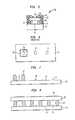
- FIG. 1shows a cross-sectional view of sheet of devices before singulation.
- FIG. 2shows a cross-sectional view of one of these singulated but unpackaged devices 5 .
- a microstructure 12rests on a wafer substrate 10 and is enclosed by glass frits 22 and a cap wafer 20 .
- the electrical connector 14connects to the microstructure 12 through the wafer substrate 10 .
- the singulated device 6is then connected to a lead frame 8 by the electrical connectors 4 . This is shown in FIG. 3 .
- This deviceis then packaged and results in the singulated MEMS package 6 as shown in FIG. 4 .
- the package 2surrounds the device 5 while the electrical leads 4 provide an electrical connection from the device 5 to the outside of the package 2 .
- the package 2serves to the protect the device 5 from external hazards.
- each device 5needs to be placed in the package 2 individually.
- the final singulated device package 6is considerably larger than the singulated device itself 5 .
- the present inventionis directed to a hermetically sealed wafer scale package for MEMS devices.
- a MBMS substrate wafer with microstructuresis hermetically sealed to a cap wafer with fabricated circuitry to form an assembly.
- the cap waferis preferably patterned before being attached to the device substrate to form the assembly.
- a wafer sawis then used to singulate the cap wafer and wire bond is attached to electrically connect the cap wafer to the MEMS wafer.
- Overmoldis then applied to the structure to protect the wire bond. Solder balls are then attached to the cap wafer and the wafer saw is used to singulate the assembly into packaged MEMS devices.
- FIG. 1is a cross-sectional view of a MEMS package assembly according to the prior art
- FIG. 2is a cross-sectional view of a single MEMS package according to the prior art
- FIG. 3is a plan view of a capped MEMS die connected to a lead frame prior to being molded into a package, according to the prior art
- FIG. 4is a cross-sectional view of a MEMS packaged device, fully contained with lead wires, according to the prior art
- FIG. 5is a cross-sectional view of a hermetically sealed MEMS device in a wafer scale package according to one embodiment of the invention.
- FIG. 6is a diagram of a plan view of a microstructure substrate
- FIG. 7shows a cross-sectional view of a MEMS wafer substrate, in a step of the invention
- FIG. 8shows a cross-sectional view of a further step of the invention.
- FIG. 9shows a cross-sectional view close-up of the cap wafer according to a further step of the invention.
- FIG. 10shows a cross-sectional view of an alternative embodiment of a further step of the invention.
- FIG. 11shows a cross-sectional view close up of the cap wafer according to one step of the invention.
- FIG. 12shows a cross-sectional view of a further step of the invention
- FIG. 13shows a cross-sectional view of a further step of the invention
- FIG. 14shows a cross-sectional view of a further step of the invention.
- FIG. 15shows a cross-sectional view of a further step of the invention.
- FIG. 16shows a cross-sectional view of a completed invention, a singulated hermetic wafer scale package with a MEMS device.
- circuitryis fabricated directly on the top surface of the cap wafer. This can be done either before or after bonding, although before is preferable. If the wafer is conductive, the circuitry needs to be insulated by oxide or a deposited dielectric. Finally, the circuitry needs to be electrically connectable to other elements. This metal connection layer is covered by a protective dielectric layer. This layer has gaps which are filled by solder balls. These balls serve as the electrical connectors to the final packaged device.
- a flex circuitis attached to the cap wafer rather than the circuitry being fabricated directly on the surface of the cap wafer.
- the flex circuitis attached to the cap wafer using an adhesive material.
- This flex circuitconsists of a first level dielectric, a metalization layer, and a second level dielectric.
- the first level dielectricserves to secure the flex circuit to the adhesive.
- the metalization layerprovides the electrical connection along the flex circuit.
- the second level dielectricserves to protect the metalization from outside interference and to contain the solder ball which will provide the package's electrical connection to external applications.
- a cap wafer attached to the device substrate prior to dicing and packagingprovides more robust devices by preventing particles from collecting over sensitive surfaces of the devices and scratching the surfaces.
- the structureBy fabricating circuitry directly onto the cap wafer, or alternatively, by attaching a flex circuit to the cap wafer, and then by connecting this cap layer to the MEMS layer, the structure allows external devices to connect directly to the cap layer without the need of a further package structure or step, thereby creating a much smaller, more manageable, and faster produced single packaged device than is available in the prior art.
- FIG. 5shows a cross-section of a hermetically sealed wafer scale MEMS package 60 .
- a microstructure 12that is being protected, rests atop a wafer substrate 10 and is attached thereto.
- the wafer substrateis connected to a cap layer 20 by frit glass 22 .
- the cap wafer 20 , frit glass 22 , and wafer substrate 10serve to protect and hermetically seal the microstructure 12 so that it may operate without hazards caused by foreign objects.
- An electrical signalallows the microstructure 12 to communicate with the external world.
- the electric signal from the microstructure 12is carried through the wafer substrate to the electrical connector 14 .
- the wire bond 40connects the microstructure electrical connection 14 to additional circuitry on the cap wafer 30 .
- An overmold 50protects the wire bond 40 and electrical connector 14 from external damage.
- the overmold 50is typically an epoxy, filled with silica to reduce thermal expansion. It is poured in between the frit glass posts 22 and then hardens to cover and hold in place the electrical connectors 14 .
- Electrical connectorsconnect the cap circuitry 30 to external devices. Solder balls 52 provide a means of electrically connecting the flex circuit to external circuitry. By connecting to the cap circuitry 30 , the electrical connectors are also connected to the microstructure 12 .
- the device of the inventionmay be manufactured by the inventive process described below.
- the process of creating a hermetically sealed wafer scale MEMS packagebegins with a wafer substrate containing the microstructures.
- the application of frit glassis the next step of manufacturing for a hermetically scaled wafer package for MEMS device.
- FIG. 6shows a plan view of a wafer substrate 10 containing microstructures 12 .
- FIG. 7shows a cross-sectional view of the same wafer substrate.
- the microstructures 12are fabricated onto the wafer substrate 10 .
- Electrical connections 14which provide connections to the microstructure, are also fabricated into the substrate.
- the flit glass 22is placed on the wafer substrate so that it surrounds the microstructure.
- the cap wafer 20then is pressed to the frit glass 22 to hermetically seal the microstructures, as shown in FIG. 8 .
- the entire assemblythen is cooled so that the frit 22 becomes solid glass and forms a seal surrounding the microstructure 12 .
- each of the microstructures 12is thus hermetically sealed within an individual cavity that is not completely filled during the sealing process, thereby allowing movement of the microstructure 12 within the cavity.
- the cap wafer 20prior to being sealed to the frit glass 22 , the cap wafer 20 is prefabricated with individual circuits 30 along its surface. These circuits 30 are lined up directly above the microstructure 12 when the cap wafer 20 is sealed to the substrate wafer 10 .
- FIG. 9shows a close-up of the cap wafer 20 according to the preferred embodiment of the invention.
- a dielectric 33is attached above the cap layer 20 in such a way that it protects the electrical connector 31 while creating an opening 25 which allows external devices to electrically connect to the circuitry on the cap wafer.
- the external devicesconnect at the dielectric gap 35 to the electrical connector 31 , which, in turn, connects to the circuitry 30 fabricated on the cap wafer 20 .
- FIG. 10shows a cross-sectional view of the substrate wafer 10 and the cap wafer 20 according to an alternative embodiment of the invention.
- a flex circuit 38 containing circuitry 32is attached to the cap wafer 20 .
- FIG. 11shows a close up of the cross-sectional view of the flex circuit 38 attached to the cap wafer 20 .
- the flex circuitconsists of a first level dielectric 34 , circuitry 32 , and a second level dielectric 36 .
- An adhesive layer 24connects the flex circuit 38 to the cap wafer 20 .
- the first level dielectricserves to protect the circuitry 32 from the adhesive bond layer 24 .
- the second level dielectric 36serves to protect the circuitry 32 from external hazards and is arranged in a way so that is creates a gap 35 in the second level dielectric 36 which allows access to the circuitry 32 . External devices connect to the circuitry 32 through this gap 35 in the second level dielectric 36 .
- This alternative embodimentmay be used in lieu of direct fabrication of circuitry onto the cap wafer.
- the next step in the process of the inventionis to separate the cap wafer so that the unnecessary portions of the cap wafer are removed and access can be gained to the underlying portions of the substrate wafer.
- FIG. 12shows this step of the invention.
- the cap wafer 20is separated by a wafer saw so that only the necessary portions of cap wafer remain.
- the next step of the invention processis shown in FIG. 13 . During this step, wire bond 40 is attached to the cap wafer circuit 30 and is connected to the electronic connection 14 of the microstructure 12 .
- the wire bondis typically applied by the use of a capillary which bonds the wire to the circuitry on the cap wafer, spools the wire to the electrical connectors 14 on the microstructure wafer and bonds the wire there. The capillary then severs the wire and moves to the next microstructure.
- the wire bondis made of gold but can be made of other similar materials such as aluminum.
- a ball of wire bond 42is formed by sealing the wire bond 40 to the connector 14 .
- an overmold 50preferably an epoxy in liquid form filled with silica to reduce thermal expansion, is poured between the microstructure glass seals 22 .
- the overmoldthen cools and then serves to protect the wire bond 40 which connects the cap wafer 20 to the substrate wafer 10 .
- the completion of this stepis shown in FIG. 14 .
- the next stepis to attached solder balls 52 to the cap wafer circuit 30 . This is shown in FIG. 15 . External applications connect through the solder balls 52 to the cap wafer and through it connect to the microstructure 12 .
- the final stepis to singulate the hermetically sealed wafer scale packaged MEMS.
- a wafer sawis used to cut through the overmold 50 and create the singulated packages 60 .
- the result of this stepis shown in FIG. 16 .
- the final packagesare wafer scale, or “chip-sized.” This means that the final packages are the same size as the singulated devices. There is no external casing required which changes the size of the final package.
- the manufacturing processcould be halted and testing could be performed on the individual microstructure packages or on the entire wafer. This ability to test at the wafer level contributes to the low cost of these microstructure devices.
Landscapes
- Engineering & Computer Science (AREA)
- Microelectronics & Electronic Packaging (AREA)
- Computer Hardware Design (AREA)
- Manufacturing & Machinery (AREA)
- Physics & Mathematics (AREA)
- Condensed Matter Physics & Semiconductors (AREA)
- General Physics & Mathematics (AREA)
- Power Engineering (AREA)
- Micromachines (AREA)
Abstract
Description
This application is a divisional of U.S. application Ser. No. 09/546,864, filed on Apr. 10, 2000, entitled “Hermetically Sealed Microstructure Package” and now U.S. Pat. No. 6,441,481.
The present invention relates to semiconductor devices, and more particularly, to a protective cover arrangement for a semiconductor substrate containing micro-mechanical devices, wherein the cover arrangement offers more desirable protection and manufacturing characteristics.
A variety of semiconductor devices may be formed on a substrate according to several known techniques. The semiconductor devices may perform, for examples, electrical, mechanical, optical, or other functions, or combinations of such functions.
Often, a semiconductor wafer serves as a substrate for such devices. The devices may be fabricated from the semiconductor material of the substrate wafer itself using a variety of known processes, such as growth of various material layers on a surface of the substrate, ion implantation, diffusion, oxidation, photolithography, etching and many other processes. During fabrication, typically, at least some portion of each device is formed “within” the substrate wafer, below the surface of the substrate, and may additionally include particular topographic or structural features on the substrate surface.
Alternatively, semiconductor devices may be fabricated from a first semiconductor wafer, and subsequently mounted on a second semiconductor wafer or other type of material that serves as a substrate. The semiconductor devices fabricated from the first wafer may be mounted on the substrate either as individual devices or groups of devices. In this case, the devices “reside on” the substrate, as opposed to being “fabricated from” the substrate, as discussed above.
For purposes of the present invention, either of the foregoing examples of substrates, namely, substrates on which semiconductor devices reside, and/or from which semiconductor devices are fabricated, is referred to as a “device” substrate. A device substrate may include one or a large number of devices.
Many known semiconductor devices are extremely fragile and/or sensitive to environmental hazards. Some examples of such hazards include contamination by dust or other particles, moisture, and inadvertent scratching or other damage to portions of the surface of the devices.
Functional defects may result from one or more environmental hazards, as discussed above, and are a major cause of low device yield and other malperformance characteristics. Device damage due to any number of such hazards may occur, for example, during the process of “dicing” (separating the device substrate into individual devices), as well as during packaging of devices. Often, the number of functioning devices remaining after dicing and packaging is markedly reduced due to defects resulting from environmental hazards.
Various techniques are known in the art for protecting semiconductor devices on a substrate from such hazards. One of these techniques includes bonding a protective semiconductor cap wafer to a device substrate before dicing the substrate into individual devices. This technique has been employed particularly with wafer substrates of semiconductor devices that include micro-machined parts or microscopic mechanisms fabricated on the surface of the substrate, such as micro-electrical-mechanical systems, or MEMS. These devices are also referred to as microstructures.
According to one known technique for protecting semiconductor micro-mechanical devices, an entire device substrate wafer is capped with another wafer using a pattern of glass-like posts called “frit glass” as a bonding agent. In this technique, the micro-mechanical devices are hermetically sealed inside an open cavity formed by the frit glass pattern, the device substrate and the cap wafer. Hermetic sealing refers to a particular standard for sealing that is known in the art. Accordingly, any micro-mechanisms are free to move within a cavity while simultaneously being protected from various environmental hazards, such as particulate contamination.
According to the technique discussed above, the cap wafer is typically another semiconductor wafer of the same type as that used for the device substrate (for example, silicon or gallium arsenide). As a result, the cap wafer has essentially identical thermal characteristics to that of the device substrate. Such a choice of cap wafer results in avoiding most mechanical stresses that may result from a thermal mismatch between the cap wafer and the device substrate. For example, extreme mechanical stress can occur during a high temperature heat treatment necessary to ensure adequate bonding of the frit glass to the cap wafer and the device substrate. Any mechanical stress can severely damage or even destroy the devices on the substrate, and usually would degrade the accuracy of many delicate micro-machined devices, such as microscopic mechanical sensors or other MEMS.
After the micro-mechanism has been protected by wafer capping, the individual devices must be prepared for connection to external circuits. This process consists of separating the individual devices through dividing the substrate into individual devices, called “singulating” or “dicing.” After singulation, the devices are placed into individual containers that provide mechanical protection and electrical connections to the microstructures. This process is called “packaging.” This process of fabricating micro-mechanism packages is time consuming, expensive and results in large devices, as a consequence of processing the individual devices as individual devices.
FIG. 1 shows a cross-sectional view of sheet of devices before singulation. FIG. 2 shows a cross-sectional view of one of these singulated butunpackaged devices 5. Amicrostructure 12 rests on awafer substrate 10 and is enclosed byglass frits 22 and acap wafer 20. Theelectrical connector 14 connects to themicrostructure 12 through thewafer substrate 10. The singulateddevice 6 is then connected to alead frame 8 by theelectrical connectors 4. This is shown in FIG.3. This device is then packaged and results in the singulatedMEMS package 6 as shown in FIG.4. Thepackage 2 surrounds thedevice 5 while theelectrical leads 4 provide an electrical connection from thedevice 5 to the outside of thepackage 2. Thepackage 2 serves to the protect thedevice 5 from external hazards.
In order to create the individual packageddevice 6, eachdevice 5 needs to be placed in thepackage 2 individually. The final singulateddevice package 6 is considerably larger than the singulated device itself5.
Accordingly, what is needed, therefore, is improved packaging which still provides the necessary protection, space and connectibility to the microstructure contained inside.
Accordingly, the present invention is directed to a hermetically sealed wafer scale package for MEMS devices. According to the method and apparatus of one embodiment of the invention, a MBMS substrate wafer with microstructures is hermetically sealed to a cap wafer with fabricated circuitry to form an assembly. The cap wafer is preferably patterned before being attached to the device substrate to form the assembly. A wafer saw is then used to singulate the cap wafer and wire bond is attached to electrically connect the cap wafer to the MEMS wafer. Overmold is then applied to the structure to protect the wire bond. Solder balls are then attached to the cap wafer and the wafer saw is used to singulate the assembly into packaged MEMS devices.
The accompanying drawings are not intended to be drawn to scale. In the drawings, each identical or nearly identical component that is illustrated in various figures is represented by a like numeral. For purposes of clarity, not every component may be labeled in every drawing.
FIG. 1 is a cross-sectional view of a MEMS package assembly according to the prior art;
FIG. 2 is a cross-sectional view of a single MEMS package according to the prior art;
FIG. 3 is a plan view of a capped MEMS die connected to a lead frame prior to being molded into a package, according to the prior art;
FIG. 4 is a cross-sectional view of a MEMS packaged device, fully contained with lead wires, according to the prior art;
FIG. 5 is a cross-sectional view of a hermetically sealed MEMS device in a wafer scale package according to one embodiment of the invention;
FIG. 6 is a diagram of a plan view of a microstructure substrate;
FIG. 7 shows a cross-sectional view of a MEMS wafer substrate, in a step of the invention;
FIG. 8 shows a cross-sectional view of a further step of the invention;
FIG. 9 shows a cross-sectional view close-up of the cap wafer according to a further step of the invention;
FIG. 10 shows a cross-sectional view of an alternative embodiment of a further step of the invention;
FIG. 11 shows a cross-sectional view close up of the cap wafer according to one step of the invention;
FIG. 12 shows a cross-sectional view of a further step of the invention;
FIG. 13 shows a cross-sectional view of a further step of the invention;
FIG. 14 shows a cross-sectional view of a further step of the invention;
FIG. 15 shows a cross-sectional view of a further step of the invention;
FIG. 16 shows a cross-sectional view of a completed invention, a singulated hermetic wafer scale package with a MEMS device.
In view of the foregoing, it would be advantageous to protect semiconductors such as MEMS devices, on a “wafer” level; namely, simultaneously protecting one or more devices residing on or fabricated from a device substrate, as opposed to protecting individual devices after the device wafer has been diced. Furthermore, it would be advantageous to manufacture these devices in such a way that they will be easily connected to their external applications using a minimum of space and a minimum of manufacturing processes.
In the preferred embodiment of the invention, circuitry is fabricated directly on the top surface of the cap wafer. This can be done either before or after bonding, although before is preferable. If the wafer is conductive, the circuitry needs to be insulated by oxide or a deposited dielectric. Finally, the circuitry needs to be electrically connectable to other elements. This metal connection layer is covered by a protective dielectric layer. This layer has gaps which are filled by solder balls. These balls serve as the electrical connectors to the final packaged device.
In an alternative embodiment, a flex circuit is attached to the cap wafer rather than the circuitry being fabricated directly on the surface of the cap wafer. In this embodiment the flex circuit is attached to the cap wafer using an adhesive material. This flex circuit consists of a first level dielectric, a metalization layer, and a second level dielectric. The first level dielectric serves to secure the flex circuit to the adhesive. The metalization layer provides the electrical connection along the flex circuit. The second level dielectric serves to protect the metalization from outside interference and to contain the solder ball which will provide the package's electrical connection to external applications.
A cap wafer attached to the device substrate prior to dicing and packaging provides more robust devices by preventing particles from collecting over sensitive surfaces of the devices and scratching the surfaces.
By fabricating circuitry directly onto the cap wafer, or alternatively, by attaching a flex circuit to the cap wafer, and then by connecting this cap layer to the MEMS layer, the structure allows external devices to connect directly to the cap layer without the need of a further package structure or step, thereby creating a much smaller, more manageable, and faster produced single packaged device than is available in the prior art.
FIG. 5 shows a cross-section of a hermetically sealed waferscale MEMS package 60. Amicrostructure 12, that is being protected, rests atop awafer substrate 10 and is attached thereto. The wafer substrate is connected to acap layer 20 byfrit glass 22. Thecap wafer 20,frit glass 22, andwafer substrate 10, serve to protect and hermetically seal themicrostructure 12 so that it may operate without hazards caused by foreign objects. An electrical signal allows themicrostructure 12 to communicate with the external world. The electric signal from themicrostructure 12 is carried through the wafer substrate to theelectrical connector 14. Thewire bond 40 connects the microstructureelectrical connection 14 to additional circuitry on thecap wafer 30. Anovermold 50 protects thewire bond 40 andelectrical connector 14 from external damage. Theovermold 50 is typically an epoxy, filled with silica to reduce thermal expansion. It is poured in between the frit glass posts22 and then hardens to cover and hold in place theelectrical connectors 14. Electrical connectors connect thecap circuitry 30 to external devices.Solder balls 52 provide a means of electrically connecting the flex circuit to external circuitry. By connecting to thecap circuitry 30, the electrical connectors are also connected to themicrostructure 12. The device of the invention may be manufactured by the inventive process described below.
The process of creating a hermetically sealed wafer scale MEMS package begins with a wafer substrate containing the microstructures. The application of frit glass is the next step of manufacturing for a hermetically scaled wafer package for MEMS device.
FIG. 6 shows a plan view of awafer substrate 10 containingmicrostructures 12.
The left-most microstructure is surrounded by a ring offrit glass 22. FIG. 7 shows a cross-sectional view of the same wafer substrate. Themicrostructures 12 are fabricated onto thewafer substrate 10.Electrical connections 14, which provide connections to the microstructure, are also fabricated into the substrate.
At the next step of the process, theflit glass 22 is placed on the wafer substrate so that it surrounds the microstructure. Thecap wafer 20 then is pressed to thefrit glass 22 to hermetically seal the microstructures, as shown in FIG.8. The entire assembly then is cooled so that the frit22 becomes solid glass and forms a seal surrounding themicrostructure 12. As shown in FIG. 8, each of themicrostructures 12 is thus hermetically sealed within an individual cavity that is not completely filled during the sealing process, thereby allowing movement of themicrostructure 12 within the cavity.
According to the preferred embodiment of the invention, prior to being sealed to thefrit glass 22, thecap wafer 20 is prefabricated withindividual circuits 30 along its surface. Thesecircuits 30 are lined up directly above themicrostructure 12 when thecap wafer 20 is sealed to thesubstrate wafer 10.
FIG. 9 shows a close-up of thecap wafer 20 according to the preferred embodiment of the invention. A dielectric33 is attached above thecap layer 20 in such a way that it protects theelectrical connector 31 while creating an opening25 which allows external devices to electrically connect to the circuitry on the cap wafer. The external devices connect at thedielectric gap 35 to theelectrical connector 31, which, in turn, connects to thecircuitry 30 fabricated on thecap wafer 20.
FIG. 10 shows a cross-sectional view of thesubstrate wafer 10 and thecap wafer 20 according to an alternative embodiment of the invention. According to this embodiment, aflex circuit 38 containingcircuitry 32 is attached to thecap wafer 20. FIG. 11 shows a close up of the cross-sectional view of theflex circuit 38 attached to thecap wafer 20. The flex circuit consists of afirst level dielectric 34,circuitry 32, and asecond level dielectric 36. Anadhesive layer 24 connects theflex circuit 38 to thecap wafer 20. The first level dielectric serves to protect thecircuitry 32 from theadhesive bond layer 24. Thesecond level dielectric 36 serves to protect thecircuitry 32 from external hazards and is arranged in a way so that is creates agap 35 in thesecond level dielectric 36 which allows access to thecircuitry 32. External devices connect to thecircuitry 32 through thisgap 35 in thesecond level dielectric 36. This alternative embodiment may be used in lieu of direct fabrication of circuitry onto the cap wafer.
After thecap wafer 20 is sealed to thesubstrate wafer 10, the next step in the process of the invention is to separate the cap wafer so that the unnecessary portions of the cap wafer are removed and access can be gained to the underlying portions of the substrate wafer. FIG. 12 shows this step of the invention. In the preferred embodiment of the invention, thecap wafer 20 is separated by a wafer saw so that only the necessary portions of cap wafer remain. The next step of the invention process is shown in FIG.13. During this step,wire bond 40 is attached to thecap wafer circuit 30 and is connected to theelectronic connection 14 of themicrostructure 12. The wire bond is typically applied by the use of a capillary which bonds the wire to the circuitry on the cap wafer, spools the wire to theelectrical connectors 14 on the microstructure wafer and bonds the wire there. The capillary then severs the wire and moves to the next microstructure. In the preferred embodiment, the wire bond is made of gold but can be made of other similar materials such as aluminum. At the base of the connection of thewire bond 40 to theMEMS connector 14, a ball ofwire bond 42 is formed by sealing thewire bond 40 to theconnector 14.
During the next step of the process, anovermold 50, preferably an epoxy in liquid form filled with silica to reduce thermal expansion, is poured between the microstructure glass seals22. The overmold then cools and then serves to protect thewire bond 40 which connects thecap wafer 20 to thesubstrate wafer 10. The completion of this step is shown in FIG.14.
The next step is to attachedsolder balls 52 to thecap wafer circuit 30. This is shown in FIG.15. External applications connect through thesolder balls 52 to the cap wafer and through it connect to themicrostructure 12.
The final step is to singulate the hermetically sealed wafer scale packaged MEMS. In the preferred embodiment, a wafer saw is used to cut through theovermold 50 and create the singulated packages60. The result of this step is shown in FIG.16. The final packages are wafer scale, or “chip-sized.” This means that the final packages are the same size as the singulated devices. There is no external casing required which changes the size of the final package.
In between any of the steps above, the manufacturing process could be halted and testing could be performed on the individual microstructure packages or on the entire wafer. This ability to test at the wafer level contributes to the low cost of these microstructure devices.
Having thus described at least one illustrated embodiment of the invention, various alterations, modifications, and improvements will readily occur to those skilled in the art.
Such alterations, modifications, and improvements are intended to be in the spirit of the invention. Accordingly, the foregoing description is by way of example only and is not intended as limiting.
Claims (49)
1. A process for manufacturing microstructure packages, comprising steps of:
hermetically sealing a plurality of microstructures on a substrate, each microstructure being hermetically sealed within an individual cavity that is not completely filled during the sealing process, thereby allowing movement of the microstructure within the cavity;
providing electrical connections to the individual microstructures;
disposing a protective dielectric substance over the electrical connections while the substrate is intact; and
dividing the substrate having the microstructures sealed thereon into sections so as to form individual microstructure assemblies.
2. The process ofclaim 1 , wherein the step of providing electrical connections comprises electrically connecting each microstructure to circuitry on or in an upper portion of the seal for that microstructure.
3. The process ofclaim 2 , wherein the step of electrically connecting comprises:
electrically connecting each microstructure to corresponding circuitry on or in the substrate; and
electrically connecting the corresponding circuitry on or in the substrate for each microstructure to the circuitry on or in the upper portion of the seal for that microstructure.
4. The process ofclaim 3 , wherein the step of electrically connecting further comprises using wire bonds to electrically connect the circuitry on or in the substrate for each microstructure to the circuitry on or in the upper portion of the seal for that microstructure.
5. The process ofclaim 4 , wherein the step of disposing the protective dielectric substance over the electrical connections comprises disposing an overmold over the wire bonds.
6. The process ofclaim 1 , wherein the step of hermetically sealing comprises:
surrounding each microstructure with a coolable material;
attaching a cap to the coolable material surrounding each microstructure; and
allowing the coolable material to cool thereby forming hermetically sealed cavities containing the microstructures.
7. The process ofclaim 6 , wherein the coolable material comprises flit glass.
8. The process ofclaim 6 , wherein the cap comprises a wafer that has circuitry fabricated thereon at the time the step of attaching the cap to the coolable material is performed.
9. The process ofclaim 6 , wherein the cap comprises a wafer with an attached flex circuit.
10. The process ofclaim 1 , wherein the step of dividing comprises using a wafer saw to separate-the microstructure assemblies.
11. The process ofclaim 1 , wherein the step of providing electrical connections comprises using wire bonds to electrically connect circuitry on or in the substrate to circuitry on or in upper portions of the seals of the microstructures.
12. The process ofclaim 1 , wherein the step of disposing the protective dielectric substance over the electrical connections comprises disposing an overmold between the microstructure cavities.
13. The process ofclaim 1 , wherein the step of providing electrical connections is performed after the step of hermetically sealing the plurality of microstructures has been performed.
14. The process ofclaim 1 , wherein the plurality of microstructures comprises MEMS devices.
15. The process ofclaim 1 , wherein the step of disposing the protective dielectric substance over the electrical connections comprises disposing an overmold over the electrical connections.
16. The process ofclaim 1 , wherein:
the step of hermetically sealing comprises using a single wafer cap to simultaneously hermetically seal the plurality of microstructures on the substrate; and
the process further comprises a step of removing portions of the single wafer cap while the substrate is intact to provide access to areas thereunder.
17. The process ofclaim 16 , wherein the step of hermetically sealing further comprises attaching the wafer cap to glass surrounding the plurality of microstructures.
18. The process ofclaim 1 , wherein:
the step of hermetically sealing comprises attaching a wafer cap to glass surrounding each microstructure.
19. A process for manufacturing wafer-scale microstructure packages, comprising steps of:
hermetically sealing a plurality of microstructures on a substrate while the substrate is intact, each microstructure being hermetically sealed within a cavity that is not completely filled during the sealing process, thereby allowing movement of the microstructure within the cavity;
separating the substrate having the microstructures sealed thereon into sections so as to form individual microstructure packages; and
before separating the substrate to form the individual microstructure packages, securing electrically conductive leads to each of the packages, the leads being configured and arranged to directly contact circuitry on a circuit board and to electrically connect the microstructure in the package to that circuitry.
20. The process ofclaim 19 , wherein the step of hermetically sealing comprises sealing the microstructures within the cavities so that the microstructures are free to move within the cavities.
21. The process ofclaim 19 , wherein the plurality of microstructures comprises MEMS devices.
22. The process ofclaim 19 , wherein:
the step of hermetically sealing comprises using a single wafer cap to simultaneously hermetically seal the plurality of microstructures on the substrate; and
the process further comprises a step of removing portions of the single wafer cap while the substrate is intact to provide access to areas thereunder.
23. The process ofclaim 22 , wherein the step of hermetically sealing further comprises attaching the wafer cap to glass surrounding the plurality of microstructures.
24. The process ofclaim 19 , wherein:
the step of hermetically sealing comprises attaching a wafer cap to glass surrounding each microstructure.
25. A microstructure package manufactured according to a process, the process comprising steps of:
hermetically sealing a plurality of microstructures on a substrate, each microstructure being hermetically sealed within an individual cavity that is not completely filled during the sealing step, thereby allowing the microstructure to move within the cavity;
providing electrical connections to the individual microstructures;
disposing a protective dielectric substance over the electrical connections while the substrate is intact; and
dividing the substrate having the microstructures sealed thereon into sections so as to form individual microstructure assemblies.
26. The microstructure package manufactured according to the process ofclaim 25 , wherein the process step of providing electrical connections comprises electrically connecting each microstructure to circuitry on or in an upper portion of the seal for that microstructure.
27. The microstructure package manufactured according to the process ofclaim 26 , wherein the step of electrically connecting comprises:
electrically connecting each microstructure to corresponding circuitry on or in the substrate; and
electrically connecting the corresponding circuitry on or in the substrate for each microstructure to the circuitry on or in the upper portion of the seal for that microstructure.
28. The microstructure package manufactured according to the process ofclaim 27 , wherein the step of electrically connecting further comprises using wire bonds to electrically connect the circuitry on or in the substrate for each microstructure to the circuitry on or in the upper portion of the seal for that microstructure.
29. The microstructure package manufactured according to the process ofclaim 28 , wherein the step of disposing the protective dielectric substance over the electrical connections comprises disposing an overmold over the wire bonds.
30. The microstructure package manufactured according to the process ofclaim 25 , wherein the process step of hermetically sealing comprises:
surrounding each microstructure with a coolable material;
attaching a cap to the coolable material surrounding each microstructure; and
allowing the coolable material to cool thereby forming hermetically sealed cavities containing the microstructures.
31. The microstructure package manufactured according to the process ofclaim 30 , wherein the cap comprises a wafer that has circuitry fabricated thereon at the time the step of attaching the cap to the coolable material is performed.
32. The microstructure package manufactured according to the process ofclaim 30 , wherein the cap comprises a wafer with an attached flex circuit.
33. The microstructure package manufactured according to the process of claim wherein the coolable material comprises frit glass.
34. The microstructure package manufactured according to the process ofclaim 25 , wherein the process step of dividing comprises using a wafer saw to separate the microstructure assemblies.
35. The microstructure package manufactured according to the process ofclaim 25 , wherein the process step of providing electrical connections comprises using wire bonds to electrically connect circuitry on or in the substrate to circuitry on or in upper portions of the seals of the microstructures.
36. The microstructure package manufactured according to the process ofclaim 25 , wherein the process step of disposing the protective dielectric substance over the electrical connections comprises disposing an overmold between the microstructure cavities.
37. The microstructure package manufactured according to the process ofclaim 25 , wherein the step providing electrical connections is performed after the step of hermetically sealing the plurality of microstructures.
38. The microstructure package manufactured according to the process ofclaim 25 , wherein the plurality of microstructures comprises MEMS devices.
39. The microstructure package manufactured according to the process ofclaim 25 , wherein the step of disposing the protective dielectric substance over the electrical connections comprises disposing an overmold over the electrical connections.
40. The microstructure package manufactured according to the process ofclaim 25 , wherein:
the process step of hermetically sealing comprises using a single wafer cap to simultaneously hermetically seal the plurality of microstructures on the substrate; and
the process further comprises a step of removing portions of the single wafer cap while the substrate is intact to provide access to areas thereunder.
41. The microstructure package manufactured according to the process ofclaim 40 , wherein the process step of hermetically sealing further comprises attaching the wafer cap to glass surrounding the plurality of microstructures.
42. The microstructure package manufactured according to the process of claim therein the process step of hermetically sealing comprises attaching a wafer cap to glass surrounding each microstructure.
43. A microstructure package manufactured according to a process, the process comprising the following steps:
hermetically sealing a plurality of microstructures on a substrate while the substrate is intact, each microstructure being hermetically sealed within a cavity that is not completely filled during the sealing process, thereby allowing the microstructure to move within the cavity;
separating the substrate having the microstructures sealed thereon into sections so as to form individual microstructure packages; and
before separating the substrate to form the individual microstructure packages, securing electrically conductive leads to each of the packages, the leads being configured and arranged to directly contact circuitry on a circuit board and to electrically connect the microstructure in the package to that circuitry.
44. The microstructure package manufactured according to the process ofclaim 43 , wherein the plurality of microstructures comprises MEMS devices.
45. The microstructure package manufactured according to the process ofclaim 43 , wherein:
the process step of hermetically sealing comprises using a single wafer cap to simultaneously hermetically seal the plurality of microstructures on the substrate; and
the process further comprises a step of removing portions of the single wafer cap while the substrate is intact to provide access to areas thereunder.
46. The micro structure package manufactured according to the process ofclaim 45 , wherein the process step of hermetically sealing further comprises attaching the wafer cap to glass surrounding the plurality of microstructures.
47. The microstructure package manufactured according to the process ofclaim 43 , wherein the step of hermetically sealing comprises attaching a wafer cap to glass surrounding each microstructure.
48. A process for manufacturing MEMS device packages, comprising steps of:
hermetically sealing a plurality of MEMS devices on a substrate, each MEMS device being hermetically sealed within an individual cavity;
providing electrical connections to the individual MEMS devices;
disposing a protective dielectric substance over the electrical connections while the substrate is intact; and
dividing the substrate having the MEMS devices hermetically sealed thereon into sections so as to form individual MEMS device assemblies.
49. A process for manufacturing MEMS device packages, comprising steps of:
hermetically sealing a plurality of MEMS devices on a substrate while the substrate is intact;
separating the substrate having the MEMS devices hermetically sealed thereon into sections so as to form individual MEMS device packages; and
before separating the substrate to form the individual microstructure packages, securing electrically conductive leads to each of the packages, the leads being configured and arranged to directly contact circuitry on a circuit board and to electrically connect the microstructure in the package to that circuitry.
Priority Applications (1)
| Application Number | Priority Date | Filing Date | Title |
|---|---|---|---|
| US10/164,064US6828674B2 (en) | 2000-04-10 | 2002-06-05 | Hermetically sealed microstructure package |
Applications Claiming Priority (2)
| Application Number | Priority Date | Filing Date | Title |
|---|---|---|---|
| US09/546,864US6441481B1 (en) | 2000-04-10 | 2000-04-10 | Hermetically sealed microstructure package |
| US10/164,064US6828674B2 (en) | 2000-04-10 | 2002-06-05 | Hermetically sealed microstructure package |
Related Parent Applications (1)
| Application Number | Title | Priority Date | Filing Date |
|---|---|---|---|
| US09/546,864DivisionUS6441481B1 (en) | 2000-04-10 | 2000-04-10 | Hermetically sealed microstructure package |
Publications (2)
| Publication Number | Publication Date |
|---|---|
| US20030006502A1 US20030006502A1 (en) | 2003-01-09 |
| US6828674B2true US6828674B2 (en) | 2004-12-07 |
Family
ID=24182349
Family Applications (2)
| Application Number | Title | Priority Date | Filing Date |
|---|---|---|---|
| US09/546,864Expired - LifetimeUS6441481B1 (en) | 2000-04-10 | 2000-04-10 | Hermetically sealed microstructure package |
| US10/164,064Expired - LifetimeUS6828674B2 (en) | 2000-04-10 | 2002-06-05 | Hermetically sealed microstructure package |
Family Applications Before (1)
| Application Number | Title | Priority Date | Filing Date |
|---|---|---|---|
| US09/546,864Expired - LifetimeUS6441481B1 (en) | 2000-04-10 | 2000-04-10 | Hermetically sealed microstructure package |
Country Status (1)
| Country | Link |
|---|---|
| US (2) | US6441481B1 (en) |
Cited By (55)
| Publication number | Priority date | Publication date | Assignee | Title |
|---|---|---|---|---|
| US20030159278A1 (en)* | 2002-02-26 | 2003-08-28 | Peddle Charles I. | Methods and apparatus for fabricating Chip-on-Board modules |
| US20040121517A1 (en)* | 2001-01-10 | 2004-06-24 | Silverbrook Research Pty Ltd | Placement tool for wafer scale caps |
| US20040212059A1 (en)* | 2003-02-28 | 2004-10-28 | Takuji Kato | Circuit device and method for manufacturing the same |
| US20050110889A1 (en)* | 2003-11-26 | 2005-05-26 | Tuttle Mark E. | Packaged microelectronic imagers and methods of packaging microelectronic imagers |
| US6934065B2 (en)* | 2003-09-18 | 2005-08-23 | Micron Technology, Inc. | Microelectronic devices and methods for packaging microelectronic devices |
| US20050184219A1 (en)* | 2004-02-23 | 2005-08-25 | Kirby Kyle K. | Packaged microelectronic imagers and methods of packaging microelectronic imagers |
| US20050254133A1 (en)* | 2004-05-13 | 2005-11-17 | Salman Akram | Integrated optics units and methods of manufacturing integrated optics units for use with microelectronic imagers |
| US20050275051A1 (en)* | 2004-06-14 | 2005-12-15 | Farnworth Warren M | Prefabricated housings for microelectronic imagers and methods for packaging microelectronic imagers |
| US20050275049A1 (en)* | 2004-06-10 | 2005-12-15 | Kirby Kyle K | Packaged microelectronic imagers and methods of packging microelectronic imagers |
| US20050275750A1 (en)* | 2004-06-09 | 2005-12-15 | Salman Akram | Wafer-level packaged microelectronic imagers and processes for wafer-level packaging |
| US20050275048A1 (en)* | 2004-06-14 | 2005-12-15 | Farnworth Warren M | Microelectronic imagers and methods of packaging microelectronic imagers |
| US20050285154A1 (en)* | 2004-06-29 | 2005-12-29 | Salman Akram | Packaged microelectronic imagers and methods of packaging microelectronic imagers |
| US20060014313A1 (en)* | 2004-07-16 | 2006-01-19 | Hall Frank L | Microelectronic imaging units and methods of manufacturing microelectronic imaging units |
| US20060011809A1 (en)* | 2004-07-19 | 2006-01-19 | Farnworth Warren M | Microelectronic imagers with optical devices and methods of manufacturing such microelectronic imagers |
| US20060024856A1 (en)* | 2004-07-28 | 2006-02-02 | Derderian James M | Microelectronic imaging units and methods of manufacturing microelectronic imaging units |
| US20060038183A1 (en)* | 2004-08-19 | 2006-02-23 | Oliver Steven D | Microelectronic imagers with curved image sensors and methods for manufacturing microelectronic imagers |
| US20060040421A1 (en)* | 2004-08-19 | 2006-02-23 | Farnworth Warren M | Spacers for packaged microelectronic imagers and methods of making and using spacers for wafer-level packaging of imagers |
| US20060043599A1 (en)* | 2004-09-02 | 2006-03-02 | Salman Akram | Through-wafer interconnects for photoimager and memory wafers |
| US20060043509A1 (en)* | 2004-08-24 | 2006-03-02 | Watkins Charles M | Packaged microelectronic imaging devices and methods of packaging microelectronic imaging devices |
| US20060043512A1 (en)* | 2004-08-24 | 2006-03-02 | Oliver Steven D | Microelectronic imagers with optical devices having integral reference features and methods for manufacturing such microelectronic imagers |
| US20060044433A1 (en)* | 2004-08-31 | 2006-03-02 | Micron Technology, Inc. | Microelectronic imagers having front side contacts and methods of packaging such microelectronic imagers |
| US20060046332A1 (en)* | 2004-08-26 | 2006-03-02 | Derderian James M | Microelectronic Imaging units and methods of manufacturing microelectronic imaging units |
| US20060043262A1 (en)* | 2004-08-30 | 2006-03-02 | Micron Technology, Inc. | Microelectronic imagers with integrated optical devices and methods for manufacturing such microelectronic imagers |
| US20060076670A1 (en)* | 2004-10-08 | 2006-04-13 | Lim Ohk K | Micro-electro-mechanical system (MEMS) package having metal sealing member |
| US20060148250A1 (en)* | 2004-12-30 | 2006-07-06 | Micron Technology, Inc. | Methods for forming interconnects in microelectronic workpieces and microelectronic workpieces formed using such methods |
| US20060160273A1 (en)* | 2005-01-19 | 2006-07-20 | Chih-Hsien Chen | Method for wafer level packaging |
| US20060175532A1 (en)* | 2005-02-08 | 2006-08-10 | Micron Technology, Inc. | Microelectronic imaging units and methods of manufacturing microelectronic imaging units |
| US20060177959A1 (en)* | 2005-02-10 | 2006-08-10 | Micron Technology, Inc. | Microfeature workpieces having microlenses and methods of forming microlenses on microfeature workpieces |
| US20060186492A1 (en)* | 2005-02-18 | 2006-08-24 | Micron Technology, Inc. | Microelectronic imagers with shaped image sensors and methods for manufacturing microelectronic imagers |
| US20060211233A1 (en)* | 2005-03-21 | 2006-09-21 | Skyworks Solutions, Inc. | Method for fabricating a wafer level package having through wafer vias for external package connectivity and related structure |
| US20060289968A1 (en)* | 2005-06-28 | 2006-12-28 | Micron Technology, Inc. | Conductive interconnect structures and formation methods using supercritical fluids |
| US20070045515A1 (en)* | 2005-09-01 | 2007-03-01 | Micron Technology, Inc. | Microelectronic imaging devices and associated methods for attaching transmissive elements |
| US7232754B2 (en) | 2004-06-29 | 2007-06-19 | Micron Technology, Inc. | Microelectronic devices and methods for forming interconnects in microelectronic devices |
| US20070148807A1 (en)* | 2005-08-22 | 2007-06-28 | Salman Akram | Microelectronic imagers with integrated optical devices and methods for manufacturing such microelectronic imagers |
| US20070176280A1 (en)* | 2006-02-02 | 2007-08-02 | Stats Chippac Ltd. | Waferscale package system |
| US20070178666A1 (en)* | 2006-01-31 | 2007-08-02 | Stats Chippac Ltd. | Integrated circuit system with waferscale spacer system |
| US7262134B2 (en) | 2005-09-01 | 2007-08-28 | Micron Technology, Inc. | Microfeature workpieces and methods for forming interconnects in microfeature workpieces |
| US20070205087A1 (en)* | 2004-04-12 | 2007-09-06 | Pashby Gary J | Single-Pole Double-Throw Mems Switch |
| US7364934B2 (en) | 2004-08-10 | 2008-04-29 | Micron Technology, Inc. | Microelectronic imaging units and methods of manufacturing microelectronic imaging units |
| US7425499B2 (en) | 2004-08-24 | 2008-09-16 | Micron Technology, Inc. | Methods for forming interconnects in vias and microelectronic workpieces including such interconnects |
| US20090000968A1 (en)* | 2007-06-28 | 2009-01-01 | Philip Morris Usa Inc. | Innovative packaging for consumer product |
| US20090212407A1 (en)* | 2005-05-12 | 2009-08-27 | Foster Ron B | Infinitely Stackable Interconnect Device and Method |
| US7622377B2 (en) | 2005-09-01 | 2009-11-24 | Micron Technology, Inc. | Microfeature workpiece substrates having through-substrate vias, and associated methods of formation |
| USD614023S1 (en) | 2008-12-29 | 2010-04-20 | Philip Morris Usa Inc. | Package |
| US20100194465A1 (en)* | 2009-02-02 | 2010-08-05 | Ali Salih | Temperature compensated current source and method therefor |
| US20100244161A1 (en)* | 2007-11-30 | 2010-09-30 | Skyworks Solutions, Inc. | Wafer level packaging using flip chip mounting |
| US20100283144A1 (en)* | 2007-12-26 | 2010-11-11 | Steve Xin Liang | In-situ cavity circuit package |
| US20110177643A1 (en)* | 2010-01-20 | 2011-07-21 | Siliconware Precision Industries Co., Ltd. | Fabrication method of package structure having mems element |
| US20120001274A1 (en)* | 2010-06-30 | 2012-01-05 | Siliconware Precision Industries Co., Ltd. | Wafer level package having a pressure sensor and fabrication method thereof |
| US8092734B2 (en) | 2004-05-13 | 2012-01-10 | Aptina Imaging Corporation | Covers for microelectronic imagers and methods for wafer-level packaging of microelectronics imagers |
| CN102336390A (en)* | 2010-07-26 | 2012-02-01 | 矽品精密工业股份有限公司 | Micro-electromechanical structure with pressure sensor and manufacturing method thereof |
| USD655154S1 (en) | 2009-03-30 | 2012-03-06 | Philip Morris Usa Inc. | Package |
| US8154115B1 (en) | 2010-12-17 | 2012-04-10 | Siliconware Precision Industries Co., Ltd. | Package structure having MEMS element and fabrication method thereof |
| US20120266686A1 (en)* | 2011-04-19 | 2012-10-25 | Huffman James D | Mems composite transducer including compliant membrane |
| US8847412B2 (en)* | 2012-11-09 | 2014-09-30 | Invensas Corporation | Microelectronic assembly with thermally and electrically conductive underfill |
Families Citing this family (111)
| Publication number | Priority date | Publication date | Assignee | Title |
|---|---|---|---|---|
| US6550337B1 (en)* | 2000-01-19 | 2003-04-22 | Measurement Specialties, Inc. | Isolation technique for pressure sensing structure |
| US7026710B2 (en)* | 2000-01-21 | 2006-04-11 | Texas Instruments Incorporated | Molded package for micromechanical devices and method of fabrication |
| US7345316B2 (en)* | 2000-10-25 | 2008-03-18 | Shipley Company, L.L.C. | Wafer level packaging for optoelectronic devices |
| US6932519B2 (en) | 2000-11-16 | 2005-08-23 | Shipley Company, L.L.C. | Optical device package |
| US6883977B2 (en)* | 2000-12-14 | 2005-04-26 | Shipley Company, L.L.C. | Optical device package for flip-chip mounting |
| KR100396551B1 (en)* | 2001-02-03 | 2003-09-03 | 삼성전자주식회사 | Wafer level hermetic sealing method |
| US6624921B1 (en)* | 2001-03-12 | 2003-09-23 | Amkor Technology, Inc. | Micromirror device package fabrication method |
| US6856007B2 (en) | 2001-08-28 | 2005-02-15 | Tessera, Inc. | High-frequency chip packages |
| FR2835965B1 (en)* | 2002-02-08 | 2005-03-04 | Phs Mems | METHOD AND DEVICE FOR PROTECTING ELECTRONIC, OPTOELECTRONIC AND / OR ELECTROMECHANICAL MICROCOMPONENTS |
| US6965168B2 (en)* | 2002-02-26 | 2005-11-15 | Cts Corporation | Micro-machined semiconductor package |
| US6639313B1 (en)* | 2002-03-20 | 2003-10-28 | Analog Devices, Inc. | Hermetic seals for large optical packages and the like |
| JP3688249B2 (en)* | 2002-04-05 | 2005-08-24 | Necエレクトロニクス株式会社 | Manufacturing method of semiconductor device |
| US6707148B1 (en) | 2002-05-21 | 2004-03-16 | National Semiconductor Corporation | Bumped integrated circuits for optical applications |
| DE10231730B4 (en)* | 2002-07-13 | 2012-08-30 | Robert Bosch Gmbh | Microstructure device |
| US20040108588A1 (en)* | 2002-09-24 | 2004-06-10 | Cookson Electronics, Inc. | Package for microchips |
| JP4165360B2 (en)* | 2002-11-07 | 2008-10-15 | 株式会社デンソー | Mechanical quantity sensor |
| US20040140475A1 (en)* | 2003-01-21 | 2004-07-22 | United Test & Assembly Center Limited | 3D MEMS/MOEMS package |
| US7754537B2 (en)* | 2003-02-25 | 2010-07-13 | Tessera, Inc. | Manufacture of mountable capped chips |
| US20040166606A1 (en)* | 2003-02-26 | 2004-08-26 | David Forehand | Low temperature wafer-level micro-encapsulation |
| US7275292B2 (en) | 2003-03-07 | 2007-10-02 | Avago Technologies Wireless Ip (Singapore) Pte. Ltd. | Method for fabricating an acoustical resonator on a substrate |
| US7514283B2 (en) | 2003-03-20 | 2009-04-07 | Robert Bosch Gmbh | Method of fabricating electromechanical device having a controlled atmosphere |
| US7365442B2 (en)* | 2003-03-31 | 2008-04-29 | Osram Opto Semiconductors Gmbh | Encapsulation of thin-film electronic devices |
| US6917090B2 (en)* | 2003-04-07 | 2005-07-12 | Micron Technology, Inc. | Chip scale image sensor package |
| US6987304B2 (en)* | 2003-05-07 | 2006-01-17 | Honeywell International Inc. | Methods and apparatus for particle reduction in MEMS devices |
| US6936491B2 (en) | 2003-06-04 | 2005-08-30 | Robert Bosch Gmbh | Method of fabricating microelectromechanical systems and devices having trench isolated contacts |
| US7075160B2 (en) | 2003-06-04 | 2006-07-11 | Robert Bosch Gmbh | Microelectromechanical systems and devices having thin film encapsulated mechanical structures |
| US6972480B2 (en) | 2003-06-16 | 2005-12-06 | Shellcase Ltd. | Methods and apparatus for packaging integrated circuit devices |
| CN100587962C (en) | 2003-07-03 | 2010-02-03 | 泰塞拉技术匈牙利公司 | Method and apparatus for packaging integrated circuit devices |
| US20050012212A1 (en)* | 2003-07-17 | 2005-01-20 | Cookson Electronics, Inc. | Reconnectable chip interface and chip package |
| US6952041B2 (en) | 2003-07-25 | 2005-10-04 | Robert Bosch Gmbh | Anchors for microelectromechanical systems having an SOI substrate, and method of fabricating same |
| US20050056946A1 (en)* | 2003-09-16 | 2005-03-17 | Cookson Electronics, Inc. | Electrical circuit assembly with improved shock resistance |
| US7019605B2 (en)* | 2003-10-30 | 2006-03-28 | Larson Iii John D | Stacked bulk acoustic resonator band-pass filter with controllable pass bandwidth |
| US7358831B2 (en)* | 2003-10-30 | 2008-04-15 | Avago Technologies Wireless Ip (Singapore) Pte. Ltd. | Film bulk acoustic resonator (FBAR) devices with simplified packaging |
| US7362198B2 (en) | 2003-10-30 | 2008-04-22 | Avago Technologies Wireless Ip (Singapore) Pte. Ltd | Pass bandwidth control in decoupled stacked bulk acoustic resonator devices |
| US6946928B2 (en)* | 2003-10-30 | 2005-09-20 | Agilent Technologies, Inc. | Thin-film acoustically-coupled transformer |
| EP1528677B1 (en) | 2003-10-30 | 2006-05-10 | Agilent Technologies, Inc. | Film acoustically-coupled transformer with two reverse c-axis piezoelectric elements |
| US6946728B2 (en)* | 2004-02-19 | 2005-09-20 | Hewlett-Packard Development Company, L.P. | System and methods for hermetic sealing of post media-filled MEMS package |
| US7068125B2 (en) | 2004-03-04 | 2006-06-27 | Robert Bosch Gmbh | Temperature controlled MEMS resonator and method for controlling resonator frequency |
| US7102467B2 (en) | 2004-04-28 | 2006-09-05 | Robert Bosch Gmbh | Method for adjusting the frequency of a MEMS resonator |
| US20050253283A1 (en)* | 2004-05-13 | 2005-11-17 | Dcamp Jon B | Getter deposition for vacuum packaging |
| KR100622372B1 (en)* | 2004-06-01 | 2006-09-19 | 삼성전자주식회사 | Gyro sensor comprising a plurality of configuration units and a manufacturing method thereof |
| US7183622B2 (en)* | 2004-06-30 | 2007-02-27 | Intel Corporation | Module integrating MEMS and passive components |
| US7615833B2 (en) | 2004-07-13 | 2009-11-10 | Avago Technologies Wireless Ip (Singapore) Pte. Ltd. | Film bulk acoustic resonator package and method of fabricating same |
| US7416984B2 (en) | 2004-08-09 | 2008-08-26 | Analog Devices, Inc. | Method of producing a MEMS device |
| US7388454B2 (en)* | 2004-10-01 | 2008-06-17 | Avago Technologies Wireless Ip Pte Ltd | Acoustic resonator performance enhancement using alternating frame structure |
| US7422962B2 (en)* | 2004-10-27 | 2008-09-09 | Hewlett-Packard Development Company, L.P. | Method of singulating electronic devices |
| US8981876B2 (en)* | 2004-11-15 | 2015-03-17 | Avago Technologies General Ip (Singapore) Pte. Ltd. | Piezoelectric resonator structures and electrical filters having frame elements |
| US20060125084A1 (en)* | 2004-12-15 | 2006-06-15 | Fazzio Ronald S | Integration of micro-electro mechanical systems and active circuitry |
| US7202560B2 (en) | 2004-12-15 | 2007-04-10 | Avago Technologies Wireless Ip (Singapore) Pte. Ltd. | Wafer bonding of micro-electro mechanical systems to active circuitry |
| US7791434B2 (en)* | 2004-12-22 | 2010-09-07 | Avago Technologies Wireless Ip (Singapore) Pte. Ltd. | Acoustic resonator performance enhancement using selective metal etch and having a trench in the piezoelectric |
| US7427819B2 (en)* | 2005-03-04 | 2008-09-23 | Avago Wireless Ip Pte Ltd | Film-bulk acoustic wave resonator with motion plate and method |
| US8143095B2 (en) | 2005-03-22 | 2012-03-27 | Tessera, Inc. | Sequential fabrication of vertical conductive interconnects in capped chips |
| US7369013B2 (en) | 2005-04-06 | 2008-05-06 | Avago Technologies Wireless Ip Pte Ltd | Acoustic resonator performance enhancement using filled recessed region |
| US7436269B2 (en)* | 2005-04-18 | 2008-10-14 | Avago Technologies Wireless Ip (Singapore) Pte. Ltd. | Acoustically coupled resonators and method of making the same |
| US7067397B1 (en) | 2005-06-23 | 2006-06-27 | Northrop Gruman Corp. | Method of fabricating high yield wafer level packages integrating MMIC and MEMS components |
| US7868522B2 (en) | 2005-09-09 | 2011-01-11 | Avago Technologies Wireless Ip (Singapore) Pte. Ltd. | Adjusted frequency temperature coefficient resonator |
| US7391286B2 (en)* | 2005-10-06 | 2008-06-24 | Avago Wireless Ip Pte Ltd | Impedance matching and parasitic capacitor resonance of FBAR resonators and coupled filters |
| US7423503B2 (en)* | 2005-10-18 | 2008-09-09 | Avago Technologies Wireless Ip (Singapore) Pte. Ltd. | Acoustic galvanic isolator incorporating film acoustically-coupled transformer |
| US7675390B2 (en)* | 2005-10-18 | 2010-03-09 | Avago Technologies Wireless Ip (Singapore) Pte. Ltd. | Acoustic galvanic isolator incorporating single decoupled stacked bulk acoustic resonator |
| US7737807B2 (en) | 2005-10-18 | 2010-06-15 | Avago Technologies Wireless Ip (Singapore) Pte. Ltd. | Acoustic galvanic isolator incorporating series-connected decoupled stacked bulk acoustic resonators |
| US7425787B2 (en) | 2005-10-18 | 2008-09-16 | Avago Technologies Wireless Ip (Singapore) Pte. Ltd. | Acoustic galvanic isolator incorporating single insulated decoupled stacked bulk acoustic resonator with acoustically-resonant electrical insulator |
| US7525398B2 (en)* | 2005-10-18 | 2009-04-28 | Avago Technologies General Ip (Singapore) Pte. Ltd. | Acoustically communicating data signals across an electrical isolation barrier |
| US7463499B2 (en)* | 2005-10-31 | 2008-12-09 | Avago Technologies General Ip (Singapore) Pte Ltd. | AC-DC power converter |
| US7491567B2 (en)* | 2005-11-22 | 2009-02-17 | Honeywell International Inc. | MEMS device packaging methods |
| US20070114643A1 (en)* | 2005-11-22 | 2007-05-24 | Honeywell International Inc. | Mems flip-chip packaging |
| JP4467506B2 (en)* | 2005-11-24 | 2010-05-26 | 三菱電機株式会社 | Package and electronic device using the same |
| US7561009B2 (en)* | 2005-11-30 | 2009-07-14 | Avago Technologies General Ip (Singapore) Pte. Ltd. | Film bulk acoustic resonator (FBAR) devices with temperature compensation |
| TWI282606B (en)* | 2005-12-02 | 2007-06-11 | Advanced Semiconductor Eng | Method for packaging optical chip and packaging structure thereof |
| US20070170528A1 (en) | 2006-01-20 | 2007-07-26 | Aaron Partridge | Wafer encapsulated microelectromechanical structure and method of manufacturing same |
| US7936062B2 (en) | 2006-01-23 | 2011-05-03 | Tessera Technologies Ireland Limited | Wafer level chip packaging |
| US7612636B2 (en)* | 2006-01-30 | 2009-11-03 | Avago Technologies Wireless Ip (Singapore) Pte. Ltd. | Impedance transforming bulk acoustic wave baluns |
| US20070210724A1 (en)* | 2006-03-09 | 2007-09-13 | Mark Unkrich | Power adapter and DC-DC converter having acoustic transformer |
| US7746677B2 (en) | 2006-03-09 | 2010-06-29 | Avago Technologies Wireless Ip (Singapore) Pte. Ltd. | AC-DC converter circuit and power supply |
| US7479685B2 (en)* | 2006-03-10 | 2009-01-20 | Avago Technologies General Ip (Singapore) Pte. Ltd. | Electronic device on substrate with cavity and mitigated parasitic leakage path |
| US7629865B2 (en) | 2006-05-31 | 2009-12-08 | Avago Technologies Wireless Ip (Singapore) Pte. Ltd. | Piezoelectric resonator structures and electrical filters |
| US8022554B2 (en) | 2006-06-15 | 2011-09-20 | Sitime Corporation | Stacked die package for MEMS resonator system |
| US7508286B2 (en)* | 2006-09-28 | 2009-03-24 | Avago Technologies Wireless Ip (Singapore) Pte. Ltd. | HBAR oscillator and method of manufacture |
| US20080099537A1 (en)* | 2006-10-31 | 2008-05-01 | Raytheon Company | Method for sealing vias in a substrate |
| US7642657B2 (en)* | 2006-12-21 | 2010-01-05 | Analog Devices, Inc. | Stacked MEMS device |
| US8604605B2 (en)* | 2007-01-05 | 2013-12-10 | Invensas Corp. | Microelectronic assembly with multi-layer support structure |
| US20080202239A1 (en)* | 2007-02-28 | 2008-08-28 | Fazzio R Shane | Piezoelectric acceleration sensor |
| JP5330697B2 (en)* | 2007-03-19 | 2013-10-30 | 株式会社リコー | Functional element package and manufacturing method thereof |
| US8124451B2 (en)* | 2007-09-21 | 2012-02-28 | Stats Chippac Ltd. | Integrated circuit packaging system with interposer |
| US7791435B2 (en)* | 2007-09-28 | 2010-09-07 | Avago Technologies Wireless Ip (Singapore) Pte. Ltd. | Single stack coupled resonators having differential output |
| US7605466B2 (en)* | 2007-10-15 | 2009-10-20 | General Electric Company | Sealed wafer packaging of microelectromechanical systems |
| US7915696B2 (en) | 2007-10-24 | 2011-03-29 | General Electric Company | Electrical connection through a substrate to a microelectromechanical device |
| US7732977B2 (en)* | 2008-04-30 | 2010-06-08 | Avago Technologies Wireless Ip (Singapore) | Transceiver circuit for film bulk acoustic resonator (FBAR) transducers |
| US7855618B2 (en)* | 2008-04-30 | 2010-12-21 | Avago Technologies Wireless Ip (Singapore) Pte. Ltd. | Bulk acoustic resonator electrical impedance transformers |
| US8902023B2 (en)* | 2009-06-24 | 2014-12-02 | Avago Technologies General Ip (Singapore) Pte. Ltd. | Acoustic resonator structure having an electrode with a cantilevered portion |
| US8248185B2 (en)* | 2009-06-24 | 2012-08-21 | Avago Technologies Wireless Ip (Singapore) Pte. Ltd. | Acoustic resonator structure comprising a bridge |
| US8193877B2 (en)* | 2009-11-30 | 2012-06-05 | Avago Technologies Wireless Ip (Singapore) Pte. Ltd. | Duplexer with negative phase shifting circuit |
| US8796904B2 (en) | 2011-10-31 | 2014-08-05 | Avago Technologies General Ip (Singapore) Pte. Ltd. | Bulk acoustic resonator comprising piezoelectric layer and inverse piezoelectric layer |
| US9243316B2 (en) | 2010-01-22 | 2016-01-26 | Avago Technologies General Ip (Singapore) Pte. Ltd. | Method of fabricating piezoelectric material with selected c-axis orientation |
| US8962443B2 (en) | 2011-01-31 | 2015-02-24 | Avago Technologies General Ip (Singapore) Pte. Ltd. | Semiconductor device having an airbridge and method of fabricating the same |
| US9154112B2 (en) | 2011-02-28 | 2015-10-06 | Avago Technologies General Ip (Singapore) Pte. Ltd. | Coupled resonator filter comprising a bridge |
| US9048812B2 (en) | 2011-02-28 | 2015-06-02 | Avago Technologies General Ip (Singapore) Pte. Ltd. | Bulk acoustic wave resonator comprising bridge formed within piezoelectric layer |
| US9136818B2 (en) | 2011-02-28 | 2015-09-15 | Avago Technologies General Ip (Singapore) Pte. Ltd. | Stacked acoustic resonator comprising a bridge |
| US9083302B2 (en) | 2011-02-28 | 2015-07-14 | Avago Technologies General Ip (Singapore) Pte. Ltd. | Stacked bulk acoustic resonator comprising a bridge and an acoustic reflector along a perimeter of the resonator |
| US9148117B2 (en) | 2011-02-28 | 2015-09-29 | Avago Technologies General Ip (Singapore) Pte. Ltd. | Coupled resonator filter comprising a bridge and frame elements |
| US9203374B2 (en) | 2011-02-28 | 2015-12-01 | Avago Technologies General Ip (Singapore) Pte. Ltd. | Film bulk acoustic resonator comprising a bridge |
| US9425764B2 (en) | 2012-10-25 | 2016-08-23 | Avago Technologies General Ip (Singapore) Pte. Ltd. | Accoustic resonator having composite electrodes with integrated lateral features |
| US8575820B2 (en) | 2011-03-29 | 2013-11-05 | Avago Technologies General Ip (Singapore) Pte. Ltd. | Stacked bulk acoustic resonator |
| US9444426B2 (en) | 2012-10-25 | 2016-09-13 | Avago Technologies General Ip (Singapore) Pte. Ltd. | Accoustic resonator having integrated lateral feature and temperature compensation feature |
| TWI409885B (en)* | 2011-05-16 | 2013-09-21 | 矽品精密工業股份有限公司 | Package structure having micromechanical element and method of making same |
| US8350445B1 (en) | 2011-06-16 | 2013-01-08 | Avago Technologies Wireless Ip (Singapore) Pte. Ltd. | Bulk acoustic resonator comprising non-piezoelectric layer and bridge |
| TWI417973B (en)* | 2011-07-11 | 2013-12-01 | 矽品精密工業股份有限公司 | Method for forming package structure having mems component |
| US8922302B2 (en) | 2011-08-24 | 2014-12-30 | Avago Technologies General Ip (Singapore) Pte. Ltd. | Acoustic resonator formed on a pedestal |
| US8698258B2 (en)* | 2011-09-30 | 2014-04-15 | General Electric Company | 3D integrated electronic device structure including increased thermal dissipation capabilities |
| KR101894393B1 (en)* | 2011-12-28 | 2018-09-04 | 삼성전자주식회사 | Ultrasonic transducer structure, ultrasonic transducer and method of manufacturing ultrasonic transducer |
| DE102012013096A1 (en)* | 2012-06-30 | 2014-01-02 | X-Fab Semiconductor Foundries Ag | Method for manufacturing micro-electromechanical system (MEMS), involves forming electrical interconnections between cavity disc and circuitry disc, and enabling completion of element by standard methods and connection technique |
| JP6171402B2 (en) | 2013-03-01 | 2017-08-02 | セイコーエプソン株式会社 | Modules, electronic devices, and mobile objects |
Citations (23)
| Publication number | Priority date | Publication date | Assignee | Title |
|---|---|---|---|---|
| US5061987A (en) | 1990-01-09 | 1991-10-29 | Northrop Corporation | Silicon substrate multichip assembly |
| US5285131A (en) | 1990-12-03 | 1994-02-08 | University Of California - Berkeley | Vacuum-sealed silicon incandescent light |
| JPH0666673A (en) | 1992-05-26 | 1994-03-11 | Nec Corp | Method and circuit for observing vibration |
| US5551903A (en) | 1992-03-16 | 1996-09-03 | Microelectronics And Computer Technology | Flat panel display based on diamond thin films |
| US5610438A (en) | 1995-03-08 | 1997-03-11 | Texas Instruments Incorporated | Micro-mechanical device with non-evaporable getter |
| US5614353A (en) | 1993-11-04 | 1997-03-25 | Si Diamond Technology, Inc. | Methods for fabricating flat panel display systems and components |
| US5767575A (en) | 1995-10-17 | 1998-06-16 | Prolinx Labs Corporation | Ball grid array structure and method for packaging an integrated circuit chip |
| US5895233A (en) | 1993-12-13 | 1999-04-20 | Honeywell Inc. | Integrated silicon vacuum micropackage for infrared devices |
| US5915168A (en) | 1996-08-29 | 1999-06-22 | Harris Corporation | Lid wafer bond packaging and micromachining |
| US6020219A (en) | 1994-06-16 | 2000-02-01 | Lucent Technologies Inc. | Method of packaging fragile devices with a gel medium confined by a rim member |
| US6051866A (en) | 1993-02-04 | 2000-04-18 | Cornell Research Foundation, Inc. | Microstructures and single mask, single-crystal process for fabrication thereof |
| JP2000183205A (en) | 1998-11-18 | 2000-06-30 | Analog Devices Inc | Cover cap for semiconductor wafer device |
| US6093330A (en) | 1997-06-02 | 2000-07-25 | Cornell Research Foundation, Inc. | Microfabrication process for enclosed microstructures |
| US6124637A (en)* | 1996-04-24 | 2000-09-26 | Amkor Technology, Inc. | Carrier strip and molded flex circuit ball grid array and method of making |
| US6142358A (en) | 1997-05-31 | 2000-11-07 | The Regents Of The University Of California | Wafer-to-wafer transfer of microstructures using break-away tethers |
| US6192757B1 (en) | 1990-08-17 | 2001-02-27 | Analog Devices, Inc. | Monolithic micromechanical apparatus with suspended microstructure |
| US6207477B1 (en)* | 1997-08-06 | 2001-03-27 | Fujitsu Limited | Semiconductor device having a ball grid array and a fabrication process thereof |
| US6214644B1 (en) | 2000-06-30 | 2001-04-10 | Amkor Technology, Inc. | Flip-chip micromachine package fabrication method |
| JP2001102478A (en)* | 1999-09-17 | 2001-04-13 | Sampo Semiconductor Coop | Packaging method of wafer |
| US6228675B1 (en) | 1999-07-23 | 2001-05-08 | Agilent Technologies, Inc. | Microcap wafer-level package with vias |
| US20010003377A1 (en) | 1998-07-28 | 2001-06-14 | Myoung Ki Yoo | Heat sink for a semiconductor device |
| US6401545B1 (en)* | 2000-01-25 | 2002-06-11 | Motorola, Inc. | Micro electro-mechanical system sensor with selective encapsulation and method therefor |
| US6415505B1 (en)* | 1999-11-15 | 2002-07-09 | Amkor Technology, Inc. | Micromachine package fabrication method |
Family Cites Families (2)
| Publication number | Priority date | Publication date | Assignee | Title |
|---|---|---|---|---|
| FR2735238B1 (en)* | 1995-06-09 | 1997-09-05 | Cis Bio Int | USE OF A BINDING PHYCOBILIPROTEIN-PEPTIDE COMPLEX AS A FLUORESCENT TRACER |
| BR9708501A (en)* | 1996-04-04 | 1999-08-03 | Sola Int Holdings | Progressive lens elements and methods for their design and use |
- 2000
- 2000-04-10USUS09/546,864patent/US6441481B1/ennot_activeExpired - Lifetime
- 2002
- 2002-06-05USUS10/164,064patent/US6828674B2/ennot_activeExpired - Lifetime
Patent Citations (23)
| Publication number | Priority date | Publication date | Assignee | Title |
|---|---|---|---|---|
| US5061987A (en) | 1990-01-09 | 1991-10-29 | Northrop Corporation | Silicon substrate multichip assembly |
| US6192757B1 (en) | 1990-08-17 | 2001-02-27 | Analog Devices, Inc. | Monolithic micromechanical apparatus with suspended microstructure |
| US5285131A (en) | 1990-12-03 | 1994-02-08 | University Of California - Berkeley | Vacuum-sealed silicon incandescent light |
| US5551903A (en) | 1992-03-16 | 1996-09-03 | Microelectronics And Computer Technology | Flat panel display based on diamond thin films |
| JPH0666673A (en) | 1992-05-26 | 1994-03-11 | Nec Corp | Method and circuit for observing vibration |
| US6051866A (en) | 1993-02-04 | 2000-04-18 | Cornell Research Foundation, Inc. | Microstructures and single mask, single-crystal process for fabrication thereof |
| US5614353A (en) | 1993-11-04 | 1997-03-25 | Si Diamond Technology, Inc. | Methods for fabricating flat panel display systems and components |
| US5895233A (en) | 1993-12-13 | 1999-04-20 | Honeywell Inc. | Integrated silicon vacuum micropackage for infrared devices |
| US6020219A (en) | 1994-06-16 | 2000-02-01 | Lucent Technologies Inc. | Method of packaging fragile devices with a gel medium confined by a rim member |
| US5610438A (en) | 1995-03-08 | 1997-03-11 | Texas Instruments Incorporated | Micro-mechanical device with non-evaporable getter |
| US5767575A (en) | 1995-10-17 | 1998-06-16 | Prolinx Labs Corporation | Ball grid array structure and method for packaging an integrated circuit chip |
| US6124637A (en)* | 1996-04-24 | 2000-09-26 | Amkor Technology, Inc. | Carrier strip and molded flex circuit ball grid array and method of making |
| US5915168A (en) | 1996-08-29 | 1999-06-22 | Harris Corporation | Lid wafer bond packaging and micromachining |
| US6142358A (en) | 1997-05-31 | 2000-11-07 | The Regents Of The University Of California | Wafer-to-wafer transfer of microstructures using break-away tethers |
| US6093330A (en) | 1997-06-02 | 2000-07-25 | Cornell Research Foundation, Inc. | Microfabrication process for enclosed microstructures |
| US6207477B1 (en)* | 1997-08-06 | 2001-03-27 | Fujitsu Limited | Semiconductor device having a ball grid array and a fabrication process thereof |
| US20010003377A1 (en) | 1998-07-28 | 2001-06-14 | Myoung Ki Yoo | Heat sink for a semiconductor device |
| JP2000183205A (en) | 1998-11-18 | 2000-06-30 | Analog Devices Inc | Cover cap for semiconductor wafer device |
| US6228675B1 (en) | 1999-07-23 | 2001-05-08 | Agilent Technologies, Inc. | Microcap wafer-level package with vias |
| JP2001102478A (en)* | 1999-09-17 | 2001-04-13 | Sampo Semiconductor Coop | Packaging method of wafer |
| US6415505B1 (en)* | 1999-11-15 | 2002-07-09 | Amkor Technology, Inc. | Micromachine package fabrication method |
| US6401545B1 (en)* | 2000-01-25 | 2002-06-11 | Motorola, Inc. | Micro electro-mechanical system sensor with selective encapsulation and method therefor |
| US6214644B1 (en) | 2000-06-30 | 2001-04-10 | Amkor Technology, Inc. | Flip-chip micromachine package fabrication method |
Non-Patent Citations (2)
| Title |
|---|
| "The Evolution of a New Wafer-Level Chip-Size Package," Vincent DiCaprio et al., Chip Scale Review, May/Jun. 1999, pp. 31-35. |
| Low-Cost HARMS Process,: Roger Bischofberger et al., 6 pages. |
Cited By (158)
| Publication number | Priority date | Publication date | Assignee | Title |
|---|---|---|---|---|
| US20040121517A1 (en)* | 2001-01-10 | 2004-06-24 | Silverbrook Research Pty Ltd | Placement tool for wafer scale caps |
| US7173332B2 (en)* | 2001-01-10 | 2007-02-06 | Silverbrook Research Pty Ltd | Placement tool for wafer scale caps |
| US20030159278A1 (en)* | 2002-02-26 | 2003-08-28 | Peddle Charles I. | Methods and apparatus for fabricating Chip-on-Board modules |
| US7238550B2 (en)* | 2002-02-26 | 2007-07-03 | Tandon Group Ltd. | Methods and apparatus for fabricating Chip-on-Board modules |
| US20040212059A1 (en)* | 2003-02-28 | 2004-10-28 | Takuji Kato | Circuit device and method for manufacturing the same |
| US7075188B2 (en)* | 2003-02-28 | 2006-07-11 | Sanyo Electric Co., Ltd. | Circuit device and method for manufacturing the same |
| US6934065B2 (en)* | 2003-09-18 | 2005-08-23 | Micron Technology, Inc. | Microelectronic devices and methods for packaging microelectronic devices |
| US7321455B2 (en) | 2003-09-18 | 2008-01-22 | Micron Technology, Inc. | Microelectronic devices and methods for packaging microelectronic devices |
| US20050255628A1 (en)* | 2003-09-18 | 2005-11-17 | Micron Technology, Inc. | Microelectronic devices and methods for packaging microelectronic devices |
| US20050110889A1 (en)* | 2003-11-26 | 2005-05-26 | Tuttle Mark E. | Packaged microelectronic imagers and methods of packaging microelectronic imagers |
| US20050231626A1 (en)* | 2003-11-26 | 2005-10-20 | Micron Technology, Inc. | Packaged microelectronic imagers and methods of packaging microelectronic imagers |
| US7583862B2 (en) | 2003-11-26 | 2009-09-01 | Aptina Imaging Corporation | Packaged microelectronic imagers and methods of packaging microelectronic imagers |
| US20050184219A1 (en)* | 2004-02-23 | 2005-08-25 | Kirby Kyle K. | Packaged microelectronic imagers and methods of packaging microelectronic imagers |
| US7253397B2 (en) | 2004-02-23 | 2007-08-07 | Micron Technology, Inc. | Packaged microelectronic imagers and methods of packaging microelectronic imagers |
| US20070205087A1 (en)* | 2004-04-12 | 2007-09-06 | Pashby Gary J | Single-Pole Double-Throw Mems Switch |
| US7816999B2 (en) | 2004-04-12 | 2010-10-19 | Siverta, Inc. | Single-pole double-throw MEMS switch |
| US20050254133A1 (en)* | 2004-05-13 | 2005-11-17 | Salman Akram | Integrated optics units and methods of manufacturing integrated optics units for use with microelectronic imagers |
| US7253957B2 (en) | 2004-05-13 | 2007-08-07 | Micron Technology, Inc. | Integrated optics units and methods of manufacturing integrated optics units for use with microelectronic imagers |
| US8092734B2 (en) | 2004-05-13 | 2012-01-10 | Aptina Imaging Corporation | Covers for microelectronic imagers and methods for wafer-level packaging of microelectronics imagers |
| US20050275750A1 (en)* | 2004-06-09 | 2005-12-15 | Salman Akram | Wafer-level packaged microelectronic imagers and processes for wafer-level packaging |
| US8816463B2 (en) | 2004-06-09 | 2014-08-26 | Round Rock Research, Llc | Wafer-level packaged microelectronic imagers having interconnects formed through terminals |
| US20050275049A1 (en)* | 2004-06-10 | 2005-12-15 | Kirby Kyle K | Packaged microelectronic imagers and methods of packging microelectronic imagers |
| US8035179B2 (en) | 2004-06-10 | 2011-10-11 | Micron Technology, Inc. | Packaged microelectronic imagers and methods of packaging microelectronic imagers |
| US8703518B2 (en) | 2004-06-10 | 2014-04-22 | Micron Technology, Inc. | Packaged microelectronic imagers and methods of packaging microelectronic imagers |
| US7498647B2 (en) | 2004-06-10 | 2009-03-03 | Micron Technology, Inc. | Packaged microelectronic imagers and methods of packaging microelectronic imagers |
| US20060186317A1 (en)* | 2004-06-14 | 2006-08-24 | Farnworth Warren M | Methods for packaging microelectronic imagers |
| US7253390B2 (en) | 2004-06-14 | 2007-08-07 | Micron Technology, Inc. | Methods for packaging microelectronic imagers |
| US20050275051A1 (en)* | 2004-06-14 | 2005-12-15 | Farnworth Warren M | Prefabricated housings for microelectronic imagers and methods for packaging microelectronic imagers |
| US7419841B2 (en) | 2004-06-14 | 2008-09-02 | Micron Technology, Inc. | Microelectronic imagers and methods of packaging microelectronic imagers |
| US7199439B2 (en) | 2004-06-14 | 2007-04-03 | Micron Technology, Inc. | Microelectronic imagers and methods of packaging microelectronic imagers |
| US7262405B2 (en) | 2004-06-14 | 2007-08-28 | Micron Technology, Inc. | Prefabricated housings for microelectronic imagers |
| US20050275048A1 (en)* | 2004-06-14 | 2005-12-15 | Farnworth Warren M | Microelectronic imagers and methods of packaging microelectronic imagers |
| US8053857B2 (en) | 2004-06-29 | 2011-11-08 | Round Rock Research, Llc | Packaged microelectronic imagers and methods of packaging microelectronic imagers |
| US20080020505A1 (en)* | 2004-06-29 | 2008-01-24 | Salman Akram | Packaged microelectronic imagers and methods of packaging microelectronic imagers |
| US7531453B2 (en) | 2004-06-29 | 2009-05-12 | Micron Technology, Inc. | Microelectronic devices and methods for forming interconnects in microelectronic devices |
| US20050285154A1 (en)* | 2004-06-29 | 2005-12-29 | Salman Akram | Packaged microelectronic imagers and methods of packaging microelectronic imagers |
| US7329943B2 (en) | 2004-06-29 | 2008-02-12 | Micron Technology, Inc. | Microelectronic devices and methods for forming interconnects in microelectronic devices |
| US7232754B2 (en) | 2004-06-29 | 2007-06-19 | Micron Technology, Inc. | Microelectronic devices and methods for forming interconnects in microelectronic devices |
| US7294897B2 (en) | 2004-06-29 | 2007-11-13 | Micron Technology, Inc. | Packaged microelectronic imagers and methods of packaging microelectronic imagers |
| US20110089539A1 (en)* | 2004-06-29 | 2011-04-21 | Round Rock Research, Llc | Packaged microelectronic imagers and methods of packaging microelectronic imagers |
| US7829976B2 (en) | 2004-06-29 | 2010-11-09 | Micron Technology, Inc. | Microelectronic devices and methods for forming interconnects in microelectronic devices |
| US7858429B2 (en) | 2004-06-29 | 2010-12-28 | Round Rock Research, Llc | Packaged microelectronic imagers and methods of packaging microelectronic imagers |
| US7416913B2 (en) | 2004-07-16 | 2008-08-26 | Micron Technology, Inc. | Methods of manufacturing microelectronic imaging units with discrete standoffs |
| US20060014313A1 (en)* | 2004-07-16 | 2006-01-19 | Hall Frank L | Microelectronic imaging units and methods of manufacturing microelectronic imaging units |
| US7417294B2 (en) | 2004-07-16 | 2008-08-26 | Micron Technology, Inc. | Microelectronic imaging units and methods of manufacturing microelectronic imaging units |
| US7504615B2 (en) | 2004-07-19 | 2009-03-17 | Aptina Imaging Corporation | Microelectronic imagers with optical devices and methods of manufacturing such microelectronic imagers |
| US7265330B2 (en) | 2004-07-19 | 2007-09-04 | Micron Technology, Inc. | Microelectronic imagers with optical devices and methods of manufacturing such microelectronic imagers |
| US7189954B2 (en) | 2004-07-19 | 2007-03-13 | Micron Technology, Inc. | Microelectronic imagers with optical devices and methods of manufacturing such microelectronic imagers |
| US20060011809A1 (en)* | 2004-07-19 | 2006-01-19 | Farnworth Warren M | Microelectronic imagers with optical devices and methods of manufacturing such microelectronic imagers |
| US7709776B2 (en) | 2004-07-19 | 2010-05-04 | Aptina Imaging Corporation | Microelectronic imagers with optical devices and methods of manufacturing such microelectronic imagers |
| US20060243889A1 (en)* | 2004-07-19 | 2006-11-02 | Farnworth Warren M | Microelectronic imagers with optical devices and methods of manufacturing such microelectronic imagers |
| US7402453B2 (en) | 2004-07-28 | 2008-07-22 | Micron Technology, Inc. | Microelectronic imaging units and methods of manufacturing microelectronic imaging units |
| US20080268563A1 (en)* | 2004-07-28 | 2008-10-30 | Derderian James M | Microelectronic Imaging Units and Methods of Manufacturing Microelectronic Imaging Units |
| US7655507B2 (en) | 2004-07-28 | 2010-02-02 | Micron Technology Inc. | Microelectronic imaging units and methods of manufacturing microelectronic imaging units |
| US7858420B2 (en) | 2004-07-28 | 2010-12-28 | Micron Technology, Inc. | Microelectronic imaging units and methods of manufacturing microelectronic imaging units |
| US20060024856A1 (en)* | 2004-07-28 | 2006-02-02 | Derderian James M | Microelectronic imaging units and methods of manufacturing microelectronic imaging units |
| US7439598B2 (en) | 2004-07-28 | 2008-10-21 | Micron Technology, Inc. | Microelectronic imaging units |
| US20080241985A1 (en)* | 2004-07-28 | 2008-10-02 | Derderian James M | Microelectronic imaging units and methods of manufacturing microelectronic imaging units |
| US20070034979A1 (en)* | 2004-07-28 | 2007-02-15 | Derderian James M | Microelectronic imaging units and methods of manufacturing microelectronic imaging units |
| US7498606B2 (en) | 2004-08-10 | 2009-03-03 | Micron Technology, Inc. | Microelectronic imaging units and methods of manufacturing microelectronic imaging units |
| US7364934B2 (en) | 2004-08-10 | 2008-04-29 | Micron Technology, Inc. | Microelectronic imaging units and methods of manufacturing microelectronic imaging units |
| US7397066B2 (en) | 2004-08-19 | 2008-07-08 | Micron Technology, Inc. | Microelectronic imagers with curved image sensors and methods for manufacturing microelectronic imagers |
| US20080237443A1 (en)* | 2004-08-19 | 2008-10-02 | Oliver Steven D | Microelectronic imagers with curved image sensors and methods for manufacturing microelectronic imagers |
| US7723741B2 (en) | 2004-08-19 | 2010-05-25 | Aptina Imaging Corporation | Spacers for packaged microelectronic imagers and methods of making and using spacers for wafer-level packaging of imagers |
| US20060038183A1 (en)* | 2004-08-19 | 2006-02-23 | Oliver Steven D | Microelectronic imagers with curved image sensors and methods for manufacturing microelectronic imagers |
| US20060040421A1 (en)* | 2004-08-19 | 2006-02-23 | Farnworth Warren M | Spacers for packaged microelectronic imagers and methods of making and using spacers for wafer-level packaging of imagers |
| US20060275941A1 (en)* | 2004-08-19 | 2006-12-07 | Oliver Steven D | Methods for manufacturing microelectronic imagers |
| US7223626B2 (en) | 2004-08-19 | 2007-05-29 | Micron Technology, Inc. | Spacers for packaged microelectronic imagers and methods of making and using spacers for wafer-level packaging of imagers |
| US20060234422A1 (en)* | 2004-08-19 | 2006-10-19 | Farnworth Warren M | Spacers for packaged microelectronic imagers and methods of making and using spacers for wafer-level packaging of imagers |
| US7993944B2 (en) | 2004-08-24 | 2011-08-09 | Micron Technology, Inc. | Microelectronic imagers with optical devices having integral reference features and methods for manufacturing such microelectronic imagers |
| US20060255418A1 (en)* | 2004-08-24 | 2006-11-16 | Watkins Charles M | Packaged microelectronic imaging devices and methods of packaging microelectronic imaging device |
| US20060043512A1 (en)* | 2004-08-24 | 2006-03-02 | Oliver Steven D | Microelectronic imagers with optical devices having integral reference features and methods for manufacturing such microelectronic imagers |
| US20060043509A1 (en)* | 2004-08-24 | 2006-03-02 | Watkins Charles M | Packaged microelectronic imaging devices and methods of packaging microelectronic imaging devices |
| US7341881B2 (en) | 2004-08-24 | 2008-03-11 | Micron Technology, Inc. | Methods of packaging and testing microelectronic imaging devices |
| US7429494B2 (en) | 2004-08-24 | 2008-09-30 | Micron Technology, Inc. | Microelectronic imagers with optical devices having integral reference features and methods for manufacturing such microelectronic imagers |
| US7115961B2 (en) | 2004-08-24 | 2006-10-03 | Micron Technology, Inc. | Packaged microelectronic imaging devices and methods of packaging microelectronic imaging devices |
| US7425499B2 (en) | 2004-08-24 | 2008-09-16 | Micron Technology, Inc. | Methods for forming interconnects in vias and microelectronic workpieces including such interconnects |
| US7691660B2 (en) | 2004-08-26 | 2010-04-06 | Aptina Imaging Corporation | Methods of manufacturing microelectronic imaging units on a microfeature workpiece |
| US7786574B2 (en) | 2004-08-26 | 2010-08-31 | Aptina Imaging Corp. | Microelectronic imaging units |
| US7276393B2 (en) | 2004-08-26 | 2007-10-02 | Micron Technology, Inc. | Microelectronic imaging units and methods of manufacturing microelectronic imaging units |
| US20090148969A1 (en)* | 2004-08-26 | 2009-06-11 | Derderian James M | Microelectronic imaging units |
| US7511374B2 (en) | 2004-08-26 | 2009-03-31 | Aptina Imaging Corporation | Microelectronic imaging units having covered image sensors |
| US20060046332A1 (en)* | 2004-08-26 | 2006-03-02 | Derderian James M | Microelectronic Imaging units and methods of manufacturing microelectronic imaging units |
| US20060223207A1 (en)* | 2004-08-26 | 2006-10-05 | Derderian James M | Microelectronic imaging units and methods of manufacturing microelectronic imaging units |
| US7842915B2 (en) | 2004-08-30 | 2010-11-30 | Micron Technology, Inc. | Microelectronic imagers with integrated optical devices and methods for manufacturing such microelectronic imagers |
| US20060043262A1 (en)* | 2004-08-30 | 2006-03-02 | Micron Technology, Inc. | Microelectronic imagers with integrated optical devices and methods for manufacturing such microelectronic imagers |
| US7511262B2 (en) | 2004-08-30 | 2009-03-31 | Micron Technology, Inc. | Optical device and assembly for use with imaging dies, and wafer-label imager assembly |
| US20080293179A1 (en)* | 2004-08-30 | 2008-11-27 | Salman Akram | Microelectronic imagers with integrated optical devices and methods for manufacturing such microelectronic imagers |
| US7547877B2 (en) | 2004-08-30 | 2009-06-16 | Micron Technology, Inc. | Microelectronic imagers with integrated optical devices and methods for manufacturing such microelectronic imagers |
| US7646075B2 (en) | 2004-08-31 | 2010-01-12 | Micron Technology, Inc. | Microelectronic imagers having front side contacts |
| US20060044433A1 (en)* | 2004-08-31 | 2006-03-02 | Micron Technology, Inc. | Microelectronic imagers having front side contacts and methods of packaging such microelectronic imagers |
| US20060043599A1 (en)* | 2004-09-02 | 2006-03-02 | Salman Akram | Through-wafer interconnects for photoimager and memory wafers |
| US8669179B2 (en) | 2004-09-02 | 2014-03-11 | Micron Technology, Inc. | Through-wafer interconnects for photoimager and memory wafers |
| US7956443B2 (en) | 2004-09-02 | 2011-06-07 | Micron Technology, Inc. | Through-wafer interconnects for photoimager and memory wafers |
| US7300857B2 (en) | 2004-09-02 | 2007-11-27 | Micron Technology, Inc. | Through-wafer interconnects for photoimager and memory wafers |
| US7683458B2 (en) | 2004-09-02 | 2010-03-23 | Micron Technology, Inc. | Through-wafer interconnects for photoimager and memory wafers |
| US8502353B2 (en) | 2004-09-02 | 2013-08-06 | Micron Technology, Inc. | Through-wafer interconnects for photoimager and memory wafers |
| US20060076670A1 (en)* | 2004-10-08 | 2006-04-13 | Lim Ohk K | Micro-electro-mechanical system (MEMS) package having metal sealing member |
| US20060148250A1 (en)* | 2004-12-30 | 2006-07-06 | Micron Technology, Inc. | Methods for forming interconnects in microelectronic workpieces and microelectronic workpieces formed using such methods |
| US7589008B2 (en) | 2004-12-30 | 2009-09-15 | Micron Technology, Inc. | Methods for forming interconnects in microelectronic workpieces and microelectronic workpieces formed using such methods |
| US7271482B2 (en) | 2004-12-30 | 2007-09-18 | Micron Technology, Inc. | Methods for forming interconnects in microelectronic workpieces and microelectronic workpieces formed using such methods |
| US20060160273A1 (en)* | 2005-01-19 | 2006-07-20 | Chih-Hsien Chen | Method for wafer level packaging |
| US20060175532A1 (en)* | 2005-02-08 | 2006-08-10 | Micron Technology, Inc. | Microelectronic imaging units and methods of manufacturing microelectronic imaging units |
| US7795649B2 (en) | 2005-02-10 | 2010-09-14 | Aptina Imaging Corporation | Microfeature workpieces having microlenses and methods of forming microlenses on microfeature workpieces |
| US20060177959A1 (en)* | 2005-02-10 | 2006-08-10 | Micron Technology, Inc. | Microfeature workpieces having microlenses and methods of forming microlenses on microfeature workpieces |
| US20080017943A1 (en)* | 2005-02-10 | 2008-01-24 | Boettiger Ulrich C | Microfeature workpieces having microlenses and methods of forming microlenses on microfeature workpieces |
| US7303931B2 (en) | 2005-02-10 | 2007-12-04 | Micron Technology, Inc. | Microfeature workpieces having microlenses and methods of forming microlenses on microfeature workpieces |
| US7190039B2 (en) | 2005-02-18 | 2007-03-13 | Micron Technology, Inc. | Microelectronic imagers with shaped image sensors and methods for manufacturing microelectronic imagers |
| US7696588B2 (en) | 2005-02-18 | 2010-04-13 | Aptina Imaging Corporation | Microelectronic imagers with shaped image sensors and methods for manufacturing microelectronic imagers |
| US7390687B2 (en) | 2005-02-18 | 2008-06-24 | Micron Technology, Inc. | Microelectronic imagers with shaped image sensors and methods for manufacturing microelectronic imagers |
| US20070096235A1 (en)* | 2005-02-18 | 2007-05-03 | Boettiger Ulrich C | Microelectronic imagers with shaped image sensors and methods for manufacturing microelectronic imagers |
| US20070120212A1 (en)* | 2005-02-18 | 2007-05-31 | Boettiger Ulrich C | Microelectronic imagers with shaped image sensors and methods for manufacturing microelectronic imagers |
| US20060186492A1 (en)* | 2005-02-18 | 2006-08-24 | Micron Technology, Inc. | Microelectronic imagers with shaped image sensors and methods for manufacturing microelectronic imagers |
| US20080064142A1 (en)* | 2005-03-21 | 2008-03-13 | Skyworks Solutions, Inc. | Method for fabricating a wafer level package having through wafer vias for external package connectivity |
| US20060211233A1 (en)* | 2005-03-21 | 2006-09-21 | Skyworks Solutions, Inc. | Method for fabricating a wafer level package having through wafer vias for external package connectivity and related structure |
| US20090212407A1 (en)* | 2005-05-12 | 2009-08-27 | Foster Ron B | Infinitely Stackable Interconnect Device and Method |
| US7897503B2 (en) | 2005-05-12 | 2011-03-01 | The Board Of Trustees Of The University Of Arkansas | Infinitely stackable interconnect device and method |
| US7795134B2 (en) | 2005-06-28 | 2010-09-14 | Micron Technology, Inc. | Conductive interconnect structures and formation methods using supercritical fluids |
| US8008192B2 (en) | 2005-06-28 | 2011-08-30 | Micron Technology, Inc. | Conductive interconnect structures and formation methods using supercritical fluids |
| US9293367B2 (en) | 2005-06-28 | 2016-03-22 | Micron Technology, Inc. | Conductive interconnect structures and formation methods using supercritical fluids |
| US20060289968A1 (en)* | 2005-06-28 | 2006-12-28 | Micron Technology, Inc. | Conductive interconnect structures and formation methods using supercritical fluids |
| US20070148807A1 (en)* | 2005-08-22 | 2007-06-28 | Salman Akram | Microelectronic imagers with integrated optical devices and methods for manufacturing such microelectronic imagers |
| US7915736B2 (en) | 2005-09-01 | 2011-03-29 | Micron Technology, Inc. | Microfeature workpieces and methods for forming interconnects in microfeature workpieces |
| US7663096B2 (en) | 2005-09-01 | 2010-02-16 | Aptina Imaging Corporation | Microelectronic imaging devices and associated methods for attaching transmissive elements |
| US7262134B2 (en) | 2005-09-01 | 2007-08-28 | Micron Technology, Inc. | Microfeature workpieces and methods for forming interconnects in microfeature workpieces |
| US7288757B2 (en) | 2005-09-01 | 2007-10-30 | Micron Technology, Inc. | Microelectronic imaging devices and associated methods for attaching transmissive elements |
| US7622377B2 (en) | 2005-09-01 | 2009-11-24 | Micron Technology, Inc. | Microfeature workpiece substrates having through-substrate vias, and associated methods of formation |
| US20070045515A1 (en)* | 2005-09-01 | 2007-03-01 | Micron Technology, Inc. | Microelectronic imaging devices and associated methods for attaching transmissive elements |
| US20080001068A1 (en)* | 2005-09-01 | 2008-01-03 | Farnworth Warren M | Microelectronic imaging devices and associated methods for attaching transmissive elements |
| US20070178666A1 (en)* | 2006-01-31 | 2007-08-02 | Stats Chippac Ltd. | Integrated circuit system with waferscale spacer system |
| US20070176280A1 (en)* | 2006-02-02 | 2007-08-02 | Stats Chippac Ltd. | Waferscale package system |
| US7414310B2 (en)* | 2006-02-02 | 2008-08-19 | Stats Chippac Ltd. | Waferscale package system |
| US8051979B2 (en) | 2007-06-28 | 2011-11-08 | Philip Morris Usa Inc. | Innovative packaging for consumer product |
| US20090000968A1 (en)* | 2007-06-28 | 2009-01-01 | Philip Morris Usa Inc. | Innovative packaging for consumer product |
| US20100244161A1 (en)* | 2007-11-30 | 2010-09-30 | Skyworks Solutions, Inc. | Wafer level packaging using flip chip mounting |
| US8809116B2 (en) | 2007-11-30 | 2014-08-19 | Skyworks Solutions, Inc. | Method for wafer level packaging of electronic devices |
| US8324728B2 (en) | 2007-11-30 | 2012-12-04 | Skyworks Solutions, Inc. | Wafer level packaging using flip chip mounting |
| US9153551B2 (en) | 2007-12-26 | 2015-10-06 | Skyworks Solutions, Inc. | Integrated circuit package including in-situ formed cavity |
| US8900931B2 (en) | 2007-12-26 | 2014-12-02 | Skyworks Solutions, Inc. | In-situ cavity integrated circuit package |
| US20100283144A1 (en)* | 2007-12-26 | 2010-11-11 | Steve Xin Liang | In-situ cavity circuit package |
| USD614023S1 (en) | 2008-12-29 | 2010-04-20 | Philip Morris Usa Inc. | Package |
| US20100194465A1 (en)* | 2009-02-02 | 2010-08-05 | Ali Salih | Temperature compensated current source and method therefor |
| USD655154S1 (en) | 2009-03-30 | 2012-03-06 | Philip Morris Usa Inc. | Package |
| US8866236B2 (en) | 2010-01-20 | 2014-10-21 | Siliconware Precision Industries Co., Ltd. | Package structure having MEMS element |
| US8420430B2 (en) | 2010-01-20 | 2013-04-16 | Siliconware Precision Industries Co., Ltd. | Fabrication method of package structure having MEMS element |
| US20110177643A1 (en)* | 2010-01-20 | 2011-07-21 | Siliconware Precision Industries Co., Ltd. | Fabrication method of package structure having mems element |
| US8716070B2 (en) | 2010-01-20 | 2014-05-06 | Siliconware Precision Industries Co. Ltd. | Fabrication method of package structure having MEMS element |
| US9254994B2 (en) | 2010-01-20 | 2016-02-09 | Siliconware Precision Industries Co., Ltd. | Package structure having MEMS element |
| US20110175179A1 (en)* | 2010-01-20 | 2011-07-21 | Siliconware Precision Industries Co., Ltd. | Package structure having mems element |
| US9133021B2 (en)* | 2010-06-30 | 2015-09-15 | Siliconware Precision Industries Co., Ltd. | Wafer level package having a pressure sensor and fabrication method thereof |
| US20120001274A1 (en)* | 2010-06-30 | 2012-01-05 | Siliconware Precision Industries Co., Ltd. | Wafer level package having a pressure sensor and fabrication method thereof |
| US9487393B2 (en) | 2010-06-30 | 2016-11-08 | Siliconware Precision Industries Co., Ltd. | Fabrication method of wafer level package having a pressure sensor |
| CN102336390B (en)* | 2010-07-26 | 2015-07-15 | 矽品精密工业股份有限公司 | Microelectromechanical structure with pressure sensor and method of manufacturing the same |
| CN102336390A (en)* | 2010-07-26 | 2012-02-01 | 矽品精密工业股份有限公司 | Micro-electromechanical structure with pressure sensor and manufacturing method thereof |
| US8154115B1 (en) | 2010-12-17 | 2012-04-10 | Siliconware Precision Industries Co., Ltd. | Package structure having MEMS element and fabrication method thereof |
| US20120266686A1 (en)* | 2011-04-19 | 2012-10-25 | Huffman James D | Mems composite transducer including compliant membrane |
| US8631711B2 (en)* | 2011-04-19 | 2014-01-21 | Eastman Kodak Company | MEMS composite transducer including compliant membrane |
| US8847412B2 (en)* | 2012-11-09 | 2014-09-30 | Invensas Corporation | Microelectronic assembly with thermally and electrically conductive underfill |
Also Published As
| Publication number | Publication date |
|---|---|
| US20030006502A1 (en) | 2003-01-09 |
| US6441481B1 (en) | 2002-08-27 |
Similar Documents
| Publication | Publication Date | Title |
|---|---|---|
| US6828674B2 (en) | Hermetically sealed microstructure package | |
| US6624003B1 (en) | Integrated MEMS device and package | |
| US5965933A (en) | Semiconductor packaging apparatus | |
| US6448109B1 (en) | Wafer level method of capping multiple MEMS elements | |
| US6323550B1 (en) | Package for sealing an integrated circuit die | |
| US6400009B1 (en) | Hermatic firewall for MEMS packaging in flip-chip bonded geometry | |
| US6465280B1 (en) | In-situ cap and method of fabricating same for an integrated circuit device | |
| JP3303146B2 (en) | Semiconductor wafer level package | |
| US6265246B1 (en) | Microcap wafer-level package | |
| US5682065A (en) | Hermetic chip and method of manufacture | |
| US7563632B2 (en) | Methods for packaging and sealing an integrated circuit die | |
| EP1464615B1 (en) | Method for protecting encapsulated sensor structures using stack packaging | |
| US8709868B2 (en) | Sensor packages and method of packaging dies of differing sizes | |
| US20040259325A1 (en) | Wafer level chip scale hermetic package | |
| US6127629A (en) | Hermetically sealed microelectronic device and method of forming same | |
| US9735128B2 (en) | Method for incorporating stress sensitive chip scale components into reconstructed wafer based modules | |
| JP2001144117A (en) | Improved mems wafer-level package | |
| CN109665487B (en) | MEMS device wafer level system packaging method and packaging structure | |
| US7911043B2 (en) | Wafer level device package with sealing line having electroconductive pattern and method of packaging the same | |
| US7510947B2 (en) | Method for wafer level packaging and fabricating cap structures | |
| JP2005019966A (en) | Semiconductor device and method of manufacturing the same | |
| US20080283989A1 (en) | Wafer level package and wafer level packaging method | |
| US7023083B2 (en) | Multi-layer device and method for producing the same | |
| US7791183B1 (en) | Universal low cost MEM package | |
| US7327044B2 (en) | Integrated circuit package encapsulating a hermetically sealed device |
Legal Events
| Date | Code | Title | Description |
|---|---|---|---|
| STCF | Information on status: patent grant | Free format text:PATENTED CASE | |
| FEPP | Fee payment procedure | Free format text:PAYOR NUMBER ASSIGNED (ORIGINAL EVENT CODE: ASPN); ENTITY STATUS OF PATENT OWNER: LARGE ENTITY | |
| FPAY | Fee payment | Year of fee payment:4 | |
| REMI | Maintenance fee reminder mailed | ||
| FPAY | Fee payment | Year of fee payment:8 | |
| FPAY | Fee payment | Year of fee payment:12 |