US6828628B2 - Diffused MOS devices with strained silicon portions and methods for forming same - Google Patents
Diffused MOS devices with strained silicon portions and methods for forming sameDownload PDFInfo
- Publication number
- US6828628B2 US6828628B2US10/382,142US38214203AUS6828628B2US 6828628 B2US6828628 B2US 6828628B2US 38214203 AUS38214203 AUS 38214203AUS 6828628 B2US6828628 B2US 6828628B2
- Authority
- US
- United States
- Prior art keywords
- region
- strained silicon
- gate
- layer
- mos device
- Prior art date
- Legal status (The legal status is an assumption and is not a legal conclusion. Google has not performed a legal analysis and makes no representation as to the accuracy of the status listed.)
- Expired - Lifetime
Links
Images


Classifications
- H—ELECTRICITY
- H10—SEMICONDUCTOR DEVICES; ELECTRIC SOLID-STATE DEVICES NOT OTHERWISE PROVIDED FOR
- H10D—INORGANIC ELECTRIC SEMICONDUCTOR DEVICES
- H10D30/00—Field-effect transistors [FET]
- H10D30/60—Insulated-gate field-effect transistors [IGFET]
- H10D30/64—Double-diffused metal-oxide semiconductor [DMOS] FETs
- H10D30/66—Vertical DMOS [VDMOS] FETs
- H—ELECTRICITY
- H10—SEMICONDUCTOR DEVICES; ELECTRIC SOLID-STATE DEVICES NOT OTHERWISE PROVIDED FOR
- H10D—INORGANIC ELECTRIC SEMICONDUCTOR DEVICES
- H10D30/00—Field-effect transistors [FET]
- H10D30/60—Insulated-gate field-effect transistors [IGFET]
- H10D30/601—Insulated-gate field-effect transistors [IGFET] having lightly-doped drain or source extensions, e.g. LDD IGFETs or DDD IGFETs
- H10D30/603—Insulated-gate field-effect transistors [IGFET] having lightly-doped drain or source extensions, e.g. LDD IGFETs or DDD IGFETs having asymmetry in the channel direction, e.g. lateral high-voltage MISFETs having drain offset region or extended drain IGFETs [EDMOS]
- H—ELECTRICITY
- H10—SEMICONDUCTOR DEVICES; ELECTRIC SOLID-STATE DEVICES NOT OTHERWISE PROVIDED FOR
- H10D—INORGANIC ELECTRIC SEMICONDUCTOR DEVICES
- H10D30/00—Field-effect transistors [FET]
- H10D30/60—Insulated-gate field-effect transistors [IGFET]
- H10D30/64—Double-diffused metal-oxide semiconductor [DMOS] FETs
- H10D30/66—Vertical DMOS [VDMOS] FETs
- H10D30/668—Vertical DMOS [VDMOS] FETs having trench gate electrodes, e.g. UMOS transistors
- H—ELECTRICITY
- H10—SEMICONDUCTOR DEVICES; ELECTRIC SOLID-STATE DEVICES NOT OTHERWISE PROVIDED FOR
- H10D—INORGANIC ELECTRIC SEMICONDUCTOR DEVICES
- H10D30/00—Field-effect transistors [FET]
- H10D30/60—Insulated-gate field-effect transistors [IGFET]
- H10D30/751—Insulated-gate field-effect transistors [IGFET] having composition variations in the channel regions
- H—ELECTRICITY
- H10—SEMICONDUCTOR DEVICES; ELECTRIC SOLID-STATE DEVICES NOT OTHERWISE PROVIDED FOR
- H10D—INORGANIC ELECTRIC SEMICONDUCTOR DEVICES
- H10D62/00—Semiconductor bodies, or regions thereof, of devices having potential barriers
- H10D62/80—Semiconductor bodies, or regions thereof, of devices having potential barriers characterised by the materials
- H10D62/82—Heterojunctions
- H10D62/822—Heterojunctions comprising only Group IV materials heterojunctions, e.g. Si/Ge heterojunctions
Definitions
- the present inventionrelates generally to semiconductor devices, and more particularly to diffused metal oxide semiconductor (MOS) devices.
- MOSmetal oxide semiconductor
- MOSdiffused metal oxide semiconductor
- DMOSdouble-diffused MOS
- LDMOSLateral DMOS
- the gateis placed adjacent the source region, which is a highly doped region created via a diffusion and which normally is connected to a conductor to form the source of the LDMOS device.
- the drainwhich also comprises a highly doped drain region and a conductor connected thereto, is placed some distance away from the gate.
- the gateis formed on a surface of a semiconductor region, while the source and drain regions are formed under the surface of the semiconductor region.
- L DDlightly doped drain
- a trench DMOS devicehas a trench in which the gate is formed. The gate is surrounded by a relatively thin layer of insulator on at least three sides of the gate. Formation of the gate and insulator in the trench requires multiple processing steps.
- CMOScomplementary MOS
- One distinguishing feature of a DMOS deviceis a body that is diffused from the source side only and that underlies the gate of the DMOS device. The body also underlies the source region, and the body is a different conductivity type than the conductivity type of the source and drain regions.
- Two diffusionsare generally used to form the body and one or both of the source and drain regions: one diffusion is used to form the body and another diffusion forms one or both of the source and drain regions.
- double-diffusedis used to describe these MOS devices.
- Another feature of DMOS devicesis a drift region.
- the drift regionis characterized, in a forward conduction mode of the DMOS device, by carriers “drifting” under the influence of an electric field.
- the drift regionis generally formed from a single, lightly doped region between the drain region and the gate. However, there are certain devices that use multiple layers to form a drift region. An example is called a “superjunction” structure.
- the drift regionallows a voltage drop to occur so that a DMOS device can sustain a higher voltage than other semiconductor devices, such as CMOS devices.
- DMOS devicesprovide substantial voltage handling and other benefits, as compared to CMOS devices, there is still a need to further improve conventional DMOS devices.
- the present inventionprovides diffused metal oxide semiconductor (MOS) devices having strained silicon portions and techniques for forming the same.
- MOSdiffused metal oxide semiconductor
- a diffused MOS devicecomprising source and drain regions, both of a first conductivity type and formed in a semiconductor region.
- the DMOS devicealso comprises a gate proximate the source region.
- the DMOS devicefurther comprises a body of a second conductivity type and formed in the semiconductor region. The body at least partially overlaps the source region and at least partially overlaps the gate, and the body forms at least a portion of a carrier transit path between the source region and the drain region. Additionally, one or more strained silicon portions are formed at least in part in the carrier transit path.
- the one or more strained silicon portionsmay comprise a layer of strained silicon, generally formed above a layer of lattice mismatch material such as silicon germanium or silicon carbide.
- the carrier transit pathmay include other regions, such as a diffusion area, channel region, or accumulation region. Additionally, the one or more strained silicon portions may be formed only in selected regions of the DMOS device or may be formed throughout a large portion of the DMOS device.
- the one or more strained silicon portionsmay be formed through the patterning of a hard mask, forming a lattice mismatch layer on the patterned hard mask, forming a strained silicon layer on the lattice mismatch layer, and removing the hard mask. Trenches may also be formed prior to forming the lattice mismatch material on the patterned hard mask.
- DMOS devicesmay be created, such as lateral DMOS devices, vertical DMOS devices, and trench DMOS devices.
- DMOS devices having strained silicon portionsmay also be integrated with other devices, such as complementary MOS (CMOS) devices or bipolar junction transistor devices.
- CMOScomplementary MOS
- bipolar junction transistor devicessuch as bipolar junction transistors
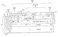
- FIG. 1is an example of a portion of a semiconductor containing a lateral DMOS device having a strained silicon layer, in accordance with a preferred embodiment of the invention
- FIG. 2is a flowchart of an exemplary method for forming a DMOS device having a strained silicon portion in accordance with a preferred embodiment of the invention
- FIG. 3is an example of a portion of a semiconductor comprising a vertical DMOS device having a strained silicon portion, in accordance with a preferred embodiment of the invention
- FIG. 4is an example of a portion of a semiconductor comprising a trench DMOS device having a strained silicon layer, in accordance with a preferred embodiment of the invention
- FIG. 5is a flowchart of an exemplary method for forming trench DMOS devices, in accordance with a preferred embodiment of the invention.
- FIG. 6is an example of a portion of a semiconductor comprising an LDMOS device on silicon on insulator (SOI), having a strained silicon layer, in accordance with a preferred embodiment of the invention.
- SOIsilicon on insulator
- FIGS. 7 and 8are examples of portions of a semiconductor comprising an LDMOS device having strained silicon portions, in accordance with a preferred embodiment of the invention.
- the strained silicon portionsare generally formed in at least the drift region of a DMOS device.
- Techniques for forming conventional DMOS devicesare well known in the art. Consequently, emphasis is placed herein on exemplary techniques for forming strained silicon portions in DMOS devices and DMOS devices containing the strained silicon portions.
- the DMOS devices described hereinare devices using electrons as carriers. However, the benefits described above are also applicable to devices using holes as carriers.
- Semiconductor portion 100comprises a separating trench 145 , a substrate 140 , an epitaxial (“epi”) layer 135 , a lattice mismatch material layer 130 , a strained silicon layer 125 , a body 185 , an enhancement region 180 , a source region 106 , two diffusion areas 165 and 170 , a drain region 121 , an insulator 115 , a gate 110 , a source conductor 107 and a drain conductor 122 .
- Trench 145comprises an insulator or polysilicon layer 190 and a shorting layer 195 .
- a lateral DMOS (LDMOS) device 160Formed in semiconductor portion 100 is a lateral DMOS (LDMOS) device 160 , which comprises a source 105 , the gate 110 and its insulator 115 , a drift region 150 , the drain 120 , and the body 185 .
- Substrate 140 , epitaxial layer 135 , lattice mismatch material 130 , and strained silicon layer 125will be called a semiconductor region 101 herein.
- the semiconductor region 101has a top surface 102 and a bottom surface 103 , both of which are generally planarized through techniques such as chemical-mechanical polishing (CMP).
- CMPchemical-mechanical polishing
- the gate 110slightly overlaps the source region 106 but is spaced some distance apart from, and does not overlap, the drain region 121 .
- overlapis not meant to imply that a feature has to be “over” a region. Instead, the term “overlap” means that a vertical or horizontal line or plane (relative to top surface 102 or bottom surface 103 ) would, if passed through at least a portion of the feature (e.g., a gate) and at least a portion of a region (e.g., the drain region), intersect.
- FIG. 4illustrated below, illustrates a trench DMOS device where the gate overlaps a source region but the gate is situated vertically in the semiconductor region (e.g., semiconductor region 101 ).
- Source 105comprises the source conductor 107 and source region 106 , which is a highly doped region.
- Drain 120comprises the drain conductor 122 and drain region 121 , which is a highly doped region.
- Insulator 115has a thin portion 116 underlying the gate 110 .
- Drift region 150is a region between gate edge 111 and drain region 121 , and drift region 150 comprises a lightly doped diffusion area 165 and a moderately doped diffusion area 170 .
- the drift region 150is characterized, in a forward conduction mode of LDMOS device 160 , by carriers drifting under the influence of an electric field.
- the drift region 150is formed via the two diffusion areas 165 and 170 .
- FIG. 1there are certain devices that use multiple layers to form a drift region. For instance, some devices use a drift region formed by using a superjunction, as described in T. Fujihara et al., “Simulated Superior Performance of Semiconductor Superjunction Devices,” Proc. of the 10th Int'l Symp. on Power Semiconductor Devices & ICs, 423 (1998), the disclosure of which is hereby incorporated by reference.
- Substrate 140is, in this example, a highly doped substrate.
- Epitaxial layer 135is a lightly doped layer that is formed on substrate 140 , generally by growing the epitaxial layer 135 .
- Lattice mismatch material layer 130is, in this example, silicon germanium, Si 1-x Ge x , where “x” is chosen in order to create certain spacing for the lattice structure in the strained silicon layer 125 .
- Lattice mismatch material layer 130is generally deposited on epitaxial layer 135 through techniques such as ultrahigh vacuum chemical-vapor deposition (CVD) and molecular beam epitaxy (MBE).
- strained silicon layer 125is also generally formed via CVD.
- a typical strained silicon layerhas about eighty percent higher carrier mobility and about ten percent higher saturation velocity for carriers than a conventional silicon layer.
- Techniques for forming a silicon germanium layer 130 and a strained silicon layer 125are known to those skilled in the art. For instance, AmberWave Systems, located at 13 Garabedian Drive, Salem, N.H., 03079, has developed suitable techniques for forming these layers.
- a reference that discusses strained silicon layers in terms of CMOSis K. Rim et al., “Strained Silicon NMOSFETs for High Performance CMOS Technology,” Symp. on VLSI Technology, 59 (2001), the disclosure of which is hereby incorporated by reference.
- body 185is a distinguishing feature of DMOS devices, as compared to MOS devices.
- Body 185is a medium doped region that at least partially underlies gate 110 and, therefore, at least partially fills channel 186 .
- Body 185is generally doped one to two orders of magnitude higher than the epitaxial layer 135 .
- a DMOS devicesuch as LDMOS 160 , generally uses two diffusions in order to form, with one diffusion, body 185 and, with a second diffusion, source region 106 and drain region 121 .
- Enhancement region 180is optional but is beneficial to reduce the occurrence of latch up due to a parasitic bipolar junction formed by source region 106 , body 185 , and diffusion areas 165 , 170 .
- the shorting layer 195is beneficial in order to (1) connect the top source region 106 to the heavily doped substrate 140 and (2) to short the parasitic bipolar junction formed by source region 106 , body 185 , and diffusion areas 165 , 170 .
- Diffusion areas 165 and 170are part of drift region 150 .
- current from channel 186passes through the diffusion areas 165 and 170 and to drain region 121 . Consequently, the increased mobility and saturation velocity, as compared with a conventional silicon layer, of the strained silicon layer 125 provide maximal benefit when used in drift region 150 .
- the strained silicon layer 125has a thickness 171 .
- the lattice mismatch material layer 130has a thickness 131 .
- the thickness 171 of the strained silicon layer 125is varied depending on application. For example, a higher power LDMOS 160 might have a thicker strained silicon layer 125 , in order to totally encompass the diffusion areas 165 , 170 .
- the lattice mismatch material layer 130has a thickness 131 .
- This thickness 131is generally a predetermined thickness in order to create an appropriate lattice structure at boundary 137 of the strained silicon layer 125 , where the appropriate lattice structure is defined by the ratio between silicon and germanium in the Si 1-x Ge x lattice mismatch material layer 130 at the boundary 137 .
- the thickness 131generally runs from a few hundred angstroms to about two thousand angstroms.
- the ratio between silicon and germanium, as defined by the variable “x”is varied as the lattice mismatch material layer 130 is grown from boundary 136 to boundary 137 of epitaxial layer 135 .
- AmberWave Systemshas disclosed grading techniques in order to produce such a variance in ratio.
- the thickness 131 of the lattice mismatch material 130is usually greater than the thickness 171 of the strained silicon layer 125 .
- diffusion areas 165 , 170can be diffused into the lattice mismatch material 130 , but this is less preferable than having the diffusion areas 165 , 170 be relegated above boundary 137 .
- a carrier transit path between the source region 106 and drain region 121is as follows: carriers are emitted from the source region 106 , travel through a channel defined in the body 185 , travel through the drift region 150 , and to the drain region 121 .
- the carrier transit pathcan include the source region 106 and drain region 121 .
- an exemplary method 200is shown for forming an LDMOS 160 having a strained silicon portion, which, in this example, is a strained silicon layer 125 .
- Method 200is performed during LDMOS processing, which is well known in the art.
- preprocessingis performed.
- Such preprocessingcan include doping of substrate 140 , if not already doped, formation of the epitaxial layer 135 , and chemical-mechanical polishing (CMP), if needed, of the epitaxial layer 135 in order to form a smooth boundary 136 .
- CMPchemical-mechanical polishing
- the lattice mismatch material layer 130is formed through processes known to those skilled in the art.
- a silicon germanium layermay be formed by ultrahigh vacuum CVD and MBE.
- the lattice mismatch material layer 130may also be processed, such as through CMP, in order to prepare the boundary 137 for formation of strained silicon layer 125 .
- AmberWave Systemshas developed suitable CMP techniques for a lattice mismatch material layer 130 layer of silicon germanium.
- the strained silicon layer 125is formed and, if desired, processed.
- Strained silicon layer 125may be formed, as is known in the art, through a variety of techniques such as CVD and MBE.
- the strained silicon layer 125may also be processed, if desired, through such techniques as CMP.
- step 240LDMOS processing is continued in order, for example, to define body 185 , enhancement region 180 , source 105 , drain 120 , diffusion areas 165 and 170 , gate 110 , insulator 115 , and trench 145 .
- method 200allows an LDMOS device 160 to be created having a strained silicon layer 125 .
- silicon germaniumis and will be described herein as the lattice mismatch material layer 130
- other lattice mismatch materialsmay be used, such as silicon carbide.
- the strained silicon layer 125would be placed onto the epitaxial layer 135 , without the intervening lattice mismatch material layer 130 .
- epitaxial deposition of siliconcould be continued over a silicon-germanium layer until the strained silicon layer is thick enough to remove.
- DMOS devices having strained silicon portionsmay be integrated with other devices, such as CMOS devices or bipolar junction transistor devices. Such integration generally occurs as part of an integrated circuit. The processing to create the CMOS or bipolar devices may occur before, during, or after the steps of method 200 .
- VDMOS device 360comprises a source 305 coupled to a drain region 320 through a substrate 350 , bodies 385 and 386 , an accumulation layer 326 , source regions 315 and 317 , and conductor 310 .
- the accumulation layer 326is formed by gate 312 , which is formed over insulator 311 .
- Insulator 311also surrounds gate 312 in this example.
- Conductor 310is formed over insulator 311 .
- the regions 316 and 318are used to reduce latch up.
- the drain region 320 , substrate 350 , lattice mismatch material layer 330 , and strained silicon layer 325will be referred to as semiconductor region 301 herein, which has a top surface 302 and a bottom surface 303 . It should be noted that an additional substrate layer (not shown) may also exist below bottom surface 303 , in certain embodiments.
- a carrier transit pathis as follows: carriers pass from the highly doped source region 315 , through a surface (e.g., near insulator 311 ) of body 385 and body 385 , through channel lattice mismatch material 330 , through substrate 350 , and to drain region 320 .
- a similar carrier transit pathcan occur from source region 317 to drain region 320 .
- Drain region 320could be a highly doped region formed, for instance, on a backside of a semiconductor wafer. Alternatively, the drain region 320 can be formed as a buried layer in substrate 350 . Generally, a drain would be formed by contacting the drain region 320 with a conductive lead of some type.
- a drift regionlies between insulator 311 and drain region 320 (e.g., the area comprising the strained silicon layer 325 , the lattice mismatch material layer 330 , and the substrate 350 between the bodies 385 , 386 ).
- the strained silicon layer 325is, as in the VDMOS 160 of FIG. 1, formed over a lattice mismatch material layer 330 .
- the gate 312overlaps source region 315 and is spaced some distance from the drain region 320 .
- Body 385partially overlaps gate 312 .
- Method 200 of FIG. 2can be used to form the VDMOS device 360 .
- the substrate 350may be prepared through known techniques (see step 210 of FIG. 2 ), the lattice mismatch material layer 330 can be formed and processed through techniques as disclosed in step 220 of FIG. 2, and the strained silicon layer 325 can be formed and processed as disclosed in step 230 of FIG. 2 .
- the semiconductor portion 300can be completed, as described in step 240 of FIG. 2, through techniques known to those skilled in the art.
- the gate 312 and underlying insulator 311can be formed, then the bodies 385 , 386 can be formed, the region 318 formed, and the insulator 311 and conductor 310 formed.
- Trench DMOS device 460comprises a source 415 , a gate 416 , insulator 411 , body 486 , substrate 450 , and drain 420 .
- Source 415comprises conductor 410 and source region 415 .
- a carrier transit pathis as follows: carriers flow through highly doped source region 415 , through body 486 , through substrate 410 , and to drain 420 .
- Highly doped region 472is used to reduce latch up.
- Highly doped region 473can also be used as part of a source 415 when gate 417 is used.
- the drain region 420can be a highly doped region formed on the backside of a semiconductor wafer or could be a buried layer. Additionally, the drain region 420 would generally be coupled to a conductor (not shown) in order to form a drain (not shown).
- the drain region 420 , substrate 450 , body 485 , and other diffusion regions (e.g., source region 415 )will be referred to as semiconductor region 401 herein, which has a top surface 402 and a bottom surface 403 . It should be noted that an additional substrate layer (not shown) may also exist below bottom surface 403 , in certain embodiments.
- the gate 426overlaps the source region 415 and is spaced some distance from the drain region 420 . Additionally, the body 486 overlaps the gate 416 .
- the drift regioncomprises the area beneath the body 486 and to the drain 420 .
- the strained silicon layer 425is formed over lattice mismatch material 430 , and both are formed in this example in trenches 480 , 481 .
- an exemplary method 500is shown for forming the trench DMOS devices shown in FIG. S.
- Method 500begins in step 510 when preprocessing is performed.
- the step of preprocessingcould be a simple as using a cleaning solution in order to prepare the semiconductor portion 400 for subsequent steps.
- the bodies 485 , 486could be doped.
- a hard maskis formed on the semiconductor portion 400 and is patterned in order to define trenches 480 , 481 .
- the hard maskis formed through known techniques and could comprise oxide or oxide-nitride, for instance.
- trenchessuch as trenches 480 , 481 , are etched through known techniques such as Reactive Ion Etching (RIE).
- RIEReactive Ion Etching
- a lattice mismatch material layere.g., lattice mismatch material layer 430
- silicon germaniumis formed.
- a strained silicon layeris formed. The lattice mismatch material layer and strained silicon layer are formed through techniques such as those previously described.
- step 535the lattice mismatch material layer and strained silicon layer are removed except in the trenches. This could occur by using an etch specific to silicon germanium, which would preferentially remove silicon germanium, yet such an etch should leave the trenches 480 , 481 intact.
- step 540the hard mask is removed through, for instance, reactive ion etching (RIE) or wet etching. It should be noted that both steps 535 and 540 may be performed through RIE or wet etching.
- RIEreactive ion etching
- step 545DMOS processing is continued in order to define trenches 482 , 483 , add insulator 411 , define trenches for gates 416 , 417 , perform doping of regions 415 , 473 , and 472 , and define conductors 410 .
- stepsare known to those skilled in the art.
- LDMOS device 680 on silicon-on-insulatoris shown on semiconductor portion 600 .
- Semiconductor portion 600comprises the LDMOS device 680 , a highly doped region 612 , an oxide layer 660 , and a silicon substrate 670 .
- LDMOS device 680comprises a source 610 , a gate 620 formed over an insulator 640 , a body 655 , and a drain 630 .
- Source 610comprises a highly doped region 611 and will generally comprise a conductor (not shown) coupled to the highly doped region 611 .
- the drain 630comprises a lightly doped drain (LDD) 632 and a highly doped region 631 , and will generally comprise a conductor (not shown) coupled to the region 631 .
- LDDlightly doped drain
- the substrate 670 , oxide layer 660 and strained silicon layer 650will be referred to as semiconductor region 601 herein, which also has a top surface 602 and a bottom surface 603 .
- the strained silicon layer 650exists above and coupled to the oxide 660 .
- AmberWave Systemshas a process to separate a strained silicon layer from an underlying silicon germanium layer and to bond the separated strained silicon layer to an oxide layer.
- LDMOS device 780is shown formed on a semiconductor portion 700 .
- the semiconductor portion 700comprises the LDMOS device 780 , a highly doped region 712 , and substrate 770 .
- LDMOS device 780comprises a source 710 , a gate 720 formed over an insulator 740 , a body 755 , and a drain 730 .
- Source 710comprises a highly doped source region 711 and will generally comprise a conductor (not shown) coupled to the highly doped source region 711 .
- the drain 730comprises an LDD 732 and a highly doped region 731 , and will generally comprise a conductor (not shown) coupled to the region 731 .
- the substrate 770 , body 755 , lattice mismatch material 790 , strained silicon layer 791 , and diffusion areas(e.g., source region 711 and highly doped region 712 ) will be referred to as a semiconductor region 701 , which has a top surface 702 .
- a strained silicon region 791is formed over the lattice mismatch material region 790 .
- the strained silicon region 791fills the drift region 750 .
- the strained silicon region 791may be formed by the following technique.
- a hard mask(not shown) can be formed over substrate 770 and patterned so that the area 772 (to the right of edge 771 ) is uncovered. The area 772 is etched using conventional techniques.
- a lattice mismatch material layeris formed, as is a strained silicon layer.
- the strained silicon layer and lattice mismatch material layerare removed from the semiconductor portion 700 except in area 772 by selective etching. Then, the hard mask is removed through conventional techniques.
- the lattice mismatch material, strained silicon layer and hard maskcan be removed via CMP.
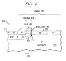
- a semiconductor portion 800is shown having an LDMOS device 780 with a strained silicon region 791 .
- the strained silicon portion 791 and lattice mismatch material 790are formed in the channel region 850 .
- the strained silicon region 791may be formed by the following technique.
- a hard mask(not shown) can be formed over substrate 770 and patterned so that the area 772 is uncovered. The area 772 is etched using conventional techniques.
- a lattice mismatch material layeris formed, as is a strained silicon layer.
- the strained silicon layer and lattice mismatch material layerare removed from the semiconductor portion 700 except in area 772 by selective etching.
- the hard maskis removed through conventional techniques.
- the lattice mismatch material, strained silicon layer and hard maskcan be removed via CMP.
- strained silicon portionscan, as compared to conventional DMOS devices, increase the transconductance, lower the on-resistance, lower the knee-voltage, and increase the saturation current. It is beneficial that a strained silicon portion be placed in the drift region of a DMOS device, as the increases in the mobility and saturation velocity due to strained silicon in the drift region generally provide these advantages. As described above, however, strained silicon may also be applied to other areas of a DMOS device, such as the channel and source and drain regions. Any carrier transmit path where carriers flow from source region to drain region in a DMOS device should benefit from strained silicon, although benefits of strained silicon might be highest when the strained silicon is placed in the drift region.
Landscapes
- Insulated Gate Type Field-Effect Transistor (AREA)
Abstract
Description
Claims (20)
Priority Applications (1)
| Application Number | Priority Date | Filing Date | Title |
|---|---|---|---|
| US10/382,142US6828628B2 (en) | 2003-03-05 | 2003-03-05 | Diffused MOS devices with strained silicon portions and methods for forming same |
Applications Claiming Priority (1)
| Application Number | Priority Date | Filing Date | Title |
|---|---|---|---|
| US10/382,142US6828628B2 (en) | 2003-03-05 | 2003-03-05 | Diffused MOS devices with strained silicon portions and methods for forming same |
Publications (2)
| Publication Number | Publication Date |
|---|---|
| US20040173846A1 US20040173846A1 (en) | 2004-09-09 |
| US6828628B2true US6828628B2 (en) | 2004-12-07 |
Family
ID=32926821
Family Applications (1)
| Application Number | Title | Priority Date | Filing Date |
|---|---|---|---|
| US10/382,142Expired - LifetimeUS6828628B2 (en) | 2003-03-05 | 2003-03-05 | Diffused MOS devices with strained silicon portions and methods for forming same |
Country Status (1)
| Country | Link |
|---|---|
| US (1) | US6828628B2 (en) |
Cited By (11)
| Publication number | Priority date | Publication date | Assignee | Title |
|---|---|---|---|---|
| US20050093097A1 (en)* | 2003-10-30 | 2005-05-05 | Baiocchi Frank A. | Enhanced substrate contact for a semiconductor device |
| US20050253191A1 (en)* | 2004-05-03 | 2005-11-17 | Sameer Pendharkar | Robust DEMOS transistors and method for making the same |
| US20060105528A1 (en)* | 2004-11-17 | 2006-05-18 | Young Kyun Cho | High voltage mosfet having Si/SiGe heterojunction structure and method of manufacturing the same |
| US20070096206A1 (en)* | 2005-11-03 | 2007-05-03 | International Business Machines Corporation | Gate electrode stress control for finfet performance enhancement |
| US20070096170A1 (en)* | 2005-11-02 | 2007-05-03 | International Business Machines Corporation | Low modulus spacers for channel stress enhancement |
| US20070120154A1 (en)* | 2005-11-30 | 2007-05-31 | International Business Machines Corporation | Finfet structure with multiply stressed gate electrode |
| US20070122965A1 (en)* | 2005-09-29 | 2007-05-31 | International Business Machines Corporation | Stress engineering using dual pad nitride with selective soi device architecture |
| US20070152274A1 (en)* | 2003-12-12 | 2007-07-05 | Rohm Co., Ltd. | Semiconductor device |
| US20080014690A1 (en)* | 2006-07-17 | 2008-01-17 | Chartered Semiconductor Manufacturing, Ltd | LDMOS using a combination of enhanced dielectric stress layer and dummy gates |
| US20080050877A1 (en)* | 2006-08-25 | 2008-02-28 | De Fresart Edouard D | Superjunction trench device and method |
| US7863197B2 (en) | 2006-01-09 | 2011-01-04 | International Business Machines Corporation | Method of forming a cross-section hourglass shaped channel region for charge carrier mobility modification |
Families Citing this family (22)
| Publication number | Priority date | Publication date | Assignee | Title |
|---|---|---|---|---|
| US6909151B2 (en) | 2003-06-27 | 2005-06-21 | Intel Corporation | Nonplanar device with stress incorporation layer and method of fabrication |
| US6989567B2 (en)* | 2003-10-03 | 2006-01-24 | Infineon Technologies North America Corp. | LDMOS transistor |
| US7042009B2 (en) | 2004-06-30 | 2006-05-09 | Intel Corporation | High mobility tri-gate devices and methods of fabrication |
| US7348284B2 (en) | 2004-08-10 | 2008-03-25 | Intel Corporation | Non-planar pMOS structure with a strained channel region and an integrated strained CMOS flow |
| US7422946B2 (en) | 2004-09-29 | 2008-09-09 | Intel Corporation | Independently accessed double-gate and tri-gate transistors in same process flow |
| US20060086977A1 (en) | 2004-10-25 | 2006-04-27 | Uday Shah | Nonplanar device with thinned lower body portion and method of fabrication |
| US7193279B2 (en)* | 2005-01-18 | 2007-03-20 | Intel Corporation | Non-planar MOS structure with a strained channel region |
| US7518196B2 (en) | 2005-02-23 | 2009-04-14 | Intel Corporation | Field effect transistor with narrow bandgap source and drain regions and method of fabrication |
| US7402875B2 (en) | 2005-08-17 | 2008-07-22 | Intel Corporation | Lateral undercut of metal gate in SOI device |
| JP4907920B2 (en)* | 2005-08-18 | 2012-04-04 | 株式会社東芝 | Semiconductor device and manufacturing method thereof |
| US7825465B2 (en)* | 2007-12-13 | 2010-11-02 | Fairchild Semiconductor Corporation | Structure and method for forming field effect transistor with low resistance channel region |
| US8362566B2 (en) | 2008-06-23 | 2013-01-29 | Intel Corporation | Stress in trigate devices using complimentary gate fill materials |
| US8237195B2 (en)* | 2008-09-29 | 2012-08-07 | Fairchild Semiconductor Corporation | Power MOSFET having a strained channel in a semiconductor heterostructure on metal substrate |
| US8193559B2 (en) | 2009-01-27 | 2012-06-05 | Infineon Technologies Austria Ag | Monolithic semiconductor switches and method for manufacturing |
| US7943955B2 (en)* | 2009-01-27 | 2011-05-17 | Infineon Technologies Austria Ag | Monolithic semiconductor switches and method for manufacturing |
| CN101819998B (en)* | 2010-04-29 | 2011-11-16 | 哈尔滨工程大学 | High voltage low power consumption SOI LDMOS transistor having strained silicon structure |
| US8921933B2 (en) | 2011-05-19 | 2014-12-30 | Macronix International Co., Ltd. | Semiconductor structure and method for operating the same |
| DE102011108651B4 (en) | 2011-07-26 | 2019-10-17 | Austriamicrosystems Ag | High-voltage transistor device and manufacturing method |
| US8753948B2 (en)* | 2011-10-31 | 2014-06-17 | Freescale Semiconductor, Inc. | Methods of forming laterally diffused metal oxide semiconductor transistors for radio frequency power amplifiers |
| US9461164B2 (en) | 2013-09-16 | 2016-10-04 | Infineon Technologies Ag | Semiconductor device and method of manufacturing the same |
| US9123801B2 (en)* | 2013-09-16 | 2015-09-01 | Infineon Technologies Ag | Semiconductor device, integrated circuit and method of manufacturing a semiconductor device |
| CN103745998B (en)* | 2013-12-31 | 2016-10-26 | 上海新傲科技股份有限公司 | Groove power field-effect transistor |
Citations (5)
| Publication number | Priority date | Publication date | Assignee | Title |
|---|---|---|---|---|
| US5776812A (en) | 1994-03-30 | 1998-07-07 | Nippondenso Co., Ltd. | Manufacturing method of semiconductor device |
| US5780324A (en) | 1994-03-30 | 1998-07-14 | Denso Corporation | Method of manufacturing a vertical semiconductor device |
| US6107661A (en) | 1995-09-29 | 2000-08-22 | Nippondenso Co., Ltd. | Semiconductor device and method of manufacturing same |
| US20020030227A1 (en)* | 2000-01-20 | 2002-03-14 | Bulsara Mayank T. | Strained-silicon diffused metal oxide semiconductor field effect transistors |
| US20020125471A1 (en)* | 2000-12-04 | 2002-09-12 | Fitzgerald Eugene A. | CMOS inverter circuits utilizing strained silicon surface channel MOSFETS |
- 2003
- 2003-03-05USUS10/382,142patent/US6828628B2/ennot_activeExpired - Lifetime
Patent Citations (5)
| Publication number | Priority date | Publication date | Assignee | Title |
|---|---|---|---|---|
| US5776812A (en) | 1994-03-30 | 1998-07-07 | Nippondenso Co., Ltd. | Manufacturing method of semiconductor device |
| US5780324A (en) | 1994-03-30 | 1998-07-14 | Denso Corporation | Method of manufacturing a vertical semiconductor device |
| US6107661A (en) | 1995-09-29 | 2000-08-22 | Nippondenso Co., Ltd. | Semiconductor device and method of manufacturing same |
| US20020030227A1 (en)* | 2000-01-20 | 2002-03-14 | Bulsara Mayank T. | Strained-silicon diffused metal oxide semiconductor field effect transistors |
| US20020125471A1 (en)* | 2000-12-04 | 2002-09-12 | Fitzgerald Eugene A. | CMOS inverter circuits utilizing strained silicon surface channel MOSFETS |
Non-Patent Citations (6)
| Title |
|---|
| "Amberwave and Aixtron to Develop CVD Equipment for SiGe and Strained Si," http://www.compoundsemiconductor.net/articles/news (May 17, 2002). |
| Huang et al., "Carrier Mobility Enhancement in Strained Si-On-Insulator Fabricated by Wafer Bonding," Symp. on VLSI Technology, 59 (2001). |
| Lammers, D., "AmberWave Strained-Silicon Process Removes Troublesome SiGe Layer," Electronic Engineering Times (Oct. 21, 2002). |
| Murphy, T., "Intel Strains to Pull Ahead-Process Technology Disclosure Raises Eyebrows" Electronic News, p. 14 (Aug. 19, 2002). |
| Murphy, T., "Intel Strains to Pull Ahead—Process Technology Disclosure Raises Eyebrows" Electronic News, p. 14 (Aug. 19, 2002). |
| Rim et al., "Strained Silicon NMOSFETs for High Performance CMOS Technology," Symp. on VLSI Technology, 59 (2001). |
Cited By (25)
| Publication number | Priority date | Publication date | Assignee | Title |
|---|---|---|---|---|
| US6987052B2 (en)* | 2003-10-30 | 2006-01-17 | Agere Systems Inc. | Method for making enhanced substrate contact for a semiconductor device |
| US20050093097A1 (en)* | 2003-10-30 | 2005-05-05 | Baiocchi Frank A. | Enhanced substrate contact for a semiconductor device |
| US20070152274A1 (en)* | 2003-12-12 | 2007-07-05 | Rohm Co., Ltd. | Semiconductor device |
| US20050253191A1 (en)* | 2004-05-03 | 2005-11-17 | Sameer Pendharkar | Robust DEMOS transistors and method for making the same |
| US7238986B2 (en)* | 2004-05-03 | 2007-07-03 | Texas Instruments Incorporated | Robust DEMOS transistors and method for making the same |
| US20060105528A1 (en)* | 2004-11-17 | 2006-05-18 | Young Kyun Cho | High voltage mosfet having Si/SiGe heterojunction structure and method of manufacturing the same |
| US7233018B2 (en)* | 2004-11-17 | 2007-06-19 | Electronics And Telecommunications Research Institute | High voltage MOSFET having Si/SiGe heterojuction structure and method of manufacturing the same |
| US7550364B2 (en) | 2005-09-29 | 2009-06-23 | International Business Machines Corporation | Stress engineering using dual pad nitride with selective SOI device architecture |
| US20070122965A1 (en)* | 2005-09-29 | 2007-05-31 | International Business Machines Corporation | Stress engineering using dual pad nitride with selective soi device architecture |
| US20070096170A1 (en)* | 2005-11-02 | 2007-05-03 | International Business Machines Corporation | Low modulus spacers for channel stress enhancement |
| US20070096206A1 (en)* | 2005-11-03 | 2007-05-03 | International Business Machines Corporation | Gate electrode stress control for finfet performance enhancement |
| US7655511B2 (en) | 2005-11-03 | 2010-02-02 | International Business Machines Corporation | Gate electrode stress control for finFET performance enhancement |
| US20070120154A1 (en)* | 2005-11-30 | 2007-05-31 | International Business Machines Corporation | Finfet structure with multiply stressed gate electrode |
| US7564081B2 (en) | 2005-11-30 | 2009-07-21 | International Business Machines Corporation | finFET structure with multiply stressed gate electrode |
| US7863197B2 (en) | 2006-01-09 | 2011-01-04 | International Business Machines Corporation | Method of forming a cross-section hourglass shaped channel region for charge carrier mobility modification |
| US20080014690A1 (en)* | 2006-07-17 | 2008-01-17 | Chartered Semiconductor Manufacturing, Ltd | LDMOS using a combination of enhanced dielectric stress layer and dummy gates |
| US7824968B2 (en) | 2006-07-17 | 2010-11-02 | Chartered Semiconductor Manufacturing Ltd | LDMOS using a combination of enhanced dielectric stress layer and dummy gates |
| US20110042743A1 (en)* | 2006-07-17 | 2011-02-24 | Globalfoundries Singapore Pte. Ltd. | LDMOS Using A Combination of Enhanced Dielectric Stress Layer and Dummy Gates |
| US8334567B2 (en) | 2006-07-17 | 2012-12-18 | Globalfoundries Singapore Pte. Ltd. | LDMOS using a combination of enhanced dielectric stress layer and dummy gates |
| WO2008024572A3 (en)* | 2006-08-25 | 2008-04-17 | Freescale Semiconductor Inc | Superjunction trench device and method |
| US20080050877A1 (en)* | 2006-08-25 | 2008-02-28 | De Fresart Edouard D | Superjunction trench device and method |
| US7598517B2 (en) | 2006-08-25 | 2009-10-06 | Freescale Semiconductor, Inc. | Superjunction trench device and method |
| US20090286372A1 (en)* | 2006-08-25 | 2009-11-19 | Freescale Semiconductor, Inc. | Superjunction trench device formation methods |
| US7833858B2 (en) | 2006-08-25 | 2010-11-16 | Freesscale Semiconductor, Inc. | Superjunction trench device formation methods |
| KR101387992B1 (en)* | 2006-08-25 | 2014-04-22 | 프리스케일 세미컨덕터, 인크. | Superjunction trench device and method |
Also Published As
| Publication number | Publication date |
|---|---|
| US20040173846A1 (en) | 2004-09-09 |
Similar Documents
| Publication | Publication Date | Title |
|---|---|---|
| US6828628B2 (en) | Diffused MOS devices with strained silicon portions and methods for forming same | |
| US9166039B2 (en) | Lateral transistor component and method for producing same | |
| KR101115091B1 (en) | Semiconductor structure with different lattice constant materials and method for forming the same | |
| US6709982B1 (en) | Double spacer FinFET formation | |
| US9117850B2 (en) | Method and system for a gallium nitride vertical JFET with self-aligned source and gate | |
| US6955969B2 (en) | Method of growing as a channel region to reduce source/drain junction capacitance | |
| CN101233605B (en) | Methods for fabricating a stressed MOS device | |
| US20070102761A1 (en) | Semiconductor device and method of fabricating the same | |
| US20070023828A1 (en) | Semiconductor device and method of manufacturing the same | |
| US8716078B2 (en) | Method and system for a gallium nitride vertical JFET with self-aligned gate metallization | |
| WO2008112508A1 (en) | Short channel lv, mv, and hv cmos devices | |
| US10211336B2 (en) | LDMOS transistor structures and integrated circuits including LDMOS transistor structures | |
| US20230215916A1 (en) | Circuit Structure and Method for Reducing Electronic Noises | |
| US8841708B2 (en) | Method and system for a GAN vertical JFET with self-aligned source metallization | |
| US10749023B2 (en) | Vertical transistor with extended drain region | |
| US20160284561A1 (en) | Method of Manufacturing a Semiconductor Device Having a Buried Channel/Body Zone | |
| CN102637741B (en) | The resonant tunneling device of using metal oxide semiconductor processing | |
| US7479422B2 (en) | Semiconductor device with stressors and method therefor | |
| US20240413239A1 (en) | Ldmos nanosheet transistor | |
| US8779525B2 (en) | Method for growing strain-inducing materials in CMOS circuits in a gate first flow | |
| CN114823841A (en) | Semiconductor structure and forming method thereof | |
| JPH1022501A (en) | Semiconductor device and manufacturing method thereof | |
| US20250142946A1 (en) | Backside isolation of semiconductor structures | |
| US20250107242A1 (en) | Semiconductor structure and method for forming the same | |
| US12446307B2 (en) | Structure and method of forming spacers on unfaceted raised source/drain regions |
Legal Events
| Date | Code | Title | Description |
|---|---|---|---|
| AS | Assignment | Owner name:AGERE SYSTEMS INC., PENNSYLVANIA Free format text:ASSIGNMENT OF ASSIGNORS INTEREST;ASSIGNORS:HERGENROTHER, JOHN;SHIBIB, MUHAMMED AYMAN;XIE, ZHIJIAN;AND OTHERS;REEL/FRAME:013851/0125;SIGNING DATES FROM 20030303 TO 20030304 | |
| STCF | Information on status: patent grant | Free format text:PATENTED CASE | |
| CC | Certificate of correction | ||
| FPAY | Fee payment | Year of fee payment:4 | |
| FPAY | Fee payment | Year of fee payment:8 | |
| AS | Assignment | Owner name:DEUTSCHE BANK AG NEW YORK BRANCH, AS COLLATERAL AG Free format text:PATENT SECURITY AGREEMENT;ASSIGNORS:LSI CORPORATION;AGERE SYSTEMS LLC;REEL/FRAME:032856/0031 Effective date:20140506 | |
| AS | Assignment | Owner name:AVAGO TECHNOLOGIES GENERAL IP (SINGAPORE) PTE. LTD Free format text:ASSIGNMENT OF ASSIGNORS INTEREST;ASSIGNOR:AGERE SYSTEMS LLC;REEL/FRAME:035365/0634 Effective date:20140804 | |
| AS | Assignment | Owner name:LSI CORPORATION, CALIFORNIA Free format text:TERMINATION AND RELEASE OF SECURITY INTEREST IN PATENT RIGHTS (RELEASES RF 032856-0031);ASSIGNOR:DEUTSCHE BANK AG NEW YORK BRANCH, AS COLLATERAL AGENT;REEL/FRAME:037684/0039 Effective date:20160201 Owner name:AGERE SYSTEMS LLC, PENNSYLVANIA Free format text:TERMINATION AND RELEASE OF SECURITY INTEREST IN PATENT RIGHTS (RELEASES RF 032856-0031);ASSIGNOR:DEUTSCHE BANK AG NEW YORK BRANCH, AS COLLATERAL AGENT;REEL/FRAME:037684/0039 Effective date:20160201 | |
| AS | Assignment | Owner name:BANK OF AMERICA, N.A., AS COLLATERAL AGENT, NORTH CAROLINA Free format text:PATENT SECURITY AGREEMENT;ASSIGNOR:AVAGO TECHNOLOGIES GENERAL IP (SINGAPORE) PTE. LTD.;REEL/FRAME:037808/0001 Effective date:20160201 Owner name:BANK OF AMERICA, N.A., AS COLLATERAL AGENT, NORTH Free format text:PATENT SECURITY AGREEMENT;ASSIGNOR:AVAGO TECHNOLOGIES GENERAL IP (SINGAPORE) PTE. LTD.;REEL/FRAME:037808/0001 Effective date:20160201 | |
| FPAY | Fee payment | Year of fee payment:12 | |
| AS | Assignment | Owner name:AVAGO TECHNOLOGIES GENERAL IP (SINGAPORE) PTE. LTD., SINGAPORE Free format text:TERMINATION AND RELEASE OF SECURITY INTEREST IN PATENTS;ASSIGNOR:BANK OF AMERICA, N.A., AS COLLATERAL AGENT;REEL/FRAME:041710/0001 Effective date:20170119 Owner name:AVAGO TECHNOLOGIES GENERAL IP (SINGAPORE) PTE. LTD Free format text:TERMINATION AND RELEASE OF SECURITY INTEREST IN PATENTS;ASSIGNOR:BANK OF AMERICA, N.A., AS COLLATERAL AGENT;REEL/FRAME:041710/0001 Effective date:20170119 | |
| AS | Assignment | Owner name:BELL SEMICONDUCTOR, LLC, ILLINOIS Free format text:ASSIGNMENT OF ASSIGNORS INTEREST;ASSIGNORS:AVAGO TECHNOLOGIES GENERAL IP (SINGAPORE) PTE. LTD.;BROADCOM CORPORATION;REEL/FRAME:044886/0608 Effective date:20171208 | |
| AS | Assignment | Owner name:CORTLAND CAPITAL MARKET SERVICES LLC, AS COLLATERA Free format text:SECURITY INTEREST;ASSIGNORS:HILCO PATENT ACQUISITION 56, LLC;BELL SEMICONDUCTOR, LLC;BELL NORTHERN RESEARCH, LLC;REEL/FRAME:045216/0020 Effective date:20180124 | |
| AS | Assignment | Owner name:BELL NORTHERN RESEARCH, LLC, ILLINOIS Free format text:RELEASE BY SECURED PARTY;ASSIGNOR:CORTLAND CAPITAL MARKET SERVICES LLC;REEL/FRAME:059720/0719 Effective date:20220401 Owner name:BELL SEMICONDUCTOR, LLC, ILLINOIS Free format text:RELEASE BY SECURED PARTY;ASSIGNOR:CORTLAND CAPITAL MARKET SERVICES LLC;REEL/FRAME:059720/0719 Effective date:20220401 Owner name:HILCO PATENT ACQUISITION 56, LLC, ILLINOIS Free format text:RELEASE BY SECURED PARTY;ASSIGNOR:CORTLAND CAPITAL MARKET SERVICES LLC;REEL/FRAME:059720/0719 Effective date:20220401 |