US6827978B2 - Deposition of tungsten films - Google Patents
Deposition of tungsten filmsDownload PDFInfo
- Publication number
- US6827978B2 US6827978B2US10/074,898US7489802AUS6827978B2US 6827978 B2US6827978 B2US 6827978B2US 7489802 AUS7489802 AUS 7489802AUS 6827978 B2US6827978 B2US 6827978B2
- Authority
- US
- United States
- Prior art keywords
- tungsten
- layers
- deposited
- range
- layer
- Prior art date
- Legal status (The legal status is an assumption and is not a legal conclusion. Google has not performed a legal analysis and makes no representation as to the accuracy of the status listed.)
- Expired - Fee Related, expires
Links
- WFKWXMTUELFFGS-UHFFFAOYSA-NtungstenChemical group[W]WFKWXMTUELFFGS-UHFFFAOYSA-N0.000titleclaimsabstractdescription281
- 229910052721tungstenInorganic materials0.000titleclaimsabstractdescription281
- 239000010937tungstenSubstances0.000titleclaimsabstractdescription281
- 230000008021depositionEffects0.000titledescription41
- 238000000034methodMethods0.000claimsabstractdescription153
- 230000008569processEffects0.000claimsabstractdescription101
- 230000006911nucleationEffects0.000claimsabstractdescription87
- 238000010899nucleationMethods0.000claimsabstractdescription87
- 239000002243precursorSubstances0.000claimsabstractdescription65
- 239000000758substrateSubstances0.000claimsabstractdescription52
- 239000002131composite materialSubstances0.000claimsabstractdescription49
- 238000000151depositionMethods0.000claimsdescription54
- NXHILIPIEUBEPD-UHFFFAOYSA-Htungsten hexafluorideChemical groupF[W](F)(F)(F)(F)FNXHILIPIEUBEPD-UHFFFAOYSA-H0.000claimsdescription37
- BLRPTPMANUNPDV-UHFFFAOYSA-NSilaneChemical compound[SiH4]BLRPTPMANUNPDV-UHFFFAOYSA-N0.000claimsdescription12
- UORVGPXVDQYIDP-UHFFFAOYSA-NboraneChemical compoundBUORVGPXVDQYIDP-UHFFFAOYSA-N0.000claimsdescription9
- 229910000077silaneInorganic materials0.000claimsdescription8
- 230000004888barrier functionEffects0.000claimsdescription7
- 238000001465metallisationMethods0.000claimsdescription7
- 229910000085boraneInorganic materials0.000claimsdescription5
- FQNHWXHRAUXLFU-UHFFFAOYSA-Ncarbon monoxide;tungstenChemical group[W].[O+]#[C-].[O+]#[C-].[O+]#[C-].[O+]#[C-].[O+]#[C-].[O+]#[C-]FQNHWXHRAUXLFU-UHFFFAOYSA-N0.000claimsdescription5
- MROCJMGDEKINLD-UHFFFAOYSA-NdichlorosilaneChemical compoundCl[SiH2]ClMROCJMGDEKINLD-UHFFFAOYSA-N0.000claimsdescription4
- PZPGRFITIJYNEJ-UHFFFAOYSA-NdisilaneChemical compound[SiH3][SiH3]PZPGRFITIJYNEJ-UHFFFAOYSA-N0.000claimsdescription4
- AIGRXSNSLVJMEA-FQEVSTJZSA-Nethoxy-(4-nitrophenoxy)-phenyl-sulfanylidene-$l^{5}-phosphaneChemical compoundO([P@@](=S)(OCC)C=1C=CC=CC=1)C1=CC=C([N+]([O-])=O)C=C1AIGRXSNSLVJMEA-FQEVSTJZSA-N0.000claimsdescription4
- 229910052581Si3N4Inorganic materials0.000claimsdescription2
- VYPSYNLAJGMNEJ-UHFFFAOYSA-NSilicium dioxideChemical compoundO=[Si]=OVYPSYNLAJGMNEJ-UHFFFAOYSA-N0.000claimsdescription2
- NRTOMJZYCJJWKI-UHFFFAOYSA-NTitanium nitrideChemical compound[Ti]#NNRTOMJZYCJJWKI-UHFFFAOYSA-N0.000claimsdescription2
- 239000011810insulating materialSubstances0.000claimsdescription2
- HQVNEWCFYHHQES-UHFFFAOYSA-Nsilicon nitrideChemical compoundN12[Si]34N5[Si]62N3[Si]51N64HQVNEWCFYHHQES-UHFFFAOYSA-N0.000claimsdescription2
- 229910052814silicon oxideInorganic materials0.000claimsdescription2
- MZLGASXMSKOWSE-UHFFFAOYSA-Ntantalum nitrideChemical compound[Ta]#NMZLGASXMSKOWSE-UHFFFAOYSA-N0.000claimsdescription2
- 239000000203mixtureSubstances0.000claims2
- 238000005229chemical vapour depositionMethods0.000abstractdescription31
- 238000005137deposition processMethods0.000abstractdescription8
- 239000010410layerSubstances0.000description113
- 239000007789gasSubstances0.000description87
- NJPPVKZQTLUDBO-UHFFFAOYSA-NnovaluronChemical compoundC1=C(Cl)C(OC(F)(F)C(OC(F)(F)F)F)=CC=C1NC(=O)NC(=O)C1=C(F)C=CC=C1FNJPPVKZQTLUDBO-UHFFFAOYSA-N0.000description43
- 239000012159carrier gasSubstances0.000description25
- XKRFYHLGVUSROY-UHFFFAOYSA-NArgonChemical compound[Ar]XKRFYHLGVUSROY-UHFFFAOYSA-N0.000description20
- 229910052786argonInorganic materials0.000description10
- 238000004519manufacturing processMethods0.000description10
- 238000010926purgeMethods0.000description8
- 230000003746surface roughnessEffects0.000description8
- 239000000463materialSubstances0.000description6
- 230000015572biosynthetic processEffects0.000description5
- ZOCHARZZJNPSEU-UHFFFAOYSA-NdiboronChemical compoundB#BZOCHARZZJNPSEU-UHFFFAOYSA-N0.000description5
- 230000005684electric fieldEffects0.000description5
- 238000001459lithographyMethods0.000description5
- 239000003989dielectric materialSubstances0.000description4
- XUIMIQQOPSSXEZ-UHFFFAOYSA-NSiliconChemical compound[Si]XUIMIQQOPSSXEZ-UHFFFAOYSA-N0.000description3
- 238000010438heat treatmentMethods0.000description3
- 238000000623plasma-assisted chemical vapour depositionMethods0.000description3
- 239000000376reactantSubstances0.000description3
- 229910052710siliconInorganic materials0.000description3
- 239000010703siliconSubstances0.000description3
- 238000006243chemical reactionMethods0.000description2
- 239000010949copperSubstances0.000description2
- 238000006073displacement reactionMethods0.000description2
- -1for exampleSubstances0.000description2
- 230000007246mechanismEffects0.000description2
- 230000009257reactivityEffects0.000description2
- 239000002356single layerSubstances0.000description2
- 238000001179sorption measurementMethods0.000description2
- JBRZTFJDHDCESZ-UHFFFAOYSA-NAsGaChemical compound[As]#[Ga]JBRZTFJDHDCESZ-UHFFFAOYSA-N0.000description1
- IJGRMHOSHXDMSA-UHFFFAOYSA-NAtomic nitrogenChemical compoundN#NIJGRMHOSHXDMSA-UHFFFAOYSA-N0.000description1
- RYGMFSIKBFXOCR-UHFFFAOYSA-NCopperChemical compound[Cu]RYGMFSIKBFXOCR-UHFFFAOYSA-N0.000description1
- 229910003915SiCl2H2Inorganic materials0.000description1
- 230000004913activationEffects0.000description1
- WYEMLYFITZORAB-UHFFFAOYSA-NboscalidChemical compoundC1=CC(Cl)=CC=C1C1=CC=CC=C1NC(=O)C1=CC=CN=C1ClWYEMLYFITZORAB-UHFFFAOYSA-N0.000description1
- 239000006227byproductSubstances0.000description1
- 238000009833condensationMethods0.000description1
- 230000005494condensationEffects0.000description1
- 229910052802copperInorganic materials0.000description1
- 230000008878couplingEffects0.000description1
- 238000010168coupling processMethods0.000description1
- 238000005859coupling reactionMethods0.000description1
- 238000009792diffusion processMethods0.000description1
- 230000000694effectsEffects0.000description1
- 230000002708enhancing effectEffects0.000description1
- 238000005530etchingMethods0.000description1
- 230000005284excitationEffects0.000description1
- 229910052732germaniumInorganic materials0.000description1
- GNPVGFCGXDBREM-UHFFFAOYSA-Ngermanium atomChemical compound[Ge]GNPVGFCGXDBREM-UHFFFAOYSA-N0.000description1
- 239000001307heliumSubstances0.000description1
- 229910052734heliumInorganic materials0.000description1
- SWQJXJOGLNCZEY-UHFFFAOYSA-Nhelium atomChemical compound[He]SWQJXJOGLNCZEY-UHFFFAOYSA-N0.000description1
- 239000001257hydrogenSubstances0.000description1
- 229910052739hydrogenInorganic materials0.000description1
- 125000004435hydrogen atomChemical class[H]*0.000description1
- 239000004065semiconductorSubstances0.000description1
- 238000003860storageMethods0.000description1
Images


Classifications
- C—CHEMISTRY; METALLURGY
- C23—COATING METALLIC MATERIAL; COATING MATERIAL WITH METALLIC MATERIAL; CHEMICAL SURFACE TREATMENT; DIFFUSION TREATMENT OF METALLIC MATERIAL; COATING BY VACUUM EVAPORATION, BY SPUTTERING, BY ION IMPLANTATION OR BY CHEMICAL VAPOUR DEPOSITION, IN GENERAL; INHIBITING CORROSION OF METALLIC MATERIAL OR INCRUSTATION IN GENERAL
- C23C—COATING METALLIC MATERIAL; COATING MATERIAL WITH METALLIC MATERIAL; SURFACE TREATMENT OF METALLIC MATERIAL BY DIFFUSION INTO THE SURFACE, BY CHEMICAL CONVERSION OR SUBSTITUTION; COATING BY VACUUM EVAPORATION, BY SPUTTERING, BY ION IMPLANTATION OR BY CHEMICAL VAPOUR DEPOSITION, IN GENERAL
- C23C16/00—Chemical coating by decomposition of gaseous compounds, without leaving reaction products of surface material in the coating, i.e. chemical vapour deposition [CVD] processes
- C23C16/44—Chemical coating by decomposition of gaseous compounds, without leaving reaction products of surface material in the coating, i.e. chemical vapour deposition [CVD] processes characterised by the method of coating
- C23C16/455—Chemical coating by decomposition of gaseous compounds, without leaving reaction products of surface material in the coating, i.e. chemical vapour deposition [CVD] processes characterised by the method of coating characterised by the method used for introducing gases into reaction chamber or for modifying gas flows in reaction chamber
- C23C16/45523—Pulsed gas flow or change of composition over time
- C23C16/45525—Atomic layer deposition [ALD]
- C—CHEMISTRY; METALLURGY
- C23—COATING METALLIC MATERIAL; COATING MATERIAL WITH METALLIC MATERIAL; CHEMICAL SURFACE TREATMENT; DIFFUSION TREATMENT OF METALLIC MATERIAL; COATING BY VACUUM EVAPORATION, BY SPUTTERING, BY ION IMPLANTATION OR BY CHEMICAL VAPOUR DEPOSITION, IN GENERAL; INHIBITING CORROSION OF METALLIC MATERIAL OR INCRUSTATION IN GENERAL
- C23C—COATING METALLIC MATERIAL; COATING MATERIAL WITH METALLIC MATERIAL; SURFACE TREATMENT OF METALLIC MATERIAL BY DIFFUSION INTO THE SURFACE, BY CHEMICAL CONVERSION OR SUBSTITUTION; COATING BY VACUUM EVAPORATION, BY SPUTTERING, BY ION IMPLANTATION OR BY CHEMICAL VAPOUR DEPOSITION, IN GENERAL
- C23C16/00—Chemical coating by decomposition of gaseous compounds, without leaving reaction products of surface material in the coating, i.e. chemical vapour deposition [CVD] processes
- C23C16/02—Pretreatment of the material to be coated
- C23C16/0272—Deposition of sub-layers, e.g. to promote the adhesion of the main coating
- C23C16/0281—Deposition of sub-layers, e.g. to promote the adhesion of the main coating of metallic sub-layers
- C—CHEMISTRY; METALLURGY
- C23—COATING METALLIC MATERIAL; COATING MATERIAL WITH METALLIC MATERIAL; CHEMICAL SURFACE TREATMENT; DIFFUSION TREATMENT OF METALLIC MATERIAL; COATING BY VACUUM EVAPORATION, BY SPUTTERING, BY ION IMPLANTATION OR BY CHEMICAL VAPOUR DEPOSITION, IN GENERAL; INHIBITING CORROSION OF METALLIC MATERIAL OR INCRUSTATION IN GENERAL
- C23C—COATING METALLIC MATERIAL; COATING MATERIAL WITH METALLIC MATERIAL; SURFACE TREATMENT OF METALLIC MATERIAL BY DIFFUSION INTO THE SURFACE, BY CHEMICAL CONVERSION OR SUBSTITUTION; COATING BY VACUUM EVAPORATION, BY SPUTTERING, BY ION IMPLANTATION OR BY CHEMICAL VAPOUR DEPOSITION, IN GENERAL
- C23C16/00—Chemical coating by decomposition of gaseous compounds, without leaving reaction products of surface material in the coating, i.e. chemical vapour deposition [CVD] processes
- C23C16/06—Chemical coating by decomposition of gaseous compounds, without leaving reaction products of surface material in the coating, i.e. chemical vapour deposition [CVD] processes characterised by the deposition of metallic material
- C23C16/08—Chemical coating by decomposition of gaseous compounds, without leaving reaction products of surface material in the coating, i.e. chemical vapour deposition [CVD] processes characterised by the deposition of metallic material from metal halides
- C23C16/14—Deposition of only one other metal element
- H—ELECTRICITY
- H01—ELECTRIC ELEMENTS
- H01L—SEMICONDUCTOR DEVICES NOT COVERED BY CLASS H10
- H01L21/00—Processes or apparatus adapted for the manufacture or treatment of semiconductor or solid state devices or of parts thereof
- H01L21/02—Manufacture or treatment of semiconductor devices or of parts thereof
- H01L21/04—Manufacture or treatment of semiconductor devices or of parts thereof the devices having potential barriers, e.g. a PN junction, depletion layer or carrier concentration layer
- H01L21/18—Manufacture or treatment of semiconductor devices or of parts thereof the devices having potential barriers, e.g. a PN junction, depletion layer or carrier concentration layer the devices having semiconductor bodies comprising elements of Group IV of the Periodic Table or AIIIBV compounds with or without impurities, e.g. doping materials
- H01L21/28—Manufacture of electrodes on semiconductor bodies using processes or apparatus not provided for in groups H01L21/20 - H01L21/268
- H01L21/283—Deposition of conductive or insulating materials for electrodes conducting electric current
- H01L21/285—Deposition of conductive or insulating materials for electrodes conducting electric current from a gas or vapour, e.g. condensation
- H01L21/28506—Deposition of conductive or insulating materials for electrodes conducting electric current from a gas or vapour, e.g. condensation of conductive layers
- H01L21/28512—Deposition of conductive or insulating materials for electrodes conducting electric current from a gas or vapour, e.g. condensation of conductive layers on semiconductor bodies comprising elements of Group IV of the Periodic Table
- H01L21/28556—Deposition of conductive or insulating materials for electrodes conducting electric current from a gas or vapour, e.g. condensation of conductive layers on semiconductor bodies comprising elements of Group IV of the Periodic Table by chemical means, e.g. CVD, LPCVD, PECVD, laser CVD
- H01L21/28562—Selective deposition
- H—ELECTRICITY
- H01—ELECTRIC ELEMENTS
- H01L—SEMICONDUCTOR DEVICES NOT COVERED BY CLASS H10
- H01L21/00—Processes or apparatus adapted for the manufacture or treatment of semiconductor or solid state devices or of parts thereof
- H01L21/02—Manufacture or treatment of semiconductor devices or of parts thereof
- H01L21/04—Manufacture or treatment of semiconductor devices or of parts thereof the devices having potential barriers, e.g. a PN junction, depletion layer or carrier concentration layer
- H01L21/18—Manufacture or treatment of semiconductor devices or of parts thereof the devices having potential barriers, e.g. a PN junction, depletion layer or carrier concentration layer the devices having semiconductor bodies comprising elements of Group IV of the Periodic Table or AIIIBV compounds with or without impurities, e.g. doping materials
- H01L21/28—Manufacture of electrodes on semiconductor bodies using processes or apparatus not provided for in groups H01L21/20 - H01L21/268
- H01L21/283—Deposition of conductive or insulating materials for electrodes conducting electric current
- H01L21/285—Deposition of conductive or insulating materials for electrodes conducting electric current from a gas or vapour, e.g. condensation
- H01L21/28506—Deposition of conductive or insulating materials for electrodes conducting electric current from a gas or vapour, e.g. condensation of conductive layers
- H01L21/28512—Deposition of conductive or insulating materials for electrodes conducting electric current from a gas or vapour, e.g. condensation of conductive layers on semiconductor bodies comprising elements of Group IV of the Periodic Table
- H01L21/28568—Deposition of conductive or insulating materials for electrodes conducting electric current from a gas or vapour, e.g. condensation of conductive layers on semiconductor bodies comprising elements of Group IV of the Periodic Table the conductive layers comprising transition metals
- H—ELECTRICITY
- H01—ELECTRIC ELEMENTS
- H01L—SEMICONDUCTOR DEVICES NOT COVERED BY CLASS H10
- H01L21/00—Processes or apparatus adapted for the manufacture or treatment of semiconductor or solid state devices or of parts thereof
- H01L21/70—Manufacture or treatment of devices consisting of a plurality of solid state components formed in or on a common substrate or of parts thereof; Manufacture of integrated circuit devices or of parts thereof
- H01L21/71—Manufacture of specific parts of devices defined in group H01L21/70
- H01L21/768—Applying interconnections to be used for carrying current between separate components within a device comprising conductors and dielectrics
- H01L21/76838—Applying interconnections to be used for carrying current between separate components within a device comprising conductors and dielectrics characterised by the formation and the after-treatment of the conductors
- H01L21/76877—Filling of holes, grooves or trenches, e.g. vias, with conductive material
Definitions
- Embodiments of the present inventiongenerally relate to a method of tungsten film deposition and, more particularly, to a method of forming a tungsten film having good film morphology.
- tungsten (W) filmsare often used as contact metallization or plug metallization for interconnect schemes. Tungsten (W) films may also be used as a diffusion barrier for copper (Cu) in various metallization schemes.
- the tungsten (W) filmsare typically composite films comprising a thin tungsten (W) nucleation layer (thickness of about 50 ⁇ to about 150 ⁇ ) and a thicker bulk tungsten layer (thickness of about 500 ⁇ to about 2000 ⁇ ) formed thereover.
- tungsten films comprised of a thin tungsten nucleation layer and a thick bulk tungsten layertend to have poor film morphology.
- the morphology of a filmrefers to its surface roughness, and grain structure.
- tungsten (W) filmscomprising a thin tungsten nucleation layer and a thick bulk tungsten layer typically have large grain sizes (e.g., grain sizes of greater than about 10 nm/rms). Large grain sizes produce rough surfaces, which are undesirable for subsequent lithography steps performed thereover.
- a method of forming a composite tungsten film on a substratecomprises sequentially deposited tungsten nucleation layers and tungsten bulk layers. Each of the tungsten nucleation layers and the tungsten bulk layers have a thickness less than about 300 ⁇ . The tungsten nucleation layers and the tungsten bulk layers are formed one over the other until a desired thickness for the composite tungsten film is achieved. The resulting composite tungsten film exhibits good film morphology.
- the tungsten nucleation layersmay be formed using a cyclical deposition process by alternately adsorbing a tungsten-containing precursor and a reducing gas on the substrate.
- the tungsten bulk layersmay be formed using a chemical vapor deposition (CVD) process by thermally decomposing a tungsten-containing precursor.
- the composite tungsten filmis compatible with integrated circuit fabrication processes.
- the composite tungsten filmmay be used as word and/or bit line metallization to read and write data to memory cell devices.
- a preferred process sequenceincludes providing a substrate having a word and/or bit line pattern defined in a dielectric material layer.
- the word and/or bit line pattern defined in the dielectric materialincludes a barrier layer thereon.
- a composite tungsten filmcomprising sequentially deposited tungsten nucleation layers and tungsten bulk layers, each having a thickness less than about 300 ⁇ , are formed one over the other on the barrier layer until a desired thickness for the composite tungsten film is achieved.
- FIG. 1depicts a schematic illustration of an apparatus that can be used for the practice of embodiments described herein;
- FIG. 2depicts a schematic cross-sectional view of a process chamber that can be used to perform a cyclical deposition process described herein;
- FIG. 3depicts a schematic cross-sectional view of a process chamber that can be used to perform a chemical vapor deposition (CVD) process described herein;
- CVDchemical vapor deposition
- FIG. 4illustrates a process sequence for tungsten composite film formation
- FIG. 5illustrates a process sequence for tungsten nucleation layer formation using cyclical deposition techniques according to one embodiment described herein;
- FIG. 6illustrates a process sequence for tungsten nucleation layer formation using cyclical deposition techniques according to an alternate embodiment described herein;
- FIG. 7depicts surface roughness data for composite tungsten films of the present invention and thick chemical vapor deposition (CVD) tungsten films;
- FIGS. 8A-8Billustrate schematic cross-sectional views of an integrated circuit at different stages of fabrication incorporating word and/or bit-line structures.
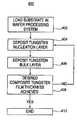
- FIG. 1is a schematic representation of a wafer processing system 35 that can be used to perform integrated circuit fabrication in accordance with embodiments described herein.
- the wafer processing system 35typically comprises process chambers 36 , 38 , 40 , 41 , transfer chamber 50 , load-lock chambers 52 , a factory interface 46 , a microprocessor controller (not shown), along with other hardware components such as power supplies (not shown) and vacuum pumps (not shown).
- An example of such a wafer processing system 35is an ENDURA SL system, available from Applied Materials, Inc., Santa Clara, Calif.
- the wafer processing system 35includes a transfer chamber 50 containing two transfer robots 49 , 51 .
- the transfer chamber 50is coupled to the factory interface 46 via load-lock chambers 52 .
- Substrates(not shown) are loaded into the wafer processing system 35 through factory interface 46 .
- a factory interface robot 48moves the substrates from the factory interface 46 into the load-lock chambers 52 .
- Transfer chamber 50is a coupled to a cluster of process chambers 36 , 38 , 40 , 41 .
- the transfer robots 49 , 51move the substrates between one or more of the process chambers 36 , 38 , 40 , 41 .
- process chambers 36 , 38 , 40 , 41are used to perform various integrated circuit fabrication sequences.
- process chambers 36 , 38 , 40 , 41may include cyclical deposition chambers as well as chemical vapor deposition (CVD) chambers, among others.
- CVDchemical vapor deposition
- FIG. 2depicts a schematic cross-sectional view of a process chamber 36 of wafer processing system 35 that can be used to perform a cyclical deposition process in accordance with embodiments described herein.
- the process chamber 36generally houses a wafer support pedestal 148 , which is used to support a substrate (not shown).
- the wafer support pedestal 148is movable in a vertical direction inside the process chamber 36 using a displacement mechanism 148 a.
- the substratecan be heated to some desired temperature prior to or during deposition.
- the wafer support pedestal 148may be heated using an embedded heater element 152 a .
- the wafer support pedestal 148may be resistively heated by applying an electric current from an AC power supply 152 to the heater element 152 a .
- the substrate(not shown) is, in turn, heated by the pedestal 148 .
- the wafer support pedestal 148may be heated using radiant heaters, such as, for example, lamps.
- a temperature sensor 150 asuch as a thermocouple, is also embedded in the wafer support pedestal 148 to monitor the temperature of the pedestal 148 in a conventional manner. The measured temperature is used in a feedback loop to control the AC power supply 152 for the heating element 152 a , such that the substrate temperature can be maintained or controlled at a desired temperature which is suitable for the particular process application.
- a vacuum pump 118is used to evacuate the process chamber 36 and to maintain the pressure inside the process chamber 36 .
- a gas manifold 134through which process gases are introduced into the process chamber 36 , is located above the wafer support pedestal 148 .
- the gas manifold 134is connected to a gas panel (not shown), which controls and supplies various process gases to the process chamber 36 .
- Proper control and regulation of the gas flows to the gas manifold 134are performed by mass flow controllers (not shown) and a microprocessor controller 170 .
- the gas manifold 134allows process gases to be introduced and uniformly distributed in the process chamber 36 . Additionally, the gas manifold 134 may optionally be heated to prevent condensation of any reactive gases within the manifold.
- the gas manifold 134includes a plurality of electronic control valves (not shown).
- the electronic control valves as used hereinrefer to any control valve capable of providing rapid and precise gas flow to the process chamber 36 with valve open and close cycles of less than about 1-2 seconds, and more preferably less than about 0.1 second.
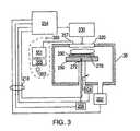
- FIG. 3depicts a schematic cross-sectional view of a chemical vapor deposition (CVD) process chamber 38 of wafer processing system 35 .
- CVDchemical vapor deposition
- An example of such a CVD chamber 38is a WxZTM chamber, commercially available from Applied Materials, Inc., Santa Clara, Calif.
- the CVD chamber 38generally houses a wafer support pedestal 250 , which is used to support a substrate 290 .
- the wafer support pedestal 250is movable in a vertical direction inside the CVD chamber 38 using a displacement mechanism (not shown).
- the substrate 290can be heated to some desired temperature prior to or during deposition.
- the wafer support pedestal 250may be heated by an embedded heater element 270 .
- the wafer support pedestal 250may be resistively heated by applying an electric current from an AC power supply 206 to the heater element 270 .
- the substrate 290is, in turn, heated by the pedestal 250 .
- the wafer support pedestal 250is optionally heated using radiant heat (not shown).
- a temperature sensor 272such as a thermocouple, may also be embedded in the wafer support pedestal 250 to monitor the temperature of the pedestal 250 in a conventional manner. The measured temperature is used in a feedback loop to control the AC power supply 206 for the heating element 270 , such that the substrate temperature can be maintained or controlled at a desired temperature which is suitable for the particular process application.
- a vacuum pump 202is used to evacuate the CVD chamber 38 and to maintain the proper gas flows and pressures inside the CVD chamber 38 .
- a showerhead 220through which process gases are introduced into the CVD chamber 38 , is located above the wafer support pedestal 250 .
- the showerhead 220is connected to a gas panel 230 , which controls and supplies various process gases provided to the CVD chamber 38 .
- Proper control and regulation of the gas flows through the gas panel 230is performed by mass flow controllers (not shown) and a microprocessor controller 254 .
- the showerhead 220allows process gases from the gas panel 230 to be uniformly introduced and distributed in the CVD chamber 38 .
- the CVD chamber 38may comprise additional components for enhancing layer deposition on the substrate 290 .
- the showerhead 220 and wafer support pedestal 250may also form a pair of spaced apart electrodes. When an electric field is generated between these electrodes, the process gases introduced into the CVD chamber 38 may be ignited into a plasma.
- the electric fieldis generated by coupling the wafer support pedestal 250 to a source of radio frequency (RF) power (not shown) through a matching network (not shown).
- RFradio frequency
- the RF power source and matching networkmay be coupled to the showerhead 220 , or coupled to both the showerhead 220 and the wafer support pedestal 250 .
- Plasma enhanced chemical vapor deposition (PECVD) techniquespromote excitation and/or disassociation of the reactant gases by the application of the electric field to the reaction zone near the substrate surface, creating a plasma of reactive species.
- the reactivity of the species in the plasmareduces the energy required for a chemical reaction to take place, in effect lowering the required temperature for such PECVD processes.
- a remote plasma source 350may be coupled to the CVD process chamber 38 to provide a remote plasma thereto.
- the remote plasma source 350includes a gas supply 353 , a gas flow controller 355 , a plasma chamber 351 , and a chamber inlet 357 .
- the gas flow controller 355controls the flow of process gas from the gas supply 353 to the plasma chamber 351 .
- a remote plasmamay be generated by applying an electric field to the process gas in the plasma chamber 351 , creating a plasma of reactive species.
- the electric fieldis generated in the plasma chamber 351 using an RF power source (not shown).
- the reactive species generated in the remote plasma source 350may be introduced into CVD process chamber 38 through inlet 357 .
- Process chamber 36 and the CVD process chamber 38 as described aboveare each controlled by a microprocessor controller 170 (FIG. 2 ), 254 (FIG. 3 ).
- the microprocessor controllers 170 , 254may be one of any form of general purpose computer processor (CPU) that can be used in an industrial setting for controlling various chambers and sub-processors.
- the computermay use any suitable memory, such as random access memory, read only memory, floppy disk drive, hard disk, or any other form of digital storage, local or remote.
- Various support circuitsmay be coupled to the CPU for supporting the processor in a conventional manner.
- Software routines as requiredmay be stored in the memory or executed by a second CPU that is remotely located.
- the software routinesare executed to initiate process recipes or sequences.
- the software routineswhen executed, transform the general purpose computer into a specific process computer that controls the chamber operation so that a chamber process is performed.
- software routinesmay be used to precisely control the activation of the electronic control valves for the execution of process sequences according to the present invention.
- the software routinesmay be performed in hardware, as an application specific integrated circuit or other type of hardware implementation, or a combination of software or hardware.
- the composite tungsten filmcomprises sequentially deposited tungsten nucleation layers and tungsten bulk layers. Each of the tungsten nucleation layers and the tungsten bulk layers have a thickness less than about 300 ⁇ . The tungsten nucleation layers and the tungsten bulk layers are formed one over the other until a desired thickness for the composite tungsten layer is achieved. The resulting composite tungsten film exhibits good film morphology.
- FIG. 4illustrates a process sequence 400 detailing the various steps used for the deposition of the composite tungsten film. These steps may be performed in a wafer processing system similar to that described above with reference to FIGS. 1-3.
- a substrateis provided to a wafer processing system.
- the substratemay be for example, a silicon substrate having a word and/or bit line pattern defined in a dielectric material layer.
- a tungsten nucleation layeris formed on the substrate.
- the tungsten nucleation layermay be formed in a deposition chamber similar to that described above with respect to FIG. 2 .
- the thickness for the tungsten nucleation layeris variable depending on the device structure to be fabricated. Typically, the thickness for the tungsten nucleation layer is less than about 100 ⁇ , preferably between about 15 ⁇ to about 50 ⁇ .
- FIG. 5illustrates an embodiment of a process sequence 500 according to the present invention detailing the various steps used for the deposition of the tungsten nucleation layer utilizing a constant carrier gas flow.
- a substrateis provided to a process chamber.
- the substratemay be for example, a silicon substrate ready for bit and/or word-line metallization during a dynamic random access memory (DRAM) fabrication process.
- the process chamber conditionssuch as, for example, the temperature and pressure are adjusted to enhance the adsorption of the process gases on the substrate.
- the substrateshould be maintained at a temperature between about 200° C. and 400° C. at a process chamber pressure of between about 1 torr and about 10 torr.
- Carrier gasesmay be selected so as to also act as a purge gas for removal of volatile reactants and/or by-products from the process chamber.
- Carrier gasessuch as, for example, helium (He), argon (Ar), nitrogen (N 2 ) and hydrogen (H 2 ), and combinations thereof, among others may be used.
- a pulse of a tungsten-containing precursoris added to the carrier gas stream.
- the term pulse as used hereinrefers to a dose of material injected into the process chamber or into the carrier gas stream.
- the pulse of the tungsten-containing precursorlasts for a predetermined time interval.
- the time interval for the pulse of the tungsten-containing precursoris variable depending upon a number of factors such as, for example, the volume capacity of the process chamber employed, the vacuum system coupled thereto and the volatility/reactivity of the reactants used. For example, (1) a large-volume process chamber may lead to a longer time to stabilize the process conditions such as, for example, carrier/purge gas flow and temperature, requiring a longer pulse time; (2) a lower flow rate for the process gas may also lead to a longer time to stabilize the process conditions requiring a longer pulse time; and (3) a lower chamber pressure means that the process gas is evacuated from the process chamber more quickly requiring a longer pulse time.
- the process conditionsare advantageously selected so that a pulse of the tungsten-containing precursor provides a sufficient amount of precursor so that at least a monolayer of the tungsten-containing precursor is adsorbed on the substrate. Thereafter, excess tungsten-containing precursor remaining in the chamber may be removed from the process chamber by the constant carrier gas stream in combination with the vacuum system.
- a pulse of a reducing gasis added to the carrier gas stream.
- the pulse of the reducing gasalso lasts for a predetermined time interval that is variable as described above with reference to the tungsten-containing precursor.
- the time interval for the pulse of the reducing gasshould be long enough for adsorption of at least a monolayer of the reducing gas on the tungsten-containing precursor.
- Steps 504 through 508comprise one embodiment of a deposition cycle for the tungsten nucleation layer.
- a constant flow of the carrier gasis provided to the process chamber modulated by alternating periods of pulsing and non-pulsing where the periods of pulsing alternate between the tungsten-containing precursor and the reducing gas along with the carrier gas stream, while the periods of non-pulsing include only the carrier gas stream.
- the time interval for each of the pulses of the tungsten-containing precursor and the reducing gasmay have the same duration. That is the duration of the pulse of the tungsten-containing precursor may be identical to the duration of the pulse of the reducing gas.
- a time interval (T 1 ) for the pulse of the tungsten-containing precursoris equal to a time interval (T 2 ) for the pulse of the reducing gas.
- the time interval for each of the pulses of the tungsten-containing precursor and the reducing gasmay have different durations. That is the duration of the pulse of the tungsten-containing precursor may be shorter or longer than the duration of the pulse of the reducing gas.
- the time interval (T 1 ) for the pulse of the tungsten-containing precursoris different than the time interval (T 2 ) for the pulse of the reducing gas.
- the periods of non-pulsing between each of the pulses of the tungsten-containing precursor and the reducing gasmay have the same duration. That is, the duration of the period of non-pulsing between each pulse of the tungsten-containing precursor and each pulse of the reducing gas may be identical.
- a time interval (T 3 ) of non-pulsing between the pulse of the tungsten-containing precursor and the pulse of the reducing gasis equal to a time interval (T 4 ) of non-pulsing between the pulse of the reducing gas and the pulse of the tungsten-containing precursor.
- the periods of non-pulsing between each of the pulses of the tungsten-containing precursor and the reducing gasmay have different durations. That is, the duration of the period of non-pulsing between each pulse of the tungsten-containing precursor and each pulse of the reducing gas may be shorter or longer than the duration of the period of non-pulsing between each pulse of the reducing gas and the tungsten-containing precursor.
- a time interval (T 3 ) of non-pulsing between the pulse of the tungsten-containing precursor and the pulse of the reducing gasis different from a time interval (T 4 ) of non-pulsing between the pulse of the reducing gas and the pulse of the tungsten-containing precursor.
- time intervals for each pulse of the tungsten-containing precursor, the reducing gas and the periods of non-pulsing therebetween for each deposition cyclemay have the same duration.
- a time interval (T 1 ) for the pulse of the tungsten-containing precursor, a time interval (T 2 ) for the pulse of the reducing gas, a time interval (T 3 ) of non-pulsing between the pulse of the tungsten-containing precursor and the pulse of the reducing gas and a time interval (T 4 ) of non-pulsing between the pulse of the reducing gas and the pulse of the tungsten-containing precursoreach have the same value for each deposition cycle.
- a time interval (T 1 ) for the pulse of the tungsten-containing precursorhas the same duration as the time interval (T 1 ) for the pulse of the tungsten-containing precursor in subsequent deposition cycles (C 2 . . . C N ).
- the duration of each pulse of the reducing gas as well as the periods of non-pulsing between the pulse of the tungsten-containing precursor and the reducing gas in the first deposition cycle (C 1 )is the same as the duration of each pulse of the reducing gas and the periods of non-pulsing between the pulse of the tungsten-containing precursor and the reducing gas in subsequent deposition cycles (C 2 . . . C N ), respectively.
- the time intervals for at least one pulse of the tungsten-containing precursor, the reducing gas and the periods of non-pulsing therebetween for one or more of the deposition cycles of the tungsten deposition processmay have different durations.
- one or more of the time intervals (T 1 ) for the pulses of the tungsten-containing precursor, the time intervals (T 2 ) for the reducing gas, the time intervals (T 3 ) of non-pulsing between the pulse of the tungsten-containing precursor and the pulse of the reducing gas and the time intervals (T 4 ) of non-pulsing between the pulse of the reducing gas and the pulse of the tungsten-containing precursormay have different values for one or more deposition cycles of the tungsten deposition process.
- the time interval (T 1 ) for the pulse of the tungsten-containing precursormay be longer or shorter than the time interval (T 1 ) for the pulse of the tungsten-containing precursor in subsequent deposition cycles (C 2 . . . C N ).
- the duration of each pulse of the reducing gas and the periods of non-pulsing between the pulse of the tungsten-containing precursor and the reducing gas in deposition cycle (C 1 )may be the same or different then the duration of corresponding pulses of the reducing gas and the periods of non-pulsing between the pulse of the tungsten-containing precursor and the reducing gas in subsequent deposition cycles (C 2 . . . C N ), respectively.
- step 510after each deposition cycle (steps 504 through 508 ) a thickness of tungsten will be formed on the substrate. Depending on specific device requirements, subsequent deposition cycles may be needed to achieve a desired thickness. As such, steps 504 through 508 are repeated until the desired thickness for the tungsten nucleation layer is achieved. Thereafter, when the desired thickness for the tungsten nucleation layer is achieved the process is stopped as indicated by step 512 .
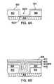
- a tungsten nucleation layer deposition sequence 600includes providing a substrate to the process chamber (step 602 ), providing a first pulse of a purge gas to the process chamber (step 604 ), providing a pulse of a tungsten-containing precursor to the process chamber (step 606 ), providing a second pulse of the purge gas to the process chamber (step 608 ), providing a pulse of the reducing gas to the process chamber (step 610 ), and then repeating steps 604 through 608 , or stopping the deposition process (step 614 ) depending on whether a desired thickness for the tungsten nucleation layer has been achieved (step 612 ).
- the time intervals for each of the pulses of the tungsten-containing precursor, the reducing gas and the purge gasmay have the same or different durations as discussed above with respect to FIG. 5 .
- corresponding time intervals one or more pulses of the tungsten-containing precursor, the reducing gas and the purge gas in one or more of the deposition cycles of the tungsten nucleation deposition processmay have different durations.
- the tungsten nucleation layer deposition cycleis depicted as beginning with a pulse of the tungsten-containing precursor followed by a pulse of the reducing gas.
- the tungsten nucleation layer deposition cyclemay start with a pulse of the reducing gas followed by a pulse of the tungsten-containing precursor.
- Suitable tungsten-containing precursors for forming the tungsten nucleation layermay include for example, tungsten hexafluoride (WF 6 ) and tungsten carbonyl, among others.
- Suitable reducing gasesmay include for example, silane (SiH 4 ), disilane (Si 2 H 6 ), dichlorosilane (SiCl 2 H 2 ), borane (BH 3 ), diborane (B 2 H 6 ), triborane, tetraborane, pentaborane, hexaborane, heptaborane, octaborane, nonaborane, and decaborane, among others.
- One exemplary process of depositing a tungsten nucleation layercomprises sequentially providing pulses of tungsten hexafluoride (WF 6 ) and pulses of diborane (B 2 H 6 ).
- the tungsten hexafluoride (WF 6 )may be provided to an appropriate flow control valve, for example, an electronic control valve, at a flow rate of between about 10 sccm (standard cubic centimeters per minute) and about 400 sccm, preferably between about 20 sccm and about 100 sccm, and thereafter pulsed for about 1 second or less, preferably about 0.2 seconds or less.
- a carrier gas comprising argonis provided along with the tungsten hexafluoride (WF 6 ) at a flow rate between about 250 sccm to about 1000 sccm, preferably between about 500 sccm to about 750 sccm.
- the diborane (B 2 H 6 )may be provided to an appropriate flow control valve, for example, an electronic control valve, at a flow rate of between about 5 sccm and about 150 sccm, preferably between about 5 sccm and about 25 sccm, and thereafter pulsed for about 1 second or less, preferably about 0.2 seconds or less.
- a carrier gas comprising argonis provided along with the diborane at a flow rate between about 250 sccm to about 1000 sccm, preferably between about 500 sccm to about 750 sccm.
- the substratemay be maintained at a temperature between about 250° C. to about 350° C. at a chamber pressure between about 1 torr to about 10 torr.
- Another exemplary process of depositing a tungsten nucleation layercomprises sequentially providing pulses of tungsten hexafluoride (WF 6 ) and pulses of silane (SiH 4 ).
- the tungsten hexafluoride (WF 6 )may be provided to an appropriate flow control valve, for example, an electronic control valve at a flow rate of between about 10 sccm and about 400 sccm, preferably between about 20 sccm and about 100 sccm, and thereafter pulsed for about 1 second or less, preferably about 0.2 seconds or less.
- a carrier gas comprising argonis provided along with the tungsten hexafluoride at a flow rate between about 250 sccm to about 1000 sccm, preferably between 300 sccm to about 500 sccm.
- the silane (SiH 4 )may be provided to an appropriate flow control valve, for example, an electronic control valve, at a flow rate between about 10 sccm to about 500 sccm, preferably between about 50 sccm to about 200 sccm, and thereafter pulsed for about 1 second or less, preferably about 0.2 seconds or less.
- a carrier gas comprising argonis provided along with the silane at a flow rate between about 250 sccm to about 1000 sccm, preferably between about 300 sccm to about 500 sccm.
- a pulse of a purge gas comprising argon at a flow rate between about 300 sccm to about 1000 sccm, preferably between about 500 sccm to about 750 sccm, in pulses of about 1 second or less, preferably about 0.3 seconds or lessis provided between the pulses of the tungsten hexafluoride (WF 6 ) and the pulses of the silane (SiH 4 ).
- the substratemay be maintained at a temperature between about 300° C. to about 400° C. at a chamber pressure between about 1 torr to about 10 torr.
- a tungsten bulk layeris formed thereover.
- the tungsten bulk layermay be formed in a CVD process chamber similar to that described above with respect to FIG. 3 .
- the thickness for the tungsten bulk layeris variable depending on the device structure to be fabricated. Typically, the thickness for the tungsten bulk layer is less than about 300 ⁇ , preferably between about 150 ⁇ to about 250 ⁇ .
- One exemplary process of depositing a tungsten bulk layercomprises thermally decomposing a tungsten-containing precursor, such as for example, tungsten hexafluoride (WF 6 ).
- the tungsten hexafluoride (WF 6 )may be provided at an undiluted flow rate of between about 10 sccm and about 400 sccm, preferably between about 200 sccm and about 250 sccm.
- a carrier gas comprising argonis provided along with the tungsten hexafluoride (WF 6 ) at a flow rate between about 250 sccm to about 1000 sccm, preferably between about 300 sccm to about 650 sccm.
- the substratemay be maintained at a temperature between about 450° C. to about 600° C. at a chamber pressure between about 10 torr to about 30 torr.
- the above process parametersprovide a deposition rate for the tungsten bulk layer in a range of about 10 ⁇ /min to about 100 ⁇ /min when implemented on a 200 mm (millimeter) substrate in a deposition chamber available from Applied Materials, Inc., located in Santa Clara, Calif.
- CVD deposition chambersare within the scope of the invention, and the parameters listed above may vary according to the particular deposition chamber used to form the tungsten bulk layer.
- other deposition chambersmay have a larger (e.g., configured to accommodate 300 mm substrates) or smaller volume, requiring gas flow rates that are larger or smaller than those recited for deposition chambers available from Applied Materials, Inc.
- Other methods for heating substratessuch as, for example, heater lamps may also be used.
- step 408 in FIG. 4after the tungsten bulk layer (step 406 ) is formed on the tungsten nucleation layer (step 404 ) the total thickness of the composite tungsten film is determined. As such, when a desired thickness for the composite tungsten film has not been achieved, steps 404 through 406 are repeated. However, when the desired thickness for the composite tungsten film is achieved, the process is stopped as indicated by step 410 .
- the thickness for the composite tungsten filmis variable depending on the device structure to be fabricated. Typically, the composite tungsten film may have a thickness between about 500 ⁇ to about 3000 ⁇ .
- Alternately depositing thin tungsten bulk layers over tungsten nucleation layersadvantageously forms composite tungsten (W) layers having a smooth film morphology.
- Wcomposite tungsten
- the formation of the thin CVD deposited tungsten bulk layersprevents the tungsten grain sizes from growing too large.
- the tungsten nucleation layers formed by alternately adsorbing monolayers of a tungsten-containing precursor and a reducing gasare believed to stuff grain boundaries on the CVD deposited tungsten bulk layers thereby providing a composite film having a smooth surface morphology.
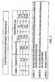
- SAMPLE Billustrates one embodiment of a composite tungsten film comprising sequentially deposited tungsten nucleation layers and tungsten bulk layers.
- the deposition sequenceincludes a thicker first nucleation layer with thinner inter-stage tungsten nucleation layers.
- the deposition sequence for SAMPLE Bincludes a 50 ⁇ tungsten nucleation layer/200 ⁇ tungsten bulk layer/20 ⁇ tungsten nucleation layer/200 ⁇ tungsten bulk layer/20 ⁇ tungsten nucleation layer/200 ⁇ tungsten bulk layer/20 ⁇ tungsten nucleation layer/200 ⁇ tungsten bulk layer/20 ⁇ tungsten nucleation layer/200 ⁇ tungsten bulk layer/20 ⁇ tungsten nucleation layer/200 ⁇ tungsten bulk layer formed one over the other.
- each of the tungsten nucleation layerswas formed by sequentially adsorbing monolayers of tungsten hexafluoride (WF 6 ) and monolayers of diborane (B 2 H 6 ).
- the tungsten hexafluoride (WF 6 )was provided to an electronic control valve at a flow rate of about 50 sccm, and thereafter pulsed for about 0.2 seconds.
- a carrier gas comprising argonwas provided along with the tungsten hexafluoride (WF 6 ) at a flow rate of about 550 sccm.
- the diborane (B 2 H 6 )was provided to an electronic control valve at a flow rate of about 25 sccm, and thereafter pulsed for about 0.2 seconds.
- a carrier gas comprising argonwas provided along with the diborane at a flow rate of 500 sccm.
- the substratewas maintained at a temperature of about 300° C., at a chamber pressure of about 5 torr.
- each of the tungsten bulk layerswas formed by thermally decomposing tungsten hexafluoride (WF 6 ).
- the tungsten hexafluoride (WF 6 )was provided at a flow rate of about 200 sccm.
- a carrier gas comprising argonwas provided along with the tungsten hexafluoride (WF 6 ) at a flow rate of about 500 sccm.
- the substratewas maintained at a temperature of about 550° C., at a chamber pressure of about 10 torr.
- Each of the tungsten nucleation layers and the tungsten bulk layerswere formed by sequentially transferring the substrate between a tungsten nucleation process chamber similar to that described above with respect to FIG. 2 and a CVD process chamber described above with respect to FIG. 3 .
- both the tungsten nucleation layers and the tungsten bulk layersmay be formed in a single process chamber for improved throughput.
- SAMPLE Bhad a surface roughness Ra of about 4.27 nm (nanometers), a root mean square roughness R rms of about 5.39 nm and a maximum roughness R max of about 37.65 nm. Such values for the surface roughness provide a smooth surface morphology for the composite tungsten film that is sufficient for subsequent lithography steps performed thereover.
- SAMPLE Aillustrates another embodiment of a composite tungsten film comprising sequentially deposited tungsten nucleation layers and tungsten bulk layers.
- the deposition sequenceincludes a thicker first and last tungsten nucleation layers with thinner inter-stage tungsten nucleation layers.
- the deposition sequence for SAMPLE Aincludes a 50 ⁇ tungsten nucleation layer/200 ⁇ tungsten bulk layer/20 ⁇ tungsten nucleation layer/200 ⁇ tungsten bulk layer/20 ⁇ tungsten nucleation layer/200 ⁇ tungsten bulk layer/20 ⁇ tungsten nucleation layer/200 ⁇ tungsten bulk layer/20 ⁇ tungsten nucleation layer/200 ⁇ tungsten bulk layer/50 ⁇ tungsten nucleation layer formed one over the other.
- each of the tungsten nucleation layers and the tungsten bulk layerswere formed in separate process chambers according to the process parameters described above with respect to SAMPLE B.
- SAMPLE Ahad a surface roughness Ra of about 4.58 nm, a root mean square roughness R rms of about 5.76 nm and a maximum roughness R max of about 42.74 nm.
- Such values for the surface roughnessprovide a smooth surface morphology for the composite tungsten film that is sufficient for subsequent lithography steps performed thereover.
- SAMPLE Cillustrates a composite tungsten film comprising a single tungsten nucleation layer with a single thick tungsten bulk layer thereon.
- the deposition sequence for SAMPLE Cincludes a 50 ⁇ tungsten nucleation layer/1000 ⁇ tungsten bulk layer.
- the tungsten nucleation layer and the tungsten bulk layerwere each formed in separate process chambers according to the process parameters described above with respect to SAMPLE B.
- SAMPLE Chad a surface roughness Ra of about 9.48 nm and a maximum roughness R max of about 67.09 nm, more than two times rougher than for SAMPLE A and SAMPLE B.
- the surface roughness values for SAMPLE Cprovide a much rougher surface morphology for the composite tungsten film that is insufficient for subsequent lithography steps performed thereover.
- FIGS. 8A-8Billustrate cross-sectional views of a substrate at different stages of a fabrication process incorporating the composite tungsten film of the present invention as word and/or bit line metallization to read and write date to memory cell devices.
- FIG. 8Aillustrates a cross-sectional view of a substrate 800 having a dielectric layer 802 thereon.
- the substrate 800may comprise a semiconductor material such as, for example, silicon (Si), germanium (Ge), or gallium arsenide (GaAs).
- the dielectric materialmay comprise an insulating material such as, for example, silicon oxide or silicon nitride.
- the dielectric layer 802has at least one aperture 802 H formed therein. The at least one aperture 802 H may be formed using conventional lithography and etching techniques.
- the at least one aperture 802 Hmay have a barrier layer 804 thereon.
- the barrier layer 804may comprise for example, titanium nitride (TiN) or tantalum nitride (TaN), among others.
- the barrier layer 804may be formed using conventional deposition techniques.
- a composite tungsten film 806comprising sequentially deposited tungsten nucleation layers 808 and tungsten bulk layers 810 are used to fill the at least one aperture 802 H.
- the composite tungsten film 806is formed using the deposition techniques described above with respect to FIGS. 4-6.
- the resulting composite tungsten filmexhibits good film morphology.
Landscapes
- Chemical & Material Sciences (AREA)
- Engineering & Computer Science (AREA)
- Chemical Kinetics & Catalysis (AREA)
- General Chemical & Material Sciences (AREA)
- Manufacturing & Machinery (AREA)
- Materials Engineering (AREA)
- Microelectronics & Electronic Packaging (AREA)
- Power Engineering (AREA)
- Physics & Mathematics (AREA)
- General Physics & Mathematics (AREA)
- Condensed Matter Physics & Semiconductors (AREA)
- Computer Hardware Design (AREA)
- Mechanical Engineering (AREA)
- Metallurgy (AREA)
- Organic Chemistry (AREA)
- Crystallography & Structural Chemistry (AREA)
- Chemical Vapour Deposition (AREA)
- Electrodes Of Semiconductors (AREA)
Abstract
Description
1. Field of the Invention
Embodiments of the present invention generally relate to a method of tungsten film deposition and, more particularly, to a method of forming a tungsten film having good film morphology.
2. Description of the Related Art
In the manufacture of integrated circuits, tungsten (W) films are often used as contact metallization or plug metallization for interconnect schemes. Tungsten (W) films may also be used as a diffusion barrier for copper (Cu) in various metallization schemes.
The tungsten (W) films are typically composite films comprising a thin tungsten (W) nucleation layer (thickness of about 50 Å to about 150 Å) and a thicker bulk tungsten layer (thickness of about 500 Å to about 2000 Å) formed thereover. However, tungsten films comprised of a thin tungsten nucleation layer and a thick bulk tungsten layer tend to have poor film morphology. The morphology of a film refers to its surface roughness, and grain structure.
For example, tungsten (W) films comprising a thin tungsten nucleation layer and a thick bulk tungsten layer typically have large grain sizes (e.g., grain sizes of greater than about 10 nm/rms). Large grain sizes produce rough surfaces, which are undesirable for subsequent lithography steps performed thereover.
Therefore, a need exists in the art for a method of forming tungsten films having good film morphology.
A method of forming a composite tungsten film on a substrate is provided The composite tungsten film comprises sequentially deposited tungsten nucleation layers and tungsten bulk layers. Each of the tungsten nucleation layers and the tungsten bulk layers have a thickness less than about 300 Å. The tungsten nucleation layers and the tungsten bulk layers are formed one over the other until a desired thickness for the composite tungsten film is achieved. The resulting composite tungsten film exhibits good film morphology.
The tungsten nucleation layers may be formed using a cyclical deposition process by alternately adsorbing a tungsten-containing precursor and a reducing gas on the substrate. The tungsten bulk layers may be formed using a chemical vapor deposition (CVD) process by thermally decomposing a tungsten-containing precursor.
The composite tungsten film is compatible with integrated circuit fabrication processes. In one integrated circuit fabrication process, the composite tungsten film may be used as word and/or bit line metallization to read and write data to memory cell devices. For a word and/or bit line fabrication process, a preferred process sequence includes providing a substrate having a word and/or bit line pattern defined in a dielectric material layer. The word and/or bit line pattern defined in the dielectric material includes a barrier layer thereon. Thereafter, a composite tungsten film comprising sequentially deposited tungsten nucleation layers and tungsten bulk layers, each having a thickness less than about 300 Å, are formed one over the other on the barrier layer until a desired thickness for the composite tungsten film is achieved.
So that the manner in which the above recited features of the present invention are attained and can be understood in detail, a more particular description of the invention, briefly summarized above, may be had by reference to the embodiments thereof which are illustrated in the appended drawings.
It is to be noted, however, that the appended drawings illustrate only typical embodiments of this invention and are therefore not to be considered limiting of its scope, for the invention may admit to other equally effective embodiments.
FIG. 1 depicts a schematic illustration of an apparatus that can be used for the practice of embodiments described herein;
FIG. 2 depicts a schematic cross-sectional view of a process chamber that can be used to perform a cyclical deposition process described herein;
FIG. 3 depicts a schematic cross-sectional view of a process chamber that can be used to perform a chemical vapor deposition (CVD) process described herein;
FIG. 4 illustrates a process sequence for tungsten composite film formation;
FIG. 5 illustrates a process sequence for tungsten nucleation layer formation using cyclical deposition techniques according to one embodiment described herein;
FIG. 6 illustrates a process sequence for tungsten nucleation layer formation using cyclical deposition techniques according to an alternate embodiment described herein;
FIG. 7 depicts surface roughness data for composite tungsten films of the present invention and thick chemical vapor deposition (CVD) tungsten films; and
FIGS. 8A-8B illustrate schematic cross-sectional views of an integrated circuit at different stages of fabrication incorporating word and/or bit-line structures.
FIG. 1 is a schematic representation of awafer processing system 35 that can be used to perform integrated circuit fabrication in accordance with embodiments described herein. Thewafer processing system 35 typically comprisesprocess chambers transfer chamber 50, load-lock chambers 52, afactory interface 46, a microprocessor controller (not shown), along with other hardware components such as power supplies (not shown) and vacuum pumps (not shown). An example of such awafer processing system 35 is an ENDURA SL system, available from Applied Materials, Inc., Santa Clara, Calif.
Details of thewafer processing system 35 are described in commonly assigned U.S. patent application Ser. No. 09/451,628, entitled “Integrated Modular Processing Platform”, filed on Nov. 30, 1999, which is hereby incorporated herein by reference. The salient features of thewafer processing system 35 are briefly described below.
Thewafer processing system 35 includes atransfer chamber 50 containing twotransfer robots transfer chamber 50 is coupled to thefactory interface 46 via load-lock chambers 52. Substrates (not shown) are loaded into thewafer processing system 35 throughfactory interface 46. Afactory interface robot 48 moves the substrates from thefactory interface 46 into the load-lock chambers 52.
Theprocess chambers process chambers
FIG. 2 depicts a schematic cross-sectional view of aprocess chamber 36 ofwafer processing system 35 that can be used to perform a cyclical deposition process in accordance with embodiments described herein. Theprocess chamber 36 generally houses awafer support pedestal 148, which is used to support a substrate (not shown). Thewafer support pedestal 148 is movable in a vertical direction inside theprocess chamber 36 using adisplacement mechanism 148a.
Depending on the specific process, the substrate can be heated to some desired temperature prior to or during deposition. For example, thewafer support pedestal 148 may be heated using an embeddedheater element 152a. Thewafer support pedestal 148 may be resistively heated by applying an electric current from anAC power supply 152 to theheater element 152a. The substrate (not shown) is, in turn, heated by thepedestal 148. Alternatively, thewafer support pedestal 148 may be heated using radiant heaters, such as, for example, lamps.
Atemperature sensor 150a, such as a thermocouple, is also embedded in thewafer support pedestal 148 to monitor the temperature of thepedestal 148 in a conventional manner. The measured temperature is used in a feedback loop to control theAC power supply 152 for theheating element 152a, such that the substrate temperature can be maintained or controlled at a desired temperature which is suitable for the particular process application.
Avacuum pump 118 is used to evacuate theprocess chamber 36 and to maintain the pressure inside theprocess chamber 36. Agas manifold 134, through which process gases are introduced into theprocess chamber 36, is located above thewafer support pedestal 148. Thegas manifold 134 is connected to a gas panel (not shown), which controls and supplies various process gases to theprocess chamber 36.
Proper control and regulation of the gas flows to thegas manifold 134 are performed by mass flow controllers (not shown) and amicroprocessor controller 170. Thegas manifold 134 allows process gases to be introduced and uniformly distributed in theprocess chamber 36. Additionally, thegas manifold 134 may optionally be heated to prevent condensation of any reactive gases within the manifold.
Thegas manifold 134 includes a plurality of electronic control valves (not shown). The electronic control valves as used herein refer to any control valve capable of providing rapid and precise gas flow to theprocess chamber 36 with valve open and close cycles of less than about 1-2 seconds, and more preferably less than about 0.1 second.
FIG. 3 depicts a schematic cross-sectional view of a chemical vapor deposition (CVD)process chamber 38 ofwafer processing system 35. An example of such aCVD chamber 38 is a WxZ™ chamber, commercially available from Applied Materials, Inc., Santa Clara, Calif.
TheCVD chamber 38 generally houses awafer support pedestal 250, which is used to support asubstrate 290. Thewafer support pedestal 250 is movable in a vertical direction inside theCVD chamber 38 using a displacement mechanism (not shown).
Depending on the specific CVD process, thesubstrate 290 can be heated to some desired temperature prior to or during deposition. For example, thewafer support pedestal 250 may be heated by an embeddedheater element 270. Thewafer support pedestal 250 may be resistively heated by applying an electric current from anAC power supply 206 to theheater element 270. Thesubstrate 290 is, in turn, heated by thepedestal 250. Thewafer support pedestal 250 is optionally heated using radiant heat (not shown).
Atemperature sensor 272, such as a thermocouple, may also be embedded in thewafer support pedestal 250 to monitor the temperature of thepedestal 250 in a conventional manner. The measured temperature is used in a feedback loop to control theAC power supply 206 for theheating element 270, such that the substrate temperature can be maintained or controlled at a desired temperature which is suitable for the particular process application.
Avacuum pump 202 is used to evacuate theCVD chamber 38 and to maintain the proper gas flows and pressures inside theCVD chamber 38. Ashowerhead 220, through which process gases are introduced into theCVD chamber 38, is located above thewafer support pedestal 250. Theshowerhead 220 is connected to agas panel 230, which controls and supplies various process gases provided to theCVD chamber 38.
Proper control and regulation of the gas flows through thegas panel 230 is performed by mass flow controllers (not shown) and amicroprocessor controller 254. Theshowerhead 220 allows process gases from thegas panel 230 to be uniformly introduced and distributed in theCVD chamber 38.
TheCVD chamber 38 may comprise additional components for enhancing layer deposition on thesubstrate 290. For example, theshowerhead 220 andwafer support pedestal 250 may also form a pair of spaced apart electrodes. When an electric field is generated between these electrodes, the process gases introduced into theCVD chamber 38 may be ignited into a plasma.
Typically, the electric field is generated by coupling thewafer support pedestal 250 to a source of radio frequency (RF) power (not shown) through a matching network (not shown). Alternatively, the RF power source and matching network may be coupled to theshowerhead 220, or coupled to both theshowerhead 220 and thewafer support pedestal 250.
Plasma enhanced chemical vapor deposition (PECVD) techniques promote excitation and/or disassociation of the reactant gases by the application of the electric field to the reaction zone near the substrate surface, creating a plasma of reactive species. The reactivity of the species in the plasma reduces the energy required for a chemical reaction to take place, in effect lowering the required temperature for such PECVD processes.
Optionally, aremote plasma source 350 may be coupled to theCVD process chamber 38 to provide a remote plasma thereto. Theremote plasma source 350 includes agas supply 353, agas flow controller 355, aplasma chamber 351, and achamber inlet 357. Thegas flow controller 355 controls the flow of process gas from thegas supply 353 to theplasma chamber 351.
A remote plasma may be generated by applying an electric field to the process gas in theplasma chamber 351, creating a plasma of reactive species. Typically, the electric field is generated in theplasma chamber 351 using an RF power source (not shown). The reactive species generated in theremote plasma source 350 may be introduced intoCVD process chamber 38 throughinlet 357.
The software routines are executed to initiate process recipes or sequences. The software routines, when executed, transform the general purpose computer into a specific process computer that controls the chamber operation so that a chamber process is performed. For example, software routines may be used to precisely control the activation of the electronic control valves for the execution of process sequences according to the present invention. Alternatively, the software routines may be performed in hardware, as an application specific integrated circuit or other type of hardware implementation, or a combination of software or hardware.
Composite Tungsten Film Formation
A method of forming a composite tungsten film on a substrate is described. The composite tungsten film comprises sequentially deposited tungsten nucleation layers and tungsten bulk layers. Each of the tungsten nucleation layers and the tungsten bulk layers have a thickness less than about 300 Å. The tungsten nucleation layers and the tungsten bulk layers are formed one over the other until a desired thickness for the composite tungsten layer is achieved. The resulting composite tungsten film exhibits good film morphology.
FIG. 4 illustrates aprocess sequence 400 detailing the various steps used for the deposition of the composite tungsten film. These steps may be performed in a wafer processing system similar to that described above with reference to FIGS. 1-3.
As indicated instep 402, a substrate is provided to a wafer processing system. The substrate may be for example, a silicon substrate having a word and/or bit line pattern defined in a dielectric material layer.
Referring to step404 in FIG. 4, a tungsten nucleation layer is formed on the substrate. The tungsten nucleation layer may be formed in a deposition chamber similar to that described above with respect to FIG.2. The thickness for the tungsten nucleation layer is variable depending on the device structure to be fabricated. Typically, the thickness for the tungsten nucleation layer is less than about 100 Å, preferably between about 15 Å to about 50 Å.
FIG. 5 illustrates an embodiment of aprocess sequence 500 according to the present invention detailing the various steps used for the deposition of the tungsten nucleation layer utilizing a constant carrier gas flow. As shown instep 502, a substrate is provided to a process chamber. The substrate may be for example, a silicon substrate ready for bit and/or word-line metallization during a dynamic random access memory (DRAM) fabrication process. The process chamber conditions such as, for example, the temperature and pressure are adjusted to enhance the adsorption of the process gases on the substrate. In general, for tungsten nucleation layer deposition, the substrate should be maintained at a temperature between about 200° C. and 400° C. at a process chamber pressure of between about 1 torr and about 10 torr.
In one embodiment where a constant carrier gas flow is desired, a carrier gas stream is established within the process chamber, as indicated instep 504. Carrier gases may be selected so as to also act as a purge gas for removal of volatile reactants and/or by-products from the process chamber. Carrier gases such as, for example, helium (He), argon (Ar), nitrogen (N2) and hydrogen (H2), and combinations thereof, among others may be used.
Referring to step506, after the carrier gas stream is established within the process chamber, a pulse of a tungsten-containing precursor is added to the carrier gas stream. The term pulse as used herein refers to a dose of material injected into the process chamber or into the carrier gas stream. The pulse of the tungsten-containing precursor lasts for a predetermined time interval.
The time interval for the pulse of the tungsten-containing precursor is variable depending upon a number of factors such as, for example, the volume capacity of the process chamber employed, the vacuum system coupled thereto and the volatility/reactivity of the reactants used. For example, (1) a large-volume process chamber may lead to a longer time to stabilize the process conditions such as, for example, carrier/purge gas flow and temperature, requiring a longer pulse time; (2) a lower flow rate for the process gas may also lead to a longer time to stabilize the process conditions requiring a longer pulse time; and (3) a lower chamber pressure means that the process gas is evacuated from the process chamber more quickly requiring a longer pulse time. In general, the process conditions are advantageously selected so that a pulse of the tungsten-containing precursor provides a sufficient amount of precursor so that at least a monolayer of the tungsten-containing precursor is adsorbed on the substrate. Thereafter, excess tungsten-containing precursor remaining in the chamber may be removed from the process chamber by the constant carrier gas stream in combination with the vacuum system.
Instep 508, after the excess tungsten-containing precursor has been removed from the process chamber by the constant carrier gas stream, a pulse of a reducing gas is added to the carrier gas stream. The pulse of the reducing gas also lasts for a predetermined time interval that is variable as described above with reference to the tungsten-containing precursor. In general, the time interval for the pulse of the reducing gas should be long enough for adsorption of at least a monolayer of the reducing gas on the tungsten-containing precursor. Thereafter, excess reducing gas remaining in the chamber may be removed therefrom by the constant carrier gas stream in combination with the vacuum system.
The time interval for each of the pulses of the tungsten-containing precursor and the reducing gas may have the same duration. That is the duration of the pulse of the tungsten-containing precursor may be identical to the duration of the pulse of the reducing gas. For such an embodiment, a time interval (T1) for the pulse of the tungsten-containing precursor is equal to a time interval (T2) for the pulse of the reducing gas.
Alternatively, the time interval for each of the pulses of the tungsten-containing precursor and the reducing gas may have different durations. That is the duration of the pulse of the tungsten-containing precursor may be shorter or longer than the duration of the pulse of the reducing gas. For such an embodiment, the time interval (T1) for the pulse of the tungsten-containing precursor is different than the time interval (T2) for the pulse of the reducing gas.
In addition, the periods of non-pulsing between each of the pulses of the tungsten-containing precursor and the reducing gas may have the same duration. That is, the duration of the period of non-pulsing between each pulse of the tungsten-containing precursor and each pulse of the reducing gas may be identical. For such an embodiment, a time interval (T3) of non-pulsing between the pulse of the tungsten-containing precursor and the pulse of the reducing gas is equal to a time interval (T4) of non-pulsing between the pulse of the reducing gas and the pulse of the tungsten-containing precursor. During the time periods of non-pulsing only the constant carrier gas stream is provided to the process chamber.
Alternatively, the periods of non-pulsing between each of the pulses of the tungsten-containing precursor and the reducing gas may have different durations. That is, the duration of the period of non-pulsing between each pulse of the tungsten-containing precursor and each pulse of the reducing gas may be shorter or longer than the duration of the period of non-pulsing between each pulse of the reducing gas and the tungsten-containing precursor. For such an embodiment, a time interval (T3) of non-pulsing between the pulse of the tungsten-containing precursor and the pulse of the reducing gas is different from a time interval (T4) of non-pulsing between the pulse of the reducing gas and the pulse of the tungsten-containing precursor. During the time periods of non-pulsing only the constant carrier gas stream is provided to the process chamber.
Additionally, the time intervals for each pulse of the tungsten-containing precursor, the reducing gas and the periods of non-pulsing therebetween for each deposition cycle may have the same duration. For such an embodiment, a time interval (T1) for the pulse of the tungsten-containing precursor, a time interval (T2) for the pulse of the reducing gas, a time interval (T3) of non-pulsing between the pulse of the tungsten-containing precursor and the pulse of the reducing gas and a time interval (T4) of non-pulsing between the pulse of the reducing gas and the pulse of the tungsten-containing precursor, each have the same value for each deposition cycle. For example, in a first deposition cycle (C1), a time interval (T1) for the pulse of the tungsten-containing precursor has the same duration as the time interval (T1) for the pulse of the tungsten-containing precursor in subsequent deposition cycles (C2. . . CN). Similarly, the duration of each pulse of the reducing gas as well as the periods of non-pulsing between the pulse of the tungsten-containing precursor and the reducing gas in the first deposition cycle (C1) is the same as the duration of each pulse of the reducing gas and the periods of non-pulsing between the pulse of the tungsten-containing precursor and the reducing gas in subsequent deposition cycles (C2. . . CN), respectively.
Alternatively, the time intervals for at least one pulse of the tungsten-containing precursor, the reducing gas and the periods of non-pulsing therebetween for one or more of the deposition cycles of the tungsten deposition process may have different durations. For such an embodiment, one or more of the time intervals (T1) for the pulses of the tungsten-containing precursor, the time intervals (T2) for the reducing gas, the time intervals (T3) of non-pulsing between the pulse of the tungsten-containing precursor and the pulse of the reducing gas and the time intervals (T4) of non-pulsing between the pulse of the reducing gas and the pulse of the tungsten-containing precursor may have different values for one or more deposition cycles of the tungsten deposition process. For example, in a first deposition cycle (C1), the time interval (T1) for the pulse of the tungsten-containing precursor may be longer or shorter than the time interval (T1) for the pulse of the tungsten-containing precursor in subsequent deposition cycles (C2. . . CN). Similarly, the duration of each pulse of the reducing gas and the periods of non-pulsing between the pulse of the tungsten-containing precursor and the reducing gas in deposition cycle (C1) may be the same or different then the duration of corresponding pulses of the reducing gas and the periods of non-pulsing between the pulse of the tungsten-containing precursor and the reducing gas in subsequent deposition cycles (C2. . . CN), respectively.
Referring to step510, after each deposition cycle (steps 504 through508) a thickness of tungsten will be formed on the substrate. Depending on specific device requirements, subsequent deposition cycles may be needed to achieve a desired thickness. As such,steps 504 through508 are repeated until the desired thickness for the tungsten nucleation layer is achieved. Thereafter, when the desired thickness for the tungsten nucleation layer is achieved the process is stopped as indicated bystep 512.
In an alternate process sequence described with respect to FIG. 6, the tungsten nucleation layer deposition cycle comprises separate pulses for each of the tungsten-containing precursor, the reducing gas and a purge gas. For such an embodiment, a tungsten nucleationlayer deposition sequence 600 includes providing a substrate to the process chamber (step602), providing a first pulse of a purge gas to the process chamber (step604), providing a pulse of a tungsten-containing precursor to the process chamber (step606), providing a second pulse of the purge gas to the process chamber (step608), providing a pulse of the reducing gas to the process chamber (step610), and then repeatingsteps 604 through608, or stopping the deposition process (step614) depending on whether a desired thickness for the tungsten nucleation layer has been achieved (step612).
The time intervals for each of the pulses of the tungsten-containing precursor, the reducing gas and the purge gas may have the same or different durations as discussed above with respect to FIG.5. Alternatively, corresponding time intervals one or more pulses of the tungsten-containing precursor, the reducing gas and the purge gas in one or more of the deposition cycles of the tungsten nucleation deposition process may have different durations.
In FIGS. 5-6, the tungsten nucleation layer deposition cycle is depicted as beginning with a pulse of the tungsten-containing precursor followed by a pulse of the reducing gas. Alternatively, the tungsten nucleation layer deposition cycle may start with a pulse of the reducing gas followed by a pulse of the tungsten-containing precursor.
Suitable tungsten-containing precursors for forming the tungsten nucleation layer may include for example, tungsten hexafluoride (WF6) and tungsten carbonyl, among others. Suitable reducing gases may include for example, silane (SiH4), disilane (Si2H6), dichlorosilane (SiCl2H2), borane (BH3), diborane (B2H6), triborane, tetraborane, pentaborane, hexaborane, heptaborane, octaborane, nonaborane, and decaborane, among others.
One exemplary process of depositing a tungsten nucleation layer comprises sequentially providing pulses of tungsten hexafluoride (WF6) and pulses of diborane (B2H6). The tungsten hexafluoride (WF6) may be provided to an appropriate flow control valve, for example, an electronic control valve, at a flow rate of between about 10 sccm (standard cubic centimeters per minute) and about 400 sccm, preferably between about 20 sccm and about 100 sccm, and thereafter pulsed for about 1 second or less, preferably about 0.2 seconds or less. A carrier gas comprising argon is provided along with the tungsten hexafluoride (WF6) at a flow rate between about 250 sccm to about 1000 sccm, preferably between about 500 sccm to about 750 sccm. The diborane (B2H6) may be provided to an appropriate flow control valve, for example, an electronic control valve, at a flow rate of between about 5 sccm and about 150 sccm, preferably between about 5 sccm and about 25 sccm, and thereafter pulsed for about 1 second or less, preferably about 0.2 seconds or less. A carrier gas comprising argon is provided along with the diborane at a flow rate between about 250 sccm to about 1000 sccm, preferably between about 500 sccm to about 750 sccm. The substrate may be maintained at a temperature between about 250° C. to about 350° C. at a chamber pressure between about 1 torr to about 10 torr.
Another exemplary process of depositing a tungsten nucleation layer comprises sequentially providing pulses of tungsten hexafluoride (WF6) and pulses of silane (SiH4). The tungsten hexafluoride (WF6) may be provided to an appropriate flow control valve, for example, an electronic control valve at a flow rate of between about 10 sccm and about 400 sccm, preferably between about 20 sccm and about 100 sccm, and thereafter pulsed for about 1 second or less, preferably about 0.2 seconds or less. A carrier gas comprising argon is provided along with the tungsten hexafluoride at a flow rate between about 250 sccm to about 1000 sccm, preferably between 300 sccm to about 500 sccm. The silane (SiH4) may be provided to an appropriate flow control valve, for example, an electronic control valve, at a flow rate between about 10 sccm to about 500 sccm, preferably between about 50 sccm to about 200 sccm, and thereafter pulsed for about 1 second or less, preferably about 0.2 seconds or less. A carrier gas comprising argon is provided along with the silane at a flow rate between about 250 sccm to about 1000 sccm, preferably between about 300 sccm to about 500 sccm. A pulse of a purge gas comprising argon at a flow rate between about 300 sccm to about 1000 sccm, preferably between about 500 sccm to about 750 sccm, in pulses of about 1 second or less, preferably about 0.3 seconds or less is provided between the pulses of the tungsten hexafluoride (WF6) and the pulses of the silane (SiH4). The substrate may be maintained at a temperature between about 300° C. to about 400° C. at a chamber pressure between about 1 torr to about 10 torr.
Referring to step406 in FIG. 4, after the tungsten nucleation layer is formed on the substrate, a tungsten bulk layer is formed thereover. The tungsten bulk layer may be formed in a CVD process chamber similar to that described above with respect to FIG.3. The thickness for the tungsten bulk layer is variable depending on the device structure to be fabricated. Typically, the thickness for the tungsten bulk layer is less than about 300 Å, preferably between about 150 Å to about 250 Å.
One exemplary process of depositing a tungsten bulk layer comprises thermally decomposing a tungsten-containing precursor, such as for example, tungsten hexafluoride (WF6). The tungsten hexafluoride (WF6) may be provided at an undiluted flow rate of between about 10 sccm and about 400 sccm, preferably between about 200 sccm and about 250 sccm. A carrier gas comprising argon is provided along with the tungsten hexafluoride (WF6) at a flow rate between about 250 sccm to about 1000 sccm, preferably between about 300 sccm to about 650 sccm. The substrate may be maintained at a temperature between about 450° C. to about 600° C. at a chamber pressure between about 10 torr to about 30 torr. The above process parameters provide a deposition rate for the tungsten bulk layer in a range of about 10 Å/min to about 100 Å/min when implemented on a 200 mm (millimeter) substrate in a deposition chamber available from Applied Materials, Inc., located in Santa Clara, Calif.
Other CVD deposition chambers are within the scope of the invention, and the parameters listed above may vary according to the particular deposition chamber used to form the tungsten bulk layer. For example, other deposition chambers may have a larger (e.g., configured to accommodate 300 mm substrates) or smaller volume, requiring gas flow rates that are larger or smaller than those recited for deposition chambers available from Applied Materials, Inc. Other methods for heating substrates such as, for example, heater lamps may also be used.
Referring to step408 in FIG. 4, after the tungsten bulk layer (step406) is formed on the tungsten nucleation layer (step404) the total thickness of the composite tungsten film is determined. As such, when a desired thickness for the composite tungsten film has not been achieved,steps 404 through406 are repeated. However, when the desired thickness for the composite tungsten film is achieved, the process is stopped as indicated bystep 410.
The thickness for the composite tungsten film is variable depending on the device structure to be fabricated. Typically, the composite tungsten film may have a thickness between about 500 Å to about 3000 Å.
Alternately depositing thin tungsten bulk layers over tungsten nucleation layers advantageously forms composite tungsten (W) layers having a smooth film morphology. Not wishing to be bound by theory, it is believed that the formation of the thin CVD deposited tungsten bulk layers prevents the tungsten grain sizes from growing too large. Additionally, the tungsten nucleation layers formed by alternately adsorbing monolayers of a tungsten-containing precursor and a reducing gas are believed to stuff grain boundaries on the CVD deposited tungsten bulk layers thereby providing a composite film having a smooth surface morphology.
Referring to FIG. 7, SAMPLE B illustrates one embodiment of a composite tungsten film comprising sequentially deposited tungsten nucleation layers and tungsten bulk layers. The deposition sequence includes a thicker first nucleation layer with thinner inter-stage tungsten nucleation layers. For example, the deposition sequence for SAMPLE B includes a 50 Å tungsten nucleation layer/200 Å tungsten bulk layer/20 Å tungsten nucleation layer/200 Å tungsten bulk layer/20 Å tungsten nucleation layer/200 Å tungsten bulk layer/20 Å tungsten nucleation layer/200 Å tungsten bulk layer/20 Å tungsten nucleation layer/200 Å tungsten bulk layer formed one over the other.
For SAMPLE B, each of the tungsten nucleation layers was formed by sequentially adsorbing monolayers of tungsten hexafluoride (WF6) and monolayers of diborane (B2H6). The tungsten hexafluoride (WF6) was provided to an electronic control valve at a flow rate of about 50 sccm, and thereafter pulsed for about 0.2 seconds. A carrier gas comprising argon was provided along with the tungsten hexafluoride (WF6) at a flow rate of about 550 sccm. The diborane (B2H6) was provided to an electronic control valve at a flow rate of about 25 sccm, and thereafter pulsed for about 0.2 seconds. A carrier gas comprising argon was provided along with the diborane at a flow rate of 500 sccm. The substrate was maintained at a temperature of about 300° C., at a chamber pressure of about 5 torr.
For SAMPLE B, each of the tungsten bulk layers was formed by thermally decomposing tungsten hexafluoride (WF6). The tungsten hexafluoride (WF6) was provided at a flow rate of about 200 sccm. A carrier gas comprising argon was provided along with the tungsten hexafluoride (WF6) at a flow rate of about 500 sccm. The substrate was maintained at a temperature of about 550° C., at a chamber pressure of about 10 torr.
Each of the tungsten nucleation layers and the tungsten bulk layers were formed by sequentially transferring the substrate between a tungsten nucleation process chamber similar to that described above with respect to FIG. 2 and a CVD process chamber described above with respect to FIG.3. Alternatively, both the tungsten nucleation layers and the tungsten bulk layers may be formed in a single process chamber for improved throughput.
SAMPLE B had a surface roughness Ra of about 4.27 nm (nanometers), a root mean square roughness R rms of about 5.39 nm and a maximum roughness R max of about 37.65 nm. Such values for the surface roughness provide a smooth surface morphology for the composite tungsten film that is sufficient for subsequent lithography steps performed thereover.
SAMPLE A illustrates another embodiment of a composite tungsten film comprising sequentially deposited tungsten nucleation layers and tungsten bulk layers. The deposition sequence includes a thicker first and last tungsten nucleation layers with thinner inter-stage tungsten nucleation layers. For example, the deposition sequence for SAMPLE A includes a 50 Å tungsten nucleation layer/200 Å tungsten bulk layer/20 Å tungsten nucleation layer/200 Å tungsten bulk layer/20 Å tungsten nucleation layer/200 Å tungsten bulk layer/20 Å tungsten nucleation layer/200 Å tungsten bulk layer/20 Å tungsten nucleation layer/200 Å tungsten bulk layer/50 Å tungsten nucleation layer formed one over the other.
For SAMPLE A, each of the tungsten nucleation layers and the tungsten bulk layers were formed in separate process chambers according to the process parameters described above with respect to SAMPLE B. SAMPLE A had a surface roughness Ra of about 4.58 nm, a root mean square roughness R rms of about 5.76 nm and a maximum roughness R max of about 42.74 nm. Such values for the surface roughness provide a smooth surface morphology for the composite tungsten film that is sufficient for subsequent lithography steps performed thereover.
In contrast, SAMPLE C illustrates a composite tungsten film comprising a single tungsten nucleation layer with a single thick tungsten bulk layer thereon. For example, the deposition sequence for SAMPLE C includes a 50 Å tungsten nucleation layer/1000 Å tungsten bulk layer. The tungsten nucleation layer and the tungsten bulk layer were each formed in separate process chambers according to the process parameters described above with respect to SAMPLE B. SAMPLE C had a surface roughness Ra of about 9.48 nm and a maximum roughness R max of about 67.09 nm, more than two times rougher than for SAMPLE A and SAMPLE B. The surface roughness values for SAMPLE C provide a much rougher surface morphology for the composite tungsten film that is insufficient for subsequent lithography steps performed thereover.
Integrated Circuit Fabrication Process
FIGS. 8A-8B illustrate cross-sectional views of a substrate at different stages of a fabrication process incorporating the composite tungsten film of the present invention as word and/or bit line metallization to read and write date to memory cell devices. FIG. 8A, for example, illustrates a cross-sectional view of asubstrate 800 having adielectric layer 802 thereon. Thesubstrate 800 may comprise a semiconductor material such as, for example, silicon (Si), germanium (Ge), or gallium arsenide (GaAs). The dielectric material may comprise an insulating material such as, for example, silicon oxide or silicon nitride. Thedielectric layer 802 has at least oneaperture 802H formed therein. The at least oneaperture 802H may be formed using conventional lithography and etching techniques.
The at least oneaperture 802H may have abarrier layer 804 thereon. Thebarrier layer 804 may comprise for example, titanium nitride (TiN) or tantalum nitride (TaN), among others. Thebarrier layer 804 may be formed using conventional deposition techniques.
Referring to FIG. 8B, a composite tungsten film806 comprising sequentially deposited tungsten nucleation layers808 and tungsten bulk layers810 are used to fill the at least oneaperture 802H. The composite tungsten film806 is formed using the deposition techniques described above with respect to FIGS. 4-6. The resulting composite tungsten film exhibits good film morphology.
While the foregoing is directed to the preferred embodiments of the present invention, other and further embodiments of the invention may be devised without departing from the basic scope thereof, and the scope thereof is determined by the claims that follow.
Claims (43)
1. A method of forming a composite tungsten film, comprising:
sequentially depositing tungsten nucleation layers and tungsten bulk layers on a substrate to form a composite tungsten layer, wherein each of the tungsten nucleation layers and the tungsten bulk layers have a thickness less than about 300 Å.
2. The method ofclaim 1 wherein each of the tungsten bulk layers has a thickness within a range of about 150 Å to about 250 Å.
3. The method ofclaim 1 wherein each of the tungsten nucleation layers has a thickness within a range of about 15 Å to about 50 Å.
4. The method ofclaim 1 wherein the composite tungsten film has a thickness within a range of about 500 Å to about 3000 Å.
5. The method ofclaim 1 wherein each of the tungsten nucleation layers is deposited by alternately adsorbing a tungsten-containing precursor and a reducing gas on the substrate.
6. The method ofclaim 5 wherein the tungsten-containing precursor is selected from the group consisting of tungsten hexafluoride and tungsten carbonyl.
7. The method ofclaim 5 wherein the reducing gas is selected from the group consisting of silane, disilane, dichlorosilane, borane, diborane, triborane, tetraborane, pentaborane, hexaborane, heptaborane, octaborane, nonaborane, and decaborane.
8. The method ofclaim 5 wherein the tungsten nucleation layer is deposited at a temperature within a range of about 200° C. to about 400° C.
9. The method ofclaim 5 wherein the tungsten nucleation layer is deposited at a pressure within a range of about 1 torr to about 10 torr.
10. The method ofclaim 1 wherein each of the tungsten bulk layers is deposited by thermally decomposing a gas mixture comprising a tungsten-containing precursor.
11. The method ofclaim 10 wherein the tungsten-containing precursor is selected from the group consisting of tungsten hexafluoride and tungsten carbonyl.
12. The method ofclaim 10 wherein the tungsten bulk layer is deposited at a temperature within a range of about 450° C. to about 650° C.
13. The method ofclaim 10 wherein the tungsten bulk layer is deposited at a pressure within a range of about 10 torr to about 30 torr.
14. The method ofclaim 1 wherein the tungsten nucleation layers are deposited in a different process chamber than that used to deposit the tungsten bulk layers.
15. The method ofclaim 1 wherein the tungsten nucleation layers are deposited in the same process chamber used to deposit the tungsten bulk layers.
16. A method of forming a composite tungsten film, comprising:
sequentially depositing tungsten nucleation layers and tungsten bulk layers on a substrate to form a composite tungsten layer, wherein each of the tungsten nucleation layers is deposited by alternately adsorbing a tungsten-containing precursor and a reducing gas on the substrate and wherein each of the tungsten bulk layers is deposited by thermally decomposing a gas mixture comprising a tungsten-containing precursor.
17. The method ofclaim 16 wherein each of the tungsten bulk layers has a thickness within a range of about 150 Å to about 250 Å.
18. The method ofclaim 16 wherein each of the tungsten nucleation layers has a thickness within a range of about 15 Å to about 50 Å.
19. The method ofclaim 16 wherein the composite tungsten film has a thickness within a range of about 500 Å to about 3000 Å.
20. The method ofclaim 16 wherein the tungsten-containing precursor is selected from the group consisting of tungsten hexafluoride and tungsten carbonyl.
21. The method ofclaim 16 wherein the reducing gas is selected from the group consisting of silane, disilane, dichlorosilane, borane, diborane, triborane, tetraborane, pentaborane, hexaborane, heptaborane, octaborane, nonaborane and decaborane.
22. The method ofclaim 16 wherein the tungsten nucleation layer is deposited at a temperature within a range of about 200° C. to about 400° C.
23. The method ofclaim 16 wherein the tungsten nucleation layer is deposited at a pressure within a range of about 1 torr to about 10 torr.
24. The method ofclaim 16 wherein the tungsten bulk layer is deposited at a temperature within a range of about 450° C. to about 650° C.
25. The method ofclaim 18 wherein the tungsten bulk layer is deposited at a pressure within a range of about 10 torr to about 30 torr.
26. The method ofclaim 18 wherein the tungsten nucleation layers are deposited in a different process chamber than that used to deposit the tungsten bulk layers.
27. The method ofclaim 16 wherein the tungsten nucleation layers are deposited in the same process chamber used to deposit the tungsten bulk layers.
28. The method ofclaim 16 further comprising:
depositing a dielectric layer on the substrate surface;
forming at least one aperture within the dielectric layer; and
depositing a barrier layer comprising titanium nitride or tantalum nitride on the dielectric layer prior to the sequentially depositing tungsten.
29. The method ofclaim 28 wherein the composite tungsten film has a thickness within a range of about 500 Å to about 3000 Å.
30. A method for forming a composite tungsten film for use in a memory cell, comprising:
providing a substrate structure, wherein the substrate structure comprises an insulating material comprising, silicon oxide or silicon nitride, having at least one aperture formed therein; and
sequentially depositing tungsten nucleation layers and tungsten bulk layers, at least partially within the at least one aperture to form a composite tungsten layer, wherein the tungsten nucleation layers are deposited by alternately adsorbing a tungsten-containing precursor and a reducing gas on the substrate structure and wherein the tungsten bulk layers are deposited by thermally decomposing the tungsten-containing precursor.
31. The method ofclaim 30 wherein each of the tungsten bulk layers has a thickness within a range of about 150 Å to about 250 Å.
32. The method ofclaim 30 wherein each of the tungsten nucleation layers has a thickness within a range of about 15 Å to about 50 Å.
33. The method ofclaim 30 wherein the composite tungsten film has a thickness within a range of about 500 Å to about 3000 Å.
34. The method ofclaim 30 wherein the tungsten-containing precursor is selected from the group consisting of tungsten hexafluoride and tungsten carbonyl.
35. The method ofclaim 30 wherein the reducing gas is selected from the group consisting of silane, disilane, dichlorosilane, borane, diborane, triborane, tetraborane, pentaborane, hexaborane, heptaborane, octaborane, nonaborane, and decaborane.
36. The method ofclaim 30 wherein the tungsten nucleation layer is deposited at a temperature within a range of about 200° C. to about 400° C.
37. The method ofclaim 30 wherein the tungsten nucleation layer is deposited at a pressure within a range of about 1 torr to about 10 torr.
38. The method ofclaim 30 wherein the tungsten bulk layer is deposited at a temperature within a range of about 450° C. to about 650° C.
39. The method ofclaim 30 wherein the tungsten bulk layer is deposited at a pressure within a range of about 10 torr to about 30 torr.
40. The method ofclaim 30 wherein the tungsten nucleation layers are deposited in a different process chamber than that used to deposit the tungsten bulk layers.
41. The method ofclaim 30 wherein the tungsten nucleation layers are deposited in the sane process chamber used to deposit the tungsten bulk layers.
42. The method ofclaim 30 wherein the composite tungsten film is used for word or bit metallization, or both.
43. The method ofclaim 30 wherein each of the tungsten bulk layers has a thickness of less than about 300 Å.
Priority Applications (1)
| Application Number | Priority Date | Filing Date | Title |
|---|---|---|---|
| US10/074,898US6827978B2 (en) | 2002-02-11 | 2002-02-11 | Deposition of tungsten films |
Applications Claiming Priority (1)
| Application Number | Priority Date | Filing Date | Title |
|---|---|---|---|
| US10/074,898US6827978B2 (en) | 2002-02-11 | 2002-02-11 | Deposition of tungsten films |
Publications (2)
| Publication Number | Publication Date |
|---|---|
| US20030153181A1 US20030153181A1 (en) | 2003-08-14 |
| US6827978B2true US6827978B2 (en) | 2004-12-07 |
Family
ID=27659982
Family Applications (1)
| Application Number | Title | Priority Date | Filing Date |
|---|---|---|---|
| US10/074,898Expired - Fee RelatedUS6827978B2 (en) | 2002-02-11 | 2002-02-11 | Deposition of tungsten films |
Country Status (1)
| Country | Link |
|---|---|
| US (1) | US6827978B2 (en) |
Cited By (63)
| Publication number | Priority date | Publication date | Assignee | Title |
|---|---|---|---|---|
| US20050069641A1 (en)* | 2003-09-30 | 2005-03-31 | Tokyo Electron Limited | Method for depositing metal layers using sequential flow deposition |
| US20050161786A1 (en)* | 2004-01-28 | 2005-07-28 | International Rectifier Corporation | Hermetic surface mounted power package |
| US20050211341A1 (en)* | 2000-11-02 | 2005-09-29 | Holzl Robert A | High strength alloys and methods for making same |
| US7078341B2 (en)* | 2003-09-30 | 2006-07-18 | Tokyo Electron Limited | Method of depositing metal layers from metal-carbonyl precursors |
| US7211508B2 (en) | 2003-06-18 | 2007-05-01 | Applied Materials, Inc. | Atomic layer deposition of tantalum based barrier materials |
| US20070218688A1 (en)* | 2000-06-28 | 2007-09-20 | Ming Xi | Method for depositing tungsten-containing layers by vapor deposition techniques |
| US7279432B2 (en)* | 2002-04-16 | 2007-10-09 | Applied Materials, Inc. | System and method for forming an integrated barrier layer |
| US20080113110A1 (en)* | 2006-10-25 | 2008-05-15 | Asm America, Inc. | Plasma-enhanced deposition of metal carbide films |
| US20080274617A1 (en)* | 2007-05-02 | 2008-11-06 | Asm America, Inc. | Periodic plasma annealing in an ald-type process |
| US7465666B2 (en) | 2000-06-28 | 2008-12-16 | Applied Materials, Inc. | Method for forming tungsten materials during vapor deposition processes |
| US7470611B2 (en) | 1998-10-01 | 2008-12-30 | Applied Materials, Inc. | In situ deposition of a low K dielectric layer, barrier layer, etch stop, and anti-reflective coating for damascene application |
| US20090004848A1 (en)* | 2007-06-28 | 2009-01-01 | Choon Hwan Kim | Method for fabricating interconnection in semiconductor device |
| US20090032949A1 (en)* | 2007-08-02 | 2009-02-05 | Micron Technology, Inc. | Method of depositing Tungsten using plasma-treated tungsten nitride |
| US7494908B2 (en) | 2001-09-26 | 2009-02-24 | Applied Materials, Inc. | Apparatus for integration of barrier layer and seed layer |
| US7501343B2 (en) | 2000-06-27 | 2009-03-10 | Applied Materials, Inc. | Formation of boride barrier layers using chemisorption techniques |
| US20090087550A1 (en)* | 2007-09-27 | 2009-04-02 | Tokyo Electron Limited | Sequential flow deposition of a tungsten silicide gate electrode film |
| US7605083B2 (en) | 2001-07-16 | 2009-10-20 | Applied Materials, Inc. | Formation of composite tungsten films |
| US7611990B2 (en) | 2001-07-25 | 2009-11-03 | Applied Materials, Inc. | Deposition methods for barrier and tungsten materials |
| US7611751B2 (en) | 2006-11-01 | 2009-11-03 | Asm America, Inc. | Vapor deposition of metal carbide films |
| US20090311787A1 (en)* | 2006-05-25 | 2009-12-17 | Sangamo Biosciences, Inc. | Engineered cleavage half-domains |
| US7666474B2 (en) | 2008-05-07 | 2010-02-23 | Asm America, Inc. | Plasma-enhanced pulsed deposition of metal carbide films |
| US7682946B2 (en) | 2005-11-04 | 2010-03-23 | Applied Materials, Inc. | Apparatus and process for plasma-enhanced atomic layer deposition |
| US7695563B2 (en) | 2001-07-13 | 2010-04-13 | Applied Materials, Inc. | Pulsed deposition process for tungsten nucleation |
| US7732327B2 (en) | 2000-06-28 | 2010-06-08 | Applied Materials, Inc. | Vapor deposition of tungsten materials |
| US7745333B2 (en) | 2000-06-28 | 2010-06-29 | Applied Materials, Inc. | Methods for depositing tungsten layers employing atomic layer deposition techniques |
| US7745329B2 (en) | 2002-02-26 | 2010-06-29 | Applied Materials, Inc. | Tungsten nitride atomic layer deposition processes |
| US20100167527A1 (en)* | 2008-12-31 | 2010-07-01 | Applied Materials, Inc. | Method of depositing tungsten film with reduced resistivity and improved surface morphology |
| US7749815B2 (en) | 2001-07-16 | 2010-07-06 | Applied Materials, Inc. | Methods for depositing tungsten after surface treatment |
| US7781326B2 (en)* | 2001-02-02 | 2010-08-24 | Applied Materials, Inc. | Formation of a tantalum-nitride layer |
| US7964505B2 (en) | 2005-01-19 | 2011-06-21 | Applied Materials, Inc. | Atomic layer deposition of tungsten materials |
| US8841182B1 (en) | 2013-03-14 | 2014-09-23 | Asm Ip Holding B.V. | Silane and borane treatments for titanium carbide films |
| US8846550B1 (en) | 2013-03-14 | 2014-09-30 | Asm Ip Holding B.V. | Silane or borane treatment of metal thin films |
| US8993055B2 (en) | 2005-10-27 | 2015-03-31 | Asm International N.V. | Enhanced thin film deposition |
| US9394609B2 (en) | 2014-02-13 | 2016-07-19 | Asm Ip Holding B.V. | Atomic layer deposition of aluminum fluoride thin films |
| WO2016183191A1 (en)* | 2015-05-13 | 2016-11-17 | Applied Materials, Inc. | Tungsten films by organometallic or silane pre-treatment of substrate |
| US9631272B2 (en) | 2008-04-16 | 2017-04-25 | Asm America, Inc. | Atomic layer deposition of metal carbide films using aluminum hydrocarbon compounds |
| US9704716B2 (en) | 2013-03-13 | 2017-07-11 | Asm Ip Holding B.V. | Deposition of smooth metal nitride films |
| US9786491B2 (en) | 2015-11-12 | 2017-10-10 | Asm Ip Holding B.V. | Formation of SiOCN thin films |
| US9786492B2 (en) | 2015-11-12 | 2017-10-10 | Asm Ip Holding B.V. | Formation of SiOCN thin films |
| US9941425B2 (en) | 2015-10-16 | 2018-04-10 | Asm Ip Holdings B.V. | Photoactive devices and materials |
| US10002936B2 (en) | 2014-10-23 | 2018-06-19 | Asm Ip Holding B.V. | Titanium aluminum and tantalum aluminum thin films |
| US10186420B2 (en) | 2016-11-29 | 2019-01-22 | Asm Ip Holding B.V. | Formation of silicon-containing thin films |
| US10504901B2 (en) | 2017-04-26 | 2019-12-10 | Asm Ip Holding B.V. | Substrate processing method and device manufactured using the same |
| US10600637B2 (en) | 2016-05-06 | 2020-03-24 | Asm Ip Holding B.V. | Formation of SiOC thin films |
| US10636705B1 (en) | 2018-11-29 | 2020-04-28 | Applied Materials, Inc. | High pressure annealing of metal gate structures |
| US10643925B2 (en) | 2014-04-17 | 2020-05-05 | Asm Ip Holding B.V. | Fluorine-containing conductive films |
| US10847529B2 (en) | 2017-04-13 | 2020-11-24 | Asm Ip Holding B.V. | Substrate processing method and device manufactured by the same |
| US10991573B2 (en) | 2017-12-04 | 2021-04-27 | Asm Ip Holding B.V. | Uniform deposition of SiOC on dielectric and metal surfaces |
| US11009339B2 (en) | 2018-08-23 | 2021-05-18 | Applied Materials, Inc. | Measurement of thickness of thermal barrier coatings using 3D imaging and surface subtraction methods for objects with complex geometries |
| US11015252B2 (en) | 2018-04-27 | 2021-05-25 | Applied Materials, Inc. | Protection of components from corrosion |
| US11028480B2 (en) | 2018-03-19 | 2021-06-08 | Applied Materials, Inc. | Methods of protecting metallic components against corrosion using chromium-containing thin films |
| US11158500B2 (en) | 2017-05-05 | 2021-10-26 | Asm Ip Holding B.V. | Plasma enhanced deposition processes for controlled formation of oxygen containing thin films |
| US11466364B2 (en) | 2019-09-06 | 2022-10-11 | Applied Materials, Inc. | Methods for forming protective coatings containing crystallized aluminum oxide |
| US11519066B2 (en) | 2020-05-21 | 2022-12-06 | Applied Materials, Inc. | Nitride protective coatings on aerospace components and methods for making the same |
| US11694912B2 (en) | 2017-08-18 | 2023-07-04 | Applied Materials, Inc. | High pressure and high temperature anneal chamber |
| US11697879B2 (en) | 2019-06-14 | 2023-07-11 | Applied Materials, Inc. | Methods for depositing sacrificial coatings on aerospace components |
| US11705337B2 (en) | 2017-05-25 | 2023-07-18 | Applied Materials, Inc. | Tungsten defluorination by high pressure treatment |
| US11732353B2 (en) | 2019-04-26 | 2023-08-22 | Applied Materials, Inc. | Methods of protecting aerospace components against corrosion and oxidation |
| US11739429B2 (en) | 2020-07-03 | 2023-08-29 | Applied Materials, Inc. | Methods for refurbishing aerospace components |
| US11794382B2 (en) | 2019-05-16 | 2023-10-24 | Applied Materials, Inc. | Methods for depositing anti-coking protective coatings on aerospace components |
| US12142479B2 (en) | 2020-01-17 | 2024-11-12 | Asm Ip Holding B.V. | Formation of SiOCN thin films |
| US12341005B2 (en) | 2020-01-17 | 2025-06-24 | Asm Ip Holding B.V. | Formation of SiCN thin films |
| US12359315B2 (en) | 2019-02-14 | 2025-07-15 | Asm Ip Holding B.V. | Deposition of oxides and nitrides |
Families Citing this family (27)
| Publication number | Priority date | Publication date | Assignee | Title |
|---|---|---|---|---|
| FI119941B (en)* | 1999-10-15 | 2009-05-15 | Asm Int | Process for the preparation of nanolaminates |
| US6482262B1 (en) | 1959-10-10 | 2002-11-19 | Asm Microchemistry Oy | Deposition of transition metal carbides |
| WO2001029893A1 (en) | 1999-10-15 | 2001-04-26 | Asm America, Inc. | Method for depositing nanolaminate thin films on sensitive surfaces |
| FI20000099A0 (en) | 2000-01-18 | 2000-01-18 | Asm Microchemistry Ltd | A method for growing thin metal films |
| US9051641B2 (en) | 2001-07-25 | 2015-06-09 | Applied Materials, Inc. | Cobalt deposition on barrier surfaces |
| US20090004850A1 (en) | 2001-07-25 | 2009-01-01 | Seshadri Ganguli | Process for forming cobalt and cobalt silicide materials in tungsten contact applications |
| JP2005504885A (en) | 2001-07-25 | 2005-02-17 | アプライド マテリアルズ インコーポレイテッド | Barrier formation using a novel sputter deposition method |
| US8110489B2 (en) | 2001-07-25 | 2012-02-07 | Applied Materials, Inc. | Process for forming cobalt-containing materials |
| JP4938962B2 (en) | 2001-09-14 | 2012-05-23 | エーエスエム インターナショナル エヌ.ヴェー. | Metal nitride deposition by ALD using gettering reactant |
| TW589684B (en)* | 2001-10-10 | 2004-06-01 | Applied Materials Inc | Method for depositing refractory metal layers employing sequential deposition techniques |
| US6911391B2 (en) | 2002-01-26 | 2005-06-28 | Applied Materials, Inc. | Integration of titanium and titanium nitride layers |
| US6835659B2 (en)* | 2002-06-04 | 2004-12-28 | Micron Technology, Inc. | Electrical coupling stack and processes for making same |
| US6838125B2 (en) | 2002-07-10 | 2005-01-04 | Applied Materials, Inc. | Method of film deposition using activated precursor gases |
| US7398090B2 (en)* | 2002-09-13 | 2008-07-08 | Hewlett-Packard Development Company, L.P. | Defining a smart area |
| US7405143B2 (en) | 2004-03-25 | 2008-07-29 | Asm International N.V. | Method for fabricating a seed layer |
| KR100596794B1 (en)* | 2004-11-30 | 2006-07-05 | 주식회사 하이닉스반도체 | Metal wiring formation method of semiconductor device |
| US7429402B2 (en) | 2004-12-10 | 2008-09-30 | Applied Materials, Inc. | Ruthenium as an underlayer for tungsten film deposition |
| KR100939777B1 (en)* | 2007-11-30 | 2010-01-29 | 주식회사 하이닉스반도체 | Tungsten film formation method and wiring formation method of semiconductor device using same |
| WO2011049816A2 (en) | 2009-10-20 | 2011-04-28 | Asm International N.V. | Processes for passivating dielectric films |
| KR101990051B1 (en)* | 2012-08-31 | 2019-10-01 | 에스케이하이닉스 주식회사 | Semiconductor device with fluorine free tungsten barrier layer and method for fabricating the same |
| JP6336866B2 (en)* | 2013-10-23 | 2018-06-06 | 株式会社日立国際電気 | Semiconductor device manufacturing method, substrate processing apparatus, and program |
| US20170309490A1 (en)* | 2014-09-24 | 2017-10-26 | Hitachi Kokusai Electric Inc. | Method of manufacturing semiconductor device |
| CN106653678A (en)* | 2015-11-03 | 2017-05-10 | 中芯国际集成电路制造(上海)有限公司 | Conductive plug structure and forming method thereof |
| US10522650B2 (en) | 2016-11-29 | 2019-12-31 | Taiwan Semiconductor Manufacturing Company, Ltd. | Semiconductor device and methods of manufacture |
| TW202200828A (en) | 2020-06-24 | 2022-01-01 | 荷蘭商Asm Ip私人控股有限公司 | Vapor deposition of films comprising molybdenum |
| US20230134230A1 (en)* | 2021-11-01 | 2023-05-04 | Applied Materials, Inc. | Methods and apparatus for tungsten gap fill |
| CN115910917B (en)* | 2023-01-05 | 2023-06-02 | 广州粤芯半导体技术有限公司 | Metal tungsten film and preparation method thereof |
Citations (235)
| Publication number | Priority date | Publication date | Assignee | Title |
|---|---|---|---|---|
| US4058430A (en) | 1974-11-29 | 1977-11-15 | Tuomo Suntola | Method for producing compound thin films |
| US4389973A (en) | 1980-03-18 | 1983-06-28 | Oy Lohja Ab | Apparatus for performing growth of compound thin films |
| US4413022A (en) | 1979-02-28 | 1983-11-01 | Canon Kabushiki Kaisha | Method for performing growth of compound thin films |
| US4486487A (en) | 1982-05-10 | 1984-12-04 | Oy Lohja Ab | Combination film, in particular for thin film electroluminescent structures |
| JPS6065712A (en) | 1983-09-20 | 1985-04-15 | Toshiba Corp | Method of forming silicon oxide film |
| US4767494A (en) | 1986-07-04 | 1988-08-30 | Nippon Telegraph & Telephone Corporation | Preparation process of compound semiconductor |
| US4806321A (en) | 1984-07-26 | 1989-02-21 | Research Development Corporation Of Japan | Use of infrared radiation and an ellipsoidal reflection mirror |
| US4813846A (en) | 1987-02-13 | 1989-03-21 | Leybold-Heraeus Gmbh | Inserting device for vacuum apparatus |
| US4829022A (en) | 1985-12-09 | 1989-05-09 | Nippon Telegraph And Telephone Corporation | Method for forming thin films of compound semiconductors by flow rate modulation epitaxy |
| US4834831A (en) | 1986-09-08 | 1989-05-30 | Research Development Corporation Of Japan | Method for growing single crystal thin films of element semiconductor |
| US4838983A (en) | 1986-07-03 | 1989-06-13 | Emcore, Inc. | Gas treatment apparatus and method |
| US4838993A (en) | 1986-12-04 | 1989-06-13 | Seiko Instruments Inc. | Method of fabricating MOS field effect transistor |
| US4840921A (en) | 1987-07-01 | 1989-06-20 | Nec Corporation | Process for the growth of III-V group compound semiconductor crystal on a Si substrate |
| US4845049A (en) | 1987-03-27 | 1989-07-04 | Nec Corporation | Doping III-V compound semiconductor devices with group VI monolayers using ALE |
| US4849260A (en)* | 1986-06-30 | 1989-07-18 | Nihon Sinku Gijutsu Kabushiki Kaisha | Method for selectively depositing metal on a substrate |
| FR2626110A1 (en) | 1988-01-19 | 1989-07-21 | Thomson Csf | Process for producing a layer of a superconductive material by epitaxy |
| US4859627A (en) | 1987-07-01 | 1989-08-22 | Nec Corporation | Group VI doping of III-V semiconductors during ALE |
| US4859625A (en) | 1986-11-22 | 1989-08-22 | Research Development Corporation of Japan, Junichi Nishizawa and Oki Electric Industry Co., Ltd. | Method for epitaxial growth of compound semiconductor using MOCVD with molecular layer epitaxy |
| US4861417A (en) | 1987-03-27 | 1989-08-29 | Fujitsu Limited | Method of growing group III-V compound semiconductor epitaxial layer |
| US4876218A (en) | 1987-09-29 | 1989-10-24 | Oy Nokia Ab | Method of growing GaAs films on Si or GaAs substrates using ale |
| EP0344352A1 (en) | 1988-06-03 | 1989-12-06 | International Business Machines Corporation | Method for making artificial layered high-Tc superconductors |
| US4917556A (en) | 1986-04-28 | 1990-04-17 | Varian Associates, Inc. | Modular wafer transport and processing system |
| US4927670A (en) | 1988-06-22 | 1990-05-22 | Georgia Tech Research Corporation | Chemical vapor deposition of mixed metal oxide coatings |
| US4931132A (en) | 1988-10-07 | 1990-06-05 | Bell Communications Research, Inc. | Optical control of deposition of crystal monolayers |
| US4951601A (en) | 1986-12-19 | 1990-08-28 | Applied Materials, Inc. | Multi-chamber integrated process system |
| US4960720A (en) | 1986-08-26 | 1990-10-02 | Masafumi Shimbo | Method of growing compound semiconductor thin film using multichamber smoothing process |
| US4975252A (en) | 1984-07-26 | 1990-12-04 | Junichi Nishizawa | Semiconductor crystal growth apparatus |
| US4993357A (en) | 1987-12-23 | 1991-02-19 | Cs Halbleiter -Und Solartechnologie Gmbh | Apparatus for atomic layer epitaxial growth |
| US5000113A (en) | 1986-12-19 | 1991-03-19 | Applied Materials, Inc. | Thermal CVD/PECVD reactor and use for thermal chemical vapor deposition of silicon dioxide and in-situ multi-step planarized process |
| US5006371A (en)* | 1988-02-08 | 1991-04-09 | Air Products And Chemicals, Inc. | Low temperature chemical vapor deposition method for forming tungsten and tungsten carbide |
| US5013683A (en) | 1989-01-23 | 1991-05-07 | The Regents Of The University Of California | Method for growing tilted superlattices |
| EP0429270A2 (en) | 1989-11-20 | 1991-05-29 | Kokusai Electric Co., Ltd. | Continuous etching method and apparatus therefor |
| US5028565A (en) | 1989-08-25 | 1991-07-02 | Applied Materials, Inc. | Process for CVD deposition of tungsten layer on semiconductor wafer |
| EP0442290A1 (en) | 1990-02-13 | 1991-08-21 | Amazonen-Werke H. Dreyer GmbH & Co. KG | Support roller |
| US5082798A (en) | 1990-04-18 | 1992-01-21 | Mitsubishi Denki Kabushiki Kaisha | Crystal growth method |
| US5085885A (en) | 1990-09-10 | 1992-02-04 | University Of Delaware | Plasma-induced, in-situ generation, transport and use or collection of reactive precursors |
| US5091320A (en) | 1990-06-15 | 1992-02-25 | Bell Communications Research, Inc. | Ellipsometric control of material growth |
| US5130269A (en) | 1988-04-27 | 1992-07-14 | Fujitsu Limited | Hetero-epitaxially grown compound semiconductor substrate and a method of growing the same |
| US5166092A (en) | 1988-01-28 | 1992-11-24 | Fujitsu Limited | Method of growing compound semiconductor epitaxial layer by atomic layer epitaxy |
| US5173474A (en) | 1990-04-18 | 1992-12-22 | Xerox Corporation | Silicon substrate having an epitaxial superconducting layer thereon and method of making same |
| US5186718A (en) | 1989-05-19 | 1993-02-16 | Applied Materials, Inc. | Staged-vacuum wafer processing system and method |
| US5205077A (en) | 1990-08-31 | 1993-04-27 | Peter Wolters Ag | Apparatus for controlling operation of a lapping, honing or polishing machine |
| US5225366A (en) | 1990-06-22 | 1993-07-06 | The United States Of America As Represented By The Secretary Of The Navy | Apparatus for and a method of growing thin films of elemental semiconductors |
| US5234561A (en) | 1988-08-25 | 1993-08-10 | Hauzer Industries Bv | Physical vapor deposition dual coating process |
| US5246536A (en) | 1986-09-08 | 1993-09-21 | Research Development Corporation Of Japan | Method for growing single crystal thin films of element semiconductor |
| US5250148A (en) | 1985-05-15 | 1993-10-05 | Research Development Corporation | Process for growing GaAs monocrystal film |
| US5254207A (en) | 1991-11-30 | 1993-10-19 | Research Development Corporation Of Japan | Method of epitaxially growing semiconductor crystal using light as a detector |
| US5256244A (en) | 1992-02-10 | 1993-10-26 | General Electric Company | Production of diffuse reflective coatings by atomic layer epitaxy |
| US5259881A (en) | 1991-05-17 | 1993-11-09 | Materials Research Corporation | Wafer processing cluster tool batch preheating and degassing apparatus |
| US5270247A (en) | 1991-07-12 | 1993-12-14 | Fujitsu Limited | Atomic layer epitaxy of compound semiconductor |
| FR2692597A1 (en) | 1992-06-18 | 1993-12-24 | Mikrokemia Oy | Method and apparatus for introducing liquid phase reagents into a chemical reactor, and application of a coating to a substrate for chemical vapor deposition. |
| US5278435A (en) | 1992-06-08 | 1994-01-11 | Apa Optics, Inc. | High responsivity ultraviolet gallium nitride detector |
| US5286296A (en) | 1991-01-10 | 1994-02-15 | Sony Corporation | Multi-chamber wafer process equipment having plural, physically communicating transfer means |
| US5290748A (en) | 1990-01-16 | 1994-03-01 | Neste Oy | Polymerization catalyst for olefines |
| US5294286A (en) | 1984-07-26 | 1994-03-15 | Research Development Corporation Of Japan | Process for forming a thin film of silicon |
| US5296403A (en) | 1990-01-31 | 1994-03-22 | Research Development Corp. Of Japan | Method of manufacturing a static induction field-effect transistor |
| US5306666A (en) | 1992-07-24 | 1994-04-26 | Nippon Steel Corporation | Process for forming a thin metal film by chemical vapor deposition |
| US5311055A (en) | 1991-11-22 | 1994-05-10 | The United States Of America As Represented By The Secretary Of The Navy | Trenched bipolar transistor structures |
| US5316615A (en) | 1990-03-23 | 1994-05-31 | International Business Machines Corporation | Surfactant-enhanced epitaxy |
| US5316793A (en) | 1992-07-27 | 1994-05-31 | Texas Instruments Incorporated | Directed effusive beam atomic layer epitaxy system and method |
| US5330610A (en) | 1993-05-28 | 1994-07-19 | Martin Marietta Energy Systems, Inc. | Method of digital epilaxy by externally controlled closed-loop feedback |
| US5336324A (en) | 1991-12-04 | 1994-08-09 | Emcore Corporation | Apparatus for depositing a coating on a substrate |
| US5338389A (en) | 1990-01-19 | 1994-08-16 | Research Development Corporation Of Japan | Method of epitaxially growing compound crystal and doping method therein |
| US5348911A (en) | 1987-06-30 | 1994-09-20 | Aixtron Gmbh | Material-saving process for fabricating mixed crystals |
| US5374570A (en) | 1989-03-17 | 1994-12-20 | Fujitsu Limited | Method of manufacturing active matrix display device using insulation layer formed by the ale method |
| US5395791A (en) | 1992-05-22 | 1995-03-07 | Minnesota Mining And Manufacturing Company | Growth of II VI laser diodes with quantum wells by atomic layer epitaxy and migration enhanced epitaxy |
| US5407698A (en)* | 1992-04-29 | 1995-04-18 | Northern Telecom Limited | Deposition of tungsten |
| US5429991A (en)* | 1989-08-03 | 1995-07-04 | Mitsubishi Denki Kabushiki Kaisha | Method of forming thin film for semiconductor device |
| US5438952A (en) | 1993-03-24 | 1995-08-08 | Fujitsu Limited | Method of growing a semiconductor layer and a fabrication method of a semiconductor device using such a semiconductor layer |
| US5441703A (en) | 1987-06-30 | 1995-08-15 | Aixtron Gmbh | Gas inlet for a plurality of reactant gases into reaction vessel |
| US5443646A (en)* | 1991-06-04 | 1995-08-22 | Matsushita Research Institute Tokyo, Inc. | Method and apparatus for forming thin film and multilayer film |
| US5443647A (en) | 1993-04-28 | 1995-08-22 | The United States Of America As Represented By The Secretary Of The Army | Method and apparatus for depositing a refractory thin film by chemical vapor deposition |
| US5455072A (en) | 1992-11-18 | 1995-10-03 | Bension; Rouvain M. | Initiation and bonding of diamond and other thin films |
| US5458084A (en) | 1992-04-16 | 1995-10-17 | Moxtek, Inc. | X-ray wave diffraction optics constructed by atomic layer epitaxy |
| US5469806A (en) | 1992-08-21 | 1995-11-28 | Nec Corporation | Method for epitaxial growth of semiconductor crystal by using halogenide |
| US5480818A (en) | 1992-02-10 | 1996-01-02 | Fujitsu Limited | Method for forming a film and method for manufacturing a thin film transistor |
| US5483919A (en) | 1990-08-31 | 1996-01-16 | Nippon Telegraph And Telephone Corporation | Atomic layer epitaxy method and apparatus |
| US5503875A (en) | 1993-03-18 | 1996-04-02 | Tokyo Electron Limited | Film forming method wherein a partial pressure of a reaction byproduct in a processing container is reduced temporarily |
| US5521126A (en) | 1993-06-25 | 1996-05-28 | Nec Corporation | Method of fabricating semiconductor devices |
| US5527733A (en) | 1989-07-27 | 1996-06-18 | Seiko Instruments Inc. | Impurity doping method with adsorbed diffusion source |
| US5532511A (en) | 1992-10-23 | 1996-07-02 | Research Development Corp. Of Japan | Semiconductor device comprising a highspeed static induction transistor |
| US5580380A (en) | 1991-12-20 | 1996-12-03 | North Carolina State University | Method for forming a diamond coated field emitter and device produced thereby |
| DE19627017A1 (en) | 1995-07-07 | 1997-01-09 | Toshiba Kawasaki Kk | Process for the selective deposition of a metal film |
| US5601651A (en) | 1992-09-17 | 1997-02-11 | Fujitsu Limited | Flow control valve for use in fabrication of semiconductor devices |
| US5609689A (en) | 1995-06-09 | 1997-03-11 | Tokyo Electron Limited | Vacuum process apparaus |
| US5616181A (en) | 1994-11-24 | 1997-04-01 | Mitsubishi Denki Kabushiki Kaisha | MBE apparatus and gas branch piping apparatus |
| US5637530A (en) | 1991-09-09 | 1997-06-10 | U.S. Philips Corporation | II-VI compound semiconductor epitaxial layers having low defects, method for producing and devices utilizing same |
| US5641984A (en) | 1994-08-19 | 1997-06-24 | General Electric Company | Hermetically sealed radiation imager |
| US5644128A (en) | 1994-08-25 | 1997-07-01 | Ionwerks | Fast timing position sensitive detector |
| US5667592A (en) | 1996-04-16 | 1997-09-16 | Gasonics International | Process chamber sleeve with ring seals for isolating individual process modules in a common cluster |
| US5674786A (en) | 1993-01-28 | 1997-10-07 | Applied Materials, Inc. | Method of heating and cooling large area glass substrates |
| EP0799641A2 (en) | 1996-04-03 | 1997-10-08 | Mikrokemia Oy | Functional surfaces for chemical reactions and process for the preparation thereof |
| US5693139A (en) | 1984-07-26 | 1997-12-02 | Research Development Corporation Of Japan | Growth of doped semiconductor monolayers |
| US5695564A (en) | 1994-08-19 | 1997-12-09 | Tokyo Electron Limited | Semiconductor processing system |
| US5705224A (en) | 1991-03-20 | 1998-01-06 | Kokusai Electric Co., Ltd. | Vapor depositing method |
| US5711811A (en) | 1994-11-28 | 1998-01-27 | Mikrokemia Oy | Method and equipment for growing thin films |
| US5730801A (en) | 1994-08-23 | 1998-03-24 | Applied Materials, Inc. | Compartnetalized substrate processing chamber |
| US5730802A (en) | 1994-05-20 | 1998-03-24 | Sharp Kabushiki Kaisha | Vapor growth apparatus and vapor growth method capable of growing good productivity |
| US5747113A (en) | 1996-07-29 | 1998-05-05 | Tsai; Charles Su-Chang | Method of chemical vapor deposition for producing layer variation by planetary susceptor rotation |
| US5749974A (en) | 1994-07-15 | 1998-05-12 | Shin-Etsu Handotai Co., Ltd. | Method of chemical vapor deposition and reactor therefor |
| US5788447A (en) | 1995-08-05 | 1998-08-04 | Kokusai Electric Co., Ltd. | Substrate processing apparatus |
| US5788799A (en) | 1996-06-11 | 1998-08-04 | Applied Materials, Inc. | Apparatus and method for cleaning of semiconductor process chamber surfaces |
| US5796116A (en) | 1994-07-27 | 1998-08-18 | Sharp Kabushiki Kaisha | Thin-film semiconductor device including a semiconductor film with high field-effect mobility |
| US5801634A (en) | 1997-09-08 | 1998-09-01 | Sony Corporation | Signal tower controller |
| US5807792A (en) | 1996-12-18 | 1998-09-15 | Siemens Aktiengesellschaft | Uniform distribution of reactants in a device layer |
| US5830270A (en) | 1996-08-05 | 1998-11-03 | Lockheed Martin Energy Systems, Inc. | CaTiO3 Interfacial template structure on semiconductor-based material and the growth of electroceramic thin-films in the perovskite class |
| US5835677A (en) | 1996-10-03 | 1998-11-10 | Emcore Corporation | Liquid vaporizer system and method |
| US5851849A (en) | 1997-05-22 | 1998-12-22 | Lucent Technologies Inc. | Process for passivating semiconductor laser structures with severe steps in surface topography |
| US5855675A (en) | 1997-03-03 | 1999-01-05 | Genus, Inc. | Multipurpose processing chamber for chemical vapor deposition processes |
| US5855680A (en) | 1994-11-28 | 1999-01-05 | Neste Oy | Apparatus for growing thin films |
| US5856219A (en) | 1992-12-02 | 1999-01-05 | Matsushita Electric Industrial Co., Ltd. | Method of fabricating a high-density dynamic random-access memory |
| US5866795A (en) | 1997-03-17 | 1999-02-02 | Applied Materials, Inc. | Liquid flow rate estimation and verification by direct liquid measurement |
| US5866213A (en) | 1994-06-03 | 1999-02-02 | Tokyo Electron Limited | Method for producing thin films by low temperature plasma-enhanced chemical vapor deposition using a rotating susceptor reactor |
| US5879459A (en) | 1997-08-29 | 1999-03-09 | Genus, Inc. | Vertically-stacked process reactor and cluster tool system for atomic layer deposition |
| US5882165A (en) | 1986-12-19 | 1999-03-16 | Applied Materials, Inc. | Multiple chamber integrated process system |
| US5882413A (en) | 1997-07-11 | 1999-03-16 | Brooks Automation, Inc. | Substrate processing apparatus having a substrate transport with a front end extension and an internal substrate buffer |
| US5904565A (en) | 1997-07-17 | 1999-05-18 | Sharp Microelectronics Technology, Inc. | Low resistance contact between integrated circuit metal levels and method for same |
| US5916365A (en) | 1996-08-16 | 1999-06-29 | Sherman; Arthur | Sequential chemical vapor deposition |
| DE19820147A1 (en) | 1997-12-31 | 1999-07-01 | Samsung Electronics Co Ltd | Process for forming a conductive layer using an atomic layer deposition process |
| US5923056A (en) | 1996-10-10 | 1999-07-13 | Lucent Technologies Inc. | Electronic components with doped metal oxide dielectric materials and a process for making electronic components with doped metal oxide dielectric materials |
| US5923985A (en) | 1987-01-05 | 1999-07-13 | Seiko Instruments Inc. | MOS field effect transistor and its manufacturing method |
| US5925574A (en) | 1989-12-01 | 1999-07-20 | Seiko Instruments Inc. | Method of producing a bipolar transistor |
| US5928389A (en) | 1996-10-21 | 1999-07-27 | Applied Materials, Inc. | Method and apparatus for priority based scheduling of wafer processing within a multiple chamber semiconductor wafer processing tool |
| US5942040A (en) | 1996-08-27 | 1999-08-24 | Electronics And Telecommunications Research Institute | Multi-target manipulator for pulsed laser deposition apparatus |
| US5947710A (en) | 1995-12-07 | 1999-09-07 | Carrier Corporation | Rotary compressor with reduced lubrication sensitivity |
| US5972430A (en) | 1997-11-26 | 1999-10-26 | Advanced Technology Materials, Inc. | Digital chemical vapor deposition (CVD) method for forming a multi-component oxide layer |
| US6015590A (en) | 1994-11-28 | 2000-01-18 | Neste Oy | Method for growing thin films |
| JP2000031387A (en) | 1998-07-14 | 2000-01-28 | Fuji Electric Co Ltd | Method of manufacturing dielectric thin film capacitor |
| US6025627A (en) | 1998-05-29 | 2000-02-15 | Micron Technology, Inc. | Alternate method and structure for improved floating gate tunneling devices |
| JP2000058777A (en) | 1998-08-12 | 2000-02-25 | Samsung Electronics Co Ltd | Capacitor having alumina / aluminum nitride composite dielectric film formed by atomic layer deposition method and method of manufacturing the same |
| JP2000068072A (en) | 1998-08-21 | 2000-03-03 | Planar Syst Inc | Thin-film electroluminescence device and method of manufacturing the same |
| US6036773A (en) | 1996-08-21 | 2000-03-14 | Agency Of Industrial Science & Technology, Ministry Of International Trade & Industry | Method for growing Group III atomic layer |
| WO2000015881A2 (en) | 1998-09-14 | 2000-03-23 | Genitech Co., Ltd. | Gas feeding system for chemical vapor deposition reactor and method of controlling the same |
| WO2000016377A2 (en) | 1998-09-10 | 2000-03-23 | Genitech Co., Ltd. | Method for forming a three-component nitride film containing metal and silicon |
| US6042652A (en) | 1999-05-01 | 2000-03-28 | P.K. Ltd | Atomic layer deposition apparatus for depositing atomic layer on multiple substrates |
| JP2000087029A (en) | 1998-06-03 | 2000-03-28 | Planar Syst Inc | Method for growing thin film electroluminescent structures |
| US6043177A (en) | 1997-01-21 | 2000-03-28 | University Technology Corporation | Modification of zeolite or molecular sieve membranes using atomic layer controlled chemical vapor deposition |
| US6051286A (en) | 1997-02-12 | 2000-04-18 | Applied Materials, Inc. | High temperature, high deposition rate process and apparatus for depositing titanium layers |
| US6062798A (en) | 1996-06-13 | 2000-05-16 | Brooks Automation, Inc. | Multi-level substrate processing apparatus |
| JP2000138094A (en) | 1998-08-14 | 2000-05-16 | Korea Electronics Telecommun | Method of manufacturing PBX (X = S, Se) thin film, electroluminescent device including PBX, and method of manufacturing the same |
| US6071808A (en) | 1999-06-23 | 2000-06-06 | Lucent Technologies Inc. | Method of passivating copper interconnects in a semiconductor |
| US6084302A (en) | 1995-12-26 | 2000-07-04 | Micron Technologies, Inc. | Barrier layer cladding around copper interconnect lines |
| US6086677A (en) | 1998-06-16 | 2000-07-11 | Applied Materials, Inc. | Dual gas faceplate for a showerhead in a semiconductor wafer processing system |
| JP2000218445A (en) | 1999-02-03 | 2000-08-08 | Agency Of Ind Science & Technol | Surface improvement of machine element component |
| US6110556A (en) | 1997-10-17 | 2000-08-29 | Applied Materials, Inc. | Lid assembly for a process chamber employing asymmetric flow geometries |
| US6113977A (en) | 1996-09-11 | 2000-09-05 | Planar International Oy Ltd. | Method of growing a ZnS:Mn phosphor layer for use in thin-film electroluminescent components |
| US6117244A (en) | 1998-03-24 | 2000-09-12 | Applied Materials, Inc. | Deposition resistant lining for CVD chamber |
| WO2000054320A1 (en) | 1999-03-11 | 2000-09-14 | Genus, Inc. | Radical-assisted sequential cvd |
| US6124158A (en) | 1999-06-08 | 2000-09-26 | Lucent Technologies Inc. | Method of reducing carbon contamination of a thin dielectric film by using gaseous organic precursors, inert gas, and ozone to react with carbon contaminants |
| US6130147A (en) | 1994-04-07 | 2000-10-10 | Sdl, Inc. | Methods for forming group III-V arsenide-nitride semiconductor materials |
| WO2000063957A1 (en) | 1999-04-06 | 2000-10-26 | Genitech, Inc. | Method of forming a thin film |
| US6140238A (en) | 1997-09-03 | 2000-10-31 | National Semiconductor Corporation | Self-aligned copper interconnect structure and method of manufacturing same |
| US6139700A (en) | 1997-10-01 | 2000-10-31 | Samsung Electronics Co., Ltd. | Method of and apparatus for forming a metal interconnection in the contact hole of a semiconductor device |
| US6140237A (en) | 1997-06-16 | 2000-10-31 | Chartered Semiconductor Manufacturing Ltd. | Damascene process for forming coplanar top surface of copper connector isolated by barrier layers in an insulating layer |
| US6144060A (en) | 1997-07-31 | 2000-11-07 | Samsung Electronics Co., Ltd. | Integrated circuit devices having buffer layers therein which contain metal oxide stabilized by heat treatment under low temperature |
| US6143659A (en) | 1997-11-18 | 2000-11-07 | Samsung Electronics, Co., Ltd. | Method for manufacturing aluminum metal interconnection layer by atomic layer deposition method |
| JP2000340883A (en) | 1999-05-27 | 2000-12-08 | Fujitsu Ltd | Multi-wavelength oscillation optical semiconductor device |
| US6158446A (en) | 1994-11-14 | 2000-12-12 | Fsi International | Ultra-low particle semiconductor cleaner |
| JP2000353666A (en) | 1999-06-11 | 2000-12-19 | Matsushita Electric Ind Co Ltd | Semiconductor thin film and method of manufacturing the same |
| WO2000079576A1 (en) | 1999-06-19 | 2000-12-28 | Genitech, Inc. | Chemical deposition reactor and method of forming a thin film using the same |
| WO2000079019A1 (en) | 1999-06-24 | 2000-12-28 | Prasad Narhar Gadgil | Apparatus for atomic layer chemical vapor deposition |
| US6174377B1 (en) | 1997-03-03 | 2001-01-16 | Genus, Inc. | Processing chamber for atomic layer deposition processes |
| US6174809B1 (en) | 1997-12-31 | 2001-01-16 | Samsung Electronics, Co., Ltd. | Method for forming metal layer using atomic layer deposition |
| JP2001020075A (en) | 1999-05-10 | 2001-01-23 | Asm Microchemistry Oy | Thin film manufacturing equipment |
| WO2001015220A1 (en) | 1999-08-24 | 2001-03-01 | Asm America, Inc. | Method for bottomless deposition of barrier layers in integrated circuit metallization schemes |
| US6203613B1 (en) | 1999-10-19 | 2001-03-20 | International Business Machines Corporation | Atomic layer deposition with nitrate containing precursors |
| US6206967B1 (en) | 1997-12-02 | 2001-03-27 | Applied Materials, Inc. | Low resistivity W using B2H6 nucleation step |
| US6207487B1 (en) | 1998-10-13 | 2001-03-27 | Samsung Electronics Co., Ltd. | Method for forming dielectric film of capacitor having different thicknesses partly |
| US6207302B1 (en) | 1997-03-04 | 2001-03-27 | Denso Corporation | Electroluminescent device and method of producing the same |
| US6218301B1 (en)* | 2000-07-31 | 2001-04-17 | Applied Materials, Inc. | Deposition of tungsten films from W(CO)6 |
| WO2001027347A1 (en) | 1999-10-15 | 2001-04-19 | Asm Microchemistry Oy | Method of depositing transition metal nitride thin films |
| WO2001027346A1 (en) | 1999-10-15 | 2001-04-19 | Asm Microchemistry Oy | Method of modifying source chemicals in an ald process |
| JP2001111000A (en) | 1999-08-14 | 2001-04-20 | Samsung Electronics Co Ltd | Semiconductor device and manufacturing method thereof |
| WO2001029891A1 (en) | 1999-10-15 | 2001-04-26 | Asm America, Inc. | Conformal lining layers for damascene metallization |
| WO2001029893A1 (en) | 1999-10-15 | 2001-04-26 | Asm America, Inc. | Method for depositing nanolaminate thin films on sensitive surfaces |
| WO2001029280A1 (en) | 1999-10-15 | 2001-04-26 | Asm America, Inc. | Deposition of transition metal carbides |
| GB2355727A (en) | 1999-10-06 | 2001-05-02 | Samsung Electronics Co Ltd | Atomic layer deposition method |
| US20010000866A1 (en) | 1999-03-11 | 2001-05-10 | Ofer Sneh | Apparatus and concept for minimizing parasitic chemical vapor deposition during atomic layer deposition |
| WO2001036702A1 (en) | 1999-11-18 | 2001-05-25 | Genitech Co., Ltd. | Method of vaporizing liquid sources and apparatus therefor |
| WO2001040541A1 (en) | 1999-12-03 | 2001-06-07 | Asm Microchemistry Oy | Atomic-layer-chemical-vapor-deposition of films that contain silicon dioxide |
| JP2001172767A (en) | 1999-10-14 | 2001-06-26 | Asm Microchemistry Oy | Oxide thin film growth method |
| JP2001189312A (en) | 1999-10-25 | 2001-07-10 | Motorola Inc | Method of manufacturing semiconductor structure having metal oxide interface with silicon |
| US20010009695A1 (en) | 2000-01-18 | 2001-07-26 | Saanila Ville Antero | Process for growing metalloid thin films |
| US6271148B1 (en) | 1997-04-23 | 2001-08-07 | Applied Materials, Inc. | Method for improved remote microwave plasma source for use with substrate processing system |
| US6270572B1 (en) | 1998-08-07 | 2001-08-07 | Samsung Electronics Co., Ltd. | Method for manufacturing thin film using atomic layer deposition |
| JP2001217206A (en) | 1999-12-08 | 2001-08-10 | Samsung Electronics Co Ltd | Metal layer forming method using atomic layer deposition and semiconductor device using the same |
| JP2001220294A (en) | 2000-02-04 | 2001-08-14 | Denso Corp | Method for forming film by atomic layer epitaxial growing method |
| JP2001220287A (en) | 2000-02-04 | 2001-08-14 | Denso Corp | Method and apparatus for thin film formation by atomic layer growth |
| US6284646B1 (en) | 1997-08-19 | 2001-09-04 | Samsung Electronics Co., Ltd | Methods of forming smooth conductive layers for integrated circuit devices |
| JP2001240972A (en) | 2000-02-29 | 2001-09-04 | Denso Corp | Glass substrate storage jig for cvd and ale system |
| US6287965B1 (en) | 1997-07-28 | 2001-09-11 | Samsung Electronics Co, Ltd. | Method of forming metal layer using atomic layer deposition and semiconductor device having the metal layer as barrier metal layer or upper or lower electrode of capacitor |
| WO2001066832A2 (en) | 2000-03-07 | 2001-09-13 | Asm America, Inc. | Graded thin films |
| JP2001254181A (en) | 2000-01-06 | 2001-09-18 | Tokyo Electron Ltd | Film depositing apparatus and film depositing method |
| US6291876B1 (en) | 1998-08-20 | 2001-09-18 | The United States Of America As Represented By The Secretary Of The Navy | Electronic devices with composite atomic barrier film and process for making same |
| US20010024387A1 (en) | 1999-12-03 | 2001-09-27 | Ivo Raaijmakers | Conformal thin films over textured capacitor electrodes |
| US20010029094A1 (en) | 1998-09-17 | 2001-10-11 | Yoon Mee-Young | Semiconductor device fabrication method using an interface control layer to improve a metal interconnection layer |
| US20010028924A1 (en) | 1996-08-16 | 2001-10-11 | Arthur Sherman | Sequential chemical vapor deposition |
| JP2001284042A (en) | 2000-03-31 | 2001-10-12 | Denso Corp | Organic EL device |
| US20010031562A1 (en) | 2000-02-22 | 2001-10-18 | Ivo Raaijmakers | Method of forming ultrathin oxide layer |
| US6306216B1 (en) | 1999-07-15 | 2001-10-23 | Moohan Co., Ltd. | Apparatus for deposition of thin films on wafers through atomic layer epitaxial process |
| US20010034123A1 (en) | 2000-04-20 | 2001-10-25 | In-Sang Jeon | Method of manufacturing a barrier metal layer using atomic layer deposition |
| US6316098B1 (en) | 1998-03-27 | 2001-11-13 | Yissum Research Development Company Of The Hebrew University Of Jerusalem | Molecular layer epitaxy method and compositions |
| US20010042799A1 (en) | 2000-02-16 | 2001-11-22 | Apex Co. Ltd. | Showerhead apparatus for radical-assisted deposition |
| JP2001328900A (en) | 2000-05-15 | 2001-11-27 | Denso Corp | Method for forming thin film |
| US6333260B1 (en) | 1998-06-24 | 2001-12-25 | Samsung Electronics Co., Ltd. | Semiconductor device having improved metal line structure and manufacturing method therefor |
| US20010054769A1 (en) | 2000-05-15 | 2001-12-27 | Ivo Raaijmakers | Protective layers prior to alternating layer deposition |
| US20010054730A1 (en) | 2000-06-07 | 2001-12-27 | Samsung Electronics Co., Ltd. | Metal-insulator-metal capacitor and manufacturing method thereof |
| EP1167569A1 (en) | 2000-06-24 | 2002-01-02 | IPS Limited | Apparatus and method for depositing thin film on wafer using atomic layer deposition |
| US20020004293A1 (en) | 2000-05-15 | 2002-01-10 | Soininen Pekka J. | Method of growing electrical conductors |
| US20020007790A1 (en) | 2000-07-22 | 2002-01-24 | Park Young-Hoon | Atomic layer deposition (ALD) thin film deposition equipment having cleaning apparatus and cleaning method |
| US20020019121A1 (en) | 2000-06-20 | 2002-02-14 | Pyo Sung Gyu | Method of forming a metal wiring in a semiconductor device |
| US6355561B1 (en) | 2000-11-21 | 2002-03-12 | Micron Technology, Inc. | ALD method to improve surface coverage |
| US20020037630A1 (en) | 2000-06-08 | 2002-03-28 | Micron Technology, Inc. | Methods for forming and integrated circuit structures containing ruthenium and tungsten containing layers |
| US6369430B1 (en) | 2001-04-02 | 2002-04-09 | Motorola, Inc. | Method of preventing two neighboring contacts from a short-circuit caused by a void between them and device having the same |
| US6368954B1 (en) | 2000-07-28 | 2002-04-09 | Advanced Micro Devices, Inc. | Method of copper interconnect formation using atomic layer copper deposition |
| US6372598B2 (en) | 1998-06-16 | 2002-04-16 | Samsung Electronics Co., Ltd. | Method of forming selective metal layer and method of forming capacitor and filling contact hole using the same |
| US20020048880A1 (en) | 2000-08-09 | 2002-04-25 | Joo-Won Lee | Method of manufacturing a semiconductor device including metal contact and capacitor |
| US20020076507A1 (en) | 2000-12-15 | 2002-06-20 | Chiang Tony P. | Process sequence for atomic layer deposition |
| US20020076837A1 (en) | 2000-11-30 | 2002-06-20 | Juha Hujanen | Thin films for magnetic device |
| US6420189B1 (en) | 2001-04-27 | 2002-07-16 | Advanced Micro Devices, Inc. | Superconducting damascene interconnected for integrated circuit |
| US6423619B1 (en) | 2001-11-30 | 2002-07-23 | Motorola, Inc. | Transistor metal gate structure that minimizes non-planarity effects and method of formation |
| US20020105088A1 (en) | 2001-02-08 | 2002-08-08 | Samsung Electronics Co., Ltd. | Semiconductor device having multilayer interconnection structure and manfacturing method thereof |
| US20020106846A1 (en) | 2001-02-02 | 2002-08-08 | Applied Materials, Inc. | Formation of a tantalum-nitride layer |
| US20020109168A1 (en) | 2001-02-12 | 2002-08-15 | Samsung Electronics Co., Ltd. | Ferroelectric memory device and method of forming the same |
| US20020117399A1 (en) | 2001-02-23 | 2002-08-29 | Applied Materials, Inc. | Atomically thin highly resistive barrier layer in a copper via |
| US20020121697A1 (en) | 2000-08-30 | 2002-09-05 | Marsh Eugene P. | Process for the formation of RuSixOy-containing barrier layers for high-k dielectrics |
| US6447933B1 (en) | 2001-04-30 | 2002-09-10 | Advanced Micro Devices, Inc. | Formation of alloy material using alternating depositions of alloy doping element and bulk material |
| US6468924B2 (en) | 2000-12-06 | 2002-10-22 | Samsung Electronics Co., Ltd. | Methods of forming thin films by atomic layer deposition |
| US6475276B1 (en) | 1999-10-15 | 2002-11-05 | Asm Microchemistry Oy | Production of elemental thin films using a boron-containing reducing agent |
| US20020162506A1 (en) | 2000-11-29 | 2002-11-07 | Ofer Sneh | Apparatus and concept for minimizing parasitic chemical vapor deposition during atomic layer deposition |
| US20020182320A1 (en) | 2001-03-16 | 2002-12-05 | Markku Leskela | Method for preparing metal nitride thin films |
| US20020187631A1 (en) | 2000-12-06 | 2002-12-12 | Ki-Bum Kim | Copper interconnect structure having stuffed diffusion barrier |
| US20030013320A1 (en) | 2001-05-31 | 2003-01-16 | Samsung Electronics Co., Ltd. | Method of forming a thin film using atomic layer deposition |
| US20030049942A1 (en) | 2001-08-31 | 2003-03-13 | Suvi Haukka | Low temperature gate stack |
| US20030072975A1 (en) | 2001-10-02 | 2003-04-17 | Shero Eric J. | Incorporation of nitrogen into high k dielectric film |
- 2002
- 2002-02-11USUS10/074,898patent/US6827978B2/ennot_activeExpired - Fee Related
Patent Citations (275)
| Publication number | Priority date | Publication date | Assignee | Title |
|---|---|---|---|---|
| US6482262B1 (en) | 1959-10-10 | 2002-11-19 | Asm Microchemistry Oy | Deposition of transition metal carbides |
| US4058430A (en) | 1974-11-29 | 1977-11-15 | Tuomo Suntola | Method for producing compound thin films |
| US4413022A (en) | 1979-02-28 | 1983-11-01 | Canon Kabushiki Kaisha | Method for performing growth of compound thin films |
| US4389973A (en) | 1980-03-18 | 1983-06-28 | Oy Lohja Ab | Apparatus for performing growth of compound thin films |
| US4486487A (en) | 1982-05-10 | 1984-12-04 | Oy Lohja Ab | Combination film, in particular for thin film electroluminescent structures |
| JPS6065712A (en) | 1983-09-20 | 1985-04-15 | Toshiba Corp | Method of forming silicon oxide film |
| US4975252A (en) | 1984-07-26 | 1990-12-04 | Junichi Nishizawa | Semiconductor crystal growth apparatus |
| US4806321A (en) | 1984-07-26 | 1989-02-21 | Research Development Corporation Of Japan | Use of infrared radiation and an ellipsoidal reflection mirror |
| US5294286A (en) | 1984-07-26 | 1994-03-15 | Research Development Corporation Of Japan | Process for forming a thin film of silicon |
| US5443033A (en) | 1984-07-26 | 1995-08-22 | Research Development Corporation Of Japan | Semiconductor crystal growth method |
| US5693139A (en) | 1984-07-26 | 1997-12-02 | Research Development Corporation Of Japan | Growth of doped semiconductor monolayers |
| US5250148A (en) | 1985-05-15 | 1993-10-05 | Research Development Corporation | Process for growing GaAs monocrystal film |
| US4829022A (en) | 1985-12-09 | 1989-05-09 | Nippon Telegraph And Telephone Corporation | Method for forming thin films of compound semiconductors by flow rate modulation epitaxy |
| US4917556A (en) | 1986-04-28 | 1990-04-17 | Varian Associates, Inc. | Modular wafer transport and processing system |
| US4849260A (en)* | 1986-06-30 | 1989-07-18 | Nihon Sinku Gijutsu Kabushiki Kaisha | Method for selectively depositing metal on a substrate |
| US4838983A (en) | 1986-07-03 | 1989-06-13 | Emcore, Inc. | Gas treatment apparatus and method |
| US4767494A (en) | 1986-07-04 | 1988-08-30 | Nippon Telegraph & Telephone Corporation | Preparation process of compound semiconductor |
| US4960720A (en) | 1986-08-26 | 1990-10-02 | Masafumi Shimbo | Method of growing compound semiconductor thin film using multichamber smoothing process |
| US5246536A (en) | 1986-09-08 | 1993-09-21 | Research Development Corporation Of Japan | Method for growing single crystal thin films of element semiconductor |
| US4834831A (en) | 1986-09-08 | 1989-05-30 | Research Development Corporation Of Japan | Method for growing single crystal thin films of element semiconductor |
| US4859625A (en) | 1986-11-22 | 1989-08-22 | Research Development Corporation of Japan, Junichi Nishizawa and Oki Electric Industry Co., Ltd. | Method for epitaxial growth of compound semiconductor using MOCVD with molecular layer epitaxy |
| US4838993A (en) | 1986-12-04 | 1989-06-13 | Seiko Instruments Inc. | Method of fabricating MOS field effect transistor |
| US5882165A (en) | 1986-12-19 | 1999-03-16 | Applied Materials, Inc. | Multiple chamber integrated process system |
| US5000113A (en) | 1986-12-19 | 1991-03-19 | Applied Materials, Inc. | Thermal CVD/PECVD reactor and use for thermal chemical vapor deposition of silicon dioxide and in-situ multi-step planarized process |
| US4951601A (en) | 1986-12-19 | 1990-08-28 | Applied Materials, Inc. | Multi-chamber integrated process system |
| US5923985A (en) | 1987-01-05 | 1999-07-13 | Seiko Instruments Inc. | MOS field effect transistor and its manufacturing method |
| US4813846A (en) | 1987-02-13 | 1989-03-21 | Leybold-Heraeus Gmbh | Inserting device for vacuum apparatus |
| US4845049A (en) | 1987-03-27 | 1989-07-04 | Nec Corporation | Doping III-V compound semiconductor devices with group VI monolayers using ALE |
| US4861417A (en) | 1987-03-27 | 1989-08-29 | Fujitsu Limited | Method of growing group III-V compound semiconductor epitaxial layer |
| US5348911A (en) | 1987-06-30 | 1994-09-20 | Aixtron Gmbh | Material-saving process for fabricating mixed crystals |
| US5441703A (en) | 1987-06-30 | 1995-08-15 | Aixtron Gmbh | Gas inlet for a plurality of reactant gases into reaction vessel |
| US4840921A (en) | 1987-07-01 | 1989-06-20 | Nec Corporation | Process for the growth of III-V group compound semiconductor crystal on a Si substrate |
| US4859627A (en) | 1987-07-01 | 1989-08-22 | Nec Corporation | Group VI doping of III-V semiconductors during ALE |
| US4876218A (en) | 1987-09-29 | 1989-10-24 | Oy Nokia Ab | Method of growing GaAs films on Si or GaAs substrates using ale |
| US4993357A (en) | 1987-12-23 | 1991-02-19 | Cs Halbleiter -Und Solartechnologie Gmbh | Apparatus for atomic layer epitaxial growth |
| FR2626110A1 (en) | 1988-01-19 | 1989-07-21 | Thomson Csf | Process for producing a layer of a superconductive material by epitaxy |
| US5166092A (en) | 1988-01-28 | 1992-11-24 | Fujitsu Limited | Method of growing compound semiconductor epitaxial layer by atomic layer epitaxy |
| US5006371A (en)* | 1988-02-08 | 1991-04-09 | Air Products And Chemicals, Inc. | Low temperature chemical vapor deposition method for forming tungsten and tungsten carbide |
| US5484664A (en) | 1988-04-27 | 1996-01-16 | Fujitsu Limited | Hetero-epitaxially grown compound semiconductor substrate |
| US5130269A (en) | 1988-04-27 | 1992-07-14 | Fujitsu Limited | Hetero-epitaxially grown compound semiconductor substrate and a method of growing the same |
| US5300186A (en) | 1988-04-27 | 1994-04-05 | Fujitsu Limited | Hetero-epitaxially grown compound semiconductor substrate and a method of growing the same |
| EP0344352A1 (en) | 1988-06-03 | 1989-12-06 | International Business Machines Corporation | Method for making artificial layered high-Tc superconductors |
| US5439876A (en) | 1988-06-03 | 1995-08-08 | International Business Machines Corporation | Method of making artificial layered high Tc superconductors |
| US4927670A (en) | 1988-06-22 | 1990-05-22 | Georgia Tech Research Corporation | Chemical vapor deposition of mixed metal oxide coatings |
| US5234561A (en) | 1988-08-25 | 1993-08-10 | Hauzer Industries Bv | Physical vapor deposition dual coating process |
| US4931132A (en) | 1988-10-07 | 1990-06-05 | Bell Communications Research, Inc. | Optical control of deposition of crystal monolayers |
| US5013683A (en) | 1989-01-23 | 1991-05-07 | The Regents Of The University Of California | Method for growing tilted superlattices |
| US5374570A (en) | 1989-03-17 | 1994-12-20 | Fujitsu Limited | Method of manufacturing active matrix display device using insulation layer formed by the ale method |
| US5186718A (en) | 1989-05-19 | 1993-02-16 | Applied Materials, Inc. | Staged-vacuum wafer processing system and method |
| US5527733A (en) | 1989-07-27 | 1996-06-18 | Seiko Instruments Inc. | Impurity doping method with adsorbed diffusion source |
| US5429991A (en)* | 1989-08-03 | 1995-07-04 | Mitsubishi Denki Kabushiki Kaisha | Method of forming thin film for semiconductor device |
| US5028565A (en) | 1989-08-25 | 1991-07-02 | Applied Materials, Inc. | Process for CVD deposition of tungsten layer on semiconductor wafer |
| EP0429270A2 (en) | 1989-11-20 | 1991-05-29 | Kokusai Electric Co., Ltd. | Continuous etching method and apparatus therefor |
| US5925574A (en) | 1989-12-01 | 1999-07-20 | Seiko Instruments Inc. | Method of producing a bipolar transistor |
| US5290748A (en) | 1990-01-16 | 1994-03-01 | Neste Oy | Polymerization catalyst for olefines |
| US5338389A (en) | 1990-01-19 | 1994-08-16 | Research Development Corporation Of Japan | Method of epitaxially growing compound crystal and doping method therein |
| US5296403A (en) | 1990-01-31 | 1994-03-22 | Research Development Corp. Of Japan | Method of manufacturing a static induction field-effect transistor |
| EP0442290A1 (en) | 1990-02-13 | 1991-08-21 | Amazonen-Werke H. Dreyer GmbH & Co. KG | Support roller |
| US5316615A (en) | 1990-03-23 | 1994-05-31 | International Business Machines Corporation | Surfactant-enhanced epitaxy |
| US5082798A (en) | 1990-04-18 | 1992-01-21 | Mitsubishi Denki Kabushiki Kaisha | Crystal growth method |
| US5173474A (en) | 1990-04-18 | 1992-12-22 | Xerox Corporation | Silicon substrate having an epitaxial superconducting layer thereon and method of making same |
| US5091320A (en) | 1990-06-15 | 1992-02-25 | Bell Communications Research, Inc. | Ellipsometric control of material growth |
| US5281274A (en) | 1990-06-22 | 1994-01-25 | The United States Of America As Represented By The Secretary Of The Navy | Atomic layer epitaxy (ALE) apparatus for growing thin films of elemental semiconductors |
| US5225366A (en) | 1990-06-22 | 1993-07-06 | The United States Of America As Represented By The Secretary Of The Navy | Apparatus for and a method of growing thin films of elemental semiconductors |
| US5483919A (en) | 1990-08-31 | 1996-01-16 | Nippon Telegraph And Telephone Corporation | Atomic layer epitaxy method and apparatus |
| US5205077A (en) | 1990-08-31 | 1993-04-27 | Peter Wolters Ag | Apparatus for controlling operation of a lapping, honing or polishing machine |
| US5085885A (en) | 1990-09-10 | 1992-02-04 | University Of Delaware | Plasma-induced, in-situ generation, transport and use or collection of reactive precursors |
| US5286296A (en) | 1991-01-10 | 1994-02-15 | Sony Corporation | Multi-chamber wafer process equipment having plural, physically communicating transfer means |
| US5705224A (en) | 1991-03-20 | 1998-01-06 | Kokusai Electric Co., Ltd. | Vapor depositing method |
| US5259881A (en) | 1991-05-17 | 1993-11-09 | Materials Research Corporation | Wafer processing cluster tool batch preheating and degassing apparatus |
| US5443646A (en)* | 1991-06-04 | 1995-08-22 | Matsushita Research Institute Tokyo, Inc. | Method and apparatus for forming thin film and multilayer film |
| US5270247A (en) | 1991-07-12 | 1993-12-14 | Fujitsu Limited | Atomic layer epitaxy of compound semiconductor |
| US5637530A (en) | 1991-09-09 | 1997-06-10 | U.S. Philips Corporation | II-VI compound semiconductor epitaxial layers having low defects, method for producing and devices utilizing same |
| US6001669A (en) | 1991-09-09 | 1999-12-14 | Philips Electronics North America Corporation | Method for producing II-VI compound semiconductor epitaxial layers having low defects |
| US5311055A (en) | 1991-11-22 | 1994-05-10 | The United States Of America As Represented By The Secretary Of The Navy | Trenched bipolar transistor structures |
| US5254207A (en) | 1991-11-30 | 1993-10-19 | Research Development Corporation Of Japan | Method of epitaxially growing semiconductor crystal using light as a detector |
| US5336324A (en) | 1991-12-04 | 1994-08-09 | Emcore Corporation | Apparatus for depositing a coating on a substrate |
| US5580380A (en) | 1991-12-20 | 1996-12-03 | North Carolina State University | Method for forming a diamond coated field emitter and device produced thereby |
| US5480818A (en) | 1992-02-10 | 1996-01-02 | Fujitsu Limited | Method for forming a film and method for manufacturing a thin film transistor |
| US5256244A (en) | 1992-02-10 | 1993-10-26 | General Electric Company | Production of diffuse reflective coatings by atomic layer epitaxy |
| US5458084A (en) | 1992-04-16 | 1995-10-17 | Moxtek, Inc. | X-ray wave diffraction optics constructed by atomic layer epitaxy |
| US5407698A (en)* | 1992-04-29 | 1995-04-18 | Northern Telecom Limited | Deposition of tungsten |
| US5395791A (en) | 1992-05-22 | 1995-03-07 | Minnesota Mining And Manufacturing Company | Growth of II VI laser diodes with quantum wells by atomic layer epitaxy and migration enhanced epitaxy |
| US5278435A (en) | 1992-06-08 | 1994-01-11 | Apa Optics, Inc. | High responsivity ultraviolet gallium nitride detector |
| FR2692597A1 (en) | 1992-06-18 | 1993-12-24 | Mikrokemia Oy | Method and apparatus for introducing liquid phase reagents into a chemical reactor, and application of a coating to a substrate for chemical vapor deposition. |
| US5306666A (en) | 1992-07-24 | 1994-04-26 | Nippon Steel Corporation | Process for forming a thin metal film by chemical vapor deposition |
| US5316793A (en) | 1992-07-27 | 1994-05-31 | Texas Instruments Incorporated | Directed effusive beam atomic layer epitaxy system and method |
| US5469806A (en) | 1992-08-21 | 1995-11-28 | Nec Corporation | Method for epitaxial growth of semiconductor crystal by using halogenide |
| US5601651A (en) | 1992-09-17 | 1997-02-11 | Fujitsu Limited | Flow control valve for use in fabrication of semiconductor devices |
| US5532511A (en) | 1992-10-23 | 1996-07-02 | Research Development Corp. Of Japan | Semiconductor device comprising a highspeed static induction transistor |
| US5455072A (en) | 1992-11-18 | 1995-10-03 | Bension; Rouvain M. | Initiation and bonding of diamond and other thin films |
| US5856219A (en) | 1992-12-02 | 1999-01-05 | Matsushita Electric Industrial Co., Ltd. | Method of fabricating a high-density dynamic random-access memory |
| US5674786A (en) | 1993-01-28 | 1997-10-07 | Applied Materials, Inc. | Method of heating and cooling large area glass substrates |
| US5503875A (en) | 1993-03-18 | 1996-04-02 | Tokyo Electron Limited | Film forming method wherein a partial pressure of a reaction byproduct in a processing container is reduced temporarily |
| US5438952A (en) | 1993-03-24 | 1995-08-08 | Fujitsu Limited | Method of growing a semiconductor layer and a fabrication method of a semiconductor device using such a semiconductor layer |
| US5443647A (en) | 1993-04-28 | 1995-08-22 | The United States Of America As Represented By The Secretary Of The Army | Method and apparatus for depositing a refractory thin film by chemical vapor deposition |
| US5330610A (en) | 1993-05-28 | 1994-07-19 | Martin Marietta Energy Systems, Inc. | Method of digital epilaxy by externally controlled closed-loop feedback |
| US5540783A (en) | 1993-05-28 | 1996-07-30 | Martin Marietta Energy Systems, Inc. | Apparatus for externally controlled closed-loop feedback digital epitaxy |
| US5521126A (en) | 1993-06-25 | 1996-05-28 | Nec Corporation | Method of fabricating semiconductor devices |
| US6130147A (en) | 1994-04-07 | 2000-10-10 | Sdl, Inc. | Methods for forming group III-V arsenide-nitride semiconductor materials |
| US5730802A (en) | 1994-05-20 | 1998-03-24 | Sharp Kabushiki Kaisha | Vapor growth apparatus and vapor growth method capable of growing good productivity |
| US5866213A (en) | 1994-06-03 | 1999-02-02 | Tokyo Electron Limited | Method for producing thin films by low temperature plasma-enhanced chemical vapor deposition using a rotating susceptor reactor |
| US5749974A (en) | 1994-07-15 | 1998-05-12 | Shin-Etsu Handotai Co., Ltd. | Method of chemical vapor deposition and reactor therefor |
| US5796116A (en) | 1994-07-27 | 1998-08-18 | Sharp Kabushiki Kaisha | Thin-film semiconductor device including a semiconductor film with high field-effect mobility |
| US5695564A (en) | 1994-08-19 | 1997-12-09 | Tokyo Electron Limited | Semiconductor processing system |
| US5707880A (en) | 1994-08-19 | 1998-01-13 | General Electric Company | Hermetically sealed radiation imager |
| US5641984A (en) | 1994-08-19 | 1997-06-24 | General Electric Company | Hermetically sealed radiation imager |
| US5730801A (en) | 1994-08-23 | 1998-03-24 | Applied Materials, Inc. | Compartnetalized substrate processing chamber |
| US5644128A (en) | 1994-08-25 | 1997-07-01 | Ionwerks | Fast timing position sensitive detector |
| US6158446A (en) | 1994-11-14 | 2000-12-12 | Fsi International | Ultra-low particle semiconductor cleaner |
| US5616181A (en) | 1994-11-24 | 1997-04-01 | Mitsubishi Denki Kabushiki Kaisha | MBE apparatus and gas branch piping apparatus |
| US5855680A (en) | 1994-11-28 | 1999-01-05 | Neste Oy | Apparatus for growing thin films |
| US6015590A (en) | 1994-11-28 | 2000-01-18 | Neste Oy | Method for growing thin films |
| US5711811A (en) | 1994-11-28 | 1998-01-27 | Mikrokemia Oy | Method and equipment for growing thin films |
| US5609689A (en) | 1995-06-09 | 1997-03-11 | Tokyo Electron Limited | Vacuum process apparaus |
| DE19627017A1 (en) | 1995-07-07 | 1997-01-09 | Toshiba Kawasaki Kk | Process for the selective deposition of a metal film |
| US5788447A (en) | 1995-08-05 | 1998-08-04 | Kokusai Electric Co., Ltd. | Substrate processing apparatus |
| US5947710A (en) | 1995-12-07 | 1999-09-07 | Carrier Corporation | Rotary compressor with reduced lubrication sensitivity |
| US6084302A (en) | 1995-12-26 | 2000-07-04 | Micron Technologies, Inc. | Barrier layer cladding around copper interconnect lines |
| EP0799641A2 (en) | 1996-04-03 | 1997-10-08 | Mikrokemia Oy | Functional surfaces for chemical reactions and process for the preparation thereof |
| US5667592A (en) | 1996-04-16 | 1997-09-16 | Gasonics International | Process chamber sleeve with ring seals for isolating individual process modules in a common cluster |
| US5788799A (en) | 1996-06-11 | 1998-08-04 | Applied Materials, Inc. | Apparatus and method for cleaning of semiconductor process chamber surfaces |
| US6062798A (en) | 1996-06-13 | 2000-05-16 | Brooks Automation, Inc. | Multi-level substrate processing apparatus |
| US5747113A (en) | 1996-07-29 | 1998-05-05 | Tsai; Charles Su-Chang | Method of chemical vapor deposition for producing layer variation by planetary susceptor rotation |
| US5858102A (en) | 1996-07-29 | 1999-01-12 | Tsai; Charles Su-Chang | Apparatus of chemical vapor for producing layer variation by planetary susceptor rotation |
| US5830270A (en) | 1996-08-05 | 1998-11-03 | Lockheed Martin Energy Systems, Inc. | CaTiO3 Interfacial template structure on semiconductor-based material and the growth of electroceramic thin-films in the perovskite class |
| US6342277B1 (en) | 1996-08-16 | 2002-01-29 | Licensee For Microelectronics: Asm America, Inc. | Sequential chemical vapor deposition |
| US20020031618A1 (en) | 1996-08-16 | 2002-03-14 | Arthur Sherman | Sequential chemical vapor deposition |
| US5916365A (en) | 1996-08-16 | 1999-06-29 | Sherman; Arthur | Sequential chemical vapor deposition |
| US20010028924A1 (en) | 1996-08-16 | 2001-10-11 | Arthur Sherman | Sequential chemical vapor deposition |
| US6036773A (en) | 1996-08-21 | 2000-03-14 | Agency Of Industrial Science & Technology, Ministry Of International Trade & Industry | Method for growing Group III atomic layer |
| US5942040A (en) | 1996-08-27 | 1999-08-24 | Electronics And Telecommunications Research Institute | Multi-target manipulator for pulsed laser deposition apparatus |
| US6113977A (en) | 1996-09-11 | 2000-09-05 | Planar International Oy Ltd. | Method of growing a ZnS:Mn phosphor layer for use in thin-film electroluminescent components |
| US5835677A (en) | 1996-10-03 | 1998-11-10 | Emcore Corporation | Liquid vaporizer system and method |
| US5923056A (en) | 1996-10-10 | 1999-07-13 | Lucent Technologies Inc. | Electronic components with doped metal oxide dielectric materials and a process for making electronic components with doped metal oxide dielectric materials |
| US5928389A (en) | 1996-10-21 | 1999-07-27 | Applied Materials, Inc. | Method and apparatus for priority based scheduling of wafer processing within a multiple chamber semiconductor wafer processing tool |
| US5807792A (en) | 1996-12-18 | 1998-09-15 | Siemens Aktiengesellschaft | Uniform distribution of reactants in a device layer |
| US6043177A (en) | 1997-01-21 | 2000-03-28 | University Technology Corporation | Modification of zeolite or molecular sieve membranes using atomic layer controlled chemical vapor deposition |
| US6051286A (en) | 1997-02-12 | 2000-04-18 | Applied Materials, Inc. | High temperature, high deposition rate process and apparatus for depositing titanium layers |
| US6174377B1 (en) | 1997-03-03 | 2001-01-16 | Genus, Inc. | Processing chamber for atomic layer deposition processes |
| US5855675A (en) | 1997-03-03 | 1999-01-05 | Genus, Inc. | Multipurpose processing chamber for chemical vapor deposition processes |
| US20010011526A1 (en) | 1997-03-03 | 2001-08-09 | Kenneth Doering | Processing chamber for atomic layer deposition processes |
| US6207302B1 (en) | 1997-03-04 | 2001-03-27 | Denso Corporation | Electroluminescent device and method of producing the same |
| US5866795A (en) | 1997-03-17 | 1999-02-02 | Applied Materials, Inc. | Liquid flow rate estimation and verification by direct liquid measurement |
| US6271148B1 (en) | 1997-04-23 | 2001-08-07 | Applied Materials, Inc. | Method for improved remote microwave plasma source for use with substrate processing system |
| US5851849A (en) | 1997-05-22 | 1998-12-22 | Lucent Technologies Inc. | Process for passivating semiconductor laser structures with severe steps in surface topography |
| US6140237A (en) | 1997-06-16 | 2000-10-31 | Chartered Semiconductor Manufacturing Ltd. | Damascene process for forming coplanar top surface of copper connector isolated by barrier layers in an insulating layer |
| US5882413A (en) | 1997-07-11 | 1999-03-16 | Brooks Automation, Inc. | Substrate processing apparatus having a substrate transport with a front end extension and an internal substrate buffer |
| US5904565A (en) | 1997-07-17 | 1999-05-18 | Sharp Microelectronics Technology, Inc. | Low resistance contact between integrated circuit metal levels and method for same |
| US6287965B1 (en) | 1997-07-28 | 2001-09-11 | Samsung Electronics Co, Ltd. | Method of forming metal layer using atomic layer deposition and semiconductor device having the metal layer as barrier metal layer or upper or lower electrode of capacitor |
| US6144060A (en) | 1997-07-31 | 2000-11-07 | Samsung Electronics Co., Ltd. | Integrated circuit devices having buffer layers therein which contain metal oxide stabilized by heat treatment under low temperature |
| US6284646B1 (en) | 1997-08-19 | 2001-09-04 | Samsung Electronics Co., Ltd | Methods of forming smooth conductive layers for integrated circuit devices |
| US5879459A (en) | 1997-08-29 | 1999-03-09 | Genus, Inc. | Vertically-stacked process reactor and cluster tool system for atomic layer deposition |
| US6140238A (en) | 1997-09-03 | 2000-10-31 | National Semiconductor Corporation | Self-aligned copper interconnect structure and method of manufacturing same |
| US5801634A (en) | 1997-09-08 | 1998-09-01 | Sony Corporation | Signal tower controller |
| US6139700A (en) | 1997-10-01 | 2000-10-31 | Samsung Electronics Co., Ltd. | Method of and apparatus for forming a metal interconnection in the contact hole of a semiconductor device |
| US6110556A (en) | 1997-10-17 | 2000-08-29 | Applied Materials, Inc. | Lid assembly for a process chamber employing asymmetric flow geometries |
| US6143659A (en) | 1997-11-18 | 2000-11-07 | Samsung Electronics, Co., Ltd. | Method for manufacturing aluminum metal interconnection layer by atomic layer deposition method |
| US5972430A (en) | 1997-11-26 | 1999-10-26 | Advanced Technology Materials, Inc. | Digital chemical vapor deposition (CVD) method for forming a multi-component oxide layer |
| US6206967B1 (en) | 1997-12-02 | 2001-03-27 | Applied Materials, Inc. | Low resistivity W using B2H6 nucleation step |
| DE19820147A1 (en) | 1997-12-31 | 1999-07-01 | Samsung Electronics Co Ltd | Process for forming a conductive layer using an atomic layer deposition process |
| US6174809B1 (en) | 1997-12-31 | 2001-01-16 | Samsung Electronics, Co., Ltd. | Method for forming metal layer using atomic layer deposition |
| US6117244A (en) | 1998-03-24 | 2000-09-12 | Applied Materials, Inc. | Deposition resistant lining for CVD chamber |
| US6316098B1 (en) | 1998-03-27 | 2001-11-13 | Yissum Research Development Company Of The Hebrew University Of Jerusalem | Molecular layer epitaxy method and compositions |
| US6025627A (en) | 1998-05-29 | 2000-02-15 | Micron Technology, Inc. | Alternate method and structure for improved floating gate tunneling devices |
| JP2000087029A (en) | 1998-06-03 | 2000-03-28 | Planar Syst Inc | Method for growing thin film electroluminescent structures |
| US6248605B1 (en) | 1998-06-03 | 2001-06-19 | Planar Systems Inc. | Method of growing thin film electroluminescent structures |
| US6086677A (en) | 1998-06-16 | 2000-07-11 | Applied Materials, Inc. | Dual gas faceplate for a showerhead in a semiconductor wafer processing system |
| US6372598B2 (en) | 1998-06-16 | 2002-04-16 | Samsung Electronics Co., Ltd. | Method of forming selective metal layer and method of forming capacitor and filling contact hole using the same |
| US6333260B1 (en) | 1998-06-24 | 2001-12-25 | Samsung Electronics Co., Ltd. | Semiconductor device having improved metal line structure and manufacturing method therefor |
| JP2000031387A (en) | 1998-07-14 | 2000-01-28 | Fuji Electric Co Ltd | Method of manufacturing dielectric thin film capacitor |
| US6270572B1 (en) | 1998-08-07 | 2001-08-07 | Samsung Electronics Co., Ltd. | Method for manufacturing thin film using atomic layer deposition |
| JP2000058777A (en) | 1998-08-12 | 2000-02-25 | Samsung Electronics Co Ltd | Capacitor having alumina / aluminum nitride composite dielectric film formed by atomic layer deposition method and method of manufacturing the same |
| JP2000138094A (en) | 1998-08-14 | 2000-05-16 | Korea Electronics Telecommun | Method of manufacturing PBX (X = S, Se) thin film, electroluminescent device including PBX, and method of manufacturing the same |
| US6291876B1 (en) | 1998-08-20 | 2001-09-18 | The United States Of America As Represented By The Secretary Of The Navy | Electronic devices with composite atomic barrier film and process for making same |
| JP2000068072A (en) | 1998-08-21 | 2000-03-03 | Planar Syst Inc | Thin-film electroluminescence device and method of manufacturing the same |
| WO2000016377A2 (en) | 1998-09-10 | 2000-03-23 | Genitech Co., Ltd. | Method for forming a three-component nitride film containing metal and silicon |
| WO2000015881A2 (en) | 1998-09-14 | 2000-03-23 | Genitech Co., Ltd. | Gas feeding system for chemical vapor deposition reactor and method of controlling the same |
| US20010029094A1 (en) | 1998-09-17 | 2001-10-11 | Yoon Mee-Young | Semiconductor device fabrication method using an interface control layer to improve a metal interconnection layer |
| US6358829B2 (en) | 1998-09-17 | 2002-03-19 | Samsung Electronics Company., Ltd. | Semiconductor device fabrication method using an interface control layer to improve a metal interconnection layer |
| US6207487B1 (en) | 1998-10-13 | 2001-03-27 | Samsung Electronics Co., Ltd. | Method for forming dielectric film of capacitor having different thicknesses partly |
| JP2000218445A (en) | 1999-02-03 | 2000-08-08 | Agency Of Ind Science & Technol | Surface improvement of machine element component |
| US20010000866A1 (en) | 1999-03-11 | 2001-05-10 | Ofer Sneh | Apparatus and concept for minimizing parasitic chemical vapor deposition during atomic layer deposition |
| US6200893B1 (en) | 1999-03-11 | 2001-03-13 | Genus, Inc | Radical-assisted sequential CVD |
| US6475910B1 (en) | 1999-03-11 | 2002-11-05 | Genus, Inc. | Radical-assisted sequential CVD |
| US6305314B1 (en) | 1999-03-11 | 2001-10-23 | Genvs, Inc. | Apparatus and concept for minimizing parasitic chemical vapor deposition during atomic layer deposition |
| US6451695B2 (en) | 1999-03-11 | 2002-09-17 | Genus, Inc. | Radical-assisted sequential CVD |
| WO2000054320A1 (en) | 1999-03-11 | 2000-09-14 | Genus, Inc. | Radical-assisted sequential cvd |
| US20010002280A1 (en) | 1999-03-11 | 2001-05-31 | Ofer Sneh | Radical-assisted sequential CVD |
| WO2000063957A1 (en) | 1999-04-06 | 2000-10-26 | Genitech, Inc. | Method of forming a thin film |
| JP2000319772A (en) | 1999-05-01 | 2000-11-21 | P K Ltd | Atomic layer vapor deposition device capable of vapor- depositing thin film on plural substrate |
| US6042652A (en) | 1999-05-01 | 2000-03-28 | P.K. Ltd | Atomic layer deposition apparatus for depositing atomic layer on multiple substrates |
| JP2001020075A (en) | 1999-05-10 | 2001-01-23 | Asm Microchemistry Oy | Thin film manufacturing equipment |
| US20010009140A1 (en) | 1999-05-10 | 2001-07-26 | Niklas Bondestam | Apparatus for fabrication of thin films |
| JP2000340883A (en) | 1999-05-27 | 2000-12-08 | Fujitsu Ltd | Multi-wavelength oscillation optical semiconductor device |
| US6124158A (en) | 1999-06-08 | 2000-09-26 | Lucent Technologies Inc. | Method of reducing carbon contamination of a thin dielectric film by using gaseous organic precursors, inert gas, and ozone to react with carbon contaminants |
| JP2000353666A (en) | 1999-06-11 | 2000-12-19 | Matsushita Electric Ind Co Ltd | Semiconductor thin film and method of manufacturing the same |
| WO2000079576A1 (en) | 1999-06-19 | 2000-12-28 | Genitech, Inc. | Chemical deposition reactor and method of forming a thin film using the same |
| US6071808A (en) | 1999-06-23 | 2000-06-06 | Lucent Technologies Inc. | Method of passivating copper interconnects in a semiconductor |
| WO2000079019A1 (en) | 1999-06-24 | 2000-12-28 | Prasad Narhar Gadgil | Apparatus for atomic layer chemical vapor deposition |
| US6306216B1 (en) | 1999-07-15 | 2001-10-23 | Moohan Co., Ltd. | Apparatus for deposition of thin films on wafers through atomic layer epitaxial process |
| JP2001111000A (en) | 1999-08-14 | 2001-04-20 | Samsung Electronics Co Ltd | Semiconductor device and manufacturing method thereof |
| WO2001015220A1 (en) | 1999-08-24 | 2001-03-01 | Asm America, Inc. | Method for bottomless deposition of barrier layers in integrated circuit metallization schemes |
| US6391785B1 (en) | 1999-08-24 | 2002-05-21 | Interuniversitair Microelektronica Centrum (Imec) | Method for bottomless deposition of barrier layers in integrated circuit metallization schemes |
| US20020155722A1 (en) | 1999-08-24 | 2002-10-24 | Alessandra Satta | Method for bottomless deposition of barrier layers in integrated circuit metallization schemes |
| JP2001152339A (en) | 1999-10-06 | 2001-06-05 | Samsung Electronics Co Ltd | Thin film formation method using atomic layer deposition |
| GB2355727A (en) | 1999-10-06 | 2001-05-02 | Samsung Electronics Co Ltd | Atomic layer deposition method |
| JP2001172767A (en) | 1999-10-14 | 2001-06-26 | Asm Microchemistry Oy | Oxide thin film growth method |
| WO2001027346A1 (en) | 1999-10-15 | 2001-04-19 | Asm Microchemistry Oy | Method of modifying source chemicals in an ald process |
| US6475276B1 (en) | 1999-10-15 | 2002-11-05 | Asm Microchemistry Oy | Production of elemental thin films using a boron-containing reducing agent |
| US20030031807A1 (en) | 1999-10-15 | 2003-02-13 | Kai-Erik Elers | Deposition of transition metal carbides |
| WO2001027347A1 (en) | 1999-10-15 | 2001-04-19 | Asm Microchemistry Oy | Method of depositing transition metal nitride thin films |
| US20020187256A1 (en) | 1999-10-15 | 2002-12-12 | Kai-Erik Elers | Method of producing elemental thin films |
| WO2001029280A1 (en) | 1999-10-15 | 2001-04-26 | Asm America, Inc. | Deposition of transition metal carbides |
| WO2001029891A1 (en) | 1999-10-15 | 2001-04-26 | Asm America, Inc. | Conformal lining layers for damascene metallization |
| WO2001029893A1 (en) | 1999-10-15 | 2001-04-26 | Asm America, Inc. | Method for depositing nanolaminate thin films on sensitive surfaces |
| US6203613B1 (en) | 1999-10-19 | 2001-03-20 | International Business Machines Corporation | Atomic layer deposition with nitrate containing precursors |
| JP2001189312A (en) | 1999-10-25 | 2001-07-10 | Motorola Inc | Method of manufacturing semiconductor structure having metal oxide interface with silicon |
| WO2001036702A1 (en) | 1999-11-18 | 2001-05-25 | Genitech Co., Ltd. | Method of vaporizing liquid sources and apparatus therefor |
| WO2001040541A1 (en) | 1999-12-03 | 2001-06-07 | Asm Microchemistry Oy | Atomic-layer-chemical-vapor-deposition of films that contain silicon dioxide |
| US20010024387A1 (en) | 1999-12-03 | 2001-09-27 | Ivo Raaijmakers | Conformal thin films over textured capacitor electrodes |
| JP2001217206A (en) | 1999-12-08 | 2001-08-10 | Samsung Electronics Co Ltd | Metal layer forming method using atomic layer deposition and semiconductor device using the same |
| US20020000598A1 (en) | 1999-12-08 | 2002-01-03 | Sang-Bom Kang | Semiconductor devices having metal layers as barrier layers on upper or lower electrodes of capacitors |
| JP2001254181A (en) | 2000-01-06 | 2001-09-18 | Tokyo Electron Ltd | Film depositing apparatus and film depositing method |
| US20010009695A1 (en) | 2000-01-18 | 2001-07-26 | Saanila Ville Antero | Process for growing metalloid thin films |
| JP2001220287A (en) | 2000-02-04 | 2001-08-14 | Denso Corp | Method and apparatus for thin film formation by atomic layer growth |
| JP2001220294A (en) | 2000-02-04 | 2001-08-14 | Denso Corp | Method for forming film by atomic layer epitaxial growing method |
| US20010042799A1 (en) | 2000-02-16 | 2001-11-22 | Apex Co. Ltd. | Showerhead apparatus for radical-assisted deposition |
| US20010031562A1 (en) | 2000-02-22 | 2001-10-18 | Ivo Raaijmakers | Method of forming ultrathin oxide layer |
| JP2001240972A (en) | 2000-02-29 | 2001-09-04 | Denso Corp | Glass substrate storage jig for cvd and ale system |
| US20010041250A1 (en) | 2000-03-07 | 2001-11-15 | Werkhoven Christian J. | Graded thin films |
| US6534395B2 (en) | 2000-03-07 | 2003-03-18 | Asm Microchemistry Oy | Method of forming graded thin films using alternating pulses of vapor phase reactants |
| US20030032281A1 (en) | 2000-03-07 | 2003-02-13 | Werkhoven Christiaan J. | Graded thin films |
| WO2001066832A2 (en) | 2000-03-07 | 2001-09-13 | Asm America, Inc. | Graded thin films |
| JP2001284042A (en) | 2000-03-31 | 2001-10-12 | Denso Corp | Organic EL device |
| US6399491B2 (en) | 2000-04-20 | 2002-06-04 | Samsung Electronics Co., Ltd. | Method of manufacturing a barrier metal layer using atomic layer deposition |
| US20010034123A1 (en) | 2000-04-20 | 2001-10-25 | In-Sang Jeon | Method of manufacturing a barrier metal layer using atomic layer deposition |
| JP2001303251A (en) | 2000-04-20 | 2001-10-31 | Samsung Electronics Co Ltd | Method of manufacturing barrier metal film using atomic layer deposition method |
| US20020004293A1 (en) | 2000-05-15 | 2002-01-10 | Soininen Pekka J. | Method of growing electrical conductors |
| US6482733B2 (en) | 2000-05-15 | 2002-11-19 | Asm Microchemistry Oy | Protective layers prior to alternating layer deposition |
| US6482740B2 (en) | 2000-05-15 | 2002-11-19 | Asm Microchemistry Oy | Method of growing electrical conductors by reducing metal oxide film with organic compound containing -OH, -CHO, or -COOH |
| JP2001328900A (en) | 2000-05-15 | 2001-11-27 | Denso Corp | Method for forming thin film |
| US20010054769A1 (en) | 2000-05-15 | 2001-12-27 | Ivo Raaijmakers | Protective layers prior to alternating layer deposition |
| US20010054730A1 (en) | 2000-06-07 | 2001-12-27 | Samsung Electronics Co., Ltd. | Metal-insulator-metal capacitor and manufacturing method thereof |
| US20020037630A1 (en) | 2000-06-08 | 2002-03-28 | Micron Technology, Inc. | Methods for forming and integrated circuit structures containing ruthenium and tungsten containing layers |
| US20020055235A1 (en) | 2000-06-08 | 2002-05-09 | Micron Technology, Inc., | Methods for forming and integrated circuit structures containing ruthenium and tungsten containing layers |
| US20020019121A1 (en) | 2000-06-20 | 2002-02-14 | Pyo Sung Gyu | Method of forming a metal wiring in a semiconductor device |
| US20020094689A1 (en) | 2000-06-24 | 2002-07-18 | Park Young-Hoon | Apparatus and method for depositing thin film on wafer using atomic layer deposition |
| EP1167569A1 (en) | 2000-06-24 | 2002-01-02 | IPS Limited | Apparatus and method for depositing thin film on wafer using atomic layer deposition |
| US20020052097A1 (en) | 2000-06-24 | 2002-05-02 | Park Young-Hoon | Apparatus and method for depositing thin film on wafer using atomic layer deposition |
| US20020007790A1 (en) | 2000-07-22 | 2002-01-24 | Park Young-Hoon | Atomic layer deposition (ALD) thin film deposition equipment having cleaning apparatus and cleaning method |
| US6368954B1 (en) | 2000-07-28 | 2002-04-09 | Advanced Micro Devices, Inc. | Method of copper interconnect formation using atomic layer copper deposition |
| US6218301B1 (en)* | 2000-07-31 | 2001-04-17 | Applied Materials, Inc. | Deposition of tungsten films from W(CO)6 |
| US20020048880A1 (en) | 2000-08-09 | 2002-04-25 | Joo-Won Lee | Method of manufacturing a semiconductor device including metal contact and capacitor |
| US20020121697A1 (en) | 2000-08-30 | 2002-09-05 | Marsh Eugene P. | Process for the formation of RuSixOy-containing barrier layers for high-k dielectrics |
| US20020090829A1 (en) | 2000-11-21 | 2002-07-11 | Gurtej Sandhu | ALD method to improve surface coverage |
| US6355561B1 (en) | 2000-11-21 | 2002-03-12 | Micron Technology, Inc. | ALD method to improve surface coverage |
| US20020061612A1 (en) | 2000-11-21 | 2002-05-23 | Gurtej Sandhu | Novel film composition |
| US20020162506A1 (en) | 2000-11-29 | 2002-11-07 | Ofer Sneh | Apparatus and concept for minimizing parasitic chemical vapor deposition during atomic layer deposition |
| US20020076837A1 (en) | 2000-11-30 | 2002-06-20 | Juha Hujanen | Thin films for magnetic device |
| US6468924B2 (en) | 2000-12-06 | 2002-10-22 | Samsung Electronics Co., Ltd. | Methods of forming thin films by atomic layer deposition |
| US20020187631A1 (en) | 2000-12-06 | 2002-12-12 | Ki-Bum Kim | Copper interconnect structure having stuffed diffusion barrier |
| US20020076507A1 (en) | 2000-12-15 | 2002-06-20 | Chiang Tony P. | Process sequence for atomic layer deposition |
| US20020106846A1 (en) | 2001-02-02 | 2002-08-08 | Applied Materials, Inc. | Formation of a tantalum-nitride layer |
| US20020105088A1 (en) | 2001-02-08 | 2002-08-08 | Samsung Electronics Co., Ltd. | Semiconductor device having multilayer interconnection structure and manfacturing method thereof |
| US20020109168A1 (en) | 2001-02-12 | 2002-08-15 | Samsung Electronics Co., Ltd. | Ferroelectric memory device and method of forming the same |
| US20020117399A1 (en) | 2001-02-23 | 2002-08-29 | Applied Materials, Inc. | Atomically thin highly resistive barrier layer in a copper via |
| US20020182320A1 (en) | 2001-03-16 | 2002-12-05 | Markku Leskela | Method for preparing metal nitride thin films |
| US6369430B1 (en) | 2001-04-02 | 2002-04-09 | Motorola, Inc. | Method of preventing two neighboring contacts from a short-circuit caused by a void between them and device having the same |
| US6420189B1 (en) | 2001-04-27 | 2002-07-16 | Advanced Micro Devices, Inc. | Superconducting damascene interconnected for integrated circuit |
| US6447933B1 (en) | 2001-04-30 | 2002-09-10 | Advanced Micro Devices, Inc. | Formation of alloy material using alternating depositions of alloy doping element and bulk material |
| US20030013320A1 (en) | 2001-05-31 | 2003-01-16 | Samsung Electronics Co., Ltd. | Method of forming a thin film using atomic layer deposition |
| US20030049942A1 (en) | 2001-08-31 | 2003-03-13 | Suvi Haukka | Low temperature gate stack |
| US20030072975A1 (en) | 2001-10-02 | 2003-04-17 | Shero Eric J. | Incorporation of nitrogen into high k dielectric film |
| US6423619B1 (en) | 2001-11-30 | 2002-07-23 | Motorola, Inc. | Transistor metal gate structure that minimizes non-planarity effects and method of formation |
Non-Patent Citations (39)
| Title |
|---|
| "Applications of Integrated processing", Solid State Technology, US, Cowan Pub., vol. 37, No. 12 (Dec. 1, 1994), pp. 45-47. |
| "Cluster Tools for Fabrication of Advanced devices" Jap. J. of Applied Physics, Extended Abstracts, 22<nd >Conference Solid State Devices and Materials (1990), pp. 849-852 XP000178141. |
| "Cluster Tools for Fabrication of Advanced devices" Jap. J. of Applied Physics, Extended Abstracts, 22nd Conference Solid State Devices and Materials (1990), pp. 849-852 XP000178141. |
| Bader, et al., "Integrated Processing Equipment", Solid State Technology, Cowan Pub., vol. 33, No. 5 (May 1, 1990), pp. 149-154, not a publication. |
| Bedair, "Atomic layer epitaxy deposition processes", J. Vac. Sci. Technol. 12(1) (Jan./Feb. 1994), no page numbers. |
| Choi, et al., "Stability of TiB2 as a Diffusion Barrier on Silicon", J. Electrochem. Soc. 138(10) (Oct. 1991), pp. 3062-3067. |
| Choi, et al., "The effect of annealing on resistivity of low pressure chemical vapor depositied titanium diboride", J. Appl. Phys. 69(11) (Jun. 1, 1991), pp. 7853-7861. |
| Elers, et al., "NbCl5 as a precursor in atomic layer epitaxy", Appl. Surf. Sci., vol. 82/83 (1994), pp. 468-474. |
| George, et al., "Atomic layer controlled deposition of SiO2 and Al2O3 using ABAB . . . binary reaction sequence chemistry", Appl. Surf. Sci., vol. 82/83 (1994), pp. 460-467. |
| George, et al., "Surface Chemistry for Atomic Layer Growth", J. Phys. Chem., vol. 100 (1996), pp. 13121-13131. |
| Hultman, et al., "Review of the thermal and mechanical stability of TiN-based thin films", Zeitschrift Fur Metallkunde, 90(10) (Oct. 1999), pp. 803-813. |
| IBM Tech. Disc. Bull. "Multiprocessor and Multitasking Architecture for Tool Control of the Advanced via Inspection Tools" (May 1992), pp. 190-191. |
| IBM Tech. Disc. Bull. Knowledge-Based Dynamic Scheduler in Distributed Computer Control, (Jun. 1990), pp. 80-84. |
| Kitigawa, et al., "Hydrogen-mediated low temperature epitaxy of Si in plasma-enhanced chemical vapor deposition", Applied Surface Science (2000), pp. 30-34. |
| Klaus, et al., "Atomic Layer Deposition of SiO2 Using Catalyzed and Uncatalyzed Self-Limiting Surface Reactions", Surface Review & Letters, 6(3&4) (1999), pp. 435-448. |
| Klaus, et al., "Atomically controlled growth of tungsten and tungsten nitride using sequential surface reactions", Appl. Surf. Sci., vol. 162-163 (Jul. 1999), pp. 479-491. |
| Klaus, et al., "Atomically controlled growth of tungsten and tungsten nitride using sequential surface reactions", Fifth Int'l Symp. On Atomically Controlled Surfaces, Interfaces and Nanostructures (Jul. 6-9, 1999), Aix en Provence, France, no page numbers. |
| Lee, "The Preparation of Titanium-Based Thin Film by CVD Using Titanium Chlorides as precursors", Chemical Vapor Deposition, 5(2) (Mar. 1999), pp. 69-73. |
| Lee, et al., "Pulsed nucleation for ultra-high aspect ratio tungsten plugfill", Novellus Systems, Inc. (2002), pp. 649-654. |
| Maertensson, et al., "Atomic Layer Epitaxy of Copper on Tantalum", Chemical Vapor Deposition, 3(1) (Feb. 1, 1997), pp. 45-50. |
| Martensson, et al., "Atomic Layer Epitaxy of Copper, Growth & Selectivity in the Cu (II)-2,2.6,6-Tetramethyl-3,5-Heptanedion ATE/H2 Process", J. Electrochem. Soc. ,145(8) (Aug. 1998), pp. 2926-2931. |
| McGeachin, S., "Synthesis and properties of some beta-diketimines derived from acetylacetone, and their metal complexes", Canadian J. of Chemistry, vol. 46 (1968), pp. 1903-1912. |
| McGeachin, S., "Synthesis and properties of some β-diketimines derived from acetylacetone, and their metal complexes", Canadian J. of Chemistry, vol. 46 (1968), pp. 1903-1912. |
| Min, et al., "Atomic layer deposition of TiN thin films by sequential introduction of Ti precursor and NH/sub3/", Symp.: Advanced Interconnects and Contact Materials and Processes for Future Integrated Circuits (Apr. 13-16, 1998), pp. 337-342. |
| Min, et al., "Chemical Vapor Deposition of Ti-Si-N Films with Alternating Source Supply", Mat., Res. Soc. Symp. Proc., vol. 564 (Apr. 5, 1999), pp. 207-210. |
| Min, et al., "Metal-Organic Atomic-Layer Deposition of Titanium-Silicon-Nitride Films", Applied Physics Letters, American Inst. Of Physics, vol. 75(11) (Sep. 13, 1999), no page numbers. |
| NERAC Search abstract of "Atomic Layer deposition of Ta and Ti for Interconnect Diffusion Barriers", by Rossnagel, et al., J. Vac. Sci. & Tech., 18(4) (Jul. 2000). |
| Niinisto, et al., "Synthesis of oxide thin films and overlayers by atomic layer epitaxy for advanced applications", Mat. Sci. & Eng., vol. B41 (1996), pp. 23-29. |
| Ohba, et al., "Thermal Decomposition of Methylhydrazine and Deposition Properties of CVD TiN Thin Films", Conference Proceedings, Advanced Metallization for ULSI Applications in 1993 (1994), pp. 143-149. |
| Ritala, et al., "Atomic Layer Epitaxy Growth of TiN Thin Films", J. Electrochem. Soc., 142(8) (Aug. 1995), pp. 2731-2737. |
| Ritala, et al., "Perfectly conformal TiN and Al2O3 films deposited by atomic layer deposition", Chemical Vapor Deposition, vol. 5(1) (Jan. 1999), pp. 7-9. |
| Scheper, et al., "Low-temperature deposition of titanium nitride films from dialkylhydrazine-based precursors", Materials Science in Semiconductor Processing 2 (1999), pp. 149-157. |
| Solanki, et al., "Atomic Layer deposition of Copper Seed Layers", Electrochemical and Solid State Letters, 3(10) (2000), pp. 479-480, not a publication. |
| Suzuki, et al., "A 0.2-mum contact filing by 450° C.-hydrazine-reduced TiN film with low resistivity", IEDM 92-979, pp. 11.8.1-11.8.3. |
| Suzuki, et al., "A 0.2-μm contact filing by 450° C.-hydrazine-reduced TiN film with low resistivity", IEDM 92-979, pp. 11.8.1-11.8.3. |
| Suzuki, et al., "LPCVD-TiN Using Hydrazine and TiCl4", VMIC Conference (Jun. 8-9, 1993), pp. 418-423. |
| Wise, et al., "Diethyldiethoxysilane as a new precursor for SiO2 growth on silicon", Mat. Res. Soc. Symp. Proc., vol. 334 (1994), pp. 37-43. |
| Yamaga, et al., "Atomic layer epitaxy of ZnS by a new gas supplying system in a low-pressure metalorganic vapor phase epitaxy", J. of Crystal Growth 117 (1992), pp. 152-155. |
| Yamaguchi, et al., "Atomic-layer chemical-vapor-deposition of silicon dioxide films with extremely low hydrogen content", Appl. Surf. Sci., vol. 130-132 (1998), pp. 202-207. |
Cited By (108)
| Publication number | Priority date | Publication date | Assignee | Title |
|---|---|---|---|---|
| US7670945B2 (en) | 1998-10-01 | 2010-03-02 | Applied Materials, Inc. | In situ deposition of a low κ dielectric layer, barrier layer, etch stop, and anti-reflective coating for damascene application |
| US7470611B2 (en) | 1998-10-01 | 2008-12-30 | Applied Materials, Inc. | In situ deposition of a low K dielectric layer, barrier layer, etch stop, and anti-reflective coating for damascene application |
| US7501343B2 (en) | 2000-06-27 | 2009-03-10 | Applied Materials, Inc. | Formation of boride barrier layers using chemisorption techniques |
| US7501344B2 (en) | 2000-06-27 | 2009-03-10 | Applied Materials, Inc. | Formation of boride barrier layers using chemisorption techniques |
| US7846840B2 (en)* | 2000-06-28 | 2010-12-07 | Applied Materials, Inc. | Method for forming tungsten materials during vapor deposition processes |
| US7745333B2 (en) | 2000-06-28 | 2010-06-29 | Applied Materials, Inc. | Methods for depositing tungsten layers employing atomic layer deposition techniques |
| US7732327B2 (en) | 2000-06-28 | 2010-06-08 | Applied Materials, Inc. | Vapor deposition of tungsten materials |
| US7709385B2 (en) | 2000-06-28 | 2010-05-04 | Applied Materials, Inc. | Method for depositing tungsten-containing layers by vapor deposition techniques |
| US20070218688A1 (en)* | 2000-06-28 | 2007-09-20 | Ming Xi | Method for depositing tungsten-containing layers by vapor deposition techniques |
| US7674715B2 (en) | 2000-06-28 | 2010-03-09 | Applied Materials, Inc. | Method for forming tungsten materials during vapor deposition processes |
| US7465666B2 (en) | 2000-06-28 | 2008-12-16 | Applied Materials, Inc. | Method for forming tungsten materials during vapor deposition processes |
| US7465665B2 (en) | 2000-06-28 | 2008-12-16 | Applied Materials, Inc. | Method for depositing tungsten-containing layers by vapor deposition techniques |
| US7513961B2 (en)* | 2000-11-02 | 2009-04-07 | Holzl Robert A | High strength alloys and methods for making same |
| US20050211341A1 (en)* | 2000-11-02 | 2005-09-29 | Holzl Robert A | High strength alloys and methods for making same |
| US7781326B2 (en)* | 2001-02-02 | 2010-08-24 | Applied Materials, Inc. | Formation of a tantalum-nitride layer |
| US7695563B2 (en) | 2001-07-13 | 2010-04-13 | Applied Materials, Inc. | Pulsed deposition process for tungsten nucleation |
| US7749815B2 (en) | 2001-07-16 | 2010-07-06 | Applied Materials, Inc. | Methods for depositing tungsten after surface treatment |
| US7605083B2 (en) | 2001-07-16 | 2009-10-20 | Applied Materials, Inc. | Formation of composite tungsten films |
| US7611990B2 (en) | 2001-07-25 | 2009-11-03 | Applied Materials, Inc. | Deposition methods for barrier and tungsten materials |
| US7494908B2 (en) | 2001-09-26 | 2009-02-24 | Applied Materials, Inc. | Apparatus for integration of barrier layer and seed layer |
| US7745329B2 (en) | 2002-02-26 | 2010-06-29 | Applied Materials, Inc. | Tungsten nitride atomic layer deposition processes |
| US7279432B2 (en)* | 2002-04-16 | 2007-10-09 | Applied Materials, Inc. | System and method for forming an integrated barrier layer |
| US7867914B2 (en)* | 2002-04-16 | 2011-01-11 | Applied Materials, Inc. | System and method for forming an integrated barrier layer |
| US7595263B2 (en) | 2003-06-18 | 2009-09-29 | Applied Materials, Inc. | Atomic layer deposition of barrier materials |
| US7211508B2 (en) | 2003-06-18 | 2007-05-01 | Applied Materials, Inc. | Atomic layer deposition of tantalum based barrier materials |
| US20050069641A1 (en)* | 2003-09-30 | 2005-03-31 | Tokyo Electron Limited | Method for depositing metal layers using sequential flow deposition |
| US7078341B2 (en)* | 2003-09-30 | 2006-07-18 | Tokyo Electron Limited | Method of depositing metal layers from metal-carbonyl precursors |
| US8395253B2 (en)* | 2004-01-28 | 2013-03-12 | International Rectifier Corporation | Hermetic surface mounted power package |
| US20050161786A1 (en)* | 2004-01-28 | 2005-07-28 | International Rectifier Corporation | Hermetic surface mounted power package |
| US7964505B2 (en) | 2005-01-19 | 2011-06-21 | Applied Materials, Inc. | Atomic layer deposition of tungsten materials |
| US10964534B2 (en) | 2005-10-27 | 2021-03-30 | Asm International | Enhanced thin film deposition |
| US10297444B2 (en) | 2005-10-27 | 2019-05-21 | Asm International N.V. | Enhanced thin film deposition |
| US8993055B2 (en) | 2005-10-27 | 2015-03-31 | Asm International N.V. | Enhanced thin film deposition |
| US9127351B2 (en) | 2005-10-27 | 2015-09-08 | Asm International N.V. | Enhanced thin film deposition |
| US9831094B2 (en) | 2005-10-27 | 2017-11-28 | Asm International N.V. | Enhanced thin film deposition |
| US9032906B2 (en) | 2005-11-04 | 2015-05-19 | Applied Materials, Inc. | Apparatus and process for plasma-enhanced atomic layer deposition |
| US7682946B2 (en) | 2005-11-04 | 2010-03-23 | Applied Materials, Inc. | Apparatus and process for plasma-enhanced atomic layer deposition |
| US7850779B2 (en) | 2005-11-04 | 2010-12-14 | Applied Materisals, Inc. | Apparatus and process for plasma-enhanced atomic layer deposition |
| US20090311787A1 (en)* | 2006-05-25 | 2009-12-17 | Sangamo Biosciences, Inc. | Engineered cleavage half-domains |
| US8268409B2 (en) | 2006-10-25 | 2012-09-18 | Asm America, Inc. | Plasma-enhanced deposition of metal carbide films |
| US20080113110A1 (en)* | 2006-10-25 | 2008-05-15 | Asm America, Inc. | Plasma-enhanced deposition of metal carbide films |
| US7611751B2 (en) | 2006-11-01 | 2009-11-03 | Asm America, Inc. | Vapor deposition of metal carbide films |
| US7713874B2 (en) | 2007-05-02 | 2010-05-11 | Asm America, Inc. | Periodic plasma annealing in an ALD-type process |
| US20080274617A1 (en)* | 2007-05-02 | 2008-11-06 | Asm America, Inc. | Periodic plasma annealing in an ald-type process |
| US20090004848A1 (en)* | 2007-06-28 | 2009-01-01 | Choon Hwan Kim | Method for fabricating interconnection in semiconductor device |
| US20090032949A1 (en)* | 2007-08-02 | 2009-02-05 | Micron Technology, Inc. | Method of depositing Tungsten using plasma-treated tungsten nitride |
| US20090087550A1 (en)* | 2007-09-27 | 2009-04-02 | Tokyo Electron Limited | Sequential flow deposition of a tungsten silicide gate electrode film |
| US9631272B2 (en) | 2008-04-16 | 2017-04-25 | Asm America, Inc. | Atomic layer deposition of metal carbide films using aluminum hydrocarbon compounds |
| US7666474B2 (en) | 2008-05-07 | 2010-02-23 | Asm America, Inc. | Plasma-enhanced pulsed deposition of metal carbide films |
| US20100167527A1 (en)* | 2008-12-31 | 2010-07-01 | Applied Materials, Inc. | Method of depositing tungsten film with reduced resistivity and improved surface morphology |
| US8071478B2 (en) | 2008-12-31 | 2011-12-06 | Applied Materials, Inc. | Method of depositing tungsten film with reduced resistivity and improved surface morphology |
| US9704716B2 (en) | 2013-03-13 | 2017-07-11 | Asm Ip Holding B.V. | Deposition of smooth metal nitride films |
| US10074541B2 (en) | 2013-03-13 | 2018-09-11 | Asm Ip Holding B.V. | Deposition of smooth metal nitride films |
| US9583348B2 (en) | 2013-03-14 | 2017-02-28 | Asm Ip Holding B.V. | Silane and borane treatments for titanium carbide films |
| US9236247B2 (en) | 2013-03-14 | 2016-01-12 | Asm Ip Holding B.V. | Silane and borane treatments for titanium carbide films |
| US9111749B2 (en) | 2013-03-14 | 2015-08-18 | Asm Ip Holdings B.V. | Silane or borane treatment of metal thin films |
| US8841182B1 (en) | 2013-03-14 | 2014-09-23 | Asm Ip Holding B.V. | Silane and borane treatments for titanium carbide films |
| US8846550B1 (en) | 2013-03-14 | 2014-09-30 | Asm Ip Holding B.V. | Silane or borane treatment of metal thin films |
| US9394609B2 (en) | 2014-02-13 | 2016-07-19 | Asm Ip Holding B.V. | Atomic layer deposition of aluminum fluoride thin films |
| US10643925B2 (en) | 2014-04-17 | 2020-05-05 | Asm Ip Holding B.V. | Fluorine-containing conductive films |
| US11823976B2 (en) | 2014-04-17 | 2023-11-21 | ASM IP Holding, B.V. | Fluorine-containing conductive films |
| US11450591B2 (en) | 2014-04-17 | 2022-09-20 | Asm Ip Holding B.V. | Fluorine-containing conductive films |
| US12237392B2 (en) | 2014-10-23 | 2025-02-25 | Asm Ip Holding B.V. | Titanium aluminum and tantalum aluminum thin films |
| US10002936B2 (en) | 2014-10-23 | 2018-06-19 | Asm Ip Holding B.V. | Titanium aluminum and tantalum aluminum thin films |
| US11139383B2 (en) | 2014-10-23 | 2021-10-05 | Asm Ip Holding B.V. | Titanium aluminum and tantalum aluminum thin films |
| US10636889B2 (en) | 2014-10-23 | 2020-04-28 | Asm Ip Holding B.V. | Titanium aluminum and tantalum aluminum thin films |
| WO2016183191A1 (en)* | 2015-05-13 | 2016-11-17 | Applied Materials, Inc. | Tungsten films by organometallic or silane pre-treatment of substrate |
| US9922872B2 (en) | 2015-05-13 | 2018-03-20 | Applied Materials, Inc. | Tungsten films by organometallic or silane pre-treatment of substrate |
| US9941425B2 (en) | 2015-10-16 | 2018-04-10 | Asm Ip Holdings B.V. | Photoactive devices and materials |
| US11362222B2 (en) | 2015-10-16 | 2022-06-14 | Asm Ip Holding B.V. | Photoactive devices and materials |
| US10861986B2 (en) | 2015-10-16 | 2020-12-08 | Asm Ip Holding B.V. | Photoactive devices and materials |
| US11107673B2 (en) | 2015-11-12 | 2021-08-31 | Asm Ip Holding B.V. | Formation of SiOCN thin films |
| US9786491B2 (en) | 2015-11-12 | 2017-10-10 | Asm Ip Holding B.V. | Formation of SiOCN thin films |
| US11996284B2 (en) | 2015-11-12 | 2024-05-28 | Asm Ip Holding B.V. | Formation of SiOCN thin films |
| US9786492B2 (en) | 2015-11-12 | 2017-10-10 | Asm Ip Holding B.V. | Formation of SiOCN thin films |
| US10510529B2 (en) | 2015-11-12 | 2019-12-17 | Asm Ip Holding B.V. | Formation of SiOCN thin films |
| US10424476B2 (en) | 2015-11-12 | 2019-09-24 | Asm Ip Holding B.V. | Formation of SiOCN thin films |
| US12272546B2 (en) | 2016-05-06 | 2025-04-08 | Asm Ip Holding B.V. | Formation of SiOC thin films |
| US10600637B2 (en) | 2016-05-06 | 2020-03-24 | Asm Ip Holding B.V. | Formation of SiOC thin films |
| US11562900B2 (en) | 2016-05-06 | 2023-01-24 | Asm Ip Holding B.V. | Formation of SiOC thin films |
| US10186420B2 (en) | 2016-11-29 | 2019-01-22 | Asm Ip Holding B.V. | Formation of silicon-containing thin films |
| US10847529B2 (en) | 2017-04-13 | 2020-11-24 | Asm Ip Holding B.V. | Substrate processing method and device manufactured by the same |
| US11195845B2 (en) | 2017-04-13 | 2021-12-07 | Asm Ip Holding B.V. | Substrate processing method and device manufactured by the same |
| US10504901B2 (en) | 2017-04-26 | 2019-12-10 | Asm Ip Holding B.V. | Substrate processing method and device manufactured using the same |
| US11776807B2 (en) | 2017-05-05 | 2023-10-03 | ASM IP Holding, B.V. | Plasma enhanced deposition processes for controlled formation of oxygen containing thin films |
| US11158500B2 (en) | 2017-05-05 | 2021-10-26 | Asm Ip Holding B.V. | Plasma enhanced deposition processes for controlled formation of oxygen containing thin films |
| US11705337B2 (en) | 2017-05-25 | 2023-07-18 | Applied Materials, Inc. | Tungsten defluorination by high pressure treatment |
| US11694912B2 (en) | 2017-08-18 | 2023-07-04 | Applied Materials, Inc. | High pressure and high temperature anneal chamber |
| US10991573B2 (en) | 2017-12-04 | 2021-04-27 | Asm Ip Holding B.V. | Uniform deposition of SiOC on dielectric and metal surfaces |
| US11560804B2 (en) | 2018-03-19 | 2023-01-24 | Applied Materials, Inc. | Methods for depositing coatings on aerospace components |
| US11384648B2 (en) | 2018-03-19 | 2022-07-12 | Applied Materials, Inc. | Methods for depositing coatings on aerospace components |
| US11603767B2 (en) | 2018-03-19 | 2023-03-14 | Applied Materials, Inc. | Methods of protecting metallic components against corrosion using chromium-containing thin films |
| US11028480B2 (en) | 2018-03-19 | 2021-06-08 | Applied Materials, Inc. | Methods of protecting metallic components against corrosion using chromium-containing thin films |
| US11753726B2 (en) | 2018-04-27 | 2023-09-12 | Applied Materials, Inc. | Protection of components from corrosion |
| US11015252B2 (en) | 2018-04-27 | 2021-05-25 | Applied Materials, Inc. | Protection of components from corrosion |
| US11753727B2 (en) | 2018-04-27 | 2023-09-12 | Applied Materials, Inc. | Protection of components from corrosion |
| US11761094B2 (en) | 2018-04-27 | 2023-09-19 | Applied Materials, Inc. | Protection of components from corrosion |
| US11009339B2 (en) | 2018-08-23 | 2021-05-18 | Applied Materials, Inc. | Measurement of thickness of thermal barrier coatings using 3D imaging and surface subtraction methods for objects with complex geometries |
| US10636705B1 (en) | 2018-11-29 | 2020-04-28 | Applied Materials, Inc. | High pressure annealing of metal gate structures |
| US12359315B2 (en) | 2019-02-14 | 2025-07-15 | Asm Ip Holding B.V. | Deposition of oxides and nitrides |
| US11732353B2 (en) | 2019-04-26 | 2023-08-22 | Applied Materials, Inc. | Methods of protecting aerospace components against corrosion and oxidation |
| US11794382B2 (en) | 2019-05-16 | 2023-10-24 | Applied Materials, Inc. | Methods for depositing anti-coking protective coatings on aerospace components |
| US11697879B2 (en) | 2019-06-14 | 2023-07-11 | Applied Materials, Inc. | Methods for depositing sacrificial coatings on aerospace components |
| US11466364B2 (en) | 2019-09-06 | 2022-10-11 | Applied Materials, Inc. | Methods for forming protective coatings containing crystallized aluminum oxide |
| US12142479B2 (en) | 2020-01-17 | 2024-11-12 | Asm Ip Holding B.V. | Formation of SiOCN thin films |
| US12341005B2 (en) | 2020-01-17 | 2025-06-24 | Asm Ip Holding B.V. | Formation of SiCN thin films |
| US11519066B2 (en) | 2020-05-21 | 2022-12-06 | Applied Materials, Inc. | Nitride protective coatings on aerospace components and methods for making the same |
| US11739429B2 (en) | 2020-07-03 | 2023-08-29 | Applied Materials, Inc. | Methods for refurbishing aerospace components |
Also Published As
| Publication number | Publication date |
|---|---|
| US20030153181A1 (en) | 2003-08-14 |
Similar Documents
| Publication | Publication Date | Title |
|---|---|---|
| US6827978B2 (en) | Deposition of tungsten films | |
| US6939804B2 (en) | Formation of composite tungsten films | |
| JP4174424B2 (en) | Method for depositing a refractory metal layer using a series of deposition techniques | |
| US7867896B2 (en) | Sequential deposition of tantalum nitride using a tantalum-containing precursor and a nitrogen-containing precursor | |
| US8071478B2 (en) | Method of depositing tungsten film with reduced resistivity and improved surface morphology | |
| US6218301B1 (en) | Deposition of tungsten films from W(CO)6 | |
| US7645484B2 (en) | Method of forming a metal carbide or metal carbonitride film having improved adhesion | |
| CN101308794B (en) | Atomic Layer Deposition of Tungsten Materials | |
| US20100120245A1 (en) | Plasma and thermal anneal treatment to improve oxidation resistance of metal-containing films | |
| US20060009034A1 (en) | Methods for depositing tungsten layers employing atomic layer deposition techniques | |
| WO2007024341A2 (en) | Method of preparing a film layer-by-layer using plasma enhanced atomic layer deposition | |
| US20020162500A1 (en) | Deposition of tungsten silicide films | |
| US11664215B2 (en) | High selectivity atomic later deposition process | |
| US20250051908A1 (en) | Large grain tungsten growth in features |
Legal Events
| Date | Code | Title | Description |
|---|---|---|---|
| AS | Assignment | Owner name:APPLIED MATERIALS, INC., CALIFORNIA Free format text:ASSIGNMENT OF ASSIGNORS INTEREST;ASSIGNORS:YOON, HYUNGSUK A.;FANG, HONGBIN;YANG, MICHAEL X.;REEL/FRAME:012617/0557 Effective date:20020208 | |
| FPAY | Fee payment | Year of fee payment:4 | |
| REMI | Maintenance fee reminder mailed | ||
| LAPS | Lapse for failure to pay maintenance fees | ||
| STCH | Information on status: patent discontinuation | Free format text:PATENT EXPIRED DUE TO NONPAYMENT OF MAINTENANCE FEES UNDER 37 CFR 1.362 | |
| FP | Expired due to failure to pay maintenance fee | Effective date:20121207 |