US6825552B2 - Connection components with anisotropic conductive material interconnection - Google Patents
Connection components with anisotropic conductive material interconnectionDownload PDFInfo
- Publication number
- US6825552B2 US6825552B2US10/139,169US13916902AUS6825552B2US 6825552 B2US6825552 B2US 6825552B2US 13916902 AUS13916902 AUS 13916902AUS 6825552 B2US6825552 B2US 6825552B2
- Authority
- US
- United States
- Prior art keywords
- leads
- anisotropic conductive
- layer
- conductive material
- microelectronic
- Prior art date
- Legal status (The legal status is an assumption and is not a legal conclusion. Google has not performed a legal analysis and makes no representation as to the accuracy of the status listed.)
- Expired - Lifetime
Links
Images


Classifications
- H—ELECTRICITY
- H01—ELECTRIC ELEMENTS
- H01R—ELECTRICALLY-CONDUCTIVE CONNECTIONS; STRUCTURAL ASSOCIATIONS OF A PLURALITY OF MUTUALLY-INSULATED ELECTRICAL CONNECTING ELEMENTS; COUPLING DEVICES; CURRENT COLLECTORS
- H01R13/00—Details of coupling devices of the kinds covered by groups H01R12/70 or H01R24/00 - H01R33/00
- H01R13/02—Contact members
- H01R13/22—Contacts for co-operating by abutting
- H01R13/24—Contacts for co-operating by abutting resilient; resiliently-mounted
- H01R13/2407—Contacts for co-operating by abutting resilient; resiliently-mounted characterized by the resilient means
- H01R13/2414—Contacts for co-operating by abutting resilient; resiliently-mounted characterized by the resilient means conductive elastomers
- H—ELECTRICITY
- H01—ELECTRIC ELEMENTS
- H01L—SEMICONDUCTOR DEVICES NOT COVERED BY CLASS H10
- H01L23/00—Details of semiconductor or other solid state devices
- H01L23/48—Arrangements for conducting electric current to or from the solid state body in operation, e.g. leads, terminal arrangements ; Selection of materials therefor
- H01L23/488—Arrangements for conducting electric current to or from the solid state body in operation, e.g. leads, terminal arrangements ; Selection of materials therefor consisting of soldered or bonded constructions
- H01L23/498—Leads, i.e. metallisations or lead-frames on insulating substrates, e.g. chip carriers
- H01L23/49811—Additional leads joined to the metallisation on the insulating substrate, e.g. pins, bumps, wires, flat leads
- H01L23/49816—Spherical bumps on the substrate for external connection, e.g. ball grid arrays [BGA]
- H—ELECTRICITY
- H01—ELECTRIC ELEMENTS
- H01L—SEMICONDUCTOR DEVICES NOT COVERED BY CLASS H10
- H01L23/00—Details of semiconductor or other solid state devices
- H01L23/48—Arrangements for conducting electric current to or from the solid state body in operation, e.g. leads, terminal arrangements ; Selection of materials therefor
- H01L23/488—Arrangements for conducting electric current to or from the solid state body in operation, e.g. leads, terminal arrangements ; Selection of materials therefor consisting of soldered or bonded constructions
- H01L23/498—Leads, i.e. metallisations or lead-frames on insulating substrates, e.g. chip carriers
- H01L23/49827—Via connections through the substrates, e.g. pins going through the substrate, coaxial cables
- H—ELECTRICITY
- H01—ELECTRIC ELEMENTS
- H01R—ELECTRICALLY-CONDUCTIVE CONNECTIONS; STRUCTURAL ASSOCIATIONS OF A PLURALITY OF MUTUALLY-INSULATED ELECTRICAL CONNECTING ELEMENTS; COUPLING DEVICES; CURRENT COLLECTORS
- H01R43/00—Apparatus or processes specially adapted for manufacturing, assembling, maintaining, or repairing of line connectors or current collectors or for joining electric conductors
- H01R43/007—Apparatus or processes specially adapted for manufacturing, assembling, maintaining, or repairing of line connectors or current collectors or for joining electric conductors for elastomeric connecting elements
- H—ELECTRICITY
- H01—ELECTRIC ELEMENTS
- H01L—SEMICONDUCTOR DEVICES NOT COVERED BY CLASS H10
- H01L2924/00—Indexing scheme for arrangements or methods for connecting or disconnecting semiconductor or solid-state bodies as covered by H01L24/00
- H01L2924/0001—Technical content checked by a classifier
- H01L2924/0002—Not covered by any one of groups H01L24/00, H01L24/00 and H01L2224/00
- H—ELECTRICITY
- H01—ELECTRIC ELEMENTS
- H01L—SEMICONDUCTOR DEVICES NOT COVERED BY CLASS H10
- H01L2924/00—Indexing scheme for arrangements or methods for connecting or disconnecting semiconductor or solid-state bodies as covered by H01L24/00
- H01L2924/15—Details of package parts other than the semiconductor or other solid state devices to be connected
- H01L2924/151—Die mounting substrate
- H01L2924/153—Connection portion
- H01L2924/1531—Connection portion the connection portion being formed only on the surface of the substrate opposite to the die mounting surface
- H01L2924/15311—Connection portion the connection portion being formed only on the surface of the substrate opposite to the die mounting surface being a ball array, e.g. BGA
Definitions
- the present inventionrelates in general to the field of microelectronic element mounting and connection, and more particularly, to connection components and semiconductor chip packages using anisotropic conductive adhesive material interconnection and to assembly methods therefor.
- Microelectronic elementssuch as semiconductor chips are connected to external circuitry, such as the circuitry of a supporting substrate or circuit panel, through electrical contacts on the front face of the chip.
- Various processes for making these interconnectionsuse prefabricated arrays of leads or discrete wires.
- a dielectric supporting tapesuch as a thin film of polyimide, includes an array of metallic leads on one surface of the dielectric film.
- the metallic leadsare aligned with the contacts on the front face of the chip.
- the dielectric filmis juxtaposed with the chip so that the leads extend over the front or contact bearing surface on the chip.
- the leadsare then bonded to the contacts of the chip, as by ultrasonic or thermocompression bonding.
- the terminals on the dielectric filmmay then be connected to external circuitry for electrically interconnecting the chip and the external circuitry.
- the bonding region of each leadis engaged by a bonding tool which bears on the top surface of the lead in the bonding region and forces the lead downwardly into engagement with the contact.
- Energy supplied through the bonding toolcauses the bonding metal to join with the contact.
- the leadsare bonded to the chip contacts with the bonding tool using heat, force, ultrasonic energy, or a combination of two or more thereof, for a given time period. If incorrect force, heat and/or ultrasonic energy is used, the bond between the leads and the contacts may be too weak to withstand thermal cycling stresses during operation of the chip (heating and cooling cycles during operation).
- the bonding toolmay create areas of the lead which are prone to early fatigue during thermal cycling because of excessive non-uniform deformation in the bonding region, typically causing early breaks in the lead at the point the lead bends up from the chip surface.
- connection between two componentswhich can accommodate relative movement between the components.
- thermal expansion and contraction of the chip and circuit boardcan cause the contacts on the chip to move relative to the corresponding electrically conductive features of the circuit board. This can occur during service and can also occur during manufacturing operations as, for example, during soldering operations on the circuit board.
- movable interconnections between elementssuch as a semiconductor chip and another element can be provided by first connecting leads between the elements and then moving the elements away from one another through a preselected displacement so as to bend the leads.
- a connection componentmay incorporate a dielectric body and leads extending along a bottom surface of the dielectric body.
- the leadsmay have first or fixed ends permanently attached to the dielectric element and connected to electrically conductive features such as terminals, traces or the like on the dielectric body.
- the leadsmay also have second ends releasably attached to the dielectric body.
- the dielectric body, with the leads thereon,may be juxtaposed with the chip and the second ends of the leads may be bonded to contacts on the chip.
- the dielectric body and chipare moved away from one another, thereby bending the leads towards a vertically extensive disposition.
- a curable materialsuch as a liquid composition may be introduced between the elements. This may be cured to form a compliant dielectric layer such as an elastomer or gel surrounding the leads.
- the resulting packaged semiconductor chiphas terminals on the dielectric body connection component which are electrically connected to the contacts on the chip but which can move relative to the chip to compensate for thermal effects.
- the packaged chipmay be mounted to a circuit board by solder-bonding the terminals to conductive features on the circuit board. Relative movement between the circuit board and the chip due to thermal effects is taken up in the moveable interconnection provided by the leads and the compliant layer.
- a connector for use in making connections between two other microelectronic elementswhich is fabricated by a generally similar thus far described process.
- a dielectric body having terminals and leads as discussed aboveis connected to terminal structures on a temporary sheet.
- the temporary sheet and dielectric bodyare moved away from one another so as to bend the leads, and a liquid material is introduced around the leads and cured to form a compliant layer between the temporary sheet and the dielectric body.
- the temporary sheetis then removed, leaving the tip ends of the terminal structures projecting from a surface of the compliant layer.
- Such a componentmay be used, for example, by engaging it between two other components.
- the terminal structuresmay be engaged with a semiconductor chip, whereas the terminals on the dielectric body may be engaged with a circuit panel or other microelectronic component.
- the terminal structuresare disclosed in U.S. Pat. No. 6,117,694 (“the '694 Patent”) the disclosure of which is incorporated herein by reference.
- microelectronic packageincluding a first microelectronic element having a front face including a plurality of contacts and a second microelectronic element including terminals accessible at a surface thereof and a plurality of flexible leads.
- Each of the flexible leadshave a terminal end connected to one of the terminals and a tip end opposite the terminal end.
- Each flexible leadextends away from the second microelectronic element and is electrically interconnected with the plurality of contacts of the first microelectronic element.
- An anisotropic conductive materialis interposed between each of the tip ends of the flexible leads and the contact associated therewith.
- a method of making a microelectronic packagewhich includes providing a first microelectronic element having a front face including a plurality of contacts. An anisotropic conductive material is provided over each one of the plurality of contacts. A second microelectronic element is provided having terminals accessible at a surface thereof and including a plurality of flexible leads. Each of the leads has a terminal end attached to one of the terminals and a tip end offset from the terminal end. The first and second microelectronic elements are juxtaposed with one another. The tip ends of the flexible leads and the contacts are electrically interconnected so that the flexible leads extend away from the second microelectronic element with the anisotropic conductive material interposed between the tip ends and the contacts.
- a semiconductor packageincluding a semiconductor chip having one surface provided with an insulating passivation film having openings exposing aluminum contact pads formed on the surface of the semiconductor chip in a predetermined pattern.
- An anisotropic conductive sheetis formed over the passivation film and the contact pads.
- the anisotropic conductive sheetis formed of a resin containing conductive fillers such as metallic powders whereby the application of pressure to the film results in electrical conductivity in the pressed direction due to the continuity of the conductive fillers caused by the pressure.
- the metallic powdersmay be, for example, metallic particles in the nature of resin particles coated with nickel plated layers or the like or metallic particles such as of gold, nickel or the like.
- Electrical conductive circuit patternsare formed in a predetermined arrangement on the exposed surface of the anisotropic conductive sheet.
- the circuit patternsare formed by adhering a metallic foil, such as a copper foil to the anisotropic conductive sheet and etching the foil in conformity with the predetermined circuit patterns.
- a photoresist filmis deposited over the anisotropic conductive sheet and the circuit patterns.
- the photoresist filmis provided with openings in the nature of via holes for receiving conductive bumps to provide external termination to the circuit patterns.
- Tang, et al., U.S. Pat. No. 5,749,997discloses another semiconductor device using an anisotropic conductive sheet.
- the deviceincludes a semiconductor chip supporting on its major surface a plurality of composite bumps.
- the bumpsare formed of a polymer body such as polyamic acid polyimide covered by a conductive metal coating such as a composite of chrome/gold or nickel/gold.
- An anisotropic conductive sheetis compressed over the composite bumps and the surface of the semiconductor chip.
- a dielectric layer having leads formed thereonsuch as in the conventional tape automated bonding process is arranged overlying the surface of the anisotropic conductive sheet.
- the leadsmay be fully supported by the dielectric sheet, or have portions extending within a window formed within the sheet.
- the dielectric sheetis arranged with the leads having one end overlying each of the composite bumps.
- the conductive particles thereinwill make electrical contact with the leads and the conductive metal coating on the composite bumps.
- ChillaraU.S. Pat. No. 5,627,405 discloses an anisotropic conductive sheet adhered to the surface of an integrated circuit semiconductor chip which includes a plurality of input/output terminals.
- the anisotropic conductive sheetis used to electrically couple the semiconductor chip directly to terminals on a printed circuit board, to leads of a lead frame, to traces on various substrate structures and the like.
- connection componentfor a microelectronic element, the component comprising a body of dielectric material having opposing first and second surfaces, a plurality of elongated leads extending through the body between the first and second surfaces, the leads having a first end accessible at the first surface and a second end accessible at the second surface, and a layer of anisotropic conductive material overlying the first ends and the first surface of the body for electrical connection of the leads to a microelectronic element.
- connection componentwherein the dielectric material is flexible or rigid, wherein the first and second ends of the leads are offset from each other, and further including a plurality of contacts on the first surface in electrical contact with the first ends of the leads, wherein the plurality of contacts are formed from a portion of the first ends of the leads.
- the anisotropic conductive materialcan be provided in the form of a paste or a preformed sheet, provided on the first surface of the body as an adhesive material.
- connection componentfurther including a layer of dielectric material on the second surface of the body, further including a plurality of conductors extending through the layer of dielectric material in electrical contact with the second ends of the leads, wherein the plurality of conductors comprise lined vias.
- connection componentwherein the layer of anisotropic conductive material is provided on the first surface of the body and the first ends of the leads, wherein the layer of anisotropic conductive material is provided on the second surf ace of the body and the second ends of the leads, and wherein the first ends are horizontally displaced from the second ends.
- connection componentfor a microelectronic element having a plurality of contact terminals arranged in an array
- the componentcomprising a body of polymer material having opposing planar first and second surfaces, a plurality of elongated leads extending through the body between the first and second surfaces, the leads having a first end accessible at the first surface and a second end accessible at the second surface, a plurality of contacts on the first surface in electrical contact with the first ends of the leads, the plurality of contacts arranged in an array corresponding to the array of the plurality of contact terminal pads on the microelectronic element, and a layer of anisotropic conductive material overlying the first surface of the body and the plurality of contacts.
- connection componentfurther includes a layer of dielectric material on the second surface of the body and includes a plurality of conductors extending through the layer of dielectric material in electrical contact with the second ends of the leads, wherein the layer of anisotropic conductive material is provided on the first surface of the body and the layer of the anisotropic conductive material is further provided on the second surface of the body.
- a microelectronic packagecomprising, a first microelectronic element having a front face including a plurality of contact terminals, a connector comprising a body of dielectric material having opposing first and second surfaces, the first surface facing the front face of the microelectronic element, a plurality of elongated leads extending through the body between the first and second surfaces, the leads having a first end accessible at the first surface and a second end accessible at the second surface, the first ends of the leads facing in alignment with the plurality of contact terminals on the first microelectronic element, and a layer of anisotropic conductive material between the front face of the microelectronic element and the first surface of the body, the anisotropic conductive material providing electrical continuity between the plurality of contact terminals and the leads.
- the aforesaid microelectronic packagefurther includes a plurality of contacts on the first surface in electrical contact with the first ends of the leads, wherein the dielectric material is flexible or rigid and the anisotropic conductive material is an adhesive material.
- the aforesaid microelectronic packagewherein the first and second ends of the leads are offset from each other and further including a plurality of contacts formed from a portion of the first ends of the leads, wherein the anisotropic conductive material is provided in the form of a paste or a preformed sheet.
- the aforesaid microelectronic packagewherein the layer of the anisotropic conductive material is provided on the first surface of the body and the first ends of the leads, and wherein the layer of the anisotropic conductive material is provided on the second surface of the body and the second ends of the leads and further including a layer of dielectric material on the first surface of the body, wherein the plurality of vias extend through the layer of dielectric material in electrical contact with the second ends of the leads.
- the layer of anisotropic conductive materialis provided on the front face of the first microelectronic element, wherein the first microelectronic element comprises a semiconductor chip, further including a second microelectronic element disposed on the second surface of the body, and wherein the second microelectronic element includes a plurality of second contact terminals connected to the second ends of the leads.
- microelectronic packagefurther comprising a second layer of anisotropic conductive material between the second microelectronic element and the second surface of the body, the second layer of anisotropic conductive material providing electrical continuity between the second contact terminals and the second ends, wherein the plurality of contact terminals are arranged in an array and the first ends of the leads are arranged in a corresponding array.
- a method of making a connection component for a microelectronic elementcomprising providing a body of dielectric material having opposing first and second surfaces and a plurality of elongated leads extending therethrough between the first and second surfaces, the leads having a first end accessible at the first surface and a second end accessible at the second surface, and providing a layer of anisotropic conductive material overlying the first ends and the first surface of the body for electrical connection to a microelectronic element.
- the aforesaid methodfurther including providing the layer of the anisotropic conductive material on the first surface of the body, further including providing the layer of the anisotropic conductive material on the second surface of the body, further including forming a plurality of contacts on the first surface in electrical contact with the first ends of the leads, further including providing a layer of dielectric material on the second surface of the body, further including providing a plurality of conductors extending through the layer of dielectric material in electrical contact with the second ends of the leads, and wherein the plurality of conductors comprise lined vias.
- a method of making a microelectronic packagecomprising providing a first microelectronic element having a front face including a plurality of first contact terminals, forming a body of dielectric material having opposing first and second surfaces and a plurality of elongated leads extending therethrough between the first and second surfaces, the leads having a first end accessible at the first surface and a second end accessible at the second surface, arranging the first surface of the body opposing the front face of the first microelectronic element, providing a layer of anisotropic conductive material between the front face of the microelectronic element and the first surface of the body, and adhering the first microelectronic element to the body whereby the anisotropic conductive material provides electrical continuity between the plurality of contact terminals and the leads.
- the aforesaid methodfurther including forming a plurality of contacts on the first surface in electrical contact with the first ends of the leads, the plurality of contacts arranged in alignment with the plurality of contact terminals, further including forming the plurality of leads whereby the first and second ends are offset from each other, wherein the layer of anisotropic conductive material is applied to the first surface of the body, wherein the layer of anisotropic conductive material is applied to the front face of the first microelectronic element.
- anisotropic conductive materialis further applied to the second surface of the body, further including providing a layer of dielectric material on the second surface of the body, further including providing a plurality of conductors extending through the layer of dielectric material in electrical contact with the second ends of the leads.
- the aforesaid methodfurther including a second microelectronic element disposed on the second surface of the body, wherein the second microelectronic element includes a plurality of second contact terminals connected to the second ends of the leads, further including a layer of anisotropic conductive material on the second surface for electrically connecting the second ends of the leads to the plurality of second contact terminals, and further including a plurality of contacts integrally formed as a portion of the first ends of the leads adjacent the first surface.
- a connector for a microelectronic elementcomprising a body of dielectric material having opposing first and second surfaces, a plurality of elongated leads extending through the body between the first and second surfaces, the leads having a first end at the first surface and a second end at the second surface, and a layer of anisotropic conductive material overlying the first surface and the first ends of such leads.
- the aforesaid connectorwherein the anisotropic conductive material is applied on the first surface and wherein the anisotropic conductive material is provided in the form of a preformed sheet.
- a microelectronic packagecomprising, a first microelectronic element having a front face including a plurality of first contact terminals, a printed circuit board having a front face including a plurality of second contact terminals, a connector comprising a body of dielectric material having opposing first and second surfaces, the first surface facing the front face of the microelectronic element, a plurality of elongated leads extending through the body between the first and second surfaces, the leads having a first end accessible at the first surface and a second end accessible at the second surface, the first ends of the leads facing in alignment with the plurality of contact terminals on the first microelectronic element, and a first layer of anisotropic conductive material between the front face of the microelectronic element and the first surface of the body, the anisotropic conductive material providing electrical continuity between the plurality of contact terminals and the leads, and the plurality of second contact terminals electrically connected to the second ends of the leads.
- the aforesaid microelectronic packagefurther includes a second layer of anisotropic conductive material provided between the front face of the printed circuit board and the second surface of the body, the anisotropic conductive material providing electrical continuity between the plurality of second contact terminals and the leads.
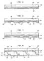
- FIG. 1is a front elevational view of a connector constructed in accordance with one embodiment of the present invention
- FIG. 2is a front elevational view of the connector shown in FIG. 1 in assembled relationship with a semiconductor chip using a layer of anisotropic conductive material;
- FIG. 3is a front elevational view of a connector constructed in accordance with another embodiment of the present invention.
- FIG. 4is a front elevational view of the connector shown in FIG. 3 in assembled relationship with a semiconductor chip using a layer of anisotropic conductive material;
- FIGS. 5-10are sequential front elevational views showing the steps in the process of making the connector shown in FIG. 3;
- FIG. 11is a front elevational view of a connector constructed in accordance with another embodiment of the present invention and in assembled relationship with a semiconductor chip using a layer of anisotropic conductive material;
- FIG. 12is a front elevational view of a connector constructed in accordance with one embodiment of the present invention in assembled relationship with first and second microelectronic elements using at least one layer of an anisotropic conductive material;
- FIG. 13is a front elevational view of a connector constructed in accordance with another embodiment of the present invention and in assembled relationship with first and second microelectronic elements using at least one layer of an anisotropic conductive material;
- FIG. 14is a front elevational view of a connector constructed in accordance with another embodiment of the present invention in assembled relationship with first and second microelectronic elements using at least one layer of an anisotropic conductive material;
- FIG. 15is a front elevational view of a connector constructed in accordance with another embodiment of the present invention in assembled relationship with first and second microelectronic elements using at least one layer of an anisotropic conductive material;
- FIG. 16is a front elevational view of a connector constructed in accordance with another embodiment of the present invention in assembled relationship with first and second microelectronic elements using at least one layer of an anisotropic conductive material;
- FIG. 17is a front elevational view of a connector constructed in accordance with another embodiment of the present invention in assembled relationship with first and second microelectronic elements using at least one layer of an anisotropic conductive material;
- FIG. 1a connector or connection component constructed in accordance with one embodiment of the present invention and generally designated by reference numeral 100 .
- the connector 100can be used to provide electrical connection between two microelectronic components, for example, a semiconductor chip, printed circuit board, circuit panel or other microelectronic device. Where the connector 100 is constructed from flexible or compliant materials, the connector can accommodate relative movement between the connected microelectronic components resulting from their thermal expansion and contraction.
- the connector 100is generally constructed from a body 102 of dielectric material having a generally planar first surface 104 and an opposing spaced apart generally planar second surface 106 .
- a plurality of electrically conductive elongated leadsextend through the body 102 between the first and second surfaces 104 , 106 .
- the leads 108are provided with first ends 110 generally accessible at the first surface 104 and second ends 112 generally accessible at the second surface 106 .
- the first and second ends of leads 108in accordance with one embodiment, are offset from each other in horizontal direction, as shown in FIG. 1, to form an S-shaped profile.
- the leadsmay have other shaped profiles such as straight where the first and second ends 110 , 112 are arranged generally overlying each other in collinear alignment such as disclosed in certain embodiments of the '964 Patent.
- the first and second ends 110 , 112 of the leads 108can be arranged in various patterns and matrices which may be the same or different as will be understood from the further description of the present invention.
- a microelectronic package 114formed by electrically connecting a connector 100 to a microelectronic element such as a semiconductor chip 116 .
- the semiconductor chip 116has an exposed face 118 which includes a plurality of contact terminals 120 arranged in a predetermined array.
- the second ends 112 of the leads 108are arranged in a corresponding array to the contact terminals 120 .
- the second ends 112form contacts for electrical connection to the contact terminals 120 of the semiconductor chip 116 .
- the connector 100is adhered to the semiconductor chip 116 to provide electrical continuity between the contact terminals 120 and leads 108 by a layer of anisotropic conductive material 122 which in accordance with the preferred embodiment has adhesive properties.
- the material 122 in describing the following examplewill therefore be designated for illustration purposes as adhesive 122 .
- the anisotropic conductive adhesivecan be provided in the form of a paste or a preformed sheet.
- the layer of anisotropic conductive adhesive 122may be deposited onto the first surface 104 of the body 102 or the exposed face 118 of the semiconductor chip 116 .
- anisotropic conductive adhesive 122is electrically conductive only in the vertical direction, i.e., between the contact terminals 120 and first ends 110 of the leads 108 , it is not required that the adhesive be stenciled in a pattern only over the contact terminals.
- the anisotropic conductive adhesive 122is generally applied over the entire first surface 104 of the connector 100 or the corresponding exposed face 118 of the semiconductor chip 116 .
- the microelectronic package 114can be electrically mounted to another microelectronic element such as a circuit panel by, for example, solder balls 124 which are attachable in electrical continuity to the second ends 112 of the leads 108 at the second surface 106 of the connector 100 or, for example, another layer of anisotropic conductive adhesive (not shown) at the second surface.
- solder balls 124which are attachable in electrical continuity to the second ends 112 of the leads 108 at the second surface 106 of the connector 100 or, for example, another layer of anisotropic conductive adhesive (not shown) at the second surface.
- the connector 100is adhered to a semiconductor chip 116 by the adhesive properties of the anisotropic conductive material 122 in accordance with the preferred embodiment.
- the anisotropic conductive material 122can be provided with an adhesive layer, such as a non-conductive adhesive, as well as at other locations which do not interfere with the conductive path between the ends of the leads 108 and contact terminals 120 on the semiconductor chip 116 .
- other techniquescan be used, for example, mechanical clamping, encapsulation of the connector 100 and semiconductor chip 116 , and the like.
- FIGS. 3 and 4there is disclosed another embodiment of a connector 100 and microelectronic package 114 in accordance with the preferred embodiment of the present invention.
- the connector 100is formed with a plurality of individual electrically conductive contacts 126 .
- the contacts 126are formed in the first surface 104 of the body 102 in alignment with the first ends 110 of the leads 108 .
- the first ends 110 of the leads 108are attached to the contacts 126 to provide electrical continuity.
- the connectors shown in FIGS. 1 and 3are generally of similar construction.
- the contacts 126are electrically connected to the contact terminals 120 of the semiconductor chip 116 using the anisotropic conductive adhesive 122 as thus far described with respect to the microelectronic package 114 in FIG. 2 . It can therefore be appreciated that connectors 100 and microelectronic packages 114 can be constructed either with or without separate contacts 126 .
- a planar substrate 128 which functions as a mandrillis provided with a generally planar surface 130 .
- the substrate 128can be formed from a variety of rigid materials such as borosilicate glass, aluminum and the like.
- a layer of releasable adhesive 132such as, for example a heat or UV releasable adhesive, is applied over the surface 130 of the substrate 128 .
- a sacrificial sheet of an electrically conductive material 134such as aluminum foil, is laminated onto the adhesive layer 132 .
- sacrificial layer 134such as chrome, nickel, alloys or combinations thereof, or other electrically conductive metals which are capable of being selectively etched with respect to the metal of the copper layer 136 , can be provided on the adhesive layer 132 .
- a copper layer 136is formed on the aluminum layer 134 .
- the copper layer 136may be formed by known processes such as lamination, sputtering or electroless plating followed by electroplating.
- the exposed copper layer 136is circuitized to form the desired features of the connector 100 such as leads 108 , circuit traces, bonding pads, solder ball pads and the like.
- the first ends 110 of the leads 108can function as bonding pads while the second ends 112 of the leads can function as solder ball pads.
- the first ends 110 of the leads 108can be arranged in an array corresponding to the array of the contact terminals 120 on the semiconductor chip 116 .
- the first ends 110can be arranged in an area array, i.e., an array of features arranged in a substantially regular pattern with a substantially uniform density of features throughout the horizontal extent of the pattern.
- the second ends 112 of the leads 108can be arranged in an array corresponding to the array of the contact terminals of the microelectronic element to which the second ends are to be electrically attached via the solder balls 124 .
- the leads 108as well as the other circuit features can be formed from the copper layer 136 , by way of one example only, by conventional photographic processes. It is to be understood that the leads 108 may be fabricated from essentially any conductive material, but most typically being formed from conductive metals such as copper, copper alloys, gold, gold alloys and composites including layers of these metals.
- the leads 108are made peelable from the aluminum layer 134 using any one of a number of conventional processes as to be described hereinafter.
- a fusible metal such as a tin/lead alloyis selectively plated onto the first ends 110 of the leads 108 to form a plurality of conductive contacts 138 .
- the contacts 138may be overplated with a non-oxidizable metal layer, for example, gold.
- the contacts 138are bonded to a temporary support 140 such as a sheet of solder-wettable metal such as copper, copper alloys and the like.
- the resulting structure, as shown in FIG. 7,is subject to vertical expansion through, for example, separation of vacuum platens or pressurized injection of an elastomeric encapsulant.
- the temporary support 140 and the substrate 128are moved vertically away from one another through a predetermined displacement, and horizontally relative to one another, so that the first end 112 of the lead 108 moves horizontally toward and vertically away from the first end 110 of the lead.
- the temporary support 140may be engaged with a lower platen while the substrate 128 may be engaged with an upper platen.
- the engagementmay be maintained by applying a vacuum through each of the platens to hold the substrate 128 and temporary support 140 firmly in engagement with the platens as the platens are moved away from one another.
- the relative movement of the lead ends 110 , 112bend the main portion of the lead 108 .
- a flowable materialsuch as a liquid composition 142 capable of curing to form a compliant dielectric material such as a gel or an elastomer is injected between the temporary support 140 and aluminum layer 134 .
- the curable liquid composition 142may be a silicone or epoxy composition which forms a compliant flexible body.
- the curable liquid composition 142may be in the nature of a rigid polymer material if desired. If the liquid composition 142 is injected during the movement step, the pressure of the flowable composition will help to force the temporary support 140 and substrate 128 away from each other, either with or without assistance from the platens.
- the liquid composition 142is then cured to form a compliant dielectric layer having a first surface 144 formed in contact with the temporary support 140 and a second surface 146 formed in contact with the sacrificial aluminum layer 134 .
- the temporary support 140is removed by, for example, reflowing the fusible metal forming the contacts 138 .
- the temporary support 140may be removed by other techniques such as ablation, plasma or wet chemical etching. However, the latter methods will require that the temporary support 140 be constructed of a material whose etchant will not attack the remaining structure of the connector 100 , such as the contacts 138 , leads 108 , etc.
- the resulting structure as shown in FIG. 9is further released from the temporary support 128 by heating or application of UV radiation to release the adhesive layer 132 .
- the sacrificial aluminum layer 134is etched away using a suitable etchant, leaving the second ends 112 forming solder ball pads 148 exposed on the second surface 106 .
- Conductive metalsuch as copper, copper gold alloy and the like may be plated onto the exposed surface of the solder ball pads 148 if desired to enhance bonding of the solder balls 124 .
- Residual fusible material on the contacts 138can be etched away when etching the aluminum sacrificial layer 134 using a suitable etchant such as hydrochloric acid.
- the resulting connector 100is illustrated in FIG. 3 as previously described. It is to be understood that the contacts 138 are not an essential component of the connector 100 .
- the contacts 138may be omitted during the manufacturing process to produce the connector 100 as shown in FIG. 1 .
- the first ends 110 of the leads 108 adjacent the first surface 104 of the body 102will function as contacts for joining with the contact terminals 120 of the semiconductor chip 116 .
- the first ends 110 of the leads 108can be joined to the temporary support 140 by stenciling fusible material thereon, and later removing same by chemical etching.
- the anisotropic conductive adhesive 122is provided as a continuous preformed sheet or layer in the form of a paste which is provided over substantially all of the contacts 126 , 138 and exposed first surface of the body 102 .
- the anisotropic conductive adhesive 122can alternatively be applied over exposed face 118 of the semiconductor chip 116 .
- the anisotropic conductive adhesive 122is preferably a polymeric resin having a matrix of conductive particles therein, such as the conductive particles as shown in FIG. 2 .
- the anisotropic conductive adhesive 122need not be flexible and/or compliant such as preferred with respect to the composition 142 forming the body 102 . In this regard, the anisotropic conductive adhesive 122 may be formed in the nature of a rigid layer.
- the anisotropic conductive adhesive 122becomes conductive in the pressed direction due to the continuity of the conductive material, for example, the metallic powders, caused by the pressure.
- the conductive particlesmay include metallic powders such as nickel or gold.
- the metallic powdersmay also be, for example, metallic particles consisting of resin particles coated with Ni-plated layers or the like, or solid metallic particles consisting of gold, nickel or the like.
- the particlesmay, for example, be in the size range of from about 3 to 15 microns, preferably as solid balls of nickel or gold.
- One suitable anisotropic conductive materialincludes the material sold under the tradename “FC-262B” by the Hitachi Chemical Company. The exact composition and characteristics of the FC-262B anisotropic conductive material are set forth in more detail in the chemical data sheet for the FC-262B material, which is incorporated herein by reference.
- an anisotropic conductive adhesive 122for electrically connecting the flexible leads 108 and chip contacts 120 .
- metal-to-metal (“intermetallic”) bondingrequiring the use of high temperatures/pressures during thermocompression or thermosonic bonding.
- an anisotropic conductive adhesive 122when using an anisotropic conductive adhesive 122 to attach the leads 108 to the contacts 120 , lower temperatures and pressures will be required to make the connections. The lower temperatures and pressures will minimize stresses on the connector 100 which, in turn, will minimize the potential for the fatigue related problems.
- Another benefit of bonding at lower temperatures and pressuresis that finer flexible leads 108 may be used which will enable even finer pitches to be obtained (i.e., more leads in the same space).
- the connector 160includes a layer 162 generally in the nature of a single layer of dielectric material such as a polyimide.
- the layer 162is illustrated as including only a single layer of dielectric material, it should be appreciated that it can include other features such as multiple dielectric layers, electrically conductive traces extending in horizontal directions along the surfaces of the body or within the body, electrically conductive ground planes or power planes also extending in a horizontal direction on a surface of the body within the body, as well as electrically conductive vias connecting these features with one another.
- a plurality of vias 164lined with an electrically conductive material, such as copper, extend through the layer 162 into electrical connection with the leads 108 .
- first and second ends 110 , 112 of the leads 108can be redistributed on the first and second surfaces 104 , 106 of the connector 100 , 160 . Redistribution can be achieved, by way of example, using conductive traces which extend to the desired location for redistributing the pattern or matrix of the first and second ends of the leads 108 .
- the conductive traces(not shown) can be preformed on the dielectric body 102 using conventional techniques, for example, a patterned photomask followed by conductive metal deposition, e.g., sputtering, followed by electroless and/or electroplating.
- the solder balls 124 as shown in FIG. 11can be at any location desired so as to mate with conductive terminals on a microelectronic element such as a printed circuit board or other semiconductor chip and the like.
- the conductive tracescan be electrically connected to the vias.
- the connector 160can be made in accordance with the methods as thus far described, wherein the dielectric layer 162 is used in place of the sacrificial aluminum layer 134 .
- the dielectric layer 162may be applied to the second surface 106 of the body 102 after manufacture, as well as being an integral part of the manufacturing processes as disclosed in the '694 Patent, the disclosure of which is incorporated herein by reference.
- the leads 108are made peelable from the sacrificial aluminum layer 134 or dielectric layer 162 using a variety of techniques.
- the sacrificial aluminum layer 134can be subjected to a selective etchant process by exposing portions of the aluminum layer to a liquid etch solution which attacks the layer so as to undercut the leads 108 and remove the sacrificial aluminum layer from beneath the etch resistant leads at all locations except at their second ends 112 . At the second ends 112 , most, but not all of the sacrificial aluminum layer is removed.
- This method of forming peelable leadsis further disclosed in the '964 Patent which is incorporated herein by reference.
- microelectronic package 170is provided with a pair of microelectronic elements 172 , 174 .
- the microelectronic elements 172 , 174may include, for example, semiconductor chips, printed circuit boards, circuit panels, other microelectronic devices and the like.
- the microelectronic element 172is electrically connected to the leads 108 using a layer of conductive anisotropic material 122 preferably having adhesive properties.
- the face of the microelectronic element 172can be provided with a plurality of contact terminals (not shown) arranged in the appropriate matrix or array.
- a second microelectronic element 174is similarly electrically mounted for electrical connection to the leads 108 on the other surface of the connector 100 using a layer of anisotropic conductive material 122 .
- Solder balls 124may be provided in contact with the ends of the leads 108 which are exposed on either side of the microelectronic element 174 . It is preferred that the height of the solder balls 124 be larger than the combined height of the anisotropic conductive material 122 and microelectronic element 174 . This enables the microelectronic package 170 to be bonded to another microelectronic element such as a printed circuit board via the solder balls 124 .
- microelectronic package 176constructed in accordance with another embodiment of the present invention.
- the ends of the leads 108are redistributed to allow the microelectronic element 174 to be wire bonded via the conductive wires 178 .
- the microelectronic element 174 and surrounding bond wires 178are encapsulated by, for example, overmolding with a polymer material, which may be rigid or flexible.
- the encapsulantis a dielectric material.
- FIG. 14there is disclosed another embodiment of a microelectronic package 182 .
- the microelectronic element 172is in the nature of a bump chip having a plurality of contact terminals 184 .
- the contact terminals 184are in electrical continuity with the free ends of the leads 108 via the anisotropic conductive material 122 .
- the microelectronic element 174 via the anisotropic conductive material 122is in electrical continuity with redistributed leads on the surface of a flexible polyimide layer 185 .
- the polyimide layer 185is provided with a plurality of plated through vias 164 for electrical connection to the ends of the leads 108 .
- the solder balls 124are in direct electrical connection to the vias 164 which provide continuity to the ends of the leads 104 .
- FIG. 15there is shown another embodiment of a microelectronic package 186 .
- the package 186is provided with a dielectric polyimide layer 185 which is rigid and extends beyond the periphery of the connector 100 , and may include a plurality of plated through vias 164 .
- the resulting packageis encapsulated with an encapsulant 188 similar to the encapsulant 180 as previously described.
- the larger dielectric layer 185allows for the arrangement of a greater number of solder balls 124 for interconnection to another microelectronic element.
- FIG. 16there is shown a microelectronic package 190 constructed in accordance with another embodiment of the present invention.
- the microelectronic element 174is connected to the connector 100 via a second connector 192 comprising a plurality of leads 194 embedded in a compliant layer 196 .
- the leads 194may be in alignment with for direct electrical connection to the ends of the leads 108 as shown in the left hand portion of the connector 192 .
- the ends of the leads 108may be redistributed for connection to the ends of the leads 194 as shown in the right hand portion of the connector 192 .
- the second connector 192can be constructed in a similar manner as connector 100 . However, it is to be understood that other methods of forming the connector 192 can be used.
- a layer of anisotropic conductive materialmay be sandwiched between the first and second connectors 100 , 192 .
- FIG. 17there is shown a microelectronic package 196 constructed in accordance with another embodiment of the present invention.
- the microelectronic element 174is in the nature of a bump chip or flip chip having a plurality of conductive bumps 198 thereon.
- the ends of the leads 108 on the surface of the connector 100may be redistributed if necessary into an array corresponding to an array of the bumps 198
Landscapes
- Engineering & Computer Science (AREA)
- Physics & Mathematics (AREA)
- Condensed Matter Physics & Semiconductors (AREA)
- General Physics & Mathematics (AREA)
- Computer Hardware Design (AREA)
- Microelectronics & Electronic Packaging (AREA)
- Power Engineering (AREA)
- Manufacturing & Machinery (AREA)
- Wire Bonding (AREA)
Abstract
Description
Claims (51)
Priority Applications (2)
| Application Number | Priority Date | Filing Date | Title |
|---|---|---|---|
| US10/139,169US6825552B2 (en) | 2001-05-09 | 2002-05-06 | Connection components with anisotropic conductive material interconnection |
| US10/994,695US20050064626A1 (en) | 2001-05-09 | 2004-11-22 | Connection components with anistropic conductive material interconnector |
Applications Claiming Priority (2)
| Application Number | Priority Date | Filing Date | Title |
|---|---|---|---|
| US28971801P | 2001-05-09 | 2001-05-09 | |
| US10/139,169US6825552B2 (en) | 2001-05-09 | 2002-05-06 | Connection components with anisotropic conductive material interconnection |
Related Child Applications (1)
| Application Number | Title | Priority Date | Filing Date |
|---|---|---|---|
| US10/994,695DivisionUS20050064626A1 (en) | 2001-05-09 | 2004-11-22 | Connection components with anistropic conductive material interconnector |
Publications (2)
| Publication Number | Publication Date |
|---|---|
| US20030068906A1 US20030068906A1 (en) | 2003-04-10 |
| US6825552B2true US6825552B2 (en) | 2004-11-30 |
Family
ID=26836939
Family Applications (2)
| Application Number | Title | Priority Date | Filing Date |
|---|---|---|---|
| US10/139,169Expired - LifetimeUS6825552B2 (en) | 2001-05-09 | 2002-05-06 | Connection components with anisotropic conductive material interconnection |
| US10/994,695AbandonedUS20050064626A1 (en) | 2001-05-09 | 2004-11-22 | Connection components with anistropic conductive material interconnector |
Family Applications After (1)
| Application Number | Title | Priority Date | Filing Date |
|---|---|---|---|
| US10/994,695AbandonedUS20050064626A1 (en) | 2001-05-09 | 2004-11-22 | Connection components with anistropic conductive material interconnector |
Country Status (1)
| Country | Link |
|---|---|
| US (2) | US6825552B2 (en) |
Cited By (31)
| Publication number | Priority date | Publication date | Assignee | Title |
|---|---|---|---|---|
| US20050023682A1 (en)* | 2003-07-31 | 2005-02-03 | Morio Nakao | High reliability chip scale package |
| US7098073B1 (en) | 2005-04-18 | 2006-08-29 | Freescale Semiconductor, Inc. | Method for stacking an integrated circuit on another integrated circuit |
| US20060231938A1 (en)* | 2005-04-18 | 2006-10-19 | Mangrum Marc A | Structure for stacking an integrated circuit on another integrated circuit |
| US20070014095A1 (en)* | 2005-07-12 | 2007-01-18 | Weiss Roger E | High-performance separable electrical device/printed circuit board interconnection |
| US20070158816A1 (en)* | 2006-01-12 | 2007-07-12 | Palo Alto Research Center Incorporated | Contact spring application to semiconductor devices |
| WO2008060772A1 (en)* | 2006-11-17 | 2008-05-22 | Freescale Semiconductor Inc. | Method of packaging a device having a multi-contact elastomer connector contact area and device thereof |
| US20080116560A1 (en)* | 2006-11-17 | 2008-05-22 | Mangrum Marc A | Method of packaging a device having a tangible element and device thereof |
| US20080119013A1 (en)* | 2006-11-17 | 2008-05-22 | Mangrum Marc A | Method of packaging a device using a dielectric layer |
| US20090286390A1 (en)* | 2006-11-17 | 2009-11-19 | Freescale Semiconductor, Inc. | Method of packaging a semiconductor device and a prefabricated connector |
| US8518304B1 (en) | 2003-03-31 | 2013-08-27 | The Research Foundation Of State University Of New York | Nano-structure enhancements for anisotropic conductive material and thermal interposers |
| US20160163639A1 (en)* | 2012-05-22 | 2016-06-09 | Invensas Corporation | Substrate-less Stackable Package with Wire-Bond Interconnect |
| US9728527B2 (en) | 2013-11-22 | 2017-08-08 | Invensas Corporation | Multiple bond via arrays of different wire heights on a same substrate |
| US9735084B2 (en) | 2014-12-11 | 2017-08-15 | Invensas Corporation | Bond via array for thermal conductivity |
| US9761554B2 (en) | 2015-05-07 | 2017-09-12 | Invensas Corporation | Ball bonding metal wire bond wires to metal pads |
| US9812402B2 (en) | 2015-10-12 | 2017-11-07 | Invensas Corporation | Wire bond wires for interference shielding |
| US9842745B2 (en) | 2012-02-17 | 2017-12-12 | Invensas Corporation | Heat spreading substrate with embedded interconnects |
| US9852969B2 (en) | 2013-11-22 | 2017-12-26 | Invensas Corporation | Die stacks with one or more bond via arrays of wire bond wires and with one or more arrays of bump interconnects |
| US9888579B2 (en) | 2015-03-05 | 2018-02-06 | Invensas Corporation | Pressing of wire bond wire tips to provide bent-over tips |
| US9911718B2 (en) | 2015-11-17 | 2018-03-06 | Invensas Corporation | ‘RDL-First’ packaged microelectronic device for a package-on-package device |
| US9935075B2 (en) | 2016-07-29 | 2018-04-03 | Invensas Corporation | Wire bonding method and apparatus for electromagnetic interference shielding |
| US9984992B2 (en) | 2015-12-30 | 2018-05-29 | Invensas Corporation | Embedded wire bond wires for vertical integration with separate surface mount and wire bond mounting surfaces |
| US10008469B2 (en) | 2015-04-30 | 2018-06-26 | Invensas Corporation | Wafer-level packaging using wire bond wires in place of a redistribution layer |
| US10026717B2 (en) | 2013-11-22 | 2018-07-17 | Invensas Corporation | Multiple bond via arrays of different wire heights on a same substrate |
| US10062661B2 (en) | 2011-05-03 | 2018-08-28 | Tessera, Inc. | Package-on-package assembly with wire bonds to encapsulation surface |
| US10181457B2 (en) | 2015-10-26 | 2019-01-15 | Invensas Corporation | Microelectronic package for wafer-level chip scale packaging with fan-out |
| US10299368B2 (en) | 2016-12-21 | 2019-05-21 | Invensas Corporation | Surface integrated waveguides and circuit structures therefor |
| US10381326B2 (en) | 2014-05-28 | 2019-08-13 | Invensas Corporation | Structure and method for integrated circuits packaging with increased density |
| US10490528B2 (en) | 2015-10-12 | 2019-11-26 | Invensas Corporation | Embedded wire bond wires |
| US11189595B2 (en) | 2011-10-17 | 2021-11-30 | Invensas Corporation | Package-on-package assembly with wire bond vias |
| US11404338B2 (en) | 2014-01-17 | 2022-08-02 | Invensas Corporation | Fine pitch bva using reconstituted wafer with area array accessible for testing |
| US20240040808A1 (en)* | 2020-09-03 | 2024-02-01 | Applied Materials, Inc. | Techniques and device structure based upon directional seeding and selective deposition |
Families Citing this family (19)
| Publication number | Priority date | Publication date | Assignee | Title |
|---|---|---|---|---|
| US7750487B2 (en)* | 2004-08-11 | 2010-07-06 | Intel Corporation | Metal-metal bonding of compliant interconnect |
| NL1027450C2 (en)* | 2004-11-09 | 2006-05-10 | Shin Etsu Polymer Europ B V | Interconnection connector, frame comprising such a connector, electrical measuring and testing device and contacting method with the aid of such a connector. |
| ATE418764T1 (en)* | 2005-03-30 | 2009-01-15 | Nxp Bv | CONNECTABLE HOUSING FOR A PORTABLE OBJECT |
| JP4432949B2 (en)* | 2006-09-15 | 2010-03-17 | パナソニック株式会社 | Electrical component connection method |
| US8493749B2 (en)* | 2009-10-12 | 2013-07-23 | Apple Inc. | Conforming EMI shielding |
| US8278748B2 (en) | 2010-02-17 | 2012-10-02 | Maxim Integrated Products, Inc. | Wafer-level packaged device having self-assembled resilient leads |
| US8482111B2 (en) | 2010-07-19 | 2013-07-09 | Tessera, Inc. | Stackable molded microelectronic packages |
| US8372741B1 (en) | 2012-02-24 | 2013-02-12 | Invensas Corporation | Method for package-on-package assembly with wire bonds to encapsulation surface |
| US9391008B2 (en) | 2012-07-31 | 2016-07-12 | Invensas Corporation | Reconstituted wafer-level package DRAM |
| US9502390B2 (en) | 2012-08-03 | 2016-11-22 | Invensas Corporation | BVA interposer |
| TWM458697U (en)* | 2012-09-17 | 2013-08-01 | Hon Hai Prec Ind Co Ltd | Contact and connector assembled with said contact |
| US8878353B2 (en) | 2012-12-20 | 2014-11-04 | Invensas Corporation | Structure for microelectronic packaging with bond elements to encapsulation surface |
| US9167710B2 (en) | 2013-08-07 | 2015-10-20 | Invensas Corporation | Embedded packaging with preformed vias |
| US9685365B2 (en) | 2013-08-08 | 2017-06-20 | Invensas Corporation | Method of forming a wire bond having a free end |
| US20150076714A1 (en) | 2013-09-16 | 2015-03-19 | Invensas Corporation | Microelectronic element with bond elements to encapsulation surface |
| US9455228B2 (en) | 2014-01-03 | 2016-09-27 | Apple Inc. | Self-shielded components and methods for making the same |
| US10332854B2 (en) | 2015-10-23 | 2019-06-25 | Invensas Corporation | Anchoring structure of fine pitch bva |
| US9659848B1 (en) | 2015-11-18 | 2017-05-23 | Invensas Corporation | Stiffened wires for offset BVA |
| JP6733493B2 (en)* | 2016-10-25 | 2020-07-29 | 株式会社オートネットワーク技術研究所 | Electrical contacts, connector terminal pairs, and connector pairs |
Citations (35)
| Publication number | Priority date | Publication date | Assignee | Title |
|---|---|---|---|---|
| US4729809A (en) | 1985-03-14 | 1988-03-08 | Amp Incorporated | Anisotropically conductive adhesive composition |
| US4811081A (en) | 1987-03-23 | 1989-03-07 | Motorola, Inc. | Semiconductor die bonding with conductive adhesive |
| US4955132A (en) | 1987-11-16 | 1990-09-11 | Sharp Kabushiki Kaisha | Method for mounting a semiconductor chip |
| US5001542A (en) | 1988-12-05 | 1991-03-19 | Hitachi Chemical Company | Composition for circuit connection, method for connection using the same, and connected structure of semiconductor chips |
| US5128831A (en) | 1991-10-31 | 1992-07-07 | Micron Technology, Inc. | High-density electronic package comprising stacked sub-modules which are electrically interconnected by solder-filled vias |
| US5148265A (en) | 1990-09-24 | 1992-09-15 | Ist Associates, Inc. | Semiconductor chip assemblies with fan-in leads |
| US5148266A (en) | 1990-09-24 | 1992-09-15 | Ist Associates, Inc. | Semiconductor chip assemblies having interposer and flexible lead |
| US5161090A (en) | 1991-12-13 | 1992-11-03 | Hewlett-Packard Company | Heat pipe-electrical interconnect integration for chip modules |
| US5216278A (en) | 1990-12-04 | 1993-06-01 | Motorola, Inc. | Semiconductor device having a pad array carrier package |
| US5225966A (en) | 1991-07-24 | 1993-07-06 | At&T Bell Laboratories | Conductive adhesive film techniques |
| US5360992A (en) | 1991-12-20 | 1994-11-01 | Micron Technology, Inc. | Two piece assembly for the selection of pinouts and bond options on a semiconductor device |
| US5428190A (en) | 1993-07-02 | 1995-06-27 | Sheldahl, Inc. | Rigid-flex board with anisotropic interconnect and method of manufacture |
| US5431571A (en) | 1993-11-22 | 1995-07-11 | W. L. Gore & Associates, Inc. | Electrical conductive polymer matrix |
| US5457149A (en) | 1990-06-08 | 1995-10-10 | Minnesota Mining And Manufacturing Company | Reworkable adhesive for electronic applications |
| US5518964A (en) | 1994-07-07 | 1996-05-21 | Tessera, Inc. | Microelectronic mounting with multiple lead deformation and bonding |
| US5627405A (en) | 1995-07-17 | 1997-05-06 | National Semiconductor Corporation | Integrated circuit assembly incorporating an anisotropic elecctrically conductive layer |
| US5631191A (en) | 1993-08-27 | 1997-05-20 | Poly-Flex Circuits, Inc. | Method for connecting a die to electrically conductive traces on a flexible lead-frame |
| US5657206A (en) | 1994-06-23 | 1997-08-12 | Cubic Memory, Inc. | Conductive epoxy flip-chip package and method |
| US5677576A (en) | 1995-03-24 | 1997-10-14 | Shinko Electric Industries Co., Ltd. | Chip sized semiconductor device |
| US5679977A (en) | 1990-09-24 | 1997-10-21 | Tessera, Inc. | Semiconductor chip assemblies, methods of making same and components for same |
| US5749997A (en) | 1995-12-27 | 1998-05-12 | Industrial Technology Research Institute | Composite bump tape automated bonding method and bonded structure |
| US5848468A (en) | 1994-10-04 | 1998-12-15 | Hagen Batterie Ag | Method of forming metallic current conducting lugs at electrode plates of accumulators |
| US5852326A (en) | 1990-09-24 | 1998-12-22 | Tessera, Inc. | Face-up semiconductor chip assembly |
| US5861678A (en) | 1997-12-23 | 1999-01-19 | Micron Technology, Inc. | Method and system for attaching semiconductor dice to substrates |
| US5904498A (en) | 1995-10-24 | 1999-05-18 | Tessera, Inc. | Connection component with releasable leads |
| US5933712A (en) | 1997-03-19 | 1999-08-03 | The Regents Of The University Of California | Attachment method for stacked integrated circuit (IC) chips |
| US5989936A (en) | 1994-07-07 | 1999-11-23 | Tessera, Inc. | Microelectronic assembly fabrication with terminal formation from a conductive layer |
| US6008072A (en) | 1995-12-27 | 1999-12-28 | Industrial Technology Research Institute | Tape automated bonding method |
| US6028354A (en) | 1997-10-14 | 2000-02-22 | Amkor Technology, Inc. | Microelectronic device package having a heat sink structure for increasing the thermal conductivity of the package |
| US6093970A (en) | 1994-11-22 | 2000-07-25 | Sony Corporation | Semiconductor device and method for manufacturing the same |
| US6117694A (en) | 1994-07-07 | 2000-09-12 | Tessera, Inc. | Flexible lead structures and methods of making same |
| US6150194A (en) | 1996-12-04 | 2000-11-21 | Shinko Electric Industries Co., Ltd. | Semiconductor device sealed with resin, and its manufacture |
| US6265765B1 (en)* | 1994-07-07 | 2001-07-24 | Tessera, Inc. | Fan-out semiconductor chip assembly |
| US6333207B1 (en)* | 1999-05-24 | 2001-12-25 | Tessera, Inc. | Peelable lead structure and method of manufacture |
| US6468830B1 (en)* | 1998-01-26 | 2002-10-22 | Tessera, Inc. | Compliant semiconductor package with anisotropic conductive material interconnects and methods therefor |
Family Cites Families (1)
| Publication number | Priority date | Publication date | Assignee | Title |
|---|---|---|---|---|
| US5148286A (en)* | 1990-09-28 | 1992-09-15 | Xerox Corporation | Method and apparatus for operating an electronic reprographic printing system upon scan interruption |
- 2002
- 2002-05-06USUS10/139,169patent/US6825552B2/ennot_activeExpired - Lifetime
- 2004
- 2004-11-22USUS10/994,695patent/US20050064626A1/ennot_activeAbandoned
Patent Citations (42)
| Publication number | Priority date | Publication date | Assignee | Title |
|---|---|---|---|---|
| US4729809A (en) | 1985-03-14 | 1988-03-08 | Amp Incorporated | Anisotropically conductive adhesive composition |
| US4811081A (en) | 1987-03-23 | 1989-03-07 | Motorola, Inc. | Semiconductor die bonding with conductive adhesive |
| US4955132A (en) | 1987-11-16 | 1990-09-11 | Sharp Kabushiki Kaisha | Method for mounting a semiconductor chip |
| US5001542A (en) | 1988-12-05 | 1991-03-19 | Hitachi Chemical Company | Composition for circuit connection, method for connection using the same, and connected structure of semiconductor chips |
| US5457149A (en) | 1990-06-08 | 1995-10-10 | Minnesota Mining And Manufacturing Company | Reworkable adhesive for electronic applications |
| US5679977A (en) | 1990-09-24 | 1997-10-21 | Tessera, Inc. | Semiconductor chip assemblies, methods of making same and components for same |
| US5148265A (en) | 1990-09-24 | 1992-09-15 | Ist Associates, Inc. | Semiconductor chip assemblies with fan-in leads |
| US5685885A (en) | 1990-09-24 | 1997-11-11 | Tessera, Inc. | Wafer-scale techniques for fabrication of semiconductor chip assemblies |
| US5148266A (en) | 1990-09-24 | 1992-09-15 | Ist Associates, Inc. | Semiconductor chip assemblies having interposer and flexible lead |
| US6372527B1 (en) | 1990-09-24 | 2002-04-16 | Tessera, Inc. | Methods of making semiconductor chip assemblies |
| US5347159A (en) | 1990-09-24 | 1994-09-13 | Tessera, Inc. | Semiconductor chip assemblies with face-up mounting and rear-surface connection to substrate |
| US6392306B1 (en) | 1990-09-24 | 2002-05-21 | Tessera, Inc. | Semiconductor chip assembly with anisotropic conductive adhesive connections |
| US5852326A (en) | 1990-09-24 | 1998-12-22 | Tessera, Inc. | Face-up semiconductor chip assembly |
| US5216278A (en) | 1990-12-04 | 1993-06-01 | Motorola, Inc. | Semiconductor device having a pad array carrier package |
| US5225966A (en) | 1991-07-24 | 1993-07-06 | At&T Bell Laboratories | Conductive adhesive film techniques |
| US5128831A (en) | 1991-10-31 | 1992-07-07 | Micron Technology, Inc. | High-density electronic package comprising stacked sub-modules which are electrically interconnected by solder-filled vias |
| US5161090A (en) | 1991-12-13 | 1992-11-03 | Hewlett-Packard Company | Heat pipe-electrical interconnect integration for chip modules |
| US5360992A (en) | 1991-12-20 | 1994-11-01 | Micron Technology, Inc. | Two piece assembly for the selection of pinouts and bond options on a semiconductor device |
| US5428190A (en) | 1993-07-02 | 1995-06-27 | Sheldahl, Inc. | Rigid-flex board with anisotropic interconnect and method of manufacture |
| US5631191A (en) | 1993-08-27 | 1997-05-20 | Poly-Flex Circuits, Inc. | Method for connecting a die to electrically conductive traces on a flexible lead-frame |
| US5431571A (en) | 1993-11-22 | 1995-07-11 | W. L. Gore & Associates, Inc. | Electrical conductive polymer matrix |
| US5657206A (en) | 1994-06-23 | 1997-08-12 | Cubic Memory, Inc. | Conductive epoxy flip-chip package and method |
| US6104087A (en)* | 1994-07-07 | 2000-08-15 | Tessera, Inc. | Microelectronic assemblies with multiple leads |
| US5989936A (en) | 1994-07-07 | 1999-11-23 | Tessera, Inc. | Microelectronic assembly fabrication with terminal formation from a conductive layer |
| US5801441A (en)* | 1994-07-07 | 1998-09-01 | Tessera, Inc. | Microelectronic mounting with multiple lead deformation and bonding |
| US6117694A (en) | 1994-07-07 | 2000-09-12 | Tessera, Inc. | Flexible lead structures and methods of making same |
| US5518964A (en) | 1994-07-07 | 1996-05-21 | Tessera, Inc. | Microelectronic mounting with multiple lead deformation and bonding |
| US6307260B1 (en)* | 1994-07-07 | 2001-10-23 | Tessera, Inc. | Microelectronic assembly fabrication with terminal formation from a conductive layer |
| US6265765B1 (en)* | 1994-07-07 | 2001-07-24 | Tessera, Inc. | Fan-out semiconductor chip assembly |
| US5848468A (en) | 1994-10-04 | 1998-12-15 | Hagen Batterie Ag | Method of forming metallic current conducting lugs at electrode plates of accumulators |
| US6093970A (en) | 1994-11-22 | 2000-07-25 | Sony Corporation | Semiconductor device and method for manufacturing the same |
| US5677576A (en) | 1995-03-24 | 1997-10-14 | Shinko Electric Industries Co., Ltd. | Chip sized semiconductor device |
| US5627405A (en) | 1995-07-17 | 1997-05-06 | National Semiconductor Corporation | Integrated circuit assembly incorporating an anisotropic elecctrically conductive layer |
| US5904498A (en) | 1995-10-24 | 1999-05-18 | Tessera, Inc. | Connection component with releasable leads |
| US6008072A (en) | 1995-12-27 | 1999-12-28 | Industrial Technology Research Institute | Tape automated bonding method |
| US5749997A (en) | 1995-12-27 | 1998-05-12 | Industrial Technology Research Institute | Composite bump tape automated bonding method and bonded structure |
| US6150194A (en) | 1996-12-04 | 2000-11-21 | Shinko Electric Industries Co., Ltd. | Semiconductor device sealed with resin, and its manufacture |
| US5933712A (en) | 1997-03-19 | 1999-08-03 | The Regents Of The University Of California | Attachment method for stacked integrated circuit (IC) chips |
| US6028354A (en) | 1997-10-14 | 2000-02-22 | Amkor Technology, Inc. | Microelectronic device package having a heat sink structure for increasing the thermal conductivity of the package |
| US5861678A (en) | 1997-12-23 | 1999-01-19 | Micron Technology, Inc. | Method and system for attaching semiconductor dice to substrates |
| US6468830B1 (en)* | 1998-01-26 | 2002-10-22 | Tessera, Inc. | Compliant semiconductor package with anisotropic conductive material interconnects and methods therefor |
| US6333207B1 (en)* | 1999-05-24 | 2001-12-25 | Tessera, Inc. | Peelable lead structure and method of manufacture |
Non-Patent Citations (2)
| Title |
|---|
| Microelectronics Packaging Handbook, Subsystem Packaging, Part III, 2nd Edition, Rao R. Tummala, Eugene J. Rymaszewski, Alan G. Klopfenstein, Oct. 16, 1997. |
| Office Action mailed Oct. 21, 2003 relating to application Ser. No. 10/205,635. |
Cited By (55)
| Publication number | Priority date | Publication date | Assignee | Title |
|---|---|---|---|---|
| US8518304B1 (en) | 2003-03-31 | 2013-08-27 | The Research Foundation Of State University Of New York | Nano-structure enhancements for anisotropic conductive material and thermal interposers |
| US20050023682A1 (en)* | 2003-07-31 | 2005-02-03 | Morio Nakao | High reliability chip scale package |
| US7098073B1 (en) | 2005-04-18 | 2006-08-29 | Freescale Semiconductor, Inc. | Method for stacking an integrated circuit on another integrated circuit |
| US20060231938A1 (en)* | 2005-04-18 | 2006-10-19 | Mangrum Marc A | Structure for stacking an integrated circuit on another integrated circuit |
| US7196427B2 (en) | 2005-04-18 | 2007-03-27 | Freescale Semiconductor, Inc. | Structure having an integrated circuit on another integrated circuit with an intervening bent adhesive element |
| US20070014095A1 (en)* | 2005-07-12 | 2007-01-18 | Weiss Roger E | High-performance separable electrical device/printed circuit board interconnection |
| US7982290B2 (en)* | 2006-01-12 | 2011-07-19 | Palo Alto Research Center, Inc. | Contact spring application to semiconductor devices |
| US20070158816A1 (en)* | 2006-01-12 | 2007-07-12 | Palo Alto Research Center Incorporated | Contact spring application to semiconductor devices |
| US8318542B2 (en) | 2006-01-12 | 2012-11-27 | Palo Alto Research Center Incorporated | Contact spring application to semiconductor devices |
| US20080116573A1 (en)* | 2006-11-17 | 2008-05-22 | Mangrum Marc A | Method of packaging a device having a multi-contact elastomer connector contact area and device thereof |
| US7476563B2 (en) | 2006-11-17 | 2009-01-13 | Freescale Semiconductor, Inc. | Method of packaging a device using a dielectric layer |
| US20090286390A1 (en)* | 2006-11-17 | 2009-11-19 | Freescale Semiconductor, Inc. | Method of packaging a semiconductor device and a prefabricated connector |
| US7655502B2 (en) | 2006-11-17 | 2010-02-02 | Freescale Semiconductor, Inc. | Method of packaging a semiconductor device and a prefabricated connector |
| US7696016B2 (en) | 2006-11-17 | 2010-04-13 | Freescale Semiconductor, Inc. | Method of packaging a device having a tangible element and device thereof |
| US7807511B2 (en) | 2006-11-17 | 2010-10-05 | Freescale Semiconductor, Inc. | Method of packaging a device having a multi-contact elastomer connector contact area and device thereof |
| US20080119013A1 (en)* | 2006-11-17 | 2008-05-22 | Mangrum Marc A | Method of packaging a device using a dielectric layer |
| US20080116560A1 (en)* | 2006-11-17 | 2008-05-22 | Mangrum Marc A | Method of packaging a device having a tangible element and device thereof |
| WO2008060772A1 (en)* | 2006-11-17 | 2008-05-22 | Freescale Semiconductor Inc. | Method of packaging a device having a multi-contact elastomer connector contact area and device thereof |
| US10062661B2 (en) | 2011-05-03 | 2018-08-28 | Tessera, Inc. | Package-on-package assembly with wire bonds to encapsulation surface |
| US11424211B2 (en) | 2011-05-03 | 2022-08-23 | Tessera Llc | Package-on-package assembly with wire bonds to encapsulation surface |
| US10593643B2 (en) | 2011-05-03 | 2020-03-17 | Tessera, Inc. | Package-on-package assembly with wire bonds to encapsulation surface |
| US11189595B2 (en) | 2011-10-17 | 2021-11-30 | Invensas Corporation | Package-on-package assembly with wire bond vias |
| US11735563B2 (en) | 2011-10-17 | 2023-08-22 | Invensas Llc | Package-on-package assembly with wire bond vias |
| US9842745B2 (en) | 2012-02-17 | 2017-12-12 | Invensas Corporation | Heat spreading substrate with embedded interconnects |
| US9953914B2 (en)* | 2012-05-22 | 2018-04-24 | Invensas Corporation | Substrate-less stackable package with wire-bond interconnect |
| US10510659B2 (en) | 2012-05-22 | 2019-12-17 | Invensas Corporation | Substrate-less stackable package with wire-bond interconnect |
| US20160163639A1 (en)* | 2012-05-22 | 2016-06-09 | Invensas Corporation | Substrate-less Stackable Package with Wire-Bond Interconnect |
| US10170412B2 (en) | 2012-05-22 | 2019-01-01 | Invensas Corporation | Substrate-less stackable package with wire-bond interconnect |
| USRE49987E1 (en) | 2013-11-22 | 2024-05-28 | Invensas Llc | Multiple plated via arrays of different wire heights on a same substrate |
| US9852969B2 (en) | 2013-11-22 | 2017-12-26 | Invensas Corporation | Die stacks with one or more bond via arrays of wire bond wires and with one or more arrays of bump interconnects |
| US9728527B2 (en) | 2013-11-22 | 2017-08-08 | Invensas Corporation | Multiple bond via arrays of different wire heights on a same substrate |
| US10026717B2 (en) | 2013-11-22 | 2018-07-17 | Invensas Corporation | Multiple bond via arrays of different wire heights on a same substrate |
| US10629567B2 (en) | 2013-11-22 | 2020-04-21 | Invensas Corporation | Multiple plated via arrays of different wire heights on same substrate |
| US10290613B2 (en) | 2013-11-22 | 2019-05-14 | Invensas Corporation | Multiple bond via arrays of different wire heights on a same substrate |
| US11404338B2 (en) | 2014-01-17 | 2022-08-02 | Invensas Corporation | Fine pitch bva using reconstituted wafer with area array accessible for testing |
| US10381326B2 (en) | 2014-05-28 | 2019-08-13 | Invensas Corporation | Structure and method for integrated circuits packaging with increased density |
| US9735084B2 (en) | 2014-12-11 | 2017-08-15 | Invensas Corporation | Bond via array for thermal conductivity |
| US10806036B2 (en) | 2015-03-05 | 2020-10-13 | Invensas Corporation | Pressing of wire bond wire tips to provide bent-over tips |
| US9888579B2 (en) | 2015-03-05 | 2018-02-06 | Invensas Corporation | Pressing of wire bond wire tips to provide bent-over tips |
| US10008469B2 (en) | 2015-04-30 | 2018-06-26 | Invensas Corporation | Wafer-level packaging using wire bond wires in place of a redistribution layer |
| US9761554B2 (en) | 2015-05-07 | 2017-09-12 | Invensas Corporation | Ball bonding metal wire bond wires to metal pads |
| US10115678B2 (en) | 2015-10-12 | 2018-10-30 | Invensas Corporation | Wire bond wires for interference shielding |
| US11462483B2 (en) | 2015-10-12 | 2022-10-04 | Invensas Llc | Wire bond wires for interference shielding |
| US10490528B2 (en) | 2015-10-12 | 2019-11-26 | Invensas Corporation | Embedded wire bond wires |
| US10559537B2 (en) | 2015-10-12 | 2020-02-11 | Invensas Corporation | Wire bond wires for interference shielding |
| US9812402B2 (en) | 2015-10-12 | 2017-11-07 | Invensas Corporation | Wire bond wires for interference shielding |
| US10181457B2 (en) | 2015-10-26 | 2019-01-15 | Invensas Corporation | Microelectronic package for wafer-level chip scale packaging with fan-out |
| US9911718B2 (en) | 2015-11-17 | 2018-03-06 | Invensas Corporation | ‘RDL-First’ packaged microelectronic device for a package-on-package device |
| US10043779B2 (en) | 2015-11-17 | 2018-08-07 | Invensas Corporation | Packaged microelectronic device for a package-on-package device |
| US10325877B2 (en) | 2015-12-30 | 2019-06-18 | Invensas Corporation | Embedded wire bond wires for vertical integration with separate surface mount and wire bond mounting surfaces |
| US9984992B2 (en) | 2015-12-30 | 2018-05-29 | Invensas Corporation | Embedded wire bond wires for vertical integration with separate surface mount and wire bond mounting surfaces |
| US10658302B2 (en) | 2016-07-29 | 2020-05-19 | Invensas Corporation | Wire bonding method and apparatus for electromagnetic interference shielding |
| US9935075B2 (en) | 2016-07-29 | 2018-04-03 | Invensas Corporation | Wire bonding method and apparatus for electromagnetic interference shielding |
| US10299368B2 (en) | 2016-12-21 | 2019-05-21 | Invensas Corporation | Surface integrated waveguides and circuit structures therefor |
| US20240040808A1 (en)* | 2020-09-03 | 2024-02-01 | Applied Materials, Inc. | Techniques and device structure based upon directional seeding and selective deposition |
Also Published As
| Publication number | Publication date |
|---|---|
| US20050064626A1 (en) | 2005-03-24 |
| US20030068906A1 (en) | 2003-04-10 |
Similar Documents
| Publication | Publication Date | Title |
|---|---|---|
| US6825552B2 (en) | Connection components with anisotropic conductive material interconnection | |
| EP0558325B1 (en) | Raised feature on substrate for flip chip interconnection | |
| EP2172089B1 (en) | Method for manufacturing a multilayer wiring element having pin interface | |
| US6012224A (en) | Method of forming compliant microelectronic mounting device | |
| US7495179B2 (en) | Components with posts and pads | |
| US5455390A (en) | Microelectronics unit mounting with multiple lead bonding | |
| US6221691B1 (en) | Method and system for attaching semiconductor dice to substrates | |
| KR100272156B1 (en) | Wiring sheet assemblies and forming electrical connections thereof | |
| US7838332B2 (en) | Method of manufacturing a semiconductor package with a bump using a carrier | |
| US6331679B1 (en) | Multi-layer circuit board using anisotropic electro-conductive adhesive layer | |
| US6774315B1 (en) | Floating interposer | |
| US6927095B2 (en) | Low cost and compliant microelectronic packages for high I/O and fine pitch | |
| US20020094606A1 (en) | Fabrication process of semiconductor package and semiconductor package | |
| US20020006718A1 (en) | Compliant semiconductor chip package with fan-out leads and method of making same | |
| EP1763295A2 (en) | Electronic component embedded board and its manufacturing method | |
| KR20080037740A (en) | A microfeature assembly comprising an interconnect structure and a method of forming the interconnect structure | |
| JPH04234139A (en) | Method for direct attachment of semicon- ductor chip to board | |
| US6589819B2 (en) | Microelectronic packages having an array of resilient leads and methods therefor | |
| US6713880B2 (en) | Semiconductor device and method for producing the same, and method for mounting semiconductor device | |
| EP1538669A2 (en) | Thin package for stacking integrated circuits | |
| KR20040062411A (en) | Composite metal column for mounting semiconductor device | |
| US6468830B1 (en) | Compliant semiconductor package with anisotropic conductive material interconnects and methods therefor | |
| JPH11163054A (en) | Structure of semiconductor device and its manufacture | |
| JP4507424B2 (en) | Manufacturing method of semiconductor device | |
| JP2006319253A (en) | Manufacturing method of electronic component mounting body |
Legal Events
| Date | Code | Title | Description |
|---|---|---|---|
| AS | Assignment | Owner name:TESSERA, INC., CALIFORNIA Free format text:ASSIGNMENT OF ASSIGNORS INTEREST;ASSIGNORS:LIGHT, DAVID;TOSTADO, PAULA LAGATTUTA;WARNER, MICHAEL;REEL/FRAME:013577/0099;SIGNING DATES FROM 20020724 TO 20020731 | |
| STCF | Information on status: patent grant | Free format text:PATENTED CASE | |
| CC | Certificate of correction | ||
| FPAY | Fee payment | Year of fee payment:4 | |
| FPAY | Fee payment | Year of fee payment:8 | |
| FPAY | Fee payment | Year of fee payment:12 | |
| AS | Assignment | Owner name:ROYAL BANK OF CANADA, AS COLLATERAL AGENT, CANADA Free format text:SECURITY INTEREST;ASSIGNORS:INVENSAS CORPORATION;TESSERA, INC.;TESSERA ADVANCED TECHNOLOGIES, INC.;AND OTHERS;REEL/FRAME:040797/0001 Effective date:20161201 | |
| AS | Assignment | Owner name:BANK OF AMERICA, N.A., NORTH CAROLINA Free format text:SECURITY INTEREST;ASSIGNORS:ROVI SOLUTIONS CORPORATION;ROVI TECHNOLOGIES CORPORATION;ROVI GUIDES, INC.;AND OTHERS;REEL/FRAME:053468/0001 Effective date:20200601 | |
| AS | Assignment | Owner name:DTS LLC, CALIFORNIA Free format text:RELEASE BY SECURED PARTY;ASSIGNOR:ROYAL BANK OF CANADA;REEL/FRAME:052920/0001 Effective date:20200601 Owner name:DTS, INC., CALIFORNIA Free format text:RELEASE BY SECURED PARTY;ASSIGNOR:ROYAL BANK OF CANADA;REEL/FRAME:052920/0001 Effective date:20200601 Owner name:PHORUS, INC., CALIFORNIA Free format text:RELEASE BY SECURED PARTY;ASSIGNOR:ROYAL BANK OF CANADA;REEL/FRAME:052920/0001 Effective date:20200601 Owner name:TESSERA ADVANCED TECHNOLOGIES, INC, CALIFORNIA Free format text:RELEASE BY SECURED PARTY;ASSIGNOR:ROYAL BANK OF CANADA;REEL/FRAME:052920/0001 Effective date:20200601 Owner name:TESSERA, INC., CALIFORNIA Free format text:RELEASE BY SECURED PARTY;ASSIGNOR:ROYAL BANK OF CANADA;REEL/FRAME:052920/0001 Effective date:20200601 Owner name:INVENSAS BONDING TECHNOLOGIES, INC. (F/K/A ZIPTRONIX, INC.), CALIFORNIA Free format text:RELEASE BY SECURED PARTY;ASSIGNOR:ROYAL BANK OF CANADA;REEL/FRAME:052920/0001 Effective date:20200601 Owner name:FOTONATION CORPORATION (F/K/A DIGITALOPTICS CORPORATION AND F/K/A DIGITALOPTICS CORPORATION MEMS), CALIFORNIA Free format text:RELEASE BY SECURED PARTY;ASSIGNOR:ROYAL BANK OF CANADA;REEL/FRAME:052920/0001 Effective date:20200601 Owner name:IBIQUITY DIGITAL CORPORATION, MARYLAND Free format text:RELEASE BY SECURED PARTY;ASSIGNOR:ROYAL BANK OF CANADA;REEL/FRAME:052920/0001 Effective date:20200601 Owner name:INVENSAS CORPORATION, CALIFORNIA Free format text:RELEASE BY SECURED PARTY;ASSIGNOR:ROYAL BANK OF CANADA;REEL/FRAME:052920/0001 Effective date:20200601 |