US6825108B2 - Ball grid array package fabrication with IC die support structures - Google Patents
Ball grid array package fabrication with IC die support structuresDownload PDFInfo
- Publication number
- US6825108B2 US6825108B2US10/284,349US28434902AUS6825108B2US 6825108 B2US6825108 B2US 6825108B2US 28434902 AUS28434902 AUS 28434902AUS 6825108 B2US6825108 B2US 6825108B2
- Authority
- US
- United States
- Prior art keywords
- substrate
- die
- stiffener
- support structure
- die support
- Prior art date
- Legal status (The legal status is an assumption and is not a legal conclusion. Google has not performed a legal analysis and makes no representation as to the accuracy of the status listed.)
- Expired - Lifetime
Links
Images


Classifications
- H—ELECTRICITY
- H01—ELECTRIC ELEMENTS
- H01L—SEMICONDUCTOR DEVICES NOT COVERED BY CLASS H10
- H01L24/00—Arrangements for connecting or disconnecting semiconductor or solid-state bodies; Methods or apparatus related thereto
- H01L24/80—Methods for connecting semiconductor or other solid state bodies using means for bonding being attached to, or being formed on, the surface to be connected
- H01L24/83—Methods for connecting semiconductor or other solid state bodies using means for bonding being attached to, or being formed on, the surface to be connected using a layer connector
- H—ELECTRICITY
- H01—ELECTRIC ELEMENTS
- H01L—SEMICONDUCTOR DEVICES NOT COVERED BY CLASS H10
- H01L21/00—Processes or apparatus adapted for the manufacture or treatment of semiconductor or solid state devices or of parts thereof
- H01L21/02—Manufacture or treatment of semiconductor devices or of parts thereof
- H01L21/04—Manufacture or treatment of semiconductor devices or of parts thereof the devices having potential barriers, e.g. a PN junction, depletion layer or carrier concentration layer
- H01L21/48—Manufacture or treatment of parts, e.g. containers, prior to assembly of the devices, using processes not provided for in a single one of the groups H01L21/18 - H01L21/326 or H10D48/04 - H10D48/07
- H01L21/4814—Conductive parts
- H01L21/4846—Leads on or in insulating or insulated substrates, e.g. metallisation
- H01L21/4857—Multilayer substrates
- H—ELECTRICITY
- H01—ELECTRIC ELEMENTS
- H01L—SEMICONDUCTOR DEVICES NOT COVERED BY CLASS H10
- H01L21/00—Processes or apparatus adapted for the manufacture or treatment of semiconductor or solid state devices or of parts thereof
- H01L21/02—Manufacture or treatment of semiconductor devices or of parts thereof
- H01L21/04—Manufacture or treatment of semiconductor devices or of parts thereof the devices having potential barriers, e.g. a PN junction, depletion layer or carrier concentration layer
- H01L21/48—Manufacture or treatment of parts, e.g. containers, prior to assembly of the devices, using processes not provided for in a single one of the groups H01L21/18 - H01L21/326 or H10D48/04 - H10D48/07
- H01L21/4814—Conductive parts
- H01L21/4871—Bases, plates or heatsinks
- H—ELECTRICITY
- H01—ELECTRIC ELEMENTS
- H01L—SEMICONDUCTOR DEVICES NOT COVERED BY CLASS H10
- H01L21/00—Processes or apparatus adapted for the manufacture or treatment of semiconductor or solid state devices or of parts thereof
- H01L21/02—Manufacture or treatment of semiconductor devices or of parts thereof
- H01L21/04—Manufacture or treatment of semiconductor devices or of parts thereof the devices having potential barriers, e.g. a PN junction, depletion layer or carrier concentration layer
- H01L21/50—Assembly of semiconductor devices using processes or apparatus not provided for in a single one of the groups H01L21/18 - H01L21/326 or H10D48/04 - H10D48/07 e.g. sealing of a cap to a base of a container
- H01L21/56—Encapsulations, e.g. encapsulation layers, coatings
- H01L21/561—Batch processing
- H—ELECTRICITY
- H01—ELECTRIC ELEMENTS
- H01L—SEMICONDUCTOR DEVICES NOT COVERED BY CLASS H10
- H01L21/00—Processes or apparatus adapted for the manufacture or treatment of semiconductor or solid state devices or of parts thereof
- H01L21/67—Apparatus specially adapted for handling semiconductor or electric solid state devices during manufacture or treatment thereof; Apparatus specially adapted for handling wafers during manufacture or treatment of semiconductor or electric solid state devices or components ; Apparatus not specifically provided for elsewhere
- H01L21/683—Apparatus specially adapted for handling semiconductor or electric solid state devices during manufacture or treatment thereof; Apparatus specially adapted for handling wafers during manufacture or treatment of semiconductor or electric solid state devices or components ; Apparatus not specifically provided for elsewhere for supporting or gripping
- H01L21/6835—Apparatus specially adapted for handling semiconductor or electric solid state devices during manufacture or treatment thereof; Apparatus specially adapted for handling wafers during manufacture or treatment of semiconductor or electric solid state devices or components ; Apparatus not specifically provided for elsewhere for supporting or gripping using temporarily an auxiliary support
- H—ELECTRICITY
- H01—ELECTRIC ELEMENTS
- H01L—SEMICONDUCTOR DEVICES NOT COVERED BY CLASS H10
- H01L23/00—Details of semiconductor or other solid state devices
- H01L23/16—Fillings or auxiliary members in containers or encapsulations, e.g. centering rings
- H—ELECTRICITY
- H01—ELECTRIC ELEMENTS
- H01L—SEMICONDUCTOR DEVICES NOT COVERED BY CLASS H10
- H01L23/00—Details of semiconductor or other solid state devices
- H01L23/28—Encapsulations, e.g. encapsulating layers, coatings, e.g. for protection
- H01L23/31—Encapsulations, e.g. encapsulating layers, coatings, e.g. for protection characterised by the arrangement or shape
- H01L23/3107—Encapsulations, e.g. encapsulating layers, coatings, e.g. for protection characterised by the arrangement or shape the device being completely enclosed
- H01L23/3121—Encapsulations, e.g. encapsulating layers, coatings, e.g. for protection characterised by the arrangement or shape the device being completely enclosed a substrate forming part of the encapsulation
- H01L23/3128—Encapsulations, e.g. encapsulating layers, coatings, e.g. for protection characterised by the arrangement or shape the device being completely enclosed a substrate forming part of the encapsulation the substrate having spherical bumps for external connection
- H—ELECTRICITY
- H01—ELECTRIC ELEMENTS
- H01L—SEMICONDUCTOR DEVICES NOT COVERED BY CLASS H10
- H01L23/00—Details of semiconductor or other solid state devices
- H01L23/34—Arrangements for cooling, heating, ventilating or temperature compensation ; Temperature sensing arrangements
- H01L23/36—Selection of materials, or shaping, to facilitate cooling or heating, e.g. heatsinks
- H01L23/367—Cooling facilitated by shape of device
- H01L23/3677—Wire-like or pin-like cooling fins or heat sinks
- H—ELECTRICITY
- H01—ELECTRIC ELEMENTS
- H01L—SEMICONDUCTOR DEVICES NOT COVERED BY CLASS H10
- H01L23/00—Details of semiconductor or other solid state devices
- H01L23/48—Arrangements for conducting electric current to or from the solid state body in operation, e.g. leads, terminal arrangements ; Selection of materials therefor
- H01L23/488—Arrangements for conducting electric current to or from the solid state body in operation, e.g. leads, terminal arrangements ; Selection of materials therefor consisting of soldered or bonded constructions
- H01L23/498—Leads, i.e. metallisations or lead-frames on insulating substrates, e.g. chip carriers
- H01L23/49811—Additional leads joined to the metallisation on the insulating substrate, e.g. pins, bumps, wires, flat leads
- H01L23/49816—Spherical bumps on the substrate for external connection, e.g. ball grid arrays [BGA]
- H—ELECTRICITY
- H01—ELECTRIC ELEMENTS
- H01L—SEMICONDUCTOR DEVICES NOT COVERED BY CLASS H10
- H01L23/00—Details of semiconductor or other solid state devices
- H01L23/48—Arrangements for conducting electric current to or from the solid state body in operation, e.g. leads, terminal arrangements ; Selection of materials therefor
- H01L23/488—Arrangements for conducting electric current to or from the solid state body in operation, e.g. leads, terminal arrangements ; Selection of materials therefor consisting of soldered or bonded constructions
- H01L23/498—Leads, i.e. metallisations or lead-frames on insulating substrates, e.g. chip carriers
- H01L23/49833—Leads, i.e. metallisations or lead-frames on insulating substrates, e.g. chip carriers the chip support structure consisting of a plurality of insulating substrates
- H—ELECTRICITY
- H01—ELECTRIC ELEMENTS
- H01L—SEMICONDUCTOR DEVICES NOT COVERED BY CLASS H10
- H01L24/00—Arrangements for connecting or disconnecting semiconductor or solid-state bodies; Methods or apparatus related thereto
- H01L24/01—Means for bonding being attached to, or being formed on, the surface to be connected, e.g. chip-to-package, die-attach, "first-level" interconnects; Manufacturing methods related thereto
- H01L24/26—Layer connectors, e.g. plate connectors, solder or adhesive layers; Manufacturing methods related thereto
- H01L24/28—Structure, shape, material or disposition of the layer connectors prior to the connecting process
- H01L24/29—Structure, shape, material or disposition of the layer connectors prior to the connecting process of an individual layer connector
- H—ELECTRICITY
- H01—ELECTRIC ELEMENTS
- H01L—SEMICONDUCTOR DEVICES NOT COVERED BY CLASS H10
- H01L24/00—Arrangements for connecting or disconnecting semiconductor or solid-state bodies; Methods or apparatus related thereto
- H01L24/01—Means for bonding being attached to, or being formed on, the surface to be connected, e.g. chip-to-package, die-attach, "first-level" interconnects; Manufacturing methods related thereto
- H01L24/26—Layer connectors, e.g. plate connectors, solder or adhesive layers; Manufacturing methods related thereto
- H01L24/31—Structure, shape, material or disposition of the layer connectors after the connecting process
- H01L24/32—Structure, shape, material or disposition of the layer connectors after the connecting process of an individual layer connector
- H—ELECTRICITY
- H01—ELECTRIC ELEMENTS
- H01L—SEMICONDUCTOR DEVICES NOT COVERED BY CLASS H10
- H01L24/00—Arrangements for connecting or disconnecting semiconductor or solid-state bodies; Methods or apparatus related thereto
- H01L24/01—Means for bonding being attached to, or being formed on, the surface to be connected, e.g. chip-to-package, die-attach, "first-level" interconnects; Manufacturing methods related thereto
- H01L24/42—Wire connectors; Manufacturing methods related thereto
- H01L24/47—Structure, shape, material or disposition of the wire connectors after the connecting process
- H01L24/49—Structure, shape, material or disposition of the wire connectors after the connecting process of a plurality of wire connectors
- H—ELECTRICITY
- H01—ELECTRIC ELEMENTS
- H01L—SEMICONDUCTOR DEVICES NOT COVERED BY CLASS H10
- H01L24/00—Arrangements for connecting or disconnecting semiconductor or solid-state bodies; Methods or apparatus related thereto
- H01L24/93—Batch processes
- H01L24/95—Batch processes at chip-level, i.e. with connecting carried out on a plurality of singulated devices, i.e. on diced chips
- H01L24/97—Batch processes at chip-level, i.e. with connecting carried out on a plurality of singulated devices, i.e. on diced chips the devices being connected to a common substrate, e.g. interposer, said common substrate being separable into individual assemblies after connecting
- H—ELECTRICITY
- H01—ELECTRIC ELEMENTS
- H01L—SEMICONDUCTOR DEVICES NOT COVERED BY CLASS H10
- H01L2224/00—Indexing scheme for arrangements for connecting or disconnecting semiconductor or solid-state bodies and methods related thereto as covered by H01L24/00
- H01L2224/01—Means for bonding being attached to, or being formed on, the surface to be connected, e.g. chip-to-package, die-attach, "first-level" interconnects; Manufacturing methods related thereto
- H01L2224/02—Bonding areas; Manufacturing methods related thereto
- H01L2224/04—Structure, shape, material or disposition of the bonding areas prior to the connecting process
- H01L2224/0401—Bonding areas specifically adapted for bump connectors, e.g. under bump metallisation [UBM]
- H—ELECTRICITY
- H01—ELECTRIC ELEMENTS
- H01L—SEMICONDUCTOR DEVICES NOT COVERED BY CLASS H10
- H01L2224/00—Indexing scheme for arrangements for connecting or disconnecting semiconductor or solid-state bodies and methods related thereto as covered by H01L24/00
- H01L2224/01—Means for bonding being attached to, or being formed on, the surface to be connected, e.g. chip-to-package, die-attach, "first-level" interconnects; Manufacturing methods related thereto
- H01L2224/02—Bonding areas; Manufacturing methods related thereto
- H01L2224/04—Structure, shape, material or disposition of the bonding areas prior to the connecting process
- H01L2224/05—Structure, shape, material or disposition of the bonding areas prior to the connecting process of an individual bonding area
- H01L2224/0554—External layer
- H01L2224/05599—Material
- H01L2224/056—Material with a principal constituent of the material being a metal or a metalloid, e.g. boron [B], silicon [Si], germanium [Ge], arsenic [As], antimony [Sb], tellurium [Te] and polonium [Po], and alloys thereof
- H01L2224/05617—Material with a principal constituent of the material being a metal or a metalloid, e.g. boron [B], silicon [Si], germanium [Ge], arsenic [As], antimony [Sb], tellurium [Te] and polonium [Po], and alloys thereof the principal constituent melting at a temperature of greater than or equal to 400°C and less than 950°C
- H01L2224/05624—Aluminium [Al] as principal constituent
- H—ELECTRICITY
- H01—ELECTRIC ELEMENTS
- H01L—SEMICONDUCTOR DEVICES NOT COVERED BY CLASS H10
- H01L2224/00—Indexing scheme for arrangements for connecting or disconnecting semiconductor or solid-state bodies and methods related thereto as covered by H01L24/00
- H01L2224/01—Means for bonding being attached to, or being formed on, the surface to be connected, e.g. chip-to-package, die-attach, "first-level" interconnects; Manufacturing methods related thereto
- H01L2224/26—Layer connectors, e.g. plate connectors, solder or adhesive layers; Manufacturing methods related thereto
- H01L2224/28—Structure, shape, material or disposition of the layer connectors prior to the connecting process
- H01L2224/29—Structure, shape, material or disposition of the layer connectors prior to the connecting process of an individual layer connector
- H01L2224/29001—Core members of the layer connector
- H01L2224/29099—Material
- H01L2224/291—Material with a principal constituent of the material being a metal or a metalloid, e.g. boron [B], silicon [Si], germanium [Ge], arsenic [As], antimony [Sb], tellurium [Te] and polonium [Po], and alloys thereof
- H01L2224/29101—Material with a principal constituent of the material being a metal or a metalloid, e.g. boron [B], silicon [Si], germanium [Ge], arsenic [As], antimony [Sb], tellurium [Te] and polonium [Po], and alloys thereof the principal constituent melting at a temperature of less than 400°C
- H—ELECTRICITY
- H01—ELECTRIC ELEMENTS
- H01L—SEMICONDUCTOR DEVICES NOT COVERED BY CLASS H10
- H01L2224/00—Indexing scheme for arrangements for connecting or disconnecting semiconductor or solid-state bodies and methods related thereto as covered by H01L24/00
- H01L2224/01—Means for bonding being attached to, or being formed on, the surface to be connected, e.g. chip-to-package, die-attach, "first-level" interconnects; Manufacturing methods related thereto
- H01L2224/26—Layer connectors, e.g. plate connectors, solder or adhesive layers; Manufacturing methods related thereto
- H01L2224/28—Structure, shape, material or disposition of the layer connectors prior to the connecting process
- H01L2224/29—Structure, shape, material or disposition of the layer connectors prior to the connecting process of an individual layer connector
- H01L2224/29001—Core members of the layer connector
- H01L2224/29099—Material
- H01L2224/2919—Material with a principal constituent of the material being a polymer, e.g. polyester, phenolic based polymer, epoxy
- H—ELECTRICITY
- H01—ELECTRIC ELEMENTS
- H01L—SEMICONDUCTOR DEVICES NOT COVERED BY CLASS H10
- H01L2224/00—Indexing scheme for arrangements for connecting or disconnecting semiconductor or solid-state bodies and methods related thereto as covered by H01L24/00
- H01L2224/01—Means for bonding being attached to, or being formed on, the surface to be connected, e.g. chip-to-package, die-attach, "first-level" interconnects; Manufacturing methods related thereto
- H01L2224/26—Layer connectors, e.g. plate connectors, solder or adhesive layers; Manufacturing methods related thereto
- H01L2224/28—Structure, shape, material or disposition of the layer connectors prior to the connecting process
- H01L2224/29—Structure, shape, material or disposition of the layer connectors prior to the connecting process of an individual layer connector
- H01L2224/29001—Core members of the layer connector
- H01L2224/29099—Material
- H01L2224/29198—Material with a principal constituent of the material being a combination of two or more materials in the form of a matrix with a filler, i.e. being a hybrid material, e.g. segmented structures, foams
- H01L2224/29298—Fillers
- H01L2224/29299—Base material
- H01L2224/293—Base material with a principal constituent of the material being a metal or a metalloid, e.g. boron [B], silicon [Si], germanium [Ge], arsenic [As], antimony [Sb], tellurium [Te] and polonium [Po], and alloys thereof
- H01L2224/29338—Base material with a principal constituent of the material being a metal or a metalloid, e.g. boron [B], silicon [Si], germanium [Ge], arsenic [As], antimony [Sb], tellurium [Te] and polonium [Po], and alloys thereof the principal constituent melting at a temperature of greater than or equal to 950°C and less than 1550°C
- H01L2224/29339—Silver [Ag] as principal constituent
- H—ELECTRICITY
- H01—ELECTRIC ELEMENTS
- H01L—SEMICONDUCTOR DEVICES NOT COVERED BY CLASS H10
- H01L2224/00—Indexing scheme for arrangements for connecting or disconnecting semiconductor or solid-state bodies and methods related thereto as covered by H01L24/00
- H01L2224/01—Means for bonding being attached to, or being formed on, the surface to be connected, e.g. chip-to-package, die-attach, "first-level" interconnects; Manufacturing methods related thereto
- H01L2224/26—Layer connectors, e.g. plate connectors, solder or adhesive layers; Manufacturing methods related thereto
- H01L2224/31—Structure, shape, material or disposition of the layer connectors after the connecting process
- H01L2224/32—Structure, shape, material or disposition of the layer connectors after the connecting process of an individual layer connector
- H01L2224/321—Disposition
- H01L2224/32151—Disposition the layer connector connecting between a semiconductor or solid-state body and an item not being a semiconductor or solid-state body, e.g. chip-to-substrate, chip-to-passive
- H01L2224/32153—Disposition the layer connector connecting between a semiconductor or solid-state body and an item not being a semiconductor or solid-state body, e.g. chip-to-substrate, chip-to-passive the body and the item being arranged next to each other, e.g. on a common substrate
- H01L2224/32175—Disposition the layer connector connecting between a semiconductor or solid-state body and an item not being a semiconductor or solid-state body, e.g. chip-to-substrate, chip-to-passive the body and the item being arranged next to each other, e.g. on a common substrate the item being metallic
- H01L2224/32188—Disposition the layer connector connecting between a semiconductor or solid-state body and an item not being a semiconductor or solid-state body, e.g. chip-to-substrate, chip-to-passive the body and the item being arranged next to each other, e.g. on a common substrate the item being metallic the layer connector connecting to a bonding area protruding from the surface of the item
- H—ELECTRICITY
- H01—ELECTRIC ELEMENTS
- H01L—SEMICONDUCTOR DEVICES NOT COVERED BY CLASS H10
- H01L2224/00—Indexing scheme for arrangements for connecting or disconnecting semiconductor or solid-state bodies and methods related thereto as covered by H01L24/00
- H01L2224/01—Means for bonding being attached to, or being formed on, the surface to be connected, e.g. chip-to-package, die-attach, "first-level" interconnects; Manufacturing methods related thereto
- H01L2224/26—Layer connectors, e.g. plate connectors, solder or adhesive layers; Manufacturing methods related thereto
- H01L2224/31—Structure, shape, material or disposition of the layer connectors after the connecting process
- H01L2224/32—Structure, shape, material or disposition of the layer connectors after the connecting process of an individual layer connector
- H01L2224/321—Disposition
- H01L2224/32151—Disposition the layer connector connecting between a semiconductor or solid-state body and an item not being a semiconductor or solid-state body, e.g. chip-to-substrate, chip-to-passive
- H01L2224/32221—Disposition the layer connector connecting between a semiconductor or solid-state body and an item not being a semiconductor or solid-state body, e.g. chip-to-substrate, chip-to-passive the body and the item being stacked
- H01L2224/32225—Disposition the layer connector connecting between a semiconductor or solid-state body and an item not being a semiconductor or solid-state body, e.g. chip-to-substrate, chip-to-passive the body and the item being stacked the item being non-metallic, e.g. insulating substrate with or without metallisation
- H—ELECTRICITY
- H01—ELECTRIC ELEMENTS
- H01L—SEMICONDUCTOR DEVICES NOT COVERED BY CLASS H10
- H01L2224/00—Indexing scheme for arrangements for connecting or disconnecting semiconductor or solid-state bodies and methods related thereto as covered by H01L24/00
- H01L2224/01—Means for bonding being attached to, or being formed on, the surface to be connected, e.g. chip-to-package, die-attach, "first-level" interconnects; Manufacturing methods related thereto
- H01L2224/42—Wire connectors; Manufacturing methods related thereto
- H01L2224/44—Structure, shape, material or disposition of the wire connectors prior to the connecting process
- H01L2224/45—Structure, shape, material or disposition of the wire connectors prior to the connecting process of an individual wire connector
- H01L2224/45001—Core members of the connector
- H01L2224/45099—Material
- H01L2224/451—Material with a principal constituent of the material being a metal or a metalloid, e.g. boron (B), silicon (Si), germanium (Ge), arsenic (As), antimony (Sb), tellurium (Te) and polonium (Po), and alloys thereof
- H01L2224/45138—Material with a principal constituent of the material being a metal or a metalloid, e.g. boron (B), silicon (Si), germanium (Ge), arsenic (As), antimony (Sb), tellurium (Te) and polonium (Po), and alloys thereof the principal constituent melting at a temperature of greater than or equal to 950°C and less than 1550°C
- H01L2224/45144—Gold (Au) as principal constituent
- H—ELECTRICITY
- H01—ELECTRIC ELEMENTS
- H01L—SEMICONDUCTOR DEVICES NOT COVERED BY CLASS H10
- H01L2224/00—Indexing scheme for arrangements for connecting or disconnecting semiconductor or solid-state bodies and methods related thereto as covered by H01L24/00
- H01L2224/01—Means for bonding being attached to, or being formed on, the surface to be connected, e.g. chip-to-package, die-attach, "first-level" interconnects; Manufacturing methods related thereto
- H01L2224/42—Wire connectors; Manufacturing methods related thereto
- H01L2224/47—Structure, shape, material or disposition of the wire connectors after the connecting process
- H01L2224/48—Structure, shape, material or disposition of the wire connectors after the connecting process of an individual wire connector
- H01L2224/4805—Shape
- H01L2224/4809—Loop shape
- H01L2224/48091—Arched
- H—ELECTRICITY
- H01—ELECTRIC ELEMENTS
- H01L—SEMICONDUCTOR DEVICES NOT COVERED BY CLASS H10
- H01L2224/00—Indexing scheme for arrangements for connecting or disconnecting semiconductor or solid-state bodies and methods related thereto as covered by H01L24/00
- H01L2224/01—Means for bonding being attached to, or being formed on, the surface to be connected, e.g. chip-to-package, die-attach, "first-level" interconnects; Manufacturing methods related thereto
- H01L2224/42—Wire connectors; Manufacturing methods related thereto
- H01L2224/47—Structure, shape, material or disposition of the wire connectors after the connecting process
- H01L2224/48—Structure, shape, material or disposition of the wire connectors after the connecting process of an individual wire connector
- H01L2224/481—Disposition
- H01L2224/48151—Connecting between a semiconductor or solid-state body and an item not being a semiconductor or solid-state body, e.g. chip-to-substrate, chip-to-passive
- H01L2224/48221—Connecting between a semiconductor or solid-state body and an item not being a semiconductor or solid-state body, e.g. chip-to-substrate, chip-to-passive the body and the item being stacked
- H01L2224/48225—Connecting between a semiconductor or solid-state body and an item not being a semiconductor or solid-state body, e.g. chip-to-substrate, chip-to-passive the body and the item being stacked the item being non-metallic, e.g. insulating substrate with or without metallisation
- H01L2224/48227—Connecting between a semiconductor or solid-state body and an item not being a semiconductor or solid-state body, e.g. chip-to-substrate, chip-to-passive the body and the item being stacked the item being non-metallic, e.g. insulating substrate with or without metallisation connecting the wire to a bond pad of the item
- H01L2224/48228—Connecting between a semiconductor or solid-state body and an item not being a semiconductor or solid-state body, e.g. chip-to-substrate, chip-to-passive the body and the item being stacked the item being non-metallic, e.g. insulating substrate with or without metallisation connecting the wire to a bond pad of the item the bond pad being disposed in a recess of the surface of the item
- H—ELECTRICITY
- H01—ELECTRIC ELEMENTS
- H01L—SEMICONDUCTOR DEVICES NOT COVERED BY CLASS H10
- H01L2224/00—Indexing scheme for arrangements for connecting or disconnecting semiconductor or solid-state bodies and methods related thereto as covered by H01L24/00
- H01L2224/01—Means for bonding being attached to, or being formed on, the surface to be connected, e.g. chip-to-package, die-attach, "first-level" interconnects; Manufacturing methods related thereto
- H01L2224/42—Wire connectors; Manufacturing methods related thereto
- H01L2224/47—Structure, shape, material or disposition of the wire connectors after the connecting process
- H01L2224/48—Structure, shape, material or disposition of the wire connectors after the connecting process of an individual wire connector
- H01L2224/481—Disposition
- H01L2224/48151—Connecting between a semiconductor or solid-state body and an item not being a semiconductor or solid-state body, e.g. chip-to-substrate, chip-to-passive
- H01L2224/48221—Connecting between a semiconductor or solid-state body and an item not being a semiconductor or solid-state body, e.g. chip-to-substrate, chip-to-passive the body and the item being stacked
- H01L2224/48225—Connecting between a semiconductor or solid-state body and an item not being a semiconductor or solid-state body, e.g. chip-to-substrate, chip-to-passive the body and the item being stacked the item being non-metallic, e.g. insulating substrate with or without metallisation
- H01L2224/48237—Connecting between a semiconductor or solid-state body and an item not being a semiconductor or solid-state body, e.g. chip-to-substrate, chip-to-passive the body and the item being stacked the item being non-metallic, e.g. insulating substrate with or without metallisation connecting the wire to a die pad of the item
- H—ELECTRICITY
- H01—ELECTRIC ELEMENTS
- H01L—SEMICONDUCTOR DEVICES NOT COVERED BY CLASS H10
- H01L2224/00—Indexing scheme for arrangements for connecting or disconnecting semiconductor or solid-state bodies and methods related thereto as covered by H01L24/00
- H01L2224/01—Means for bonding being attached to, or being formed on, the surface to be connected, e.g. chip-to-package, die-attach, "first-level" interconnects; Manufacturing methods related thereto
- H01L2224/42—Wire connectors; Manufacturing methods related thereto
- H01L2224/47—Structure, shape, material or disposition of the wire connectors after the connecting process
- H01L2224/48—Structure, shape, material or disposition of the wire connectors after the connecting process of an individual wire connector
- H01L2224/484—Connecting portions
- H01L2224/48463—Connecting portions the connecting portion on the bonding area of the semiconductor or solid-state body being a ball bond
- H01L2224/48465—Connecting portions the connecting portion on the bonding area of the semiconductor or solid-state body being a ball bond the other connecting portion not on the bonding area being a wedge bond, i.e. ball-to-wedge, regular stitch
- H—ELECTRICITY
- H01—ELECTRIC ELEMENTS
- H01L—SEMICONDUCTOR DEVICES NOT COVERED BY CLASS H10
- H01L2224/00—Indexing scheme for arrangements for connecting or disconnecting semiconductor or solid-state bodies and methods related thereto as covered by H01L24/00
- H01L2224/01—Means for bonding being attached to, or being formed on, the surface to be connected, e.g. chip-to-package, die-attach, "first-level" interconnects; Manufacturing methods related thereto
- H01L2224/42—Wire connectors; Manufacturing methods related thereto
- H01L2224/47—Structure, shape, material or disposition of the wire connectors after the connecting process
- H01L2224/48—Structure, shape, material or disposition of the wire connectors after the connecting process of an individual wire connector
- H01L2224/485—Material
- H01L2224/48505—Material at the bonding interface
- H01L2224/48599—Principal constituent of the connecting portion of the wire connector being Gold (Au)
- H01L2224/486—Principal constituent of the connecting portion of the wire connector being Gold (Au) with a principal constituent of the bonding area being a metal or a metalloid, e.g. boron (B), silicon (Si), germanium (Ge), arsenic (As), antimony (Sb), tellurium (Te) and polonium (Po), and alloys thereof
- H01L2224/48617—Principal constituent of the connecting portion of the wire connector being Gold (Au) with a principal constituent of the bonding area being a metal or a metalloid, e.g. boron (B), silicon (Si), germanium (Ge), arsenic (As), antimony (Sb), tellurium (Te) and polonium (Po), and alloys thereof the principal constituent melting at a temperature of greater than or equal to 400°C and less than 950 °C
- H01L2224/48624—Aluminium (Al) as principal constituent
- H—ELECTRICITY
- H01—ELECTRIC ELEMENTS
- H01L—SEMICONDUCTOR DEVICES NOT COVERED BY CLASS H10
- H01L2224/00—Indexing scheme for arrangements for connecting or disconnecting semiconductor or solid-state bodies and methods related thereto as covered by H01L24/00
- H01L2224/01—Means for bonding being attached to, or being formed on, the surface to be connected, e.g. chip-to-package, die-attach, "first-level" interconnects; Manufacturing methods related thereto
- H01L2224/42—Wire connectors; Manufacturing methods related thereto
- H01L2224/47—Structure, shape, material or disposition of the wire connectors after the connecting process
- H01L2224/48—Structure, shape, material or disposition of the wire connectors after the connecting process of an individual wire connector
- H01L2224/485—Material
- H01L2224/48505—Material at the bonding interface
- H01L2224/48599—Principal constituent of the connecting portion of the wire connector being Gold (Au)
- H01L2224/486—Principal constituent of the connecting portion of the wire connector being Gold (Au) with a principal constituent of the bonding area being a metal or a metalloid, e.g. boron (B), silicon (Si), germanium (Ge), arsenic (As), antimony (Sb), tellurium (Te) and polonium (Po), and alloys thereof
- H01L2224/48638—Principal constituent of the connecting portion of the wire connector being Gold (Au) with a principal constituent of the bonding area being a metal or a metalloid, e.g. boron (B), silicon (Si), germanium (Ge), arsenic (As), antimony (Sb), tellurium (Te) and polonium (Po), and alloys thereof the principal constituent melting at a temperature of greater than or equal to 950°C and less than 1550°C
- H01L2224/48644—Gold (Au) as principal constituent
- H—ELECTRICITY
- H01—ELECTRIC ELEMENTS
- H01L—SEMICONDUCTOR DEVICES NOT COVERED BY CLASS H10
- H01L2224/00—Indexing scheme for arrangements for connecting or disconnecting semiconductor or solid-state bodies and methods related thereto as covered by H01L24/00
- H01L2224/01—Means for bonding being attached to, or being formed on, the surface to be connected, e.g. chip-to-package, die-attach, "first-level" interconnects; Manufacturing methods related thereto
- H01L2224/42—Wire connectors; Manufacturing methods related thereto
- H01L2224/47—Structure, shape, material or disposition of the wire connectors after the connecting process
- H01L2224/49—Structure, shape, material or disposition of the wire connectors after the connecting process of a plurality of wire connectors
- H01L2224/491—Disposition
- H01L2224/49105—Connecting at different heights
- H01L2224/49109—Connecting at different heights outside the semiconductor or solid-state body
- H—ELECTRICITY
- H01—ELECTRIC ELEMENTS
- H01L—SEMICONDUCTOR DEVICES NOT COVERED BY CLASS H10
- H01L2224/00—Indexing scheme for arrangements for connecting or disconnecting semiconductor or solid-state bodies and methods related thereto as covered by H01L24/00
- H01L2224/73—Means for bonding being of different types provided for in two or more of groups H01L2224/10, H01L2224/18, H01L2224/26, H01L2224/34, H01L2224/42, H01L2224/50, H01L2224/63, H01L2224/71
- H01L2224/732—Location after the connecting process
- H01L2224/73251—Location after the connecting process on different surfaces
- H01L2224/73265—Layer and wire connectors
- H—ELECTRICITY
- H01—ELECTRIC ELEMENTS
- H01L—SEMICONDUCTOR DEVICES NOT COVERED BY CLASS H10
- H01L2224/00—Indexing scheme for arrangements for connecting or disconnecting semiconductor or solid-state bodies and methods related thereto as covered by H01L24/00
- H01L2224/80—Methods for connecting semiconductor or other solid state bodies using means for bonding being attached to, or being formed on, the surface to be connected
- H01L2224/83—Methods for connecting semiconductor or other solid state bodies using means for bonding being attached to, or being formed on, the surface to be connected using a layer connector
- H01L2224/831—Methods for connecting semiconductor or other solid state bodies using means for bonding being attached to, or being formed on, the surface to be connected using a layer connector the layer connector being supplied to the parts to be connected in the bonding apparatus
- H01L2224/83101—Methods for connecting semiconductor or other solid state bodies using means for bonding being attached to, or being formed on, the surface to be connected using a layer connector the layer connector being supplied to the parts to be connected in the bonding apparatus as prepeg comprising a layer connector, e.g. provided in an insulating plate member
- H—ELECTRICITY
- H01—ELECTRIC ELEMENTS
- H01L—SEMICONDUCTOR DEVICES NOT COVERED BY CLASS H10
- H01L2224/00—Indexing scheme for arrangements for connecting or disconnecting semiconductor or solid-state bodies and methods related thereto as covered by H01L24/00
- H01L2224/80—Methods for connecting semiconductor or other solid state bodies using means for bonding being attached to, or being formed on, the surface to be connected
- H01L2224/83—Methods for connecting semiconductor or other solid state bodies using means for bonding being attached to, or being formed on, the surface to be connected using a layer connector
- H01L2224/8319—Arrangement of the layer connectors prior to mounting
- H01L2224/83191—Arrangement of the layer connectors prior to mounting wherein the layer connectors are disposed only on the semiconductor or solid-state body
- H—ELECTRICITY
- H01—ELECTRIC ELEMENTS
- H01L—SEMICONDUCTOR DEVICES NOT COVERED BY CLASS H10
- H01L2224/00—Indexing scheme for arrangements for connecting or disconnecting semiconductor or solid-state bodies and methods related thereto as covered by H01L24/00
- H01L2224/80—Methods for connecting semiconductor or other solid state bodies using means for bonding being attached to, or being formed on, the surface to be connected
- H01L2224/83—Methods for connecting semiconductor or other solid state bodies using means for bonding being attached to, or being formed on, the surface to be connected using a layer connector
- H01L2224/8319—Arrangement of the layer connectors prior to mounting
- H01L2224/83192—Arrangement of the layer connectors prior to mounting wherein the layer connectors are disposed only on another item or body to be connected to the semiconductor or solid-state body
- H—ELECTRICITY
- H01—ELECTRIC ELEMENTS
- H01L—SEMICONDUCTOR DEVICES NOT COVERED BY CLASS H10
- H01L2224/00—Indexing scheme for arrangements for connecting or disconnecting semiconductor or solid-state bodies and methods related thereto as covered by H01L24/00
- H01L2224/80—Methods for connecting semiconductor or other solid state bodies using means for bonding being attached to, or being formed on, the surface to be connected
- H01L2224/83—Methods for connecting semiconductor or other solid state bodies using means for bonding being attached to, or being formed on, the surface to be connected using a layer connector
- H01L2224/838—Bonding techniques
- H01L2224/8385—Bonding techniques using a polymer adhesive, e.g. an adhesive based on silicone, epoxy, polyimide, polyester
- H—ELECTRICITY
- H01—ELECTRIC ELEMENTS
- H01L—SEMICONDUCTOR DEVICES NOT COVERED BY CLASS H10
- H01L2224/00—Indexing scheme for arrangements for connecting or disconnecting semiconductor or solid-state bodies and methods related thereto as covered by H01L24/00
- H01L2224/80—Methods for connecting semiconductor or other solid state bodies using means for bonding being attached to, or being formed on, the surface to be connected
- H01L2224/85—Methods for connecting semiconductor or other solid state bodies using means for bonding being attached to, or being formed on, the surface to be connected using a wire connector
- H01L2224/8538—Bonding interfaces outside the semiconductor or solid-state body
- H01L2224/85399—Material
- H01L2224/854—Material with a principal constituent of the material being a metal or a metalloid, e.g. boron (B), silicon (Si), germanium (Ge), arsenic (As), antimony (Sb), tellurium (Te) and polonium (Po), and alloys thereof
- H01L2224/85438—Material with a principal constituent of the material being a metal or a metalloid, e.g. boron (B), silicon (Si), germanium (Ge), arsenic (As), antimony (Sb), tellurium (Te) and polonium (Po), and alloys thereof the principal constituent melting at a temperature of greater than or equal to 950°C and less than 1550°C
- H01L2224/85444—Gold (Au) as principal constituent
- H—ELECTRICITY
- H01—ELECTRIC ELEMENTS
- H01L—SEMICONDUCTOR DEVICES NOT COVERED BY CLASS H10
- H01L2224/00—Indexing scheme for arrangements for connecting or disconnecting semiconductor or solid-state bodies and methods related thereto as covered by H01L24/00
- H01L2224/93—Batch processes
- H01L2224/95—Batch processes at chip-level, i.e. with connecting carried out on a plurality of singulated devices, i.e. on diced chips
- H01L2224/97—Batch processes at chip-level, i.e. with connecting carried out on a plurality of singulated devices, i.e. on diced chips the devices being connected to a common substrate, e.g. interposer, said common substrate being separable into individual assemblies after connecting
- H—ELECTRICITY
- H01—ELECTRIC ELEMENTS
- H01L—SEMICONDUCTOR DEVICES NOT COVERED BY CLASS H10
- H01L24/00—Arrangements for connecting or disconnecting semiconductor or solid-state bodies; Methods or apparatus related thereto
- H01L24/01—Means for bonding being attached to, or being formed on, the surface to be connected, e.g. chip-to-package, die-attach, "first-level" interconnects; Manufacturing methods related thereto
- H01L24/42—Wire connectors; Manufacturing methods related thereto
- H01L24/44—Structure, shape, material or disposition of the wire connectors prior to the connecting process
- H01L24/45—Structure, shape, material or disposition of the wire connectors prior to the connecting process of an individual wire connector
- H—ELECTRICITY
- H01—ELECTRIC ELEMENTS
- H01L—SEMICONDUCTOR DEVICES NOT COVERED BY CLASS H10
- H01L24/00—Arrangements for connecting or disconnecting semiconductor or solid-state bodies; Methods or apparatus related thereto
- H01L24/01—Means for bonding being attached to, or being formed on, the surface to be connected, e.g. chip-to-package, die-attach, "first-level" interconnects; Manufacturing methods related thereto
- H01L24/42—Wire connectors; Manufacturing methods related thereto
- H01L24/47—Structure, shape, material or disposition of the wire connectors after the connecting process
- H01L24/48—Structure, shape, material or disposition of the wire connectors after the connecting process of an individual wire connector
- H—ELECTRICITY
- H01—ELECTRIC ELEMENTS
- H01L—SEMICONDUCTOR DEVICES NOT COVERED BY CLASS H10
- H01L24/00—Arrangements for connecting or disconnecting semiconductor or solid-state bodies; Methods or apparatus related thereto
- H01L24/73—Means for bonding being of different types provided for in two or more of groups H01L24/10, H01L24/18, H01L24/26, H01L24/34, H01L24/42, H01L24/50, H01L24/63, H01L24/71
- H—ELECTRICITY
- H01—ELECTRIC ELEMENTS
- H01L—SEMICONDUCTOR DEVICES NOT COVERED BY CLASS H10
- H01L2924/00—Indexing scheme for arrangements or methods for connecting or disconnecting semiconductor or solid-state bodies as covered by H01L24/00
- H01L2924/01—Chemical elements
- H01L2924/01005—Boron [B]
- H—ELECTRICITY
- H01—ELECTRIC ELEMENTS
- H01L—SEMICONDUCTOR DEVICES NOT COVERED BY CLASS H10
- H01L2924/00—Indexing scheme for arrangements or methods for connecting or disconnecting semiconductor or solid-state bodies as covered by H01L24/00
- H01L2924/01—Chemical elements
- H01L2924/01006—Carbon [C]
- H—ELECTRICITY
- H01—ELECTRIC ELEMENTS
- H01L—SEMICONDUCTOR DEVICES NOT COVERED BY CLASS H10
- H01L2924/00—Indexing scheme for arrangements or methods for connecting or disconnecting semiconductor or solid-state bodies as covered by H01L24/00
- H01L2924/01—Chemical elements
- H01L2924/01013—Aluminum [Al]
- H—ELECTRICITY
- H01—ELECTRIC ELEMENTS
- H01L—SEMICONDUCTOR DEVICES NOT COVERED BY CLASS H10
- H01L2924/00—Indexing scheme for arrangements or methods for connecting or disconnecting semiconductor or solid-state bodies as covered by H01L24/00
- H01L2924/01—Chemical elements
- H01L2924/01027—Cobalt [Co]
- H—ELECTRICITY
- H01—ELECTRIC ELEMENTS
- H01L—SEMICONDUCTOR DEVICES NOT COVERED BY CLASS H10
- H01L2924/00—Indexing scheme for arrangements or methods for connecting or disconnecting semiconductor or solid-state bodies as covered by H01L24/00
- H01L2924/01—Chemical elements
- H01L2924/01028—Nickel [Ni]
- H—ELECTRICITY
- H01—ELECTRIC ELEMENTS
- H01L—SEMICONDUCTOR DEVICES NOT COVERED BY CLASS H10
- H01L2924/00—Indexing scheme for arrangements or methods for connecting or disconnecting semiconductor or solid-state bodies as covered by H01L24/00
- H01L2924/01—Chemical elements
- H01L2924/01029—Copper [Cu]
- H—ELECTRICITY
- H01—ELECTRIC ELEMENTS
- H01L—SEMICONDUCTOR DEVICES NOT COVERED BY CLASS H10
- H01L2924/00—Indexing scheme for arrangements or methods for connecting or disconnecting semiconductor or solid-state bodies as covered by H01L24/00
- H01L2924/01—Chemical elements
- H01L2924/01047—Silver [Ag]
- H—ELECTRICITY
- H01—ELECTRIC ELEMENTS
- H01L—SEMICONDUCTOR DEVICES NOT COVERED BY CLASS H10
- H01L2924/00—Indexing scheme for arrangements or methods for connecting or disconnecting semiconductor or solid-state bodies as covered by H01L24/00
- H01L2924/01—Chemical elements
- H01L2924/0105—Tin [Sn]
- H—ELECTRICITY
- H01—ELECTRIC ELEMENTS
- H01L—SEMICONDUCTOR DEVICES NOT COVERED BY CLASS H10
- H01L2924/00—Indexing scheme for arrangements or methods for connecting or disconnecting semiconductor or solid-state bodies as covered by H01L24/00
- H01L2924/01—Chemical elements
- H01L2924/01079—Gold [Au]
- H—ELECTRICITY
- H01—ELECTRIC ELEMENTS
- H01L—SEMICONDUCTOR DEVICES NOT COVERED BY CLASS H10
- H01L2924/00—Indexing scheme for arrangements or methods for connecting or disconnecting semiconductor or solid-state bodies as covered by H01L24/00
- H01L2924/013—Alloys
- H01L2924/014—Solder alloys
- H—ELECTRICITY
- H01—ELECTRIC ELEMENTS
- H01L—SEMICONDUCTOR DEVICES NOT COVERED BY CLASS H10
- H01L2924/00—Indexing scheme for arrangements or methods for connecting or disconnecting semiconductor or solid-state bodies as covered by H01L24/00
- H01L2924/06—Polymers
- H01L2924/0665—Epoxy resin
- H—ELECTRICITY
- H01—ELECTRIC ELEMENTS
- H01L—SEMICONDUCTOR DEVICES NOT COVERED BY CLASS H10
- H01L2924/00—Indexing scheme for arrangements or methods for connecting or disconnecting semiconductor or solid-state bodies as covered by H01L24/00
- H01L2924/06—Polymers
- H01L2924/078—Adhesive characteristics other than chemical
- H01L2924/07802—Adhesive characteristics other than chemical not being an ohmic electrical conductor
- H—ELECTRICITY
- H01—ELECTRIC ELEMENTS
- H01L—SEMICONDUCTOR DEVICES NOT COVERED BY CLASS H10
- H01L2924/00—Indexing scheme for arrangements or methods for connecting or disconnecting semiconductor or solid-state bodies as covered by H01L24/00
- H01L2924/10—Details of semiconductor or other solid state devices to be connected
- H01L2924/11—Device type
- H01L2924/12—Passive devices, e.g. 2 terminal devices
- H01L2924/1204—Optical Diode
- H01L2924/12042—LASER
- H—ELECTRICITY
- H01—ELECTRIC ELEMENTS
- H01L—SEMICONDUCTOR DEVICES NOT COVERED BY CLASS H10
- H01L2924/00—Indexing scheme for arrangements or methods for connecting or disconnecting semiconductor or solid-state bodies as covered by H01L24/00
- H01L2924/10—Details of semiconductor or other solid state devices to be connected
- H01L2924/11—Device type
- H01L2924/14—Integrated circuits
- H01L2924/143—Digital devices
- H01L2924/1433—Application-specific integrated circuit [ASIC]
- H—ELECTRICITY
- H01—ELECTRIC ELEMENTS
- H01L—SEMICONDUCTOR DEVICES NOT COVERED BY CLASS H10
- H01L2924/00—Indexing scheme for arrangements or methods for connecting or disconnecting semiconductor or solid-state bodies as covered by H01L24/00
- H01L2924/15—Details of package parts other than the semiconductor or other solid state devices to be connected
- H01L2924/151—Die mounting substrate
- H01L2924/153—Connection portion
- H01L2924/1531—Connection portion the connection portion being formed only on the surface of the substrate opposite to the die mounting surface
- H01L2924/15311—Connection portion the connection portion being formed only on the surface of the substrate opposite to the die mounting surface being a ball array, e.g. BGA
- H—ELECTRICITY
- H01—ELECTRIC ELEMENTS
- H01L—SEMICONDUCTOR DEVICES NOT COVERED BY CLASS H10
- H01L2924/00—Indexing scheme for arrangements or methods for connecting or disconnecting semiconductor or solid-state bodies as covered by H01L24/00
- H01L2924/15—Details of package parts other than the semiconductor or other solid state devices to be connected
- H01L2924/151—Die mounting substrate
- H01L2924/156—Material
- H01L2924/15786—Material with a principal constituent of the material being a non metallic, non metalloid inorganic material
- H01L2924/15787—Ceramics, e.g. crystalline carbides, nitrides or oxides
- H—ELECTRICITY
- H01—ELECTRIC ELEMENTS
- H01L—SEMICONDUCTOR DEVICES NOT COVERED BY CLASS H10
- H01L2924/00—Indexing scheme for arrangements or methods for connecting or disconnecting semiconductor or solid-state bodies as covered by H01L24/00
- H01L2924/15—Details of package parts other than the semiconductor or other solid state devices to be connected
- H01L2924/181—Encapsulation
- H—ELECTRICITY
- H01—ELECTRIC ELEMENTS
- H01L—SEMICONDUCTOR DEVICES NOT COVERED BY CLASS H10
- H01L2924/00—Indexing scheme for arrangements or methods for connecting or disconnecting semiconductor or solid-state bodies as covered by H01L24/00
- H01L2924/30—Technical effects
- H01L2924/35—Mechanical effects
- H01L2924/351—Thermal stress
- H01L2924/3511—Warping
Definitions
- the inventionrelates generally to the field of integrated circuit (IC) device packaging technology and, more particularly, to techniques for providing support to a ball grid array (BGA) packages during assembly processes.
- ICintegrated circuit
- BGAball grid array
- Integrated circuit (IC) diesare typically mounted in or on a package that facilitates attachment to a printed circuit board (PCB).
- PCBprinted circuit board
- One such type of IC die packageis a ball grid array (BGA) package.
- BGA packagesprovide for smaller footprints than many other package solutions available today.
- a BGA packagehas an array of solder balls located on a bottom external surface of a package substrate. The solder balls are reflowed to attach the package to the PCB.
- the IC dieis mounted to a top surface of the package substrate. Wire bonds typically couple signals in the IC die to the substrate.
- the substratehas internal routing which electrically couples the IC die signals to the solder balls on the bottom substrate surface.
- BGA package substrate typesincluding ceramic, plastic, and tape (also known as “flex”).
- a stiffenermay be attached to the substrate to supply planarity and rigidity to the package.
- the IC diemay be mounted to the stiffener instead of the substrate. Openings in the stiffener may be used to allow the IC die to be wire-bonded to the substrate.
- die-up and die-down BGA package configurationsexist.
- the IC dieis mounted on a top surface of the package, opposite of the side to which the solder balls are attached.
- die-down BGA packagesthe IC die is mounted on a bottom surface of the package, on the same side as which the solder balls are attached.
- Various assembly process steps for the BGA packagemay cause harmful stresses and shocks to the IC die. These process steps include attachment of the IC die to the BGA package, attachment of wire bonds, encapsulation of the IC die and wire bonds for environmental protection, attachment of solder balls to the BGA package, and other steps. As a result of the stress occurring during these processes, the package stiffener may become deformed. The deformation of the stiffener may lead to the formation of cracks in the IC die, potentially rendering the IC die inoperable. Hence, costs in terms of lost money and time may be incurred for repairing and replacing damaged IC dies and BGA packages, among other costs.
- Ball grid array (BGA) packageshaving enhanced electrical, thermal, and mechanical characteristics are described herein. In particular, improved assembly processes and structures are described.
- a system and method of assembling a BGA package with integrated circuit (IC) die supportare described.
- a stiffeneris attached to a substrate that includes a centrally located opening with an IC die support structure removably held therein.
- An IC dieis mounted to a central region of the stiffener. The IC die support structure is subsequently removed from the centrally located opening.
- additional assembly process steps in addition to mounting the IC dieare performed before removing the IC die support structure.
- Such additional stepsinclude, for example, connecting a bond pad of the IC die to a contact pad on the substrate with a wire bond.
- the IC dieis encapsulated on the stiffener.
- the IC die support structuresupports the stiffener during one or more of these assembly process steps to reduce deformation of the stiffener and damage to the IC die.
- the IC die support structureis attached to the substrate by an adhesive tape.
- the adhesive tape to which the IC die support structure is attachedremovably holds the IC die support structure within the centrally located opening.
- the applied adhesive tapeis detached from the substrate to remove the IC die support structure from the centrally located opening.
- the IC die support structureis formed in the opening as a portion of the substrate.
- the IC die support structure portion of the substrateremains removably held in the opening by one or more substrate tabs.
- the one or more substrate tabsare broken to release the IC die support structure from the centrally located opening.
- a substrate stripthat includes a plurality of substrates that each include a centrally located opening with an IC die support structure removably held therein is formed.
- a stiffener stripthat includes a plurality of stiffeners is attached to the substrate strip such that a first surface of each stiffener of the plurality of stiffeners is attached to a first surface of a corresponding substrate of the plurality of substrates.
- An IC dieis mounted to a central region of a second surface of each stiffener of the plurality of stiffeners.
- a bond pad of the IC die mounted to each stiffener of the plurality of stiffenersis connected to a contact pad on the first surface of the corresponding substrate of the plurality of substrates with a wire bond.
- the IC die and the wire bondare encapsulated on the second surface of each stiffener of the plurality of stiffeners.
- the IC die support structureis subsequently removed from the centrally located opening of each substrate of the plurality of substrates.
- FIGS. 1A and 1Billustrate cross-sectional views of flex BGA packages.
- FIG. 2Ashows a top view of a stiffener.
- FIG. 2Bshows a temperature distribution for a stiffener during operation of an IC device in a flex BGA package.
- FIG. 2Cshows a top view of an alternative stiffener configuration.
- FIG. 3shows a cross-sectional view of a die-up plastic BGA package.
- FIG. 4Aillustrates a cross-sectional view of a die-up BGA package.
- FIGS. 4B and 4Cillustrate exemplary solder ball arrangements for the die-up BGA package of FIG. 4 A.
- FIG. 5shows exemplary routing in a substrate layer.
- FIG. 6shows an example BGA package with a heat spreader attached to the package stiffener through an opening in the package substrate.
- FIG. 7shows an example view of the bottom surface of the BGA package of FIG. 6 .
- FIG. 8shows an example panel of stiffeners, according to an embodiment of the present invention.
- FIG. 9shows an example panel of substrates, according to an embodiment of the present invention.
- FIG. 10Ashows an example cross-sectional view of an IC die being mounted to a stiffener during an assembly process for a BGA package.
- FIG. 10Bshows a cross-sectional view illustrating example stress and deformation of elements of the BGA package resulting from the IC die being mounted to the stiffener during the assembly process for the BGA package shown in FIG. 10 A.
- FIG. 10Cshows a cross-sectional view illustrating example stress and deformation of elements of a BGA package resulting from a wire bond being attached to an IC die during an assembly process for the BGA package.
- FIG. 11illustrates a cross-sectional view of an example IC die support structure that at least partially relieves the stress and deformation of elements of the BGA package shown in FIG. 10B, according to an embodiment of the present invention.
- FIG. 12illustrates a bottom view of a substrate with an example tape-supported IC die support structure, according to an embodiment of the present invention.
- FIGS. 13-15illustrate bottom and/or top views of substrates with tab-attached IC die support structures, according to embodiments of the present invention.
- FIG. 16shows a flowchart providing example steps for assembling a BGA package with IC die support, according to embodiments of the present invention.
- FIGS. 17A and 17Bshow flowcharts providing example steps for assembling a plurality of BGA packages, according to embodiments of the present invention.
- the present inventionis directed to a method and system for improving assembly processes for BGA packages, and therefore to improving the mechanical, thermal, and electrical performance of BGA packages.
- the present inventionis applicable BGA packages of all types of BGA substrates, including ceramic, plastic, and tape (flex) substrates. Furthermore the present invention is applicable to die-up (cavity-up) and die-down (cavity-down) orientations.
- a ball grid array (BGA) packageis used to package and interface an IC die with a printed circuit board (PCB).
- BGA packagesmay be used with any type of IC die, and are particularly useful for high speed ICs.
- solder padsdo not just surround the package periphery, as in chip carrier type packages, but cover most or all of the bottom package surface in an array configuration.
- BGA packagesare also referred to as pad array carrier (PAC), pad array, land grid array, and pad-grid array packages.
- PACpad array carrier
- BGA packages typesare further described in the following paragraphs. For additional description on BGA packages, refer to Lau, J. H., Ball Grid Array Technology , McGraw-Hill, New York, (1995), which is herein incorporated by reference in its entirety.
- die-up and die-down BGA package configurationsexist.
- the IC dieis mounted on a top surface of the substrate or stiffener, in a direction away from the PCB.
- die-down BGA packagesthe IC die is mounted on a bottom surface of the substrate or stiffener, in a direction towards the PCB.
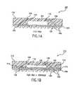
- FIG. 1Aillustrates a flex BGA package 100 .
- Flex BGA package 100includes an IC die 102 , a tape substrate 104 , a plurality of solder balls 106 , and one or more wire bonds 108 .
- Tape or flex BGA packagesare particularly appropriate for large IC dies with large numbers of inputs and outputs, such as application specific integrated circuits (ASIC) and microprocessors.
- ASICapplication specific integrated circuits
- Tape substrate 104is generally made from one or more conductive layers bonded with a dielectric material.
- the dielectric materialmay be made from various substances, such as polyimide tape.
- the conductive layersare typically made from a metal, or combination of metals, such as copper and aluminum. Trace or routing patterns are made in the conductive layer material.
- Substrate 104may be a single-layer tape, a two-layer tape, or additional layer tape substrate type. In a two-layer tape, the metal layers sandwich the dielectric layer, such as in a copper-Upilex-copper arrangement.
- IC die 102is attached directly to substrate 104 , for example, by an epoxy.
- IC die 102is any type of semiconductor IC.
- One or more wire bonds 108connect corresponding bond pads 118 on IC die 102 to contact pads or points 120 on substrate 104 .
- An encapsulate 116such as a mold compound, epoxy, or other encapsulating material, covers IC die 102 and wire bonds 108 for mechanical and environmental protection.
- flex BGA package 100does not include a stiffener.
- a stiffenercan be attached to the substrate to add planarity and rigidity to the package.
- FIG. 1Billustrates a flex BGA package 110 , similar to flex BGA package 100 , that incorporates a stiffener 112 .
- Stiffener 112may be laminated or otherwise attached to substrate 104 .
- Stiffener 112is typically made from a metal, or combination of metals, such as copper, tin, and aluminum, or may be made from a polymer and other materials, for example.
- Stiffener 112also may act as a heat sink, and allow for greater heat spreading in BGA package 110 .
- One or more openings 114 in stiffener 112may be used to allow for wire bonds 108 to connect IC die 102 to substrate 104 .
- Stiffener 112may be configured in other ways, and have different opening arrangements than shown in FIG. 1 B.
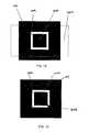
- FIG. 2Ashows a top view of a stiffener 112 .
- Stiffener 112includes an opening 114 adjacent to all four sides of an IC die mounting position 202 in the center of stiffener 112 .
- FIG. 2Bshows a temperature distribution 204 of a stiffener, such as stiffener 112 , during operation of an IC die in a flex BGA package. Temperature distribution 204 shows that heat transfer from IC die mounting position 202 to the edges of stiffener 112 is substantially limited by openings 114 . Openings 114 act as thermal barriers to heat spreading in stiffener 112 .
- FIG. 2Cshows a top view of an alternative configuration for stiffener 112 , according to an embodiment of the present invention.
- Stiffener 112includes an opening 206 adjacent to all four sides of an IC die mounting position 202 in the center of stiffener 112 . Openings 206 are similar to openings 114 of FIG. 2A, but have a different shape. The different shape can enhance thermal transfer to the outer areas of stiffener 112 , for example. Further alternatively shaped openings in stiffener 112 are applicable to the present invention, including elliptical or rounded openings, etc.
- FIG. 3shows a cross-sectional view of a conventional die-up PBGA package 300 .
- PBGA package 300includes a plastic substrate 302 , an IC die 304 , a plurality of solder balls 306 , a plurality of wire bonds 308 , a die pad 310 , one or more vias 314 , and one or more thermal/ground vias 316 .
- Plastic substrate 302includes one or more metal layers formed on an organic substrate.
- plastic or organic substratesmay include materials such as “BT”, which includes a resin called bis-maleimide triazine, and/or “FR-4,” which is a fire-retardant epoxy resin-glass cloth laminate material, and/or other similar materials.
- IC die 304is mounted to die pad 310 .
- IC die 304may be attached to die pad 310 with an epoxy, such as a silver-filled epoxy.
- Wire bonds 308connect signals of IC die 304 to substrate 302 . For instance, gold bonding wire is bonded from aluminum bond pads on IC die 304 to gold-plated contact pads on substrate 302 .
- the contact pads on substrate 302connect to solder balls 306 attached to the bottom surface of substrate 302 , through vias 314 and routing within substrate 302 using copper conductors 312 .
- Thermal/ground vias 316connect die pad 310 to one or more thermal/ground balls 322 on the center bottom surface of substrate 302 .
- An encapsulate, mold compound, or epoxy 320covers IC die 304 and wire bonds 308 for mechanical and environmental protection.
- a BGA packageincludes an array of solder balls located on a bottom external surface of the package substrate.
- FIG. 4Aillustrates a cross-sectional view of a die-up BGA package 400 .
- FIGS. 4B and 4Cillustrate exemplary solder ball arrangements for die-up BGA package 400 .
- BGA package 400includes an IC die 408 mounted on a substrate 412 .
- IC die 408is electrically connected to substrate 412 by one or more wire bonds 410 .
- Wire bonds 410are electrically connected to solder balls 406 underneath substrate 412 through corresponding vias and routing in substrate 412 .
- the vias in substrate 412can be filled with a conductive material, such as solder, to enhance these connections.
- Solder balls 406are attached to substrate 412 , and are used to attach the BGA package to a PCB.
- wire bondssuch as wire bonds 410
- IC diesmay be mounted and coupled to a substrate with solder balls located on the bottom surface of the IC die, by a process commonly referred to as “C4” or “flip chip” packaging.
- solder balls 406may be arranged in an array.
- FIG. 4Bshows a 14 by 14 array of solder balls on the bottom surface of BGA package 400 .
- Other sized arrays of solder ballsare also applicable to the present invention.
- Solder balls 406are reflowed to attach BGA package 400 to a PCB.
- the PCBmay include contact pads to which solder balls 406 are bonded.
- PCB contact padsare generally made from a metal or combination of metals, such as copper, nickel, tin, and gold.
- FIG. 4Cshows a bottom view of BGA package 400 , with an alternative solder ball array arrangement.
- BGA package 400attaches an array of solder balls 406 on a bottom surface of substrate 412 .
- solder balls 406are located in a peripheral area of the bottom surface of substrate 412 , away from a substrate center 424 .
- solder balls 406 on the bottom surface of substrate 412may be located outside an outer profile area of an IC die mounted on the opposite surface of substrate 412 .
- the solder ball arraymay be organized in any number of ways, according to the requirements of the particular BGA package application.
- the solder ball arrangement shown in FIG. 4Cis particularly applicable to embodiments of the present invention described below, such as for attaching a heat spreader/heat sink/heat slug/thermal connector to a bottom surface of a BGA package.
- the heat spreader/heat sink/heat slug/thermal connectormay be connected in substrate center 424 , for example.
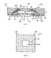
- FIG. 6shows a cross-sectional view of an example BGA package 600 , with a heat spreader 602 attached to a bottom surface.
- heat spreader 602is attached to a bottom surface of stiffener 112 through an opening 604 in substrate 104 .
- FIG. 7shows a bottom view of BGA package 600 , with heat spreader 602 attached to stiffener 112 through opening 604 .
- Heat spreader 602is attached to stiffener 112 by an adhesive material 610 .
- Heat spreader 602may be made from a metal, such as copper, aluminum, and additional metals and combinations/alloys thereof.
- heat spreader 602may be made of other electrically and/or thermally conductive materials.
- Heat spreader 602is typically thermally conductive, and therefore aids the transfer of heat generated during operation of IC die 102 out of BGA package 600 .
- heat spreader 602may also be referred to as a heat sink, a heat slug, and a thermal connector.
- Heat from IC die 102is allowed to conduct through stiffener 112 to heat spreader 602 .
- a bottom surface 606 of heat spreader 602may be attached to a printed circuit board (PCB), to transfer heat from heat spreader 602 to the PCB.
- Heat spreader 602may also be electrically conductive, and therefore may be used as a ground, power, or other signal plane for BGA package 600 .
- One or more wire bonds 608may couple these electrical signals from IC die 102 to heat spreader 602 .
- the BGA package substrateprovides electrically conductive vias and routing on one or more electrically conductive layers to connect contact pads for wire bonds on its upper surface to solder balls attached to the bottom substrate surface.
- FIG. 5shows solder ball pads and routing 504 in an example bottom substrate layer 502 .
- FIG. 8shows an example panel 800 of stiffeners 112 , according to an embodiment of the present invention.
- FIG. 9shows an example panel 900 of substrates 104 , according to an embodiment of the present invention.
- Panel 800includes six stiffeners 112 a - 112 f
- panel 900shows six substrates 104 a - 104 f .
- the present inventionis applicable to panels having any number of stiffeners 112 /substrates 104 for assembling any number of BGA packages.
- substrates 104 a - 104 feach include a centrally located opening 604 .
- panel 900is attached to panel 800 to form a combined stiffener strip/substrate strip panel. Further assembly process steps may be directed to the combined stiffener strip/substrate strip panel, including, for example: (i) attachment of the IC die to each stiffener/substrate combination in the combined panel, (ii) attachment of wire bonds between the IC die and contact pads on the substrate for each stiffener/substrate combination in the combined panel, (iii) encapsulation of the IC die and wire bonds for environmental protection for each stiffener/substrate combination in the combined panel, and/or (iv) attachment of solder balls to the substrate to each stiffener/substrate combination in the combined panel.
- the present inventionis directed to reducing harm to IC dies and other BGA package elements during assembly process steps, and to improving assembly process yields, for BGA packages produced singly or in a group.
- the present inventionis also applicable to improving thermal, mechanical, and electrical performance in the BGA package types described herein, and in other BGA package types.
- enhancements to an assembly or fabrication process for a BGA packageare provided, through the introduction of IC die support structures.
- This sectionprovides embodiments and description of IC die support structures of the present invention.
- the present inventionis described below in the context of elements of BGA packages 100 and 110 of FIGS. 1A and 1B, but the present invention is not limited to these example BGA package types.
- the present inventionis applicable to all types of BGA packages, including tape and plastic substrate packages such as BGA packages 100 , 110 , and 300 described above, ceramic substrate BGA packages, and other BGA package types.
- FIG. 10Ashows an example cross-sectional view of a mounting process for an IC die 102 .
- stiffener 112has been attached to substrate 104 , which resides against a support surface 1000 .
- Support surface 1000may or may not be present during assembly of the BGA package.
- IC die 102is being moved toward the top surface of stiffener 112 .
- FIG. 10Bshows the IC die 102 contacting the top surface of stiffener 112 .
- Arrows 1002represent a downward force being exerted on IC die 102 while being mounted to stiffener 112 .
- IC die 102may be forced and held down on stiffener 112 for a period of time to allow an adhesive material to adhere IC die 102 to stiffener 112 .
- Similar localized forcesmay also be applied to bond pads on IC die 102 during BGA package assembly processes, including attachment of wire bonds, such as is shown in FIG. 10 C.
- stiffener 112has become deformed (e.g., curved) due to the applied force.
- attachment of a wire bond 108 to a bond pad of IC die 102can also deform stiffener 112 .
- the resulting curvaturemay be temporary or permanent.
- the outer edges of stiffener 112curve away from the outer edges of substrate 104 , which may detach or weaken the attachment of stiffener 112 to substrate 104 .
- the center region of stiffener 112which has no underlying support due to opening 604 in substrate 104 , has become “bowl” shaped.
- This bowl shape for the center region of stiffener 112may cause damage to IC die 102 .
- IC die 102is being forced downward (such as shown by arrows 1002 ) onto stiffener 112 , a lack of support for the center of IC die 102 exists in the center of the “bowl.” Hence, IC die 102 may warp and/or develop one or more cracks due to the lack of uniform support, causing IC die 102 to become inoperable.
- FIG. 11illustrates a cross-sectional view of an example IC die support structure that at least partially relieves stresses to and deformation of elements of a BGA package, according to an embodiment of the present invention.
- an IC die support structure 1100has been introduced to the mounting configuration shown in FIGS. 10A-10C.
- IC die support structure 1100resides in opening 604 , between the bottom surface of stiffener 112 and support surface 1000 (when present).
- IC die support structure 1100gives support to stiffener 112 when IC die 102 is being mounted to stiffener 112 , and during further assembly process operations on IC die 102 . These include wire bond attachment and encapsulation processes, for example.
- force 1002 on IC die 102causes relatively little or no deformation to stiffener 112 . Hence, harm to stiffener 112 and IC die 102 is reduced or eliminated.
- IC die support structure 1100is removably held in opening 604 . As described below, IC die support structure 1100 may be removed from opening 604 after the relevant assembly process steps have been completed.
- IC die support structure 1100is substantially co-planar with substrate 104 , and has substantially the same rectangular shape as opening 604 (such as shown for opening 604 in FIG. 7 ). Furthermore, IC die support structure 1100 has a thickness that is substantially equal to a thickness of substrate 104 . In this manner, IC die support structure 1100 fits within opening 604 between stiffener 112 and support surface 1000 (when present), and provides sufficient support to stiffener 112 during assembly operations. In alternative embodiments, IC die support structure 1100 may have shapes other than rectangular, including circular, for example. Furthermore, IC die support structure 1100 may have a shape different than that of opening 604 , including round or elliptical, and any polygon, for example. Still further, IC die support structure 1100 may have other sizes, including having greater or less thickness than substrate 104 .
- Example embodiments for holding IC die support structure 1100 in opening 604are further described as follows. These examples are provided for illustrative purposes, and the present invention is not limited to these examples. These embodiments for holding IC die support structure 1100 may be used with or without support surface 1000 shown in FIG. 10 A. Further mechanisms for holding IC die support structure 1100 in opening 604 will be apparent to persons skilled in the relevant art(s) from the teachings herein.
- FIG. 12illustrates a top, plan view of substrate 104 having an example IC die support structure 1100 , according to an embodiment of the present invention.
- substrate 104has opening 604 located in a central region of substrate 104 . Opening 604 is open at the top and bottom surfaces of substrate 104 .
- IC die support structure 1100is removably held in opening 604 .
- IC die support structure 1100is considered removably held in opening 604 because it is attached to an adhesive tape 1202 , which is attached to, and may be detached from substrate 104 .
- Adhesive tape 1202is attached to substrate 104 , and holds IC die support structure 1100 in opening 604 .
- adhesive tape 1202may be detached from the corresponding substrate 104 . Detaching adhesive tape 1202 from substrate 104 removes IC die support structure 1100 from opening 604 .
- Adhesive tape 1202may also be a rigid planar carrier, such as a plate, etc. In such an embodiment, IC die support structure 1100 may be attached to the rigid planar carrier by an adhesive material, such as an adhesive tape, or by other mechanism, including removable and non-removable means.
- IC die support structure 1100 as shown in FIG. 12provides support to stiffener 112 while IC die 102 is being mounted thereto, and while additional assembly processes are being executed on the respective BGA package.
- Adhesive tape 1202may be any type of tape having an adhesive material on at least one surface.
- adhesive tape 1202may be of a size to attach a single IC die support structure 1100 to a single substrate 104 .
- a single strip of adhesive tape 1202may be of a size to attach a plurality of IC die supports 1100 to a plurality of substrates 104 , such as in substrate strip 900 .
- IC die support structure 1100can be attached to adhesive tape 1202 at any time before, during, or after adhesive tape 1202 is attached to substrate 104 .
- FIG. 13illustrates a view of substrate 104 with another example IC die support structure 1100 , according to embodiments of the present invention.
- substrate 104has opening 604 located in a central region that is open at the top and bottom surfaces of substrate 104 .
- IC die support structure 1100 shown in FIG. 13is removably held in opening 604 .
- IC die support structure 1100is considered removably held in opening 604 because it is held in opening 604 by a breakable stud or tab 1302 .
- Tab 1302may be broken to release IC die support structure 1100 from opening 604 . Once IC die support structure 1100 is released by breaking tab 1302 , it may be physically removed or may be allowed to drop from opening 604 on its own.
- tab 1302is made from a material external from substrate 104 that is positioned in opening 604 to hold IC die support structure 1100 .
- tab 1302 and IC die support structure 1100are portions of substrate 104 that remain in opening 604 when opening 604 is formed in substrate 104 .
- tab 1302 and IC die support structure 1100may be formed with opening 604 in substrate 104 by cutting a non-continuous line in the shape of a rectangle, or other shape, through substrate 104 in a center region. The substrate material that is removed during the cutting process is removed from the gap formed between substrate 104 and IC die support structure 1100 .
- opening 604may be formed around IC die support structure and tab 1302 by sawing, cutting, drilling, machining, by laser, and other ways.
- IC die support structure 1100 as shown in FIG. 13provides support to stiffener 112 while IC die 102 is being mounted thereto, and while additional assembly processes are being executed on the respective BGA package.
- the example embodiment of FIG. 13shows a single tab 1300 located in a corner of opening 604 , that removably holds IC die support structure 1100 in opening 604 .
- FIGS. 14 and 15illustrate views of substrate 104 with IC die support structure 1100 removably held by one or more tabs 1302 , according to further embodiments of the present invention.
- FIG. 14shows a first tab 1302 a removably holding IC die support structure 1100 in a first corner of opening 604 , and a second tab 1302 b removably holding IC die support structure 1100 in a second corner of opening 604 .
- FIG. 15shows tab 1302 removably holding IC die support structure 1100 to a middle area of an edge of opening 604 . Any number of one or more tabs 1302 may be used to removably hold IC die support structure 1100 in opening 604 . Furthermore, the one or more tabs 1302 may be located anywhere in the corners or along the edges of opening 604 .
- IC die support structure 1100may be a substrate portion formed from opening 604 of substrate 104 , and hence be made from the same material as substrate 104 .
- IC die support structure 1100can be made from a substrate material that is the same as or different from that of substrate 104 . These substrate materials include tape, plastic, and/or ceramic substrate materials.
- IC die support structure 1100may be made from a plastic material, such as BT and/or FR 4 , and/or a ceramic.
- IC die support structure 1100can also be made from a metal, such as copper, aluminum, tin, nickel, iron, other metals, and combinations/alloys thereof.
- IC die support structure 1100may be made from other materials as well.
- FIG. 16shows a flowchart 1600 providing steps for assembling a BGA package according to one or more embodiments of the present invention.
- Other operational and structural embodimentswill be apparent to persons skilled in the relevant art(s) based on the following discussion. These steps are described in detail below.
- Flowchart 1600begins with step 1602 .
- a stiffeneris attached to a substrate that has a centrally located opening that is open therethrough and has an integrated circuit (IC) die support structure removably held therein.
- the stiffeneris stiffener 112 and the substrate is substrate 104 , which are attached to each other, as shown in FIG. 11 .
- substrate 104as a centrally located opening 604 that is open at the top and bottom surfaces of substrate 104 .
- opening 604has IC die support structure 1100 removably positioned therein.
- an IC dieis mounted to a central region of the stiffener.
- IC die 102is mounted to the top surface of stiffener 112 , in a central region that is opposite to opening 604 in substrate 104 .
- step 1606the IC die support structure is removed from the centrally located opening. For example, as described above, after one or more assembly operations are performed on the BGA package, IC die support structure 1100 is removed from opening 604 .
- step 1604includes the step where the IC die support structure is allowed to support the central region of the stiffener while the IC die is being mounted to the central region of the stiffener.
- IC die support structure 1100supports stiffener 112 in the region adjacent to opening 604 in substrate 104 when assembly operations are performed that involve forces upon IC die 102 , such as mounting IC die 102 to stiffener 112 , attaching wire bonds 108 / 608 , and applying encapsulate 116 .
- flowchart 1600may include the additional step where an adhesive tape is applied to the substrate to which the IC die support structure is attached so that the IC die support structure is removably held within the centrally located opening.
- the adhesive tapeis adhesive tape 1202 , as shown in FIG. 12 .
- Adhesive tape 1202has IC die support structure 1100 attached thereto, and is applied to substrate 104 .
- IC die support structure 1100is located and removably held in opening 604 by adhesive tape 1202 .
- step 1606may include the step where the applied adhesive tape is detached from the substrate to remove the IC die support structure from the centrally located opening.
- adhesive tape 1202may be removed from substrate 104 . Because IC die support structure 1100 is attached to adhesive tape 1202 , IC die support structure 1100 is removed from opening 604 when adhesive tape 1202 is detached.
- FIG. 17Ashows a flowchart 1700 providing steps for assembling a plurality of BGA packages according to one or more embodiments of the present invention.
- FIG. 17Bprovides additional optional steps, according to further embodiments of the present invention.
- Other operational and structural embodimentswill be apparent to persons skilled in the relevant art(s) based on the following discussion. These steps are described in detail below.
- Flowchart 1700begins with step 1702 .
- a substrate stripthat includes a plurality of substrates that each include a centrally located opening with an IC die support structure removably held therein is formed.
- the substrate stripis substrate strip 900 , as shown in FIG. 9 .
- Substrate strip 900includes a plurality of substrates 104 , that each include an opening 604 .
- stiffener strip 900is formed so that each substrate of the plurality of substrates 104 include an IC die support structure 1100 removably held therein.
- a stiffener strip that includes a plurality of stiffenersis attached to the substrate strip such that a first surface of each stiffener of the plurality of stiffeners is attached to a first surface of a corresponding substrate of the plurality of substrates.
- the stiffener stripis stiffener strip 800 , as shown in FIG. 8 .
- stiffener strip 800includes a plurality of stiffeners 112 .
- Substrate strip 900 and stiffener strip 800are attached to each other to form a substrate strip/stiffener strip combination.
- an IC dieis mounted to a central region of a second surface of each stiffener of the plurality of stiffeners.
- an IC die 102is mounted to the top surface of each stiffener of the plurality of stiffeners 112 of stiffener strip 800 , in a central region that is opposite to opening 604 in the respective substrate 104 .
- a bond pad of the IC die mounted to each stiffener of the plurality of stiffenersis connected to a contact pad on the first surface of the corresponding substrate of the plurality of substrates with a wire bond.
- a wire bond 108may be used to connect a bond pad of IC die 102 to a contact pad on the top surface of substrate 104 , for each IC die 102 and each corresponding substrate of the plurality of substrates 104 .
- step 1710the IC die and the wire bond are encapsulated on the second surface of each stiffener of the plurality of stiffeners.
- an encapsulate 116may be applied to the BGA package to encapsulate IC die 102 and wire bonds 108 / 608 to the top surface of each stiffener of the plurality of stiffeners 112 .
- the IC die support structureis removed from the centrally located opening of each substrate of the plurality of substrates. For example, as described above for a single IC die support structure 1100 , after one or more assembly operations are performed on the substrate strip/stiffener strip combinations, IC die support structure 1100 is removed from each opening 604 .
- steps 1706 , 1708 , and 1710include the step where the IC die support structure is allowed to support the central region of the stiffener during the respective step(s).
- the assembly processes described aboveplace respective forces upon IC die 102 .
- IC die support structure 1100supports stiffener 112 during these assembly process steps to prevent substantial deformation of stiffener 112 , and damage to IC die 102 .
- step 1702may include the step where an adhesive tape to which a plurality of IC die support structures are attached is applied to the substrate strip so that an IC die support structure of the plurality of IC die support structures is removably held within the centrally located opening of each substrate of the plurality of substrates.
- the adhesive tapeis adhesive tape 1202 , as shown for a single substrate 104 in FIG. 12 .
- Adhesive tape 1202has IC die support structure 1100 for each opening 604 attached thereto, and is applied to substrate strip 900 .
- An IC die support structure 1100is located and removably held in each opening 604 by adhesive tape 1202 .
- a single adhesive tape 1202may removably hold all IC die support structures 1100 , or a separate adhesive tape 1202 may be used for each IC die support structure 1100 in the substrate strip/stiffener strip combination.
- step 1712may include the step where the applied adhesive tape is detached from the substrate strip to remove the IC die support structure held within the centrally located opening of each substrate of the plurality of substrates.
- adhesive tape 1202may be removed from the plurality of substrates 104 . Because each IC die support structure 1100 is attached to adhesive tape 1202 , each IC die support structure 1100 is removed from the respective opening 604 .
- step 1702may include the step where the centrally located opening is formed in each substrate of the plurality of substrates such that a substrate portion remains removably held in the centrally located opening of each substrate of the plurality of substrates by at least one substrate tab as the IC die support structure.
- opening 604may be formed for each substrate in the plurality of substrates 104 such that a portion of the substrate remains within each opening 604 as IC die support structure 1100 .
- At least one substrate tab, such as tab 1302removably holds IC die support structure 1100 in each opening 604 .
- step 1712may include the step where the at least one substrate tab removably holding the substrate portion in the centrally located opening of each substrate of the plurality of substrates is broken to release the IC die support structure removably held within the centrally located opening of each substrate of the plurality of substrates.
- a respective tab 1302may be broken to release IC die support structure 1100 in each opening 604 , so that each IC die support structure 1100 may be removed.
- FIG. 17Bshows additional steps for flowchart 1700 .
- any number of one or more steps shown in FIG. 17Bmay be combined with flowchart 1700 shown in FIG. 17 A.
- flowchart 1700may include the additional step of step 1714 , as shown in FIG. 17 B.
- a heat spreaderis mounted to a central region of the first surface of each stiffener of the plurality of stiffeners through the centrally located opening in each substrate of the plurality of substrates. For example, as shown in FIG.
- a heat spreader 602may be coupled to each stiffener 112 through the opening 604 in the respective substrate 104 for each substrate/stiffener combination in the substrate strip/stiffener strip combination, after removal of IC die support structures 1100 .
- flowchart 1700may include the additional step of step 1716 , as shown in FIG. 17 B.
- step 1716a plurality of solder balls are attached to a second surface of each substrate of the plurality of substrates.
- a plurality of solder balls 106may be applied to the bottom surface of substrate 104 .
- flowchart 1700may include the additional step of step 1718 , as shown in FIG. 17 B.
- step 1718a substrate/stiffener strip formed by attaching the stiffener strip to the substrate strip in step 1704 is singulated into a plurality of separate BGA packages.
- each stiffener/substrate combinationmay be separated from the stiffener strip/substrate strip combination to form a plurality of BGA packages. Sawing, cutting, machining, and other processes may be used to perform the separation.
Landscapes
- Engineering & Computer Science (AREA)
- Microelectronics & Electronic Packaging (AREA)
- Power Engineering (AREA)
- Computer Hardware Design (AREA)
- General Physics & Mathematics (AREA)
- Condensed Matter Physics & Semiconductors (AREA)
- Physics & Mathematics (AREA)
- Manufacturing & Machinery (AREA)
- Ceramic Engineering (AREA)
- Chemical & Material Sciences (AREA)
- Materials Engineering (AREA)
- Die Bonding (AREA)
- Wire Bonding (AREA)
- Cooling Or The Like Of Semiconductors Or Solid State Devices (AREA)
Abstract
Description
Claims (18)
Priority Applications (2)
| Application Number | Priority Date | Filing Date | Title |
|---|---|---|---|
| US10/284,349US6825108B2 (en) | 2002-02-01 | 2002-10-31 | Ball grid array package fabrication with IC die support structures |
| US10/899,144US7078806B2 (en) | 2002-02-01 | 2004-07-27 | IC die support structures for ball grid array package fabrication |
Applications Claiming Priority (2)
| Application Number | Priority Date | Filing Date | Title |
|---|---|---|---|
| US35287702P | 2002-02-01 | 2002-02-01 | |
| US10/284,349US6825108B2 (en) | 2002-02-01 | 2002-10-31 | Ball grid array package fabrication with IC die support structures |
Related Child Applications (1)
| Application Number | Title | Priority Date | Filing Date |
|---|---|---|---|
| US10/899,144ContinuationUS7078806B2 (en) | 2002-02-01 | 2004-07-27 | IC die support structures for ball grid array package fabrication |
Publications (2)
| Publication Number | Publication Date |
|---|---|
| US20030146506A1 US20030146506A1 (en) | 2003-08-07 |
| US6825108B2true US6825108B2 (en) | 2004-11-30 |
Family
ID=27668557
Family Applications (2)
| Application Number | Title | Priority Date | Filing Date |
|---|---|---|---|
| US10/284,349Expired - LifetimeUS6825108B2 (en) | 2002-02-01 | 2002-10-31 | Ball grid array package fabrication with IC die support structures |
| US10/899,144Expired - LifetimeUS7078806B2 (en) | 2002-02-01 | 2004-07-27 | IC die support structures for ball grid array package fabrication |
Family Applications After (1)
| Application Number | Title | Priority Date | Filing Date |
|---|---|---|---|
| US10/899,144Expired - LifetimeUS7078806B2 (en) | 2002-02-01 | 2004-07-27 | IC die support structures for ball grid array package fabrication |
Country Status (1)
| Country | Link |
|---|---|
| US (2) | US6825108B2 (en) |
Cited By (33)
| Publication number | Priority date | Publication date | Assignee | Title |
|---|---|---|---|---|
| US20040159928A1 (en)* | 2002-11-22 | 2004-08-19 | Infineon Technologies Ag | Supporting structure for a chip and method for producing the same |
| US20040241914A1 (en)* | 2001-10-24 | 2004-12-02 | Intel Corporation | Mechanical support system for a thin package |
| US20050090043A1 (en)* | 2003-10-24 | 2005-04-28 | Advanced Semiconductor Engineering, Inc. | Manufacturing method of ball grid array package |
| US20050161781A1 (en)* | 2003-12-24 | 2005-07-28 | Sanyo Electric Co., Ltd. | Hybrid integrated circuit device and manufacturing method thereof |
| US20050173787A1 (en)* | 2002-03-21 | 2005-08-11 | Broadcom Corporation | Method for assembling a ball grid array package with two substrates |
| US20050280127A1 (en)* | 2004-06-21 | 2005-12-22 | Broadcom Corporation | Apparatus and method for thermal and electromagnetic interference (EMI) shielding enhancement in die-up array packages |
| US20070040267A1 (en)* | 2005-08-22 | 2007-02-22 | Broadcom Corporation | Method and system for secure heat sink attachment on semiconductor devices with macroscopic uneven surface features |
| US20070090502A1 (en)* | 2005-10-20 | 2007-04-26 | Broadcom Corporation | Methods and apparatus for improved thermal performance and electromagnetic interference (EMI) shielding in leadframe integrated circuit (IC) packages |
| US20070164451A1 (en)* | 2006-01-19 | 2007-07-19 | Anwar Ali | Power configuration method for structured ASICs |
| US20070253179A1 (en)* | 2006-04-27 | 2007-11-01 | Briggs Randall D | Method and apparatus for removing surface mount device from printed circuit board |
| US20070267740A1 (en)* | 2006-05-16 | 2007-11-22 | Broadcom Corporation | Method and apparatus for cooling semiconductor device hot blocks and large scale integrated circuit (IC) using integrated interposer for IC packages |
| US20070273023A1 (en)* | 2006-05-26 | 2007-11-29 | Broadcom Corporation | Integrated circuit package having exposed thermally conducting body |
| US20070290322A1 (en)* | 2006-06-20 | 2007-12-20 | Broadcom Corporation | Thermal improvement for hotspots on dies in integrated circuit packages |
| US20080006934A1 (en)* | 2004-11-03 | 2008-01-10 | Broadcom Corporation | Flip Chip Package Including a Non-Planar Heat Spreader and Method of Making the Same |
| US20080012152A1 (en)* | 2006-07-11 | 2008-01-17 | Thorsten Meyer | Component and method for producing a component |
| US20080096312A1 (en)* | 2006-10-20 | 2008-04-24 | Broadcom Corporation | Low profile ball grid array (BGA) package with exposed die and method of making same |
| US20080099898A1 (en)* | 2006-10-27 | 2008-05-01 | Compass Technology Co., Ltd. | Die-up integrated circuit package with grounded stiffener |
| US20080169489A1 (en)* | 2006-10-27 | 2008-07-17 | Robert Raymond Petkovsek | Multi-walled tube and method of manufacture |
| US20080211089A1 (en)* | 2007-02-16 | 2008-09-04 | Broadcom Corporation | Interposer for die stacking in semiconductor packages and the method of making the same |
| US7462933B2 (en) | 2000-12-22 | 2008-12-09 | Broadcom Corporation | Ball grid array package enhanced with a thermal and electrical connector |
| US20080303124A1 (en)* | 2007-06-08 | 2008-12-11 | Broadcom Corporation | Lead frame-BGA package with enhanced thermal performance and I/O counts |
| US7482686B2 (en) | 2004-06-21 | 2009-01-27 | Braodcom Corporation | Multipiece apparatus for thermal and electromagnetic interference (EMI) shielding enhancement in die-up array packages and method of making the same |
| US7579217B2 (en) | 2000-12-22 | 2009-08-25 | Broadcom Corporation | Methods of making a die-up ball grid array package with printed circuit board attachable heat spreader |
| US7714453B2 (en) | 2006-05-12 | 2010-05-11 | Broadcom Corporation | Interconnect structure and formation for package stacking of molded plastic area array package |
| US7781882B2 (en) | 2002-03-22 | 2010-08-24 | Broadcom Corporation | Low voltage drop and high thermal performance ball grid array package |
| US7808087B2 (en) | 2006-06-01 | 2010-10-05 | Broadcom Corporation | Leadframe IC packages having top and bottom integrated heat spreaders |
| US8021927B2 (en) | 2004-09-29 | 2011-09-20 | Broadcom Corporation | Die down ball grid array packages and method for making same |
| US8183680B2 (en) | 2006-05-16 | 2012-05-22 | Broadcom Corporation | No-lead IC packages having integrated heat spreader for electromagnetic interference (EMI) shielding and thermal enhancement |
| US8581381B2 (en) | 2006-06-20 | 2013-11-12 | Broadcom Corporation | Integrated circuit (IC) package stacking and IC packages formed by same |
| US20160050771A1 (en)* | 2014-08-15 | 2016-02-18 | Unimicron Technology Corp. | Manufacturing method of circuit structure embedded with heat-dissipation block |
| US11296005B2 (en)* | 2019-09-24 | 2022-04-05 | Analog Devices, Inc. | Integrated device package including thermally conductive element and method of manufacturing same |
| US11769752B2 (en)* | 2020-07-24 | 2023-09-26 | Micron Technology, Inc. | Stacked semiconductor die assemblies with substrate heat sinks and associated systems and methods |
| US12315776B2 (en) | 2021-11-08 | 2025-05-27 | Analog Devices, Inc. | Integrated device package with an integrated heat sink |
Families Citing this family (19)
| Publication number | Priority date | Publication date | Assignee | Title |
|---|---|---|---|---|
| AU2002217987A1 (en)* | 2000-12-01 | 2002-06-11 | Broadcom Corporation | Thermally and electrically enhanced ball grid array packaging |
| US6906414B2 (en)* | 2000-12-22 | 2005-06-14 | Broadcom Corporation | Ball grid array package with patterned stiffener layer |
| US6853070B2 (en)* | 2001-02-15 | 2005-02-08 | Broadcom Corporation | Die-down ball grid array package with die-attached heat spreader and method for making the same |
| US7259448B2 (en)* | 2001-05-07 | 2007-08-21 | Broadcom Corporation | Die-up ball grid array package with a heat spreader and method for making the same |
| US6879039B2 (en) | 2001-12-18 | 2005-04-12 | Broadcom Corporation | Ball grid array package substrates and method of making the same |
| US6861750B2 (en) | 2002-02-01 | 2005-03-01 | Broadcom Corporation | Ball grid array package with multiple interposers |
| US6825108B2 (en)* | 2002-02-01 | 2004-11-30 | Broadcom Corporation | Ball grid array package fabrication with IC die support structures |
| US7037805B2 (en)* | 2003-05-07 | 2006-05-02 | Honeywell International Inc. | Methods and apparatus for attaching a die to a substrate |
| US7411281B2 (en)* | 2004-06-21 | 2008-08-12 | Broadcom Corporation | Integrated circuit device package having both wire bond and flip-chip interconnections and method of making the same |
| US7190068B2 (en)* | 2004-06-25 | 2007-03-13 | Intel Corporation | Bottom heat spreader |
| US7491567B2 (en)* | 2005-11-22 | 2009-02-17 | Honeywell International Inc. | MEMS device packaging methods |
| US20070246822A1 (en)* | 2006-04-25 | 2007-10-25 | Glover Kerry C | Hard disk drive preamp heat dissipation methods |
| US7985621B2 (en)* | 2006-08-31 | 2011-07-26 | Ati Technologies Ulc | Method and apparatus for making semiconductor packages |
| US20080169551A1 (en)* | 2007-01-16 | 2008-07-17 | Powertech Technology Inc. | IC chip package with near substrate scale chip attachment |
| KR100856209B1 (en)* | 2007-05-04 | 2008-09-03 | 삼성전자주식회사 | Printed circuit board with integrated circuit and manufacturing method |
| US8450151B1 (en)* | 2011-11-22 | 2013-05-28 | Texas Instruments Incorporated | Micro surface mount device packaging |
| US20160035593A1 (en)* | 2014-07-31 | 2016-02-04 | Skyworks Solutions, Inc. | Devices and methods related to support for packaging substrate panel having cavities |
| US9832860B2 (en)* | 2014-09-26 | 2017-11-28 | Intel Corporation | Panel level fabrication of package substrates with integrated stiffeners |
| CN113466660B (en)* | 2021-06-28 | 2022-09-30 | 中国科学技术大学 | A reliability detection method of board-level BGA package under fire smoke |
Citations (113)
| Publication number | Priority date | Publication date | Assignee | Title |
|---|---|---|---|---|
| US3790866A (en) | 1973-05-14 | 1974-02-05 | Gen Motors Corp | Semiconductor device enclosure and method of making same |
| US4611238A (en) | 1982-05-05 | 1986-09-09 | Burroughs Corporation | Integrated circuit package incorporating low-stress omnidirectional heat sink |
| US5045921A (en) | 1989-12-26 | 1991-09-03 | Motorola, Inc. | Pad array carrier IC device using flexible tape |
| US5065281A (en)* | 1990-02-12 | 1991-11-12 | Rogers Corporation | Molded integrated circuit package incorporating heat sink |
| US5173766A (en) | 1990-06-25 | 1992-12-22 | Lsi Logic Corporation | Semiconductor device package and method of making such a package |
| US5208504A (en) | 1990-12-28 | 1993-05-04 | Raytheon Company | Saw device and method of manufacture |
| US5216278A (en) | 1990-12-04 | 1993-06-01 | Motorola, Inc. | Semiconductor device having a pad array carrier package |
| US5285352A (en) | 1992-07-15 | 1994-02-08 | Motorola, Inc. | Pad array semiconductor device with thermal conductor and process for making the same |
| US5291062A (en) | 1993-03-01 | 1994-03-01 | Motorola, Inc. | Area array semiconductor device having a lid with functional contacts |
| US5294826A (en) | 1993-04-16 | 1994-03-15 | Northern Telecom Limited | Integrated circuit package and assembly thereof for thermal and EMI management |
| US5366589A (en) | 1993-11-16 | 1994-11-22 | Motorola, Inc. | Bonding pad with circular exposed area and method thereof |
| US5394009A (en) | 1993-07-30 | 1995-02-28 | Sun Microsystems, Inc. | Tab semiconductor package with cushioned land grid array outer lead bumps |
| US5397917A (en) | 1993-04-26 | 1995-03-14 | Motorola, Inc. | Semiconductor package capable of spreading heat |
| US5397921A (en) | 1993-09-03 | 1995-03-14 | Advanced Semiconductor Assembly Technology | Tab grid array |
| US5433631A (en) | 1993-01-26 | 1995-07-18 | International Business Machines Corporation | Flex circuit card elastomeric cable connector assembly |
| US5438216A (en) | 1992-08-31 | 1995-08-01 | Motorola, Inc. | Light erasable multichip module |
| US5474957A (en) | 1994-05-09 | 1995-12-12 | Nec Corporation | Process of mounting tape automated bonded semiconductor chip on printed circuit board through bumps |
| US5490324A (en) | 1993-09-15 | 1996-02-13 | Lsi Logic Corporation | Method of making integrated circuit package having multiple bonding tiers |
| US5534467A (en) | 1993-03-18 | 1996-07-09 | Lsi Logic Corporation | Semiconductor packages for high I/O semiconductor dies |
| US5541450A (en) | 1994-11-02 | 1996-07-30 | Motorola, Inc. | Low-profile ball-grid array semiconductor package |
| US5552635A (en) | 1994-01-11 | 1996-09-03 | Samsung Electronics Co., Ltd. | High thermal emissive semiconductor device package |
| US5572405A (en) | 1995-06-07 | 1996-11-05 | International Business Machines Corporation (Ibm) | Thermally enhanced ball grid array package |
| US5578869A (en) | 1994-03-29 | 1996-11-26 | Olin Corporation | Components for housing an integrated circuit device |
| US5583377A (en) | 1992-07-15 | 1996-12-10 | Motorola, Inc. | Pad array semiconductor device having a heat sink with die receiving cavity |
| US5583378A (en) | 1994-05-16 | 1996-12-10 | Amkor Electronics, Inc. | Ball grid array integrated circuit package with thermal conductor |
| US5642261A (en) | 1993-12-20 | 1997-06-24 | Sgs-Thomson Microelectronics, Inc. | Ball-grid-array integrated circuit package with solder-connected thermal conductor |
| US5648679A (en) | 1994-09-16 | 1997-07-15 | National Semiconductor Corporation | Tape ball lead integrated circuit package |
| US5650659A (en) | 1995-08-04 | 1997-07-22 | National Semiconductor Corporation | Semiconductor component package assembly including an integral RF/EMI shield |
| US5691567A (en) | 1995-09-19 | 1997-11-25 | National Semiconductor Corporation | Structure for attaching a lead frame to a heat spreader/heat slug structure |
| US5717252A (en) | 1994-07-25 | 1998-02-10 | Mitsui High-Tec, Inc. | Solder-ball connected semiconductor device with a recessed chip mounting area |
| US5736785A (en) | 1996-12-20 | 1998-04-07 | Industrial Technology Research Institute | Semiconductor package for improving the capability of spreading heat |
| EP0504411B1 (en) | 1990-09-19 | 1998-06-17 | Fujitsu Limited | Semiconductor device having many lead pins |
| US5796170A (en) | 1996-02-15 | 1998-08-18 | Northern Telecom Limited | Ball grid array (BGA) integrated circuit packages |
| US5798909A (en) | 1995-02-15 | 1998-08-25 | International Business Machines Corporation | Single-tiered organic chip carriers for wire bond-type chips |
| US5801432A (en) | 1992-06-04 | 1998-09-01 | Lsi Logic Corporation | Electronic system using multi-layer tab tape semiconductor device having distinct signal, power and ground planes |
| US5835355A (en) | 1997-09-22 | 1998-11-10 | Lsi Logic Corporation | Tape ball grid array package with perforated metal stiffener |
| US5843808A (en) | 1996-01-11 | 1998-12-01 | Asat, Limited | Structure and method for automated assembly of a tab grid array package |
| US5844168A (en) | 1995-08-01 | 1998-12-01 | Minnesota Mining And Manufacturing Company | Multi-layer interconnect sutructure for ball grid arrays |
| US5856911A (en) | 1996-11-12 | 1999-01-05 | National Semiconductor Corporation | Attachment assembly for integrated circuits |
| US5866949A (en) | 1996-12-02 | 1999-02-02 | Minnesota Mining And Manufacturing Company | Chip scale ball grid array for integrated circuit packaging |
| US5883430A (en) | 1996-06-19 | 1999-03-16 | International Business Machines Corporation | Thermally enhanced flip chip package |
| US5889324A (en) | 1998-03-30 | 1999-03-30 | Nec Corporation | Package for a semiconductor device |
| US5894410A (en) | 1996-03-28 | 1999-04-13 | Intel Corporation | Perimeter matrix ball grid array circuit package with a populated center |
| US5901041A (en) | 1997-12-02 | 1999-05-04 | Northern Telecom Limited | Flexible integrated circuit package |
| US5903052A (en) | 1998-05-12 | 1999-05-11 | Industrial Technology Research Institute | Structure for semiconductor package for improving the efficiency of spreading heat |
| US5905633A (en) | 1996-02-29 | 1999-05-18 | Anam Semiconductor Inc. | Ball grid array semiconductor package using a metal carrier ring as a heat spreader |
| US5907903A (en) | 1996-05-24 | 1999-06-01 | International Business Machines Corporation | Multi-layer-multi-chip pyramid and circuit board structure and method of forming same |
| US5920117A (en) | 1994-08-02 | 1999-07-06 | Fujitsu Limited | Semiconductor device and method of forming the device |
| US5949137A (en) | 1997-09-26 | 1999-09-07 | Lsi Logic Corporation | Stiffener ring and heat spreader for use with flip chip packaging assemblies |
| US5953589A (en) | 1996-12-30 | 1999-09-14 | Anam Semiconductor Inc. | Ball grid array semiconductor package with solder balls fused on printed circuit board and method for fabricating the same |
| US5972734A (en) | 1997-09-17 | 1999-10-26 | Lsi Logic Corporation | Interposer for ball grid array (BGA) package |
| US5977626A (en) | 1998-08-12 | 1999-11-02 | Industrial Technology Research Institute | Thermally and electrically enhanced PBGA package |
| US5986340A (en) | 1996-05-02 | 1999-11-16 | National Semiconductor Corporation | Ball grid array package with enhanced thermal and electrical characteristics and electronic device incorporating same |
| US5986885A (en) | 1997-04-08 | 1999-11-16 | Integrated Device Technology, Inc. | Semiconductor package with internal heatsink and assembly method |
| US5999415A (en) | 1998-11-18 | 1999-12-07 | Vlsi Technology, Inc. | BGA package using PCB and tape in a die-down configuration |
| US5998241A (en) | 1997-12-08 | 1999-12-07 | Nec Corporation | Semiconductor device and method of manufacturing the same |
| US6002147A (en) | 1996-09-26 | 1999-12-14 | Samsung Electronics Company | Hybrid microwave-frequency integrated circuit |
| US6002169A (en) | 1998-06-15 | 1999-12-14 | Lsi Logic Corporation | Thermally enhanced tape ball grid array package |
| US6011694A (en) | 1996-08-01 | 2000-01-04 | Fuji Machinery Mfg. & Electronics Co., Ltd. | Ball grid array semiconductor package with solder ball openings in an insulative base |
| US6011304A (en) | 1997-05-05 | 2000-01-04 | Lsi Logic Corporation | Stiffener ring attachment with holes and removable snap-in heat sink or heat spreader/lid |
| US6020637A (en) | 1997-05-07 | 2000-02-01 | Signetics Kp Co., Ltd. | Ball grid array semiconductor package |
| US6028358A (en) | 1996-05-30 | 2000-02-22 | Nec Corporation | Package for a semiconductor device and a semiconductor device |
| TW383908U (en) | 1998-09-22 | 2000-03-01 | Caesar Technology Inc | Structure used for increasing heat-dissipation of micro-electronic apparatus |
| US6057601A (en) | 1998-11-27 | 2000-05-02 | Express Packaging Systems, Inc. | Heat spreader with a placement recess and bottom saw-teeth for connection to ground planes on a thin two-sided single-core BGA substrate |
| US6060777A (en) | 1998-07-21 | 2000-05-09 | Intel Corporation | Underside heat slug for ball grid array packages |
| US6069407A (en) | 1998-11-18 | 2000-05-30 | Vlsi Technology, Inc. | BGA package using PCB and tape in a die-up configuration |
| US6077724A (en) | 1998-09-05 | 2000-06-20 | First International Computer Inc. | Multi-chips semiconductor package and fabrication method |
| US6084297A (en) | 1998-09-03 | 2000-07-04 | Micron Technology, Inc. | Cavity ball grid array apparatus |
| US6084777A (en) | 1997-04-23 | 2000-07-04 | Texas Instruments Incorporated | Ball grid array package |
| US6114761A (en) | 1998-01-20 | 2000-09-05 | Lsi Logic Corporation | Thermally-enhanced flip chip IC package with extruded heatspreader |
| US6117797A (en) | 1998-09-03 | 2000-09-12 | Micron Technology, Inc. | Attachment method for heat sinks and devices involving removal of misplaced encapsulant |
| US6122171A (en) | 1999-07-30 | 2000-09-19 | Micron Technology, Inc. | Heat sink chip package and method of making |
| JP2000286294A (en) | 1999-03-30 | 2000-10-13 | Hitachi Ltd | Semiconductor device and manufacturing method thereof |
| US6133064A (en) | 1999-05-27 | 2000-10-17 | Lsi Logic Corporation | Flip chip ball grid array package with laminated substrate |
| US6140707A (en) | 1998-05-07 | 2000-10-31 | 3M Innovative Properties Co. | Laminated integrated circuit package |
| US6160705A (en) | 1997-05-09 | 2000-12-12 | Texas Instruments Incorporated | Ball grid array package and method using enhanced power and ground distribution circuitry |
| US6162659A (en) | 1999-03-05 | 2000-12-19 | International Business Machines Corporation | Method for manufacturing a package structure having a heat spreader for integrated circuit chips |
| US6163458A (en) | 1999-12-03 | 2000-12-19 | Caesar Technology, Inc. | Heat spreader for ball grid array package |
| US6166434A (en) | 1997-09-23 | 2000-12-26 | Lsi Logic Corporation | Die clip assembly for semiconductor package |
| TW417219B (en) | 1999-07-22 | 2001-01-01 | Siliconware Precision Industries Co Ltd | Ball grid array package having leads |
| US6184580B1 (en) | 1999-09-10 | 2001-02-06 | Siliconware Precision Industries Co., Ltd. | Ball grid array package with conductive leads |
| US6201300B1 (en) | 1998-04-22 | 2001-03-13 | World Wiser Electronics Inc. | Printed circuit board with thermal conductive structure |
| US6212070B1 (en) | 1996-07-22 | 2001-04-03 | International Business Machines Corporation | Zero force heat sink |
| US6242279B1 (en) | 1999-06-14 | 2001-06-05 | Thin Film Module, Inc. | High density wire bond BGA |
| US6246111B1 (en) | 2000-01-25 | 2001-06-12 | Siliconware Precision Industries Co., Ltd. | Universal lead frame type of quad flat non-lead package of semiconductor |
| US6288444B1 (en) | 1998-11-17 | 2001-09-11 | Fujitsu Limited | Semiconductor device and method of producing the same |
| US6313521B1 (en) | 1998-11-04 | 2001-11-06 | Nec Corporation | Semiconductor device and method of manufacturing the same |
| US20010045644A1 (en) | 2000-01-13 | 2001-11-29 | Chien-Ping Huang | Semiconductor package having heat sink at the outer surface |
| US6347037B2 (en) | 1994-04-28 | 2002-02-12 | Fujitsu Limited | Semiconductor device and method of forming the same |
| US6362525B1 (en) | 1999-11-09 | 2002-03-26 | Cypress Semiconductor Corp. | Circuit structure including a passive element formed within a grid array substrate and method for making the same |
| US6369455B1 (en) | 2000-01-04 | 2002-04-09 | Siliconware Precision Industries Co., Ltd. | Externally-embedded heat-dissipating device for ball grid array integrated circuit package |
| US6380623B1 (en) | 1999-10-15 | 2002-04-30 | Hughes Electronics Corporation | Microcircuit assembly having dual-path grounding and negative self-bias |
| US20020053731A1 (en) | 2000-11-08 | 2002-05-09 | Shin-Hua Chao | Structure and package of a heat spreader substrate |
| US20020072214A1 (en) | 1998-10-28 | 2002-06-13 | Seiko Epson Corporation | Semiconductor device and method of fabrication thereof, circuit board, and electronic equipment |
| US20020079562A1 (en) | 2000-12-22 | 2002-06-27 | Broadcom Corporation | Enhanced die-up ball grid array packages and method for making the same |
| US20020079572A1 (en) | 2000-12-22 | 2002-06-27 | Khan Reza-Ur Rahman | Enhanced die-up ball grid array and method for making the same |
| US20020098617A1 (en) | 2001-01-20 | 2002-07-25 | Ming-Xun Lee | CD BGA package and a fabrication method thereof |
| US20020096767A1 (en) | 2001-01-25 | 2002-07-25 | Cote Kevin J. | Cavity down ball grid array package with EMI shielding and reduced thermal resistance |
| US20020109226A1 (en) | 2001-02-15 | 2002-08-15 | Broadcom Corporation | Enhanced die-down ball grid array and method for making the same |
| US20020135065A1 (en)* | 2000-12-01 | 2002-09-26 | Zhao Sam Ziqun | Thermally and electrically enhanced ball grid array packaging |
| US6462274B1 (en) | 1998-10-31 | 2002-10-08 | Amkor Technology, Inc. | Chip-scale semiconductor package of the fan-out type and method of manufacturing such packages |
| US6472741B1 (en) | 2001-07-14 | 2002-10-29 | Siliconware Precision Industries Co., Ltd. | Thermally-enhanced stacked-die ball grid array semiconductor package and method of fabricating the same |
| US20020171144A1 (en) | 2001-05-07 | 2002-11-21 | Broadcom Corporation | Die-up ball grid array package with a heat spreader and method for making the same |
| US20020180040A1 (en) | 2001-05-30 | 2002-12-05 | St Assembly Test Services Pte Ltd | Super thin/super thermal ball grid array package |
| US6525942B2 (en) | 2000-09-19 | 2003-02-25 | Siliconware Precision Industries Co., Ltd. | Heat dissipation ball grid array package |
| US6528892B2 (en) | 2001-06-05 | 2003-03-04 | International Business Machines Corporation | Land grid array stiffener use with flexible chip carriers |
| US6541832B2 (en) | 2000-01-31 | 2003-04-01 | Texas Instruments Incorporated | Plastic package for micromechanical devices |
| US6552266B2 (en) | 1998-03-11 | 2003-04-22 | International Business Machines Corporation | High performance chip packaging and method |
| US6552428B1 (en) | 1998-10-12 | 2003-04-22 | Siliconware Precision Industries Co., Ltd. | Semiconductor package having an exposed heat spreader |
| US6552430B1 (en) | 2002-01-30 | 2003-04-22 | Texas Instruments Incorporated | Ball grid array substrate with improved traces formed from copper based metal |
| US20030111726A1 (en) | 2001-12-18 | 2003-06-19 | Khan Reza-Ur Rahman | Ball grid array package substrates and method of making the same |
| US6583516B2 (en) | 1998-03-23 | 2003-06-24 | Seiko Epson Corporation | Semiconductor device and method of manufacturing the same, circuit board, and electronic instrument |
| US20030138613A1 (en) | 2002-01-24 | 2003-07-24 | Steve Thoman | Lightweight thermal heat transfer apparatus |
Family Cites Families (52)
| Publication number | Priority date | Publication date | Assignee | Title |
|---|---|---|---|---|
| US3790868A (en)* | 1972-10-27 | 1974-02-05 | Hewlett Packard Co | Efficient red emitting electroluminescent semiconductor |
| JPS6149446A (en) | 1984-08-17 | 1986-03-11 | Matsushita Electronics Corp | Resin seal type semiconductor device |
| JP3322429B2 (en) | 1992-06-04 | 2002-09-09 | 新光電気工業株式会社 | Semiconductor device |
| US5650662A (en) | 1993-08-17 | 1997-07-22 | Edwards; Steven F. | Direct bonded heat spreader |
| US6326678B1 (en) | 1993-09-03 | 2001-12-04 | Asat, Limited | Molded plastic package with heat sink and enhanced electrical performance |
| US5772451A (en) | 1993-11-16 | 1998-06-30 | Form Factor, Inc. | Sockets for electronic components and methods of connecting to electronic components |
| JP3247384B2 (en) | 1994-03-18 | 2002-01-15 | 日立化成工業株式会社 | Semiconductor package manufacturing method and semiconductor package |
| JP3617072B2 (en) | 1994-04-05 | 2005-02-02 | 凸版印刷株式会社 | Chip carrier |
| MY112145A (en) | 1994-07-11 | 2001-04-30 | Ibm | Direct attachment of heat sink attached directly to flip chip using flexible epoxy |
| JPH09232465A (en) | 1996-02-27 | 1997-09-05 | Fuji Kiko Denshi Kk | Printed wiring board for semiconductor mounting |
| JPH1050877A (en) | 1996-07-30 | 1998-02-20 | Toshiba Corp | Semiconductor package |
| TW345710B (en) | 1996-07-31 | 1998-11-21 | Hitachi Chemical Co Ltd | Chip supporting substrate for semiconductor package, semiconductor package and process for manufacturing semiconductor package |
| JP2828053B2 (en) | 1996-08-15 | 1998-11-25 | 日本電気株式会社 | Semiconductor device |
| KR100236016B1 (en) | 1996-12-16 | 1999-12-15 | 구자홍 | Stacked type semiconductor package and assembly method thereof |
| JPH10247702A (en) | 1997-03-05 | 1998-09-14 | Sumitomo Kinzoku Electro Device:Kk | Ball grid array package and printed board |
| JPH10247703A (en) | 1997-03-05 | 1998-09-14 | Sumitomo Kinzoku Electro Device:Kk | Ball grid array package and printed board |
| US6617193B1 (en) | 1997-04-30 | 2003-09-09 | Hitachi Chemical Company, Ltd. | Semiconductor device, semiconductor device substrate, and methods of fabricating the same |
| US5907189A (en) | 1997-05-29 | 1999-05-25 | Lsi Logic Corporation | Conformal diamond coating for thermal improvement of electronic packages |
| US5889321A (en) | 1997-06-17 | 1999-03-30 | International Business Machines Corporation | Stiffeners with improved adhesion to flexible substrates |
| JPH1117064A (en) | 1997-06-24 | 1999-01-22 | Toshiba Corp | Semiconductor package |
| US5895967A (en) | 1997-07-07 | 1999-04-20 | Texas Instruments Incorporated | Ball grid array package having a deformable metal layer and method |
| JPH1131751A (en) | 1997-07-10 | 1999-02-02 | Sony Corp | Hollow package and manufacturing method thereof |
| JP3460533B2 (en) | 1997-09-26 | 2003-10-27 | 日立電線株式会社 | BGA type semiconductor device |
| US6034427A (en) | 1998-01-28 | 2000-03-07 | Prolinx Labs Corporation | Ball grid array structure and method for packaging an integrated circuit chip |
| JP2002527909A (en) | 1998-10-14 | 2002-08-27 | ミネソタ マイニング アンド マニュファクチャリング カンパニー | Tape ball grid array with interconnected ground planes |
| US6667541B1 (en)* | 1998-10-21 | 2003-12-23 | Matsushita Electric Industrial Co., Ltd. | Terminal land frame and method for manufacturing the same |
| US5982621A (en) | 1998-11-23 | 1999-11-09 | Caesar Technology Inc. | Electronic device cooling arrangement |
| KR100960739B1 (en) | 1999-02-26 | 2010-06-01 | 텍사스 인스트루먼츠 인코포레이티드 | Thermally Enhanced Semiconductor Ball Grid Array Devices and Their Manufacturing Methods |
| SG87046A1 (en) | 1999-08-17 | 2002-03-19 | Micron Technology Inc | Multi-chip module with stacked dice |
| JP3589109B2 (en) | 1999-08-27 | 2004-11-17 | 日立電線株式会社 | TAB tape and BGA package with stiffener |
| US6294839B1 (en) | 1999-08-30 | 2001-09-25 | Micron Technology, Inc. | Apparatus and methods of packaging and testing die |
| DE29922576U1 (en) | 1999-12-22 | 2000-03-16 | Orient Semiconductor Electronics Ltd., Kaohsiung | Heat sink of a plastic ball grid matrix on an IC chip surface |
| US6400016B2 (en) | 2000-01-14 | 2002-06-04 | I-Ming Chen | Method for mounting a semiconductor chip on a substrate and semiconductor device adapted for mounting on a substrate |
| WO2001053872A1 (en) | 2000-01-18 | 2001-07-26 | Cornell Research Foundation, Inc. | Single crystal silicon micromirror and array |
| US6278613B1 (en) | 2000-09-27 | 2001-08-21 | St Assembly Test Services Pte Ltd | Copper pads for heat spreader attach |
| US6664617B2 (en) | 2000-12-19 | 2003-12-16 | Convergence Technologies, Ltd. | Semiconductor package |
| US6906414B2 (en)* | 2000-12-22 | 2005-06-14 | Broadcom Corporation | Ball grid array package with patterned stiffener layer |
| US7161239B2 (en)* | 2000-12-22 | 2007-01-09 | Broadcom Corporation | Ball grid array package enhanced with a thermal and electrical connector |
| KR100731007B1 (en)* | 2001-01-15 | 2007-06-22 | 앰코 테크놀로지 코리아 주식회사 | Stacked Semiconductor Packages |
| US6528869B1 (en) | 2001-04-06 | 2003-03-04 | Amkor Technology, Inc. | Semiconductor package with molded substrate and recessed input/output terminals |
| US6616862B2 (en)* | 2001-05-21 | 2003-09-09 | General Electric Company | Yellow light-emitting halophosphate phosphors and light sources incorporating the same |
| US7061102B2 (en) | 2001-06-11 | 2006-06-13 | Xilinx, Inc. | High performance flipchip package that incorporates heat removal with minimal thermal mismatch |
| US6790710B2 (en)* | 2002-01-31 | 2004-09-14 | Asat Limited | Method of manufacturing an integrated circuit package |
| US6657870B1 (en) | 2001-10-01 | 2003-12-02 | Lsi Logic Corporation | Die power distribution system |
| US6861750B2 (en) | 2002-02-01 | 2005-03-01 | Broadcom Corporation | Ball grid array package with multiple interposers |
| US6825108B2 (en) | 2002-02-01 | 2004-11-30 | Broadcom Corporation | Ball grid array package fabrication with IC die support structures |
| US7550845B2 (en)* | 2002-02-01 | 2009-06-23 | Broadcom Corporation | Ball grid array package with separated stiffener layer |
| US7245500B2 (en)* | 2002-02-01 | 2007-07-17 | Broadcom Corporation | Ball grid array package with stepped stiffener layer |
| US6876553B2 (en) | 2002-03-21 | 2005-04-05 | Broadcom Corporation | Enhanced die-up ball grid array package with two substrates |
| US7196415B2 (en) | 2002-03-22 | 2007-03-27 | Broadcom Corporation | Low voltage drop and high thermal performance ball grid array package |
| US6614660B1 (en) | 2002-04-30 | 2003-09-02 | Ultratera Corporation | Thermally enhanced IC chip package |
| US6724080B1 (en) | 2002-12-20 | 2004-04-20 | Altera Corporation | Heat sink with elevated heat spreader lid |
- 2002
- 2002-10-31USUS10/284,349patent/US6825108B2/ennot_activeExpired - Lifetime
- 2004
- 2004-07-27USUS10/899,144patent/US7078806B2/ennot_activeExpired - Lifetime
Patent Citations (116)
| Publication number | Priority date | Publication date | Assignee | Title |
|---|---|---|---|---|
| US3790866A (en) | 1973-05-14 | 1974-02-05 | Gen Motors Corp | Semiconductor device enclosure and method of making same |
| US4611238A (en) | 1982-05-05 | 1986-09-09 | Burroughs Corporation | Integrated circuit package incorporating low-stress omnidirectional heat sink |
| US5045921A (en) | 1989-12-26 | 1991-09-03 | Motorola, Inc. | Pad array carrier IC device using flexible tape |
| US5065281A (en)* | 1990-02-12 | 1991-11-12 | Rogers Corporation | Molded integrated circuit package incorporating heat sink |
| US5173766A (en) | 1990-06-25 | 1992-12-22 | Lsi Logic Corporation | Semiconductor device package and method of making such a package |
| EP0504411B1 (en) | 1990-09-19 | 1998-06-17 | Fujitsu Limited | Semiconductor device having many lead pins |
| US5216278A (en) | 1990-12-04 | 1993-06-01 | Motorola, Inc. | Semiconductor device having a pad array carrier package |
| US5208504A (en) | 1990-12-28 | 1993-05-04 | Raytheon Company | Saw device and method of manufacture |
| US5801432A (en) | 1992-06-04 | 1998-09-01 | Lsi Logic Corporation | Electronic system using multi-layer tab tape semiconductor device having distinct signal, power and ground planes |
| US5583377A (en) | 1992-07-15 | 1996-12-10 | Motorola, Inc. | Pad array semiconductor device having a heat sink with die receiving cavity |
| US5285352A (en) | 1992-07-15 | 1994-02-08 | Motorola, Inc. | Pad array semiconductor device with thermal conductor and process for making the same |
| US5438216A (en) | 1992-08-31 | 1995-08-01 | Motorola, Inc. | Light erasable multichip module |
| US5433631A (en) | 1993-01-26 | 1995-07-18 | International Business Machines Corporation | Flex circuit card elastomeric cable connector assembly |
| US5291062A (en) | 1993-03-01 | 1994-03-01 | Motorola, Inc. | Area array semiconductor device having a lid with functional contacts |
| US5534467A (en) | 1993-03-18 | 1996-07-09 | Lsi Logic Corporation | Semiconductor packages for high I/O semiconductor dies |
| US5294826A (en) | 1993-04-16 | 1994-03-15 | Northern Telecom Limited | Integrated circuit package and assembly thereof for thermal and EMI management |
| US5397917A (en) | 1993-04-26 | 1995-03-14 | Motorola, Inc. | Semiconductor package capable of spreading heat |
| US5394009A (en) | 1993-07-30 | 1995-02-28 | Sun Microsystems, Inc. | Tab semiconductor package with cushioned land grid array outer lead bumps |
| US5409865A (en) | 1993-09-03 | 1995-04-25 | Advanced Semiconductor Assembly Technology | Process for assembling a TAB grid array package for an integrated circuit |
| US5397921A (en) | 1993-09-03 | 1995-03-14 | Advanced Semiconductor Assembly Technology | Tab grid array |
| US5490324A (en) | 1993-09-15 | 1996-02-13 | Lsi Logic Corporation | Method of making integrated circuit package having multiple bonding tiers |
| US5366589A (en) | 1993-11-16 | 1994-11-22 | Motorola, Inc. | Bonding pad with circular exposed area and method thereof |
| US5642261A (en) | 1993-12-20 | 1997-06-24 | Sgs-Thomson Microelectronics, Inc. | Ball-grid-array integrated circuit package with solder-connected thermal conductor |
| US5552635A (en) | 1994-01-11 | 1996-09-03 | Samsung Electronics Co., Ltd. | High thermal emissive semiconductor device package |
| US5578869A (en) | 1994-03-29 | 1996-11-26 | Olin Corporation | Components for housing an integrated circuit device |
| US6347037B2 (en) | 1994-04-28 | 2002-02-12 | Fujitsu Limited | Semiconductor device and method of forming the same |
| US5474957A (en) | 1994-05-09 | 1995-12-12 | Nec Corporation | Process of mounting tape automated bonded semiconductor chip on printed circuit board through bumps |
| US5583378A (en) | 1994-05-16 | 1996-12-10 | Amkor Electronics, Inc. | Ball grid array integrated circuit package with thermal conductor |
| US5717252A (en) | 1994-07-25 | 1998-02-10 | Mitsui High-Tec, Inc. | Solder-ball connected semiconductor device with a recessed chip mounting area |
| US5920117A (en) | 1994-08-02 | 1999-07-06 | Fujitsu Limited | Semiconductor device and method of forming the device |
| US5648679A (en) | 1994-09-16 | 1997-07-15 | National Semiconductor Corporation | Tape ball lead integrated circuit package |
| US5541450A (en) | 1994-11-02 | 1996-07-30 | Motorola, Inc. | Low-profile ball-grid array semiconductor package |
| US5798909A (en) | 1995-02-15 | 1998-08-25 | International Business Machines Corporation | Single-tiered organic chip carriers for wire bond-type chips |
| US5572405A (en) | 1995-06-07 | 1996-11-05 | International Business Machines Corporation (Ibm) | Thermally enhanced ball grid array package |
| US5844168A (en) | 1995-08-01 | 1998-12-01 | Minnesota Mining And Manufacturing Company | Multi-layer interconnect sutructure for ball grid arrays |
| US5650659A (en) | 1995-08-04 | 1997-07-22 | National Semiconductor Corporation | Semiconductor component package assembly including an integral RF/EMI shield |
| US5691567A (en) | 1995-09-19 | 1997-11-25 | National Semiconductor Corporation | Structure for attaching a lead frame to a heat spreader/heat slug structure |
| US5843808A (en) | 1996-01-11 | 1998-12-01 | Asat, Limited | Structure and method for automated assembly of a tab grid array package |
| US5796170A (en) | 1996-02-15 | 1998-08-18 | Northern Telecom Limited | Ball grid array (BGA) integrated circuit packages |
| US5905633A (en) | 1996-02-29 | 1999-05-18 | Anam Semiconductor Inc. | Ball grid array semiconductor package using a metal carrier ring as a heat spreader |
| US5894410A (en) | 1996-03-28 | 1999-04-13 | Intel Corporation | Perimeter matrix ball grid array circuit package with a populated center |
| US5986340A (en) | 1996-05-02 | 1999-11-16 | National Semiconductor Corporation | Ball grid array package with enhanced thermal and electrical characteristics and electronic device incorporating same |
| US5907903A (en) | 1996-05-24 | 1999-06-01 | International Business Machines Corporation | Multi-layer-multi-chip pyramid and circuit board structure and method of forming same |
| US6028358A (en) | 1996-05-30 | 2000-02-22 | Nec Corporation | Package for a semiconductor device and a semiconductor device |
| US5883430A (en) | 1996-06-19 | 1999-03-16 | International Business Machines Corporation | Thermally enhanced flip chip package |
| US6212070B1 (en) | 1996-07-22 | 2001-04-03 | International Business Machines Corporation | Zero force heat sink |
| US6011694A (en) | 1996-08-01 | 2000-01-04 | Fuji Machinery Mfg. & Electronics Co., Ltd. | Ball grid array semiconductor package with solder ball openings in an insulative base |
| US6002147A (en) | 1996-09-26 | 1999-12-14 | Samsung Electronics Company | Hybrid microwave-frequency integrated circuit |
| US5856911A (en) | 1996-11-12 | 1999-01-05 | National Semiconductor Corporation | Attachment assembly for integrated circuits |
| US5866949A (en) | 1996-12-02 | 1999-02-02 | Minnesota Mining And Manufacturing Company | Chip scale ball grid array for integrated circuit packaging |
| US5736785A (en) | 1996-12-20 | 1998-04-07 | Industrial Technology Research Institute | Semiconductor package for improving the capability of spreading heat |
| US5953589A (en) | 1996-12-30 | 1999-09-14 | Anam Semiconductor Inc. | Ball grid array semiconductor package with solder balls fused on printed circuit board and method for fabricating the same |
| US5986885A (en) | 1997-04-08 | 1999-11-16 | Integrated Device Technology, Inc. | Semiconductor package with internal heatsink and assembly method |
| US6084777A (en) | 1997-04-23 | 2000-07-04 | Texas Instruments Incorporated | Ball grid array package |
| US6011304A (en) | 1997-05-05 | 2000-01-04 | Lsi Logic Corporation | Stiffener ring attachment with holes and removable snap-in heat sink or heat spreader/lid |
| US6020637A (en) | 1997-05-07 | 2000-02-01 | Signetics Kp Co., Ltd. | Ball grid array semiconductor package |
| US6160705A (en) | 1997-05-09 | 2000-12-12 | Texas Instruments Incorporated | Ball grid array package and method using enhanced power and ground distribution circuitry |
| US5972734A (en) | 1997-09-17 | 1999-10-26 | Lsi Logic Corporation | Interposer for ball grid array (BGA) package |
| US5835355A (en) | 1997-09-22 | 1998-11-10 | Lsi Logic Corporation | Tape ball grid array package with perforated metal stiffener |
| US6166434A (en) | 1997-09-23 | 2000-12-26 | Lsi Logic Corporation | Die clip assembly for semiconductor package |
| US5949137A (en) | 1997-09-26 | 1999-09-07 | Lsi Logic Corporation | Stiffener ring and heat spreader for use with flip chip packaging assemblies |
| US5901041A (en) | 1997-12-02 | 1999-05-04 | Northern Telecom Limited | Flexible integrated circuit package |
| US5998241A (en) | 1997-12-08 | 1999-12-07 | Nec Corporation | Semiconductor device and method of manufacturing the same |
| US6114761A (en) | 1998-01-20 | 2000-09-05 | Lsi Logic Corporation | Thermally-enhanced flip chip IC package with extruded heatspreader |
| US6552266B2 (en) | 1998-03-11 | 2003-04-22 | International Business Machines Corporation | High performance chip packaging and method |
| US6583516B2 (en) | 1998-03-23 | 2003-06-24 | Seiko Epson Corporation | Semiconductor device and method of manufacturing the same, circuit board, and electronic instrument |
| US5889324A (en) | 1998-03-30 | 1999-03-30 | Nec Corporation | Package for a semiconductor device |
| US6201300B1 (en) | 1998-04-22 | 2001-03-13 | World Wiser Electronics Inc. | Printed circuit board with thermal conductive structure |
| US6140707A (en) | 1998-05-07 | 2000-10-31 | 3M Innovative Properties Co. | Laminated integrated circuit package |
| US5903052A (en) | 1998-05-12 | 1999-05-11 | Industrial Technology Research Institute | Structure for semiconductor package for improving the efficiency of spreading heat |
| US6002169A (en) | 1998-06-15 | 1999-12-14 | Lsi Logic Corporation | Thermally enhanced tape ball grid array package |
| US6060777A (en) | 1998-07-21 | 2000-05-09 | Intel Corporation | Underside heat slug for ball grid array packages |
| US6545351B1 (en) | 1998-07-21 | 2003-04-08 | Intel Corporation | Underside heat slug for ball grid array packages |
| US5977626A (en) | 1998-08-12 | 1999-11-02 | Industrial Technology Research Institute | Thermally and electrically enhanced PBGA package |
| US6084297A (en) | 1998-09-03 | 2000-07-04 | Micron Technology, Inc. | Cavity ball grid array apparatus |
| US6117797A (en) | 1998-09-03 | 2000-09-12 | Micron Technology, Inc. | Attachment method for heat sinks and devices involving removal of misplaced encapsulant |
| US6077724A (en) | 1998-09-05 | 2000-06-20 | First International Computer Inc. | Multi-chips semiconductor package and fabrication method |
| TW383908U (en) | 1998-09-22 | 2000-03-01 | Caesar Technology Inc | Structure used for increasing heat-dissipation of micro-electronic apparatus |
| US6552428B1 (en) | 1998-10-12 | 2003-04-22 | Siliconware Precision Industries Co., Ltd. | Semiconductor package having an exposed heat spreader |
| US20020072214A1 (en) | 1998-10-28 | 2002-06-13 | Seiko Epson Corporation | Semiconductor device and method of fabrication thereof, circuit board, and electronic equipment |
| US6462274B1 (en) | 1998-10-31 | 2002-10-08 | Amkor Technology, Inc. | Chip-scale semiconductor package of the fan-out type and method of manufacturing such packages |
| US6313521B1 (en) | 1998-11-04 | 2001-11-06 | Nec Corporation | Semiconductor device and method of manufacturing the same |
| US6288444B1 (en) | 1998-11-17 | 2001-09-11 | Fujitsu Limited | Semiconductor device and method of producing the same |
| US6069407A (en) | 1998-11-18 | 2000-05-30 | Vlsi Technology, Inc. | BGA package using PCB and tape in a die-up configuration |
| US5999415A (en) | 1998-11-18 | 1999-12-07 | Vlsi Technology, Inc. | BGA package using PCB and tape in a die-down configuration |
| US6057601A (en) | 1998-11-27 | 2000-05-02 | Express Packaging Systems, Inc. | Heat spreader with a placement recess and bottom saw-teeth for connection to ground planes on a thin two-sided single-core BGA substrate |
| US6162659A (en) | 1999-03-05 | 2000-12-19 | International Business Machines Corporation | Method for manufacturing a package structure having a heat spreader for integrated circuit chips |
| JP2000286294A (en) | 1999-03-30 | 2000-10-13 | Hitachi Ltd | Semiconductor device and manufacturing method thereof |
| US6133064A (en) | 1999-05-27 | 2000-10-17 | Lsi Logic Corporation | Flip chip ball grid array package with laminated substrate |
| US6242279B1 (en) | 1999-06-14 | 2001-06-05 | Thin Film Module, Inc. | High density wire bond BGA |
| TW417219B (en) | 1999-07-22 | 2001-01-01 | Siliconware Precision Industries Co Ltd | Ball grid array package having leads |
| US6563712B2 (en) | 1999-07-30 | 2003-05-13 | Micron Technology, Inc. | Heak sink chip package |
| US6122171A (en) | 1999-07-30 | 2000-09-19 | Micron Technology, Inc. | Heat sink chip package and method of making |
| US6184580B1 (en) | 1999-09-10 | 2001-02-06 | Siliconware Precision Industries Co., Ltd. | Ball grid array package with conductive leads |
| US6380623B1 (en) | 1999-10-15 | 2002-04-30 | Hughes Electronics Corporation | Microcircuit assembly having dual-path grounding and negative self-bias |
| US6362525B1 (en) | 1999-11-09 | 2002-03-26 | Cypress Semiconductor Corp. | Circuit structure including a passive element formed within a grid array substrate and method for making the same |
| US6163458A (en) | 1999-12-03 | 2000-12-19 | Caesar Technology, Inc. | Heat spreader for ball grid array package |
| US6369455B1 (en) | 2000-01-04 | 2002-04-09 | Siliconware Precision Industries Co., Ltd. | Externally-embedded heat-dissipating device for ball grid array integrated circuit package |
| US20010045644A1 (en) | 2000-01-13 | 2001-11-29 | Chien-Ping Huang | Semiconductor package having heat sink at the outer surface |
| US6246111B1 (en) | 2000-01-25 | 2001-06-12 | Siliconware Precision Industries Co., Ltd. | Universal lead frame type of quad flat non-lead package of semiconductor |
| US6541832B2 (en) | 2000-01-31 | 2003-04-01 | Texas Instruments Incorporated | Plastic package for micromechanical devices |
| US6525942B2 (en) | 2000-09-19 | 2003-02-25 | Siliconware Precision Industries Co., Ltd. | Heat dissipation ball grid array package |
| US20020053731A1 (en) | 2000-11-08 | 2002-05-09 | Shin-Hua Chao | Structure and package of a heat spreader substrate |
| US20020135065A1 (en)* | 2000-12-01 | 2002-09-26 | Zhao Sam Ziqun | Thermally and electrically enhanced ball grid array packaging |
| US20020079562A1 (en) | 2000-12-22 | 2002-06-27 | Broadcom Corporation | Enhanced die-up ball grid array packages and method for making the same |
| US20020079572A1 (en) | 2000-12-22 | 2002-06-27 | Khan Reza-Ur Rahman | Enhanced die-up ball grid array and method for making the same |
| US20020098617A1 (en) | 2001-01-20 | 2002-07-25 | Ming-Xun Lee | CD BGA package and a fabrication method thereof |
| US20020096767A1 (en) | 2001-01-25 | 2002-07-25 | Cote Kevin J. | Cavity down ball grid array package with EMI shielding and reduced thermal resistance |
| US20020109226A1 (en) | 2001-02-15 | 2002-08-15 | Broadcom Corporation | Enhanced die-down ball grid array and method for making the same |
| US20020171144A1 (en) | 2001-05-07 | 2002-11-21 | Broadcom Corporation | Die-up ball grid array package with a heat spreader and method for making the same |
| US20020180040A1 (en) | 2001-05-30 | 2002-12-05 | St Assembly Test Services Pte Ltd | Super thin/super thermal ball grid array package |
| US6528892B2 (en) | 2001-06-05 | 2003-03-04 | International Business Machines Corporation | Land grid array stiffener use with flexible chip carriers |
| US6472741B1 (en) | 2001-07-14 | 2002-10-29 | Siliconware Precision Industries Co., Ltd. | Thermally-enhanced stacked-die ball grid array semiconductor package and method of fabricating the same |
| US20030111726A1 (en) | 2001-12-18 | 2003-06-19 | Khan Reza-Ur Rahman | Ball grid array package substrates and method of making the same |
| US20030138613A1 (en) | 2002-01-24 | 2003-07-24 | Steve Thoman | Lightweight thermal heat transfer apparatus |
| US6552430B1 (en) | 2002-01-30 | 2003-04-22 | Texas Instruments Incorporated | Ball grid array substrate with improved traces formed from copper based metal |
Non-Patent Citations (115)
| Title |
|---|
| "How To Give Your BGAs A Better Bottom Line.", Advanced Packaging, IHS Publishing Group, Jan./Feb. 1995, page unknown. |
| "Literature Review", Special Supplement to Electronic Packaging & Production, Feb. 1995, Cahners Publication, 10 pages. |
| "LTCC MCMs Lead to Ceramic BGAs," Advanced Packaging, IHS Publishing Group, Sep./Oct. 1994, vol. 3, No. 5, pp. 14-15. |
| "New PBGA Pushes Technology to Outer Limits", Advanced Packaging, IHS Publishing Group, Jan./Feb. 1995, pp. 11. |
| "Pad Array Improves Density", Electronic Packaging & Production, Cahners Publishing Company, May 1992, pp. 25-26. |
| "Survival of the Fittest", Advanced Packaging, IHS Publishing Group, Mar./Apr. 1995, page unknown. |
| "Tutorial and Short Courses", 45th Electronic Components & Technology Conference, May 21-24, 1995, Las Vegas, Nevada, IEEE, 6 pages. |
| Ahn, S.H. and Kwon, Y.S., "Popcorn Phenomena in a Ball Grid Array Package", IEEE Transactions on Components, Packaging, and Manufacturing Technology Part B: Advanced Packaging, IEEE, Aug. 1995, vol. 18, No. 3, pp. 491-496. |
| Amkor Electronics, "Amkor BGA Packaging: Taking The World By Storm", Electronic Packaging & Production, Cahners Publishing Company, May 1994, page unknown. |
| Anderson, L. and Trabucco, B., "Solder Attachment Analysis of Plastic BGA Modules", Surface Mount International Conference, Surface Mount International, Aug. 28-Sep. 1, 1994, San Jose, California, pp. 189-194. |
| Andrews, M., "Trends in Ball Grid Array Technology," Ball Grid Array National Symposium, Mar. 29-30, 1995, Dallas, Texas, 10 pages. |
| Attarwala, A.I. Dr. and Stierman, R., "Failure Mode Analysis of a 540 Pin Plastic Ball Grid Array", Surface Mount International Conference, Surface Mount International, Aug. 28-Sep. 1, 1994, San Jose, California, pp. 252-257. |
| Banerji, K., Development of the Slightly Larger Than IC Carrier (SLICC), Journal of Surface Mount Technology, Jul. 1994, pp. 21-26. |
| Bauer, C., Ph.D., "Partitioning and Die Selection Strategies for Cost Effective MCM Designs", Journal of Surface Mount Technology, Oct. 1994, pp. 4-9. |
| Bernier, W.E. et al., "BGA vs. QFP: A Summary of Tradeoffs for Selection of High I/O Components", Surface Mount International Conference Proceedings, Surface Mount International, Aug.28-Sep. 1, 1994, San Jose, California, pp. 181-185. |
| Burgos, J. et al., "Achieving Accurate Thermal Characterization Using a CFD Code-A Case Study of Plastic Packages", IEEE Transactions on Components, Packaging, and Manufacturing Technology Part A, IEEE, Dec. 1995, vol. 18, No. 4, pp. 732-738. |
| Burgos, J. et al., "Achieving Accurate Thermal Characterization Using a CFD Code—A Case Study of Plastic Packages", IEEE Transactions on Components, Packaging, and Manufacturing Technology Part A, IEEE, Dec. 1995, vol. 18, No. 4, pp. 732-738. |
| Chadima, M., "Interconnecting Structure Manufacturing Technology," Ball Grid Array National Symposium, Dallas, Texas, Mar. 29-30, 1995. |
| Chanchani, R. et al., "Mini BGA: Pad and Pitch Ease Die Test and Handling", Advanced Packaging, IHS Publishing Group, May/Jun. 1995, pp. 34, 36-37. |
| Chung, T.C. et al., "Rework of Plastic, Ceramic, and Tape Ball Grid Array Assemblies", Ball Grid Array National Symposium Proceedings, Dallas, Texas, Mar. 29-30, 1995, pp. 1-15. |
| Cole, M.S. and Caulfield, T. "A Review of Available Ball Grid Array (BGA) Packages", Journal of Surface Mount Technology, Surface Mount Technology Association, Jan. 1996, vol. 9, pp. 4-11. |
| Cole, M.S. and Caulfield, T., "Ball Grid Array Packaging", Surface Mount International Conference Proceedings, Surface Mount International, Aug. 28-Sep. 1, 1994, San. Jose, California, pp. 147-153. |
| Copy of Written Primary Examination Decision of Rejection issued by the Taiwan Patent Office (with English translation attached) 5 pages.. |
| Dobers, M. and Seyffert, M., "Low Cost MCMs: BGAs Provide a Fine-Pitch Alternative", Advanced Packaging, IHS Publishing Group, Sep./Oct. 1994, vol. 3, No. 5, pp. 28, 30 and 32. |
| Dody, G. and Burnette, T., "BGA Assembly Process and Rework", Journal of Surface Mount Technology, Surface Mount Technology Association, Jan. 1996, vol. 9, pp. 39-45. |
| Edwards, D. et al., "The Effect of Internal Package Delaminations on the Thermal Performance of PQFP, Thermally Enhanced PQFP, LOC and BGA Packages", 45th Electronic Components & Technology Conference, IEEE, May 21-24, 1995, Las Vegas, NV, pp. 285-292. |
| Ejim, T.L. et al., "Designed Experimental to Determine Attachment Reliability Drivers for PBGA Packages", Journal of Surface Mount Technology, Surface Mount Technology Association, Jan. 1996, vol. 9, pp. 30-38. |
| English-language Abstract of JP 10-247702, published Sep. 14, 1998, 2 pages (last visited Jan. 25, 2002). |
| English-language Abstract of JP 10-247703, published Sep. 14, 1998, 1 page. |
| English-language Abstract of JP 10-50877, published Feb. 20, 1998, 1 page (last visited Oct. 2, 2002). |
| English-language Abstract of JP 11-102989, published Apr. 13, 1999, 1 page. |
| English-language Abstract of JP 11-17064, published Jan. 22, 1999, 1 page. |
| English-language Abstract of JP 2000-286294, published Oct. 13, 2000, 2 pages (last visited Mar. 14, 2003). |
| English-language Abstract of JP 2001-68512, published Mar. 16, 2001, 1 page (last visited Oct. 2, 2002). |
| English-language Abstract of JP 61-49446, published Mar. 11, 1986, 1 page. |
| English-language Abstract of JP 7-28336, published Oct. 27, 1995, 1 page. |
| English-languge Abstract of JP 10-189835, published Jul. 21, 1998, 2 pages (last visited Mar. 14, 2003). |
| Ewanich, J. et al., "Development of a Tab (TCP) Ball Grid Array Package", Proceedings of the 1995 International Electronics Packaging Conference, San Diego, CA, Sep. 24-27, 1995, pp. 588-594. |
| Fauser, S. et al, "High Pin-Count PBGA Assembly", Circuits Assembly, Feb. 1995, vol. 6, No. 2, pp. 36-38 and 40. |
| Fauser, Suzanne et al., "High Pin Count PBGA Assembly: Solder Defect Failure Modes and Root Cause Analysis", Surface Mount International, Proceedings of The Technical Program, Surface Mount International, Aug. 28-Sep. 1, 1994, San Jose, California, pp. 169-174. |
| Ferguson, M. "Ensuring High-Yield BGA Assembly", Circuits Assembly, Feb. 1995, vol. 6, No. 2, pp. 54, 56 and 58. |
| Freda, M., "Laminate Technology for IC Packaging", Electronic Packaging & Production, Cahners Publishing Company, Oct. 1995, vol. 35, No. 11, pp. S4-S5. |
| Freedman, M., "Package Size and Pin-Out Standardization", Ball Grid Array National Symposium, Mar. 29-30, 1995, 7 pages. |
| Freyman, B. and Pennisi, R., "Over-molded Plastic Pad Arrary Carriers (QMPAC): A Low Cost, High Interconnect Density IC Packaging Solution for Consumer and Industrial Electronics", 41st Electronic Components & Technology Conference, IEEE, May 11-16, 1991, pp. 176-182. |
| Freyman, B. et al., "Surface Mount Process Technology for Ball Grid Array Packaging", Surface Mount International Conference Proceedings, Surface Mount International, Aug. 29-Sep. 2, 1993, San Jose, California, pp. 81-85. |
| Freyman, B. et al., "The Move to Perimeter Plastic BGAs", Surface Mount International Conference Proceedings, San Jose, CA, Aug. 29-31, 1995, pp. 373-382. |
| Freyman, B., "Trends in Plastic BGA Packaging," Ball Grid Array National Symposium, Dallas, Texas, Mar. 29-30, 1995, 45 pages. |
| Gilleo, K., "Electronic Polymers: Die Attach and Oriented Z-Axis Films", Advanced Packaging, IHS Publishing Group, Sep./Oct. 1994, vol. 3, No. 5, pp. 37-38, 40 and 42. |
| Guenin, B. et al., "Analysis of a Thermally Enhanced Ball Grid Array Package", IEEE Transactions on Components, Packaging and Manufacturing Technology, Part A, IEEE Components, Packaging, and Manufacturing Technology Society, Dec. 1995, vol. 18 , No. 4, pp. 749-757. |
| Hart, C. "Vias in Pads", Circuits Assembly, Feb. 1995, vol. 6, No. 2, pp. 42, 44-46 and 50. |
| Hart, C., "Vias in Pads for Coarse and Fine Pitch Ball Grid Arrays", Surface Mount International Conference Proceedings, Surface Mount International, Aug. 28-Sep. 1, 1994, San Jose, California, pp. 203-207. |
| Hattas, D., "BGAs Face Production Testing: New Package Offers Promise but Must Clear Technology Hurdles.", Advanced Packaging, IHS Publishing Group, Summer 1993, vol. 2, No. 3, pp. 44-46. |
| Hayden, T.F. et al., "Thermal & Electrical Performance and Reliability Results for Cavity-Up Enhanced BGAs", Electronic Components and Technology Conference, IEEE,1999, pp. 638-644. |
| Heitmann, R., "A Direct Attach Evolution: TAB, COB and Flip Chip Assembly Challenges", Advances Packaging, IHS Publishing Group, Jul./Aug. 1994, vol. 3, No. 4, pp. 95-99 and 103. |
| Hodson, T., "Study Examines BGA Use", Electronic Packaging & Production, Mar. 1993, page unknown. |
| Holden, H., "The Many Techniques of Small Via Formation for Thin Boards", The Institute for Interconnecting and Packaging Electronic Circuits Ball Grid Array National Symposium, San Diego, CA, Jan. 18-19, 1996, pp. 1-17. |
| Houghten, J., "New Package Takes On QFPs", Advanced Packaging, IHS Publishing Group, Winter 1993, vol. 2, No. 1, pp. 38-39. |
| Houghten, J.L., "Plastic Ball-Grid Arrays Continue To Evolve", Electronic Design, Feb. 6, 1995, pp. 141-146. |
| Huang, W. and Ricks, J.,"Electrical Characterization of PBGA for Communication Applications by Simulation and Measurement", National Electronic Packaging and Production Conference West '95, Feb. 26-Mar. 2, 1995, Anaheim, California, pp. 300-307. |
| Hundt, M. et al., "Thermal Enhancements of Ball Grid Arrays", National Electronic Packaging and Production Conference West '95, Reed Exhibition Companies, Anaheim, CA, Feb. 25-29, 1996, pp. 702-711. |
| Hutchins, CL., "Understanding Grid Array Packages", Surface Mount Technology Magazine, IHS Publishing Group, Nov. 1994, vol. 8, No. 11, pp. 12-13. |
| Hwang, J.S., "A Hybrid of QFP and BGA Architectures", Surface Mount Technology Magazine, IHS Publishing Group, Feb. 1995, vol. 9, No. 2, p. 18. |
| Hwang, J.S., "Reliability of BGA Solder Interconnections", Surface Mount Technology Magazine, IHS Publishing Group, Sep. 1994, vol. 8, No. 9, pp. 14-15. |
| Johnson, R. et al., "A Feasibility Study of of Ball Grid Array Packaging", National Electronic Packaging and Production Conference East '93, Boston, Massachusetts, Jun. 14-17, 1993, pp. 413-422. |
| Johnson, R. et al., "Thermal Charcterization of 140 and 225 Pin Ball Grid Array Packages", National Electronic Packaging & Production Conference East '93, Boston, Massachusetts, Jun. 14-17, 1993, pp. 423-430. |
| Johnston, P. "Printed Circuit Board Design Guidelines for Ball Grid Array Packages", Journal of Surface Mount Technology, Surface Mount Technology Association, Jan. 1996, vol. 9, pp. 12-18. |
| Johnston, P., "Land Pattern Interconnectivity Schemes", Ball Grid Array National Symposium, Dallas, Texas, Mar. 29-30, 1995, pp. 2-21. |
| Karnezos, M., "An EPBGA Alternative," Advanced Packaging, Jun. 1998, pp. 90, 92, 94, and 96. |
| Kawahara, T. et al., "Ball Grid Array Type Packaging By Using of New Encapsulation Method", Proceedings of the 1995 International Electronics Packaging Conference, San Diego, CA, Sep. 24-27, 1995, pp. 577-587. |
| Knickerbocker, J.U. and Cole, M.S., "Ceramic BGA: A Packaging Alternative", Advanced Packaging, IHS Publishing Group, Jan./Feb. 1995, vol. 4, No. 1, pp. 20, 22 and 25. |
| Kromann, G., et al., "A Hi-Density C4/CBGA Interconnect Technology for a CMOS Microprocessor", National Electronic Packaging and Production Conference West '95, IEEE, Feb. 26-Mar. 2, 1995, Anaheim, California, pp. 1523-1529. |
| Kunkle, R., "Discrete Wiring for Array Packages", Ball Grid Array National Symposium, Dallas, Texas, Mar. 29-30, 1995, 9 pages. |
| Lall, B. et al, "Methodology for Thermal Evaluation of Multichip Modules", IEEE Transactions on Components, Packaging, and Manufacturing Technology Part A, IEEE, Dec. 1995, vol. 18, No. 4, pp. 758-764. |
| Lasance, C. et al., "Thermal Characterization of Electronic Devices with Boundary Condition Independent Compact Modules", IEEE Transactions on Components, Packaging, and Manufacturing Technology Part A, IEEE Components, Packaging, and Manufacturing Technology Society, Dec. 1995, vol. 18, No. 4, pp. 723-731. |
| Lau, J. et al., "No Clean Mass Reflow of Large Plastic Ball Grid Array Packages", Circuit World, Wela Publications Ltd., vol. 20, No. 3, Mar. 1994, pp. 15-22. |
| Lau, J., "Ball Grid Array Technology", McGraw-Hill Inc., 1995, entire book submitted. |
| LSI Logic Package Selector Guide, Second Edition, LSI Logic Corporation, 1994-1995, entire document submitted. |
| Mak, Dr. W.C. et al., "Increased SOIC Power Dissipation Capability Through Board Design and Finite Element Modeling", Journal of Surface Mount Technology, Surface Mount International, Oct. 1994, pp. 33-41. |
| Marrs, R. et al., "Recent Technology Breakthroughs Achieved with the New SuperBGA(R) Package", 1995 International Electronics Packaging Conference, San Diego, California, Sep. 24-27, 1995, pp. 565-576. |
| Marrs, R. et al., "Recent Technology Breakthroughs Achieved with the New SuperBGA® Package", 1995 International Electronics Packaging Conference, San Diego, California, Sep. 24-27, 1995, pp. 565-576. |
| Marrs, R.C. and Olachea, G., "BGAs for MCMs: Changing Markets and Product Functionality", Advanced Packaging, IHS Publishing Group, Sep./Oct. 1994, vol. 3, No. 5, pp. 48, 50, and 52. |
| Matthew, L.C. et al., "Area Array Packaging: KGD in a Chip-Sized Package", Advanced Packaging, IHS Publishing Group, Jul./Aug. 1994, pp. 91-94. |
| Mawer, A et al, "Plastic BGA Solder Joint Reliability Considerations", Surface Mount International Conference Proceedings, Surface Mount International, Aug. 28-Sep. 1, 1994, San Jose, California, pp. 239-251. |
| Mazzullo, T. and Schaertl, L., "How IC Packages Affect PCB Design", Surface Mount Technology Magazine, Feb. 1995, vol. 9, No. 2, pp. 114-116. |
| Mearig, J., "An Overview of Manufacturing BGA Technology", National Electronic Packaging and Production Conference West '95, Feb. 26-Mar. 2, 1995, Anaheim, California, pp. 295-299. |
| Mertol, A., "Application of the Taguchi Method on the Robust Design of Molded 225 Plastic Ball Grid Array Packages", IEEE Transactions on Components, Packaging, and Manufacturing Technology Part B: Advanced Packaging, IEEE, Nov. 1995, vol. 18, No. 4 pp. 734-743. |
| Mescher, P. and Phelan, G., "A Practical Comparison of Surface Mount Assembly for Ball Grid Array Components", Surface Mount International Conference Proceedings, Surface Mount International, Aug. 28-Sep. 1, 1994, San Jose, California, pp. 164-168. |
| Mulgaonker, S. et al., "An Assessment of the Thermal Performance of the PBGA Family", Eleventh Annual IEEE Semiconductor Thermal Measurement and Management Symposium, IEEE, San Jose, CA, Feb. 7-9, 1995,pp.17-27. |
| Olachea, G., "Managing Heat: A Focus on Power IC Packaging", Electronic Packaging & Production (Special Supplement), Cahners Publishing Company, Nov. 1994, pp. 26-28. |
| Partridge, J. and Viswanadham, P., "Organic Carrier Requirements for Flip Chip Assemblies", Journal of Surface Mount Technology, Surface Mount Technology Association, Jul. 1994, pp. 15-20. |
| Ramirez, C. and Fauser, S., "Fatigue Life Comparison of The Perimeter and Full Plastic Ball Grid Array", Surface Mount International Conference Proceedings, Surface Mount International, Aug. 28-Sep. 1, 1994, San Jose, California, pp. 258-266. |
| Rogren, P., "MCM-L Built on Ball Grid Array Formats", National Electronic Packaging and Production Conference West '94, Anaheim, California, pp. 1277-1282. |
| Rooks, S., "X-Ray Inspection of Flip Chip Attach Using Digital Tomosynthesis", Surface Mount International, Proceedings of The Technical Program, Aug. 28-Sep. 1, 1994, San Jose, California, pp. 195-202. |
| Rukavina, J., "Attachment Methodologies; Ball Grid Array Technology", Ball Grid Array National Symposium, Dallas, Texas, Mar. 29-30, 1995, 37 pages. |
| Sack, T., "Inspection Technology", Ball Grid Array National Symposium, Dallas, Texas, Mar. 29-30, 1995, pp. 1-41. |
| Sakaguchi, H., "BGA MountingTechnology," pp. 1-4, date and source unknown. |
| Schmolze, C. and Fraser, A., "SPICE Modeling Helps Enhance BGA Performance", Electronic Packaging & Production, Jan. 1995, pp. 50-52. |
| Schueller, R.D. et al., "Performance and Reliability of a Cavity Down Tape BGA Package," IEEE Electronic Packaging Technology Conference, 1997, pp. 151-162. |
| Semiconductor Group Package Outlines Reference Guide, Texas Instruments, 1995, entire document submitted. |
| Shimizu, J., "Plastic Ball Grid Array Coplanrity", Surface Mount International Conference, San Jose, California, Aug. 31-Sep. 2, 1993, pp. 86-91. |
| Sigliano, R., "Using BGA Packages: An Appealing Technology in a QFP and Fine-Pitch Market", Advanced Packaging, IHS Publishing Group, Mar./Apr. 1994, pp. 36-39. |
| Sirois, L., "Dispensing for BGA: Automated Liquid Dispensing in a High-Density Environment", Advanced Packing, IHS Publishing Group, May/Jun. 1995, pp. 38-41. |
| Solberg, V., "Interconnection Structure Preparation: Impact of Material Handling and PCB Surface Finish on SMT Assembly Process Yield", Ball Grid Array National Symposium, Dallas Texas, Mar. 29-30, 1995, 10 pages. |
| Thompson, T., "Reliability Assessment of a Thin (Flex) BGA Using a Polyimide Tape Substrate", International Electronics Manufacturing Technology Symposium, IEEE, 1999, pp. 207-213. |
| Tuck, J., "BGA Technology Branches Out", Circuits Assembly, Feb. 1995, vol. 6, No. 2, pp. 24, 26, and 28. |
| Vardaman, E. J. and Crowley, R.T., "Worldwide Trends In Ball Grid Array Developments", National Electronic Packaging and Production Conference West '96, Reed Exhibition Companies, Anaheim, CA, Feb. 25-29, 1996, pp. 699-701. |
| Walshak, D. and Hashemi, H., "BGA Techology: Current and Future Direction for Plastic Ceramic and Tape BGAs", Surface Mount International Conference Proceedings, Surface Mount International, Aug. 28-Sep. 1, 1994, San Jose, California, pp. 157-163. |
| Walshak, D. and Hashemi, H., "Thermal Modeling of a Multichip BGA Package", National Electronic Packaging and Production Conference West '94, Reed Exhibition Companies, Anaheim, California, Feb. 27-Mar. 4, 1994, pp. 1266-1276. |
| Xie, H. et al., "Thermal Solutions to Pentium Processors in TCP in Notebooks and Sub-Notebooks", 45th Electronic Components & Technology Conference, IEEE, Las Vegas, NV, May 21-24, 1995, pp. 201-210. |
| Yip, W.Y., "Package Characterization of a 313 Pin BGA", National Electronic Packaging and Production Conference West '95, Reed Exhibition Companies, Feb. 26-Mar. 2, 1995, Anaheim, California, pp. 1530-1541. |
| Zamborsky, E., "BGAs in the Assembly Process", Circuits Assembly, Feb. 1995, vol. 6, No. 2, pp. 60, 62-64. |
| Zhao, Z., Ph.D., "IC Package Thermal Issues and Thermal Design," ASAT, Inc., Jan. 15, 2000, 98 pages, presented at 2nd International Icepak User's Group Meeting, Palo Alto, CA, on Feb. 7, 2000. |
| Zhao, Z., Ph.D., "Thermal Design and Modeling of Packages," IEEE Short Courses, Broadcom Corporation, Oct. 25, 2000, 95 pages. |
| Zimerman, M., "High Performance BGA Molded Packages for MCM Application", Surface Mount International Conference Proceedings, Surface Mount International, Aug. 28-Sep. 1, 1994, San Jose, California, pp. 175-180. |
| Zweig, G., "BGAs: Inspect the Process, Not the Product", Electronic Packaging & Production (Special Supplement), Cahners Publishing Company, Aug. 1994 (Supplement), p. 41. |
Cited By (58)
| Publication number | Priority date | Publication date | Assignee | Title |
|---|---|---|---|---|
| US7462933B2 (en) | 2000-12-22 | 2008-12-09 | Broadcom Corporation | Ball grid array package enhanced with a thermal and electrical connector |
| US7579217B2 (en) | 2000-12-22 | 2009-08-25 | Broadcom Corporation | Methods of making a die-up ball grid array package with printed circuit board attachable heat spreader |
| US8310067B2 (en) | 2000-12-22 | 2012-11-13 | Broadcom Corporation | Ball grid array package enhanced with a thermal and electrical connector |
| US7893546B2 (en) | 2000-12-22 | 2011-02-22 | Broadcom Corporation | Ball grid array package enhanced with a thermal and electrical connector |
| US20040241914A1 (en)* | 2001-10-24 | 2004-12-02 | Intel Corporation | Mechanical support system for a thin package |
| US20050173787A1 (en)* | 2002-03-21 | 2005-08-11 | Broadcom Corporation | Method for assembling a ball grid array package with two substrates |
| US7312108B2 (en)* | 2002-03-21 | 2007-12-25 | Broadcom Corporation | Method for assembling a ball grid array package with two substrates |
| US7781882B2 (en) | 2002-03-22 | 2010-08-24 | Broadcom Corporation | Low voltage drop and high thermal performance ball grid array package |
| US20040159928A1 (en)* | 2002-11-22 | 2004-08-19 | Infineon Technologies Ag | Supporting structure for a chip and method for producing the same |
| US20050090043A1 (en)* | 2003-10-24 | 2005-04-28 | Advanced Semiconductor Engineering, Inc. | Manufacturing method of ball grid array package |
| US7015065B2 (en)* | 2003-10-24 | 2006-03-21 | Advanced Semiconductor Engineering, Inc. | Manufacturing method of ball grid array package |
| US20050161781A1 (en)* | 2003-12-24 | 2005-07-28 | Sanyo Electric Co., Ltd. | Hybrid integrated circuit device and manufacturing method thereof |
| US20050280127A1 (en)* | 2004-06-21 | 2005-12-22 | Broadcom Corporation | Apparatus and method for thermal and electromagnetic interference (EMI) shielding enhancement in die-up array packages |
| US7791189B2 (en) | 2004-06-21 | 2010-09-07 | Broadcom Corporation | Multipiece apparatus for thermal and electromagnetic interference (EMI) shielding enhancement in die-up array packages and method of making the same |
| US7482686B2 (en) | 2004-06-21 | 2009-01-27 | Braodcom Corporation | Multipiece apparatus for thermal and electromagnetic interference (EMI) shielding enhancement in die-up array packages and method of making the same |
| US7432586B2 (en) | 2004-06-21 | 2008-10-07 | Broadcom Corporation | Apparatus and method for thermal and electromagnetic interference (EMI) shielding enhancement in die-up array packages |
| US8021927B2 (en) | 2004-09-29 | 2011-09-20 | Broadcom Corporation | Die down ball grid array packages and method for making same |
| US7719110B2 (en) | 2004-11-03 | 2010-05-18 | Broadcom Corporation | Flip chip package including a non-planar heat spreader and method of making the same |
| US20080006934A1 (en)* | 2004-11-03 | 2008-01-10 | Broadcom Corporation | Flip Chip Package Including a Non-Planar Heat Spreader and Method of Making the Same |
| US20070040267A1 (en)* | 2005-08-22 | 2007-02-22 | Broadcom Corporation | Method and system for secure heat sink attachment on semiconductor devices with macroscopic uneven surface features |
| US7566591B2 (en) | 2005-08-22 | 2009-07-28 | Broadcom Corporation | Method and system for secure heat sink attachment on semiconductor devices with macroscopic uneven surface features |
| US7582951B2 (en) | 2005-10-20 | 2009-09-01 | Broadcom Corporation | Methods and apparatus for improved thermal performance and electromagnetic interference (EMI) shielding in leadframe integrated circuit (IC) packages |
| US7781266B2 (en) | 2005-10-20 | 2010-08-24 | Broadcom Corporation | Methods and apparatus for improved thermal performance and electromagnetic interference (EMI) shielding in leadframe integrated circuit (IC) packages |
| US20070090502A1 (en)* | 2005-10-20 | 2007-04-26 | Broadcom Corporation | Methods and apparatus for improved thermal performance and electromagnetic interference (EMI) shielding in leadframe integrated circuit (IC) packages |
| US20070164451A1 (en)* | 2006-01-19 | 2007-07-19 | Anwar Ali | Power configuration method for structured ASICs |
| US7737564B2 (en)* | 2006-01-19 | 2010-06-15 | Lsi Corporation | Power configuration method for structured ASICs |
| US20070253179A1 (en)* | 2006-04-27 | 2007-11-01 | Briggs Randall D | Method and apparatus for removing surface mount device from printed circuit board |
| US7714453B2 (en) | 2006-05-12 | 2010-05-11 | Broadcom Corporation | Interconnect structure and formation for package stacking of molded plastic area array package |
| US9299634B2 (en) | 2006-05-16 | 2016-03-29 | Broadcom Corporation | Method and apparatus for cooling semiconductor device hot blocks and large scale integrated circuit (IC) using integrated interposer for IC packages |
| US8183680B2 (en) | 2006-05-16 | 2012-05-22 | Broadcom Corporation | No-lead IC packages having integrated heat spreader for electromagnetic interference (EMI) shielding and thermal enhancement |
| US20070267740A1 (en)* | 2006-05-16 | 2007-11-22 | Broadcom Corporation | Method and apparatus for cooling semiconductor device hot blocks and large scale integrated circuit (IC) using integrated interposer for IC packages |
| US20070273023A1 (en)* | 2006-05-26 | 2007-11-29 | Broadcom Corporation | Integrated circuit package having exposed thermally conducting body |
| US7808087B2 (en) | 2006-06-01 | 2010-10-05 | Broadcom Corporation | Leadframe IC packages having top and bottom integrated heat spreaders |
| US9013035B2 (en) | 2006-06-20 | 2015-04-21 | Broadcom Corporation | Thermal improvement for hotspots on dies in integrated circuit packages |
| US8581381B2 (en) | 2006-06-20 | 2013-11-12 | Broadcom Corporation | Integrated circuit (IC) package stacking and IC packages formed by same |
| US20070290322A1 (en)* | 2006-06-20 | 2007-12-20 | Broadcom Corporation | Thermal improvement for hotspots on dies in integrated circuit packages |
| DE102006032073B4 (en)* | 2006-07-11 | 2016-07-07 | Intel Deutschland Gmbh | Electrically conductive composite of a component and a carrier plate |
| US8742563B2 (en) | 2006-07-11 | 2014-06-03 | Intel Mobile Communications GmbH | Component and method for producing a component |
| US20080012152A1 (en)* | 2006-07-11 | 2008-01-17 | Thorsten Meyer | Component and method for producing a component |
| DE102006032073A1 (en)* | 2006-07-11 | 2008-01-24 | Infineon Technologies Ag | Component and method for manufacturing a device |
| US7911068B2 (en) | 2006-07-11 | 2011-03-22 | Infineon Technologies Ag | Component and method for producing a component |
| US20110068485A1 (en)* | 2006-07-11 | 2011-03-24 | Thorsten Meyer | Component and method for producing a component |
| US20080096312A1 (en)* | 2006-10-20 | 2008-04-24 | Broadcom Corporation | Low profile ball grid array (BGA) package with exposed die and method of making same |
| US8169067B2 (en) | 2006-10-20 | 2012-05-01 | Broadcom Corporation | Low profile ball grid array (BGA) package with exposed die and method of making same |
| US20080099898A1 (en)* | 2006-10-27 | 2008-05-01 | Compass Technology Co., Ltd. | Die-up integrated circuit package with grounded stiffener |
| US20080169489A1 (en)* | 2006-10-27 | 2008-07-17 | Robert Raymond Petkovsek | Multi-walled tube and method of manufacture |
| US7573131B2 (en)* | 2006-10-27 | 2009-08-11 | Compass Technology Co., Ltd. | Die-up integrated circuit package with grounded stiffener |
| US7788960B2 (en) | 2006-10-27 | 2010-09-07 | Cummins Filtration Ip, Inc. | Multi-walled tube and method of manufacture |
| US20080211089A1 (en)* | 2007-02-16 | 2008-09-04 | Broadcom Corporation | Interposer for die stacking in semiconductor packages and the method of making the same |
| US8183687B2 (en) | 2007-02-16 | 2012-05-22 | Broadcom Corporation | Interposer for die stacking in semiconductor packages and the method of making the same |
| US20080303124A1 (en)* | 2007-06-08 | 2008-12-11 | Broadcom Corporation | Lead frame-BGA package with enhanced thermal performance and I/O counts |
| US7872335B2 (en) | 2007-06-08 | 2011-01-18 | Broadcom Corporation | Lead frame-BGA package with enhanced thermal performance and I/O counts |
| US20160050771A1 (en)* | 2014-08-15 | 2016-02-18 | Unimicron Technology Corp. | Manufacturing method of circuit structure embedded with heat-dissipation block |
| US10433413B2 (en)* | 2014-08-15 | 2019-10-01 | Unimicron Technology Corp. | Manufacturing method of circuit structure embedded with heat-dissipation block |
| US11296005B2 (en)* | 2019-09-24 | 2022-04-05 | Analog Devices, Inc. | Integrated device package including thermally conductive element and method of manufacturing same |
| US11769752B2 (en)* | 2020-07-24 | 2023-09-26 | Micron Technology, Inc. | Stacked semiconductor die assemblies with substrate heat sinks and associated systems and methods |
| US12211822B2 (en) | 2020-07-24 | 2025-01-28 | Micron Technology, Inc. | Stacked semiconductor die assemblies with substrate heat sinks and associated systems and methods |
| US12315776B2 (en) | 2021-11-08 | 2025-05-27 | Analog Devices, Inc. | Integrated device package with an integrated heat sink |
Also Published As
| Publication number | Publication date |
|---|---|
| US7078806B2 (en) | 2006-07-18 |
| US20030146506A1 (en) | 2003-08-07 |
| US20040262754A1 (en) | 2004-12-30 |
Similar Documents
| Publication | Publication Date | Title |
|---|---|---|
| US6825108B2 (en) | Ball grid array package fabrication with IC die support structures | |
| USRE39957E1 (en) | Method of making semiconductor package with heat spreader | |
| US7745262B2 (en) | Heat dissipating package structure and method for fabricating the same | |
| US7618849B2 (en) | Integrated circuit package with etched leadframe for package-on-package interconnects | |
| KR100384260B1 (en) | Semiconductor device and manufacturing method of the same | |
| US8546183B2 (en) | Method for fabricating heat dissipating semiconductor package | |
| US7241645B2 (en) | Method for assembling a ball grid array package with multiple interposers | |
| KR100511728B1 (en) | Compact semiconductor device capable of mounting a plurality of semiconductor chips with high density and method of manufacturing the same | |
| US6515356B1 (en) | Semiconductor package and method for fabricating the same | |
| US7550845B2 (en) | Ball grid array package with separated stiffener layer | |
| US20020180035A1 (en) | Semiconductor package with heat sink | |
| US20100025810A1 (en) | Method and System for Secure Heat Sink Attachment on Semiconductor Devices with Macroscopic Uneven Surface Features | |
| US20030106212A1 (en) | Method of attaching a heat sink to an IC package | |
| US20060255471A1 (en) | Flip chip package having protective cap and method of fabricating the same | |
| US7091623B2 (en) | Multi-chip semiconductor package and fabrication method thereof | |
| US6339253B1 (en) | Semiconductor package | |
| US20040173903A1 (en) | Thin type ball grid array package | |
| US20030214019A1 (en) | Packaging system for semiconductor devices | |
| CN101252110B (en) | Package structure and method for manufacturing the same | |
| KR100520443B1 (en) | Chip scale package and its manufacturing method | |
| KR100446913B1 (en) | Semiconductor device without use of chip carrier and method for making the same | |
| JPH0992767A (en) | Composite lead frame and semiconductor device | |
| HK1118952A1 (en) | Low profile ball grid array (bga) package with exposed die and method of making same | |
| HK1118952B (en) | Low profile ball grid array (bga) package with exposed die and method of making same | |
| KR20020001151A (en) | Method for manufacturing Chip Scale Package using lead |
Legal Events
| Date | Code | Title | Description |
|---|---|---|---|
| AS | Assignment | Owner name:BROADCOM CORPORATION, CALIFORNIA Free format text:ASSIGNMENT OF ASSIGNORS INTEREST;ASSIGNORS:KHAN, REZA-UR RAHMAN;ZHAO, SAM ZIQUN;REEL/FRAME:013441/0721 Effective date:20021024 | |
| AS | Assignment | Owner name:BROADCOM CORPORATION, CALIFORNIA Free format text:ASSIGNMENT OF ASSIGNORS INTEREST;ASSIGNORS:KHAN, REZA-UR;ZHAO, SAM ZIQUN;REEL/FRAME:015630/0405;SIGNING DATES FROM 20021024 TO 20021029 | |
| STCF | Information on status: patent grant | Free format text:PATENTED CASE | |
| FPAY | Fee payment | Year of fee payment:4 | |
| FPAY | Fee payment | Year of fee payment:8 | |
| AS | Assignment | Owner name:BANK OF AMERICA, N.A., AS COLLATERAL AGENT, NORTH CAROLINA Free format text:PATENT SECURITY AGREEMENT;ASSIGNOR:BROADCOM CORPORATION;REEL/FRAME:037806/0001 Effective date:20160201 Owner name:BANK OF AMERICA, N.A., AS COLLATERAL AGENT, NORTH Free format text:PATENT SECURITY AGREEMENT;ASSIGNOR:BROADCOM CORPORATION;REEL/FRAME:037806/0001 Effective date:20160201 | |
| FPAY | Fee payment | Year of fee payment:12 | |
| AS | Assignment | Owner name:AVAGO TECHNOLOGIES GENERAL IP (SINGAPORE) PTE. LTD., SINGAPORE Free format text:ASSIGNMENT OF ASSIGNORS INTEREST;ASSIGNOR:BROADCOM CORPORATION;REEL/FRAME:041706/0001 Effective date:20170120 Owner name:AVAGO TECHNOLOGIES GENERAL IP (SINGAPORE) PTE. LTD Free format text:ASSIGNMENT OF ASSIGNORS INTEREST;ASSIGNOR:BROADCOM CORPORATION;REEL/FRAME:041706/0001 Effective date:20170120 | |
| AS | Assignment | Owner name:BROADCOM CORPORATION, CALIFORNIA Free format text:TERMINATION AND RELEASE OF SECURITY INTEREST IN PATENTS;ASSIGNOR:BANK OF AMERICA, N.A., AS COLLATERAL AGENT;REEL/FRAME:041712/0001 Effective date:20170119 | |
| AS | Assignment | Owner name:AVAGO TECHNOLOGIES INTERNATIONAL SALES PTE. LIMITE Free format text:MERGER;ASSIGNOR:AVAGO TECHNOLOGIES GENERAL IP (SINGAPORE) PTE. LTD.;REEL/FRAME:047196/0097 Effective date:20180509 | |
| AS | Assignment | Owner name:AVAGO TECHNOLOGIES INTERNATIONAL SALES PTE. LIMITE Free format text:CORRECTIVE ASSIGNMENT TO CORRECT THE EXECUTION DATE PREVIOUSLY RECORDED AT REEL: 047196 FRAME: 0097. ASSIGNOR(S) HEREBY CONFIRMS THE MERGER;ASSIGNOR:AVAGO TECHNOLOGIES GENERAL IP (SINGAPORE) PTE. LTD.;REEL/FRAME:048555/0510 Effective date:20180905 |