US6825067B2 - Mold cap anchoring method for molded flex BGA packages - Google Patents
Mold cap anchoring method for molded flex BGA packagesDownload PDFInfo
- Publication number
- US6825067B2 US6825067B2US10/315,533US31553302AUS6825067B2US 6825067 B2US6825067 B2US 6825067B2US 31553302 AUS31553302 AUS 31553302AUS 6825067 B2US6825067 B2US 6825067B2
- Authority
- US
- United States
- Prior art keywords
- substrate
- mold
- mold compound
- opening
- semiconductor device
- Prior art date
- Legal status (The legal status is an assumption and is not a legal conclusion. Google has not performed a legal analysis and makes no representation as to the accuracy of the status listed.)
- Expired - Lifetime
Links
- 238000000034methodMethods0.000titleclaimsabstractdescription37
- 238000004873anchoringMethods0.000titleclaimsabstractdescription13
- 239000000758substrateSubstances0.000claimsabstractdescription98
- 150000001875compoundsChemical class0.000claimsabstractdescription36
- 239000004065semiconductorSubstances0.000claimsdescription25
- 239000002184metalSubstances0.000claimsdescription8
- 229910052751metalInorganic materials0.000claimsdescription8
- 238000005553drillingMethods0.000claimsdescription3
- 238000005530etchingMethods0.000claims2
- 238000004080punchingMethods0.000claims2
- 238000004519manufacturing processMethods0.000abstractdescription8
- 238000013461designMethods0.000abstractdescription7
- 230000015572biosynthetic processEffects0.000abstractdescription5
- RYGMFSIKBFXOCR-UHFFFAOYSA-NCopperChemical compound[Cu]RYGMFSIKBFXOCR-UHFFFAOYSA-N0.000description7
- 229910052802copperInorganic materials0.000description7
- 239000010949copperSubstances0.000description7
- 230000000694effectsEffects0.000description5
- 229920005989resinPolymers0.000description5
- 239000011347resinSubstances0.000description5
- 229940127573compound 38Drugs0.000description4
- 230000032798delaminationEffects0.000description4
- PIDFDZJZLOTZTM-KHVQSSSXSA-NombitasvirChemical compoundCOC(=O)N[C@@H](C(C)C)C(=O)N1CCC[C@H]1C(=O)NC1=CC=C([C@H]2N([C@@H](CC2)C=2C=CC(NC(=O)[C@H]3N(CCC3)C(=O)[C@@H](NC(=O)OC)C(C)C)=CC=2)C=2C=CC(=CC=2)C(C)(C)C)C=C1PIDFDZJZLOTZTM-KHVQSSSXSA-N0.000description4
- 239000004642PolyimideSubstances0.000description3
- 239000000969carrierSubstances0.000description3
- 238000007796conventional methodMethods0.000description3
- 239000004033plasticSubstances0.000description3
- 229920003023plasticPolymers0.000description3
- 229920001721polyimidePolymers0.000description3
- 229920003002synthetic resinPolymers0.000description3
- 239000000057synthetic resinSubstances0.000description3
- SZUVGFMDDVSKSI-WIFOCOSTSA-N(1s,2s,3s,5r)-1-(carboxymethyl)-3,5-bis[(4-phenoxyphenyl)methyl-propylcarbamoyl]cyclopentane-1,2-dicarboxylic acidChemical compoundO=C([C@@H]1[C@@H]([C@](CC(O)=O)([C@H](C(=O)N(CCC)CC=2C=CC(OC=3C=CC=CC=3)=CC=2)C1)C(O)=O)C(O)=O)N(CCC)CC(C=C1)=CC=C1OC1=CC=CC=C1SZUVGFMDDVSKSI-WIFOCOSTSA-N0.000description2
- XRWSZZJLZRKHHD-WVWIJVSJSA-NasunaprevirChemical compoundO=C([C@@H]1C[C@H](CN1C(=O)[C@@H](NC(=O)OC(C)(C)C)C(C)(C)C)OC1=NC=C(C2=CC=C(Cl)C=C21)OC)N[C@]1(C(=O)NS(=O)(=O)C2CC2)C[C@H]1C=CXRWSZZJLZRKHHD-WVWIJVSJSA-N0.000description2
- 229940126543compound 14Drugs0.000description2
- 229940125961compound 24Drugs0.000description2
- 238000012986modificationMethods0.000description2
- 230000004048modificationEffects0.000description2
- 239000000025natural resinSubstances0.000description2
- 238000000926separation methodMethods0.000description2
- 108700028490CAP protocol 2Proteins0.000description1
- 239000004593EpoxySubstances0.000description1
- 239000000853adhesiveSubstances0.000description1
- 230000001070adhesive effectEffects0.000description1
- 230000002411adverseEffects0.000description1
- 229920000180alkydPolymers0.000description1
- 230000009286beneficial effectEffects0.000description1
- 230000003749cleanlinessEffects0.000description1
- 238000000576coating methodMethods0.000description1
- 230000002301combined effectEffects0.000description1
- 230000002860competitive effectEffects0.000description1
- 238000009833condensationMethods0.000description1
- 230000005494condensationEffects0.000description1
- 230000008602contractionEffects0.000description1
- 238000001816coolingMethods0.000description1
- 230000001419dependent effectEffects0.000description1
- 238000005538encapsulationMethods0.000description1
- 239000004615ingredientSubstances0.000description1
- 238000005342ion exchangeMethods0.000description1
- 239000002991molded plasticSubstances0.000description1
- 239000012778molding materialSubstances0.000description1
- 238000000465mouldingMethods0.000description1
- 238000004806packaging method and processMethods0.000description1
- 229920001568phenolic resinPolymers0.000description1
- 239000005011phenolic resinSubstances0.000description1
- 238000009832plasma treatmentMethods0.000description1
- 238000006116polymerization reactionMethods0.000description1
- 238000012545processingMethods0.000description1
- 230000001681protective effectEffects0.000description1
- 239000007787solidSubstances0.000description1
- 229920001169thermoplasticPolymers0.000description1
- 229920001187thermosetting polymerPolymers0.000description1
- 239000004416thermosoftening plasticSubstances0.000description1
- 239000002966varnishSubstances0.000description1
Images


Classifications
- H—ELECTRICITY
- H01—ELECTRIC ELEMENTS
- H01L—SEMICONDUCTOR DEVICES NOT COVERED BY CLASS H10
- H01L23/00—Details of semiconductor or other solid state devices
- H01L23/28—Encapsulations, e.g. encapsulating layers, coatings, e.g. for protection
- H01L23/31—Encapsulations, e.g. encapsulating layers, coatings, e.g. for protection characterised by the arrangement or shape
- H01L23/3107—Encapsulations, e.g. encapsulating layers, coatings, e.g. for protection characterised by the arrangement or shape the device being completely enclosed
- H01L23/3121—Encapsulations, e.g. encapsulating layers, coatings, e.g. for protection characterised by the arrangement or shape the device being completely enclosed a substrate forming part of the encapsulation
- H—ELECTRICITY
- H01—ELECTRIC ELEMENTS
- H01L—SEMICONDUCTOR DEVICES NOT COVERED BY CLASS H10
- H01L21/00—Processes or apparatus adapted for the manufacture or treatment of semiconductor or solid state devices or of parts thereof
- H01L21/02—Manufacture or treatment of semiconductor devices or of parts thereof
- H01L21/04—Manufacture or treatment of semiconductor devices or of parts thereof the devices having potential barriers, e.g. a PN junction, depletion layer or carrier concentration layer
- H01L21/50—Assembly of semiconductor devices using processes or apparatus not provided for in a single one of the groups H01L21/18 - H01L21/326 or H10D48/04 - H10D48/07 e.g. sealing of a cap to a base of a container
- H01L21/56—Encapsulations, e.g. encapsulation layers, coatings
- H01L21/565—Moulds
- H—ELECTRICITY
- H01—ELECTRIC ELEMENTS
- H01L—SEMICONDUCTOR DEVICES NOT COVERED BY CLASS H10
- H01L23/00—Details of semiconductor or other solid state devices
- H01L23/12—Mountings, e.g. non-detachable insulating substrates
- H01L23/13—Mountings, e.g. non-detachable insulating substrates characterised by the shape
- H—ELECTRICITY
- H01—ELECTRIC ELEMENTS
- H01L—SEMICONDUCTOR DEVICES NOT COVERED BY CLASS H10
- H01L2924/00—Indexing scheme for arrangements or methods for connecting or disconnecting semiconductor or solid-state bodies as covered by H01L24/00
- H01L2924/0001—Technical content checked by a classifier
- H01L2924/0002—Not covered by any one of groups H01L24/00, H01L24/00 and H01L2224/00
- H—ELECTRICITY
- H01—ELECTRIC ELEMENTS
- H01L—SEMICONDUCTOR DEVICES NOT COVERED BY CLASS H10
- H01L2924/00—Indexing scheme for arrangements or methods for connecting or disconnecting semiconductor or solid-state bodies as covered by H01L24/00
- H01L2924/30—Technical effects
- H01L2924/35—Mechanical effects
- H01L2924/351—Thermal stress
- H01L2924/3511—Warping
Definitions
- the inventionrelates to the fabrication of integrated circuit devices, and more particularly, to a molded semiconductor device package and method for the creation thereof.
- resinOne of the more commonly used molding materials that is used for the purpose of creating an encapsulated semiconductor device package is resin.
- Resinsoccur freely in a natural environment, industrially applied resins are synthetically prepared and can be created with many properties that are of value for a given application.
- Synthetic resins(such as alkyd resins or phenolic resins) usually have high molecular weight and may have some of the properties of natural resins. Synthetic resins however are typically very different from natural resins.
- Synthetic resinsmay be thermoplastic or thermosetting, they can be made by polymerization or by condensation, and they are used mostly as plastics or the essential ingredients of plastic, in varnishes or other coatings, in adhesives and in ion exchange.
- resinsare frequently molded into particular forms or shapes that are used to house or package semiconductor chips. These completed molds then serve as chip carriers and may contain parts within the mold that facilitate or enable this function such as a die pad (to position the chip onto), metal extensions (lead fingers) that serve to interconnect the packaged chip with its surrounding electrical environment and means (such as wire bonding) for connecting the chip to metal extensions.
- chip carriersIt is thereby also common practice to adapt plastic or resin chip carriers to a high speed semiconductor manufacturing environment, for the main reason that this is the predominant environment that is being used to produce high volumes of semiconductor chips at a competitive price.
- the chip carriersmust thereby also be adaptable to a variety of chip sizes, again to make the chip carrier acceptable from a cost point of view.
- the designTo adapt the chip carrier to a high-speed manufacturing environment, the design must be such that no parts of the carrier can interfere with the manufacturing process due to protruding parts of the carrier. This could cause deformation of the protruding parts in addition to slowing down the manufacturing process due to the required intervention to remove the offending carrier.
- a mold cavityfrequently consists of two sections, an upper section and a lower section.
- the lower sectionforms, after molding, the support for mounting the chip and for supporting lead fingers. These supporting components are inserted in the lower mold prior to the formation of the pre-molded plastic chip carrier.
- a principle objective of the inventionis to provide a mold cap that is free of problems of adhesion to surrounding surfaces.
- Another objective of the inventionis to provide an anchor for the mold cap such that the mold cap is more firmly secured and kept in place.
- a new methodis provided for the creation of a mold cap.
- the mold cap-anchoring feature of the inventionis designed and incorporated from the start of the design and fabrication of the substrate.
- Various design options of the mold anchor of the inventioncan be implemented.
- the mold anchor of the inventionallows the mold compound to flow underneath the substrate where the mold compound will remain in place until the process of mold formation is completed.
- the mold compound of the packagewill penetrate all available cavities surrounding and being accessible from the mold anchor of the invention where the mold compound will remain in place and harden. After hardening, the mold compound surrounding the mold anchor will support the anchored area.
- FIGS. 1 a through 1 cshow conventional methods of creating a mold cap over the surface of a supporting substrate.
- FIGS. 2 a through 2 cshow methods of the invention of creating a mold cap over the surface of a supporting substrate.
- FIGS. 3 a and 3 bshow details of the mold cap to substrate interface and the anchoring that is achieved between these two elements.
- FIGS. 3 c and 3 dshow an additional implementation that closely resembles the implementation shown in FIGS. 3 a and 3 b.
- FIGS. 4 a and 4 bshows implementation details of the substrate that are provided for purposes of anchoring the mold cap to the substrate.
- the inventionprovides a method for anchoring the mold cap of a mold compound to the underlying and supporting substrate of the package.
- the mold anchor of the inventionis preferably applied in the creation of relatively thin semiconductor device packages.
- the mold anchor of the inventionsecures the mold cap to the substrate.
- the mold cap of the inventionmay be provided at the edges or corners of the mold cap. The active area of the mold cap may in this manner by increased.
- FIGS. 1 a through 1 cThe conventional method of providing a mold cap over the surface of a supporting substrate in a semiconductor device package will first be highlighted, using FIGS. 1 a through 1 c for this purpose.
- Shown in FIG. 1 ais a top view 10 of a substrate 12 over the surface of which a mold cap 14 has been deposited using conventional methods of mold cap formation.
- a film 13 of polyimidehas for protective purposes been applied over the surface of substrate 12 prior to the creation of the mold cap 14 .
- FIG. 1 bFurther detail of one of the corners 16 of the substrate 12 with the thereover provided mold cap 14 has been shown in the cross section of FIG. 1 b, the cross section being taken along the line 1 b - 1 b ′ of FIG. 1 a and bounded by the highlighted circle 16 shown in FIG. 1 a.
- the cross section shown in FIG. 1 brepresents a typical substrate 12 design with a mold cap 14 applied over the surface of substrate 12 .
- FIG. 1 bis the effect of temperature that is experienced by the substrate/mold cap combination as a result of mold reflow.
- FIG. 1 cshows in this instance a cross section along the line 1 b - 1 b ′ of FIG.
- the inventionprovides anchor points in the four corners of the substrate as has been highlighted in and will be described using FIGS. 2 a through 2 d. Anchoring can also be provided at any other surface area around the perimeter of the substrate that is sued to create the device package.
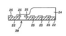
- FIG. 2 ashows a top view 20 of the supporting substrate 22 over the surface of which has been applied a mold cap 24 .
- a polyimide tape 23has been applied over the surface of substrate 22 prior to the formation of the mold cap 24 , copper interconnect traces 25 created over the surface of substrate 22 have been highlighted in FIGS. 2 c and 2 d.
- FIGS. 2 b and 2 cOf special interest to the invention are the surface areas in the four corners of the substrate 22 , of which one illustrative example has been highlighted by surface area 26 in FIG. 2 a.
- FIG. 2 bSpecifically notable in the cross section of FIG. 2 b is the opening 28 that has been created through the substrate 22 , an opening that is provided for each of the corners of substrate 22 of which the cross section shown in FIG. 2 b is a representative example. It is clear that the mold compound 24 will, at the time of filling of the mold cavity with mold 24 , penetrate opening 28 and in so doing will, after hardening of the mold, firmly anchor the mold compound 24 in each of the corners of substrate 22 .
- FIG. 2 cAn example of this is shown in the cross section of FIG. 2 c in which an additional relief or opening 27 is provided for this purpose in the lower part of the mold cavity (the cavity bar). This opening 27 is filled with mold compound at the time that the mold compound enters into the mold cavity.
- This additional relief 27has been shown in the cross section of FIG. 2 c as being of rounded cross section, resembling a segment of a circle.
- any shape or form that further enhances the anchoring of the mold compound to the underlying substratecan be applied for this purpose of anchoring.
- a finned cross sectionresembling for instance cooling fins of a heatsink, wherein parts of the additional relief fan-out as separate sub-elements from a central part can be envisioned as providing extreme anchoring capabilities.
- FIG. 2 dshows a top view of anchor 26 of FIG. 2 a, more clearly highlighting the location of the anchor 26 of mold compound with respect to both the substrate 22 and the applied mold cap 24 .
- the anchor 26extends out (as shown in FIG. 2 b ) parallel to the plane of the substrate 22 from the body of the mold compound over the semiconductor device (the mold cap 24 ) to the opening 28 . This assures that the mold compound of the anchor 26 penetrates perpendicular to the plane of the substrate 22 into the opening 28 created through the substrate 22 .
- FIG. 3 athere is shown a cross section 32 of a top cavity bar, a cross section 30 of a bottom cavity bar, a substrate 34 with copper interconnect traces 35 provided over the surface thereof.
- Anchor opening 37has been provided through (each of the four) corners of substrate 34 , by modifying the contours of the top and bottom cavity bars 32 / 30 where these cavity bars are aligned with the anchor opening 37 , the contours of the applied mold compound can be controlled.
- a top cavity relief 36has been indicated that extends over a distance of substrate 34 , allowing additional mold compound to collect over the surface of the substrate 34 and surrounding the anchor opening 37 .
- a bottom cavity relief 38has the same effects as this effect is now introduced for mold collection underneath the substrate 34 .
- the combined effect of these relief 36 and relief 38is shown in the completed mold compound 38 as shown in the cross section of FIG. 3 b, where the anchor area 33 is now provided with mold compound 38 that extends above the upper and below the lower surface of substrate 34 .
- Copper traces 35are also highlighted in the cross sections of FIGS. 3 a and 3 b.
- FIGS. 3 c and 3 dAn additional implementation that closely resembles the implementation shown in FIGS. 3 a and 3 b is highlighted in FIGS. 3 c and 3 d.
- the relief 38 , FIG. 3 a, in the bottom cavity bar 30 ′is omitted, resulting in a completed mold compound 38 ′ shown in cross section in FIG. 3 d.
- the anchor area 33 ′is now provided with mold compound 38 ′ that extends above the upper surface of substrate 34 .
- FIGS. 4 a and 4 bboth FIGS. 4 a and 4 b showing a top view of one (of the four) corner of substrates 40 and 42 .
- the difference between substrates 40 and 42is created by the difference in the creation of the anchor holes 45 (FIG. 4 a ) and 43 (FIG. 4 b ).
- the anchor hole 45has been created using a drilling or punch-through process, which as shown in the cross section of FIG. 4 b as not differentiating between the presence or absence or copper 41 .
- the anchor hole 43has been created applying an etch process, which creates the anchor through hole 43 while not affecting copper 46 , creating overhang copper 46 .
- Elements 44 , FIG. 4 a,are copper pads created over the surface of substrate 40 , 48 is polyimide tape applied over the surface of substrate 40 .
Landscapes
- Engineering & Computer Science (AREA)
- Microelectronics & Electronic Packaging (AREA)
- Physics & Mathematics (AREA)
- Condensed Matter Physics & Semiconductors (AREA)
- General Physics & Mathematics (AREA)
- Computer Hardware Design (AREA)
- Power Engineering (AREA)
- Manufacturing & Machinery (AREA)
- Encapsulation Of And Coatings For Semiconductor Or Solid State Devices (AREA)
Abstract
Description
Claims (20)
Priority Applications (2)
| Application Number | Priority Date | Filing Date | Title |
|---|---|---|---|
| US10/315,533US6825067B2 (en) | 2002-12-10 | 2002-12-10 | Mold cap anchoring method for molded flex BGA packages |
| US10/914,870US6960493B2 (en) | 2002-12-10 | 2004-08-09 | Semiconductor device package |
Applications Claiming Priority (1)
| Application Number | Priority Date | Filing Date | Title |
|---|---|---|---|
| US10/315,533US6825067B2 (en) | 2002-12-10 | 2002-12-10 | Mold cap anchoring method for molded flex BGA packages |
Related Child Applications (1)
| Application Number | Title | Priority Date | Filing Date |
|---|---|---|---|
| US10/914,870DivisionUS6960493B2 (en) | 2002-12-10 | 2004-08-09 | Semiconductor device package |
Publications (2)
| Publication Number | Publication Date |
|---|---|
| US20040108601A1 US20040108601A1 (en) | 2004-06-10 |
| US6825067B2true US6825067B2 (en) | 2004-11-30 |
Family
ID=32468729
Family Applications (2)
| Application Number | Title | Priority Date | Filing Date |
|---|---|---|---|
| US10/315,533Expired - LifetimeUS6825067B2 (en) | 2002-12-10 | 2002-12-10 | Mold cap anchoring method for molded flex BGA packages |
| US10/914,870Expired - LifetimeUS6960493B2 (en) | 2002-12-10 | 2004-08-09 | Semiconductor device package |
Family Applications After (1)
| Application Number | Title | Priority Date | Filing Date |
|---|---|---|---|
| US10/914,870Expired - LifetimeUS6960493B2 (en) | 2002-12-10 | 2004-08-09 | Semiconductor device package |
Country Status (1)
| Country | Link |
|---|---|
| US (2) | US6825067B2 (en) |
Cited By (15)
| Publication number | Priority date | Publication date | Assignee | Title |
|---|---|---|---|---|
| US20070241423A1 (en)* | 2006-04-14 | 2007-10-18 | Taylor William P | Methods and apparatus for integrated circuit having multiple dies with at least one on chip capacitor |
| US20080034582A1 (en)* | 2006-04-14 | 2008-02-14 | Taylor William P | Methods for sensor having capacitor on chip |
| US20100052424A1 (en)* | 2008-08-26 | 2010-03-04 | Taylor William P | Methods and apparatus for integrated circuit having integrated energy storage device |
| US8093670B2 (en) | 2008-07-24 | 2012-01-10 | Allegro Microsystems, Inc. | Methods and apparatus for integrated circuit having on chip capacitor with eddy current reductions |
| US8629539B2 (en) | 2012-01-16 | 2014-01-14 | Allegro Microsystems, Llc | Methods and apparatus for magnetic sensor having non-conductive die paddle |
| US9030000B2 (en) | 2013-06-14 | 2015-05-12 | Freescale Semiconductor, Inc. | Mold cap for semiconductor device |
| US9228860B2 (en) | 2006-07-14 | 2016-01-05 | Allegro Microsystems, Llc | Sensor and method of providing a sensor |
| US9411025B2 (en) | 2013-04-26 | 2016-08-09 | Allegro Microsystems, Llc | Integrated circuit package having a split lead frame and a magnet |
| US9494660B2 (en) | 2012-03-20 | 2016-11-15 | Allegro Microsystems, Llc | Integrated circuit package having a split lead frame |
| US9666788B2 (en) | 2012-03-20 | 2017-05-30 | Allegro Microsystems, Llc | Integrated circuit package having a split lead frame |
| US9812588B2 (en) | 2012-03-20 | 2017-11-07 | Allegro Microsystems, Llc | Magnetic field sensor integrated circuit with integral ferromagnetic material |
| US10234513B2 (en) | 2012-03-20 | 2019-03-19 | Allegro Microsystems, Llc | Magnetic field sensor integrated circuit with integral ferromagnetic material |
| US10411498B2 (en) | 2015-10-21 | 2019-09-10 | Allegro Microsystems, Llc | Apparatus and methods for extending sensor integrated circuit operation through a power disturbance |
| US10978897B2 (en) | 2018-04-02 | 2021-04-13 | Allegro Microsystems, Llc | Systems and methods for suppressing undesirable voltage supply artifacts |
| US10991644B2 (en) | 2019-08-22 | 2021-04-27 | Allegro Microsystems, Llc | Integrated circuit package having a low profile |
Families Citing this family (2)
| Publication number | Priority date | Publication date | Assignee | Title |
|---|---|---|---|---|
| US20030205828A9 (en)* | 2001-04-05 | 2003-11-06 | Larry Kinsman | Circuit substrates, semiconductor packages, and ball grid arrays |
| US9059187B2 (en)* | 2010-09-30 | 2015-06-16 | Ibiden Co., Ltd. | Electronic component having encapsulated wiring board and method for manufacturing the same |
Citations (9)
| Publication number | Priority date | Publication date | Assignee | Title |
|---|---|---|---|---|
| US5136366A (en)* | 1990-11-05 | 1992-08-04 | Motorola, Inc. | Overmolded semiconductor package with anchoring means |
| US5255157A (en)* | 1992-01-24 | 1993-10-19 | National Semiconductor Corporation | Plastic pin grid array package with locking pillars |
| US5336931A (en)* | 1993-09-03 | 1994-08-09 | Motorola, Inc. | Anchoring method for flow formed integrated circuit covers |
| US5612576A (en)* | 1992-10-13 | 1997-03-18 | Motorola | Self-opening vent hole in an overmolded semiconductor device |
| US5736789A (en)* | 1994-07-26 | 1998-04-07 | Sgs-Thomson Microelectronics S.A. | Ball grid array casing for integrated circuits |
| US5773895A (en)* | 1996-04-03 | 1998-06-30 | Intel Corporation | Anchor provisions to prevent mold delamination in an overmolded plastic array package |
| US5841192A (en)* | 1994-07-21 | 1998-11-24 | Sgs-Thomson Microelectronics S.A. | Injection molded ball grid array casing |
| US5909054A (en)* | 1995-05-16 | 1999-06-01 | Kabushiki Kaisha Toshiba | Semiconductor device having a multiple-terminal integrated circuit formed on a circuit substrate |
| US6214643B1 (en)* | 1998-06-09 | 2001-04-10 | Stmicroelectronics, Inc. | Stress reduction for flip chip package |
- 2002
- 2002-12-10USUS10/315,533patent/US6825067B2/ennot_activeExpired - Lifetime
- 2004
- 2004-08-09USUS10/914,870patent/US6960493B2/ennot_activeExpired - Lifetime
Patent Citations (9)
| Publication number | Priority date | Publication date | Assignee | Title |
|---|---|---|---|---|
| US5136366A (en)* | 1990-11-05 | 1992-08-04 | Motorola, Inc. | Overmolded semiconductor package with anchoring means |
| US5255157A (en)* | 1992-01-24 | 1993-10-19 | National Semiconductor Corporation | Plastic pin grid array package with locking pillars |
| US5612576A (en)* | 1992-10-13 | 1997-03-18 | Motorola | Self-opening vent hole in an overmolded semiconductor device |
| US5336931A (en)* | 1993-09-03 | 1994-08-09 | Motorola, Inc. | Anchoring method for flow formed integrated circuit covers |
| US5841192A (en)* | 1994-07-21 | 1998-11-24 | Sgs-Thomson Microelectronics S.A. | Injection molded ball grid array casing |
| US5736789A (en)* | 1994-07-26 | 1998-04-07 | Sgs-Thomson Microelectronics S.A. | Ball grid array casing for integrated circuits |
| US5909054A (en)* | 1995-05-16 | 1999-06-01 | Kabushiki Kaisha Toshiba | Semiconductor device having a multiple-terminal integrated circuit formed on a circuit substrate |
| US5773895A (en)* | 1996-04-03 | 1998-06-30 | Intel Corporation | Anchor provisions to prevent mold delamination in an overmolded plastic array package |
| US6214643B1 (en)* | 1998-06-09 | 2001-04-10 | Stmicroelectronics, Inc. | Stress reduction for flip chip package |
Cited By (26)
| Publication number | Priority date | Publication date | Assignee | Title |
|---|---|---|---|---|
| US20080034582A1 (en)* | 2006-04-14 | 2008-02-14 | Taylor William P | Methods for sensor having capacitor on chip |
| US7676914B2 (en) | 2006-04-14 | 2010-03-16 | Allegro Microsystems, Inc. | Methods for sensor having capacitor on chip |
| US7687882B2 (en) | 2006-04-14 | 2010-03-30 | Allegro Microsystems, Inc. | Methods and apparatus for integrated circuit having multiple dies with at least one on chip capacitor |
| US20070241423A1 (en)* | 2006-04-14 | 2007-10-18 | Taylor William P | Methods and apparatus for integrated circuit having multiple dies with at least one on chip capacitor |
| US9228860B2 (en) | 2006-07-14 | 2016-01-05 | Allegro Microsystems, Llc | Sensor and method of providing a sensor |
| US8093670B2 (en) | 2008-07-24 | 2012-01-10 | Allegro Microsystems, Inc. | Methods and apparatus for integrated circuit having on chip capacitor with eddy current reductions |
| US20100052424A1 (en)* | 2008-08-26 | 2010-03-04 | Taylor William P | Methods and apparatus for integrated circuit having integrated energy storage device |
| US9620705B2 (en) | 2012-01-16 | 2017-04-11 | Allegro Microsystems, Llc | Methods and apparatus for magnetic sensor having non-conductive die paddle |
| US8629539B2 (en) | 2012-01-16 | 2014-01-14 | Allegro Microsystems, Llc | Methods and apparatus for magnetic sensor having non-conductive die paddle |
| US9299915B2 (en) | 2012-01-16 | 2016-03-29 | Allegro Microsystems, Llc | Methods and apparatus for magnetic sensor having non-conductive die paddle |
| US10333055B2 (en) | 2012-01-16 | 2019-06-25 | Allegro Microsystems, Llc | Methods for magnetic sensor having non-conductive die paddle |
| US10234513B2 (en) | 2012-03-20 | 2019-03-19 | Allegro Microsystems, Llc | Magnetic field sensor integrated circuit with integral ferromagnetic material |
| US11677032B2 (en) | 2012-03-20 | 2023-06-13 | Allegro Microsystems, Llc | Sensor integrated circuit with integrated coil and element in central region of mold material |
| US9666788B2 (en) | 2012-03-20 | 2017-05-30 | Allegro Microsystems, Llc | Integrated circuit package having a split lead frame |
| US9812588B2 (en) | 2012-03-20 | 2017-11-07 | Allegro Microsystems, Llc | Magnetic field sensor integrated circuit with integral ferromagnetic material |
| US10230006B2 (en) | 2012-03-20 | 2019-03-12 | Allegro Microsystems, Llc | Magnetic field sensor integrated circuit with an electromagnetic suppressor |
| US9494660B2 (en) | 2012-03-20 | 2016-11-15 | Allegro Microsystems, Llc | Integrated circuit package having a split lead frame |
| US10916665B2 (en) | 2012-03-20 | 2021-02-09 | Allegro Microsystems, Llc | Magnetic field sensor integrated circuit with an integrated coil |
| US11961920B2 (en) | 2012-03-20 | 2024-04-16 | Allegro Microsystems, Llc | Integrated circuit package with magnet having a channel |
| US11828819B2 (en) | 2012-03-20 | 2023-11-28 | Allegro Microsystems, Llc | Magnetic field sensor integrated circuit with integral ferromagnetic material |
| US11444209B2 (en) | 2012-03-20 | 2022-09-13 | Allegro Microsystems, Llc | Magnetic field sensor integrated circuit with an integrated coil enclosed with a semiconductor die by a mold material |
| US9411025B2 (en) | 2013-04-26 | 2016-08-09 | Allegro Microsystems, Llc | Integrated circuit package having a split lead frame and a magnet |
| US9030000B2 (en) | 2013-06-14 | 2015-05-12 | Freescale Semiconductor, Inc. | Mold cap for semiconductor device |
| US10411498B2 (en) | 2015-10-21 | 2019-09-10 | Allegro Microsystems, Llc | Apparatus and methods for extending sensor integrated circuit operation through a power disturbance |
| US10978897B2 (en) | 2018-04-02 | 2021-04-13 | Allegro Microsystems, Llc | Systems and methods for suppressing undesirable voltage supply artifacts |
| US10991644B2 (en) | 2019-08-22 | 2021-04-27 | Allegro Microsystems, Llc | Integrated circuit package having a low profile |
Also Published As
| Publication number | Publication date |
|---|---|
| US20040108601A1 (en) | 2004-06-10 |
| US20050006668A1 (en) | 2005-01-13 |
| US6960493B2 (en) | 2005-11-01 |
Similar Documents
| Publication | Publication Date | Title |
|---|---|---|
| US6825067B2 (en) | Mold cap anchoring method for molded flex BGA packages | |
| US6918178B2 (en) | Method of attaching a heat sink to an IC package | |
| US6294100B1 (en) | Exposed die leadless plastic chip carrier | |
| US7091581B1 (en) | Integrated circuit package and process for fabricating the same | |
| US7417329B2 (en) | System-in-package structure | |
| US8581375B2 (en) | Leadframe-based mold array package heat spreader and fabrication method therefor | |
| CN114256170B (en) | Fan-out packaging structure and preparation method thereof | |
| US6246124B1 (en) | Encapsulated chip module and method of making same | |
| US9281256B2 (en) | Package encapsulant relief feature | |
| US7309622B2 (en) | Integrated circuit package system with heat sink | |
| JPH06505126A (en) | Carrier ring for semiconductor packages | |
| US7863730B2 (en) | Array-molded package heat spreader and fabrication method therefor | |
| US6400005B1 (en) | Magnetic insert into mold cavity to prevent resin bleeding from bond area of pre-mold (open cavity) plastic chip carrier during molding process | |
| US8610262B1 (en) | Ball grid array package with improved thermal characteristics | |
| US7579680B2 (en) | Packaging system for semiconductor devices | |
| JP2000040676A (en) | Manufacture of semiconductor device | |
| US6160311A (en) | Enhanced heat dissipating chip scale package method and devices | |
| US7691745B1 (en) | Land patterns for a semiconductor stacking structure and method therefor | |
| US20080006933A1 (en) | Heat-dissipating package structure and fabrication method thereof | |
| US11195812B2 (en) | Method for fabricating an encapsulated electronic package using a supporting plate | |
| US20080251910A1 (en) | Fabricating method of semiconductor package and heat-dissipating structure applicable thereto | |
| CN223414071U (en) | Packaging structure | |
| US20050224936A1 (en) | Chip package structure | |
| KR200179419Y1 (en) | Semiconductor package | |
| KR100542671B1 (en) | Semiconductor package and manufacturing method |
Legal Events
| Date | Code | Title | Description |
|---|---|---|---|
| AS | Assignment | Owner name:ST ASSEMBLY TEST SERVICES PTE LTD, SINGAPORE Free format text:ASSIGNMENT OF ASSIGNORS INTEREST;ASSIGNORS:ARARAO, VIRGIL C.;APALE, HERMES T.;SHIM, IL KWON;REEL/FRAME:013572/0799 Effective date:20020911 | |
| STCF | Information on status: patent grant | Free format text:PATENTED CASE | |
| FPAY | Fee payment | Year of fee payment:4 | |
| FPAY | Fee payment | Year of fee payment:8 | |
| AS | Assignment | Owner name:CITICORP INTERNATIONAL LIMITED, AS COMMON SECURITY AGENT, HONG KONG Free format text:SECURITY INTEREST;ASSIGNORS:STATS CHIPPAC, INC.;STATS CHIPPAC LTD.;REEL/FRAME:036288/0748 Effective date:20150806 Owner name:STATS CHIPPAC LTD., SINGAPORE Free format text:CHANGE OF NAME;ASSIGNOR:ST ASSEMBLY TEST SERVICES LTD.;REEL/FRAME:036286/0590 Effective date:20040608 Owner name:CITICORP INTERNATIONAL LIMITED, AS COMMON SECURITY Free format text:SECURITY INTEREST;ASSIGNORS:STATS CHIPPAC, INC.;STATS CHIPPAC LTD.;REEL/FRAME:036288/0748 Effective date:20150806 | |
| AS | Assignment | Owner name:STATS CHIPPAC PTE. LTE., SINGAPORE Free format text:CHANGE OF NAME;ASSIGNOR:STATS CHIPPAC LTD.;REEL/FRAME:038378/0400 Effective date:20160329 | |
| FPAY | Fee payment | Year of fee payment:12 | |
| AS | Assignment | Owner name:STATS CHIPPAC, INC., CALIFORNIA Free format text:RELEASE BY SECURED PARTY;ASSIGNOR:CITICORP INTERNATIONAL LIMITED, AS COMMON SECURITY AGENT;REEL/FRAME:052950/0497 Effective date:20190503 Owner name:STATS CHIPPAC PTE. LTD. FORMERLY KNOWN AS STATS CHIPPAC LTD., SINGAPORE Free format text:RELEASE BY SECURED PARTY;ASSIGNOR:CITICORP INTERNATIONAL LIMITED, AS COMMON SECURITY AGENT;REEL/FRAME:052950/0497 Effective date:20190503 | |
| AS | Assignment | Owner name:STATS CHIPPAC PTE. LTD., DISTRICT OF COLUMBIA Free format text:CORRECTIVE ASSIGNMENT TO CORRECT THE ASSIGNEE'S NAME PREVIOUSLY RECORDED AT REEL: 038378 FRAME: 0400. ASSIGNOR(S) HEREBY CONFIRMS THE ASSIGNMENT;ASSIGNOR:STATS CHIPPAC LTD.;REEL/FRAME:064806/0593 Effective date:20160329 |