US6824857B2 - Circuit elements having an embedded conductive trace and methods of manufacture - Google Patents
Circuit elements having an embedded conductive trace and methods of manufactureDownload PDFInfo
- Publication number
- US6824857B2 US6824857B2US10/113,733US11373302AUS6824857B2US 6824857 B2US6824857 B2US 6824857B2US 11373302 AUS11373302 AUS 11373302AUS 6824857 B2US6824857 B2US 6824857B2
- Authority
- US
- United States
- Prior art keywords
- substrate
- circuit element
- thermoplastic substrate
- conductive
- thermoplastic
- Prior art date
- Legal status (The legal status is an assumption and is not a legal conclusion. Google has not performed a legal analysis and makes no representation as to the accuracy of the status listed.)
- Expired - Fee Related, expires
Links
- 238000000034methodMethods0.000titleabstractdescription61
- 238000004519manufacturing processMethods0.000titledescription5
- 239000000758substrateSubstances0.000claimsabstractdescription259
- 229920001169thermoplasticPolymers0.000claimsabstractdescription163
- 239000004416thermosoftening plasticSubstances0.000claimsabstractdescription157
- 239000002245particleSubstances0.000claimsdescription57
- -1polyethylenePolymers0.000claimsdescription35
- 229920000728polyesterPolymers0.000claimsdescription28
- 238000007747platingMethods0.000claimsdescription27
- 238000009826distributionMethods0.000claimsdescription26
- 239000005038ethylene vinyl acetateSubstances0.000claimsdescription25
- DQXBYHZEEUGOBF-UHFFFAOYSA-Nbut-3-enoic acid;etheneChemical compoundC=C.OC(=O)CC=CDQXBYHZEEUGOBF-UHFFFAOYSA-N0.000claimsdescription23
- 229920001200poly(ethylene-vinyl acetate)Polymers0.000claimsdescription23
- DERLTVRRWCJVCP-UHFFFAOYSA-Nethene;ethyl acetateChemical compoundC=C.CCOC(C)=ODERLTVRRWCJVCP-UHFFFAOYSA-N0.000claimsdescription15
- 239000004698PolyethyleneSubstances0.000claimsdescription14
- VYPSYNLAJGMNEJ-UHFFFAOYSA-NSilicium dioxideChemical compoundO=[Si]=OVYPSYNLAJGMNEJ-UHFFFAOYSA-N0.000claimsdescription14
- 229920000573polyethylenePolymers0.000claimsdescription14
- 229920003207poly(ethylene-2,6-naphthalate)Polymers0.000claimsdescription10
- 239000004642PolyimideSubstances0.000claimsdescription9
- 229920001577copolymerPolymers0.000claimsdescription9
- 229910052751metalInorganic materials0.000claimsdescription9
- 239000002184metalSubstances0.000claimsdescription9
- 229920001721polyimidePolymers0.000claimsdescription9
- 229920000642polymerPolymers0.000claimsdescription9
- 239000004793PolystyreneSubstances0.000claimsdescription8
- 229920000515polycarbonatePolymers0.000claimsdescription8
- 239000004417polycarbonateSubstances0.000claimsdescription8
- 239000011112polyethylene naphthalateSubstances0.000claimsdescription8
- 229920002223polystyrenePolymers0.000claimsdescription8
- 239000000843powderSubstances0.000claimsdescription8
- 239000004734Polyphenylene sulfideSubstances0.000claimsdescription7
- 239000012943hotmeltSubstances0.000claimsdescription7
- 229920000069polyphenylene sulfidePolymers0.000claimsdescription7
- 239000011253protective coatingSubstances0.000claimsdescription7
- 239000000377silicon dioxideSubstances0.000claimsdescription7
- 239000004743PolypropyleneSubstances0.000claimsdescription6
- 239000000463materialSubstances0.000claimsdescription6
- 229920001155polypropylenePolymers0.000claimsdescription6
- 239000011888foilSubstances0.000claimsdescription4
- 239000011521glassSubstances0.000claimsdescription3
- 238000007639printingMethods0.000abstractdescription44
- 238000010438heat treatmentMethods0.000abstractdescription25
- 239000010410layerSubstances0.000description67
- 239000000976inkSubstances0.000description65
- 229910000679solderInorganic materials0.000description22
- 239000002904solventSubstances0.000description21
- 239000000123paperSubstances0.000description16
- 239000004020conductorSubstances0.000description15
- 229920005989resinPolymers0.000description14
- 239000011347resinSubstances0.000description14
- 238000001035dryingMethods0.000description12
- BQCADISMDOOEFD-UHFFFAOYSA-NSilverChemical compound[Ag]BQCADISMDOOEFD-UHFFFAOYSA-N0.000description10
- 230000005855radiationEffects0.000description10
- 229910052709silverInorganic materials0.000description10
- 239000004332silverSubstances0.000description10
- 238000012545processingMethods0.000description9
- 239000003981vehicleSubstances0.000description9
- 238000000576coating methodMethods0.000description8
- 238000004132cross linkingMethods0.000description8
- 238000009713electroplatingMethods0.000description8
- 239000000203mixtureSubstances0.000description8
- 230000008901benefitEffects0.000description7
- 239000011248coating agentSubstances0.000description7
- 238000010894electron beam technologyMethods0.000description7
- 230000006698inductionEffects0.000description7
- 230000008569processEffects0.000description7
- XEKOWRVHYACXOJ-UHFFFAOYSA-NEthyl acetateChemical compoundCCOC(C)=OXEKOWRVHYACXOJ-UHFFFAOYSA-N0.000description6
- RYGMFSIKBFXOCR-UHFFFAOYSA-NCopperChemical compound[Cu]RYGMFSIKBFXOCR-UHFFFAOYSA-N0.000description5
- 150000001338aliphatic hydrocarbonsChemical class0.000description5
- 230000008859changeEffects0.000description5
- 229910052802copperInorganic materials0.000description5
- 239000010949copperSubstances0.000description5
- PXHVJJICTQNCMI-UHFFFAOYSA-NNickelChemical compound[Ni]PXHVJJICTQNCMI-UHFFFAOYSA-N0.000description4
- KDLHZDBZIXYQEI-UHFFFAOYSA-NPalladiumChemical compound[Pd]KDLHZDBZIXYQEI-UHFFFAOYSA-N0.000description4
- 239000003990capacitorSubstances0.000description4
- 230000007423decreaseEffects0.000description4
- 230000003287optical effectEffects0.000description4
- 239000006072pasteSubstances0.000description4
- 239000000126substanceSubstances0.000description4
- 238000012360testing methodMethods0.000description4
- KFZMGEQAYNKOFK-UHFFFAOYSA-NIsopropanolChemical compoundCC(C)OKFZMGEQAYNKOFK-UHFFFAOYSA-N0.000description3
- 239000000853adhesiveSubstances0.000description3
- 230000001070adhesive effectEffects0.000description3
- 229920000180alkydPolymers0.000description3
- 239000003963antioxidant agentSubstances0.000description3
- 150000004945aromatic hydrocarbonsChemical class0.000description3
- 230000002902bimodal effectEffects0.000description3
- 230000005540biological transmissionEffects0.000description3
- 238000007796conventional methodMethods0.000description3
- 238000013461designMethods0.000description3
- 238000005516engineering processMethods0.000description3
- 238000007757hot melt coatingMethods0.000description3
- 239000004615ingredientSubstances0.000description3
- 238000002156mixingMethods0.000description3
- 238000000518rheometryMethods0.000description3
- 230000000930thermomechanical effectEffects0.000description3
- 238000012546transferMethods0.000description3
- 239000000654additiveSubstances0.000description2
- 239000002390adhesive tapeSubstances0.000description2
- 230000003078antioxidant effectEffects0.000description2
- 230000015572biosynthetic processEffects0.000description2
- 239000003795chemical substances by applicationSubstances0.000description2
- 238000004891communicationMethods0.000description2
- 239000002131composite materialSubstances0.000description2
- 238000005530etchingMethods0.000description2
- RRAFCDWBNXTKKO-UHFFFAOYSA-NeugenolChemical compoundCOC1=CC(CC=C)=CC=C1ORRAFCDWBNXTKKO-UHFFFAOYSA-N0.000description2
- 238000001125extrusionMethods0.000description2
- 238000009472formulationMethods0.000description2
- PCHJSUWPFVWCPO-UHFFFAOYSA-NgoldChemical compound[Au]PCHJSUWPFVWCPO-UHFFFAOYSA-N0.000description2
- 229910052737goldInorganic materials0.000description2
- 239000010931goldSubstances0.000description2
- 238000000227grindingMethods0.000description2
- 238000010030laminatingMethods0.000description2
- 238000003475laminationMethods0.000description2
- 238000011031large-scale manufacturing processMethods0.000description2
- 238000012986modificationMethods0.000description2
- 230000004048modificationEffects0.000description2
- 229910052759nickelInorganic materials0.000description2
- 229910052763palladiumInorganic materials0.000description2
- 229920003023plasticPolymers0.000description2
- 239000004033plasticSubstances0.000description2
- BASFCYQUMIYNBI-UHFFFAOYSA-NplatinumChemical compound[Pt]BASFCYQUMIYNBI-UHFFFAOYSA-N0.000description2
- 238000002360preparation methodMethods0.000description2
- 238000010561standard procedureMethods0.000description2
- 238000001757thermogravimetry curveMethods0.000description2
- 235000012431wafersNutrition0.000description2
- RNFJDJUURJAICM-UHFFFAOYSA-N2,2,4,4,6,6-hexaphenoxy-1,3,5-triaza-2$l^{5},4$l^{5},6$l^{5}-triphosphacyclohexa-1,3,5-trieneChemical compoundN=1P(OC=2C=CC=CC=2)(OC=2C=CC=CC=2)=NP(OC=2C=CC=CC=2)(OC=2C=CC=CC=2)=NP=1(OC=1C=CC=CC=1)OC1=CC=CC=C1RNFJDJUURJAICM-UHFFFAOYSA-N0.000description1
- OKTJSMMVPCPJKN-UHFFFAOYSA-NCarbonChemical compound[C]OKTJSMMVPCPJKN-UHFFFAOYSA-N0.000description1
- 239000004215Carbon black (E152)Substances0.000description1
- NPBVQXIMTZKSBA-UHFFFAOYSA-NChavibetolNatural productsCOC1=CC=C(CC=C)C=C1ONPBVQXIMTZKSBA-UHFFFAOYSA-N0.000description1
- LFQSCWFLJHTTHZ-UHFFFAOYSA-NEthanolChemical compoundCCOLFQSCWFLJHTTHZ-UHFFFAOYSA-N0.000description1
- 239000005770EugenolSubstances0.000description1
- 206010034133Pathogen resistanceDiseases0.000description1
- UVMRYBDEERADNV-UHFFFAOYSA-NPseudoeugenolNatural productsCOC1=CC(C(C)=C)=CC=C1OUVMRYBDEERADNV-UHFFFAOYSA-N0.000description1
- 239000003513alkaliSubstances0.000description1
- 238000004458analytical methodMethods0.000description1
- 238000013459approachMethods0.000description1
- 230000004888barrier functionEffects0.000description1
- 229910052799carbonInorganic materials0.000description1
- 239000004927claySubstances0.000description1
- 239000010634clove oilSubstances0.000description1
- 230000001010compromised effectEffects0.000description1
- 230000001268conjugating effectEffects0.000description1
- 230000021615conjugationEffects0.000description1
- 238000010924continuous productionMethods0.000description1
- 238000004320controlled atmosphereMethods0.000description1
- 238000001816coolingMethods0.000description1
- 230000007797corrosionEffects0.000description1
- 238000005260corrosionMethods0.000description1
- 238000007766curtain coatingMethods0.000description1
- 238000000151depositionMethods0.000description1
- 230000008021depositionEffects0.000description1
- 239000002274desiccantSubstances0.000description1
- 235000014113dietary fatty acidsNutrition0.000description1
- 239000006185dispersionSubstances0.000description1
- 238000005553drillingMethods0.000description1
- 238000004070electrodepositionMethods0.000description1
- 238000007772electroless platingMethods0.000description1
- 238000001227electron beam curingMethods0.000description1
- 230000007613environmental effectEffects0.000description1
- 239000003822epoxy resinSubstances0.000description1
- 229960002217eugenolDrugs0.000description1
- 239000000194fatty acidSubstances0.000description1
- 229930195729fatty acidNatural products0.000description1
- 150000004665fatty acidsChemical class0.000description1
- 239000000835fiberSubstances0.000description1
- 239000003063flame retardantSubstances0.000description1
- 239000003365glass fiberSubstances0.000description1
- LNEPOXFFQSENCJ-UHFFFAOYSA-NhaloperidolChemical compoundC1CC(O)(C=2C=CC(Cl)=CC=2)CCN1CCCC(=O)C1=CC=C(F)C=C1LNEPOXFFQSENCJ-UHFFFAOYSA-N0.000description1
- 238000009474hot melt extrusionMethods0.000description1
- 229930195733hydrocarbonNatural products0.000description1
- 150000002430hydrocarbonsChemical class0.000description1
- 239000003999initiatorSubstances0.000description1
- 238000007689inspectionMethods0.000description1
- 238000007644letterpress printingMethods0.000description1
- 230000000670limiting effectEffects0.000description1
- 235000021388linseed oilNutrition0.000description1
- 239000000944linseed oilSubstances0.000description1
- 238000001459lithographyMethods0.000description1
- 230000000873masking effectEffects0.000description1
- 238000002844meltingMethods0.000description1
- 230000008018meltingEffects0.000description1
- 230000003278mimic effectEffects0.000description1
- 239000012454non-polar solventSubstances0.000description1
- 230000036961partial effectEffects0.000description1
- 238000000206photolithographyMethods0.000description1
- 229920002120photoresistant polymerPolymers0.000description1
- 239000000049pigmentSubstances0.000description1
- 229910052697platinumInorganic materials0.000description1
- 229920003223poly(pyromellitimide-1,4-diphenyl ether)Polymers0.000description1
- 229920000647polyepoxidePolymers0.000description1
- 229920002959polymer blendPolymers0.000description1
- 229920006254polymer filmPolymers0.000description1
- 239000000523sampleSubstances0.000description1
- 238000007650screen-printingMethods0.000description1
- 239000002356single layerSubstances0.000description1
- 239000002002slurrySubstances0.000description1
- 238000007614solvationMethods0.000description1
- 238000000935solvent evaporationMethods0.000description1
- ZSDSQXJSNMTJDA-UHFFFAOYSA-NtrifluralinChemical compoundCCCN(CCC)C1=C([N+]([O-])=O)C=C(C(F)(F)F)C=C1[N+]([O-])=OZSDSQXJSNMTJDA-UHFFFAOYSA-N0.000description1
- XLYOFNOQVPJJNP-UHFFFAOYSA-NwaterSubstancesOXLYOFNOQVPJJNP-UHFFFAOYSA-N0.000description1
Images


Classifications
- H—ELECTRICITY
- H05—ELECTRIC TECHNIQUES NOT OTHERWISE PROVIDED FOR
- H05K—PRINTED CIRCUITS; CASINGS OR CONSTRUCTIONAL DETAILS OF ELECTRIC APPARATUS; MANUFACTURE OF ASSEMBLAGES OF ELECTRICAL COMPONENTS
- H05K3/00—Apparatus or processes for manufacturing printed circuits
- H05K3/22—Secondary treatment of printed circuits
- H05K3/24—Reinforcing the conductive pattern
- H05K3/245—Reinforcing conductive patterns made by printing techniques or by other techniques for applying conductive pastes, inks or powders; Reinforcing other conductive patterns by such techniques
- H05K3/246—Reinforcing conductive paste, ink or powder patterns by other methods, e.g. by plating
- G—PHYSICS
- G08—SIGNALLING
- G08B—SIGNALLING OR CALLING SYSTEMS; ORDER TELEGRAPHS; ALARM SYSTEMS
- G08B13/00—Burglar, theft or intruder alarms
- G08B13/22—Electrical actuation
- G08B13/24—Electrical actuation by interference with electromagnetic field distribution
- G08B13/2402—Electronic Article Surveillance [EAS], i.e. systems using tags for detecting removal of a tagged item from a secure area, e.g. tags for detecting shoplifting
- G08B13/2428—Tag details
- G08B13/2437—Tag layered structure, processes for making layered tags
- G08B13/244—Tag manufacturing, e.g. continuous manufacturing processes
- H—ELECTRICITY
- H05—ELECTRIC TECHNIQUES NOT OTHERWISE PROVIDED FOR
- H05K—PRINTED CIRCUITS; CASINGS OR CONSTRUCTIONAL DETAILS OF ELECTRIC APPARATUS; MANUFACTURE OF ASSEMBLAGES OF ELECTRICAL COMPONENTS
- H05K1/00—Printed circuits
- H05K1/02—Details
- H05K1/03—Use of materials for the substrate
- H05K1/0313—Organic insulating material
- H05K1/0353—Organic insulating material consisting of two or more materials, e.g. two or more polymers, polymer + filler, + reinforcement
- H05K1/036—Multilayers with layers of different types
- H—ELECTRICITY
- H05—ELECTRIC TECHNIQUES NOT OTHERWISE PROVIDED FOR
- H05K—PRINTED CIRCUITS; CASINGS OR CONSTRUCTIONAL DETAILS OF ELECTRIC APPARATUS; MANUFACTURE OF ASSEMBLAGES OF ELECTRICAL COMPONENTS
- H05K3/00—Apparatus or processes for manufacturing printed circuits
- H05K3/10—Apparatus or processes for manufacturing printed circuits in which conductive material is applied to the insulating support in such a manner as to form the desired conductive pattern
- H05K3/12—Apparatus or processes for manufacturing printed circuits in which conductive material is applied to the insulating support in such a manner as to form the desired conductive pattern using thick film techniques, e.g. printing techniques to apply the conductive material or similar techniques for applying conductive paste or ink patterns
- H05K3/1258—Apparatus or processes for manufacturing printed circuits in which conductive material is applied to the insulating support in such a manner as to form the desired conductive pattern using thick film techniques, e.g. printing techniques to apply the conductive material or similar techniques for applying conductive paste or ink patterns by using a substrate provided with a shape pattern, e.g. grooves, banks, resist pattern
- H—ELECTRICITY
- H05—ELECTRIC TECHNIQUES NOT OTHERWISE PROVIDED FOR
- H05K—PRINTED CIRCUITS; CASINGS OR CONSTRUCTIONAL DETAILS OF ELECTRIC APPARATUS; MANUFACTURE OF ASSEMBLAGES OF ELECTRICAL COMPONENTS
- H05K3/00—Apparatus or processes for manufacturing printed circuits
- H05K3/38—Improvement of the adhesion between the insulating substrate and the metal
- H—ELECTRICITY
- H01—ELECTRIC ELEMENTS
- H01F—MAGNETS; INDUCTANCES; TRANSFORMERS; SELECTION OF MATERIALS FOR THEIR MAGNETIC PROPERTIES
- H01F17/00—Fixed inductances of the signal type
- H01F17/0006—Printed inductances
- H01F2017/006—Printed inductances flexible printed inductors
- H—ELECTRICITY
- H01—ELECTRIC ELEMENTS
- H01F—MAGNETS; INDUCTANCES; TRANSFORMERS; SELECTION OF MATERIALS FOR THEIR MAGNETIC PROPERTIES
- H01F41/00—Apparatus or processes specially adapted for manufacturing or assembling magnets, inductances or transformers; Apparatus or processes specially adapted for manufacturing materials characterised by their magnetic properties
- H01F41/02—Apparatus or processes specially adapted for manufacturing or assembling magnets, inductances or transformers; Apparatus or processes specially adapted for manufacturing materials characterised by their magnetic properties for manufacturing cores, coils, or magnets
- H01F41/04—Apparatus or processes specially adapted for manufacturing or assembling magnets, inductances or transformers; Apparatus or processes specially adapted for manufacturing materials characterised by their magnetic properties for manufacturing cores, coils, or magnets for manufacturing coils
- H01F41/041—Printed circuit coils
- H—ELECTRICITY
- H01—ELECTRIC ELEMENTS
- H01F—MAGNETS; INDUCTANCES; TRANSFORMERS; SELECTION OF MATERIALS FOR THEIR MAGNETIC PROPERTIES
- H01F5/00—Coils
- H01F5/003—Printed circuit coils
- H—ELECTRICITY
- H05—ELECTRIC TECHNIQUES NOT OTHERWISE PROVIDED FOR
- H05K—PRINTED CIRCUITS; CASINGS OR CONSTRUCTIONAL DETAILS OF ELECTRIC APPARATUS; MANUFACTURE OF ASSEMBLAGES OF ELECTRICAL COMPONENTS
- H05K1/00—Printed circuits
- H05K1/02—Details
- H05K1/09—Use of materials for the conductive, e.g. metallic pattern
- H05K1/092—Dispersed materials, e.g. conductive pastes or inks
- H05K1/095—Dispersed materials, e.g. conductive pastes or inks for polymer thick films, i.e. having a permanent organic polymeric binder
- H—ELECTRICITY
- H05—ELECTRIC TECHNIQUES NOT OTHERWISE PROVIDED FOR
- H05K—PRINTED CIRCUITS; CASINGS OR CONSTRUCTIONAL DETAILS OF ELECTRIC APPARATUS; MANUFACTURE OF ASSEMBLAGES OF ELECTRICAL COMPONENTS
- H05K2201/00—Indexing scheme relating to printed circuits covered by H05K1/00
- H05K2201/01—Dielectrics
- H05K2201/0104—Properties and characteristics in general
- H05K2201/0129—Thermoplastic polymer, e.g. auto-adhesive layer; Shaping of thermoplastic polymer
- H—ELECTRICITY
- H05—ELECTRIC TECHNIQUES NOT OTHERWISE PROVIDED FOR
- H05K—PRINTED CIRCUITS; CASINGS OR CONSTRUCTIONAL DETAILS OF ELECTRIC APPARATUS; MANUFACTURE OF ASSEMBLAGES OF ELECTRICAL COMPONENTS
- H05K2201/00—Indexing scheme relating to printed circuits covered by H05K1/00
- H05K2201/03—Conductive materials
- H05K2201/0332—Structure of the conductor
- H05K2201/0335—Layered conductors or foils
- H05K2201/0347—Overplating, e.g. for reinforcing conductors or bumps; Plating over filled vias
- H—ELECTRICITY
- H05—ELECTRIC TECHNIQUES NOT OTHERWISE PROVIDED FOR
- H05K—PRINTED CIRCUITS; CASINGS OR CONSTRUCTIONAL DETAILS OF ELECTRIC APPARATUS; MANUFACTURE OF ASSEMBLAGES OF ELECTRICAL COMPONENTS
- H05K2203/00—Indexing scheme relating to apparatus or processes for manufacturing printed circuits covered by H05K3/00
- H05K2203/02—Details related to mechanical or acoustic processing, e.g. drilling, punching, cutting, using ultrasound
- H05K2203/0278—Flat pressure, e.g. for connecting terminals with anisotropic conductive adhesive
- H—ELECTRICITY
- H05—ELECTRIC TECHNIQUES NOT OTHERWISE PROVIDED FOR
- H05K—PRINTED CIRCUITS; CASINGS OR CONSTRUCTIONAL DETAILS OF ELECTRIC APPARATUS; MANUFACTURE OF ASSEMBLAGES OF ELECTRICAL COMPONENTS
- H05K2203/00—Indexing scheme relating to apparatus or processes for manufacturing printed circuits covered by H05K3/00
- H05K2203/10—Using electric, magnetic and electromagnetic fields; Using laser light
- H05K2203/107—Using laser light
- H—ELECTRICITY
- H05—ELECTRIC TECHNIQUES NOT OTHERWISE PROVIDED FOR
- H05K—PRINTED CIRCUITS; CASINGS OR CONSTRUCTIONAL DETAILS OF ELECTRIC APPARATUS; MANUFACTURE OF ASSEMBLAGES OF ELECTRICAL COMPONENTS
- H05K2203/00—Indexing scheme relating to apparatus or processes for manufacturing printed circuits covered by H05K3/00
- H05K2203/11—Treatments characterised by their effect, e.g. heating, cooling, roughening
- H05K2203/1105—Heating or thermal processing not related to soldering, firing, curing or laminating, e.g. for shaping the substrate or during finish plating
- H—ELECTRICITY
- H05—ELECTRIC TECHNIQUES NOT OTHERWISE PROVIDED FOR
- H05K—PRINTED CIRCUITS; CASINGS OR CONSTRUCTIONAL DETAILS OF ELECTRIC APPARATUS; MANUFACTURE OF ASSEMBLAGES OF ELECTRICAL COMPONENTS
- H05K3/00—Apparatus or processes for manufacturing printed circuits
- H05K3/10—Apparatus or processes for manufacturing printed circuits in which conductive material is applied to the insulating support in such a manner as to form the desired conductive pattern
- H05K3/107—Apparatus or processes for manufacturing printed circuits in which conductive material is applied to the insulating support in such a manner as to form the desired conductive pattern by filling grooves in the support with conductive material
- H—ELECTRICITY
- H05—ELECTRIC TECHNIQUES NOT OTHERWISE PROVIDED FOR
- H05K—PRINTED CIRCUITS; CASINGS OR CONSTRUCTIONAL DETAILS OF ELECTRIC APPARATUS; MANUFACTURE OF ASSEMBLAGES OF ELECTRICAL COMPONENTS
- H05K3/00—Apparatus or processes for manufacturing printed circuits
- H05K3/22—Secondary treatment of printed circuits
- H05K3/24—Reinforcing the conductive pattern
- H05K3/245—Reinforcing conductive patterns made by printing techniques or by other techniques for applying conductive pastes, inks or powders; Reinforcing other conductive patterns by such techniques
- Y—GENERAL TAGGING OF NEW TECHNOLOGICAL DEVELOPMENTS; GENERAL TAGGING OF CROSS-SECTIONAL TECHNOLOGIES SPANNING OVER SEVERAL SECTIONS OF THE IPC; TECHNICAL SUBJECTS COVERED BY FORMER USPC CROSS-REFERENCE ART COLLECTIONS [XRACs] AND DIGESTS
- Y10—TECHNICAL SUBJECTS COVERED BY FORMER USPC
- Y10S—TECHNICAL SUBJECTS COVERED BY FORMER USPC CROSS-REFERENCE ART COLLECTIONS [XRACs] AND DIGESTS
- Y10S428/00—Stock material or miscellaneous articles
- Y10S428/901—Printed circuit
- Y—GENERAL TAGGING OF NEW TECHNOLOGICAL DEVELOPMENTS; GENERAL TAGGING OF CROSS-SECTIONAL TECHNOLOGIES SPANNING OVER SEVERAL SECTIONS OF THE IPC; TECHNICAL SUBJECTS COVERED BY FORMER USPC CROSS-REFERENCE ART COLLECTIONS [XRACs] AND DIGESTS
- Y10—TECHNICAL SUBJECTS COVERED BY FORMER USPC
- Y10T—TECHNICAL SUBJECTS COVERED BY FORMER US CLASSIFICATION
- Y10T428/00—Stock material or miscellaneous articles
- Y10T428/24—Structurally defined web or sheet [e.g., overall dimension, etc.]
- Y10T428/24802—Discontinuous or differential coating, impregnation or bond [e.g., artwork, printing, retouched photograph, etc.]
- Y10T428/24917—Discontinuous or differential coating, impregnation or bond [e.g., artwork, printing, retouched photograph, etc.] including metal layer
- Y—GENERAL TAGGING OF NEW TECHNOLOGICAL DEVELOPMENTS; GENERAL TAGGING OF CROSS-SECTIONAL TECHNOLOGIES SPANNING OVER SEVERAL SECTIONS OF THE IPC; TECHNICAL SUBJECTS COVERED BY FORMER USPC CROSS-REFERENCE ART COLLECTIONS [XRACs] AND DIGESTS
- Y10—TECHNICAL SUBJECTS COVERED BY FORMER USPC
- Y10T—TECHNICAL SUBJECTS COVERED BY FORMER US CLASSIFICATION
- Y10T428/00—Stock material or miscellaneous articles
- Y10T428/29—Coated or structually defined flake, particle, cell, strand, strand portion, rod, filament, macroscopic fiber or mass thereof
- Y10T428/2982—Particulate matter [e.g., sphere, flake, etc.]
- Y—GENERAL TAGGING OF NEW TECHNOLOGICAL DEVELOPMENTS; GENERAL TAGGING OF CROSS-SECTIONAL TECHNOLOGIES SPANNING OVER SEVERAL SECTIONS OF THE IPC; TECHNICAL SUBJECTS COVERED BY FORMER USPC CROSS-REFERENCE ART COLLECTIONS [XRACs] AND DIGESTS
- Y10—TECHNICAL SUBJECTS COVERED BY FORMER USPC
- Y10T—TECHNICAL SUBJECTS COVERED BY FORMER US CLASSIFICATION
- Y10T428/00—Stock material or miscellaneous articles
- Y10T428/31504—Composite [nonstructural laminate]
- Y10T428/31551—Of polyamidoester [polyurethane, polyisocyanate, polycarbamate, etc.]
- Y10T428/31645—Next to addition polymer from unsaturated monomers
- Y—GENERAL TAGGING OF NEW TECHNOLOGICAL DEVELOPMENTS; GENERAL TAGGING OF CROSS-SECTIONAL TECHNOLOGIES SPANNING OVER SEVERAL SECTIONS OF THE IPC; TECHNICAL SUBJECTS COVERED BY FORMER USPC CROSS-REFERENCE ART COLLECTIONS [XRACs] AND DIGESTS
- Y10—TECHNICAL SUBJECTS COVERED BY FORMER USPC
- Y10T—TECHNICAL SUBJECTS COVERED BY FORMER US CLASSIFICATION
- Y10T428/00—Stock material or miscellaneous articles
- Y10T428/31504—Composite [nonstructural laminate]
- Y10T428/31721—Of polyimide
- Y—GENERAL TAGGING OF NEW TECHNOLOGICAL DEVELOPMENTS; GENERAL TAGGING OF CROSS-SECTIONAL TECHNOLOGIES SPANNING OVER SEVERAL SECTIONS OF THE IPC; TECHNICAL SUBJECTS COVERED BY FORMER USPC CROSS-REFERENCE ART COLLECTIONS [XRACs] AND DIGESTS
- Y10—TECHNICAL SUBJECTS COVERED BY FORMER USPC
- Y10T—TECHNICAL SUBJECTS COVERED BY FORMER US CLASSIFICATION
- Y10T428/00—Stock material or miscellaneous articles
- Y10T428/31504—Composite [nonstructural laminate]
- Y10T428/31786—Of polyester [e.g., alkyd, etc.]
- Y—GENERAL TAGGING OF NEW TECHNOLOGICAL DEVELOPMENTS; GENERAL TAGGING OF CROSS-SECTIONAL TECHNOLOGIES SPANNING OVER SEVERAL SECTIONS OF THE IPC; TECHNICAL SUBJECTS COVERED BY FORMER USPC CROSS-REFERENCE ART COLLECTIONS [XRACs] AND DIGESTS
- Y10—TECHNICAL SUBJECTS COVERED BY FORMER USPC
- Y10T—TECHNICAL SUBJECTS COVERED BY FORMER US CLASSIFICATION
- Y10T428/00—Stock material or miscellaneous articles
- Y10T428/31504—Composite [nonstructural laminate]
- Y10T428/31855—Of addition polymer from unsaturated monomers
- Y10T428/31909—Next to second addition polymer from unsaturated monomers
- Y10T428/31928—Ester, halide or nitrile of addition polymer
- Y—GENERAL TAGGING OF NEW TECHNOLOGICAL DEVELOPMENTS; GENERAL TAGGING OF CROSS-SECTIONAL TECHNOLOGIES SPANNING OVER SEVERAL SECTIONS OF THE IPC; TECHNICAL SUBJECTS COVERED BY FORMER USPC CROSS-REFERENCE ART COLLECTIONS [XRACs] AND DIGESTS
- Y10—TECHNICAL SUBJECTS COVERED BY FORMER USPC
- Y10T—TECHNICAL SUBJECTS COVERED BY FORMER US CLASSIFICATION
- Y10T428/00—Stock material or miscellaneous articles
- Y10T428/31504—Composite [nonstructural laminate]
- Y10T428/31855—Of addition polymer from unsaturated monomers
- Y10T428/31931—Polyene monomer-containing
- Y—GENERAL TAGGING OF NEW TECHNOLOGICAL DEVELOPMENTS; GENERAL TAGGING OF CROSS-SECTIONAL TECHNOLOGIES SPANNING OVER SEVERAL SECTIONS OF THE IPC; TECHNICAL SUBJECTS COVERED BY FORMER USPC CROSS-REFERENCE ART COLLECTIONS [XRACs] AND DIGESTS
- Y10—TECHNICAL SUBJECTS COVERED BY FORMER USPC
- Y10T—TECHNICAL SUBJECTS COVERED BY FORMER US CLASSIFICATION
- Y10T428/00—Stock material or miscellaneous articles
- Y10T428/31504—Composite [nonstructural laminate]
- Y10T428/31855—Of addition polymer from unsaturated monomers
- Y10T428/31935—Ester, halide or nitrile of addition polymer
Definitions
- the present inventionrelates generally to circuit elements, and more specifically, to methods and apparatus for forming a circuit element including one or more conductive traces at least partially embedded in a thermoplastic substrate.
- Conductive tracestypically are applied to a substrate, such as a silica wafer, using photolithography techniques that require many steps, including application of resist, masking and etching. These steps often use chemicals that are environmentally unfriendly.
- Conductive traces printed on substrates using printing pressestypically are unstable and detach from the substrate when exposed to further processing, e.g., plating baths and solder reflow.
- the conductive tracesalso are typically not capable of being electroplated as they lack sufficient conductivity and first must be electrolessly plated, which is expensive as it requires two plating steps and is environmentally unfriendly.
- the present inventionaddresses these needs and provides additional benefits and improvements.
- the inventionfeatures a circuit element that includes a thermoplastic substrate, and a conductive trace at least partially embedded in the thermoplastic substrate.
- the thermoplastic substratecan be formed from thermoplastic polymers which include ethylene vinyl acetate, ethylene ethyl acetate, polyethylene, polypropylene, polycarbonate, polyimide, polyethylene naphthalate, polyphenylene sulfide, polyester, synthetic paper, polystyrene, and copolymers and combinations thereof.
- the circuit elementcan further include a second substrate, wherein the second substrate is disposed adjacent to the thermoplastic substrate and opposite the conductive trace.
- the thermoplastic substratecan be hot melt coated, co-extruded or laminated onto the second substrate.
- the second substratecan be a second thermoplastic substrate having a second softening temperature that is higher than the softening temperature of the thermoplastic substrate.
- the thermoplastic substratecan be formed from ethylene vinyl acetate, ethylene ethyl acetate, polyethylene, polypropylene, polycarbonate, copolymers or combinations thereof, and the second substrate can be formed from polyimide, polyethylene naphthalate, polyphenylene sulfide, polyester, synthetic paper, polystyrene, or copolymers thereof.
- the second substratealso can be formed from metal, metal foils, paper, glass, silica, and combinations thereof.
- the circuit elementcan further include a third substrate disposed adjacent to the second substrate opposite the thermoplastic substrate.
- the third substratecan be a thermoplastic substrate.
- a conductive tracecan be at least partially embedded in the third thermoplastic substrate.
- the conductive tracecan include conductive particles having a particle size distribution having at least two modes.
- the conductive particlescan include both conductive powder and conductive flakes.
- the conductive flakestypically have a mean aspect ratio between about 2 and about 50.
- the conductive tracecan include conjugated conductive particles.
- the circuit elementcan include electrolytic conductive plating disposed on the conductive trace and/or a protective coating disposed on a surface of the circuit element.
- the inventionfeatures a method of forming a circuit element.
- the methodincludes the steps of providing a thermoplastic substrate having a softening temperature (T S ), printing a conductive ink onto the thermoplastic substrate to form a trace, and embedding the trace into the thermoplastic substrate by heating the thermoplastic substrate to a temperature above about the T S about the trace.
- T Ssoftening temperature
- the methodcan include drying the conductive ink at a temperature less than about the T S to form a trace prior to embedding it into the thermoplastic substrate.
- the methodalso can include using a thermoplastic substrate that also includes one or more additional substrates disposed adjacent to the thermoplastic substrate.
- the methodcan include pre-heating the thermoplastic substrate to a temperature above about the T S , and allowing the thermoplastic substrate to cool to below about the T S , prior to printing the conductive ink onto the thermoplastic substrate.
- the step of embedding the conductive trace into the thermoplastic substratecan be achieved by localized heating.
- the conductive tracecan be embedded into the thermoplastic substrate by induction heating the conductive material in the conductive ink.
- the methodalso can include flashing off at least a portion of a vehicle of the conductive trace and/or conjugating at least a portion of a conductive material in the conductive trace.
- the methodcan include cross-linking the thermoplastic substrate after embedding the conductive trace in the thermoplastic substrate.
- the thermoplastic substratecan be cross-linked by electron beam radiation.
- the methodalso can include printing solder onto the thermoplastic substrate, adding electrical components to the thermoplastic substrate, and heating the solder to a reflow temperature.
- the methodcan include electrolytically plating the conductive trace to form electrolytic conductive plating on the conductive trace and/or coating a surface of the circuit element with a protective coating.
- FIGS. 1 and 2are graphical representations of dimension change versus temperature for ethylene vinyl acetate and ethylene ethyl acetate, respectively;
- FIGS. 3A and 3Bare a plan view and a cross-sectional side view taken along line B—B, respectively, of an exemplary circuit element formed in accordance with the present invention
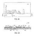
- FIGS. 4A and 4Bare a plan view and a cross-sectional side view taken along line B—B, respectively, of another exemplary circuit element formed in accordance with the present invention.
- FIG. 5is a schematic representation of an exemplary method of forming a circuit element of the present invention.
- FIG. 6is another schematic representation of another exemplary method of forming a circuit element of the present invention.
- circuit elementsthat include at least one conductive trace and methods of their manufacture.
- One aspect of the present inventionis directed to a circuit element including a thermoplastic substrate and a conductive trace at least partially embedded in the thermoplastic substrate.
- thermoplastic substrateis a substrate that becomes plastic, i.e., it becomes viscous or flows, when exposed to thermal energy.
- the softening temperature (Ts) of a thermoplastic layeris the temperature at which the thermoplastic substrate becomes plastic or softens.
- the softening temperatureoften can be qualitatively determined by routine optical inspection of the thermoplastic substrate at different temperatures.
- the softening temperatureis the temperature at which the thermoplastic substrate changes from an opaque or cloudy layer to a translucent layer.
- An alternative method of determining softening temperatureis to dispose a plurality of thermoplastic substrates adjacent to paper layers and send each through a laminator set at increasingly higher temperatures. At about the softening temperature, the thermoplastic substrate will adhere to the paper.
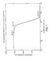
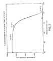
- thermogramis a thermomechanical analysis of a substance that measures the deformation or dimension change of the substance as a function of temperature in a controlled atmosphere. The point at which the dimension change precipitously drops is the softening temperature. Examples of the results of such a test run on a Dupont MTA Thermomechanical (TMA) Analyzer by Chemir/Polytech Laboratories, Inc. (Maryland Heights, Mo.), are depicted in FIGS. 1 and 2.
- FIGS. 1 and 2are graphical representations of dimension change versus temperature for ethylene vinyl acetate and ethylene ethyl acetate, respectively, from about 25° C.
- FIGS. 1 and 2show the dimension change in micrometers from 70° C. to 120° C.
- FIG. 1shows that the ethylene vinyl acetate began to deform at about 88° C., was substantially melted at about 105° C., and has a softening temperature of about 96° C.
- FIG. 2shows that the ethylene ethyl acetate began to deform at about 86° C., was substantially melted at about 111° C., and has a softening temperature of about 98° C.
- a conductive traceis any conductive path.
- Conductive tracesinclude, but are not limited to, circuit board traces, touch pad elements, RFID tags, and printed resistors and capacitors.
- the conductive traces of the present inventioncan be conductive enough to carry current or they can be sufficiently conductive to carry or transmit a signal, such as for use as a touch pad element.
- the conductive traces of the present inventioncan be sufficiently conductive to facilitate electrolytic plating, if additional conductivity is desired.
- the conductive tracesare embedded in the thermoplastic layer such that they interrupt or breach the surface of the thermoplastic layer versus merely being disposed on the surface of the thermoplastic layer. Thus, the conductive traces become an integral part of the circuit element.
- embeddedor “embedding” are used, these terms mean “at least partially embedded” or “at least partially embedding,” respectively, if not otherwise indicated. This is accomplished at least in part by heating the thermoplastic layer to above about its softening temperature at least around the trace.
- the thermoplastic layercan be heated locally, e.g., with induction heating.
- the thermoplastic substratecan be heated globally, e.g., with an oven.
- FIGS. 3A and 3Bare a plan view and a cross-sectional side view taken along line B—B, respectively, of an exemplary circuit element formed in accordance with the present invention.
- the circuit element 100includes a thermoplastic substrate 110 , a second substrate 130 , and a conductive trace 120 at least partially embedded in the thermoplastic substrate 110 .
- an RFID tagis depicted, however, any conductive trace design can printed.
- the thermoplastic substrate, the second substrate and any additional substratescan include any substrate layer that can be used to construct a circuit element.
- the substrate layerscan be provided as individual sheets so that they can be used in a sheet fed process, or as continuous sheets so that they can be processed in a reel to reel or roll to roll process.
- the substrate layersalso can be provided as individual sheets adhered to a continuous film, e.g., by adhesion, co-extrusion or lamination, for processing in a continuous fashion in a commercial printer.
- the substrate layerscan be of any thickness.
- the substrate layersare together thin and flexible enough to be printed in a commercial printer and otherwise processed in a continuous fashion.
- the substrate layerscan be affixed together by various methods known in the art, including, but not limited to, use of adhesives, coating including bar coating and hot melt coating, hot melt extrusion, laminating including heat laminating, and co-extrusion.
- the substrate layersare co-extruded.
- Further substrate layerscan include additional thermoplastic substrate layers that also can include conductive traces partially embedded therein, e.g., to provide a double-sided circuit board.
- Further substrate layersadditionally or alternatively can include internal layers, e.g., dielectric layers such as conventional silica wafers, coated, printed, or laminated on both sides with a conductive material to provide desired mechanical or electrical properties.
- the substrate layers and/or multiple circuit elements of the present inventioncan be combined, e.g., to form a multi-layer circuit board.
- the substrate layerscan include a composite such as glass fiber or paper impregnated with epoxy resins.
- the substrate layersalso can include other additives, e.g., to improve fire retardancy, mechanical strength, thermal strength, and/or dielectric properties.
- the thermoplastic substratecan be formed from any thermoplastic including, but not limited to, polyester, polyimide, polyethylene naphthalate, polyphenylene sulfide, synthetic papers, polyethylene, polypropylene, polycarbonate, ethylene vinyl acetate, ethylene ethyl acetate, and copolymers and combinations of these polymers.
- the thermoplastic substratecan include other materials to increase mechanical strength, to adjust dielectric properties, and/or to render the substrate flame retardant.
- the substrate layersreadily can be chosen by the skilled practitioner depending on the properties desired for the circuit element.
- a second substrate formed from polyimide or polyethylene naphthalatecan be employed that is coated with a thermoplastic substrate having a lower T S .
- a second substrate that is a metal or a metal foilcan be employed.
- a preferred thermoplastic polymeris ethylene vinyl acetate.
- Another preferred thermoplastic polymeris ethylene ethyl acetate.
- Suitable two-layer substratesinclude polyester substrates hot melt coated with ethylene vinyl acetate manufactured by General Binding Corporation (Skoke, Ill.), and commercially available from McIntire Business Products (Concord, N.H.). For example, the 5 mil product that includes a 3 mil polyester layer hot melt coated with a 2 mil ethylene vinyl acetate layer, and the 3 mil product that includes a 1 mil polyester layer hot melt coated with a 2 mil ethylene vinyl acetate layer, are suitable for use in accordance with the present invention.
- Suitable polyethylene naphthalate layersare available under the mark Kaladex® by I.E. du Pont de Nemours and Company (Circleville, Ohio).
- Suitable polyimide layersare available under the mark Kapton® by I.E. du Pont de Nemours and Company (Circleville, Ohio).
- Synthetic papersare papers that include thermoplastic polymers that are ground or made into fibers and processed in a paper machine.
- Suitable synthetic papers for use in accordance with the circuit element and methods of the present inventioninclude, but are not limited to, POLYART® clay coated polyethylene synthetic paper from Arjobex North America (Charlotte, N.C.), and TESLIN® silica and polyethylene synthetic printing sheets from PPG (Vernon Hills, Ill.).
- the second substratealso is a thermoplastic
- the second substrateis formed from a thermoplastic having a higher softening temperature than that of the thermoplastic substrate.
- the thermoplastic substratecan be heated to above about its softening temperature to embed the conductive trace without reaching the higher softening temperature of the second substrate.
- the thermoplastic substrateis formed from an ethylene vinyl acetate, an ethylene ethyl acetate, a polyethylene, a polypropylene, a polycarbonate, or a copolymer or combination thereof
- the second substrateis formed from a thermoplastic having a higher softening temperature.
- second substratescan include substrates formed from polyimide, polyethylene naphthalate, polyphenylene sulfide, polyester, synthetic paper, polystyrene, and copolymers and combinations thereof. Second substrates also can include metal, metal foils, paper, glass, silica, and combinations thereof.
- the conductive traceis formed from conductive ink that is printed on and partially embedded into the thermoplastic substrate.
- the conductive inkincludes conductive materials and can be formulated for printing onto the thermoplastic substrate using various printing processes.
- the conductive inktypically includes a vehicle including one or more resins and/or solvents.
- Various other ink additives known in the arte.g., antioxidants, leveling agents, flow agents and drying agents, may be included in the conductive ink.
- the conductive inkcan be in the form of a paste, slurry or dispersion.
- the inkgenerally also includes one or more solvents that readily can be adjusted by the skilled practitioner for a desired rheology.
- the ink formulationpreferably is mixed in a grinding mill to sufficiently wet the conductive particles with the vehicle, e.g., solvent and resin.
- the conductive materialcan include silver, copper, gold, palladium, platinum, carbon, or combinations of these particles.
- the average particle size of the conductive materialpreferably is within the range of between about 0.5 ⁇ m and about 20 ⁇ m. More preferably the average particle size is between about 2 ⁇ m and about 5 ⁇ m. Even more preferably, the average particle size is about 3 ⁇ m.
- the amount of conductive material in the conductive tracepreferably is between about 60% and about 90% on a dry weight basis. More preferably, the amount of conductive material in the conductive trace is between about 75% and about 85% on a dry weight basis.
- the conductivity of the tracecan be increased if the conductive trace includes a particle size distribution of conductive particles that does not have a Gaussian or normal distribution but a particle size distribution having at least two modes, e.g., bimodal and trimodal distributions.
- a bimodal distribution of particlescan increase the conductivity of the conductive trace because the smaller particles can fill in gaps between the larger particles and thereby decrease the distances over which electrons must travel between particles.
- a bimodal distributioncan be obtained, e.g., by mixing two particle mixtures, each having different mean particle sizes.
- One suitable conductive inkincludes a mixture of two types of silver particles, each having different particles size distributions. The first is available under the trade designation RA15 from Mettalor (Attleboro, Mass.), and has particles, 10% of which are equal to or less than 2.6 ⁇ m in size, 50% of which are equal to or less than 7.3 ⁇ m in size, and 90% of which are equal to or less than 16.3 ⁇ m in size.
- the secondis available under the trade designation RA76 from Mettalor (Attleboro, Mass.), and has particles, 10% of which are equal to or less than 2.5 ⁇ m in size, 50% of which are equal to or less than 10.1 ⁇ m in size, 90% of which are equal to or less than 22.9 ⁇ m in size, and 100% of which are equal or less than 62.2 ⁇ m in size.
- RA76from Mettalor (Attleboro, Mass.)
- the secondis available under the trade designation RA76 from Mettalor (Attleboro, Mass.), and has particles, 10% of which are equal to or less than 2.5 ⁇ m in size, 50% of which are equal to or less than 10.1 ⁇ m in size, 90% of which are equal to or less than 22.9 ⁇ m in size, and 100% of which are equal or less than 62.2 ⁇ m in size.
- the particle size distributioncan be trimodal and so on.
- the conductive particlescan be flakes and/or powders.
- the conductive flakeshave a mean aspect ratio of between about 2 and about 50, and more preferably between about 5 and about 15.
- An aspect ratiois a ratio of the largest linear dimension of a particle to the smallest linear dimension of the particle.
- the aspect ratio of an ellipsoidal particleis the diameter along its major axis divided by the diameter along its minor axis.
- the aspect ratiois the longest dimension across the length of the flake divided by its thickness.
- Suitable conductive flakesinclude those sold by Metalor (Attleboro, Mass.), under the following trade designations: P185-2 flakes having a particle size distribution substantially between about 2 ⁇ m and about 18 ⁇ m; P264-1 and P264-2 flakes having particle size distributions substantially between about 0.5 ⁇ m and about 5 ⁇ m; P204-2 flakes having a particle size distribution substantially between about 1 ⁇ m and about 10 ⁇ m; P204-3 flakes having a particle size distribution substantially between about 1 ⁇ m and about 8 ⁇ m; P204-4 flakes having a particle size distribution substantially between about 2 ⁇ m and about 9 ⁇ m; EA-2388 flakes having a particle size distribution substantially between about 1 ⁇ m and about 9 ⁇ m; SA-0201 flakes having a particle size distribution substantially between about 0.5 ⁇ m and about 22 ⁇ m and having a mean value of about 2.8 ⁇ m; RA-0001 flakes having a particle size distribution substantially between about 1 ⁇ m and about 6 ⁇ m; RA-00
- Suitable silver powdersinclude those sold by Metalor (Attleboro, Mass.), under the following trade designations: C-0083P powder having a particle size distribution substantially between about 0.4 ⁇ m and about 4 ⁇ m, and having a mean value of about 1.2 ⁇ m; K-0082P powder having a particle size distribution substantially between about 0.4 ⁇ m and about 6.5 ⁇ m, and having a mean value of about 1.7 ⁇ m; and K-1321P powder having a particle size distribution substantially between about 1 ⁇ m and about 4 ⁇ m.
- the resin in the conductive inkcan include any resin including, but not limited to, polymers, polymer blends, and fatty acids.
- Alkyd resinscan be used, including LV-2190, LV-2183 and XV-1578 alkyd resins from Lawter International (Kenosha, Wis.). Also suitable are Crystal Gloss Metallic Amber resin, Z-kyd resin, and alkali refined linseed oil resin available from Kerley Ink (Broadview, Ill.). Soy resins available from Ron Ink Company (Roley, N.Y.), also are suitable.
- Solvents for use in the conductive ink formulationare well known in the art and a skilled practitioner readily can identify a number of suitable solvents for use in a particular printing application. Solvents generally will comprise between about 3% and about 40% of the ink by weight on a wet basis. The amount will vary depending on various factors including the viscosity of the resin, the solvation characteristics of the solvent, and the conductive particle size, distribution and surface morphology for any given printing method. Generally, solvent can be added to the ink mixture until a desired ink rheology is achieved. The desired rheology depends on the printing method used, and are known by skilled printers and ink manufacturers.
- the solvent in the conductive inkcan include non-polar solvents such as a hydrocarbon solvent, water, an alcohol such as isopropyl alcohol, and combinations thereof.
- a hydrocarbon solventsuch as a hydrocarbon solvent, water, an alcohol such as isopropyl alcohol, and combinations thereof.
- an aliphatic hydrocarbon solventis employed.
- suitable solventsinclude Isopar H aliphatic hydrocarbon solvent from Exxon (Houston, Tex.); EXX-PRINT® M71a and EXX-PRINT® 274a aliphatic and aromatic hydrocarbon solvent from Exxon Corporation (Houston, Tex.); and McGee Sol 52, McGee Sol 47 and McGee Sol 470 aliphatic and aromatic hydrocarbon solvent from Lawter International (Kenosha, Wis.).
- the conductive traces formed in accordance with the present inventioncan be formed at high resolutions and in intricate patterns. Printing presses have been used to print conductive traces that are capable of line widths and gaps of about 100 ⁇ m. It is envisioned that more intricate designs and smaller line widths can be achieved in accordance with the present invention depending on the printing equipment.
- the conductive tracecan form or be part of an RFID tag, a printed wiring board, a printed circuit board, single layer or multi-layer, a passive component such as a resistor or capacitor, a touch pad, or the like. Numerous other applications, such as microwave antennas are contemplated by the present invention.
- the conductivitycan be adjusted for various application, e.g., to tune an antenna, or to form a resistor or capacitor.
- FIGS. 4A and 4Bare a plan view and a cross-sectional side view, respectively, of another exemplary circuit element 200 formed in accordance with the present invention.
- the circuit element 200includes a thermoplastic substrate 210 , a conductive trace 220 embedded in the substrate 210 , and a conductive plating 250 .
- the circuit element 200also includes a via 254 , defined by the substrate 210 , surface mounted device 258 having a contact pin 260 .
- the viais filled with a solder 264 , and the circuit element is coated with a protective coating 268 .
- the substratecan include one layer as shown, or a plurality of layers.
- the substratecan include three layers, e.g., a polyester layer coated on each side with a thermoplastic polymer such as ethylene ethyl acetate or ethylene vinyl acetate.
- Electrolytic platingalso is called electrolytic conductive plating or electroplating, which means the electrolytic deposition or electrodeposition of a conductive material from a plating solution by the application of electric current.
- Conductive platingis formed from a conductive plating material. Suitable conductive plating materials include, but are not limited to, copper, nickel, gold, silver, palladium, and combinations of thereof.
- the conductive platingis preferably formed by electrolytically plating the partially embedded conductive traces. Methods of electrolytic plating are known in the art.
- the conductive material in the conductive tracesare silver particles and the conductive traces are electroplated with copper. Additionally, other types of plating can be used, e.g., electrochemical or electroless plating.
- the circuit elementcan be coated or plated with a protective coating formed from a polymer or metal, e.g., nickel, to protect the conductive traces, the conductive plating and/or other elements of the circuit element from corrosion or other damage.
- a protective coatingformed from a polymer or metal, e.g., nickel, to protect the conductive traces, the conductive plating and/or other elements of the circuit element from corrosion or other damage.
- Suitable protective coating materials and methods of coating or platingare known in the art.
- both sides of the substratecan be coated with further protective coatings. Such coatings can be present only on the conductive traces or on predetermined sections of the circuit element.
- Surface mounted devicescan be incorporated into the circuit elements of the present invention. Such devices can be attached to the substrate layers by a pin, which can be affixed with solder, an electrically conductive adhesive, or the like. Solder or an electrically conductive adhesive and one or more vias also can facilitate electrical communication between devices and traces on both sides of the substrate. Additionally or alternatively, solder pads without vias can attach other surface mounted devices, and vias can be used to facilitate registration or communication between one or several substrates. Substrates can be stacked and even laminated to provide a multi-layer circuit board with surface mounted devices only on the outer layers.
- Another aspect of the present inventionis a method of forming a circuit element.
- the methodgenerally includes the steps of providing a thermoplastic substrate having a softening temperature (T S ); printing a conductive ink onto the thermoplastic substrate to form a trace; and embedding the trace into the thermoplastic substrate by heating the thermoplastic substrate to a temperature above about T S about the trace.
- T Ssoftening temperature
- FIG. 5is a schematic representation of an exemplary method of forming a circuit element of the present invention.
- the methodgenerally includes providing a thermoplastic substrate 300 having a softening temperature, printing a conductive ink onto the thermoplastic substrate using printer 310 to form one or more traces, and embedding the trace into the thermoplastic substrate by heating the substrate with heating device 320 to a temperature at or above the softening temperature about the trace.
- the thermoplastic substrateis as described above and can include additional substrate layers.
- itcan include a second substrate disposed adjacent to the thermoplastic substrate.
- the second layercan be polymeric or non-polymeric, such as silica.
- the layerscan be affixed to each other using various techniques known in the art, such as hot melt coating, lamination, coextrusion, bar coating, or adhesion.
- the thermoplastic substrateis formed from ethylene vinyl acetate or ethylene ethyl acetate, and it is coextruded or hot melt coated to a second substrate formed from polyester.
- Hot melt coatingrefers to extruding a molten polymer layer onto a moving substrate.
- Alternative methods of coatinginclude curtain coating and bar coating.
- the substrate layerspreferably are in web form so that they easily can be stored and shipped before and/or after they are incorporated into the circuit elements of the present invention, and so that they can readily be fed through a continuous process, e.g., a roll to roll process or a sheet fed process.
- the conductive inkcan be applied to the thermoplastic substrate using printing techniques known in the art for printing inks on paper and other substrates, including, but not limited to, offset-lithographic (wet, waterless and dry), flexographic, rotogravure (direct or offset), intaglio, ink jet, electrophotographic (laser jet and photocopy), and letterpress printing.
- printing techniquesknown in the art for printing inks on paper and other substrates, including, but not limited to, offset-lithographic (wet, waterless and dry), flexographic, rotogravure (direct or offset), intaglio, ink jet, electrophotographic (laser jet and photocopy), and letterpress printing.
- These printing methodsare desirable because conventional methods for forming traces on circuit boards include multiple steps, e.g., photoresist, cure and etching, are time intensive, environmentally unfriendly, and relatively expensive.
- Commercial printing pressespreferably are used for printing on the substrates of the present invention.
- the inkpreferably is deposited in a quantity such that the dried conductive trace is from about 1 ⁇ m to about 8 ⁇ m thick depending on the printing process used. A single impression giving an ink film thickness of about 2 ⁇ m to about 3 ⁇ m typically is sufficient to achieve sufficient conductivity for plating.
- the conductive inkoptionally can be printed on the thermoplastic substrate two or more times to deliver more conductive ink to the thermoplastic substrate. Preferably, however, the conductive ink is printed only once because there can be registration problems when printing multiple times. Conductive inks are commercially available and also can be readily made as known in the art and described herein.
- the conductive inkcan be dried at a temperature less than about the T S to form a conductive trace prior to the step of embedding the trace into the thermoplastic substrate.
- the conductive inkis dried at a temperature less than about the T S to drive off some or all of the solvent or carrier in order to minimize any bubbles containing trapped solvent, and/or pin holes or craters from rapid solvent evaporation.
- the conductive inkcan be dried using an oven, such as a convection oven, or using infrared, and radio frequency drying.
- the heating deviceis designed to allow the printed substrate to pass therethrough so that the conductive ink can be dried in a continuous manner to facilitate large-scale production.
- the drying temperature employeddepends on the ink used, the softening temperature of the thermoplastic substrate, and the drying time or belt speed. Typical drying temperatures are from about 125° F. to about 150° F.
- the circuit elementcan be allowed to cool prior to the embedding step.
- the drying stepcan be achieved continuously with the embedding step described below as the trace is heated to the softening temperature.
- the traceis partially embedded into the thermoplastic substrate by heating the thermoplastic substrate to a temperature above or about equal to the T S about the trace.
- the thermoplastic substratesoftens and the conductive trace becomes partially embedded in the thermoplastic substrate. All or portions of the thermoplastic substrate can be heated in an oven, such as a convection oven.
- the thermoplastic substratealso can be heated locally about the conductive traces by induction heating of the conductive material in the conductive traces, e.g., by exposure to microwave energy. Additional or alternative methods of heating include infrared, microwave, and radio frequency heating. Generally, the higher the temperature, more of the trace will become embedded in the thermoplastic substrate.
- thermoplastic substrate and any other substrate layerscan be compromised.
- Typical embedding temperaturesrange from about 125° F. to about 300° F., depending on the substrate, but can be in excess of about 500° F.
- the oven or other method of heating the polymeris designed to allow the printed thermoplastic substrate to pass therethrough so that the conductive trace can be embedded in a continuous manner to facilitate large scale production.
- the embedded conductive traceprovides improved bonding or adhesion to the circuit element and is resistant to the rigorous conditions of further use and processing, such as, e.g., electrolytic plating.
- the adhesion of a conductive trace and/or any plating thereoncan be determined by a standard tape test where Scotch® adhesive tape is applied to the circuit element, peeled off, and optically inspected for transfer of the conductive trace or plating from the circuit element to the Scotch® adhesive tape.
- the tapeexerts a peel force on the conductive trace and/or any plating thereon of approximately 6 lb/in (1050 N/m).
- An adhesion of about 5 to about 7 pounds per square inchgenerally is considered acceptable for most uses of circuit elements, and such adhesion has been achieved by the circuit elements of the present invention.
- the embedded conductive tracetypically is more conductive than conductive traces that have not been embedded, but only dried on the thermoplastic substrate.
- the resistance of conductive traces disposed on a ethylene vinyl acetate thermoplastic substratehas been observed to decrease by about 50% when comparing the resistance of conductive traces before and after the embedding step.
- the conductive traceis less resistant, at least in part, because the application of heat creates a soft weld between at least some of the conductive particles in the trace. Consequently, at least some of the conductive particles are in substantially direct physical contact, no longer separated by the resin, which typically is not conductive.
- the embedding stepincreases the conductivity of the conductive trace because it decreases the distance between any conductive particles that are not in physical contact, so that electrical current has a shorter distance to traverse between particles.
- the embedding stepalso can involve the application of pressure to the circuit element. The application of pressure can improve the adhesion or bonding of the conductive trace to the thermoplastic substrate.
- Another embodiment of the present inventioncontemplates the embedding the conductive trace in the thermoplastic substrate at a temperature about equal to or in excess of a temperature needed to flash off at least a portion of the vehicle, e.g., resin and solvent, in the conductive trace.
- a temperatureabout equal to or in excess of a temperature needed to flash off at least a portion of the vehicle, e.g., resin and solvent, in the conductive trace.
- at least a portion of the conductive material in the conductive traceis “conjugated” in the sense that the conductive particles act or operate as if joined.
- a temperature of above about 500° F.generally is sufficient to promote conjugation between silver particles and flash off at least a portion of the vehicle.
- Conductive traces embedded according to this methodgenerally exhibit higher conductivity that conductive traces embedded at lower temperatures.
- thermoplastic substrateshould be chosen that can withstand the temperatures required to flash off at least a portion of the vehicle, without substantial damage, such as warping, melting, or burning to the thermoplastic substrate.
- the thermoplastic substratecan be constructed from polymers having softening temperatures in the range of the flashing temperature. Examples of such polymers include polyimides, polyethylene naphthalates (PEN), polystyrenes, polyesters, synthetic papers, polyphenylene sulfides (PPS), and copolymers and combinations thereof.
- the thermoplastic substratecan be heated using any conventional method such as an oven or furnace. Preferably, however, the thermoplastic substrate is heated locally about the traces by induction heating a conductive material in the conductive ink. Methods of induction heating are known in the art and include microwave heating that stimulates or excites the conductive material in the traces to provide localized heating of the traces and the thermoplastic substrate adjacent the trace. If induction heating is used, the thermoplastic substrate can be heated to a temperature above or about equal to a softening temperature adjacent to the conductive traces. That is, it is not necessary that the entire thermoplastic substrate be heated in this step, but only the substrate adjacent to the conductive traces. Induction heating is more efficient and allows portions of the circuit element to be unaffected by the embedding step, including the thermoplastic substrate that is not adjacent to a trace.
- FIG. 6is a schematic representation of another exemplary method of forming a circuit element of the present invention.
- the methodincludes providing the substrate layers 400 .
- the substrate layersinclude a thermoplastic substrate having a softening temperature (Ts) and a second substrate coextruded from a co-extruder 410 .
- Tssoftening temperature
- the substrate layers 400then are preheated in an oven 420 to a temperature above or about the T S and cooled to room temperature by a fan 430 .
- Conductive inkthen is printed onto the thermoplastic substrate using printer a 440 .
- the conductive inkis dried in an oven 450 at a temperature less than the T S .
- the conductive tracethen is embedded in the thermoplastic substrate by heating the thermoplastic substrate to a temperature at or above the T S in another oven 460 . Subsequently, the thermoplastic substrate is cross-linked at an electron beam radiation station 470 , and the conductive traces are plated in electrochemical plating bath 480 . Finally, a solder paste is printed onto the circuit element by printer 490 , surface mounted devices are applied to at the solder pads at station 494 , and the surface mounted devices are mired in the solder when it is melted in the reflow furnace 496 . Upon cooling, the surface mounted devices will be affixed to the circuit element by the hardened solder.
- the methods of the present inventioncan include the steps of heating the thermoplastic substrate to a temperature above or about equal to the T S , and then allowing it to cool back to room temperature, prior to printing the conductive ink.
- Conductive traces formed on such “preheated” thermoplastic substratesgenerally are more conductive than conductive traces formed on thermoplastic substrates that are not preheated. Further, more ink is deposited on preheated thermoplastic substrates than on substrates that are not preheated. It is not required by the present invention that the thermoplastic substrate be allowed to cool. However, when heated substrates are not suitable for printing at the preheat temperature, the substrate can be allowed to cool to a temperature suitable for printing. The preheated thermoplastic substrate then can be printed with conductive ink, and the conductive trace embedded in the substrate using any variation and combination of the methods for doing so described above and/or below.
- the preheating steprenders the thermoplastic substrate less crystalline so that more ink is deposited on the thermoplastic substrate during the printing step. It has been observed that the ink transfer to a ethylene vinyl acetate thermoplastic substrate increases about 50% when the layer is preheated to about 250° F. (121° C.) and allowed to cool to room temperature prior to printing, as compared to when it is not preheated. In addition, a drop in resistance of about 18% has been observed between conductive traces formed on preheated versus non-preheated ethylene vinyl acetate substrates, which were both dried at about 150° F. (66° C.), and then embedded at about 250° F. (121° C.). This drop in resistance is in addition to the drop in resistance of about 50% when the conductive trace is embedded in the thermoplastic substrate.
- methods of the instant inventioncan further include the step of electrolytically plating the conductive traces, e.g., with copper, to form conductive plating on the conductive trace.
- the conductive tracecan be electrolytically plated using methods known in the art.
- Platingcan also provide the added benefit of bridging any small voids or gaps in the conductive trace. Plated circuit elements of the present invention have demonstrated adhesion in excess of industry standards for further processing and use.
- solder in the form of a paste or inkcan be applied to the circuit element to form solder pads at predetermined places where devices are to be mounted by conventional methods such as screen printing with a mask, solder paste, and squeegee.
- the surface mounted devicesthen can be placed on the circuit element at predetermined places dictated by the circuit design.
- the circuit elementthen can be passed through a reflow oven or furnace to melt or reflow the solder.
- Reflow temperaturesvary depending on the solder formula, and typically are provided for commercial solders. Generally, the solder reflow temperature is about 250° C.
- thermoplastic substrate, a second layer and/or any additional substrate layerscan be cross-linked prior to exposure to solder reflow temperatures or other high temperatures experienced in further processing and/or use.
- Cross-linkingcan be employed for various reasons, e.g., if any of the substrate layers cannot withstand the temperatures experienced in the reflow oven, if the thermoplastic substrate will exhibit sufficient flow to reduce the adhesion of or otherwise disrupt the embedded traces to the thermoplastic substrate, and/or if the reflow temperature might otherwise compromise the integrity of the traces and/or the substrate layers.
- the substrateis cross-linked after the conductive trace has been embedded because cross-linking can in some instances render the thermoplastic substrate resistant to embedding.
- the substratecan be cross-linked by a variety of known methods such as exposure to UV radiation, gamma radiation, and electron beam radiation.
- a preferred method of cross-linkingis electron beam radiation because it is self-propagating unlike other techniques, e.g., UV radiation that requires an initiator for cross-linking to occur.
- the circuit elementcan be exposed to electron beam radiation by passing it under or through an electron beam curing station.
- the circuit elementcan be exposed to electron beam radiation from about 3 to about 7 MRads at a belt speed of 20 ft/min, but the exposure dosage and belt speed can be adjusted to accommodate the printing process used and the desired degree of cross-linking.
- Thermoplastic substrates formed from ethylene vinyl acetate and ethylene ethyl acetatehave been exposed to electron beam radiation at 5 MRads at a belt speed of 20 ft/min after a conductive trace has been embedded in the substrate and before exposure to a reflow oven.
- the substrate layersPrior to cross-linking, the substrate layers cannot withstand a reflow temperature of 250° C. and they warp and buckle upon exposure to the reflow temperature. After cross-linking, it is expected that the circuit element will not warp or buckle upon exposure to the reflow temperature.
- circuit elementEven if the circuit element will not be subjected to a reflow oven, if it must withstand high temperatures in further processing or in use, e.g., to increase environmental cross-resistance in high temperature application or devices like an automobile engine, it can be linked in the same fashion to increase its stability at high temperatures.
- the circuit elements of the present inventioncan be incorporated into, such as cropping and drilling, that are contemplated by the present invention.
- a release lineris placed between each circuit element to prevent the transfer of the conductive traces or the substrate layers if either or both are tacky.
- Circuit elementscan be bundled and wrapped in shrink-wrap to discourage movement and damage to the circuit elements.
- the methods of the present inventioncan be used to create a conductive pattern on the surface of any circuit element including, but not limited to, conductors, resistors, capacitors, security tags, antennas, contacts, and lands.
- the circuit elementcan be or form part of a rigid, flexible or rigid-flex circuit layer. It can be incorporated into a single or double-sided circuit layer or assembly, a printed wiring board or wiring board assembly, or a multi-layer printed circuit or wiring board.
- methods of the present inventioncan be used to create conductive patterns on the surfaces of circuit elements to be used as internal and/or external circuit elements.
- the circuit elements of the present inventioncan be used in any application where circuit elements are used.
- a 3 mil polyester layer hot melt coated with a 2 mil ethylene vinyl acetate (EVA) polymer layerwas obtained from McIntire Business Products (Concord, N.H.).
- the EVA substratehas a softening temperature of less than about 250° F. (121° C.).
- the EVA/polyester compositewas preheated to about 250° F. (121° C.) in an oven, then allowed to cool to room temperature.
- the EVA thermoplastic substrate surfacethen was printed with conductive ink using a letterpress printer using standard methods.
- the conductive inkwas made by mixing the following ingredients: (i) approximately 75.7 weight % silver particles sold under the trade designation RA15 from Metalor Technologies (Attleboro, Mass.), (ii) approximately 20 weight % alkylated resin obtained from Lawter International (Kenosha, Wis.); (iii) approximately 4 weight % aliphatic hydrocarbon solvent obtained from Exxon Corporation (Belgium); and (iv) approximately 0.3 weight % % eugenol antioxidant (also known as clove oil) obtained from Aldrich Chemicals (Milwaukee Wis.).
- the traceswere printed three times. After each printing, the conductive ink was dried at about 150° F. (66° C.) in an oven. Subsequently, the printed circuit element was heated to about 250° F. (121° C.) and allowed to cool. The printed circuit element was then plated with copper by a commercial plater using standard electrolytic plating methods. The resistance of the traces was measured at about 1.5 ohms/square prior to plating. After electroplating, Scotch® tape grade 8-10 was applied to its printed surface and removed from the circuit element, and the electrolytic plating and conductive traces were observed to be stable and strongly bonded to the circuit element.
- the conductive inkwas formulated using the same resin, solvent, and antioxidant in the same ratio as described in Example 1, and adjusted so that these ingredients combined comprised approximately 20 weight % of the mixture.
- Added to this vehiclewas approximately 60 weight % P204-3 silver flakes having a particle size distribution substantially between about 1 ⁇ m and about 8 ⁇ m from Mettalor (Attleboro, Mass.), and approximately 20 weight % C-0083P powder having a particle size distribution substantially between about 0.4 ⁇ m and about 4 ⁇ m, and having a mean value of about 1.2 ⁇ m, from Mettalor (Attleboro, Mass.).
- the conductive inkwas dried at about 150° F. for about 2 to about 5 minutes in an oven. Subsequently, the printed substrate was heated in an oven at a temperature of about 500° F. for about 20 to about 30 minutes, and allowed to cool. A standard Scotch® tape test was run on the circuit board and the resistance of the conductive trace measured. The conductive traces were observed to be stable and strongly bonded to the substrate. The resistance was measured at about 86 milliOhms/square, a significant drop as compared to the resistance of the traces of Example 1.
- a conductive inkwas prepared by mixing in a 3-roll grinding mill from Koenen GmbH (Germany), the following ingredients: (i) approximately 80 weight % P254-1 silver pigment from Metalor Technologies (Attleboro, Mass.); (ii) approximately 18 weight % XV 1578 alkyd resin Lawter International (Kenosha, Wis.); and approximately 2 weight % EXX-PRINT® M71a aliphatic and aromatic hydrocarbon solvent from Exxon Corporation (Houston, Tex.).
- the conductive ink of Example 3was printed on the thermoplastic substrates listed in Table 1. As can be seen from Table 1, many of the thermoplastic substrates were affixed to a second substrate formed from polyester.
- the polyester substrateswere obtained from I.E. du Pont de Nemours and Company (Circleville, Ohio).
- the polycarbonate (PC)/polyester, ethylene vinyl acetate (EVA)/polyester, and ethylene ethyl acetate (EEA)/polyester substrateswere obtained from General Binding Corporation (Skoke, Ill.).
- the polyethylene (PE)/polyester substratewas obtained from Felix Schoeller (Pulaski, N.Y.).
- thermoplastic substrateswere printed with the conductive ink of Example 3 using a technique designed to mimic a variety of printing methodologies, including letterpress and off-set lithography.
- the inkwas distributed on an ink train and offset to a printing blanket.
- the printing blanketwas removed from the ink train and put into contact with a pressure roll set at a pressure between about 10 and about 24 KgF.
- the thermoplastic substratesthen were printed with the conductive ink by passing the substrate layers between the ink blanket and the pressure roller.
- the circuit elementswere placed in an oven heated to about 150° F. for about 10 minutes, and then placed in an oven heated to about 250° F. for about 10 minutes.
- the circuit elementswere cooled to room temperature and the electrical resistance was measured using a Ballantine Four-Point Probe by Ballantine (Calif.).
- the optical transmissionwas measured using a TRI-4 Densitometer from Tobias Associates (Ivyland, Pa.). Optical transmission is used as a gauge of the amount of ink transferred to the substrate.
- the resultsdemonstrate the benefits of forming a conductive trace on a thermoplastic substrate material in accordance with the present invention.
- the resultsalso demonstrate the benefit of preheating the thermoplastic substrate and embedding the conductive traces, rather than just drying the traces on the substrate.
- the lowest resistancewas achieved using a thermoplastic substrate formed from ethylene ethyl acetate affixed to a polyester substrate without preheat and exposed to 150° F. for 10 minutes and 250° F. for 10 minutes. Generally, however, a preheat step increases the amount of ink transferred to the substrate and decreases the electrical resistance of the conductive traces.
- compositions, apparatus and methodsare described as including or comprising specific components, elements, devices or steps, it is contemplated that compositions, apparatus and methods of the present invention also consist essentially of, or consist of, the recited components, elements, devices or steps.
Landscapes
- Engineering & Computer Science (AREA)
- Manufacturing & Machinery (AREA)
- Microelectronics & Electronic Packaging (AREA)
- Physics & Mathematics (AREA)
- Automation & Control Theory (AREA)
- Computer Security & Cryptography (AREA)
- Electromagnetism (AREA)
- General Physics & Mathematics (AREA)
- Manufacturing Of Printed Wiring (AREA)
Abstract
Description
| TABLE 1 |
| Performance of Varied Substrates Upon |
| Pre-Heat, Drying and Embedding Conductive Traces |
| Resistance after | ||||
| Substrate Layers | Preheated | Resistance after | Embedding at | Optical |
| With Print Side | Substrate | Drying at 150° F. | 250° F. | Transmission |
| Last | (250° F.) | (mohms/square) | (mohms/square) | (%) |
| Polyester/PC | N | 700 | 493 | 0.0442 |
| Y | 707 | 486 | 0.0263 | |
| Polyester | N | >20 × 109 | >20 × 109 | 0.0069* |
| Polyester/EVA | N | 535 | 393 | 0.0302 |
| Y | 407 | 329 | 0.0123 | |
| Polyester/EEA | N | 393 | 256 | 0.0204 |
| Y | 436 | 292 | 0.0130 | |
| Polyester/PE | N | >20 × 109 | 113 × 103 | — |
| Y | >20 × 109 | 5.93 × 10³ | — | |
| *biased by silver reflection | ||||
Claims (21)
Priority Applications (2)
| Application Number | Priority Date | Filing Date | Title |
|---|---|---|---|
| US10/113,733US6824857B2 (en) | 2001-04-02 | 2002-04-01 | Circuit elements having an embedded conductive trace and methods of manufacture |
| US10/839,605US20040209054A1 (en) | 2001-04-02 | 2004-05-04 | Circuit elements having an embedded conductive trace and methods of manufacture |
Applications Claiming Priority (3)
| Application Number | Priority Date | Filing Date | Title |
|---|---|---|---|
| US28095201P | 2001-04-02 | 2001-04-02 | |
| US29240101P | 2001-05-21 | 2001-05-21 | |
| US10/113,733US6824857B2 (en) | 2001-04-02 | 2002-04-01 | Circuit elements having an embedded conductive trace and methods of manufacture |
Related Child Applications (1)
| Application Number | Title | Priority Date | Filing Date |
|---|---|---|---|
| US10/839,605DivisionUS20040209054A1 (en) | 2001-04-02 | 2004-05-04 | Circuit elements having an embedded conductive trace and methods of manufacture |
Publications (2)
| Publication Number | Publication Date |
|---|---|
| US20020171065A1 US20020171065A1 (en) | 2002-11-21 |
| US6824857B2true US6824857B2 (en) | 2004-11-30 |
Family
ID=26960626
Family Applications (2)
| Application Number | Title | Priority Date | Filing Date |
|---|---|---|---|
| US10/113,733Expired - Fee RelatedUS6824857B2 (en) | 2001-04-02 | 2002-04-01 | Circuit elements having an embedded conductive trace and methods of manufacture |
| US10/839,605AbandonedUS20040209054A1 (en) | 2001-04-02 | 2004-05-04 | Circuit elements having an embedded conductive trace and methods of manufacture |
Family Applications After (1)
| Application Number | Title | Priority Date | Filing Date |
|---|---|---|---|
| US10/839,605AbandonedUS20040209054A1 (en) | 2001-04-02 | 2004-05-04 | Circuit elements having an embedded conductive trace and methods of manufacture |
Country Status (3)
| Country | Link |
|---|---|
| US (2) | US6824857B2 (en) |
| EP (1) | EP1397946A1 (en) |
| WO (1) | WO2002080637A1 (en) |
Cited By (22)
| Publication number | Priority date | Publication date | Assignee | Title |
|---|---|---|---|---|
| US20060014403A1 (en)* | 2004-07-15 | 2006-01-19 | Daisuke Sakurai | Connecting structure of circuit board and method for manufacturing the same |
| US20060160432A1 (en)* | 2004-12-16 | 2006-07-20 | Rebecca Silveston-Keith | Multiple digital printing techniques for fabricating printed circuits |
| US20070007267A1 (en)* | 2005-07-08 | 2007-01-11 | Total Electronics, Llc | Method and apparatus for manufacturing thin film heaters |
| US20070040688A1 (en)* | 2005-08-16 | 2007-02-22 | X-Cyte, Inc., A California Corporation | RFID inlays and methods of their manufacture |
| US20070040686A1 (en)* | 2005-08-16 | 2007-02-22 | X-Cyte, Inc., A California Corporation | RFID inlays and methods of their manufacture |
| US20070047213A1 (en)* | 2005-08-30 | 2007-03-01 | Johnson Mark D | Circuit board with multiple layer interconnect and method of manufacture |
| US20070092660A1 (en)* | 2005-10-17 | 2007-04-26 | Samsung Electro-Mechanics Co., Ltd. | Method and device for forming wiring |
| US20070177363A1 (en)* | 2006-01-31 | 2007-08-02 | Symbol Technologies, Inc. | Multilayer printed circuit board having tamper detection circuitry |
| US20080057693A1 (en)* | 2006-08-31 | 2008-03-06 | Kimberly-Clark Worldwide, Inc. | Electrical conductivity bridge in a conductive multilayer article |
| US20080054408A1 (en)* | 2006-08-31 | 2008-03-06 | Kimberly-Clark Worldwide, Inc. | Conduction through a flexible substrate in an article |
| US20080058744A1 (en)* | 2006-08-31 | 2008-03-06 | Kimberly-Clark Worldwide, Inc. | Conductive porous materials |
| US20080075934A1 (en)* | 2006-08-07 | 2008-03-27 | Pliant Corporation | Tamper Event Detection Films, Systems and Methods |
| US20080084311A1 (en)* | 2006-10-06 | 2008-04-10 | Texas Instruments | Inductance enhancement by magnetic material introduction |
| US20080241563A1 (en)* | 2007-03-30 | 2008-10-02 | Khamvong Thammasouk | Polymer substrate for electronic components |
| US20100012359A1 (en)* | 2006-09-13 | 2010-01-21 | Ormecon Gmbh | Article with a Coating of Electrically Conductive Polymer and Precious/Semiprecious Metal and Process for Production Thereof |
| US20100133478A1 (en)* | 2004-01-23 | 2010-06-03 | Ormecon Gmbh | Dispersions of intrinsically conductive polymers |
| US20120074481A1 (en)* | 2003-12-26 | 2012-03-29 | Semiconductor Energy Laboratory Co., Ltd. | Securities, chip mounting product, and manufacturing method thereof |
| US20120298402A1 (en)* | 2010-01-28 | 2012-11-29 | Jsr Corporation | Method for forming patterned conductive film |
| WO2015017171A1 (en)* | 2013-07-29 | 2015-02-05 | Ferro Corporation | Method of forming conductive trace |
| US20150147486A1 (en)* | 2012-07-09 | 2015-05-28 | Pen Inc. | Photosintering of micron-sized copper particles |
| US20180130574A1 (en)* | 2016-11-10 | 2018-05-10 | Yazaki Corporation | Flat shielded cable, wire harness and shielding member |
| US11035738B2 (en)* | 2013-06-04 | 2021-06-15 | Commissariat à l'Energie Atomique et aux Energies Alternatives | Temperature sensor |
Families Citing this family (27)
| Publication number | Priority date | Publication date | Assignee | Title |
|---|---|---|---|---|
| CN100438724C (en)* | 2003-03-03 | 2008-11-26 | 精工爱普生株式会社 | Manufacturing method of wiring substrate |
| US7062848B2 (en)* | 2003-09-18 | 2006-06-20 | Hewlett-Packard Development Company, L.P. | Printable compositions having anisometric nanostructures for use in printed electronics |
| DE102004030388A1 (en)* | 2004-06-23 | 2006-01-26 | Ormecon Gmbh | An article with a coating of electrically conductive polymer and process for its preparation |
| US7119314B2 (en)* | 2004-06-30 | 2006-10-10 | Intel Corporation | Radio frequency and microwave radiation used in conjunction with convective thermal heating to expedite curing of an imprinted material |
| US7341680B2 (en)* | 2005-03-02 | 2008-03-11 | Hewlett-Packard Development Company, L.P. | Printable composition with nanostructures of first and second types |
| US7957805B2 (en)* | 2005-06-01 | 2011-06-07 | Boston Scientific Neuromodulation Corporation | Implantable microstimulator with external electrodes disposed on a film substrate and methods of manufacture and use |
| WO2007038950A1 (en)* | 2005-09-28 | 2007-04-12 | Stichting Dutch Polymer Institute | Method for generation of metal surface structures and apparatus therefor |
| US8067253B2 (en)* | 2005-12-21 | 2011-11-29 | Avery Dennison Corporation | Electrical device and method of manufacturing electrical devices using film embossing techniques to embed integrated circuits into film |
| US20090033582A1 (en)* | 2006-06-01 | 2009-02-05 | Blenkhorn Gary P | RFID tags and antennas and methods of their manufacture |
| US7910026B2 (en)* | 2006-12-20 | 2011-03-22 | Kyle Brian K | Electrical contact enhancing coating |
| US8633915B2 (en) | 2007-10-04 | 2014-01-21 | Apple Inc. | Single-layer touch-sensitive display |
| US20090174676A1 (en) | 2008-01-04 | 2009-07-09 | Apple Inc. | Motion component dominance factors for motion locking of touch sensor data |
| KR20100013033A (en)* | 2008-07-30 | 2010-02-09 | 삼성전자주식회사 | Conductive ink/paste printed circuit board having plating layer and method for manufacturing the same |
| US8593410B2 (en) | 2009-04-10 | 2013-11-26 | Apple Inc. | Touch sensor panel design |
| US9077344B2 (en)* | 2010-12-07 | 2015-07-07 | Atmel Corporation | Substrate for electrical component and method |
| US8937604B2 (en)* | 2012-02-28 | 2015-01-20 | Eastman Kodak Company | Touch-responsive capacitor with polarizing dielectric structure |
| US20130319275A1 (en)* | 2012-05-30 | 2013-12-05 | Elsie A. Fohrenkamm | Method for providing a printed pattern |
| WO2015178920A1 (en) | 2014-05-22 | 2015-11-26 | Onamp Research Llc | Panel bootstrapping architectures for in-cell self-capacitance |
| US9280251B2 (en) | 2014-07-11 | 2016-03-08 | Apple Inc. | Funneled touch sensor routing |
| WO2016048269A1 (en) | 2014-09-22 | 2016-03-31 | Onamp Research Llc | Ungrounded user signal compensation for pixelated self-capacitance touch sensor panel |
| EP3197524B1 (en) | 2014-09-22 | 2021-10-27 | Becton, Dickinson and Company | Plate with integral fluid path channels |
| US10534481B2 (en) | 2015-09-30 | 2020-01-14 | Apple Inc. | High aspect ratio capacitive sensor panel |
| CN105451438A (en)* | 2015-11-19 | 2016-03-30 | 业成光电(深圳)有限公司 | Embedded metal line structure and manufacturing method |
| US10642418B2 (en) | 2017-04-20 | 2020-05-05 | Apple Inc. | Finger tracking in wet environment |
| US11662867B1 (en) | 2020-05-30 | 2023-05-30 | Apple Inc. | Hover detection on a touch sensor panel |
| CN114639504A (en)* | 2022-05-18 | 2022-06-17 | 广州优刻谷科技有限公司 | Graphene-silver composite RFID tag and preparation method and application thereof |
| CN115003046B (en)* | 2022-06-01 | 2024-04-09 | 江西一诺新材料有限公司 | Preparation method of flexible circuit board |
Citations (93)
| Publication number | Priority date | Publication date | Assignee | Title |
|---|---|---|---|---|
| US2724674A (en) | 1952-11-26 | 1955-11-22 | Pritikin Nathan | Printed circuit and method for producing the same |
| US2823146A (en) | 1954-03-05 | 1958-02-11 | Minnesota Mining & Mfg | Process of printing an electrical circuit on a chlorinated polymer, resultant article and printing ink |
| US3808680A (en) | 1972-06-30 | 1974-05-07 | Ibm | Continuous processing for substrate manufacture |
| US3879572A (en) | 1970-01-21 | 1975-04-22 | Matsushita Electric Works Ltd | Printed electric circuit containing polybenzimidazole printing ink composition |
| US3913219A (en) | 1974-05-24 | 1975-10-21 | Lichtblau G J | Planar circuit fabrication process |
| US3937857A (en) | 1974-07-22 | 1976-02-10 | Amp Incorporated | Catalyst for electroless deposition of metals |
| US3954570A (en) | 1974-11-11 | 1976-05-04 | Amp Incorporated | Sensitized polyimides and circuit elements thereof |
| US3957694A (en) | 1974-09-27 | 1976-05-18 | General Electric Company | Radiation curable inks |
| US3988647A (en) | 1974-09-27 | 1976-10-26 | General Electric Company | Method for making a circuit board and article made thereby |
| US4006047A (en) | 1974-07-22 | 1977-02-01 | Amp Incorporated | Catalysts for electroless deposition of metals on comparatively low-temperature polyolefin and polyester substrates |
| US4088801A (en) | 1976-04-29 | 1978-05-09 | General Electric Company | U.V. Radiation curable electrically conductive ink and circuit boards made therewith |
| US4100037A (en) | 1976-03-08 | 1978-07-11 | Western Electric Company, Inc. | Method of depositing a metal on a surface |
| US4248921A (en) | 1977-06-24 | 1981-02-03 | Steigerwald Wolf Erhard | Method for the production of electrically conductive and solderable structures and resulting articles |
| US4278702A (en) | 1979-09-25 | 1981-07-14 | Anthony J. Casella | Method of making printed circuit board by induction heating of the conductive metal particles on a plastic substrate |
| US4327124A (en) | 1978-07-28 | 1982-04-27 | Desmarais Jr Raymond C | Method for manufacturing printed circuits comprising printing conductive ink on dielectric surface |
| US4368281A (en) | 1980-09-15 | 1983-01-11 | Amp Incorporated | Printed circuits |
| US4369269A (en) | 1980-06-05 | 1983-01-18 | Rogers Corporation | Conductive ink |
| US4369557A (en) | 1980-08-06 | 1983-01-25 | Jan Vandebult | Process for fabricating resonant tag circuit constructions |
| US4387115A (en) | 1980-08-08 | 1983-06-07 | Mitsui Toatsu Chemicals, Inc. | Composition for conductive cured product |
| US4406826A (en) | 1981-03-05 | 1983-09-27 | W. R. Grace & Co. | Heat curable conductive ink |
| US4457861A (en) | 1979-12-13 | 1984-07-03 | Additive Technology Corporation | Method, materials and apparatus for manufacturing printed circuits |
| US4495546A (en) | 1981-05-18 | 1985-01-22 | Matsushita Electric Industrial Co., Ltd. | Hybrid integrated circuit component and printed circuit board mounting said component |
| US4496607A (en) | 1984-01-27 | 1985-01-29 | W. R. Grace & Co. | Laser process for producing electrically conductive surfaces on insulators |
| EP0140585A1 (en) | 1983-09-30 | 1985-05-08 | Electro Materials Corp. Of America | A method of forming a solderable, electrically conductive film on a substrate and the conductive composition itself |
| US4518833A (en) | 1983-07-18 | 1985-05-21 | Gates Data Products, Inc. | Conductive elastomeric ink composition |
| US4517739A (en) | 1983-11-21 | 1985-05-21 | Northern Telecom Limited | Method for making circuit boards with die stamped contact pads and conductive ink circuit patterns |
| US4522888A (en) | 1980-12-29 | 1985-06-11 | General Electric Company | Electrical conductors arranged in multiple layers |
| US4560445A (en) | 1984-12-24 | 1985-12-24 | Polyonics Corporation | Continuous process for fabricating metallic patterns on a thin film substrate |
| US4581301A (en) | 1984-04-10 | 1986-04-08 | Michaelson Henry W | Additive adhesive based process for the manufacture of printed circuit boards |
| US4595604A (en) | 1984-07-18 | 1986-06-17 | Rohm And Haas Company | Conductive compositions that are directly solderable and flexible and that can be bonded directly to substrates |
| US4595605A (en) | 1984-07-18 | 1986-06-17 | Rohm And Haas Company | Solderable conductive compositions that are capable of being soldered by non silver-bearing solder and that can be bonded directly to substrates and which are flexible |
| US4634623A (en) | 1983-07-18 | 1987-01-06 | The Gates Corporation | Conductive elastomeric ink composition |
| US4668533A (en) | 1985-05-10 | 1987-05-26 | E. I. Du Pont De Nemours And Company | Ink jet printing of printed circuit boards |
| US4670351A (en) | 1986-02-12 | 1987-06-02 | General Electric Company | Flexible printed circuits, prepared by augmentation replacement process |
| US4677017A (en) | 1983-08-01 | 1987-06-30 | Ausimont, U.S.A., Inc. | Coextrusion of thermoplastic fluoropolymers with thermoplastic polymers |
| US4682415A (en) | 1985-10-28 | 1987-07-28 | U.S. Product Development Company | Method of making printed circuits |
| US4853252A (en) | 1986-12-17 | 1989-08-01 | Siemens Aktiengesellschaft | Method and coating material for applying electrically conductive printed patterns to insulating substrates |
| JPH0227791A (en) | 1988-07-15 | 1990-01-30 | Shinto Paint Co Ltd | Formation of printed circuit board |
| US4921623A (en) | 1987-07-24 | 1990-05-01 | Mitsubishi Petrochemical Co., Ltd. | Copper conductive coating composition |
| US5006397A (en) | 1987-02-06 | 1991-04-09 | Key-Tech, Inc. | Printed circuit board |
| US5059242A (en) | 1990-04-27 | 1991-10-22 | Firmstone Michael G | Seed layer compositions containing organogold and organosilver compounds |
| US5061551A (en) | 1987-02-06 | 1991-10-29 | Key-Tech, Inc. | Printed circuit board |
| US5062916A (en) | 1990-08-01 | 1991-11-05 | W. H. Brady Co. | Method for the manufacture of electrical membrane panels having circuits on flexible plastic films |
| US5082734A (en) | 1989-12-21 | 1992-01-21 | Monsanto Company | Catalytic, water-soluble polymeric films for metal coatings |
| EP0471386A2 (en) | 1984-11-02 | 1992-02-19 | Amp-Akzo Corporation | Process for the preparation of conductive patterns on thermoplastic polymer base substrates |
| US5098771A (en) | 1989-07-27 | 1992-03-24 | Hyperion Catalysis International | Conductive coatings and inks |
| US5131141A (en) | 1988-08-31 | 1992-07-21 | Shin-Etsu Polymer Co., Ltd. | Method for preparing a double-sided flexible circuit board with electrical connection at a through-hole |
| US5218168A (en) | 1991-09-26 | 1993-06-08 | Micron Technology, Inc. | Leads over tab |
| US5227223A (en) | 1989-12-21 | 1993-07-13 | Monsanto Company | Fabricating metal articles from printed images |
| US5232767A (en) | 1989-06-28 | 1993-08-03 | Kureha Kagaku Kogyo Kabushiki Kaisha | Heat-shrinkable laminate film |
| JPH05222326A (en) | 1992-02-13 | 1993-08-31 | Dainippon Ink & Chem Inc | Offset printing ink for silver conductor circuit and method for forming silver conductor circuit |
| JPH05327185A (en) | 1992-05-22 | 1993-12-10 | Tanaka Kikinzoku Kogyo Kk | Flexible circuit board manufacturing method |
| US5270368A (en) | 1992-07-15 | 1993-12-14 | Videojet Systems International, Inc. | Etch-resistant jet ink and process |
| US5286415A (en) | 1992-12-28 | 1994-02-15 | Advanced Products, Inc. | Water-based polymer thick film conductive ink |
| US5340640A (en) | 1992-03-25 | 1994-08-23 | Molex Incorporated | Conductive ink for use with printed circuit modules |
| US5344591A (en) | 1990-11-08 | 1994-09-06 | Smuckler Jack H | Self-regulating laminar heating device and method of forming same |
| US5366760A (en) | 1990-04-12 | 1994-11-22 | Matsushita Electric Industrial Co., Ltd. | Conductive ink composition and method of forming a conductive thick film pattern |
| US5385787A (en) | 1993-02-03 | 1995-01-31 | Amp-Akzo Corporation | Organosilane adhesion promotion in manufacture of additive printed wiring board |
| US5407473A (en) | 1993-12-29 | 1995-04-18 | Matsushita Electric Industrial Co., Ltd. | Conductive ink |
| US5437916A (en) | 1986-11-07 | 1995-08-01 | Monsanto Company | Flexible printed circuits |
| US5442334A (en) | 1992-07-20 | 1995-08-15 | Stoplift Corporation | Security system having deactivatable security tag |
| US5461202A (en) | 1992-10-05 | 1995-10-24 | Matsushita Electric Industrial Co., Ltd. | Flexible wiring board and its fabrication method |
| US5461775A (en) | 1993-04-27 | 1995-10-31 | Matsushita Electric Industrial Co., Ltd. | Method for mounting electronic component on a flexible printed circuit board |
| US5622652A (en) | 1995-06-07 | 1997-04-22 | Img Group Limited | Electrically-conductive liquid for directly printing an electrical circuit component onto a substrate, and a method for making such a liquid |
| US5645932A (en) | 1993-12-30 | 1997-07-08 | Kabushiki Kaisha Miyake | Circuit-like metallic foil sheet and the like and process for producing them |
| US5681441A (en) | 1992-12-22 | 1997-10-28 | Elf Technologies, Inc. | Method for electroplating a substrate containing an electroplateable pattern |
| US5761801A (en) | 1995-06-07 | 1998-06-09 | The Dexter Corporation | Method for making a conductive film composite |
| US5792594A (en) | 1996-04-01 | 1998-08-11 | Motorola, Inc. | Metallization and termination process for an integrated circuit chip |
| US5882722A (en) | 1995-07-12 | 1999-03-16 | Partnerships Limited, Inc. | Electrical conductors formed from mixtures of metal powders and metallo-organic decompositions compounds |
| US5928767A (en) | 1995-06-07 | 1999-07-27 | Dexter Corporation | Conductive film composite |
| US5935640A (en) | 1996-03-22 | 1999-08-10 | Macdermid, Incorporated | Method for enhancing the solderability of a surface |
| US5951918A (en) | 1995-02-08 | 1999-09-14 | Hitachi Chemical Company, Ltd. | Composite electroconductive powder, electroconductive paste, process for producing electroconductive paste, electric circuit and process for producing electric circuit |
| US5956060A (en) | 1994-03-10 | 1999-09-21 | Domino Printing Sciences Plc | Electrode assembly on a flexible non-conductive film for a continuous ink jet printer |
| US5973598A (en) | 1997-09-11 | 1999-10-26 | Precision Dynamics Corporation | Radio frequency identification tag on flexible substrate |
| US6010771A (en) | 1995-10-07 | 2000-01-04 | Bemis Company Inc. | Electrical circuit component formed of a conductive liquid printed directly onto a substrate |
| US6014805A (en) | 1997-10-29 | 2000-01-18 | Lear Automotive Dearborn, Inc. | Method of fabricating a hybrid printed circuit board |
| US6027762A (en) | 1996-05-23 | 2000-02-22 | Mitsumi Electric Co., Ltd. | Method for producing flexible board |
| US6076723A (en) | 1998-08-19 | 2000-06-20 | Hewlett-Packard Company | Metal jet deposition system |
| US6084007A (en) | 1995-08-30 | 2000-07-04 | Dai Nippon Printing Co., Ltd. | Transparent conductive ink |
| US6104311A (en) | 1996-08-26 | 2000-08-15 | Addison Technologies | Information storage and identification tag |
| US6137687A (en) | 1996-08-09 | 2000-10-24 | Hitachi, Ltd. | Printed circuit board, IC card, and manufacturing method thereof |
| US6166915A (en) | 1996-01-11 | 2000-12-26 | Micron Technology, Inc. | Electronic circuits and circuit boards |
| US6197425B1 (en) | 1995-05-09 | 2001-03-06 | Taiyo Ink Manufacturing Co., Ltd. | Curable resin composition, multilayer printed circuit board manufactured by using the composition, and method for the production thereof |
| US6200451B1 (en) | 1996-03-22 | 2001-03-13 | Macdermid, Incorporated | Method for enhancing the solderability of a surface |
| US6252550B1 (en) | 1998-06-17 | 2001-06-26 | Peter Joseph Vernon | Planar antenna device |
| US6259369B1 (en) | 1999-09-30 | 2001-07-10 | Moore North America, Inc. | Low cost long distance RFID reading |
| US6265977B1 (en) | 1998-09-11 | 2001-07-24 | Motorola, Inc. | Radio frequency identification tag apparatus and related method |
| US6299749B1 (en) | 1999-10-25 | 2001-10-09 | Molex Incorporated | Method of fabricating an electrical component |
| US6308406B1 (en) | 1998-08-12 | 2001-10-30 | Thermotrax Corporation | Method for forming an electrical conductive circuit on a substrate |
| US6342266B1 (en) | 1995-12-13 | 2002-01-29 | Nokia Mobile Phones Limited | Method for monitoring solder paste printing process |
| US6356234B1 (en) | 1996-06-12 | 2002-03-12 | R T Microwave Limited | Electrical circuit |
| US6404339B1 (en) | 1995-10-11 | 2002-06-11 | Motorola, Inc. | Radio frequency identification tag arranged with a printable display |
| US6407706B2 (en) | 1998-06-17 | 2002-06-18 | Peter J. Vernon | Planar antenna device |
Family Cites Families (8)
| Publication number | Priority date | Publication date | Assignee | Title |
|---|---|---|---|---|
| US4146417A (en)* | 1976-05-04 | 1979-03-27 | Johnson & Johnson | Method for producing bonded nonwoven fabrics using ionizing radiation |
| US4411194A (en)* | 1978-01-03 | 1983-10-25 | North Shore Precision Research Corporation | Printing press |
| US4759970A (en)* | 1984-10-25 | 1988-07-26 | Amoco Corporation | Electronic carrier devices and methods of manufacture |
| WO1995011129A1 (en)* | 1993-10-22 | 1995-04-27 | Toranaga Technologies, Inc. | Composite substrates for preparation of printed circuits |
| US5688552A (en)* | 1995-12-22 | 1997-11-18 | Panel Prints, Inc. | Apparatus and method for preparing cylinders in offset lithographic printing presses |
| JPH09293952A (en)* | 1996-04-26 | 1997-11-11 | Kyocera Corp | Manufacturing method of wiring board |
| US20040003734A1 (en)* | 2002-07-02 | 2004-01-08 | Shively J. Thomas | Method and apparatus for printing using an electrically conductive ink |
| US6665193B1 (en)* | 2002-07-09 | 2003-12-16 | Amerasia International Technology, Inc. | Electronic circuit construction, as for a wireless RF tag |
- 2002
- 2002-04-01WOPCT/US2002/010208patent/WO2002080637A1/ennot_activeApplication Discontinuation
- 2002-04-01USUS10/113,733patent/US6824857B2/ennot_activeExpired - Fee Related
- 2002-04-01EPEP20020719412patent/EP1397946A1/ennot_activeWithdrawn
- 2004
- 2004-05-04USUS10/839,605patent/US20040209054A1/ennot_activeAbandoned
Patent Citations (99)
| Publication number | Priority date | Publication date | Assignee | Title |
|---|---|---|---|---|
| US2724674A (en) | 1952-11-26 | 1955-11-22 | Pritikin Nathan | Printed circuit and method for producing the same |
| US2823146A (en) | 1954-03-05 | 1958-02-11 | Minnesota Mining & Mfg | Process of printing an electrical circuit on a chlorinated polymer, resultant article and printing ink |
| US3879572A (en) | 1970-01-21 | 1975-04-22 | Matsushita Electric Works Ltd | Printed electric circuit containing polybenzimidazole printing ink composition |
| US3808680A (en) | 1972-06-30 | 1974-05-07 | Ibm | Continuous processing for substrate manufacture |
| US3913219A (en) | 1974-05-24 | 1975-10-21 | Lichtblau G J | Planar circuit fabrication process |
| US4006047A (en) | 1974-07-22 | 1977-02-01 | Amp Incorporated | Catalysts for electroless deposition of metals on comparatively low-temperature polyolefin and polyester substrates |
| US3937857A (en) | 1974-07-22 | 1976-02-10 | Amp Incorporated | Catalyst for electroless deposition of metals |
| US3957694A (en) | 1974-09-27 | 1976-05-18 | General Electric Company | Radiation curable inks |
| US3988647A (en) | 1974-09-27 | 1976-10-26 | General Electric Company | Method for making a circuit board and article made thereby |
| US3954570A (en) | 1974-11-11 | 1976-05-04 | Amp Incorporated | Sensitized polyimides and circuit elements thereof |
| US4100037A (en) | 1976-03-08 | 1978-07-11 | Western Electric Company, Inc. | Method of depositing a metal on a surface |
| US4088801A (en) | 1976-04-29 | 1978-05-09 | General Electric Company | U.V. Radiation curable electrically conductive ink and circuit boards made therewith |
| US4248921A (en) | 1977-06-24 | 1981-02-03 | Steigerwald Wolf Erhard | Method for the production of electrically conductive and solderable structures and resulting articles |
| US4327124A (en) | 1978-07-28 | 1982-04-27 | Desmarais Jr Raymond C | Method for manufacturing printed circuits comprising printing conductive ink on dielectric surface |
| US4278702A (en) | 1979-09-25 | 1981-07-14 | Anthony J. Casella | Method of making printed circuit board by induction heating of the conductive metal particles on a plastic substrate |
| US4457861A (en) | 1979-12-13 | 1984-07-03 | Additive Technology Corporation | Method, materials and apparatus for manufacturing printed circuits |
| US4369269A (en) | 1980-06-05 | 1983-01-18 | Rogers Corporation | Conductive ink |
| US4369557A (en) | 1980-08-06 | 1983-01-25 | Jan Vandebult | Process for fabricating resonant tag circuit constructions |
| US4387115A (en) | 1980-08-08 | 1983-06-07 | Mitsui Toatsu Chemicals, Inc. | Composition for conductive cured product |
| US4368281A (en) | 1980-09-15 | 1983-01-11 | Amp Incorporated | Printed circuits |
| US4522888A (en) | 1980-12-29 | 1985-06-11 | General Electric Company | Electrical conductors arranged in multiple layers |
| US4406826A (en) | 1981-03-05 | 1983-09-27 | W. R. Grace & Co. | Heat curable conductive ink |
| US4495546A (en) | 1981-05-18 | 1985-01-22 | Matsushita Electric Industrial Co., Ltd. | Hybrid integrated circuit component and printed circuit board mounting said component |
| US4634623A (en) | 1983-07-18 | 1987-01-06 | The Gates Corporation | Conductive elastomeric ink composition |
| US4518833A (en) | 1983-07-18 | 1985-05-21 | Gates Data Products, Inc. | Conductive elastomeric ink composition |
| US4677017A (en) | 1983-08-01 | 1987-06-30 | Ausimont, U.S.A., Inc. | Coextrusion of thermoplastic fluoropolymers with thermoplastic polymers |
| EP0140585A1 (en) | 1983-09-30 | 1985-05-08 | Electro Materials Corp. Of America | A method of forming a solderable, electrically conductive film on a substrate and the conductive composition itself |
| US4517739A (en) | 1983-11-21 | 1985-05-21 | Northern Telecom Limited | Method for making circuit boards with die stamped contact pads and conductive ink circuit patterns |
| US4496607A (en) | 1984-01-27 | 1985-01-29 | W. R. Grace & Co. | Laser process for producing electrically conductive surfaces on insulators |
| US4581301A (en) | 1984-04-10 | 1986-04-08 | Michaelson Henry W | Additive adhesive based process for the manufacture of printed circuit boards |
| US4595605A (en) | 1984-07-18 | 1986-06-17 | Rohm And Haas Company | Solderable conductive compositions that are capable of being soldered by non silver-bearing solder and that can be bonded directly to substrates and which are flexible |
| US4595604A (en) | 1984-07-18 | 1986-06-17 | Rohm And Haas Company | Conductive compositions that are directly solderable and flexible and that can be bonded directly to substrates |
| EP0471386A2 (en) | 1984-11-02 | 1992-02-19 | Amp-Akzo Corporation | Process for the preparation of conductive patterns on thermoplastic polymer base substrates |
| US4560445A (en) | 1984-12-24 | 1985-12-24 | Polyonics Corporation | Continuous process for fabricating metallic patterns on a thin film substrate |
| US4668533A (en) | 1985-05-10 | 1987-05-26 | E. I. Du Pont De Nemours And Company | Ink jet printing of printed circuit boards |
| US4682415A (en) | 1985-10-28 | 1987-07-28 | U.S. Product Development Company | Method of making printed circuits |
| US4670351A (en) | 1986-02-12 | 1987-06-02 | General Electric Company | Flexible printed circuits, prepared by augmentation replacement process |
| US5437916A (en) | 1986-11-07 | 1995-08-01 | Monsanto Company | Flexible printed circuits |
| US4853252A (en) | 1986-12-17 | 1989-08-01 | Siemens Aktiengesellschaft | Method and coating material for applying electrically conductive printed patterns to insulating substrates |
| US5061551A (en) | 1987-02-06 | 1991-10-29 | Key-Tech, Inc. | Printed circuit board |
| US5006397A (en) | 1987-02-06 | 1991-04-09 | Key-Tech, Inc. | Printed circuit board |
| US4921623A (en) | 1987-07-24 | 1990-05-01 | Mitsubishi Petrochemical Co., Ltd. | Copper conductive coating composition |
| JPH0227791A (en) | 1988-07-15 | 1990-01-30 | Shinto Paint Co Ltd | Formation of printed circuit board |
| US5131141A (en) | 1988-08-31 | 1992-07-21 | Shin-Etsu Polymer Co., Ltd. | Method for preparing a double-sided flexible circuit board with electrical connection at a through-hole |
| US5232767A (en) | 1989-06-28 | 1993-08-03 | Kureha Kagaku Kogyo Kabushiki Kaisha | Heat-shrinkable laminate film |
| US5098771A (en) | 1989-07-27 | 1992-03-24 | Hyperion Catalysis International | Conductive coatings and inks |
| US5227223A (en) | 1989-12-21 | 1993-07-13 | Monsanto Company | Fabricating metal articles from printed images |
| US5082734A (en) | 1989-12-21 | 1992-01-21 | Monsanto Company | Catalytic, water-soluble polymeric films for metal coatings |
| US5403649A (en) | 1989-12-21 | 1995-04-04 | Monsanto Company | Fabricating metal articles from printed images |
| US5366760A (en) | 1990-04-12 | 1994-11-22 | Matsushita Electric Industrial Co., Ltd. | Conductive ink composition and method of forming a conductive thick film pattern |
| US5059242A (en) | 1990-04-27 | 1991-10-22 | Firmstone Michael G | Seed layer compositions containing organogold and organosilver compounds |
| US5062916A (en) | 1990-08-01 | 1991-11-05 | W. H. Brady Co. | Method for the manufacture of electrical membrane panels having circuits on flexible plastic films |
| US5344591A (en) | 1990-11-08 | 1994-09-06 | Smuckler Jack H | Self-regulating laminar heating device and method of forming same |
| US5218168A (en) | 1991-09-26 | 1993-06-08 | Micron Technology, Inc. | Leads over tab |
| JPH05222326A (en) | 1992-02-13 | 1993-08-31 | Dainippon Ink & Chem Inc | Offset printing ink for silver conductor circuit and method for forming silver conductor circuit |
| US5340640A (en) | 1992-03-25 | 1994-08-23 | Molex Incorporated | Conductive ink for use with printed circuit modules |
| JPH05327185A (en) | 1992-05-22 | 1993-12-10 | Tanaka Kikinzoku Kogyo Kk | Flexible circuit board manufacturing method |
| US5270368A (en) | 1992-07-15 | 1993-12-14 | Videojet Systems International, Inc. | Etch-resistant jet ink and process |
| US5442334A (en) | 1992-07-20 | 1995-08-15 | Stoplift Corporation | Security system having deactivatable security tag |
| US5461202A (en) | 1992-10-05 | 1995-10-24 | Matsushita Electric Industrial Co., Ltd. | Flexible wiring board and its fabrication method |
| US5733598A (en) | 1992-10-05 | 1998-03-31 | Matsushita Electric Industrial Co., Ltd. | Flexible wiring board and its fabrication method |
| US5681441A (en) | 1992-12-22 | 1997-10-28 | Elf Technologies, Inc. | Method for electroplating a substrate containing an electroplateable pattern |
| US5389403A (en) | 1992-12-28 | 1995-02-14 | Acheson Industries, Inc. | Water-based polymer thick film conductive ink |
| US5286415A (en) | 1992-12-28 | 1994-02-15 | Advanced Products, Inc. | Water-based polymer thick film conductive ink |
| US5385787A (en) | 1993-02-03 | 1995-01-31 | Amp-Akzo Corporation | Organosilane adhesion promotion in manufacture of additive printed wiring board |
| US5461775A (en) | 1993-04-27 | 1995-10-31 | Matsushita Electric Industrial Co., Ltd. | Method for mounting electronic component on a flexible printed circuit board |
| US5407473A (en) | 1993-12-29 | 1995-04-18 | Matsushita Electric Industrial Co., Ltd. | Conductive ink |
| US5645932A (en) | 1993-12-30 | 1997-07-08 | Kabushiki Kaisha Miyake | Circuit-like metallic foil sheet and the like and process for producing them |
| US5956060A (en) | 1994-03-10 | 1999-09-21 | Domino Printing Sciences Plc | Electrode assembly on a flexible non-conductive film for a continuous ink jet printer |
| US5951918A (en) | 1995-02-08 | 1999-09-14 | Hitachi Chemical Company, Ltd. | Composite electroconductive powder, electroconductive paste, process for producing electroconductive paste, electric circuit and process for producing electric circuit |
| US6197425B1 (en) | 1995-05-09 | 2001-03-06 | Taiyo Ink Manufacturing Co., Ltd. | Curable resin composition, multilayer printed circuit board manufactured by using the composition, and method for the production thereof |
| US5758575A (en) | 1995-06-07 | 1998-06-02 | Bemis Company Inc. | Apparatus for printing an electrical circuit component with print cells in liquid communication |
| US5763058A (en) | 1995-06-07 | 1998-06-09 | Paramount Packaging Corporation | Electrical circuit component formed of a conductive liquid printed directly onto a substrate |
| US5761801A (en) | 1995-06-07 | 1998-06-09 | The Dexter Corporation | Method for making a conductive film composite |
| US5622652A (en) | 1995-06-07 | 1997-04-22 | Img Group Limited | Electrically-conductive liquid for directly printing an electrical circuit component onto a substrate, and a method for making such a liquid |
| US5928767A (en) | 1995-06-07 | 1999-07-27 | Dexter Corporation | Conductive film composite |
| US5882722A (en) | 1995-07-12 | 1999-03-16 | Partnerships Limited, Inc. | Electrical conductors formed from mixtures of metal powders and metallo-organic decompositions compounds |
| US6036889A (en) | 1995-07-12 | 2000-03-14 | Parelec, Inc. | Electrical conductors formed from mixtures of metal powders and metallo-organic decomposition compounds |
| US6084007A (en) | 1995-08-30 | 2000-07-04 | Dai Nippon Printing Co., Ltd. | Transparent conductive ink |
| US6010771A (en) | 1995-10-07 | 2000-01-04 | Bemis Company Inc. | Electrical circuit component formed of a conductive liquid printed directly onto a substrate |
| US6404339B1 (en) | 1995-10-11 | 2002-06-11 | Motorola, Inc. | Radio frequency identification tag arranged with a printable display |
| US6342266B1 (en) | 1995-12-13 | 2002-01-29 | Nokia Mobile Phones Limited | Method for monitoring solder paste printing process |
| US6166915A (en) | 1996-01-11 | 2000-12-26 | Micron Technology, Inc. | Electronic circuits and circuit boards |
| US5935640A (en) | 1996-03-22 | 1999-08-10 | Macdermid, Incorporated | Method for enhancing the solderability of a surface |
| US6200451B1 (en) | 1996-03-22 | 2001-03-13 | Macdermid, Incorporated | Method for enhancing the solderability of a surface |
| US5792594A (en) | 1996-04-01 | 1998-08-11 | Motorola, Inc. | Metallization and termination process for an integrated circuit chip |
| US6027762A (en) | 1996-05-23 | 2000-02-22 | Mitsumi Electric Co., Ltd. | Method for producing flexible board |
| US6356234B1 (en) | 1996-06-12 | 2002-03-12 | R T Microwave Limited | Electrical circuit |
| US6137687A (en) | 1996-08-09 | 2000-10-24 | Hitachi, Ltd. | Printed circuit board, IC card, and manufacturing method thereof |
| US6104311A (en) | 1996-08-26 | 2000-08-15 | Addison Technologies | Information storage and identification tag |
| US5973598A (en) | 1997-09-11 | 1999-10-26 | Precision Dynamics Corporation | Radio frequency identification tag on flexible substrate |
| US6014805A (en) | 1997-10-29 | 2000-01-18 | Lear Automotive Dearborn, Inc. | Method of fabricating a hybrid printed circuit board |
| US6252550B1 (en) | 1998-06-17 | 2001-06-26 | Peter Joseph Vernon | Planar antenna device |
| US6407706B2 (en) | 1998-06-17 | 2002-06-18 | Peter J. Vernon | Planar antenna device |
| US6308406B1 (en) | 1998-08-12 | 2001-10-30 | Thermotrax Corporation | Method for forming an electrical conductive circuit on a substrate |
| US6076723A (en) | 1998-08-19 | 2000-06-20 | Hewlett-Packard Company | Metal jet deposition system |
| US6265977B1 (en) | 1998-09-11 | 2001-07-24 | Motorola, Inc. | Radio frequency identification tag apparatus and related method |
| US6259369B1 (en) | 1999-09-30 | 2001-07-10 | Moore North America, Inc. | Low cost long distance RFID reading |
| US6299749B1 (en) | 1999-10-25 | 2001-10-09 | Molex Incorporated | Method of fabricating an electrical component |
Non-Patent Citations (4)
| Title |
|---|
| Evans et al. "Lithographic Film Circuits-A Review" 27:3 Circuit World 31-34 (2001). |
| Gilleo. "Chapter I: The History of the Printed Circuit ," Printed Circuit Fabrication, vol. 22, No. 1, Jan. 1999, pp. 18-21. |
| Patent Cooperation Treaty, International Search Report, International Application No. PCT/US 02/10208, mailed on Jun. 28, 2002, 8 pages. |
| Web pages from <<www.rtcircuits.com>> (visited May 1, 2001). |
Cited By (36)
| Publication number | Priority date | Publication date | Assignee | Title |
|---|---|---|---|---|
| US8662402B2 (en)* | 2003-12-26 | 2014-03-04 | Semiconductor Energy Laboratory Co., Ltd. | Securities, chip mounting product, and manufacturing method thereof |
| US20120074481A1 (en)* | 2003-12-26 | 2012-03-29 | Semiconductor Energy Laboratory Co., Ltd. | Securities, chip mounting product, and manufacturing method thereof |
| US20100133478A1 (en)* | 2004-01-23 | 2010-06-03 | Ormecon Gmbh | Dispersions of intrinsically conductive polymers |
| US8344062B2 (en) | 2004-01-23 | 2013-01-01 | Ormecon Gmbh | Dispersions of intrinsically conductive polymers |
| US7229293B2 (en)* | 2004-07-15 | 2007-06-12 | Matsushita Electric Industrial Co., Ltd. | Connecting structure of circuit board and method for manufacturing the same |
| US20060014403A1 (en)* | 2004-07-15 | 2006-01-19 | Daisuke Sakurai | Connecting structure of circuit board and method for manufacturing the same |
| US20060160432A1 (en)* | 2004-12-16 | 2006-07-20 | Rebecca Silveston-Keith | Multiple digital printing techniques for fabricating printed circuits |
| US7615704B2 (en) | 2004-12-16 | 2009-11-10 | Lexmark International, Inc. | Multiple digital printing techniques for fabricating printed circuits |
| US20070007267A1 (en)* | 2005-07-08 | 2007-01-11 | Total Electronics, Llc | Method and apparatus for manufacturing thin film heaters |
| US7617592B2 (en) | 2005-07-08 | 2009-11-17 | Total Electronics, Llc | Method for manufacturing thin film heaters |
| US20070040688A1 (en)* | 2005-08-16 | 2007-02-22 | X-Cyte, Inc., A California Corporation | RFID inlays and methods of their manufacture |
| US20070040686A1 (en)* | 2005-08-16 | 2007-02-22 | X-Cyte, Inc., A California Corporation | RFID inlays and methods of their manufacture |
| US20070047213A1 (en)* | 2005-08-30 | 2007-03-01 | Johnson Mark D | Circuit board with multiple layer interconnect and method of manufacture |
| US7474537B2 (en) | 2005-08-30 | 2009-01-06 | Avago Technologies General Ip (Singapore) Pte. Ltd. | Circuit board with multiple layer interconnect and method of manufacture |
| US20070092660A1 (en)* | 2005-10-17 | 2007-04-26 | Samsung Electro-Mechanics Co., Ltd. | Method and device for forming wiring |
| US20070177363A1 (en)* | 2006-01-31 | 2007-08-02 | Symbol Technologies, Inc. | Multilayer printed circuit board having tamper detection circuitry |
| US7812726B2 (en) | 2006-08-07 | 2010-10-12 | Pliant Corporation | Tamper event detection films, systems and methods |
| US20080075934A1 (en)* | 2006-08-07 | 2008-03-27 | Pliant Corporation | Tamper Event Detection Films, Systems and Methods |
| US20080057693A1 (en)* | 2006-08-31 | 2008-03-06 | Kimberly-Clark Worldwide, Inc. | Electrical conductivity bridge in a conductive multilayer article |
| US20080054408A1 (en)* | 2006-08-31 | 2008-03-06 | Kimberly-Clark Worldwide, Inc. | Conduction through a flexible substrate in an article |
| US7504550B2 (en) | 2006-08-31 | 2009-03-17 | Kimberly-Clark Worldwide, Inc. | Conductive porous materials |
| US20080058744A1 (en)* | 2006-08-31 | 2008-03-06 | Kimberly-Clark Worldwide, Inc. | Conductive porous materials |
| US8153271B2 (en)* | 2006-09-13 | 2012-04-10 | Ormecon Gmbh | Article with a coating of electrically conductive polymer and precious/semiprecious metal and process for production thereof |
| US20100012359A1 (en)* | 2006-09-13 | 2010-01-21 | Ormecon Gmbh | Article with a Coating of Electrically Conductive Polymer and Precious/Semiprecious Metal and Process for Production Thereof |
| US20080084311A1 (en)* | 2006-10-06 | 2008-04-10 | Texas Instruments | Inductance enhancement by magnetic material introduction |
| US20080241563A1 (en)* | 2007-03-30 | 2008-10-02 | Khamvong Thammasouk | Polymer substrate for electronic components |
| US8828555B2 (en)* | 2010-01-28 | 2014-09-09 | Japan Science And Technology Agency | Method for forming patterned conductive film |
| US20120298402A1 (en)* | 2010-01-28 | 2012-11-29 | Jsr Corporation | Method for forming patterned conductive film |
| US9435032B2 (en) | 2010-01-28 | 2016-09-06 | Japan Science And Technology Agency | Method for forming patterned conductive film |
| US20150147486A1 (en)* | 2012-07-09 | 2015-05-28 | Pen Inc. | Photosintering of micron-sized copper particles |
| US9598776B2 (en)* | 2012-07-09 | 2017-03-21 | Pen Inc. | Photosintering of micron-sized copper particles |
| US11035738B2 (en)* | 2013-06-04 | 2021-06-15 | Commissariat à l'Energie Atomique et aux Energies Alternatives | Temperature sensor |
| WO2015017171A1 (en)* | 2013-07-29 | 2015-02-05 | Ferro Corporation | Method of forming conductive trace |
| US9565772B2 (en) | 2013-07-29 | 2017-02-07 | Ferro Corporation | Method of forming conductive trace |
| US20180130574A1 (en)* | 2016-11-10 | 2018-05-10 | Yazaki Corporation | Flat shielded cable, wire harness and shielding member |
| US10102943B2 (en)* | 2016-11-10 | 2018-10-16 | Yazaki Corporation | Flat shielded cable, wire harness and shielding member |
Also Published As
| Publication number | Publication date |
|---|---|
| US20040209054A1 (en) | 2004-10-21 |
| WO2002080637A1 (en) | 2002-10-10 |
| US20020171065A1 (en) | 2002-11-21 |
| EP1397946A1 (en) | 2004-03-17 |
Similar Documents
| Publication | Publication Date | Title |
|---|---|---|
| US6824857B2 (en) | Circuit elements having an embedded conductive trace and methods of manufacture | |
| US20030228748A1 (en) | Circuit elements having an ink receptive coating and a conductive trace and methods of manufacture | |
| US7773386B2 (en) | Flexible substrate, multilayer flexible substrate | |
| US6743319B2 (en) | Adhesiveless transfer lamination method and materials for producing electronic circuits | |
| KR920000988B1 (en) | Manufacturing method of printed wiring board | |
| US6356234B1 (en) | Electrical circuit | |
| CA1216680A (en) | Composite product having patterned metal layer and process | |
| US20020016018A1 (en) | Method of manufacturing multi-layer printed wiring board | |
| US20040103808A1 (en) | Electrical circuits and methods of manufacture and use | |
| JP2008544551A (en) | Passive electrical goods | |
| JP2009520251A (en) | Methods and materials for making conductive patterns including radio frequency identification (RFID) antennas | |
| CN113243146B (en) | Method for manufacturing semiconductor element mounting package substrate | |
| US20030211246A1 (en) | Additive electronic circuits on thermally unstable substrates | |
| Ramsey et al. | A novel circuit fabrication technique using offset lithography | |
| WO2020121652A1 (en) | Method for manufacturing package substrate for mounting semiconductor element | |
| WO2001087503A1 (en) | Additive electronic circuits on thermally unstable substrates | |
| US20150111021A1 (en) | Thermally conductive substrate article | |
| Numakura | Advanced Screen Printing" Practical Approaches for Printable & Flexible Electronics" | |
| CN113597243A (en) | Electromagnetic shielding film | |
| KR20130018717A (en) | Metal support flexible board, metal support carrier tape for tape automated bonding using same, metal support flexible circuit board for mounting led, and copper foil-laminated metal support flexible circuit board for forming circuit | |
| JP4422555B2 (en) | Conductive paste composition for multilayer wiring board | |
| JP2013038360A (en) | Metal support flexible board, metal support carrier tape for tape automated bonding using metal support flexible board, metal support flexible circuit board for mounting led, and metal support flexible circuit board with laminated copper foil for circuit formation | |
| WO2000079849A9 (en) | High performance ball grid array substrates | |
| JP2008153555A (en) | Conductive circuits and contactless media | |
| KR100525244B1 (en) | Peel strength measurement method of the embedded capacitor in PCB |
Legal Events
| Date | Code | Title | Description |
|---|---|---|---|
| AS | Assignment | Owner name:NASHUA CORPORATION, NEW HAMPSHIRE Free format text:ASSIGNMENT OF ASSIGNORS INTEREST;ASSIGNORS:LOCHUN, DARREN;IRELAND, JOHN J.;REEL/FRAME:012985/0787 Effective date:20020329 | |
| REMI | Maintenance fee reminder mailed | ||
| LAPS | Lapse for failure to pay maintenance fees | ||
| STCH | Information on status: patent discontinuation | Free format text:PATENT EXPIRED DUE TO NONPAYMENT OF MAINTENANCE FEES UNDER 37 CFR 1.362 | |
| FP | Lapsed due to failure to pay maintenance fee | Effective date:20081130 | |
| AS | Assignment | Owner name:WELLS FARGO BANK, NATIONAL ASSOCIATION,MINNESOTA Free format text:SECOND LIEN INTELLECTUAL PROPERTY SECURITY AGREEMENT;ASSIGNOR:CENVEO CORPORATION;REEL/FRAME:023942/0362 Effective date:20100205 Owner name:WELLS FARGO BANK, NATIONAL ASSOCIATION, MINNESOTA Free format text:SECOND LIEN INTELLECTUAL PROPERTY SECURITY AGREEMENT;ASSIGNOR:CENVEO CORPORATION;REEL/FRAME:023942/0362 Effective date:20100205 | |
| AS | Assignment | Owner name:BANK OF AMERICA, N.A.,NORTH CAROLINA Free format text:SECURITY INTEREST;ASSIGNOR:CENVEO CORPORATION;REEL/FRAME:024066/0522 Effective date:20100205 | |
| AS | Assignment | Owner name:DISCOUNT LABELS, INC., INDIANA Free format text:RELEASE OF SECURITY INTEREST;ASSIGNOR:WELLS FARGO BANK, NATIONAL ASSOCIATION;REEL/FRAME:033263/0417 Effective date:20140626 Owner name:NASHUA CORPORATION, NEW HAMPSHIRE Free format text:RELEASE OF SECURITY INTEREST;ASSIGNOR:BANK OF AMERICA, N.A.;REEL/FRAME:033259/0453 Effective date:20140626 Owner name:CENVEO CORPORATION, CONNECTICUT Free format text:RELEASE OF SECURITY INTEREST;ASSIGNOR:WELLS FARGO BANK, NATIONAL ASSOCIATION;REEL/FRAME:033263/0417 Effective date:20140626 Owner name:NASHUA CORPORATION, NEW HAMPSHIRE Free format text:RELEASE OF SECURITY INTEREST;ASSIGNOR:WELLS FARGO BANK, NATIONAL ASSOCIATION;REEL/FRAME:033263/0417 Effective date:20140626 Owner name:WASHBURN GRAPHICS, INC., NORTH CAROLINA Free format text:RELEASE OF SECURITY INTEREST;ASSIGNOR:WELLS FARGO BANK, NATIONAL ASSOCIATION;REEL/FRAME:033263/0417 Effective date:20140626 Owner name:RX TECHNOLOGY CORP., MISSOURI Free format text:RELEASE OF SECURITY INTEREST;ASSIGNOR:WELLS FARGO BANK, NATIONAL ASSOCIATION;REEL/FRAME:033263/0417 Effective date:20140626 Owner name:CENVEO CORPORATION, CONNECTICUT Free format text:RELEASE OF SECURITY INTEREST;ASSIGNOR:BANK OF AMERICA, N.A.;REEL/FRAME:033259/0453 Effective date:20140626 Owner name:COMMERCIAL ENVELOPE MANUFACTURING CO., INC., NEW Y Free format text:RELEASE OF SECURITY INTEREST;ASSIGNOR:WELLS FARGO BANK, NATIONAL ASSOCIATION;REEL/FRAME:033263/0417 Effective date:20140626 |