US6823023B1 - Serial bus communication system - Google Patents
Serial bus communication systemDownload PDFInfo
- Publication number
- US6823023B1 US6823023B1US09/495,264US49526400AUS6823023B1US 6823023 B1US6823023 B1US 6823023B1US 49526400 AUS49526400 AUS 49526400AUS 6823023 B1US6823023 B1US 6823023B1
- Authority
- US
- United States
- Prior art keywords
- frequency response
- serial bus
- distortion
- filter
- inverse
- Prior art date
- Legal status (The legal status is an assumption and is not a legal conclusion. Google has not performed a legal analysis and makes no representation as to the accuracy of the status listed.)
- Expired - Lifetime
Links
- 238000004891communicationMethods0.000titledescription10
- 238000000034methodMethods0.000claimsabstractdescription10
- 230000004044responseEffects0.000claimsdescription26
- 230000000694effectsEffects0.000claimsdescription6
- 238000012546transferMethods0.000abstractdescription16
- 230000006870functionEffects0.000description16
- 238000010586diagramMethods0.000description6
- 230000010363phase shiftEffects0.000description6
- 230000007704transitionEffects0.000description6
- 238000004088simulationMethods0.000description3
- RYGMFSIKBFXOCR-UHFFFAOYSA-NCopperChemical compound[Cu]RYGMFSIKBFXOCR-UHFFFAOYSA-N0.000description2
- 230000003044adaptive effectEffects0.000description2
- 229910052802copperInorganic materials0.000description2
- 239000010949copperSubstances0.000description2
- 230000007423decreaseEffects0.000description2
- 238000009413insulationMethods0.000description2
- 238000012986modificationMethods0.000description2
- 230000004048modificationEffects0.000description2
- 238000013459approachMethods0.000description1
- 230000008901benefitEffects0.000description1
- 230000000295complement effectEffects0.000description1
- 239000006185dispersionSubstances0.000description1
- 238000001914filtrationMethods0.000description1
- 230000001939inductive effectEffects0.000description1
- 230000002093peripheral effectEffects0.000description1
- 238000012545processingMethods0.000description1
- 230000001902propagating effectEffects0.000description1
- 230000000630rising effectEffects0.000description1
Images


Classifications
- H—ELECTRICITY
- H04—ELECTRIC COMMUNICATION TECHNIQUE
- H04L—TRANSMISSION OF DIGITAL INFORMATION, e.g. TELEGRAPHIC COMMUNICATION
- H04L25/00—Baseband systems
- H04L25/02—Details ; arrangements for supplying electrical power along data transmission lines
- H04L25/03—Shaping networks in transmitter or receiver, e.g. adaptive shaping networks
- H04L25/03878—Line equalisers; line build-out devices
- H—ELECTRICITY
- H04—ELECTRIC COMMUNICATION TECHNIQUE
- H04L—TRANSMISSION OF DIGITAL INFORMATION, e.g. TELEGRAPHIC COMMUNICATION
- H04L25/00—Baseband systems
- H04L25/02—Details ; arrangements for supplying electrical power along data transmission lines
- H04L25/03—Shaping networks in transmitter or receiver, e.g. adaptive shaping networks
- H04L25/03006—Arrangements for removing intersymbol interference
- H04L25/03343—Arrangements at the transmitter end
Definitions
- the inventionrelates to a serial bus communication system.
- a serial bustypically distorts signals that propagate across the bus.
- the serial busmay include conductive signal lines (copper lines, for example) to communicate digital signals from a transmitter to a receiver.
- the signal linestypically introduce a dispersive transfer function to the fourier components of the digital signals. As a result of this dispersive transfer function, data communication may not exceed a maximum data communication rate (typically expressed in terms of Megabits/sec Kilometer).
- the linesmay attenuate the magnitudes of the digital signals and shift the phases of the digital signals to fully close the receiver's “eye opening,” an opening established by the time that is available at the receiver to re-clock the data and the voltage difference at the receiver between the logic one and the logic zero voltage levels.
- adaptive equalizationa technique that is used to compensate for the distortion that is introduced by the serial bus.
- the distorted digital signalsare received from the lines of the serial bus and are routed through analog filters that are coupled between the lines of the serial bus and the receiver. These analog filters apply gain/loss factors and phase shifts to the distorted digital signals for purposes of removing the distortion.
- analog filtersapply gain/loss factors and phase shifts to the distorted digital signals for purposes of removing the distortion.
- a potential problem with this approachis the cost and complexity that are associated with analog filtering.
- Another technique to compensate for the distortion that is introduced by the serial busis pre-compensation, a technique in which a distortion function is applied to each digital signal before the digital signal is communicated to the signal line of the serial bus. Due to this compensation, the digital signals should appear relatively undistorted near the receiver.
- an estimation of the distortion that is introduced by a particular line of the serial buswas used to develop pre-compensation filters to reduce the distortion. Unfortunately, this estimation may be imprecise, and to the extent that the estimation is incorrect, the digital signal may appear substantially distorted at the receiver.
- FIG. 1is a schematic diagram of a serial bus communication system according to an embodiment of the invention.
- FIG. 2is a resistance versus frequency plot for a conductive signal line of the serial bus of FIG. 1 .
- FIG. 3is a magnitude plot of a distortion introduced by the serial bus of FIG. 1 .
- FIG. 4is a phase plot of the distortion introduced by the serial bus of FIG. 1 .
- FIG. 5is a magnitude plot of the frequency response of a pre-compensation filter of FIG. 1 .
- FIG. 6is a phase plot of the frequency response of the pre-compensation filter of FIG. 1 .
- FIG. 7is a waveform illustrating a signal that is furnished to the serial bus.
- FIG. 8is a waveform illustrating a signal that is received from the serial bus according to the prior art.
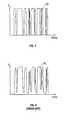
- FIG. 9is a receiver data eye diagram according to the prior art.
- FIG. 10is a waveform of a pre-compensated signal according to an embodiment of the invention.
- FIG. 11is a receiver eye diagram according to an embodiment of the invention.
- FIG. 12is a waveform illustrating a signal that is received from the serial bus of FIG. 1 according to an embodiment of the invention.
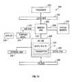
- FIG. 13is a schematic diagram of a computer system according to an embodiment of the invention.
- an embodiment 8 of a serial bus communication system in accordance with the inventionincludes a transmitter 10 that is constructed to pre-compensate digital signals before communicating the digital signals to conductive signal lines of a serial bus 16 .
- the serial bus 16distorts signals that propagate over the serial bus 16 .
- the transmitter 10includes a filter 12 for each conductive signal line of the serial bus 16 , and each filter 12 is designed to specifically pre-compensate for the distortion that is introduced by the associated signal line.
- each filter 12(a digital signal processing filter, for example) receives an indication of a particular digital signal from an interface 11 of the transmitter 10 .
- the filter 12introduces the appropriate distortion to the signal to pre-compensate the signal to cancel the distortion that is introduced by the associated signal line of the serial bus 16 . Due to this arrangement, a receiver 20 (of the system 8 ) may receive substantially undistorted signals from the serial bus 16 .
- each signal line (a copper line, for example) of the serial bus 16has electrical characteristics that may be modeled by the following partial differential equations:
- v[z,t]” and “i[z,t]”represent the voltage and current, respectively, at a particular position z along the signal line at time t;
- rrepresents a resistance of the line;
- grepresents the leakage conductance of the insulation that surrounds the line;
- lrepresents an inductance of the line; and
- crepresents a capacitance of the line.
- the “r,” “g,” “l,” and “c” valuesmay be expressed as a per unit quantity. For example, “r” may represent a resistance per inch.
- Equation 3may be used to derive a resistance plot 30 that is depicted in FIG. 2 . As shown, the resistance of the signal line increases with increasing frequency. A more accurate cable model may be determined by directly measuring the resistance (and incremental inductance) per unit length. However, for purposes of simplicity, the model derived from Equation 3 is described herein.
- a transfer function that characterizes the distortion that is introduced by the signal linemay be derived.
- a magnitude plot 40 of this transfer functionis depicted in FIG. 3, and as shown, the magnitude of the transfer function decreases with increasing frequency.
- the signal linealso introduces an “excess phase shift,” a term that may be defined as the phase shift of a sine wave propagating through the signal line that is over and beyond the simple phase shift coming from the propagation time of the line.
- a plot 50 of the excess phaseis depicted in FIG. 4 .
- the plots 40 and 50define the transfer function that characterizes a distortion that may be introduced by a signal line of the serial bus 16 .
- the transfer function of the filter 12may be designed.
- the filter 12is constructed to impart a transfer function that is the exact reciprocal of the transfer function of the line (depicted in FIGS. 3 and 4 ), neglecting the propagation phase shift. Because of its transfer function, the filter 12 substantially compensates for the distortion that is introduced by the signal line.
- a magnitude plot 120(see FIG. 5) of the transfer function of the filter 12 is mathematically the inverse of the magnitude plot 40 (see FIG. 3) of the conductive line, i.e., the combination of the two transfer functions produces a gain of unity.
- an excess phase plot 130(see FIG. 6) of the transfer function of the filter 12 is an inverse of the excess phase plot 50 of the signal line, i.e., the combination of the two transfer functions produces an excess phase shift of zero degrees.
- the use of the filter 12is to be contrasted to an arrangement that does not compensate for the distortion that is introduced by the signal line.
- a simulationwas performed in which a non-return-to-zero (NTZ) signal 80 (see FIG. 7) was communicated to a signal line at one end to form a corresponding signal 90 (see FIG. 8) at the other end of the signal line. Comparing the signals 80 and 90 , it is noted that the signal line both introduces a propagation delay and distorts any otherwise well-defined logic transitions in the signal 80 . Due to this distortion, the data eye at the receiver may be substantially minimized.
- NTZnon-return-to-zero
- FIG. 10depicts a signal 130 (at the output terminal of the transmitter 10 ) that is generated by passing the uncompensated signal 80 (see FIG. 7) through the filter 12 .
- the signal 130includes overshoots 132 and undershoots 133 on its rising and falling edges, respectively.
- the signal 130when routed through a signal line of the serial bus 16 , produces a signal 140 (see FIG. 12) near the receiver 20 .
- the signal 140is a near duplicate to the uncompensated signal 80 .
- the filter 12may be used to obtain a data eye diagram that is plotted in FIG. 11 .
- the data eye diagrammay be formed from complementary signals 144 and 146 and demonstrates the minimal dispersion that occurs with the use of the pre-compensation filter 12 .
- the transmitter 10may be part of a computer system 200 .
- the computer system 200may include a processor 202 (a microprocessor, for example) that is coupled to a local bus 204 .
- a north bridge, or memory hub 206that interfaces the local bus 204 to a memory bus 208 that is coupled to a system memory 210 .
- the memory hub 206also provides interfaces, for example, to an Accelerated Graphics Port (AGP) bus 212 and a hub link 218 .
- a graphics accelerator 214is coupled to the AGP bus 212 and may drive a display 216 .
- the AGPis described in detail in the Accelerated Graphics Port Interface Specification, Revision 1.0, published on Jul. 31, 1996, by Intel Corporation of Santa Clara, Calif.
- the hub link 218establishes communication between the memory hub 206 and an input/output (I/O) hub 220 that functions as a south bridge.
- I/Oinput/output
- the I/O hub 220may provide an interface to an I/O expansion bus 222 and a Peripheral Component Interconnect (PCI) bus 224 .
- PCIPeripheral Component Interconnect
- the PCI Specificationis available from The PCI Special Interest Group, Portland, Oreg. 97214.
Landscapes
- Engineering & Computer Science (AREA)
- Power Engineering (AREA)
- Computer Networks & Wireless Communication (AREA)
- Signal Processing (AREA)
- Dc Digital Transmission (AREA)
- Cable Transmission Systems, Equalization Of Radio And Reduction Of Echo (AREA)
Abstract
Description
The invention relates to a serial bus communication system.
A serial bus typically distorts signals that propagate across the bus. For example, the serial bus may include conductive signal lines (copper lines, for example) to communicate digital signals from a transmitter to a receiver. The signal lines typically introduce a dispersive transfer function to the fourier components of the digital signals. As a result of this dispersive transfer function, data communication may not exceed a maximum data communication rate (typically expressed in terms of Megabits/sec Kilometer). Otherwise, if communication of the data above the maximum data communication rate is attempted, the lines may attenuate the magnitudes of the digital signals and shift the phases of the digital signals to fully close the receiver's “eye opening,” an opening established by the time that is available at the receiver to re-clock the data and the voltage difference at the receiver between the logic one and the logic zero voltage levels.
Several techniques may be used to compensate for the distortion that is introduced by the serial bus. For example, a technique called adaptive equalization may be used. With adaptive equalization, the distorted digital signals are received from the lines of the serial bus and are routed through analog filters that are coupled between the lines of the serial bus and the receiver. These analog filters apply gain/loss factors and phase shifts to the distorted digital signals for purposes of removing the distortion. However, a potential problem with this approach is the cost and complexity that are associated with analog filtering.
Another technique to compensate for the distortion that is introduced by the serial bus is pre-compensation, a technique in which a distortion function is applied to each digital signal before the digital signal is communicated to the signal line of the serial bus. Due to this compensation, the digital signals should appear relatively undistorted near the receiver. However, in the past, an estimation of the distortion that is introduced by a particular line of the serial bus was used to develop pre-compensation filters to reduce the distortion. Unfortunately, this estimation may be imprecise, and to the extent that the estimation is incorrect, the digital signal may appear substantially distorted at the receiver.
Thus, there is a continuing need for an arrangement to more precisely compensate for distortion that is introduced by a serial bus.
FIG. 1 is a schematic diagram of a serial bus communication system according to an embodiment of the invention.
FIG. 2 is a resistance versus frequency plot for a conductive signal line of the serial bus of FIG.1.
FIG. 3 is a magnitude plot of a distortion introduced by the serial bus of FIG.1.
FIG. 4 is a phase plot of the distortion introduced by the serial bus of FIG.1.
FIG. 5 is a magnitude plot of the frequency response of a pre-compensation filter of FIG.1.
FIG. 6 is a phase plot of the frequency response of the pre-compensation filter of FIG.1.
FIG. 7 is a waveform illustrating a signal that is furnished to the serial bus.
FIG. 8 is a waveform illustrating a signal that is received from the serial bus according to the prior art.
FIG. 9 is a receiver data eye diagram according to the prior art.
FIG. 10 is a waveform of a pre-compensated signal according to an embodiment of the invention.
FIG. 11 is a receiver eye diagram according to an embodiment of the invention.
FIG. 12 is a waveform illustrating a signal that is received from the serial bus of FIG. 1 according to an embodiment of the invention.
FIG. 13 is a schematic diagram of a computer system according to an embodiment of the invention.
Referring to FIG. 1, anembodiment 8 of a serial bus communication system in accordance with the invention includes atransmitter 10 that is constructed to pre-compensate digital signals before communicating the digital signals to conductive signal lines of aserial bus 16. In this manner, theserial bus 16 distorts signals that propagate over theserial bus 16. However, as described below, thetransmitter 10 includes afilter 12 for each conductive signal line of theserial bus 16, and eachfilter 12 is designed to specifically pre-compensate for the distortion that is introduced by the associated signal line. In this manner, in some embodiments, each filter12 (a digital signal processing filter, for example) receives an indication of a particular digital signal from aninterface 11 of thetransmitter 10. Thefilter 12 introduces the appropriate distortion to the signal to pre-compensate the signal to cancel the distortion that is introduced by the associated signal line of theserial bus 16. Due to this arrangement, a receiver20 (of the system8) may receive substantially undistorted signals from theserial bus 16.
More particularly, in some embodiments, each signal line (a copper line, for example) of theserial bus 16 has electrical characteristics that may be modeled by the following partial differential equations:
where “v[z,t]” and “i[z,t]” represent the voltage and current, respectively, at a particular position z along the signal line at time t; “r” represents a resistance of the line; “g” represents the leakage conductance of the insulation that surrounds the line; “l” represents an inductance of the line; and “c” represents a capacitance of the line. The “r,” “g,” “l,” and “c” values may be expressed as a per unit quantity. For example, “r” may represent a resistance per inch.
The resistance of the signal line varies with frequency due to the skin depth effect. Taking this variation into account, a simple electrical model of the signal line may be a model in which the insulation that surrounds the signal line has no leakage (g=0), and the signal line has a resistance that changes with frequency (due to the skin depth effect), as described by the following equations:

where “rdc” is the DC resistance of the signal line, and “f0” is a frequency near 1 Megahertz (MHz). The skin depth effect increases the resistance per unit length of the signal line and also adds an incremental inductive reactance. Equation 3 may be used to derive aresistance plot 30 that is depicted in FIG.2. As shown, the resistance of the signal line increases with increasing frequency. A more accurate cable model may be determined by directly measuring the resistance (and incremental inductance) per unit length. However, for purposes of simplicity, the model derived from Equation 3 is described herein.
Thus, using this model, a transfer function that characterizes the distortion that is introduced by the signal line may be derived. In this manner, amagnitude plot 40 of this transfer function is depicted in FIG. 3, and as shown, the magnitude of the transfer function decreases with increasing frequency. Besides changing the magnitude of the signal, the signal line also introduces an “excess phase shift,” a term that may be defined as the phase shift of a sine wave propagating through the signal line that is over and beyond the simple phase shift coming from the propagation time of the line. Aplot 50 of the excess phase is depicted in FIG.4. Thus, theplots serial bus 16.
Due to the above-described mathematical modeling of the signal line, the transfer function of the filter12 (see FIG. 1) may be designed. In this manner, in some embodiments, thefilter 12 is constructed to impart a transfer function that is the exact reciprocal of the transfer function of the line (depicted in FIGS.3 and4), neglecting the propagation phase shift. Because of its transfer function, thefilter 12 substantially compensates for the distortion that is introduced by the signal line. Thus, a magnitude plot120 (see FIG. 5) of the transfer function of thefilter 12 is mathematically the inverse of the magnitude plot40 (see FIG. 3) of the conductive line, i.e., the combination of the two transfer functions produces a gain of unity. Similarly, an excess phase plot130 (see FIG. 6) of the transfer function of thefilter 12 is an inverse of theexcess phase plot 50 of the signal line, i.e., the combination of the two transfer functions produces an excess phase shift of zero degrees.
The use of thefilter 12 is to be contrasted to an arrangement that does not compensate for the distortion that is introduced by the signal line. To illustrate this point, a simulation was performed in which a non-return-to-zero (NTZ) signal80 (see FIG. 7) was communicated to a signal line at one end to form a corresponding signal90 (see FIG. 8) at the other end of the signal line. Comparing thesignals signal 80. Due to this distortion, the data eye at the receiver may be substantially minimized.
To demonstrate this point, the following simulation was conducted to produce adata eye 103 that is depicted in FIG.9. In this simulation, uncompensated signals that have a logic one to logic zero transition at ideally time T1were communicated across the signal line to producesignals 100. Similarly, uncompensated signals that have a logic zero to logic one transition at ideally time T1were communicated across the conductive line to producesignals 101 that are also plotted in FIG.9. To complete the plot of thedata eye 103, uncompensated signals that have a logic one to logic zero transition at ideally time T0were communicated across the conductive line to producesignals 99 that appear in FIG. 9; and uncompensated signals that have a logic zero to logic one transition at ideally time T0were communicated across the conductive line to producesignals 98 that are also plotted in FIG.9. Thus, as shown, without compensation of the distortion that is introduced by the serial bus, the logic transitions have large rise and fall times that decrease the size of thedata eye 103 and degrade the quality of data communication across theserial bus 16.
The above-described results are to be compared to the simulated signals that occur with the use of thefilter 12. In this manner, FIG. 10 depicts a signal130 (at the output terminal of the transmitter10) that is generated by passing the uncompensated signal80 (see FIG. 7) through thefilter 12. As shown, thesignal 130 includes overshoots132 and undershoots133 on its rising and falling edges, respectively. However, thesignal 130, when routed through a signal line of theserial bus 16, produces a signal140 (see FIG. 12) near thereceiver 20. Thesignal 140 is a near duplicate to theuncompensated signal 80.
Thus, by using thefilter 12, a data eye diagram that is plotted in FIG. 11 may be obtained. The data eye diagram may be formed fromcomplementary signals pre-compensation filter 12.
Referring to FIG. 13, in some embodiments, thetransmitter 10 may be part of acomputer system 200. In this manner, thecomputer system 200 may include a processor202 (a microprocessor, for example) that is coupled to alocal bus 204. Also coupled to thelocal bus 204 is a north bridge, ormemory hub 206, that interfaces thelocal bus 204 to amemory bus 208 that is coupled to asystem memory 210. Thememory hub 206 also provides interfaces, for example, to an Accelerated Graphics Port (AGP)bus 212 and ahub link 218. Agraphics accelerator 214 is coupled to theAGP bus 212 and may drive adisplay 216. The AGP is described in detail in the Accelerated Graphics Port Interface Specification, Revision 1.0, published on Jul. 31, 1996, by Intel Corporation of Santa Clara, Calif.
Thehub link 218 establishes communication between thememory hub 206 and an input/output (I/O)hub 220 that functions as a south bridge. In this manner, the I/O hub 220 may provide an interface to an I/O expansion bus 222 and a Peripheral Component Interconnect (PCI)bus 224. The PCI Specification is available from The PCI Special Interest Group, Portland, Oreg. 97214.
While the invention has been disclosed with respect to a limited number of embodiments, those skilled in the art, having the benefit of this disclosure, will appreciate numerous modifications and variations therefrom. It is intended that the appended claims cover all such modifications and variations as fall within the true spirit and scope of the invention.
Claims (15)
1. A system comprising:
a serial bus to propagate an unmodulated digital signal, the serial bus capable of introducing a distortion characterized by a first frequency response;
a receiver coupled to the serial bus to receive the unmodulated digital signal; and
a transmitter coupled to the serial bus to transmit the unmodulated digital signal, the transmitter including a filter having a second frequency response to substantially cancel the distortion introduced by the serial bus.
2. The system ofclaim 1 , wherein the first frequency response is substantially an inverse of the second frequency response.
3. The system ofclaim 1 , wherein the distortion is caused at least in part by a skin depth effect of a conductive line of the serial bus.
4. The system ofclaim 1 , wherein the first frequency response has a first magnitude that is substantially an inverse of a second magnitude of the second frequency response.
5. The system ofclaim 1 , wherein the first frequency response has a first phase that is substantially an inverse of a second phase of the second frequency response.
6. A method comprising:
determining a first frequency response that characterizes a distortion introduced by a serial bus to an unmodulated digital signal that propagates along the serial bus;
designing a filter to have a second frequency response to substantially cancel the distortion; and
transmitting a signal to the serial bus through the filter.
7. The method ofclaim 6 , wherein the first frequency response is an inverse of the second frequency response.
8. The method ofclaim 6 , wherein the distortion is caused at least in part by a skin depth effect of a conductive line of the cable.
9. The method ofclaim 6 , wherein the first frequency response has a first magnitude that is substantially an inverse of a second magnitude of the second frequency response.
10. The method ofclaim 6 , wherein the first frequency response has a first phase that is substantially an inverse of a second phase of the second frequency response.
11. A serial bus transmitter comprising:
a driver to communicate a first unmodulated digital signal to a serial bus, the serial bus having a distortion characterized by a first frequency response;
a filter coupled to the driver, the filter having a second frequency response to substantially cancel out the distortion.
12. The transmitter ofclaim 11 , wherein the first frequency response is an inverse of the second frequency response.
13. The transmitter ofclaim 11 , wherein the first frequency response has a first magnitude that is substantially an inverse of a second magnitude of the second frequency response.
14. The transmitter ofclaim 11 , wherein the first frequency response has a first phase that is substantially an inverse of a second phase of the second frequency response.
15. The transmitter ofclaim 11 , wherein the distortion is caused at least in part by a skin depth effect of a conductive line of the cable.
Priority Applications (1)
| Application Number | Priority Date | Filing Date | Title |
|---|---|---|---|
| US09/495,264US6823023B1 (en) | 2000-01-31 | 2000-01-31 | Serial bus communication system |
Applications Claiming Priority (1)
| Application Number | Priority Date | Filing Date | Title |
|---|---|---|---|
| US09/495,264US6823023B1 (en) | 2000-01-31 | 2000-01-31 | Serial bus communication system |
Publications (1)
| Publication Number | Publication Date |
|---|---|
| US6823023B1true US6823023B1 (en) | 2004-11-23 |
Family
ID=33435288
Family Applications (1)
| Application Number | Title | Priority Date | Filing Date |
|---|---|---|---|
| US09/495,264Expired - LifetimeUS6823023B1 (en) | 2000-01-31 | 2000-01-31 | Serial bus communication system |
Country Status (1)
| Country | Link |
|---|---|
| US (1) | US6823023B1 (en) |
Cited By (42)
| Publication number | Priority date | Publication date | Assignee | Title |
|---|---|---|---|---|
| US20050146943A1 (en)* | 2003-08-28 | 2005-07-07 | Jeddeloh Joseph M. | Memory module and method having on-board data search capabilities and processor-based system using such memory modules |
| US6980042B2 (en) | 2004-04-05 | 2005-12-27 | Micron Technology, Inc. | Delay line synchronizer apparatus and method |
| US20060067387A1 (en)* | 2004-09-30 | 2006-03-30 | Ahmed Ali U | Transmit adaptive equalization using ordered sets |
| US7047351B2 (en) | 2002-08-16 | 2006-05-16 | Micron Technology, Inc. | Memory hub bypass circuit and method |
| US7106611B2 (en) | 2002-09-09 | 2006-09-12 | Micron Technology, Inc. | Wavelength division multiplexed memory module, memory system and method |
| US7107415B2 (en) | 2003-06-20 | 2006-09-12 | Micron Technology, Inc. | Posted write buffers and methods of posting write requests in memory modules |
| US7117316B2 (en) | 2002-08-05 | 2006-10-03 | Micron Technology, Inc. | Memory hub and access method having internal row caching |
| US7120743B2 (en) | 2003-10-20 | 2006-10-10 | Micron Technology, Inc. | Arbitration system and method for memory responses in a hub-based memory system |
| US7120723B2 (en) | 2004-03-25 | 2006-10-10 | Micron Technology, Inc. | System and method for memory hub-based expansion bus |
| US7120727B2 (en) | 2003-06-19 | 2006-10-10 | Micron Technology, Inc. | Reconfigurable memory module and method |
| US7133972B2 (en) | 2002-06-07 | 2006-11-07 | Micron Technology, Inc. | Memory hub with internal cache and/or memory access prediction |
| US7133991B2 (en) | 2003-08-20 | 2006-11-07 | Micron Technology, Inc. | Method and system for capturing and bypassing memory transactions in a hub-based memory system |
| US7136958B2 (en) | 2003-08-28 | 2006-11-14 | Micron Technology, Inc. | Multiple processor system and method including multiple memory hub modules |
| US7162567B2 (en) | 2004-05-14 | 2007-01-09 | Micron Technology, Inc. | Memory hub and method for memory sequencing |
| US7181584B2 (en) | 2004-02-05 | 2007-02-20 | Micron Technology, Inc. | Dynamic command and/or address mirroring system and method for memory modules |
| US7180522B2 (en) | 2000-06-23 | 2007-02-20 | Micron Technology, Inc. | Apparatus and method for distributed memory control in a graphics processing system |
| US7188219B2 (en) | 2004-01-30 | 2007-03-06 | Micron Technology, Inc. | Buffer control system and method for a memory system having outstanding read and write request buffers |
| US7194593B2 (en) | 2003-09-18 | 2007-03-20 | Micron Technology, Inc. | Memory hub with integrated non-volatile memory |
| US7200024B2 (en) | 2002-08-02 | 2007-04-03 | Micron Technology, Inc. | System and method for optically interconnecting memory devices |
| US7210059B2 (en) | 2003-08-19 | 2007-04-24 | Micron Technology, Inc. | System and method for on-board diagnostics of memory modules |
| US7213082B2 (en) | 2004-03-29 | 2007-05-01 | Micron Technology, Inc. | Memory hub and method for providing memory sequencing hints |
| US7222197B2 (en) | 2003-07-22 | 2007-05-22 | Micron Technology, Inc. | Apparatus and method for direct memory access in a hub-based memory system |
| US7222213B2 (en) | 2004-05-17 | 2007-05-22 | Micron Technology, Inc. | System and method for communicating the synchronization status of memory modules during initialization of the memory modules |
| US7234070B2 (en) | 2003-10-27 | 2007-06-19 | Micron Technology, Inc. | System and method for using a learning sequence to establish communications on a high-speed nonsynchronous interface in the absence of clock forwarding |
| US7242213B2 (en) | 2003-06-11 | 2007-07-10 | Micron Technology, Inc. | Memory module and method having improved signal routing topology |
| US7249236B2 (en) | 2002-08-29 | 2007-07-24 | Micron Technology, Inc. | Method and system for controlling memory accesses to memory modules having a memory hub architecture |
| US7254331B2 (en) | 2002-08-09 | 2007-08-07 | Micron Technology, Inc. | System and method for multiple bit optical data transmission in memory systems |
| US7257683B2 (en) | 2004-03-24 | 2007-08-14 | Micron Technology, Inc. | Memory arbitration system and method having an arbitration packet protocol |
| US7260685B2 (en) | 2003-06-20 | 2007-08-21 | Micron Technology, Inc. | Memory hub and access method having internal prefetch buffers |
| US7310748B2 (en) | 2004-06-04 | 2007-12-18 | Micron Technology, Inc. | Memory hub tester interface and method for use thereof |
| US7310752B2 (en) | 2003-09-12 | 2007-12-18 | Micron Technology, Inc. | System and method for on-board timing margin testing of memory modules |
| US7363419B2 (en) | 2004-05-28 | 2008-04-22 | Micron Technology, Inc. | Method and system for terminating write commands in a hub-based memory system |
| US7392331B2 (en) | 2004-08-31 | 2008-06-24 | Micron Technology, Inc. | System and method for transmitting data packets in a computer system having a memory hub architecture |
| US7412574B2 (en) | 2004-02-05 | 2008-08-12 | Micron Technology, Inc. | System and method for arbitration of memory responses in a hub-based memory system |
| US7428644B2 (en) | 2003-06-20 | 2008-09-23 | Micron Technology, Inc. | System and method for selective memory module power management |
| US7447240B2 (en) | 2004-03-29 | 2008-11-04 | Micron Technology, Inc. | Method and system for synchronizing communications links in a hub-based memory system |
| US7519788B2 (en) | 2004-06-04 | 2009-04-14 | Micron Technology, Inc. | System and method for an asynchronous data buffer having buffer write and read pointers |
| US7590797B2 (en) | 2004-04-08 | 2009-09-15 | Micron Technology, Inc. | System and method for optimizing interconnections of components in a multichip memory module |
| US7788451B2 (en) | 2004-02-05 | 2010-08-31 | Micron Technology, Inc. | Apparatus and method for data bypass for a bi-directional data bus in a hub-based memory sub-system |
| US7805586B2 (en) | 2002-08-29 | 2010-09-28 | Micron Technology, Inc. | System and method for optimizing interconnections of memory devices in a multichip module |
| US8775764B2 (en) | 2004-03-08 | 2014-07-08 | Micron Technology, Inc. | Memory hub architecture having programmable lane widths |
| US8880833B2 (en) | 2003-12-29 | 2014-11-04 | Micron Technology, Inc. | System and method for read synchronization of memory modules |
Citations (5)
| Publication number | Priority date | Publication date | Assignee | Title |
|---|---|---|---|---|
| US6140822A (en)* | 1997-05-29 | 2000-10-31 | Williams; Thomas H. | System for signal path characterization with a reference signal using stepped-frequency increments |
| US6194942B1 (en)* | 2000-01-19 | 2001-02-27 | Cable Vision Electronics Co., Ltd. | Predistortion circuit for linearization of signals |
| US6285859B1 (en)* | 1998-02-16 | 2001-09-04 | Alcatel | Method for predistortion of a signal transmitted between two units of a telecommunications network and a unit for carrying out the method |
| US6373902B1 (en)* | 1997-06-19 | 2002-04-16 | Samsung Electronics Co., Ltd | Device and method for linearizing transmitter in digital communication system |
| US6516025B1 (en)* | 1999-04-29 | 2003-02-04 | Texas Instruments Incorporated | High-speed upstream modem communication |
- 2000
- 2000-01-31USUS09/495,264patent/US6823023B1/ennot_activeExpired - Lifetime
Patent Citations (5)
| Publication number | Priority date | Publication date | Assignee | Title |
|---|---|---|---|---|
| US6140822A (en)* | 1997-05-29 | 2000-10-31 | Williams; Thomas H. | System for signal path characterization with a reference signal using stepped-frequency increments |
| US6373902B1 (en)* | 1997-06-19 | 2002-04-16 | Samsung Electronics Co., Ltd | Device and method for linearizing transmitter in digital communication system |
| US6285859B1 (en)* | 1998-02-16 | 2001-09-04 | Alcatel | Method for predistortion of a signal transmitted between two units of a telecommunications network and a unit for carrying out the method |
| US6516025B1 (en)* | 1999-04-29 | 2003-02-04 | Texas Instruments Incorporated | High-speed upstream modem communication |
| US6194942B1 (en)* | 2000-01-19 | 2001-02-27 | Cable Vision Electronics Co., Ltd. | Predistortion circuit for linearization of signals |
Cited By (124)
| Publication number | Priority date | Publication date | Assignee | Title |
|---|---|---|---|---|
| US7180522B2 (en) | 2000-06-23 | 2007-02-20 | Micron Technology, Inc. | Apparatus and method for distributed memory control in a graphics processing system |
| US8499127B2 (en) | 2002-06-07 | 2013-07-30 | Round Rock Research, Llc | Memory hub with internal cache and/or memory access prediction |
| US7945737B2 (en) | 2002-06-07 | 2011-05-17 | Round Rock Research, Llc | Memory hub with internal cache and/or memory access prediction |
| US8195918B2 (en) | 2002-06-07 | 2012-06-05 | Round Rock Research, Llc | Memory hub with internal cache and/or memory access prediction |
| US7644253B2 (en) | 2002-06-07 | 2010-01-05 | Micron Technology, Inc. | Memory hub with internal cache and/or memory access prediction |
| US7133972B2 (en) | 2002-06-07 | 2006-11-07 | Micron Technology, Inc. | Memory hub with internal cache and/or memory access prediction |
| US7200024B2 (en) | 2002-08-02 | 2007-04-03 | Micron Technology, Inc. | System and method for optically interconnecting memory devices |
| US7382639B2 (en) | 2002-08-02 | 2008-06-03 | Micron Technology, Inc. | System and method for optically interconnecting memory devices |
| US7289347B2 (en) | 2002-08-02 | 2007-10-30 | Micron Technology, Inc. | System and method for optically interconnecting memory devices |
| US7411807B2 (en) | 2002-08-02 | 2008-08-12 | Micron Technology, Inc. | System and method for optically interconnecting memory devices |
| US7117316B2 (en) | 2002-08-05 | 2006-10-03 | Micron Technology, Inc. | Memory hub and access method having internal row caching |
| US8954687B2 (en) | 2002-08-05 | 2015-02-10 | Micron Technology, Inc. | Memory hub and access method having a sequencer and internal row caching |
| US7489875B2 (en) | 2002-08-09 | 2009-02-10 | Micron Technology, Inc. | System and method for multiple bit optical data transmission in memory systems |
| US7254331B2 (en) | 2002-08-09 | 2007-08-07 | Micron Technology, Inc. | System and method for multiple bit optical data transmission in memory systems |
| US7047351B2 (en) | 2002-08-16 | 2006-05-16 | Micron Technology, Inc. | Memory hub bypass circuit and method |
| US7149874B2 (en) | 2002-08-16 | 2006-12-12 | Micron Technology, Inc. | Memory hub bypass circuit and method |
| US7415567B2 (en) | 2002-08-16 | 2008-08-19 | Micron Technology, Inc. | Memory hub bypass circuit and method |
| US7805586B2 (en) | 2002-08-29 | 2010-09-28 | Micron Technology, Inc. | System and method for optimizing interconnections of memory devices in a multichip module |
| US7249236B2 (en) | 2002-08-29 | 2007-07-24 | Micron Technology, Inc. | Method and system for controlling memory accesses to memory modules having a memory hub architecture |
| US7836252B2 (en) | 2002-08-29 | 2010-11-16 | Micron Technology, Inc. | System and method for optimizing interconnections of memory devices in a multichip module |
| US7908452B2 (en) | 2002-08-29 | 2011-03-15 | Round Rock Research, Llc | Method and system for controlling memory accesses to memory modules having a memory hub architecture |
| US8190819B2 (en) | 2002-08-29 | 2012-05-29 | Micron Technology, Inc. | System and method for optimizing interconnections of memory devices in a multichip module |
| US7716444B2 (en) | 2002-08-29 | 2010-05-11 | Round Rock Research, Llc | Method and system for controlling memory accesses to memory modules having a memory hub architecture |
| US8234479B2 (en) | 2002-08-29 | 2012-07-31 | Round Rock Research, Llc | System for controlling memory accesses to memory modules having a memory hub architecture |
| US8086815B2 (en) | 2002-08-29 | 2011-12-27 | Round Rock Research, Llc | System for controlling memory accesses to memory modules having a memory hub architecture |
| US7106611B2 (en) | 2002-09-09 | 2006-09-12 | Micron Technology, Inc. | Wavelength division multiplexed memory module, memory system and method |
| US7282947B2 (en) | 2003-06-11 | 2007-10-16 | Micron Technology, Inc. | Memory module and method having improved signal routing topology |
| US7746095B2 (en) | 2003-06-11 | 2010-06-29 | Round Rock Research, Llc | Memory module and method having improved signal routing topology |
| US7242213B2 (en) | 2003-06-11 | 2007-07-10 | Micron Technology, Inc. | Memory module and method having improved signal routing topology |
| US7245145B2 (en) | 2003-06-11 | 2007-07-17 | Micron Technology, Inc. | Memory module and method having improved signal routing topology |
| US7557601B2 (en) | 2003-06-11 | 2009-07-07 | Micron Technology, Inc. | Memory module and method having improved signal routing topology |
| US7818712B2 (en) | 2003-06-19 | 2010-10-19 | Round Rock Research, Llc | Reconfigurable memory module and method |
| US7966444B2 (en) | 2003-06-19 | 2011-06-21 | Round Rock Research, Llc | Reconfigurable memory module and method |
| US8732383B2 (en) | 2003-06-19 | 2014-05-20 | Round Rock Research, Llc | Reconfigurable memory module and method |
| US8200884B2 (en) | 2003-06-19 | 2012-06-12 | Round Rock Research, Llc | Reconfigurable memory module and method |
| US7120727B2 (en) | 2003-06-19 | 2006-10-10 | Micron Technology, Inc. | Reconfigurable memory module and method |
| US7437579B2 (en) | 2003-06-20 | 2008-10-14 | Micron Technology, Inc. | System and method for selective memory module power management |
| US7428644B2 (en) | 2003-06-20 | 2008-09-23 | Micron Technology, Inc. | System and method for selective memory module power management |
| US7260685B2 (en) | 2003-06-20 | 2007-08-21 | Micron Technology, Inc. | Memory hub and access method having internal prefetch buffers |
| US7412566B2 (en) | 2003-06-20 | 2008-08-12 | Micron Technology, Inc. | Memory hub and access method having internal prefetch buffers |
| US8127081B2 (en) | 2003-06-20 | 2012-02-28 | Round Rock Research, Llc | Memory hub and access method having internal prefetch buffers |
| US7107415B2 (en) | 2003-06-20 | 2006-09-12 | Micron Technology, Inc. | Posted write buffers and methods of posting write requests in memory modules |
| US8209445B2 (en) | 2003-07-22 | 2012-06-26 | Round Rock Research, Llc | Apparatus and method for direct memory access in a hub-based memory system |
| US7222197B2 (en) | 2003-07-22 | 2007-05-22 | Micron Technology, Inc. | Apparatus and method for direct memory access in a hub-based memory system |
| US7389364B2 (en) | 2003-07-22 | 2008-06-17 | Micron Technology, Inc. | Apparatus and method for direct memory access in a hub-based memory system |
| US7966430B2 (en) | 2003-07-22 | 2011-06-21 | Round Rock Research, Llc | Apparatus and method for direct memory access in a hub-based memory system |
| US7913122B2 (en) | 2003-08-19 | 2011-03-22 | Round Rock Research, Llc | System and method for on-board diagnostics of memory modules |
| US7516363B2 (en) | 2003-08-19 | 2009-04-07 | Micron Technology, Inc. | System and method for on-board diagnostics of memory modules |
| US7278060B2 (en) | 2003-08-19 | 2007-10-02 | Micron Technology, Inc. | System and method for on-board diagnostics of memory modules |
| US7210059B2 (en) | 2003-08-19 | 2007-04-24 | Micron Technology, Inc. | System and method for on-board diagnostics of memory modules |
| US7133991B2 (en) | 2003-08-20 | 2006-11-07 | Micron Technology, Inc. | Method and system for capturing and bypassing memory transactions in a hub-based memory system |
| US7251714B2 (en) | 2003-08-20 | 2007-07-31 | Micron Technology, Inc. | Method and system for capturing and bypassing memory transactions in a hub-based memory system |
| US8244952B2 (en) | 2003-08-28 | 2012-08-14 | Round Rock Research, Llc | Multiple processor system and method including multiple memory hub modules |
| US20050146943A1 (en)* | 2003-08-28 | 2005-07-07 | Jeddeloh Joseph M. | Memory module and method having on-board data search capabilities and processor-based system using such memory modules |
| US7873775B2 (en) | 2003-08-28 | 2011-01-18 | Round Rock Research, Llc | Multiple processor system and method including multiple memory hub modules |
| US7136958B2 (en) | 2003-08-28 | 2006-11-14 | Micron Technology, Inc. | Multiple processor system and method including multiple memory hub modules |
| US9082461B2 (en) | 2003-08-28 | 2015-07-14 | Round Rock Research, Llc | Multiple processor system and method including multiple memory hub modules |
| US7386649B2 (en) | 2003-08-28 | 2008-06-10 | Micron Technology, Inc. | Multiple processor system and method including multiple memory hub modules |
| US7581055B2 (en) | 2003-08-28 | 2009-08-25 | Micron Technology, Inc. | Multiple processor system and method including multiple memory hub modules |
| US7958412B2 (en) | 2003-09-12 | 2011-06-07 | Round Rock Research, Llc | System and method for on-board timing margin testing of memory modules |
| US7689879B2 (en) | 2003-09-12 | 2010-03-30 | Micron Technology, Inc. | System and method for on-board timing margin testing of memory modules |
| US7310752B2 (en) | 2003-09-12 | 2007-12-18 | Micron Technology, Inc. | System and method for on-board timing margin testing of memory modules |
| US7975122B2 (en) | 2003-09-18 | 2011-07-05 | Round Rock Research, Llc | Memory hub with integrated non-volatile memory |
| US7490211B2 (en) | 2003-09-18 | 2009-02-10 | Micron Technology, Inc. | Memory hub with integrated non-volatile memory |
| US7194593B2 (en) | 2003-09-18 | 2007-03-20 | Micron Technology, Inc. | Memory hub with integrated non-volatile memory |
| US8832404B2 (en) | 2003-09-18 | 2014-09-09 | Round Rock Research, Llc | Memory hub with integrated non-volatile memory |
| US7120743B2 (en) | 2003-10-20 | 2006-10-10 | Micron Technology, Inc. | Arbitration system and method for memory responses in a hub-based memory system |
| US8589643B2 (en) | 2003-10-20 | 2013-11-19 | Round Rock Research, Llc | Arbitration system and method for memory responses in a hub-based memory system |
| US7461286B2 (en) | 2003-10-27 | 2008-12-02 | Micron Technology, Inc. | System and method for using a learning sequence to establish communications on a high-speed nonsynchronous interface in the absence of clock forwarding |
| US7234070B2 (en) | 2003-10-27 | 2007-06-19 | Micron Technology, Inc. | System and method for using a learning sequence to establish communications on a high-speed nonsynchronous interface in the absence of clock forwarding |
| US8880833B2 (en) | 2003-12-29 | 2014-11-04 | Micron Technology, Inc. | System and method for read synchronization of memory modules |
| US7188219B2 (en) | 2004-01-30 | 2007-03-06 | Micron Technology, Inc. | Buffer control system and method for a memory system having outstanding read and write request buffers |
| US8788765B2 (en) | 2004-01-30 | 2014-07-22 | Micron Technology, Inc. | Buffer control system and method for a memory system having outstanding read and write request buffers |
| US8504782B2 (en) | 2004-01-30 | 2013-08-06 | Micron Technology, Inc. | Buffer control system and method for a memory system having outstanding read and write request buffers |
| US7788451B2 (en) | 2004-02-05 | 2010-08-31 | Micron Technology, Inc. | Apparatus and method for data bypass for a bi-directional data bus in a hub-based memory sub-system |
| US8694735B2 (en) | 2004-02-05 | 2014-04-08 | Micron Technology, Inc. | Apparatus and method for data bypass for a bi-directional data bus in a hub-based memory sub-system |
| US8291173B2 (en) | 2004-02-05 | 2012-10-16 | Micron Technology, Inc. | Apparatus and method for data bypass for a bi-directional data bus in a hub-based memory sub-system |
| US9164937B2 (en) | 2004-02-05 | 2015-10-20 | Micron Technology, Inc. | Apparatus and method for data bypass for a bi-directional data bus in a hub-based memory sub-system |
| US7181584B2 (en) | 2004-02-05 | 2007-02-20 | Micron Technology, Inc. | Dynamic command and/or address mirroring system and method for memory modules |
| US7412574B2 (en) | 2004-02-05 | 2008-08-12 | Micron Technology, Inc. | System and method for arbitration of memory responses in a hub-based memory system |
| US7546435B2 (en) | 2004-02-05 | 2009-06-09 | Micron Technology. Inc. | Dynamic command and/or address mirroring system and method for memory modules |
| US8775764B2 (en) | 2004-03-08 | 2014-07-08 | Micron Technology, Inc. | Memory hub architecture having programmable lane widths |
| US9274991B2 (en) | 2004-03-08 | 2016-03-01 | Micron Technology, Inc. | Memory hub architecture having programmable lane widths |
| US8082404B2 (en) | 2004-03-24 | 2011-12-20 | Micron Technology, Inc. | Memory arbitration system and method having an arbitration packet protocol |
| US8555006B2 (en) | 2004-03-24 | 2013-10-08 | Micron Technology, Inc. | Memory arbitration system and method having an arbitration packet protocol |
| US7412571B2 (en) | 2004-03-24 | 2008-08-12 | Micron Technology, Inc. | Memory arbitration system and method having an arbitration packet protocol |
| US9032166B2 (en) | 2004-03-24 | 2015-05-12 | Micron Technology, Inc. | Memory arbitration system and method having an arbitration packet protocol |
| US7257683B2 (en) | 2004-03-24 | 2007-08-14 | Micron Technology, Inc. | Memory arbitration system and method having an arbitration packet protocol |
| US8117371B2 (en) | 2004-03-25 | 2012-02-14 | Round Rock Research, Llc | System and method for memory hub-based expansion bus |
| US7610430B2 (en) | 2004-03-25 | 2009-10-27 | Micron Technology, Inc. | System and method for memory hub-based expansion bus |
| US7370134B2 (en) | 2004-03-25 | 2008-05-06 | Micron Technology, Inc. | System and method for memory hub-based expansion bus |
| US7120723B2 (en) | 2004-03-25 | 2006-10-10 | Micron Technology, Inc. | System and method for memory hub-based expansion bus |
| US7222210B2 (en) | 2004-03-25 | 2007-05-22 | Micron Technology, Inc. | System and method for memory hub-based expansion bus |
| US7899969B2 (en) | 2004-03-25 | 2011-03-01 | Round Rock Research, Llc | System and method for memory hub-based expansion bus |
| US7174409B2 (en) | 2004-03-25 | 2007-02-06 | Micron Technology, Inc. | System and method for memory hub-based expansion bus |
| US7206887B2 (en) | 2004-03-25 | 2007-04-17 | Micron Technology, Inc. | System and method for memory hub-based expansion bus |
| US7447240B2 (en) | 2004-03-29 | 2008-11-04 | Micron Technology, Inc. | Method and system for synchronizing communications links in a hub-based memory system |
| US7418526B2 (en) | 2004-03-29 | 2008-08-26 | Micron Technology, Inc. | Memory hub and method for providing memory sequencing hints |
| US7529273B2 (en) | 2004-03-29 | 2009-05-05 | Micron Technology, Inc. | Method and system for synchronizing communications links in a hub-based memory system |
| US7213082B2 (en) | 2004-03-29 | 2007-05-01 | Micron Technology, Inc. | Memory hub and method for providing memory sequencing hints |
| US7605631B2 (en) | 2004-04-05 | 2009-10-20 | Micron Technology, Inc. | Delay line synchronizer apparatus and method |
| US8164375B2 (en) | 2004-04-05 | 2012-04-24 | Round Rock Research, Llc | Delay line synchronizer apparatus and method |
| US6980042B2 (en) | 2004-04-05 | 2005-12-27 | Micron Technology, Inc. | Delay line synchronizer apparatus and method |
| US7590797B2 (en) | 2004-04-08 | 2009-09-15 | Micron Technology, Inc. | System and method for optimizing interconnections of components in a multichip memory module |
| US8438329B2 (en) | 2004-04-08 | 2013-05-07 | Micron Technology, Inc. | System and method for optimizing interconnections of components in a multichip memory module |
| US7870329B2 (en) | 2004-04-08 | 2011-01-11 | Micron Technology, Inc. | System and method for optimizing interconnections of components in a multichip memory module |
| US7562178B2 (en) | 2004-05-14 | 2009-07-14 | Micron Technology, Inc. | Memory hub and method for memory sequencing |
| US7162567B2 (en) | 2004-05-14 | 2007-01-09 | Micron Technology, Inc. | Memory hub and method for memory sequencing |
| US7353320B2 (en) | 2004-05-14 | 2008-04-01 | Micron Technology, Inc. | Memory hub and method for memory sequencing |
| US7266633B2 (en) | 2004-05-17 | 2007-09-04 | Micron Technology, Inc. | System and method for communicating the synchronization status of memory modules during initialization of the memory modules |
| US7222213B2 (en) | 2004-05-17 | 2007-05-22 | Micron Technology, Inc. | System and method for communicating the synchronization status of memory modules during initialization of the memory modules |
| US7774559B2 (en) | 2004-05-28 | 2010-08-10 | Micron Technology, Inc. | Method and system for terminating write commands in a hub-based memory system |
| US7363419B2 (en) | 2004-05-28 | 2008-04-22 | Micron Technology, Inc. | Method and system for terminating write commands in a hub-based memory system |
| US7310748B2 (en) | 2004-06-04 | 2007-12-18 | Micron Technology, Inc. | Memory hub tester interface and method for use thereof |
| US7594088B2 (en) | 2004-06-04 | 2009-09-22 | Micron Technology, Inc. | System and method for an asynchronous data buffer having buffer write and read pointers |
| US7823024B2 (en) | 2004-06-04 | 2010-10-26 | Micron Technology, Inc. | Memory hub tester interface and method for use thereof |
| US8239607B2 (en) | 2004-06-04 | 2012-08-07 | Micron Technology, Inc. | System and method for an asynchronous data buffer having buffer write and read pointers |
| US7519788B2 (en) | 2004-06-04 | 2009-04-14 | Micron Technology, Inc. | System and method for an asynchronous data buffer having buffer write and read pointers |
| US7949803B2 (en) | 2004-08-31 | 2011-05-24 | Micron Technology, Inc. | System and method for transmitting data packets in a computer system having a memory hub architecture |
| US8346998B2 (en) | 2004-08-31 | 2013-01-01 | Micron Technology, Inc. | System and method for transmitting data packets in a computer system having a memory hub architecture |
| US7596641B2 (en) | 2004-08-31 | 2009-09-29 | Micron Technology, Inc. | System and method for transmitting data packets in a computer system having a memory hub architecture |
| US7392331B2 (en) | 2004-08-31 | 2008-06-24 | Micron Technology, Inc. | System and method for transmitting data packets in a computer system having a memory hub architecture |
| US7516226B2 (en)* | 2004-09-30 | 2009-04-07 | Agere Systems Inc. | Transmit adaptive equalization using ordered sets |
| US20060067387A1 (en)* | 2004-09-30 | 2006-03-30 | Ahmed Ali U | Transmit adaptive equalization using ordered sets |
Similar Documents
| Publication | Publication Date | Title |
|---|---|---|
| US6823023B1 (en) | Serial bus communication system | |
| Hahn et al. | Developments in the theory and application of importance sampling | |
| EP4629528A2 (en) | Method and apparatus for obtaining transmitter test parameter, and storage medium | |
| US20010036228A1 (en) | Approach for processing data received from a communications channel | |
| JP2000040984A (en) | Device and method for canceling echo | |
| WO2005069856A2 (en) | Method and apparatus for single end loop testing for dsl provisioning and maintenance | |
| US4805190A (en) | Detector logic circuit for a sychronous transmission system for data comprising ternary symbols and controlled partial response class 1, N=2 type intersymbol interference | |
| EP2638474B1 (en) | Method for matching the signal transmission between two electronic appliances, and arrangement having a computer system and a peripheral device | |
| US7050487B2 (en) | Method and circuit arrangement for determination of transmission parameters | |
| CN110798176A (en) | Method for constructing predistortion filter of arbitrary-wave broadband signal and digital filter | |
| CN110635892A (en) | Data sampling system based on synchronization 422 standard | |
| US8937990B2 (en) | Low-frequency equalizer circuit for a high-speed broadband signal | |
| CN110971197B (en) | Digital predistortion device and method | |
| US7330514B1 (en) | Methods and apparatus to mitigate cross-talk interference | |
| EP3285078A1 (en) | Improvements in or relating to locating faults in power transmission conduits | |
| US10790876B2 (en) | Integrated circuit | |
| EP2156368B1 (en) | Rfid device, rfid system and signal distortion pre-compensation process in rfid systems | |
| Lin et al. | Fault location for transmission line based on traveling waves using correlation analysis method | |
| EP0433458B1 (en) | System for removing circuit signal deterioration | |
| CN1247664A (en) | Adaptive device and method for echo canceller in communication system | |
| WO1997001893A1 (en) | Method, device, dsp and modem for efficient echo canceler phase roll tracking | |
| US6407609B1 (en) | Distortion precompensator and method of compensating for distortion in a transmission medium | |
| CN107707211A (en) | A kind of power amplifier compensation method, device and system | |
| US6566891B1 (en) | Measurement system and method of determining characteristics associated with a waveform having distortion associated therewith | |
| JP4297573B2 (en) | Digital signal processing method |
Legal Events
| Date | Code | Title | Description |
|---|---|---|---|
| AS | Assignment | Owner name:INTEL CORPORATION, CALIFORNIA Free format text:ASSIGNMENT OF ASSIGNORS INTEREST;ASSIGNOR:HANNAH, ERIC C.;REEL/FRAME:010544/0518 Effective date:20000127 | |
| STCF | Information on status: patent grant | Free format text:PATENTED CASE | |
| FEPP | Fee payment procedure | Free format text:PAYOR NUMBER ASSIGNED (ORIGINAL EVENT CODE: ASPN); ENTITY STATUS OF PATENT OWNER: LARGE ENTITY | |
| FPAY | Fee payment | Year of fee payment:4 | |
| FPAY | Fee payment | Year of fee payment:8 | |
| FPAY | Fee payment | Year of fee payment:12 |