US6822628B2 - Methods and systems for compensating row-to-row brightness variations of a field emission display - Google Patents
Methods and systems for compensating row-to-row brightness variations of a field emission displayDownload PDFInfo
- Publication number
- US6822628B2 US6822628B2US09/895,985US89598501AUS6822628B2US 6822628 B2US6822628 B2US 6822628B2US 89598501 AUS89598501 AUS 89598501AUS 6822628 B2US6822628 B2US 6822628B2
- Authority
- US
- United States
- Prior art keywords
- row
- rows
- brightness
- current
- correction table
- Prior art date
- Legal status (The legal status is an assumption and is not a legal conclusion. Google has not performed a legal analysis and makes no representation as to the accuracy of the status listed.)
- Expired - Fee Related, expires
Links
- 238000000034methodMethods0.000titleclaimsabstractdescription47
- 238000012937correctionMethods0.000claimsabstractdescription108
- 238000005259measurementMethods0.000claimsabstractdescription24
- 230000000737periodic effectEffects0.000claimsabstractdescription5
- 230000000750progressive effectEffects0.000claimsdescription6
- 230000006870functionEffects0.000claimsdescription4
- 238000012935AveragingMethods0.000claimsdescription2
- FGUUSXIOTUKUDN-IBGZPJMESA-NC1(=CC=CC=C1)N1C2=C(NC([C@H](C1)NC=1OC(=NN=1)C1=CC=CC=C1)=O)C=CC=C2Chemical compoundC1(=CC=CC=C1)N1C2=C(NC([C@H](C1)NC=1OC(=NN=1)C1=CC=CC=C1)=O)C=CC=C2FGUUSXIOTUKUDN-IBGZPJMESA-N0.000claims1
- 125000006850spacer groupChemical group0.000abstractdescription32
- 230000008569processEffects0.000abstractdescription20
- 238000010586diagramMethods0.000description13
- 239000000356contaminantSubstances0.000description6
- OAICVXFJPJFONN-UHFFFAOYSA-NPhosphorusChemical compound[P]OAICVXFJPJFONN-UHFFFAOYSA-N0.000description4
- 230000005574cross-species transmissionEffects0.000description4
- 230000003247decreasing effectEffects0.000description4
- 238000010606normalizationMethods0.000description4
- 238000010894electron beam technologyMethods0.000description3
- 238000012545processingMethods0.000description3
- 238000009125cardiac resynchronization therapyMethods0.000description2
- 230000015556catabolic processEffects0.000description2
- 239000002131composite materialSubstances0.000description2
- 238000006731degradation reactionMethods0.000description2
- 238000005516engineering processMethods0.000description2
- 239000007789gasSubstances0.000description2
- 150000002500ionsChemical class0.000description2
- 238000000691measurement methodMethods0.000description2
- VNWKTOKETHGBQD-UHFFFAOYSA-NmethaneChemical compoundCVNWKTOKETHGBQD-UHFFFAOYSA-N0.000description2
- 238000007493shaping processMethods0.000description2
- QVGXLLKOCUKJST-UHFFFAOYSA-Natomic oxygenChemical compound[O]QVGXLLKOCUKJST-UHFFFAOYSA-N0.000description1
- 230000008859changeEffects0.000description1
- 230000000694effectsEffects0.000description1
- 239000002184metalSubstances0.000description1
- 239000000203mixtureSubstances0.000description1
- 238000012986modificationMethods0.000description1
- 230000004048modificationEffects0.000description1
- 238000010943off-gassingMethods0.000description1
- 230000003287optical effectEffects0.000description1
- 239000001301oxygenSubstances0.000description1
- 229910052760oxygenInorganic materials0.000description1
- 230000000704physical effectEffects0.000description1
- 230000004044responseEffects0.000description1
- 230000035945sensitivityEffects0.000description1
- 230000009131signaling functionEffects0.000description1
- 239000000126substanceSubstances0.000description1
- 230000001360synchronised effectEffects0.000description1
Images


Classifications
- H—ELECTRICITY
- H01—ELECTRIC ELEMENTS
- H01J—ELECTRIC DISCHARGE TUBES OR DISCHARGE LAMPS
- H01J9/00—Apparatus or processes specially adapted for the manufacture, installation, removal, maintenance of electric discharge tubes, discharge lamps, or parts thereof; Recovery of material from discharge tubes or lamps
- H01J9/42—Measurement or testing during manufacture
- G—PHYSICS
- G09—EDUCATION; CRYPTOGRAPHY; DISPLAY; ADVERTISING; SEALS
- G09G—ARRANGEMENTS OR CIRCUITS FOR CONTROL OF INDICATING DEVICES USING STATIC MEANS TO PRESENT VARIABLE INFORMATION
- G09G3/00—Control arrangements or circuits, of interest only in connection with visual indicators other than cathode-ray tubes
- G09G3/20—Control arrangements or circuits, of interest only in connection with visual indicators other than cathode-ray tubes for presentation of an assembly of a number of characters, e.g. a page, by composing the assembly by combination of individual elements arranged in a matrix no fixed position being assigned to or needed to be assigned to the individual characters or partial characters
- G09G3/22—Control arrangements or circuits, of interest only in connection with visual indicators other than cathode-ray tubes for presentation of an assembly of a number of characters, e.g. a page, by composing the assembly by combination of individual elements arranged in a matrix no fixed position being assigned to or needed to be assigned to the individual characters or partial characters using controlled light sources
- H—ELECTRICITY
- H01—ELECTRIC ELEMENTS
- H01J—ELECTRIC DISCHARGE TUBES OR DISCHARGE LAMPS
- H01J1/00—Details of electrodes, of magnetic control means, of screens, or of the mounting or spacing thereof, common to two or more basic types of discharge tubes or lamps
- H01J1/02—Main electrodes
- H01J1/30—Cold cathodes, e.g. field-emissive cathode
- G—PHYSICS
- G09—EDUCATION; CRYPTOGRAPHY; DISPLAY; ADVERTISING; SEALS
- G09G—ARRANGEMENTS OR CIRCUITS FOR CONTROL OF INDICATING DEVICES USING STATIC MEANS TO PRESENT VARIABLE INFORMATION
- G09G2320/00—Control of display operating conditions
- G09G2320/02—Improving the quality of display appearance
- G09G2320/0233—Improving the luminance or brightness uniformity across the screen
- G—PHYSICS
- G09—EDUCATION; CRYPTOGRAPHY; DISPLAY; ADVERTISING; SEALS
- G09G—ARRANGEMENTS OR CIRCUITS FOR CONTROL OF INDICATING DEVICES USING STATIC MEANS TO PRESENT VARIABLE INFORMATION
- G09G2320/00—Control of display operating conditions
- G09G2320/02—Improving the quality of display appearance
- G09G2320/0285—Improving the quality of display appearance using tables for spatial correction of display data
Definitions
- the present inventionpertains to the field of flat panel display screens. More specifically, the present invention relates to the field of brightness corrections for flat panel field emission display screens.
- FEDsFlat panel field emission displays
- CRTcathode ray tube
- FEDslike standard cathode ray tube (CRT) displays, generate light by impinging high energy electrons on a picture element (pixel) of a phosphor screen. The excited phosphor then converts the electron energy into visible light.
- CRTcathode ray tube
- FEDsuse stationary electron beams for each color element of each pixel. This allows the distance from the electron source to the screen to be very small compared to the distance required for the scanning electron beams of the conventional CRTs.
- FEDsconsume far less power than CRTs. These factors make FEDs ideal for portable electronic products such as laptop computers, pagers, cell phones, pocket-TVs, personal digital assistants, and portable electronic games.
- the FED vacuum tubesmay contain minute amounts of contaminants which can become attached to the surfaces of the electron-emissive elements, faceplates, gate electrodes, focus electrodes, (including dielectric layer and metal layer) and spacer walls. These contaminants may be knocked off when bombarded by electrons of sufficient energy. Thus, when an FED is switched on or switched off, there is a high probability that these contaminants may form small zones of high pressure within the FED vacuum tube.
- electronsmay also hit spacer walls and focus electrodes, causing non-uniform emitter degradation. Problems occur when electrons hit any surface except the anode, as these other surfaces are likely to be contaminated and out gas.
- the problems associated with contaminants, electron bombardment and out gassingcan lead to brightness variations from row-to-row in an FED device. These brightness variations can be most pronounced around the rows that are nearby spacer walls. Spacer walls are placed between the anode and emitters of an FED device and help maintain structural integrity under the vacuum pressure of the tube. One cause of brightness variations of rows nearby spacer walls results from a non-uniform amount of contaminants falling onto the emitters that are located near spacer walls. More contaminants falling on these emitters makes rows dimmer or brighter that are located nearby the spacer walls.
- Another factor leading to brightness variations row-to-rowis that electrons may strike the spacer walls thereby causing ions to be released which migrate to the emitters. These ions may make the rows closer to the spacer walls actually get brighter. Also, over the life of the tube, gasses exit the faceplate and the existence of the spacer walls causes a reduced amount of these gasses to be absorbed by the emitters near the spacer walls compared to those emitters that are located farther away from the spacer walls. As a result, the cathodes of the emitters located near the spacer walls are left in relatively good condition thereby leading to brighter rows near the spacer walls.
- embodiments of the present inventionreduce or eliminate brightness variations of the rows of an FED device. More specifically, embodiments of the present invention reduce or eliminate brightness variations for rows located nearby spacer walls. Also, embodiments of the present invention provide an accurate method of measuring brightness variations of an FED device row-to-row.
- a method and systemare described for measuring the relative brightness of rows of a field emission display (FED) device, storing information representing the measured brightness into a correction table and using the correction table to provide uniform row brightness in the display by adjusting row voltages and/or row on-time periods.
- FEDfield emission display
- a special measurement processis described for providing accurate current measurements on the rows.
- This embodimentcompensates for brightness variations of the rows, e.g., for rows near the spacer walls.
- a periodic signale.g., a high frequency noise signal is added to the row on-time pulse in order to camouflage brightness variations in the rows near the spacer walls.
- the area under the row on-time pulseis adjusted using a number of different pulses shaping techniques to provide row-by-row brightness compensation based on correction values stored in a memory resident correction table.
- the brightness of each rowis measured and compiled into a data profile for the FED. The data profile is used to control cathode burn-in processes so that brightness variations are corrected by physically altering the characteristics of the rows.
- one embodiment of the present inventionis directed to a method of measuring display attributes of the FED device comprising the steps of: a) in a progressive scan fashion, sequentially driving each row and measuring the current drawn by each row, wherein a settling time is allowed after each row is driven; b) measuring a background current level during a vertical blanking interval; c) correcting current measurements taken during the step a) by the background current level to yield corrected current measurements; d) averaging multiple corrected current measurements taken over multiple display frames to produce averaged corrected current values for all rows of the FED device; and e) generating a memory resident correction table based on the averaged corrected current values.
- a field emission display (FED) devicecomprising: rows and columns of emitters; an anode electrode; and spacer walls disposed between the anode electrode and the emitters
- another embodiment of the present inventionincludes a method of driving the FED device comprising the steps of: a) generating a correction signal that is periodic in nature; b) adding the correction signal to a row driving pulse to generate a corrected row driving pulse; c) using the corrected row driving pulse to drive a row of the rows for a row on-time period; and d) generating a display frame by repeating steps a)-c) for each of the rows and wherein the correction signal functions to camouflage any non-uniformities of display brightness associated with rows that are positioned near the spacer walls.
- another embodiment of the present inventionincludes a method of driving the FED device comprising the steps of: a) accessing a memory resident correction table to obtain a row correction value for a given row, the correction table containing a respective correction value for each of the rows, the correction values used to adjust the brightness of the rows on a row-by-row basis to correct for any brightness non-uniformities of the rows; b) applying the correction value, of the given row, to a row on-time pulse to generate a corrected row on-time pulse; c) driving the given row with the corrected row on-time pulse; and d) displaying a frame by repeating the steps a) and c) for each of the rows.
- FEDfield emission display
- a field emission display (FED) devicecomprising: rows and columns of emitters; an anode electrode; spacer walls disposed between the anode electrode and the emitters, a memory resident correction table for supplying a respective correction value for each of the rows, the memory resident correction table for providing row-by-row brightness correction to compensate for row brightness variations near the spacer walls; a correction circuit coupled to the memory resident correction table and for applying correction values from the correction table to row on-time pulses to generate corrected row on-time pulses; and driver circuitry coupled to the correction circuit for driving the rows with the corrected row on-time pulses.
- FEDfield emission display
- Another embodiment of the present inventionis directed at a method of compensating for brightness variations within a field emission display (FED) device comprising: rows and columns of emitters; an anode electrode; and spacer walls disposed between the anode electrode and the emitters, the method comprising the steps of: a) generating a data profile for the FED by measuring the brightness of each row of the rows and storing therein a respective value for each row; and b) based on the data profile, performing a cathode burn-in process that alters the physical characteristics of the rows to compensate for brightness variations depicted in the data profile.
- FEDfield emission display
- FIG. 1illustrates a cross sectional view of a simplified field emission display (FED) device.
- FEDfield emission display
- FIG. 2is a logical block diagram of display circuitry used in accordance with one embodiment of the present invention having a memory resident look-up table to provide row-to-row brightness correction.
- FIG. 3Ais a timing diagram illustrating odd rows driven and measured while even rows provide settling time in one implementation of the present invention.
- FIG. 3Bis a timing diagram illustrating even rows driven and measured while odd rows provide settling time in one implementation of the present invention.
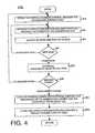
- FIG. 4illustrates a flow diagram of steps performed in accordance with an embodiment of the present invention for generating a memory resident look-up table having row-to-row brightness correction values.
- FIG. 5illustrates a flow diagram of steps performed in accordance with an embodiment of the present invention for display processing using the memory resident look-up table to provide brightness correction in an FED device.
- FIG. 6is a logical block diagram of display circuitry used in accordance with one embodiment of the present invention that provides camouflaged brightness correction by introducing a high frequency noise signal.
- FIG. 7is a flow diagram of steps performed in accordance with an embodiment of the present invention for performing camouflaged brightness correction by introducing a high frequency noise signal during display processing.
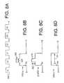
- FIG. 8Aillustrates normal, uncorrected, row on-time pulses for a series of sequential rows.
- FIG. 8B, FIG. 8 C and FIG. 8Dillustrate three embodiments of the present invention for providing row on-time pulse adjustment and shaping to provide row-to-row brightness correction.
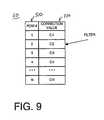
- FIG. 9is a memory resident look-up table containing brightness correction values having one respective correction value for each row.
- FIG. 10is a graph of current versus row number illustrating an uncorrected brightness profile for an FED device and a corrected profile in accordance with an embodiment of the present invention.
- FIG. 11is a flow diagram illustrating steps of a process in accordance with an embodiment of the present invention for using cathode burn-in processes to correct for row-to-row brightness variations within an FED device.
- FIG. 1illustrates a cross section of an exemplary field emission display (FED) device 100 a .
- the FED device 100 acontains a high voltage faceplate or anode 20 having phosphor spots thereon.
- Spacer walls 30are disposed between the anode 20 and rows/columns of emitters 40 .
- the spacer walls 30provide structural integrity for the device 100 a under the tube's vacuum pressure.
- FED technology relating to device 100 ais described in more detail in the following US Patents which are hereby incorporated by reference: U.S. Pat. No. 6,037,918 (application Ser. No. 09/050,664); U.S. Pat. No. 6,051,937 (application Ser. No.
- the emitters 40 of FIG. 1are electron emissive elements.
- One type of electron-emissive element 40is described in U.S. Pat. No. 5,608,283, issued on Mar. 4, 1997 to Twichell et al., and another type is described in U.S. Pat. No. 5,607,335, issued on Mar. 4, 1997 to Spindt et al., which are both incorporated herein by reference.
- the tip of the electron-emissive elementis exposed through a corresponding opening in a gate electrode.
- the above FED configuration 100 ais also described in more detail in the following United States Patents: U.S. Pat. No. 5,541,473 issued on Jul. 30, 1996 to Duboc, Jr. et al.; U.S. Pat. No.
- the spacer walls 30introduce brightness variations from row-to-row in the FED device.
- Several embodiments of the present inventionare described below for compensating for these variations to produce a better displayed image that is free of discernible brightness artifacts caused by the presence of the spacer walls or for other reasons.
- FIG. 2illustrates a FED device 100 b having a memory resident look-up table 60 for providing brightness corrections for row-to-row variations.
- the table 60stores a respective brightness correction value for each row of the FED device.
- a correction circuit 70During a particular row's on-time, its on-time pulse is modified by a correction circuit 70 to produce a corrected on-time pulse 420 that is emitted from the row driver.
- the correction performed by correction circuit 70is based on a correction value supplied by table 60 that is customized for the particular row.
- a synchronizer circuit 95generates the appropriate frame update signals in accordance with well known technology.
- correctionmay be applied by changing the column voltages instead of changing the row voltages, but still synchronized with the row number.
- the respective brightness correction valuesare determined based on accurate electronic measurements also made by device 100 b in accordance with embodiments of the present invention. While a row is being driven, row brightness is proportional to the current drawn by the anode 20 . Therefore, circuit 85 measures the current received by the faceplate or anode 20 in coincidence with a given row being driven. Current of the row can thereby be determined and related to row brightness for each row.
- FIG. 4illustrates a flow diagram describing the general measurement process 200 .
- FIG. 3 A and FIG. 3Billustrate timing diagrams of an exemplary implementation. It is assumed that during current measurement, a uniform pattern is displayed on the FED device, e.g., an all-white pattern may be used.
- the background current drawn through the anode 20is measured during the vertical blanking interval of a display frame (shown as signal 122 of FIG. 3 A and FIG. 3B) and saved.
- a row, e.g., the ith row, of the displayis driven and simultaneously the current drawn by the anode 20 is measured by circuit 85 . Any number of well known currents measuring circuits can be used for circuit 85 and furthermore circuit 85 may contain an isolator circuit due the high voltage applied to the anode 20 .
- a settling timeis allowed for the current associated with the ith row to completely decay and be measured. Current measuring continues (for the ith row) through the settling time for each row. After the settling time 215 , if more rows need to be measured in the frame, then a next row is selected and processing returns to step 210 . If the frame is done, then step 225 determines the RC decay function associated with the current drawn by the last row of the frame. This is done to determine the current “spill over” amount from one row to another. If another frame worth of measurement is required, then step 205 is entered. It is appreciated that all the measurements taken for a given frame are averaged over multiple frames for increased accuracy.
- Measurementmay also be performed by alternating between measuring even and odd rows.
- process 200then computes the average measured current for each row of the FED device. Subtracted from these values is the average of the background current value measured by step 205 . Additionally, the average of the spill over amount (as determined by step 225 ) is also subtracted out of each measured row current value. The values for each row are then compared to a brightness standard and the differences there between are stored in a memory resident look-up table at step 240 and indexed by row number. Alternatively, the measured current amounts can be directly stored. Typically, frames are processed at 30 Hz and 1-20 seconds worth of measurement leads to an error of less than 1 percent on the current measurements described herein.
- FIG. 3 A and FIG. 3Billustrate one implementation of process 200 in accordance with an embodiment of the present invention.
- odd rowsare first driven with even rows not being driven but nevertheless given their allotments of time.
- the timing diagram 120 arepresents a progressive scan from rows 1 to n.
- the vertical blanking period 122is shown and background current through the anode is measured during this period. It is appreciated that the period of time allotted for each even row supplies the settling time for the odd rows, as shown by row2, row4 and row6, for instance.
- Pulse 130 ( 1 )illustrates the current measured at the anode 20 in response to row1 being driven.
- a decay of currentfollows through the settling time allotted for row2 (which is not driven).
- the present inventionadditionally measures this decay current for row1.
- a small tail 142actually leads into the timing for row3. This is the spill over 142 amount for row1.
- the RC decay of the last driven row, row n ⁇ 1is measured as shown by pulse 130 ( n ⁇ 1 ). This measurement allows the spill over or tail 142 amount to be determined and then it can be subtracted from each row. The current values for each odd row are then reduced by the measured tail amount and also by the background current amount. From frame to frame, the measured values are averaged for increased accuracy.
- FIG. 3Billustrates a timing diagram 120 b for the measurement of the even rows with the odd rows not driven but used as settling time periods. Again, the background current is measured during the vertical blanking period 122 and then the current is measured in each even row. The last row, n, is then measured for its RC decay. Like the odd rows, the current is measured for the even rows, and averaged over a number of frames. The results for all measured rows are then stored in the memory resident look-up table.
- the values stored in the memory resident look-up tablecan be used to adjust the maximum row on-time voltage pulse to eliminate variations in brightness from row-to-row. This can be done for all rows.
- the row correction circuitry as shown in FIG. 2can be applied solely to the rows adjacent to the spacer walls. As described more fully below, in lieu of adjusting the row on-time pulse voltage, the period of the row on-time could also be adjusted to provide row-to-row brightness balancing.
- FIG. 5illustrates a display process 300 that makes use of the memory resident correction table to provide brightness balancing row-to-row.
- a progressive scanis contemplated and rows 1 to n are sequentially driven to display a frame.
- the ith rowis to be driven, and the correction value for the ith row is then obtained from the memory resident correction table using the row number as an index.
- This valueis then applied, at step 310 , to adjust the row on-time pulse for the ith row. Either amplitude or pulse width modulation can be performed.
- the corrected row on-time pulseis then used to drive the ith row at step 315 . If this is not the last row of the frame, then step 305 is entered for the next row. It is appreciated that either progressive or interlaced scan can be used.
- step 325is entered where the appropriate frame control signals are reset to allow vertical blanking, etc. If more frames are required, then step 305 is entered again.
- FIG. 6illustrates another embodiment of the present invention for providing row-to-row brightness balancing.
- This embodiment 100 cintroduces a small amount of noise to each row in order to “camouflage” any brightness variations that occur from row-to-row.
- the row voltage amplitudeis modulated to introduce the noise amount.
- the introduction of high frequency noisecan be performed in combination with other brightness correction techniques described herein.
- Embodiment 100 cis analogous to embodiment 100 b (FIG. 2) except for the introduction of high frequency noise generation circuit 65 , which generates a high frequency noise signal 340 .
- This noise signal 340may be periodic in nature and is fed to the correction circuit 70 .
- the correction table 60may also be used.
- the noise signal 340is introduced by the correction circuit 70 to slightly alter the row on-time pulses in a pseudo random way.
- the noise signalis adjusted to a level that helps to camouflage any row-to-row brightness variations (e.g., eliminate perceived row brightness variations) but yet does not cause any perceptible image degradation or artifacts over the area of the display screen.
- Circuit 65may be an electronic oscillator circuit having a fixed frequency.
- FIG. 7illustrates a display process 350 utilizing the embodiment 100 c of FIG. 6 .
- the high frequency noise signalis obtained and at step 360 it is applied to the row on-time pulse for an ith row of a frame.
- a progressive or interlaced scanmay be performed.
- a correction value from the memory resident correction table 60may also be introduced to the row's on-time pulse.
- the corrected row on-time pulseis then used to drive the ith row.
- step 355is entered for the next row. If the frame is complete, then step 375 is entered where the appropriate frame control signals are reset to allow vertical blanking, etc. If more frames are required, then step 355 is entered again.
- FIG. 8Aillustrates a set of uncorrected row on-time pulses 410 .
- a small pulse(correction pulse, top hat pulse) of fixed amplitude, is added to the amplitude of the row on-time pulse in order to provide brightness control.
- FIG. 8Billustrates an embodiment wherein the correction pulse 430 is added, by the correction circuit 70 , to an uncorrected row on-time pulse 410 to create a composite or corrected pulse 420 ( a ).
- the pulse width 435 of the correction pulse 430is varied depending on the correction value from the memory resident correction table.
- the correction pulse 430may be placed in any location (e.g., right or left) with respect to the uncorrected row on-time pulse 410 , and as shown in FIG. 8B, the pulse is generally located in the middle of the uncorrected pulse 410 in a preferred embodiment.
- FIG. 8Cillustrates that in another embodiment of the present invention, the pulse width of the correction pulse 430 remains constant, but its amplitude 455 is varied depending on the brightness correction required as indicated by the correction value from the memory resident correction table.
- the composite signal pulse 420 ( b )is shown. If brightness needs to be increased for an ith row, then the amplitude of the correction pulse 430 is increased by the correction circuit 70 . Conversely, if brightness needs to be decreased for an ith row, then the amplitude of the correction pulse 430 is decreased by the correction circuit 70 .
- the correction pulse 430may be placed in any location (e.g., right or left) with respect to the uncorrected row on-time pulse 410 , and as shown in FIG. 8C, the pulse is generally located in the middle of the uncorrected pulse 410 in a preferred embodiment.
- both the amplitude 445 and the pulse width 435 of the correction pulse 430may be altered based on the correction value stored in the memory resident correction table for a given row.
- FIG. 8Dillustrates that in another embodiment of the present invention, the pulse width 450 of the uncorrected row on-time pulse is varied by the correction circuit 70 depending on the brightness correction required as indicated by the correction value from the memory resident correction table. No top hat pulse is used.
- the amplitude of the row on-time pulsemay also be varied depending on the brightness correction required as indicated by the correction value from the memory resident correction table. Again, no top hat pulse is used
- step 240may be modified so that the high pass filter 620 (see FIG. 10) is applied to the measured current values and the difference between the two are stored as correction values in the memory correction table.
- FIG. 9illustrates an exemplary memory resident correction table 60 in accordance with an embodiment of the present invention.
- a separate correction value 520is provided for each row of the display.
- the correction valuesmay be stored digitally and may be indexed by the row number.
- FIG. 10illustrates a graph of current along the vertical and row number along the horizontal.
- Graph 615represents the current measurements of the n rows taken using the methods described herein. The current measurements illustrate that a general trend of current fall off from row 1 to row n exists. This illustrates that the overall brightness of the FED display gradually varies from brighter to dimmer from the top to the bottom across the face of FED display. Generally, large brightness trends that are gradual from the top to the bottom of the display are not perceptible by the human eye. However, large brightness changes from row-to-row are very perceptible and vivid to the human eye.
- a filter 620e.g., a high pass filter
- the filter 620provides good row-to-row localized brightness normalization.
- the filter 620also better matches the eye's sensitivity and eliminates large variations between rows that are close to each other, but does not attempt to correct the overall trend of the current profile (most often called “fade”).
- the present inventionapplies a filter 620 (e.g., a high pass filtered correction table) to adjust or correct regional row brightness variations rather than forcing each brightness value to a predetermined fixed amount 630 .
- a filter 620e.g., a high pass filtered correction table
- Thisprovides localized or regional brightness normalization while allowing a general and imperceptible brightness trend to exist across the face of the FED display.
- One embodiment of the present inventionapplies a correction of low range (e.g., the small up and down arrows) which provides localized row-to-row brightness normalization.
- the low range correctionrequires less memory as the correction values are smaller than they would be if each row was forced to some fixed brightness amount 630 , as is shown by the graphs of FIG. 10 . Therefore, what is stored in the correction table 60 , for each row, are the differences between the uncorrected graph 615 and the corrected graph 620 in accordance with one embodiments of the present invention.
- the embodiment described with respect to FIG. 11is a method for physically altering the emitters of the FED to correct for brightness variations row-to-row.
- a mapcan be generated of the current profile of the cathode before and during burn-in.
- display patternscan be applied that vary the amount of time each row is on to reduce or eliminate the cathode current variations from row-to-row or regionally reduce or eliminate them. Because there is significant change in the operating voltage during the initial cathode burn in, the emission current can be significantly changed by sending a non uniform data pattern to the column drivers during this initial stage.
- FIG. 11illustrates a process 710 regarding this embodiment of the present invention.
- the brightness of each rowis measured.
- the brightnessmay be measured using the electronic current measurement methods described herein.
- the brightnessmay be optically measured by presenting the FED display with an optical measuring device which directly measures the relative brightness of each row.
- a data profileis recorded that includes a brightness value for each row.
- a deviation from a norm or a filtermay be recorded for each row.
- the measured data profile obtained from step 710is used to varying the cathode burn-in process in order to correct for the brightness variations.
- the physical properties of the emitterscan be altered during burn-in to make rows dimmer or brighter, as the case requires.
- the work function of the emittermay be altered.
- the shape and size of the emitter tipmay be altered.
- the chemical composition of the emitter tipmay be altered during cathode burn-in.
- row-to-row variationscan be performed to vary the brightness of individual rows.
- row specific display patternsmay be used that are targeted to the brightness variations detected in step 710 .
- Just driving a row during cathode burn-in for predetermined time periodsmay alter its brightness.
- Gasmay also be applied to alter the brightness of a row. For instance, driving a row in the presence of oxygen may make the row dimmer. Alternatively, driving a row in the presence of methane may make the row brighter.
- step 725is entered.
- Step 715is repeated such multiple measurements and adjustments may be performed to more refine the brightness normalization.
- step 725if a threshold matching amount is reached, then process 710 exists.
Landscapes
- Engineering & Computer Science (AREA)
- Physics & Mathematics (AREA)
- Computer Hardware Design (AREA)
- General Physics & Mathematics (AREA)
- Theoretical Computer Science (AREA)
- Manufacturing & Machinery (AREA)
- Control Of Indicators Other Than Cathode Ray Tubes (AREA)
- Cathode-Ray Tubes And Fluorescent Screens For Display (AREA)
- Closed-Circuit Television Systems (AREA)
- Indicating Measured Values (AREA)
- Measuring Pulse, Heart Rate, Blood Pressure Or Blood Flow (AREA)
- Investigating Or Analysing Materials By The Use Of Chemical Reactions (AREA)
Abstract
Description
Claims (8)
Priority Applications (13)
| Application Number | Priority Date | Filing Date | Title |
|---|---|---|---|
| US09/895,985US6822628B2 (en) | 2001-06-28 | 2001-06-28 | Methods and systems for compensating row-to-row brightness variations of a field emission display |
| KR1020037017053AKR100879249B1 (en) | 2001-06-28 | 2002-06-24 | Method and system for measuring display characteristics of FED |
| EP02749666AEP1402506B1 (en) | 2001-06-28 | 2002-06-24 | Method and system for row-by-row brightness correction in an FED |
| EP09011212AEP2131345A3 (en) | 2001-06-28 | 2002-06-24 | Method and system for measuring display attributes of a fed |
| DE60236282TDE60236282D1 (en) | 2001-06-28 | 2002-06-24 | Method and device for line-by-line brightness correction in a FED |
| KR1020087018121AKR100906343B1 (en) | 2001-06-28 | 2002-06-24 | Methods and systems for measuring display attributes of a fed |
| AU2002320162AAU2002320162A1 (en) | 2001-06-28 | 2002-06-24 | Methods and systems for measuring display attributes of a fed |
| PCT/US2002/020243WO2003002957A2 (en) | 2001-06-28 | 2002-06-24 | Methods and systems for measuring display attributes of a fed |
| AT02749666TATE467205T1 (en) | 2001-06-28 | 2002-06-24 | METHOD AND DEVICE FOR LINE-BY-LINE BRIGHTNESS CORRECTION IN A FED |
| JP2003508895AJP4546080B2 (en) | 2001-06-28 | 2002-06-24 | Driving method of field emission display device |
| TW091114178ATW582008B (en) | 2001-06-28 | 2002-06-27 | Methods and systems for measuring display attributes of a FED |
| MYPI20022470AMY131950A (en) | 2001-06-28 | 2002-06-28 | Methods and systems for compensating row-to-row brightness variations of a field emission display |
| US10/969,494US7403175B1 (en) | 2001-06-28 | 2004-10-19 | Methods and systems for compensating row-to-row brightness variations of a field emission display |
Applications Claiming Priority (1)
| Application Number | Priority Date | Filing Date | Title |
|---|---|---|---|
| US09/895,985US6822628B2 (en) | 2001-06-28 | 2001-06-28 | Methods and systems for compensating row-to-row brightness variations of a field emission display |
Related Child Applications (1)
| Application Number | Title | Priority Date | Filing Date |
|---|---|---|---|
| US10/969,494DivisionUS7403175B1 (en) | 2001-06-28 | 2004-10-19 | Methods and systems for compensating row-to-row brightness variations of a field emission display |
Publications (2)
| Publication Number | Publication Date |
|---|---|
| US20030011537A1 US20030011537A1 (en) | 2003-01-16 |
| US6822628B2true US6822628B2 (en) | 2004-11-23 |
Family
ID=25405412
Family Applications (2)
| Application Number | Title | Priority Date | Filing Date |
|---|---|---|---|
| US09/895,985Expired - Fee RelatedUS6822628B2 (en) | 2001-06-28 | 2001-06-28 | Methods and systems for compensating row-to-row brightness variations of a field emission display |
| US10/969,494Expired - Fee RelatedUS7403175B1 (en) | 2001-06-28 | 2004-10-19 | Methods and systems for compensating row-to-row brightness variations of a field emission display |
Family Applications After (1)
| Application Number | Title | Priority Date | Filing Date |
|---|---|---|---|
| US10/969,494Expired - Fee RelatedUS7403175B1 (en) | 2001-06-28 | 2004-10-19 | Methods and systems for compensating row-to-row brightness variations of a field emission display |
Country Status (10)
| Country | Link |
|---|---|
| US (2) | US6822628B2 (en) |
| EP (2) | EP2131345A3 (en) |
| JP (1) | JP4546080B2 (en) |
| KR (2) | KR100906343B1 (en) |
| AT (1) | ATE467205T1 (en) |
| AU (1) | AU2002320162A1 (en) |
| DE (1) | DE60236282D1 (en) |
| MY (1) | MY131950A (en) |
| TW (1) | TW582008B (en) |
| WO (1) | WO2003002957A2 (en) |
Cited By (166)
| Publication number | Priority date | Publication date | Assignee | Title |
|---|---|---|---|---|
| US20030201954A1 (en)* | 2002-04-26 | 2003-10-30 | Hansen Ronald L. | System and method for recalibrating flat panel field emission displays |
| US20040041977A1 (en)* | 2002-08-26 | 2004-03-04 | Chien-Ching Shen | Method and device for repairing defective pixels of a liquid crystal display panel |
| US7012732B2 (en) | 1994-05-05 | 2006-03-14 | Idc, Llc | Method and device for modulating light with a time-varying signal |
| US7012726B1 (en) | 2003-11-03 | 2006-03-14 | Idc, Llc | MEMS devices with unreleased thin film components |
| US20060066603A1 (en)* | 2004-09-30 | 2006-03-30 | Kabushiki Kaisha Toshiba | Display device and display method |
| US7042643B2 (en) | 1994-05-05 | 2006-05-09 | Idc, Llc | Interferometric modulation of radiation |
| US7060895B2 (en) | 2004-05-04 | 2006-06-13 | Idc, Llc | Modifying the electro-mechanical behavior of devices |
| US20060132394A1 (en)* | 2004-12-17 | 2006-06-22 | Canon Kabushiki Kaisha | Image display apparatus and television apparatus |
| US7110158B2 (en) | 1999-10-05 | 2006-09-19 | Idc, Llc | Photonic MEMS and structures |
| US7119945B2 (en) | 2004-03-03 | 2006-10-10 | Idc, Llc | Altering temporal response of microelectromechanical elements |
| US7123216B1 (en) | 1994-05-05 | 2006-10-17 | Idc, Llc | Photonic MEMS and structures |
| US7130104B2 (en) | 2004-09-27 | 2006-10-31 | Idc, Llc | Methods and devices for inhibiting tilting of a mirror in an interferometric modulator |
| US7136213B2 (en) | 2004-09-27 | 2006-11-14 | Idc, Llc | Interferometric modulators having charge persistence |
| US7138984B1 (en) | 2001-06-05 | 2006-11-21 | Idc, Llc | Directly laminated touch sensitive screen |
| US7142346B2 (en) | 2003-12-09 | 2006-11-28 | Idc, Llc | System and method for addressing a MEMS display |
| US20060290618A1 (en)* | 2003-09-05 | 2006-12-28 | Masaharu Goto | Display panel conversion data deciding method and measuring apparatus |
| US7161728B2 (en) | 2003-12-09 | 2007-01-09 | Idc, Llc | Area array modulation and lead reduction in interferometric modulators |
| US7161730B2 (en) | 2004-09-27 | 2007-01-09 | Idc, Llc | System and method for providing thermal compensation for an interferometric modulator display |
| US7164520B2 (en) | 2004-05-12 | 2007-01-16 | Idc, Llc | Packaging for an interferometric modulator |
| US7172915B2 (en) | 2003-01-29 | 2007-02-06 | Qualcomm Mems Technologies Co., Ltd. | Optical-interference type display panel and method for making the same |
| US7193768B2 (en) | 2003-08-26 | 2007-03-20 | Qualcomm Mems Technologies, Inc. | Interference display cell |
| US7198973B2 (en) | 2003-04-21 | 2007-04-03 | Qualcomm Mems Technologies, Inc. | Method for fabricating an interference display unit |
| US7221495B2 (en) | 2003-06-24 | 2007-05-22 | Idc Llc | Thin film precursor stack for MEMS manufacturing |
| US7250315B2 (en) | 2002-02-12 | 2007-07-31 | Idc, Llc | Method for fabricating a structure for a microelectromechanical system (MEMS) device |
| US7256922B2 (en) | 2004-07-02 | 2007-08-14 | Idc, Llc | Interferometric modulators with thin film transistors |
| US7259449B2 (en) | 2004-09-27 | 2007-08-21 | Idc, Llc | Method and system for sealing a substrate |
| US7259865B2 (en) | 2004-09-27 | 2007-08-21 | Idc, Llc | Process control monitors for interferometric modulators |
| US7289256B2 (en) | 2004-09-27 | 2007-10-30 | Idc, Llc | Electrical characterization of interferometric modulators |
| US7289259B2 (en) | 2004-09-27 | 2007-10-30 | Idc, Llc | Conductive bus structure for interferometric modulator array |
| US7291921B2 (en) | 2003-09-30 | 2007-11-06 | Qualcomm Mems Technologies, Inc. | Structure of a micro electro mechanical system and the manufacturing method thereof |
| US7297471B1 (en) | 2003-04-15 | 2007-11-20 | Idc, Llc | Method for manufacturing an array of interferometric modulators |
| US7299681B2 (en) | 2004-09-27 | 2007-11-27 | Idc, Llc | Method and system for detecting leak in electronic devices |
| US7302157B2 (en) | 2004-09-27 | 2007-11-27 | Idc, Llc | System and method for multi-level brightness in interferometric modulation |
| US7304784B2 (en) | 2004-09-27 | 2007-12-04 | Idc, Llc | Reflective display device having viewable display on both sides |
| US7310179B2 (en) | 2004-09-27 | 2007-12-18 | Idc, Llc | Method and device for selective adjustment of hysteresis window |
| US7317568B2 (en) | 2004-09-27 | 2008-01-08 | Idc, Llc | System and method of implementation of interferometric modulators for display mirrors |
| US7321457B2 (en) | 2006-06-01 | 2008-01-22 | Qualcomm Incorporated | Process and structure for fabrication of MEMS device having isolated edge posts |
| US7321456B2 (en) | 2004-09-27 | 2008-01-22 | Idc, Llc | Method and device for corner interferometric modulation |
| US7327510B2 (en) | 2004-09-27 | 2008-02-05 | Idc, Llc | Process for modifying offset voltage characteristics of an interferometric modulator |
| US7343080B2 (en) | 2004-09-27 | 2008-03-11 | Idc, Llc | System and method of testing humidity in a sealed MEMS device |
| US7345805B2 (en) | 2004-09-27 | 2008-03-18 | Idc, Llc | Interferometric modulator array with integrated MEMS electrical switches |
| US7349139B2 (en) | 2004-09-27 | 2008-03-25 | Idc, Llc | System and method of illuminating interferometric modulators using backlighting |
| US7349136B2 (en) | 2004-09-27 | 2008-03-25 | Idc, Llc | Method and device for a display having transparent components integrated therein |
| US7355779B2 (en) | 2005-09-02 | 2008-04-08 | Idc, Llc | Method and system for driving MEMS display elements |
| US7359066B2 (en) | 2004-09-27 | 2008-04-15 | Idc, Llc | Electro-optical measurement of hysteresis in interferometric modulators |
| US7368803B2 (en) | 2004-09-27 | 2008-05-06 | Idc, Llc | System and method for protecting microelectromechanical systems array using back-plate with non-flat portion |
| US7369296B2 (en) | 2004-09-27 | 2008-05-06 | Idc, Llc | Device and method for modifying actuation voltage thresholds of a deformable membrane in an interferometric modulator |
| US7369292B2 (en) | 2006-05-03 | 2008-05-06 | Qualcomm Mems Technologies, Inc. | Electrode and interconnect materials for MEMS devices |
| US7369294B2 (en) | 2004-09-27 | 2008-05-06 | Idc, Llc | Ornamental display device |
| US7373026B2 (en) | 2004-09-27 | 2008-05-13 | Idc, Llc | MEMS device fabricated on a pre-patterned substrate |
| US7372613B2 (en) | 2004-09-27 | 2008-05-13 | Idc, Llc | Method and device for multistate interferometric light modulation |
| US7382515B2 (en) | 2006-01-18 | 2008-06-03 | Qualcomm Mems Technologies, Inc. | Silicon-rich silicon nitrides as etch stops in MEMS manufacture |
| US7385744B2 (en) | 2006-06-28 | 2008-06-10 | Qualcomm Mems Technologies, Inc. | Support structure for free-standing MEMS device and methods for forming the same |
| US7388704B2 (en) | 2006-06-30 | 2008-06-17 | Qualcomm Mems Technologies, Inc. | Determination of interferometric modulator mirror curvature and airgap variation using digital photographs |
| USRE40436E1 (en)* | 2001-08-01 | 2008-07-15 | Idc, Llc | Hermetic seal and method to create the same |
| US7403175B1 (en) | 2001-06-28 | 2008-07-22 | Canon Kabushiki Kaisha | Methods and systems for compensating row-to-row brightness variations of a field emission display |
| US7405924B2 (en) | 2004-09-27 | 2008-07-29 | Idc, Llc | System and method for protecting microelectromechanical systems array using structurally reinforced back-plate |
| US7405863B2 (en) | 2006-06-01 | 2008-07-29 | Qualcomm Mems Technologies, Inc. | Patterning of mechanical layer in MEMS to reduce stresses at supports |
| US7405861B2 (en) | 2004-09-27 | 2008-07-29 | Idc, Llc | Method and device for protecting interferometric modulators from electrostatic discharge |
| US7415186B2 (en) | 2004-09-27 | 2008-08-19 | Idc, Llc | Methods for visually inspecting interferometric modulators for defects |
| US7417783B2 (en) | 2004-09-27 | 2008-08-26 | Idc, Llc | Mirror and mirror layer for optical modulator and method |
| US7417735B2 (en) | 2004-09-27 | 2008-08-26 | Idc, Llc | Systems and methods for measuring color and contrast in specular reflective devices |
| US7417784B2 (en) | 2006-04-19 | 2008-08-26 | Qualcomm Mems Technologies, Inc. | Microelectromechanical device and method utilizing a porous surface |
| US7420728B2 (en) | 2004-09-27 | 2008-09-02 | Idc, Llc | Methods of fabricating interferometric modulators by selectively removing a material |
| US7420725B2 (en) | 2004-09-27 | 2008-09-02 | Idc, Llc | Device having a conductive light absorbing mask and method for fabricating same |
| US7424198B2 (en) | 2004-09-27 | 2008-09-09 | Idc, Llc | Method and device for packaging a substrate |
| US7446927B2 (en) | 2004-09-27 | 2008-11-04 | Idc, Llc | MEMS switch with set and latch electrodes |
| US7450295B2 (en) | 2006-03-02 | 2008-11-11 | Qualcomm Mems Technologies, Inc. | Methods for producing MEMS with protective coatings using multi-component sacrificial layers |
| US7453579B2 (en) | 2004-09-27 | 2008-11-18 | Idc, Llc | Measurement of the dynamic characteristics of interferometric modulators |
| US7460291B2 (en) | 1994-05-05 | 2008-12-02 | Idc, Llc | Separable modulator |
| US7460246B2 (en) | 2004-09-27 | 2008-12-02 | Idc, Llc | Method and system for sensing light using interferometric elements |
| US7471444B2 (en) | 1996-12-19 | 2008-12-30 | Idc, Llc | Interferometric modulation of radiation |
| US7471442B2 (en) | 2006-06-15 | 2008-12-30 | Qualcomm Mems Technologies, Inc. | Method and apparatus for low range bit depth enhancements for MEMS display architectures |
| US7476327B2 (en) | 2004-05-04 | 2009-01-13 | Idc, Llc | Method of manufacture for microelectromechanical devices |
| US7486429B2 (en) | 2004-09-27 | 2009-02-03 | Idc, Llc | Method and device for multistate interferometric light modulation |
| US7492502B2 (en) | 2004-09-27 | 2009-02-17 | Idc, Llc | Method of fabricating a free-standing microstructure |
| US7499208B2 (en) | 2004-08-27 | 2009-03-03 | Udc, Llc | Current mode display driver circuit realization feature |
| US7515147B2 (en) | 2004-08-27 | 2009-04-07 | Idc, Llc | Staggered column drive circuit systems and methods |
| US7527996B2 (en) | 2006-04-19 | 2009-05-05 | Qualcomm Mems Technologies, Inc. | Non-planar surface structures and process for microelectromechanical systems |
| US7527995B2 (en) | 2004-09-27 | 2009-05-05 | Qualcomm Mems Technologies, Inc. | Method of making prestructure for MEMS systems |
| US7527998B2 (en) | 2006-06-30 | 2009-05-05 | Qualcomm Mems Technologies, Inc. | Method of manufacturing MEMS devices providing air gap control |
| US7532377B2 (en) | 1998-04-08 | 2009-05-12 | Idc, Llc | Movable micro-electromechanical device |
| US7532195B2 (en) | 2004-09-27 | 2009-05-12 | Idc, Llc | Method and system for reducing power consumption in a display |
| US7532194B2 (en) | 2004-02-03 | 2009-05-12 | Idc, Llc | Driver voltage adjuster |
| US7534640B2 (en) | 2005-07-22 | 2009-05-19 | Qualcomm Mems Technologies, Inc. | Support structure for MEMS device and methods therefor |
| US7535466B2 (en) | 2004-09-27 | 2009-05-19 | Idc, Llc | System with server based control of client device display features |
| US7545550B2 (en) | 2004-09-27 | 2009-06-09 | Idc, Llc | Systems and methods of actuating MEMS display elements |
| US7547565B2 (en) | 2005-02-04 | 2009-06-16 | Qualcomm Mems Technologies, Inc. | Method of manufacturing optical interference color display |
| US7547568B2 (en) | 2006-02-22 | 2009-06-16 | Qualcomm Mems Technologies, Inc. | Electrical conditioning of MEMS device and insulating layer thereof |
| US7550794B2 (en) | 2002-09-20 | 2009-06-23 | Idc, Llc | Micromechanical systems device comprising a displaceable electrode and a charge-trapping layer |
| US7550810B2 (en) | 2006-02-23 | 2009-06-23 | Qualcomm Mems Technologies, Inc. | MEMS device having a layer movable at asymmetric rates |
| US7551159B2 (en) | 2004-08-27 | 2009-06-23 | Idc, Llc | System and method of sensing actuation and release voltages of an interferometric modulator |
| US7554711B2 (en) | 1998-04-08 | 2009-06-30 | Idc, Llc. | MEMS devices with stiction bumps |
| US7553684B2 (en) | 2004-09-27 | 2009-06-30 | Idc, Llc | Method of fabricating interferometric devices using lift-off processing techniques |
| US7554714B2 (en) | 2004-09-27 | 2009-06-30 | Idc, Llc | Device and method for manipulation of thermal response in a modulator |
| US7560299B2 (en) | 2004-08-27 | 2009-07-14 | Idc, Llc | Systems and methods of actuating MEMS display elements |
| US7564612B2 (en) | 2004-09-27 | 2009-07-21 | Idc, Llc | Photonic MEMS and structures |
| US7566664B2 (en) | 2006-08-02 | 2009-07-28 | Qualcomm Mems Technologies, Inc. | Selective etching of MEMS using gaseous halides and reactive co-etchants |
| US7567373B2 (en) | 2004-07-29 | 2009-07-28 | Idc, Llc | System and method for micro-electromechanical operation of an interferometric modulator |
| US7582952B2 (en) | 2006-02-21 | 2009-09-01 | Qualcomm Mems Technologies, Inc. | Method for providing and removing discharging interconnect for chip-on-glass output leads and structures thereof |
| US7586484B2 (en) | 2004-09-27 | 2009-09-08 | Idc, Llc | Controller and driver features for bi-stable display |
| US7602375B2 (en) | 2004-09-27 | 2009-10-13 | Idc, Llc | Method and system for writing data to MEMS display elements |
| US7623287B2 (en) | 2006-04-19 | 2009-11-24 | Qualcomm Mems Technologies, Inc. | Non-planar surface structures and process for microelectromechanical systems |
| US7626581B2 (en) | 2004-09-27 | 2009-12-01 | Idc, Llc | Device and method for display memory using manipulation of mechanical response |
| US7630114B2 (en) | 2005-10-28 | 2009-12-08 | Idc, Llc | Diffusion barrier layer for MEMS devices |
| US7630119B2 (en) | 2004-09-27 | 2009-12-08 | Qualcomm Mems Technologies, Inc. | Apparatus and method for reducing slippage between structures in an interferometric modulator |
| US7636151B2 (en) | 2006-01-06 | 2009-12-22 | Qualcomm Mems Technologies, Inc. | System and method for providing residual stress test structures |
| US7643203B2 (en) | 2006-04-10 | 2010-01-05 | Qualcomm Mems Technologies, Inc. | Interferometric optical display system with broadband characteristics |
| US7649671B2 (en) | 2006-06-01 | 2010-01-19 | Qualcomm Mems Technologies, Inc. | Analog interferometric modulator device with electrostatic actuation and release |
| US7653371B2 (en) | 2004-09-27 | 2010-01-26 | Qualcomm Mems Technologies, Inc. | Selectable capacitance circuit |
| US7668415B2 (en) | 2004-09-27 | 2010-02-23 | Qualcomm Mems Technologies, Inc. | Method and device for providing electronic circuitry on a backplate |
| US7675669B2 (en) | 2004-09-27 | 2010-03-09 | Qualcomm Mems Technologies, Inc. | Method and system for driving interferometric modulators |
| US7679627B2 (en) | 2004-09-27 | 2010-03-16 | Qualcomm Mems Technologies, Inc. | Controller and driver features for bi-stable display |
| US7684104B2 (en) | 2004-09-27 | 2010-03-23 | Idc, Llc | MEMS using filler material and method |
| US7692839B2 (en) | 2004-09-27 | 2010-04-06 | Qualcomm Mems Technologies, Inc. | System and method of providing MEMS device with anti-stiction coating |
| US7701631B2 (en) | 2004-09-27 | 2010-04-20 | Qualcomm Mems Technologies, Inc. | Device having patterned spacers for backplates and method of making the same |
| US7702192B2 (en) | 2006-06-21 | 2010-04-20 | Qualcomm Mems Technologies, Inc. | Systems and methods for driving MEMS display |
| US7706044B2 (en) | 2003-05-26 | 2010-04-27 | Qualcomm Mems Technologies, Inc. | Optical interference display cell and method of making the same |
| US7706050B2 (en) | 2004-03-05 | 2010-04-27 | Qualcomm Mems Technologies, Inc. | Integrated modulator illumination |
| US7710629B2 (en) | 2004-09-27 | 2010-05-04 | Qualcomm Mems Technologies, Inc. | System and method for display device with reinforcing substance |
| US7710632B2 (en) | 2004-09-27 | 2010-05-04 | Qualcomm Mems Technologies, Inc. | Display device having an array of spatial light modulators with integrated color filters |
| US7711239B2 (en) | 2006-04-19 | 2010-05-04 | Qualcomm Mems Technologies, Inc. | Microelectromechanical device and method utilizing nanoparticles |
| US7719500B2 (en) | 2004-09-27 | 2010-05-18 | Qualcomm Mems Technologies, Inc. | Reflective display pixels arranged in non-rectangular arrays |
| US7724993B2 (en) | 2004-09-27 | 2010-05-25 | Qualcomm Mems Technologies, Inc. | MEMS switches with deforming membranes |
| US7763546B2 (en) | 2006-08-02 | 2010-07-27 | Qualcomm Mems Technologies, Inc. | Methods for reducing surface charges during the manufacture of microelectromechanical systems devices |
| US20100202038A1 (en)* | 2006-12-20 | 2010-08-12 | Qualcomm Mems Technologies, Inc. | Mems device and interconnects for same |
| US7777715B2 (en) | 2006-06-29 | 2010-08-17 | Qualcomm Mems Technologies, Inc. | Passive circuits for de-multiplexing display inputs |
| US7781850B2 (en) | 2002-09-20 | 2010-08-24 | Qualcomm Mems Technologies, Inc. | Controlling electromechanical behavior of structures within a microelectromechanical systems device |
| US7795061B2 (en) | 2005-12-29 | 2010-09-14 | Qualcomm Mems Technologies, Inc. | Method of creating MEMS device cavities by a non-etching process |
| US7807488B2 (en) | 2004-09-27 | 2010-10-05 | Qualcomm Mems Technologies, Inc. | Display element having filter material diffused in a substrate of the display element |
| US7808703B2 (en) | 2004-09-27 | 2010-10-05 | Qualcomm Mems Technologies, Inc. | System and method for implementation of interferometric modulator displays |
| US7813026B2 (en) | 2004-09-27 | 2010-10-12 | Qualcomm Mems Technologies, Inc. | System and method of reducing color shift in a display |
| US20100265563A1 (en)* | 2005-08-19 | 2010-10-21 | Qualcomm Mems Technologies, Inc. | Electromechanical device configured to minimize stress-related deformation and methods for fabricating same |
| US7835061B2 (en) | 2006-06-28 | 2010-11-16 | Qualcomm Mems Technologies, Inc. | Support structures for free-standing electromechanical devices |
| US7843410B2 (en) | 2004-09-27 | 2010-11-30 | Qualcomm Mems Technologies, Inc. | Method and device for electrically programmable display |
| US7889163B2 (en) | 2004-08-27 | 2011-02-15 | Qualcomm Mems Technologies, Inc. | Drive method for MEMS devices |
| US7893919B2 (en) | 2004-09-27 | 2011-02-22 | Qualcomm Mems Technologies, Inc. | Display region architectures |
| US7903047B2 (en) | 2006-04-17 | 2011-03-08 | Qualcomm Mems Technologies, Inc. | Mode indicator for interferometric modulator displays |
| US7911428B2 (en) | 2004-09-27 | 2011-03-22 | Qualcomm Mems Technologies, Inc. | Method and device for manipulating color in a display |
| US7916103B2 (en) | 2004-09-27 | 2011-03-29 | Qualcomm Mems Technologies, Inc. | System and method for display device with end-of-life phenomena |
| US7916980B2 (en) | 2006-01-13 | 2011-03-29 | Qualcomm Mems Technologies, Inc. | Interconnect structure for MEMS device |
| US7920135B2 (en) | 2004-09-27 | 2011-04-05 | Qualcomm Mems Technologies, Inc. | Method and system for driving a bi-stable display |
| US7920136B2 (en) | 2005-05-05 | 2011-04-05 | Qualcomm Mems Technologies, Inc. | System and method of driving a MEMS display device |
| US7936497B2 (en) | 2004-09-27 | 2011-05-03 | Qualcomm Mems Technologies, Inc. | MEMS device having deformable membrane characterized by mechanical persistence |
| US7948457B2 (en) | 2005-05-05 | 2011-05-24 | Qualcomm Mems Technologies, Inc. | Systems and methods of actuating MEMS display elements |
| US8008736B2 (en) | 2004-09-27 | 2011-08-30 | Qualcomm Mems Technologies, Inc. | Analog interferometric modulator device |
| US8014059B2 (en) | 1994-05-05 | 2011-09-06 | Qualcomm Mems Technologies, Inc. | System and method for charge control in a MEMS device |
| US8049713B2 (en) | 2006-04-24 | 2011-11-01 | Qualcomm Mems Technologies, Inc. | Power consumption optimized display update |
| US8061882B2 (en) | 2006-10-06 | 2011-11-22 | Qualcomm Mems Technologies, Inc. | Illumination device with built-in light coupler |
| US8124434B2 (en) | 2004-09-27 | 2012-02-28 | Qualcomm Mems Technologies, Inc. | Method and system for packaging a display |
| US8174469B2 (en) | 2005-05-05 | 2012-05-08 | Qualcomm Mems Technologies, Inc. | Dynamic driver IC and display panel configuration |
| US8194056B2 (en) | 2006-02-09 | 2012-06-05 | Qualcomm Mems Technologies Inc. | Method and system for writing data to MEMS display elements |
| US8310441B2 (en) | 2004-09-27 | 2012-11-13 | Qualcomm Mems Technologies, Inc. | Method and system for writing data to MEMS display elements |
| US8391630B2 (en) | 2005-12-22 | 2013-03-05 | Qualcomm Mems Technologies, Inc. | System and method for power reduction when decompressing video streams for interferometric modulator displays |
| US20130155085A1 (en)* | 2003-03-10 | 2013-06-20 | Fergason Patent Properties, Llc | Apparatus and method for preparing, storing, transmitting and displaying images |
| US8736590B2 (en) | 2009-03-27 | 2014-05-27 | Qualcomm Mems Technologies, Inc. | Low voltage driver scheme for interferometric modulators |
| US8735225B2 (en) | 2004-09-27 | 2014-05-27 | Qualcomm Mems Technologies, Inc. | Method and system for packaging MEMS devices with glass seal |
| US8817357B2 (en) | 2010-04-09 | 2014-08-26 | Qualcomm Mems Technologies, Inc. | Mechanical layer and methods of forming the same |
| US8830557B2 (en) | 2007-05-11 | 2014-09-09 | Qualcomm Mems Technologies, Inc. | Methods of fabricating MEMS with spacers between plates and devices formed by same |
| US8848294B2 (en) | 2010-05-20 | 2014-09-30 | Qualcomm Mems Technologies, Inc. | Method and structure capable of changing color saturation |
| US8878825B2 (en) | 2004-09-27 | 2014-11-04 | Qualcomm Mems Technologies, Inc. | System and method for providing a variable refresh rate of an interferometric modulator display |
| US8885244B2 (en) | 2004-09-27 | 2014-11-11 | Qualcomm Mems Technologies, Inc. | Display device |
| US8928967B2 (en) | 1998-04-08 | 2015-01-06 | Qualcomm Mems Technologies, Inc. | Method and device for modulating light |
| US8963159B2 (en) | 2011-04-04 | 2015-02-24 | Qualcomm Mems Technologies, Inc. | Pixel via and methods of forming the same |
| US9001412B2 (en) | 2004-09-27 | 2015-04-07 | Qualcomm Mems Technologies, Inc. | Electromechanical device with optical function separated from mechanical and electrical function |
| US9134527B2 (en) | 2011-04-04 | 2015-09-15 | Qualcomm Mems Technologies, Inc. | Pixel via and methods of forming the same |
Families Citing this family (14)
| Publication number | Priority date | Publication date | Assignee | Title |
|---|---|---|---|---|
| JP4047306B2 (en) | 2003-07-15 | 2008-02-13 | キヤノン株式会社 | Correction value determination method and display device manufacturing method |
| JP4194567B2 (en)* | 2004-02-27 | 2008-12-10 | キヤノン株式会社 | Image display device |
| CN100452135C (en)* | 2004-02-27 | 2009-01-14 | 佳能株式会社 | Image display apparatus |
| JP2006047510A (en)* | 2004-08-02 | 2006-02-16 | Oki Electric Ind Co Ltd | Display panel driving circuit and driving method |
| WO2006087327A1 (en)* | 2005-02-16 | 2006-08-24 | Thomson Licensing | Method and apparatus for luminance non-homogeneity compensation in an am-oled |
| JP2007193190A (en) | 2006-01-20 | 2007-08-02 | Sony Corp | Method of driving flat display device |
| US8430188B2 (en) | 2006-12-11 | 2013-04-30 | Vermeer Manufacturing Company | Apparatus for converting a wheeled vehicle to a tracked vehicle |
| WO2008073990A2 (en) | 2006-12-12 | 2008-06-19 | Loegering Mfg. Inc. | Conversion system for a wheeled vehicle |
| KR100863961B1 (en)* | 2007-08-02 | 2008-10-16 | 삼성에스디아이 주식회사 | Light emitting device, display device using same, driving method of light emitting device and driving method of display device |
| EP2048642A1 (en)* | 2007-10-10 | 2009-04-15 | Barco NV | Reducing visibility of display errors |
| US8245800B2 (en) | 2008-12-09 | 2012-08-21 | Vermeer Manufacturing Company | Apparatus for converting a wheeled vehicle to a tracked vehicle |
| KR101479992B1 (en)* | 2008-12-12 | 2015-01-08 | 삼성디스플레이 주식회사 | Method for compensating voltage drop and system therefor and display deivce including the same |
| US11893185B2 (en)* | 2021-09-17 | 2024-02-06 | Apple Inc. | Pixel array and touch array crosstalk mitigation systems and methods |
| TWI820804B (en)* | 2022-07-19 | 2023-11-01 | 大陸商集創北方(珠海)科技有限公司 | Panel fragment detection method, panel fragment detection circuit and OLED display |
Citations (8)
| Publication number | Priority date | Publication date | Assignee | Title |
|---|---|---|---|---|
| US5262698A (en) | 1991-10-31 | 1993-11-16 | Raytheon Company | Compensation for field emission display irregularities |
| US5708451A (en)* | 1995-07-20 | 1998-01-13 | Sgs-Thomson Microelectronics, S.R.L. | Method and device for uniforming luminosity and reducing phosphor degradation of a field emission flat display |
| US6097356A (en)* | 1997-07-01 | 2000-08-01 | Fan; Nongqiang | Methods of improving display uniformity of thin CRT displays by calibrating individual cathode |
| US6140985A (en)* | 1995-06-05 | 2000-10-31 | Canon Kabushiki Kaisha | Image display apparatus |
| US6329759B1 (en)* | 1999-02-17 | 2001-12-11 | Futaba Denshi Kogyo Kabushiki Kaisha | Field emission image display |
| US6392355B1 (en)* | 2000-04-25 | 2002-05-21 | Mcnc | Closed-loop cold cathode current regulator |
| US6462484B2 (en) | 1998-08-31 | 2002-10-08 | Candescent Intellectual Property Services | Procedures and apparatus for turning-on and turning-off elements within a field emission display device |
| US6465966B2 (en)* | 2000-01-24 | 2002-10-15 | Nec Corporation | Field emission display and method of driving the same |
Family Cites Families (28)
| Publication number | Priority date | Publication date | Assignee | Title |
|---|---|---|---|---|
| US651937A (en)* | 1899-05-11 | 1900-06-19 | Leonard S Short | Bag-fastener. |
| US5424605A (en) | 1992-04-10 | 1995-06-13 | Silicon Video Corporation | Self supporting flat video display |
| US5564959A (en) | 1993-09-08 | 1996-10-15 | Silicon Video Corporation | Use of charged-particle tracks in fabricating gated electron-emitting devices |
| US5559389A (en) | 1993-09-08 | 1996-09-24 | Silicon Video Corporation | Electron-emitting devices having variously constituted electron-emissive elements, including cones or pedestals |
| JPH087807A (en)* | 1994-06-27 | 1996-01-12 | Canon Inc | Electron beam irradiation method, electron beam generator, and image forming apparatus using the electron beam generator |
| US5608283A (en) | 1994-06-29 | 1997-03-04 | Candescent Technologies Corporation | Electron-emitting devices utilizing electron-emissive particles which typically contain carbon |
| US5607335A (en) | 1994-06-29 | 1997-03-04 | Silicon Video Corporation | Fabrication of electron-emitting structures using charged-particle tracks and removal of emitter material |
| JP3282411B2 (en)* | 1994-11-04 | 2002-05-13 | 双葉電子工業株式会社 | Driving device for fluorescent display tube |
| US5578899A (en) | 1994-11-21 | 1996-11-26 | Silicon Video Corporation | Field emission device with internal structure for aligning phosphor pixels with corresponding field emitters |
| JP3214328B2 (en)* | 1995-12-28 | 2001-10-02 | 松下電器産業株式会社 | Liquid crystal display |
| US6069597A (en)* | 1997-08-29 | 2000-05-30 | Candescent Technologies Corporation | Circuit and method for controlling the brightness of an FED device |
| US6069598A (en)* | 1997-08-29 | 2000-05-30 | Candescent Technologies Corporation | Circuit and method for controlling the brightness of an FED device in response to a light sensor |
| US6147664A (en) | 1997-08-29 | 2000-11-14 | Candescent Technologies Corporation | Controlling the brightness of an FED device using PWM on the row side and AM on the column side |
| JPH11109913A (en)* | 1997-10-02 | 1999-04-23 | Canon Inc | Image forming method and apparatus |
| US6169529B1 (en) | 1998-03-30 | 2001-01-02 | Candescent Technologies Corporation | Circuit and method for controlling the color balance of a field emission display |
| US6037918A (en) | 1998-03-30 | 2000-03-14 | Candescent Technologies, Inc. | Error compensator circuits used in color balancing with time multiplexed voltage signals for a flat panel display unit |
| JP3305283B2 (en)* | 1998-05-01 | 2002-07-22 | キヤノン株式会社 | Image display device and control method of the device |
| US6051937A (en) | 1998-05-29 | 2000-04-18 | Candescent Technologies Corporation | Voltage ratio regulator circuit for a spacer electrode of a flat panel display screen |
| US6133893A (en) | 1998-08-31 | 2000-10-17 | Candescent Technologies, Inc. | System and method for improving emitter life in flat panel field emission displays |
| US6104139A (en) | 1998-08-31 | 2000-08-15 | Candescent Technologies Corporation | Procedures and apparatus for turning-on and turning-off elements within a field emission display device |
| JP2000132147A (en)* | 1998-10-23 | 2000-05-12 | Casio Comput Co Ltd | Stabilization circuit and power supply circuit using the stabilization circuit |
| JP2000305531A (en)* | 1999-04-22 | 2000-11-02 | Denso Corp | Driver for matrix type liquid crystal display device |
| JP2000310764A (en)* | 1999-04-27 | 2000-11-07 | Kyocera Corp | Liquid crystal display |
| US6166490A (en) | 1999-05-25 | 2000-12-26 | Candescent Technologies Corporation | Field emission display of uniform brightness independent of column trace-induced signal deterioration |
| WO2001026085A1 (en)* | 1999-10-04 | 2001-04-12 | Matsushita Electric Industrial Co., Ltd. | Method of driving display panel, and display panel luminance correction device and display panel driving device |
| JP3968931B2 (en)* | 1999-11-19 | 2007-08-29 | セイコーエプソン株式会社 | Display device driving method, driving circuit thereof, display device, and electronic apparatus |
| JP3769463B2 (en)* | 2000-07-06 | 2006-04-26 | 株式会社日立製作所 | Display device, image reproducing device including display device, and driving method thereof |
| US6822628B2 (en) | 2001-06-28 | 2004-11-23 | Candescent Intellectual Property Services, Inc. | Methods and systems for compensating row-to-row brightness variations of a field emission display |
- 2001
- 2001-06-28USUS09/895,985patent/US6822628B2/ennot_activeExpired - Fee Related
- 2002
- 2002-06-24KRKR1020087018121Apatent/KR100906343B1/ennot_activeExpired - Fee Related
- 2002-06-24EPEP09011212Apatent/EP2131345A3/ennot_activeWithdrawn
- 2002-06-24EPEP02749666Apatent/EP1402506B1/ennot_activeExpired - Lifetime
- 2002-06-24AUAU2002320162Apatent/AU2002320162A1/ennot_activeAbandoned
- 2002-06-24KRKR1020037017053Apatent/KR100879249B1/ennot_activeExpired - Fee Related
- 2002-06-24WOPCT/US2002/020243patent/WO2003002957A2/enactiveApplication Filing
- 2002-06-24JPJP2003508895Apatent/JP4546080B2/ennot_activeExpired - Fee Related
- 2002-06-24DEDE60236282Tpatent/DE60236282D1/ennot_activeExpired - Lifetime
- 2002-06-24ATAT02749666Tpatent/ATE467205T1/ennot_activeIP Right Cessation
- 2002-06-27TWTW091114178Apatent/TW582008B/ennot_activeIP Right Cessation
- 2002-06-28MYMYPI20022470Apatent/MY131950A/enunknown
- 2004
- 2004-10-19USUS10/969,494patent/US7403175B1/ennot_activeExpired - Fee Related
Patent Citations (8)
| Publication number | Priority date | Publication date | Assignee | Title |
|---|---|---|---|---|
| US5262698A (en) | 1991-10-31 | 1993-11-16 | Raytheon Company | Compensation for field emission display irregularities |
| US6140985A (en)* | 1995-06-05 | 2000-10-31 | Canon Kabushiki Kaisha | Image display apparatus |
| US5708451A (en)* | 1995-07-20 | 1998-01-13 | Sgs-Thomson Microelectronics, S.R.L. | Method and device for uniforming luminosity and reducing phosphor degradation of a field emission flat display |
| US6097356A (en)* | 1997-07-01 | 2000-08-01 | Fan; Nongqiang | Methods of improving display uniformity of thin CRT displays by calibrating individual cathode |
| US6462484B2 (en) | 1998-08-31 | 2002-10-08 | Candescent Intellectual Property Services | Procedures and apparatus for turning-on and turning-off elements within a field emission display device |
| US6329759B1 (en)* | 1999-02-17 | 2001-12-11 | Futaba Denshi Kogyo Kabushiki Kaisha | Field emission image display |
| US6465966B2 (en)* | 2000-01-24 | 2002-10-15 | Nec Corporation | Field emission display and method of driving the same |
| US6392355B1 (en)* | 2000-04-25 | 2002-05-21 | Mcnc | Closed-loop cold cathode current regulator |
Cited By (215)
| Publication number | Priority date | Publication date | Assignee | Title |
|---|---|---|---|---|
| US8014059B2 (en) | 1994-05-05 | 2011-09-06 | Qualcomm Mems Technologies, Inc. | System and method for charge control in a MEMS device |
| US7692844B2 (en) | 1994-05-05 | 2010-04-06 | Qualcomm Mems Technologies, Inc. | Interferometric modulation of radiation |
| US7012732B2 (en) | 1994-05-05 | 2006-03-14 | Idc, Llc | Method and device for modulating light with a time-varying signal |
| US7372619B2 (en) | 1994-05-05 | 2008-05-13 | Idc, Llc | Display device having a movable structure for modulating light and method thereof |
| US7379227B2 (en) | 1994-05-05 | 2008-05-27 | Idc, Llc | Method and device for modulating light |
| US7042643B2 (en) | 1994-05-05 | 2006-05-09 | Idc, Llc | Interferometric modulation of radiation |
| US7460291B2 (en) | 1994-05-05 | 2008-12-02 | Idc, Llc | Separable modulator |
| US8059326B2 (en) | 1994-05-05 | 2011-11-15 | Qualcomm Mems Technologies Inc. | Display devices comprising of interferometric modulator and sensor |
| US7123216B1 (en) | 1994-05-05 | 2006-10-17 | Idc, Llc | Photonic MEMS and structures |
| US7388706B2 (en) | 1995-05-01 | 2008-06-17 | Idc, Llc | Photonic MEMS and structures |
| US7236284B2 (en) | 1995-05-01 | 2007-06-26 | Idc, Llc | Photonic MEMS and structures |
| US7471444B2 (en) | 1996-12-19 | 2008-12-30 | Idc, Llc | Interferometric modulation of radiation |
| US9110289B2 (en) | 1998-04-08 | 2015-08-18 | Qualcomm Mems Technologies, Inc. | Device for modulating light with multiple electrodes |
| US7532377B2 (en) | 1998-04-08 | 2009-05-12 | Idc, Llc | Movable micro-electromechanical device |
| US8928967B2 (en) | 1998-04-08 | 2015-01-06 | Qualcomm Mems Technologies, Inc. | Method and device for modulating light |
| US7554711B2 (en) | 1998-04-08 | 2009-06-30 | Idc, Llc. | MEMS devices with stiction bumps |
| US7110158B2 (en) | 1999-10-05 | 2006-09-19 | Idc, Llc | Photonic MEMS and structures |
| US7830586B2 (en) | 1999-10-05 | 2010-11-09 | Qualcomm Mems Technologies, Inc. | Transparent thin films |
| US7483197B2 (en) | 1999-10-05 | 2009-01-27 | Idc, Llc | Photonic MEMS and structures |
| US7138984B1 (en) | 2001-06-05 | 2006-11-21 | Idc, Llc | Directly laminated touch sensitive screen |
| US7403175B1 (en) | 2001-06-28 | 2008-07-22 | Canon Kabushiki Kaisha | Methods and systems for compensating row-to-row brightness variations of a field emission display |
| USRE40436E1 (en)* | 2001-08-01 | 2008-07-15 | Idc, Llc | Hermetic seal and method to create the same |
| US7642110B2 (en) | 2002-02-12 | 2010-01-05 | Qualcomm Mems Technologies, Inc. | Method for fabricating a structure for a microelectromechanical systems (MEMS) device |
| US7250315B2 (en) | 2002-02-12 | 2007-07-31 | Idc, Llc | Method for fabricating a structure for a microelectromechanical system (MEMS) device |
| US20060114188A1 (en)* | 2002-04-26 | 2006-06-01 | Hansen Ronald L | System and method for recalibrating flat panel field emission displays |
| US20030201954A1 (en)* | 2002-04-26 | 2003-10-30 | Hansen Ronald L. | System and method for recalibrating flat panel field emission displays |
| US20040041977A1 (en)* | 2002-08-26 | 2004-03-04 | Chien-Ching Shen | Method and device for repairing defective pixels of a liquid crystal display panel |
| US7292213B2 (en)* | 2002-08-26 | 2007-11-06 | Chi Mei Optoelectronics Corp. | Method and device for repairing defective pixels of a liquid crystal display panel |
| US7781850B2 (en) | 2002-09-20 | 2010-08-24 | Qualcomm Mems Technologies, Inc. | Controlling electromechanical behavior of structures within a microelectromechanical systems device |
| US7550794B2 (en) | 2002-09-20 | 2009-06-23 | Idc, Llc | Micromechanical systems device comprising a displaceable electrode and a charge-trapping layer |
| US7172915B2 (en) | 2003-01-29 | 2007-02-06 | Qualcomm Mems Technologies Co., Ltd. | Optical-interference type display panel and method for making the same |
| US9881588B2 (en)* | 2003-03-10 | 2018-01-30 | Fergason Licensing Llc | Apparatus and method for preparing, storing, transmitting and displaying images |
| US20130155085A1 (en)* | 2003-03-10 | 2013-06-20 | Fergason Patent Properties, Llc | Apparatus and method for preparing, storing, transmitting and displaying images |
| US9847073B2 (en) | 2003-03-10 | 2017-12-19 | Fergason Licensing Llc | Apparatus and method for preparing, storing, transmitting and displaying images |
| US10290285B2 (en)* | 2003-03-10 | 2019-05-14 | Fergason Licensing Llc | Apparatus and method for preparing, storing, transmitting and displaying images |
| US7297471B1 (en) | 2003-04-15 | 2007-11-20 | Idc, Llc | Method for manufacturing an array of interferometric modulators |
| US7198973B2 (en) | 2003-04-21 | 2007-04-03 | Qualcomm Mems Technologies, Inc. | Method for fabricating an interference display unit |
| US7706044B2 (en) | 2003-05-26 | 2010-04-27 | Qualcomm Mems Technologies, Inc. | Optical interference display cell and method of making the same |
| US7616369B2 (en) | 2003-06-24 | 2009-11-10 | Idc, Llc | Film stack for manufacturing micro-electromechanical systems (MEMS) devices |
| US7221495B2 (en) | 2003-06-24 | 2007-05-22 | Idc Llc | Thin film precursor stack for MEMS manufacturing |
| US7193768B2 (en) | 2003-08-26 | 2007-03-20 | Qualcomm Mems Technologies, Inc. | Interference display cell |
| US20060290618A1 (en)* | 2003-09-05 | 2006-12-28 | Masaharu Goto | Display panel conversion data deciding method and measuring apparatus |
| US7291921B2 (en) | 2003-09-30 | 2007-11-06 | Qualcomm Mems Technologies, Inc. | Structure of a micro electro mechanical system and the manufacturing method thereof |
| US7012726B1 (en) | 2003-11-03 | 2006-03-14 | Idc, Llc | MEMS devices with unreleased thin film components |
| US7142346B2 (en) | 2003-12-09 | 2006-11-28 | Idc, Llc | System and method for addressing a MEMS display |
| US7161728B2 (en) | 2003-12-09 | 2007-01-09 | Idc, Llc | Area array modulation and lead reduction in interferometric modulators |
| US7196837B2 (en) | 2003-12-09 | 2007-03-27 | Idc, Llc | Area array modulation and lead reduction in interferometric modulators |
| US7242512B2 (en) | 2003-12-09 | 2007-07-10 | Idc, Llc | System and method for addressing a MEMS display |
| US7388697B2 (en) | 2003-12-09 | 2008-06-17 | Idc, Llc | System and method for addressing a MEMS display |
| US7532194B2 (en) | 2004-02-03 | 2009-05-12 | Idc, Llc | Driver voltage adjuster |
| US7119945B2 (en) | 2004-03-03 | 2006-10-10 | Idc, Llc | Altering temporal response of microelectromechanical elements |
| US7880954B2 (en) | 2004-03-05 | 2011-02-01 | Qualcomm Mems Technologies, Inc. | Integrated modulator illumination |
| US7706050B2 (en) | 2004-03-05 | 2010-04-27 | Qualcomm Mems Technologies, Inc. | Integrated modulator illumination |
| US7060895B2 (en) | 2004-05-04 | 2006-06-13 | Idc, Llc | Modifying the electro-mechanical behavior of devices |
| US7161094B2 (en) | 2004-05-04 | 2007-01-09 | Idc, Llc | Modifying the electro-mechanical behavior of devices |
| US7476327B2 (en) | 2004-05-04 | 2009-01-13 | Idc, Llc | Method of manufacture for microelectromechanical devices |
| US8853747B2 (en) | 2004-05-12 | 2014-10-07 | Qualcomm Mems Technologies, Inc. | Method of making an electronic device with a curved backplate |
| US7164520B2 (en) | 2004-05-12 | 2007-01-16 | Idc, Llc | Packaging for an interferometric modulator |
| US7256922B2 (en) | 2004-07-02 | 2007-08-14 | Idc, Llc | Interferometric modulators with thin film transistors |
| US7567373B2 (en) | 2004-07-29 | 2009-07-28 | Idc, Llc | System and method for micro-electromechanical operation of an interferometric modulator |
| US7551159B2 (en) | 2004-08-27 | 2009-06-23 | Idc, Llc | System and method of sensing actuation and release voltages of an interferometric modulator |
| US7499208B2 (en) | 2004-08-27 | 2009-03-03 | Udc, Llc | Current mode display driver circuit realization feature |
| US7515147B2 (en) | 2004-08-27 | 2009-04-07 | Idc, Llc | Staggered column drive circuit systems and methods |
| US7928940B2 (en) | 2004-08-27 | 2011-04-19 | Qualcomm Mems Technologies, Inc. | Drive method for MEMS devices |
| US7889163B2 (en) | 2004-08-27 | 2011-02-15 | Qualcomm Mems Technologies, Inc. | Drive method for MEMS devices |
| US7560299B2 (en) | 2004-08-27 | 2009-07-14 | Idc, Llc | Systems and methods of actuating MEMS display elements |
| US7369252B2 (en) | 2004-09-27 | 2008-05-06 | Idc, Llc | Process control monitors for interferometric modulators |
| US7289256B2 (en) | 2004-09-27 | 2007-10-30 | Idc, Llc | Electrical characterization of interferometric modulators |
| US7130104B2 (en) | 2004-09-27 | 2006-10-31 | Idc, Llc | Methods and devices for inhibiting tilting of a mirror in an interferometric modulator |
| US7405924B2 (en) | 2004-09-27 | 2008-07-29 | Idc, Llc | System and method for protecting microelectromechanical systems array using structurally reinforced back-plate |
| US7136213B2 (en) | 2004-09-27 | 2006-11-14 | Idc, Llc | Interferometric modulators having charge persistence |
| US7405861B2 (en) | 2004-09-27 | 2008-07-29 | Idc, Llc | Method and device for protecting interferometric modulators from electrostatic discharge |
| US7415186B2 (en) | 2004-09-27 | 2008-08-19 | Idc, Llc | Methods for visually inspecting interferometric modulators for defects |
| US7417783B2 (en) | 2004-09-27 | 2008-08-26 | Idc, Llc | Mirror and mirror layer for optical modulator and method |
| US7417735B2 (en) | 2004-09-27 | 2008-08-26 | Idc, Llc | Systems and methods for measuring color and contrast in specular reflective devices |
| US9097885B2 (en) | 2004-09-27 | 2015-08-04 | Qualcomm Mems Technologies, Inc. | Device having a conductive light absorbing mask and method for fabricating same |
| US7420728B2 (en) | 2004-09-27 | 2008-09-02 | Idc, Llc | Methods of fabricating interferometric modulators by selectively removing a material |
| US7420725B2 (en) | 2004-09-27 | 2008-09-02 | Idc, Llc | Device having a conductive light absorbing mask and method for fabricating same |
| US7424198B2 (en) | 2004-09-27 | 2008-09-09 | Idc, Llc | Method and device for packaging a substrate |
| US7429334B2 (en) | 2004-09-27 | 2008-09-30 | Idc, Llc | Methods of fabricating interferometric modulators by selectively removing a material |
| US7446927B2 (en) | 2004-09-27 | 2008-11-04 | Idc, Llc | MEMS switch with set and latch electrodes |
| US9086564B2 (en) | 2004-09-27 | 2015-07-21 | Qualcomm Mems Technologies, Inc. | Conductive bus structure for interferometric modulator array |
| US7453579B2 (en) | 2004-09-27 | 2008-11-18 | Idc, Llc | Measurement of the dynamic characteristics of interferometric modulators |
| US9001412B2 (en) | 2004-09-27 | 2015-04-07 | Qualcomm Mems Technologies, Inc. | Electromechanical device with optical function separated from mechanical and electrical function |
| US7460246B2 (en) | 2004-09-27 | 2008-12-02 | Idc, Llc | Method and system for sensing light using interferometric elements |
| US8970939B2 (en) | 2004-09-27 | 2015-03-03 | Qualcomm Mems Technologies, Inc. | Method and device for multistate interferometric light modulation |
| US7161730B2 (en) | 2004-09-27 | 2007-01-09 | Idc, Llc | System and method for providing thermal compensation for an interferometric modulator display |
| US7372613B2 (en) | 2004-09-27 | 2008-05-13 | Idc, Llc | Method and device for multistate interferometric light modulation |
| US7373026B2 (en) | 2004-09-27 | 2008-05-13 | Idc, Llc | MEMS device fabricated on a pre-patterned substrate |
| US7486429B2 (en) | 2004-09-27 | 2009-02-03 | Idc, Llc | Method and device for multistate interferometric light modulation |
| US7492502B2 (en) | 2004-09-27 | 2009-02-17 | Idc, Llc | Method of fabricating a free-standing microstructure |
| US7369294B2 (en) | 2004-09-27 | 2008-05-06 | Idc, Llc | Ornamental display device |
| US8885244B2 (en) | 2004-09-27 | 2014-11-11 | Qualcomm Mems Technologies, Inc. | Display device |
| US8878771B2 (en) | 2004-09-27 | 2014-11-04 | Qualcomm Mems Technologies, Inc. | Method and system for reducing power consumption in a display |
| US7527995B2 (en) | 2004-09-27 | 2009-05-05 | Qualcomm Mems Technologies, Inc. | Method of making prestructure for MEMS systems |
| US8878825B2 (en) | 2004-09-27 | 2014-11-04 | Qualcomm Mems Technologies, Inc. | System and method for providing a variable refresh rate of an interferometric modulator display |
| US7369296B2 (en) | 2004-09-27 | 2008-05-06 | Idc, Llc | Device and method for modifying actuation voltage thresholds of a deformable membrane in an interferometric modulator |
| US7532195B2 (en) | 2004-09-27 | 2009-05-12 | Idc, Llc | Method and system for reducing power consumption in a display |
| US7368803B2 (en) | 2004-09-27 | 2008-05-06 | Idc, Llc | System and method for protecting microelectromechanical systems array using back-plate with non-flat portion |
| US7259449B2 (en) | 2004-09-27 | 2007-08-21 | Idc, Llc | Method and system for sealing a substrate |
| US7535466B2 (en) | 2004-09-27 | 2009-05-19 | Idc, Llc | System with server based control of client device display features |
| US7545550B2 (en) | 2004-09-27 | 2009-06-09 | Idc, Llc | Systems and methods of actuating MEMS display elements |
| US8791897B2 (en) | 2004-09-27 | 2014-07-29 | Qualcomm Mems Technologies, Inc. | Method and system for writing data to MEMS display elements |
| US8735225B2 (en) | 2004-09-27 | 2014-05-27 | Qualcomm Mems Technologies, Inc. | Method and system for packaging MEMS devices with glass seal |
| US7359066B2 (en) | 2004-09-27 | 2008-04-15 | Idc, Llc | Electro-optical measurement of hysteresis in interferometric modulators |
| US8682130B2 (en) | 2004-09-27 | 2014-03-25 | Qualcomm Mems Technologies, Inc. | Method and device for packaging a substrate |
| US8638491B2 (en) | 2004-09-27 | 2014-01-28 | Qualcomm Mems Technologies, Inc. | Device having a conductive light absorbing mask and method for fabricating same |
| US7355780B2 (en) | 2004-09-27 | 2008-04-08 | Idc, Llc | System and method of illuminating interferometric modulators using backlighting |
| US7553684B2 (en) | 2004-09-27 | 2009-06-30 | Idc, Llc | Method of fabricating interferometric devices using lift-off processing techniques |
| US7554714B2 (en) | 2004-09-27 | 2009-06-30 | Idc, Llc | Device and method for manipulation of thermal response in a modulator |
| US7349136B2 (en) | 2004-09-27 | 2008-03-25 | Idc, Llc | Method and device for a display having transparent components integrated therein |
| US7259865B2 (en) | 2004-09-27 | 2007-08-21 | Idc, Llc | Process control monitors for interferometric modulators |
| US7564612B2 (en) | 2004-09-27 | 2009-07-21 | Idc, Llc | Photonic MEMS and structures |
| US8310441B2 (en) | 2004-09-27 | 2012-11-13 | Qualcomm Mems Technologies, Inc. | Method and system for writing data to MEMS display elements |
| US7349139B2 (en) | 2004-09-27 | 2008-03-25 | Idc, Llc | System and method of illuminating interferometric modulators using backlighting |
| US7570865B2 (en) | 2004-09-27 | 2009-08-04 | Idc, Llc | System and method of testing humidity in a sealed MEMS device |
| US8124434B2 (en) | 2004-09-27 | 2012-02-28 | Qualcomm Mems Technologies, Inc. | Method and system for packaging a display |
| US7586484B2 (en) | 2004-09-27 | 2009-09-08 | Idc, Llc | Controller and driver features for bi-stable display |
| US7403323B2 (en) | 2004-09-27 | 2008-07-22 | Idc, Llc | Process control monitors for interferometric modulators |
| US7602375B2 (en) | 2004-09-27 | 2009-10-13 | Idc, Llc | Method and system for writing data to MEMS display elements |
| US7345805B2 (en) | 2004-09-27 | 2008-03-18 | Idc, Llc | Interferometric modulator array with integrated MEMS electrical switches |
| US7618831B2 (en) | 2004-09-27 | 2009-11-17 | Idc, Llc | Method of monitoring the manufacture of interferometric modulators |
| US7623752B2 (en) | 2004-09-27 | 2009-11-24 | Idc, Llc | System and method of testing humidity in a sealed MEMS device |
| US8040588B2 (en) | 2004-09-27 | 2011-10-18 | Qualcomm Mems Technologies, Inc. | System and method of illuminating interferometric modulators using backlighting |
| US7626581B2 (en) | 2004-09-27 | 2009-12-01 | Idc, Llc | Device and method for display memory using manipulation of mechanical response |
| US7289259B2 (en) | 2004-09-27 | 2007-10-30 | Idc, Llc | Conductive bus structure for interferometric modulator array |
| US7630119B2 (en) | 2004-09-27 | 2009-12-08 | Qualcomm Mems Technologies, Inc. | Apparatus and method for reducing slippage between structures in an interferometric modulator |
| US8008736B2 (en) | 2004-09-27 | 2011-08-30 | Qualcomm Mems Technologies, Inc. | Analog interferometric modulator device |
| US7936497B2 (en) | 2004-09-27 | 2011-05-03 | Qualcomm Mems Technologies, Inc. | MEMS device having deformable membrane characterized by mechanical persistence |
| US7299681B2 (en) | 2004-09-27 | 2007-11-27 | Idc, Llc | Method and system for detecting leak in electronic devices |
| US7920135B2 (en) | 2004-09-27 | 2011-04-05 | Qualcomm Mems Technologies, Inc. | Method and system for driving a bi-stable display |
| US7343080B2 (en) | 2004-09-27 | 2008-03-11 | Idc, Llc | System and method of testing humidity in a sealed MEMS device |
| US7916103B2 (en) | 2004-09-27 | 2011-03-29 | Qualcomm Mems Technologies, Inc. | System and method for display device with end-of-life phenomena |
| US7653371B2 (en) | 2004-09-27 | 2010-01-26 | Qualcomm Mems Technologies, Inc. | Selectable capacitance circuit |
| US7668415B2 (en) | 2004-09-27 | 2010-02-23 | Qualcomm Mems Technologies, Inc. | Method and device for providing electronic circuitry on a backplate |
| US7667884B2 (en) | 2004-09-27 | 2010-02-23 | Qualcomm Mems Technologies, Inc. | Interferometric modulators having charge persistence |
| US7675669B2 (en) | 2004-09-27 | 2010-03-09 | Qualcomm Mems Technologies, Inc. | Method and system for driving interferometric modulators |
| US7679627B2 (en) | 2004-09-27 | 2010-03-16 | Qualcomm Mems Technologies, Inc. | Controller and driver features for bi-stable display |
| US7684104B2 (en) | 2004-09-27 | 2010-03-23 | Idc, Llc | MEMS using filler material and method |
| US7327510B2 (en) | 2004-09-27 | 2008-02-05 | Idc, Llc | Process for modifying offset voltage characteristics of an interferometric modulator |
| US7692839B2 (en) | 2004-09-27 | 2010-04-06 | Qualcomm Mems Technologies, Inc. | System and method of providing MEMS device with anti-stiction coating |
| US7701631B2 (en) | 2004-09-27 | 2010-04-20 | Qualcomm Mems Technologies, Inc. | Device having patterned spacers for backplates and method of making the same |
| US7911428B2 (en) | 2004-09-27 | 2011-03-22 | Qualcomm Mems Technologies, Inc. | Method and device for manipulating color in a display |
| US7321456B2 (en) | 2004-09-27 | 2008-01-22 | Idc, Llc | Method and device for corner interferometric modulation |
| US7893919B2 (en) | 2004-09-27 | 2011-02-22 | Qualcomm Mems Technologies, Inc. | Display region architectures |
| US7710629B2 (en) | 2004-09-27 | 2010-05-04 | Qualcomm Mems Technologies, Inc. | System and method for display device with reinforcing substance |
| US7710632B2 (en) | 2004-09-27 | 2010-05-04 | Qualcomm Mems Technologies, Inc. | Display device having an array of spatial light modulators with integrated color filters |
| US7302157B2 (en) | 2004-09-27 | 2007-11-27 | Idc, Llc | System and method for multi-level brightness in interferometric modulation |
| US7719500B2 (en) | 2004-09-27 | 2010-05-18 | Qualcomm Mems Technologies, Inc. | Reflective display pixels arranged in non-rectangular arrays |
| US7724993B2 (en) | 2004-09-27 | 2010-05-25 | Qualcomm Mems Technologies, Inc. | MEMS switches with deforming membranes |
| US7304784B2 (en) | 2004-09-27 | 2007-12-04 | Idc, Llc | Reflective display device having viewable display on both sides |
| US7843410B2 (en) | 2004-09-27 | 2010-11-30 | Qualcomm Mems Technologies, Inc. | Method and device for electrically programmable display |
| US7310179B2 (en) | 2004-09-27 | 2007-12-18 | Idc, Llc | Method and device for selective adjustment of hysteresis window |
| US7317568B2 (en) | 2004-09-27 | 2008-01-08 | Idc, Llc | System and method of implementation of interferometric modulators for display mirrors |
| US7813026B2 (en) | 2004-09-27 | 2010-10-12 | Qualcomm Mems Technologies, Inc. | System and method of reducing color shift in a display |
| US7807488B2 (en) | 2004-09-27 | 2010-10-05 | Qualcomm Mems Technologies, Inc. | Display element having filter material diffused in a substrate of the display element |
| US7808703B2 (en) | 2004-09-27 | 2010-10-05 | Qualcomm Mems Technologies, Inc. | System and method for implementation of interferometric modulator displays |
| US20060066603A1 (en)* | 2004-09-30 | 2006-03-30 | Kabushiki Kaisha Toshiba | Display device and display method |
| US20060132394A1 (en)* | 2004-12-17 | 2006-06-22 | Canon Kabushiki Kaisha | Image display apparatus and television apparatus |
| US20090309814A1 (en)* | 2004-12-17 | 2009-12-17 | Canon Kabushiki Kaisha | Image display apparatus and television apparatus |
| US7592979B2 (en)* | 2004-12-17 | 2009-09-22 | Canon Kabushiki Kaisha | Image display apparatus and television apparatus |
| US7547565B2 (en) | 2005-02-04 | 2009-06-16 | Qualcomm Mems Technologies, Inc. | Method of manufacturing optical interference color display |
| US7948457B2 (en) | 2005-05-05 | 2011-05-24 | Qualcomm Mems Technologies, Inc. | Systems and methods of actuating MEMS display elements |
| US8174469B2 (en) | 2005-05-05 | 2012-05-08 | Qualcomm Mems Technologies, Inc. | Dynamic driver IC and display panel configuration |
| US7920136B2 (en) | 2005-05-05 | 2011-04-05 | Qualcomm Mems Technologies, Inc. | System and method of driving a MEMS display device |
| US7534640B2 (en) | 2005-07-22 | 2009-05-19 | Qualcomm Mems Technologies, Inc. | Support structure for MEMS device and methods therefor |
| US8229253B2 (en) | 2005-08-19 | 2012-07-24 | Qualcomm Mems Technologies, Inc. | Electromechanical device configured to minimize stress-related deformation and methods for fabricating same |
| US20100265563A1 (en)* | 2005-08-19 | 2010-10-21 | Qualcomm Mems Technologies, Inc. | Electromechanical device configured to minimize stress-related deformation and methods for fabricating same |
| US7355779B2 (en) | 2005-09-02 | 2008-04-08 | Idc, Llc | Method and system for driving MEMS display elements |
| US7630114B2 (en) | 2005-10-28 | 2009-12-08 | Idc, Llc | Diffusion barrier layer for MEMS devices |
| US8391630B2 (en) | 2005-12-22 | 2013-03-05 | Qualcomm Mems Technologies, Inc. | System and method for power reduction when decompressing video streams for interferometric modulator displays |
| US7795061B2 (en) | 2005-12-29 | 2010-09-14 | Qualcomm Mems Technologies, Inc. | Method of creating MEMS device cavities by a non-etching process |
| US8394656B2 (en) | 2005-12-29 | 2013-03-12 | Qualcomm Mems Technologies, Inc. | Method of creating MEMS device cavities by a non-etching process |
| US7636151B2 (en) | 2006-01-06 | 2009-12-22 | Qualcomm Mems Technologies, Inc. | System and method for providing residual stress test structures |
| US7916980B2 (en) | 2006-01-13 | 2011-03-29 | Qualcomm Mems Technologies, Inc. | Interconnect structure for MEMS device |
| US8971675B2 (en) | 2006-01-13 | 2015-03-03 | Qualcomm Mems Technologies, Inc. | Interconnect structure for MEMS device |
| US7382515B2 (en) | 2006-01-18 | 2008-06-03 | Qualcomm Mems Technologies, Inc. | Silicon-rich silicon nitrides as etch stops in MEMS manufacture |
| US8194056B2 (en) | 2006-02-09 | 2012-06-05 | Qualcomm Mems Technologies Inc. | Method and system for writing data to MEMS display elements |
| US7582952B2 (en) | 2006-02-21 | 2009-09-01 | Qualcomm Mems Technologies, Inc. | Method for providing and removing discharging interconnect for chip-on-glass output leads and structures thereof |
| US20090315567A1 (en)* | 2006-02-22 | 2009-12-24 | Qualcomm Mems Technologies, Inc. | Electrical conditioning of mems device and insulating layer thereof |
| US7547568B2 (en) | 2006-02-22 | 2009-06-16 | Qualcomm Mems Technologies, Inc. | Electrical conditioning of MEMS device and insulating layer thereof |
| US7932728B2 (en) | 2006-02-22 | 2011-04-26 | Qualcomm Mems Technologies, Inc. | Electrical conditioning of MEMS device and insulating layer thereof |
| US7550810B2 (en) | 2006-02-23 | 2009-06-23 | Qualcomm Mems Technologies, Inc. | MEMS device having a layer movable at asymmetric rates |
| US7450295B2 (en) | 2006-03-02 | 2008-11-11 | Qualcomm Mems Technologies, Inc. | Methods for producing MEMS with protective coatings using multi-component sacrificial layers |
| US7643203B2 (en) | 2006-04-10 | 2010-01-05 | Qualcomm Mems Technologies, Inc. | Interferometric optical display system with broadband characteristics |
| US7903047B2 (en) | 2006-04-17 | 2011-03-08 | Qualcomm Mems Technologies, Inc. | Mode indicator for interferometric modulator displays |
| US7564613B2 (en) | 2006-04-19 | 2009-07-21 | Qualcomm Mems Technologies, Inc. | Microelectromechanical device and method utilizing a porous surface |
| US7417784B2 (en) | 2006-04-19 | 2008-08-26 | Qualcomm Mems Technologies, Inc. | Microelectromechanical device and method utilizing a porous surface |
| US7527996B2 (en) | 2006-04-19 | 2009-05-05 | Qualcomm Mems Technologies, Inc. | Non-planar surface structures and process for microelectromechanical systems |
| US7623287B2 (en) | 2006-04-19 | 2009-11-24 | Qualcomm Mems Technologies, Inc. | Non-planar surface structures and process for microelectromechanical systems |
| US7711239B2 (en) | 2006-04-19 | 2010-05-04 | Qualcomm Mems Technologies, Inc. | Microelectromechanical device and method utilizing nanoparticles |
| US8049713B2 (en) | 2006-04-24 | 2011-11-01 | Qualcomm Mems Technologies, Inc. | Power consumption optimized display update |
| US7369292B2 (en) | 2006-05-03 | 2008-05-06 | Qualcomm Mems Technologies, Inc. | Electrode and interconnect materials for MEMS devices |
| US7649671B2 (en) | 2006-06-01 | 2010-01-19 | Qualcomm Mems Technologies, Inc. | Analog interferometric modulator device with electrostatic actuation and release |
| US7321457B2 (en) | 2006-06-01 | 2008-01-22 | Qualcomm Incorporated | Process and structure for fabrication of MEMS device having isolated edge posts |
| US7405863B2 (en) | 2006-06-01 | 2008-07-29 | Qualcomm Mems Technologies, Inc. | Patterning of mechanical layer in MEMS to reduce stresses at supports |
| US7471442B2 (en) | 2006-06-15 | 2008-12-30 | Qualcomm Mems Technologies, Inc. | Method and apparatus for low range bit depth enhancements for MEMS display architectures |
| US7702192B2 (en) | 2006-06-21 | 2010-04-20 | Qualcomm Mems Technologies, Inc. | Systems and methods for driving MEMS display |
| US7835061B2 (en) | 2006-06-28 | 2010-11-16 | Qualcomm Mems Technologies, Inc. | Support structures for free-standing electromechanical devices |
| US7385744B2 (en) | 2006-06-28 | 2008-06-10 | Qualcomm Mems Technologies, Inc. | Support structure for free-standing MEMS device and methods for forming the same |
| US7777715B2 (en) | 2006-06-29 | 2010-08-17 | Qualcomm Mems Technologies, Inc. | Passive circuits for de-multiplexing display inputs |
| US7388704B2 (en) | 2006-06-30 | 2008-06-17 | Qualcomm Mems Technologies, Inc. | Determination of interferometric modulator mirror curvature and airgap variation using digital photographs |
| US8964280B2 (en) | 2006-06-30 | 2015-02-24 | Qualcomm Mems Technologies, Inc. | Method of manufacturing MEMS devices providing air gap control |
| US7527998B2 (en) | 2006-06-30 | 2009-05-05 | Qualcomm Mems Technologies, Inc. | Method of manufacturing MEMS devices providing air gap control |
| US7566664B2 (en) | 2006-08-02 | 2009-07-28 | Qualcomm Mems Technologies, Inc. | Selective etching of MEMS using gaseous halides and reactive co-etchants |
| US7763546B2 (en) | 2006-08-02 | 2010-07-27 | Qualcomm Mems Technologies, Inc. | Methods for reducing surface charges during the manufacture of microelectromechanical systems devices |
| US8061882B2 (en) | 2006-10-06 | 2011-11-22 | Qualcomm Mems Technologies, Inc. | Illumination device with built-in light coupler |
| US20100202038A1 (en)* | 2006-12-20 | 2010-08-12 | Qualcomm Mems Technologies, Inc. | Mems device and interconnects for same |
| US8097174B2 (en) | 2006-12-20 | 2012-01-17 | Qualcomm Mems Technologies, Inc. | MEMS device and interconnects for same |
| US8830557B2 (en) | 2007-05-11 | 2014-09-09 | Qualcomm Mems Technologies, Inc. | Methods of fabricating MEMS with spacers between plates and devices formed by same |
| US8736590B2 (en) | 2009-03-27 | 2014-05-27 | Qualcomm Mems Technologies, Inc. | Low voltage driver scheme for interferometric modulators |
| US8817357B2 (en) | 2010-04-09 | 2014-08-26 | Qualcomm Mems Technologies, Inc. | Mechanical layer and methods of forming the same |
| US8848294B2 (en) | 2010-05-20 | 2014-09-30 | Qualcomm Mems Technologies, Inc. | Method and structure capable of changing color saturation |
| US8963159B2 (en) | 2011-04-04 | 2015-02-24 | Qualcomm Mems Technologies, Inc. | Pixel via and methods of forming the same |
| US9134527B2 (en) | 2011-04-04 | 2015-09-15 | Qualcomm Mems Technologies, Inc. | Pixel via and methods of forming the same |
Also Published As
| Publication number | Publication date |
|---|---|
| EP1402506A4 (en) | 2007-06-06 |
| TW582008B (en) | 2004-04-01 |
| DE60236282D1 (en) | 2010-06-17 |
| EP1402506A2 (en) | 2004-03-31 |
| EP2131345A2 (en) | 2009-12-09 |
| WO2003002957A3 (en) | 2003-05-01 |
| ATE467205T1 (en) | 2010-05-15 |
| US7403175B1 (en) | 2008-07-22 |
| KR20080075556A (en) | 2008-08-18 |
| KR100906343B1 (en) | 2009-07-06 |
| MY131950A (en) | 2007-09-28 |
| KR100879249B1 (en) | 2009-01-16 |
| KR20040020062A (en) | 2004-03-06 |
| EP1402506B1 (en) | 2010-05-05 |
| WO2003002957A2 (en) | 2003-01-09 |
| EP2131345A3 (en) | 2010-03-03 |
| AU2002320162A1 (en) | 2003-03-03 |
| JP2004534968A (en) | 2004-11-18 |
| US20030011537A1 (en) | 2003-01-16 |
| JP4546080B2 (en) | 2010-09-15 |
Similar Documents
| Publication | Publication Date | Title |
|---|---|---|
| US6822628B2 (en) | Methods and systems for compensating row-to-row brightness variations of a field emission display | |
| EP1005689B1 (en) | Circuit and method for controlling the brightness of an fed device | |
| JP2004534968A5 (en) | ||
| EP1016061B1 (en) | Circuit and method for controlling the brightness of an fed device in response to a light sensor | |
| KR100289534B1 (en) | A method for displaying gray scale of PDP and an apparatus for the same | |
| US20030201954A1 (en) | System and method for recalibrating flat panel field emission displays | |
| US6166490A (en) | Field emission display of uniform brightness independent of column trace-induced signal deterioration | |
| US6369784B1 (en) | System and method for improving emitter life in flat panel field emission displays | |
| KR100296872B1 (en) | Apparatus for automatically correcting luminance of display panel configured of field emission display and method of driving the same | |
| US6771027B2 (en) | System and method for adjusting field emission display illumination | |
| US20040100426A1 (en) | Field emission display brightness uniformity compensation system and method | |
| US6975289B1 (en) | Active correction technique for a magnetic matrix display | |
| WO2002031803A1 (en) | Field emission display for interlaced and sequential video signals and related driving method |
Legal Events
| Date | Code | Title | Description |
|---|---|---|---|
| AS | Assignment | Owner name:CANDESCENT TECHNOLOGIES CORPORATION, CALIFORNIA Free format text:ASSIGNMENT OF ASSIGNORS INTEREST;ASSIGNORS:DUNPHY, JAMES C.;CUMMINGS, WILLIAM;SPINDT, CHRISTOPHER J.;AND OTHERS;REEL/FRAME:012758/0979;SIGNING DATES FROM 20011108 TO 20020130 | |
| AS | Assignment | Owner name:CANDESCENT INTELLECTUAL PROPERTY SERVICES, INC., C Free format text:ASSIGNMENT OF ASSIGNORS INTEREST;ASSIGNOR:CANDESCENT TECHNOLOGIES CORPORATION;REEL/FRAME:014216/0915 Effective date:20001205 Owner name:CANDESCENT TECHNOLOGIES CORPORATION, CALIFORNIA Free format text:ASSIGNMENT OF ASSIGNORS INTEREST;ASSIGNOR:CANDESCENT TECHNOLOGIES CORPORATION;REEL/FRAME:014216/0915 Effective date:20001205 | |
| AS | Assignment | Owner name:CANDESCENT TECHNOLOGIES CORPORATION, CALIFORNIA Free format text:DOCUMENT PREVIOUSLY RECORDED AT REEL 014216 FRAME 0915 CONTAINED ERRORS IN PATENT APPLICATION NUMBER 09/995,755. DOCUMENT RERECORDED TO CORRECT ERRORS STATED REEL.;ASSIGNOR:CANDESCENT TECHNOLOGIES CORPORATION;REEL/FRAME:018497/0796 Effective date:20001205 Owner name:CANDESCENT INTELLECTUAL PROPERTY SERVICES, INC., C Free format text:DOCUMENT PREVIOUSLY RECORDED AT REEL 014216 FRAME 0915 CONTAINED ERRORS IN PATENT APPLICATION NUMBER 09/995,755. DOCUMENT RERECORDED TO CORRECT ERRORS STATED REEL.;ASSIGNOR:CANDESCENT TECHNOLOGIES CORPORATION;REEL/FRAME:018497/0796 Effective date:20001205 | |
| AS | Assignment | Owner name:CANON KABUSHIKI KAISHA, JAPAN Free format text:ASSIGNMENT OF ASSIGNORS INTEREST;ASSIGNOR:CANDESCENT INTELLECTUAL PROPERTY SERVICES, INC.;REEL/FRAME:019028/0705 Effective date:20060801 | |
| AS | Assignment | Owner name:CANON KABUSHIKI KAISHA, JAPAN Free format text:NUNC PRO TUNC ASSIGNMENT;ASSIGNOR:CANDESCENT TECHNOLOGIES CORPORATION;REEL/FRAME:019466/0517 Effective date:20061207 | |
| FPAY | Fee payment | Year of fee payment:4 | |
| FEPP | Fee payment procedure | Free format text:PAYOR NUMBER ASSIGNED (ORIGINAL EVENT CODE: ASPN); ENTITY STATUS OF PATENT OWNER: LARGE ENTITY | |
| FPAY | Fee payment | Year of fee payment:8 | |
| REMI | Maintenance fee reminder mailed | ||
| LAPS | Lapse for failure to pay maintenance fees | ||
| STCH | Information on status: patent discontinuation | Free format text:PATENT EXPIRED DUE TO NONPAYMENT OF MAINTENANCE FEES UNDER 37 CFR 1.362 | |
| FP | Lapsed due to failure to pay maintenance fee | Effective date:20161123 |