US6822615B2 - Wideband 2-D electronically scanned array with compact CTS feed and MEMS phase shifters - Google Patents
Wideband 2-D electronically scanned array with compact CTS feed and MEMS phase shiftersDownload PDFInfo
- Publication number
- US6822615B2 US6822615B2US10/373,936US37393603AUS6822615B2US 6822615 B2US6822615 B2US 6822615B2US 37393603 AUS37393603 AUS 37393603AUS 6822615 B2US6822615 B2US 6822615B2
- Authority
- US
- United States
- Prior art keywords
- mems
- phase shifter
- radiating elements
- wide band
- cts
- Prior art date
- Legal status (The legal status is an assumption and is not a legal conclusion. Google has not performed a legal analysis and makes no representation as to the accuracy of the status listed.)
- Expired - Lifetime, expires
Links
- 238000003491arrayMethods0.000claimsabstractdescription10
- 238000000034methodMethods0.000claimsabstractdescription10
- 230000005540biological transmissionEffects0.000claimsdescription7
- 230000000694effectsEffects0.000claimsdescription4
- 150000003071polychlorinated biphenylsChemical class0.000claimsdescription4
- 230000008569processEffects0.000claimsdescription4
- 238000009826distributionMethods0.000claimsdescription3
- 230000008859changeEffects0.000claimsdescription2
- 125000006850spacer groupChemical group0.000claimsdescription2
- QVWUJLANSDKRAH-UHFFFAOYSA-N1,2,4-trichloro-3-(2,3-dichlorophenyl)benzeneChemical compoundClC1=CC=CC(C=2C(=C(Cl)C=CC=2Cl)Cl)=C1ClQVWUJLANSDKRAH-UHFFFAOYSA-N0.000description8
- 238000004519manufacturing processMethods0.000description3
- 238000006073displacement reactionMethods0.000description2
- 230000007613environmental effectEffects0.000description2
- 238000009434installationMethods0.000description2
- 239000002184metalSubstances0.000description2
- 238000012986modificationMethods0.000description2
- 230000004048modificationEffects0.000description2
- 239000004033plasticSubstances0.000description2
- 239000004743PolypropyleneSubstances0.000description1
- 230000004075alterationEffects0.000description1
- 238000013459approachMethods0.000description1
- 238000000429assemblyMethods0.000description1
- 230000000712assemblyEffects0.000description1
- 238000004891communicationMethods0.000description1
- 230000008878couplingEffects0.000description1
- 238000010168coupling processMethods0.000description1
- 238000005859coupling reactionMethods0.000description1
- 238000013461designMethods0.000description1
- 238000001125extrusionMethods0.000description1
- 230000017525heat dissipationEffects0.000description1
- 229910000833kovarInorganic materials0.000description1
- 238000000707layer-by-layer assemblyMethods0.000description1
- 239000000203mixtureSubstances0.000description1
- 230000010363phase shiftEffects0.000description1
- 238000007747platingMethods0.000description1
- -1polypropylenePolymers0.000description1
- 229920001155polypropylenePolymers0.000description1
- 238000011112process operationMethods0.000description1
- 229910000859α-FeInorganic materials0.000description1
Images
Classifications
- H—ELECTRICITY
- H01—ELECTRIC ELEMENTS
- H01Q—ANTENNAS, i.e. RADIO AERIALS
- H01Q13/00—Waveguide horns or mouths; Slot antennas; Leaky-waveguide antennas; Equivalent structures causing radiation along the transmission path of a guided wave
- H01Q13/20—Non-resonant leaky-waveguide or transmission-line antennas; Equivalent structures causing radiation along the transmission path of a guided wave
- H01Q13/28—Non-resonant leaky-waveguide or transmission-line antennas; Equivalent structures causing radiation along the transmission path of a guided wave comprising elements constituting electric discontinuities and spaced in direction of wave propagation, e.g. dielectric elements or conductive elements forming artificial dielectric
- H—ELECTRICITY
- H01—ELECTRIC ELEMENTS
- H01Q—ANTENNAS, i.e. RADIO AERIALS
- H01Q13/00—Waveguide horns or mouths; Slot antennas; Leaky-waveguide antennas; Equivalent structures causing radiation along the transmission path of a guided wave
- H01Q13/08—Radiating ends of two-conductor microwave transmission lines, e.g. of coaxial lines, of microstrip lines
- H01Q13/085—Slot-line radiating ends
- H—ELECTRICITY
- H01—ELECTRIC ELEMENTS
- H01Q—ANTENNAS, i.e. RADIO AERIALS
- H01Q21/00—Antenna arrays or systems
- H01Q21/0006—Particular feeding systems
- H01Q21/0018—Space- fed arrays
- H—ELECTRICITY
- H01—ELECTRIC ELEMENTS
- H01Q—ANTENNAS, i.e. RADIO AERIALS
- H01Q21/00—Antenna arrays or systems
- H01Q21/0006—Particular feeding systems
- H01Q21/0037—Particular feeding systems linear waveguide fed arrays
- H—ELECTRICITY
- H01—ELECTRIC ELEMENTS
- H01Q—ANTENNAS, i.e. RADIO AERIALS
- H01Q3/00—Arrangements for changing or varying the orientation or the shape of the directional pattern of the waves radiated from an antenna or antenna system
- H01Q3/22—Arrangements for changing or varying the orientation or the shape of the directional pattern of the waves radiated from an antenna or antenna system varying the orientation in accordance with variation of frequency of radiated wave
- H—ELECTRICITY
- H01—ELECTRIC ELEMENTS
- H01Q—ANTENNAS, i.e. RADIO AERIALS
- H01Q3/00—Arrangements for changing or varying the orientation or the shape of the directional pattern of the waves radiated from an antenna or antenna system
- H01Q3/44—Arrangements for changing or varying the orientation or the shape of the directional pattern of the waves radiated from an antenna or antenna system varying the electric or magnetic characteristics of reflecting, refracting, or diffracting devices associated with the radiating element
- H01Q3/46—Active lenses or reflecting arrays
Definitions
- the present inventionrelates generally to electronically scanned antennas and, more particularly, to an electronic scanned antenna with a microelectromechanical system (MEMS) radio frequency (RF) phase shifter.
- MEMSmicroelectromechanical system
- RFradio frequency
- ESAelectronically scanned antennas
- Space based lens architectureis one approach to realizing ESA for airborne and space based radar systems.
- the space based lens architectureis utilized at higher frequencies, for example, the X-band, and more active components such as phase shifters are packaged within a given area, weight, increased thermal density, and power consumption may deleteriously affect the cost and applicability of such systems.
- phase shifter circuits for electronically scanned lens array antennashave included ferrites, PIN diodes and FET switch devices. These phase shifters are heavy, consume a considerable amount of DC power, and are expensive. Also, the implementation of PIN diodes and FET switches into RF phase shifter circuitry is complicated by the need of an additional DC biasing circuit along the RF path. The DC biasing circuit needed by PIN diodes and FET switches limits the phase shifter frequency performance and increases RF losses. Populating the ESA with presently available transmit/receive (TIR) modules is undesirable due to high costs, poor heat dissipation and inefficient power consumption. In sum, the weight, cost and performance of available phase shifter circuits fall short of what is needed for space based radar and communication ESA's, where thousands of these devices are used.
- TIRtransmit/receive
- the present inventionprovides a microelectromechanical system (MEMS) steerable electronically scanned lens array (ESA) antenna.
- the MEMS ESA antennaincludes a wide band feedthrough lens and a continuous transverse stub (CTS) feed array.
- the wide band feedthrough lensincludes first and second arrays of wide band radiating elements and an array of MEMS phase shifter modules disposed between the first and second arrays of radiating elements.
- the continuous transverse stub (CTS) feed arrayis disposed adjacent the first array of radiating elements for providing a planar wave front in the near field.
- the MEMS phase shifter modulessteer a beam radiated from the CTS feed array in two dimensions.
- a method of frequency scanning radio frequency energycomprising the steps of inputting radio frequency (RIF) energy into a continuous transverse stub (CTS) feed array, radiating the RF energy through a plurality of CTS radiating elements in the form of a plane wave in the near field, emitting the RF plane wave into an input aperture of a wide band feedthrough lens including a plurality of MEMS phase shifter modules, converting the RF wave plane into discreet RF signals, using the MEMS phase shifter modules to process the RF signals, radiating the RF signals through a radiating aperture of the wide band feedthrough lens, thereby recombining the RF signals and forming an antenna beam, and varying the frequency of the RF signal inputted into the CTS feed array thereby to change the angular position of the antenna beam in the E-plane of the wide band feedthrough lens and to effect frequency scanning by the antenna beam.
- RIFradio frequency
- CTScontinuous transverse stub
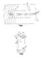
- FIG. 1is a schematic environmental view of several radar applications embodying an electronically scanned lens array (ESA) antenna with microelectromechanical system (MEMS) phase shifters in accordance with the present invention.
- ESAelectronically scanned lens array
- MEMSmicroelectromechanical system
- FIG. 2illustrates a top plan view of a pair of wide band radiating elements and a MEMS phase shifter module in accordance with the present invention.
- FIG. 3illustrates an electronically scanned lens array antenna in accordance with the present invention, the lens antenna including a wide band feedthrough lens with seven MEMS phase shifter modules and a continuous transverse stub (CTS) feed array having seven CTS radiating elements.
- CTScontinuous transverse stub
- FIG. 4is a top plan view of the FIG. 3 electronically scanned lens array antenna, except that the FIG. 4 lens antenna has 16 MEMS phase shifter modules and CTS radiating elements.
- FIG. 5is a cross-sectional view of a segment of the continuous transverse stub (CTS) array of FIG. 3 .
- FIG. 6illustrates a printed circuit board (PCB) including an array of printed wide band radiating elements, and an array of MEMS phase shifter modules on the PCB in accordance with the present invention.
- PCBprinted circuit board
- FIG. 7is a side elevational view of the FIG. 6 PCB and MEMS phase shifter modules as viewed from the line 7 — 7 in FIG. 6 .
- FIG. 8is a bottom view of the FIG. 6 PCB and MEMS phase shifter modules.
- FIG. 9is an enlarged view of a MEMS phase shifter module in accordance with the present invention.
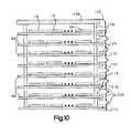
- FIG. 10illustrates a MEMS steerable electronically scanned lens array antenna in accordance with the present invention, showing the mounting structure and connecting lines thereof in greater detail.
- the present inventionis a two dimensional microelectromechanical system (MEMS) steerable electronically scanned lens array antenna 10 (FIG. 3) including a wide band feedthrough lens 11 and a continuous transverse stub (CTS) feed array 12 .
- the wide band feedthrough lens 11includes a rear array of wide band radiating elements 14 a , a front array of wide band radiating elements 14 b , and an array of MEMS phase shifter modules 18 (FIG. 2) sandwiched between the rear and front arrays of radiating elements 14 a and 14 b .
- the CTS feed array 12which is positioned adjacent the rear array of radiating elements 14 a , provides a planar wave front in the near field.
- the MEMS phase shifter modules 18steer a beam radiated from the CTS feed array 12 in two dimensions, that is in the E-plane and H-plane, and, accordingly, the CTS feed array 12 need only generate a fixed beam.
- the present inventionobviates the need for transmission lines, power dividers, and interconnects that are customarily associated with corporate fed antennas.
- the antenna 10is suitable in both commercial and military applications, including for example, aerostats, ships, surveillance aircraft, and spacecraft.
- FIG. 1shows an environmental view of several advanced airborne and space based radar systems in which the antenna 10 may be suitably incorporated. These systems include, for example, lightweight X-band space-based radar for synthetic aperture radar (SAR) systems 22 , ground moving target indication (GMTI) systems 26 , and airborne moving target indication (AMTI) systems 28 .
- SARsynthetic aperture radar
- GMTIground moving target indication
- AMTIairborne moving target indication
- each MEMS phase shifter module 18is sandwiched between a pair of opposite facing wide band radiating elements 14 .
- the radiating elements 14have substantially the same geometry and are disposed symmetrically about the MEMS phase shifter module 18 and about an axis A representing the feed/radiating direction through the antenna 10 and more particularly through the MEMS phase shifter module 18 thereof.
- the radiating elements 14may have a different geometry and/or be disposed asymmetrically about the MEMS phase shifter module 18 and/or the feed/radiating axis A.
- the front or output radiating element 14 bmay have a different geometry than the rear or input radiating element 14 a.
- Each wide band radiating element 14includes a pair of claw-like projections 32 having a rectangular base portion 34 , a relatively narrower stem portion 38 , and an arcuate distal portion 42 .
- the claw-like projections 32form slots 36 therebetween that provide a path along which RF energy propagates (for example, in the direction of the feed/radiating axis A) during operation of the antenna 10 .
- the base portions 34also referred to herein as ground planes, are adjacent one another about the feed/radiating axis A and adjacent the phase shifter module 18 at opposite ends of the phase shifter module 18 in the direction of the feed/radiating axis A. Together the base portions 34 have a 15 width substantially the same as the width of the MEMS phase shifter module 18 .
- the stem portions 38are narrower than the respective base portions 34 and project from the base portions 34 in the direction of the feed/radiating axis A and are also adjacent one another about the feed/radiating axis A.
- the arcuate distal portions 42project from the respective stem portions 38 in the direction of the feed/radiating axis A and branch laterally away from the feed/radiating axis A and away from one another.
- the arcuate distal portions 42together form a flared or arcuate V-shaped opening that flares outward from the phase shifter module 18 in the direction of the feed/radiating axis A.
- the flared opening of a wide band radiating element 14 at the rear end of the wide band feedthrough lens 11receives and channels radio frequency (RF) energy from the CTS feed array 12 , and propagates the RF energy along the corresponding slot 36 to the corresponding MEMS phase shifter module 18 .
- the flared opening of a wide band radiating element 14 at the opposite or front end of the wide band feedthrough lens 11radiates RF energy from the corresponding MEMS phase shifter module 18 along the corresponding slot 36 and into free space.
- the MEMS phase shifters 18are configured as an array in the wide band feedthrough lens 11 .
- the wide band feedthrough lens 11includes an input aperture 54 comprising an array of input radiating elements 14 a behind the MEMS phase shifters 18 , and an output or radiating aperture 58 comprising an array of output radiating elements 14 b in front of the MEMS phase shifters 18 .
- the feedthrough lens 11 of FIG. 3has an array of four (4) rows and seven (7) columns of MEMS phase shifters 18 and four (4) rows and seven (7) columns of input and output radiating elements 14 a and 14 b .
- the arraymay comprise any suitable quantity of MEMS phase shifters 18 and input and output radiating elements 14 a and 14 b as may be desirable for a particular application.
- the wide band feedthrough lens 11includes 16 MEMS phase shifters 18 and 16 input and output wide band radiating elements 14 a and 14 b.
- the wide band feedthrough lens 11is space fed by the CTS feed array 12 .
- the CTS feed array 12illustrated in FIGS. 3 and 4, includes a plurality of RF inputs 62 (four in the FIG. 3 embodiment), a continuous stub 64 and a plurality of CTS radiating elements 68 projecting from the continuous stub 64 toward the input aperture 54 of the wide band feedthrough lens 11 .
- the CTS radiating elements 68correspond in quantity to the input and output radiating elements 14 a and 14 b .
- the CTS radiating elements 68are transversely spaced apart substantially the same distance as the transverse spacing between the input radiating elements 14 a and the transverse spacing between the output radiating elements 14 b .
- the spacing between the CTS radiating elements 68need not be the same as or correspond to the spacing between the input radiating elements 14 a .
- the CTS radiating elements 68 (that is, the columns) and/or the RF inputs 62 (that is, the rows) of the CTS feed array 12need not be the same and/or align with or correspond to the columns and rows of input and output radiating elements 14 a and 14 b and/or the MEMS phase shifter modules 18 of the wide band feedthrough lens 11 .
- the CTS feed array 12may have more or fewer rows and or/columns than the wide band feedthrough lens 11 depending on, for example, the particular antenna application.
- FIG. 5is a cross-sectional view of a segment of the CTS feed array 12 of FIG. 3 .
- the CTS feed array 12includes a dielectric 70 that is made of plastic such as rexolite or polypropylene, and is machined or extruded to the shape shown in FIG. 5 .
- the dielectric 70is then metallized with a metal layer 74 to form the continuous stub 64 and CTS radiating elements 68 .
- the CTS feed array 12lends itself to high volume plastic extrusion and metal plating processes that are common in automotive manufacturing operations and, accordingly, facilitates low production costs.
- the CTS feed array 12is a microwave coupling/radiating array. As is shown in FIG. 5, incident parallel waveguide modes launched via a primary line feed of arbitrary configuration have associated with them longitudinal electric current components interrupted by the presence of the continuous stub 64 , thereby exciting a longitudinal, z-directed displacement current across the stub/parallel plate interface. This induced displacement current in turn excites equivalent electromagnetic waves traveling in the continuous stub 64 in the x direction to the CTS radiating elements 68 into free space. It has been found that such CTS nonscanning antennas may operate at frequencies as high as 94 GHz. For further details relating to an exemplary CTS feed array reference may be had to U.S. Pat. Nos. 6,421,021; 5,361,076; 5,349,363; and 5,266,961, all of which are hereby incorporated herein by reference in their entireties.
- RF energyis series fed from the RF input 62 into the CTS radiating elements 68 via the parallel plate waveguide of the CTS feed array 12 and is radiated out in the form of a plane wave in the near field. It is noted that the distances that the RF energy travels from the RF input 62 to the CTS radiating elements 68 are not equal.
- the RF plane waveis emitted into the input aperture 54 of the wide band feedthrough lens 11 by the CTS radiating elements 68 and then converted into discreet RF signals.
- the RF signalsare then processed by the MEMS phase shifter modules 18 .
- MEMS phase shifter modules 18For further details relating to an MEMS phase shifter reference may be had to U.S. Pat. Nos. 6,281,838; 5,757,379; and 5,379,007, all of which are hereby incorporated herein by reference in their entireties.
- the MEMS processed signalsare then re-radiated out through the radiating aperture 58 of the wide band feedthrough lens 11 , which then recombines the RF signals and forms the steering antenna beam.
- the antenna beammoves at different angular positions along the E-plane 78 (FIG. 3) as a function of frequency, as is illustrated for example at reference numeral 80 in FIG. 4 .
- the output phase of each CTS radiating element 68changes at different rates resulting in frequency scanning.
- a wide band frequencyis achieved by feeding the CTS radiating elements 68 in parallel using a corporate parallel plate waveguide feed (not shown).
- a corporate parallel plate waveguide feed(not shown).
- the distances that the RF energy travels from the RF input 62 to the CTS radiating elements 68are equal.
- the output phase of each CTS radiating element 68changes at substantially the same rate, and thus the antenna beam radiated out through the radiating aperture 58 remains in a fixed position.
- FIGS. 6-10show an exemplary embodiment of an array of wide band radiating elements 14 a and 14 b and MEMS phase shifter modules 18 in which the wide band radiating elements 14 a and 14 b are fabricated onto a printed circuit board (PCB) 84 , and the MEMS phase shifter modules 18 are mounted to the PCB 84 between the input and output radiating elements 14 a and 14 b .
- Each MEMS phase shifter module 18includes a housing 86 (FIG. 9) made of kovar, for example, and a suitable number of MEMS phase shifter switches (not shown), for example two, mounted to the housing 86 . It will be appreciated that the number of MEMS phase shifter switches will depend on the particular application.
- the RF pins 88correspond to the respective input and output radiating elements 14 a and 14 b .
- the RF pins 88extend through the thickness of the PCB 84 in a direction normal to the plane of the PCB 84 , and are electrically connected to respective microstrip transmission lines 104 (that is, a balun) that are mounted on the side of the PCB 84 opposite to that which the RF MEMS phase shifter modules 18 are mounted (FIGS. 7 and 8 ).
- the transmission lines 104are electrically coupled to the respective input and output radiating elements 14 a and 14 b to carry RF signals to and from the input and output radiating elements 14 a and 14 b .
- the transmission lines 104are L-shaped, and have one leg extending across the respective slots 36 in the rectangular base portion 34 (FIG. 2) of the respective radiating elements 14 a and 14 b .
- the rectangular base portion 34functions as a ground plane for the transmission line 104 .
- At the slot 36there is a break across the ground plane (that is, the rectangular portion 34 ) which causes a voltage potential, thereby to force RF energy to propagate along the slot 36 of the respective radiating elements 14 a and 14 b.
- the DC pins 92also extend through the thickness of the PCB 84 and arc electrically connected to DC control signal and bias lines 108 .
- the DC control signal and bias lines 108are routed along the center of the PCB 84 and extend to an edge 110 of the PCB 84 .
- the orientation of the RF pins 88 and the DC pins 92 relative to the plane of the housing 86 of the MEMS phase shifter modules 18enables the RF pins 88 and DC pins 92 to be installed vertically.
- Such vertical interconnect featuremakes installation of the MEMS phase shifter modules 18 relatively simple compared to, for example, conventional MMICS with coaxial connectors or external wire bonds, or other conventional packages having end-to-end type connections requiring numerous process operations.
- the vertical interconnectsprovide flexibility in installation, enabling, for example, a surface mount, pin grid array, or BGA type of package.
- multiple PCBs 84each representing a row of the wide band feedthrough lens 11 may be stacked or vertically arranged in column-like fashion, and spaced apart by spacers 114 .
- the input and output radiating elements 14 a and 14 b of the respective input and radiating apertures 54 and 58 of the wide band feedthrough lens 11are configured in two dimensions, that is a lattice structure of rows and columns of input and output radiating elements 14 a and 14 b is formed.
- the lattice spacingmay be selected based on, for example, the frequency and scanning capabilities desired for a particular application.
- each PCB 84engages a connector 124 .
- the connectors 124are electrically coupled together via a connecting cable 132 , which in turn is connected to a DC distribution printed wiring board (PWB) 138 .
- PWBDC distribution printed wiring board
- an application specific integrated circuit (ASIC) control driver circuit 144which provides the E-plane and H-plane two dimensional scanning, is mounted in or to the housing 86 of each phase shifter module 18 .
- the ASIC circuit 144enables the DC inputs/outputs of adjacent MEMS phase shifter modules 18 to be connected together serially.
- the ASIC circuit 144controls the individual MEMS phase shifter phase settings of the MEMS phase shifter module 18 in which it is installed, and allows serial command and biasing of the MEMS phase shifter switches.
- the design of the ASIC circuit 144may be according to current CMOS IC manufacturing processes, for example.
- the MEMS phase shifter modules 80 and the wide band radiating elements 14 a and 14 b that make up the input aperture 54 and radiating aperture 58 of the wide band feedthrough lens 11as oriented in the illustrated exemplary embodiment, effect E-plane 78 scanning that occurs parallel to the rows of radiating elements 14 a and 14 b , and H-plane scanning that occurs perpendicular to the rows of radiating elements 14 a and 14 b .
- a serial command from a beam steering computeris sent via the DC distribution PWB 138 to each MEMS phase shifter module 18 along the row, where it is received by a differential line receiver built within the ASIC circuit 144 .
- each ASIC circuit 144may be used adjust the bias of each MEMS phase shifter switch to realize a desired phase shift output.
- Each ASIC circuit 144thus effects E-plane and H-plane steering, or two dimensional scanning, of the beam radiated from the antenna 10 .
Landscapes
- Variable-Direction Aerials And Aerial Arrays (AREA)
- Aerials With Secondary Devices (AREA)
- Analysing Materials By The Use Of Radiation (AREA)
- Radar Systems Or Details Thereof (AREA)
- Apparatus For Radiation Diagnosis (AREA)
Abstract
Description
The present invention relates generally to electronically scanned antennas and, more particularly, to an electronic scanned antenna with a microelectromechanical system (MEMS) radio frequency (RF) phase shifter.
Advanced airborne and space based radar systems heretofore have used electronically scanned antennas (ESA) including thousands of radiating elements. For example, large fire control radars that engage multiple targets simultaneously may use ESAs to provide the required power aperture product.
Space based lens architecture is one approach to realizing ESA for airborne and space based radar systems. However, when the space based lens architecture is utilized at higher frequencies, for example, the X-band, and more active components such as phase shifters are packaged within a given area, weight, increased thermal density, and power consumption may deleteriously affect the cost and applicability of such systems.
Heretofore, phase shifter circuits for electronically scanned lens array antennas have included ferrites, PIN diodes and FET switch devices. These phase shifters are heavy, consume a considerable amount of DC power, and are expensive. Also, the implementation of PIN diodes and FET switches into RF phase shifter circuitry is complicated by the need of an additional DC biasing circuit along the RF path. The DC biasing circuit needed by PIN diodes and FET switches limits the phase shifter frequency performance and increases RF losses. Populating the ESA with presently available transmit/receive (TIR) modules is undesirable due to high costs, poor heat dissipation and inefficient power consumption. In sum, the weight, cost and performance of available phase shifter circuits fall short of what is needed for space based radar and communication ESA's, where thousands of these devices are used.
The present invention provides a microelectromechanical system (MEMS) steerable electronically scanned lens array (ESA) antenna. According to an aspect of the invention, the MEMS ESA antenna includes a wide band feedthrough lens and a continuous transverse stub (CTS) feed array. The wide band feedthrough lens includes first and second arrays of wide band radiating elements and an array of MEMS phase shifter modules disposed between the first and second arrays of radiating elements. The continuous transverse stub (CTS) feed array is disposed adjacent the first array of radiating elements for providing a planar wave front in the near field. The MEMS phase shifter modules steer a beam radiated from the CTS feed array in two dimensions.
According to another aspect of the invention, there is provided a method of frequency scanning radio frequency energy, comprising the steps of inputting radio frequency (RIF) energy into a continuous transverse stub (CTS) feed array, radiating the RF energy through a plurality of CTS radiating elements in the form of a plane wave in the near field, emitting the RF plane wave into an input aperture of a wide band feedthrough lens including a plurality of MEMS phase shifter modules, converting the RF wave plane into discreet RF signals, using the MEMS phase shifter modules to process the RF signals, radiating the RF signals through a radiating aperture of the wide band feedthrough lens, thereby recombining the RF signals and forming an antenna beam, and varying the frequency of the RF signal inputted into the CTS feed array thereby to change the angular position of the antenna beam in the E-plane of the wide band feedthrough lens and to effect frequency scanning by the antenna beam.
To the accomplishment of the foregoing and related ends, the invention, then, comprises the features hereinafter fully described and particularly pointed out in the claims. The following description and the annexed drawings set forth in detail certain illustrative embodiments of the invention. These embodiments are indicative, however, of but a few of the various ways in which the principles of the invention may be employed. Other objects, advantages and novel features of the invention will become apparent from the following detailed description of the invention when considered in conjunction with the drawings.
FIG. 1 is a schematic environmental view of several radar applications embodying an electronically scanned lens array (ESA) antenna with microelectromechanical system (MEMS) phase shifters in accordance with the present invention.
FIG. 2 illustrates a top plan view of a pair of wide band radiating elements and a MEMS phase shifter module in accordance with the present invention.
FIG. 3 illustrates an electronically scanned lens array antenna in accordance with the present invention, the lens antenna including a wide band feedthrough lens with seven MEMS phase shifter modules and a continuous transverse stub (CTS) feed array having seven CTS radiating elements.
FIG. 4 is a top plan view of the FIG. 3 electronically scanned lens array antenna, except that the FIG. 4 lens antenna has 16 MEMS phase shifter modules and CTS radiating elements.
FIG. 5 is a cross-sectional view of a segment of the continuous transverse stub (CTS) array of FIG.3.
FIG. 6 illustrates a printed circuit board (PCB) including an array of printed wide band radiating elements, and an array of MEMS phase shifter modules on the PCB in accordance with the present invention.
FIG. 7 is a side elevational view of the FIG. 6 PCB and MEMS phase shifter modules as viewed from theline 7—7 in FIG.6.
FIG. 8 is a bottom view of the FIG. 6 PCB and MEMS phase shifter modules.
FIG. 9 is an enlarged view of a MEMS phase shifter module in accordance with the present invention.
FIG. 10 illustrates a MEMS steerable electronically scanned lens array antenna in accordance with the present invention, showing the mounting structure and connecting lines thereof in greater detail.
In the detailed description that follows, identical components have been given the same reference numerals, regardless of whether they are shown in different embodiments of the present invention. To illustrate the present invention in a clear and concise manner, the drawings may not necessarily be to scale and certain features may be shown in somewhat schematic form.
Referring initially to FIGS. 1-3, the present invention is a two dimensional microelectromechanical system (MEMS) steerable electronically scanned lens array antenna10 (FIG. 3) including a wideband feedthrough lens 11 and a continuous transverse stub (CTS)feed array 12. The wideband feedthrough lens 11 includes a rear array of wideband radiating elements 14a, a front array of wideband radiating elements 14b, and an array of MEMS phase shifter modules18 (FIG. 2) sandwiched between the rear and front arrays ofradiating elements CTS feed array 12, which is positioned adjacent the rear array ofradiating elements 14a, provides a planar wave front in the near field. The MEMSphase shifter modules 18 steer a beam radiated from theCTS feed array 12 in two dimensions, that is in the E-plane and H-plane, and, accordingly, theCTS feed array 12 need only generate a fixed beam. As will be appreciated, the present invention obviates the need for transmission lines, power dividers, and interconnects that are customarily associated with corporate fed antennas.
Theantenna 10 is suitable in both commercial and military applications, including for example, aerostats, ships, surveillance aircraft, and spacecraft. FIG. 1 shows an environmental view of several advanced airborne and space based radar systems in which theantenna 10 may be suitably incorporated. These systems include, for example, lightweight X-band space-based radar for synthetic aperture radar (SAR)systems 22, ground moving target indication (GMTI)systems 26, and airborne moving target indication (AMTI)systems 28. These systems use a substantial number of antennas, and theantenna 10 of the present invention by means of the MEMSphase shifter modules 18 has been found to have a relatively lower cost, use relatively less power, and be lighter in weight than prior art antennas using PIN diode and FET switch phase shifters or transmit/receive (T/R) modules.
As is shown in FIG. 2, each MEMSphase shifter module 18 is sandwiched between a pair of opposite facing wideband radiating elements 14. In the illustrated embodiment, theradiating elements 14 have substantially the same geometry and are disposed symmetrically about the MEMSphase shifter module 18 and about an axis A representing the feed/radiating direction through theantenna 10 and more particularly through the MEMSphase shifter module 18 thereof. As will be appreciated, alternatively theradiating elements 14 may have a different geometry and/or be disposed asymmetrically about the MEMSphase shifter module 18 and/or the feed/radiating axis A. In other words, the front oroutput radiating element 14bmay have a different geometry than the rear orinput radiating element 14a.
Each wideband radiating element 14 includes a pair of claw-like projections 32 having arectangular base portion 34, a relativelynarrower stem portion 38, and an arcuatedistal portion 42. The claw-like projections 32form slots 36 therebetween that provide a path along which RF energy propagates (for example, in the direction of the feed/radiating axis A) during operation of theantenna 10. Thebase portions 34, also referred to herein as ground planes, are adjacent one another about the feed/radiating axis A and adjacent thephase shifter module 18 at opposite ends of thephase shifter module 18 in the direction of the feed/radiating axis A. Together thebase portions 34 have a15 width substantially the same as the width of the MEMSphase shifter module 18. Thestem portions 38 are narrower than therespective base portions 34 and project from thebase portions 34 in the direction of the feed/radiating axis A and are also adjacent one another about the feed/radiating axis A. The arcuatedistal portions 42 project from therespective stem portions 38 in the direction of the feed/radiating axis A and branch laterally away from the feed/radiating axis A and away from one another. The arcuatedistal portions 42 together form a flared or arcuate V-shaped opening that flares outward from thephase shifter module 18 in the direction of the feed/radiating axis A. The flared opening of a wideband radiating element 14 at the rear end of the wideband feedthrough lens 11 receives and channels radio frequency (RF) energy from theCTS feed array 12, and propagates the RF energy along thecorresponding slot 36 to the corresponding MEMSphase shifter module 18. The flared opening of a wideband radiating element 14 at the opposite or front end of the wideband feedthrough lens 11 radiates RF energy from the corresponding MEMSphase shifter module 18 along thecorresponding slot 36 and into free space.
Turning to FIG. 3, theMEMS phase shifters 18 are configured as an array in the wideband feedthrough lens 11. Thus, the wideband feedthrough lens 11 includes aninput aperture 54 comprising an array ofinput radiating elements 14abehind theMEMS phase shifters 18, and an output orradiating aperture 58 comprising an array ofoutput radiating elements 14bin front of theMEMS phase shifters 18. Thefeedthrough lens 11 of FIG. 3 has an array of four (4) rows and seven (7) columns ofMEMS phase shifters 18 and four (4) rows and seven (7) columns of input andoutput radiating elements MEMS phase shifters 18 and input andoutput radiating elements band feedthrough lens 11 includes 16MEMS phase shifters 18 and16 input and output wideband radiating elements
The wideband feedthrough lens 11 is space fed by theCTS feed array 12. TheCTS feed array 12, illustrated in FIGS. 3 and 4, includes a plurality of RF inputs62 (four in the FIG. 3 embodiment), acontinuous stub 64 and a plurality ofCTS radiating elements 68 projecting from thecontinuous stub 64 toward theinput aperture 54 of the wideband feedthrough lens 11. In the illustrated embodiment, theCTS radiating elements 68 correspond in quantity to the input andoutput radiating elements CTS radiating elements 68 are transversely spaced apart substantially the same distance as the transverse spacing between theinput radiating elements 14aand the transverse spacing between theoutput radiating elements 14b. It will be appreciated that the spacing between theCTS radiating elements 68 need not be the same as or correspond to the spacing between theinput radiating elements 14a. Moreover, it will be appreciated that the CTS radiating elements68 (that is, the columns) and/or the RF inputs62 (that is, the rows) of theCTS feed array 12 need not be the same and/or align with or correspond to the columns and rows of input andoutput radiating elements phase shifter modules 18 of the wideband feedthrough lens 11. Thus, theCTS feed array 12 may have more or fewer rows and or/columns than the wideband feedthrough lens 11 depending on, for example, the particular antenna application.
FIG. 5 is a cross-sectional view of a segment of theCTS feed array 12 of FIG.3. TheCTS feed array 12 includes a dielectric70 that is made of plastic such as rexolite or polypropylene, and is machined or extruded to the shape shown in FIG.5. The dielectric70 is then metallized with ametal layer 74 to form thecontinuous stub 64 andCTS radiating elements 68. TheCTS feed array 12 lends itself to high volume plastic extrusion and metal plating processes that are common in automotive manufacturing operations and, accordingly, facilitates low production costs.
TheCTS feed array 12 is a microwave coupling/radiating array. As is shown in FIG. 5, incident parallel waveguide modes launched via a primary line feed of arbitrary configuration have associated with them longitudinal electric current components interrupted by the presence of thecontinuous stub 64, thereby exciting a longitudinal, z-directed displacement current across the stub/parallel plate interface. This induced displacement current in turn excites equivalent electromagnetic waves traveling in thecontinuous stub 64 in the x direction to theCTS radiating elements 68 into free space. It has been found that such CTS nonscanning antennas may operate at frequencies as high as 94 GHz. For further details relating to an exemplary CTS feed array reference may be had to U.S. Pat. Nos. 6,421,021; 5,361,076; 5,349,363; and 5,266,961, all of which are hereby incorporated herein by reference in their entireties.
In operation, RF energy is series fed from theRF input 62 into theCTS radiating elements 68 via the parallel plate waveguide of theCTS feed array 12 and is radiated out in the form of a plane wave in the near field. It is noted that the distances that the RF energy travels from theRF input 62 to theCTS radiating elements 68 are not equal. The RF plane wave is emitted into theinput aperture 54 of the wideband feedthrough lens 11 by theCTS radiating elements 68 and then converted into discreet RF signals. The RF signals are then processed by the MEMSphase shifter modules 18. For further details relating to an MEMS phase shifter reference may be had to U.S. Pat. Nos. 6,281,838; 5,757,379; and 5,379,007, all of which are hereby incorporated herein by reference in their entireties.
The MEMS processed signals are then re-radiated out through the radiatingaperture 58 of the wideband feedthrough lens 11, which then recombines the RF signals and forms the steering antenna beam. For such a series fedCTS feed array 12, the antenna beam moves at different angular positions along the E-plane78 (FIG. 3) as a function of frequency, as is illustrated for example atreference numeral 80 in FIG.4. As the frequency varies, the output phase of eachCTS radiating element 68 changes at different rates resulting in frequency scanning.
In an alternative embodiment, a wide band frequency is achieved by feeding theCTS radiating elements 68 in parallel using a corporate parallel plate waveguide feed (not shown). By parallel feeding theCTS radiating elements 68, the distances that the RF energy travels from theRF input 62 to theCTS radiating elements 68 are equal. As the frequency varies, the output phase of eachCTS radiating element 68 changes at substantially the same rate, and thus the antenna beam radiated out through the radiatingaperture 58 remains in a fixed position.
FIGS. 6-10 show an exemplary embodiment of an array of wideband radiating elements phase shifter modules 18 in which the wideband radiating elements phase shifter modules 18 are mounted to thePCB 84 between the input andoutput radiating elements phase shifter module 18 includes a housing86 (FIG. 9) made of kovar, for example, and a suitable number of MEMS phase shifter switches (not shown), for example two, mounted to thehousing 86. It will be appreciated that the number of MEMS phase shifter switches will depend on the particular application.
A pair of RF pins88 and a plurality of DC pins92 protrude from the bottom of thehousing 86 in a direction substantially normal to the plane of the housing86 (FIG.7). The RF pins88 correspond to the respective input andoutput radiating elements PCB 84 in a direction normal to the plane of thePCB 84, and are electrically connected to respective microstrip transmission lines104 (that is, a balun) that are mounted on the side of thePCB 84 opposite to that which the RF MEMSphase shifter modules 18 are mounted (FIGS.7 and8). Thetransmission lines 104 are electrically coupled to the respective input andoutput radiating elements output radiating elements transmission lines 104 are L-shaped, and have one leg extending across therespective slots 36 in the rectangular base portion34 (FIG. 2) of therespective radiating elements rectangular base portion 34 functions as a ground plane for thetransmission line 104. At theslot 36, there is a break across the ground plane (that is, the rectangular portion34) which causes a voltage potential, thereby to force RF energy to propagate along theslot 36 of therespective radiating elements
The DC pins92 also extend through the thickness of thePCB 84 and arc electrically connected to DC control signal and bias lines108. The DC control signal andbias lines 108 are routed along the center of thePCB 84 and extend to anedge 110 of thePCB 84.
It will be appreciated that the orientation of the RF pins88 and the DC pins92 relative to the plane of thehousing 86 of the MEMSphase shifter modules 18 enables the RF pins88 and DC pins92 to be installed vertically. Such vertical interconnect feature makes installation of the MEMSphase shifter modules 18 relatively simple compared to, for example, conventional MMICS with coaxial connectors or external wire bonds, or other conventional packages having end-to-end type connections requiring numerous process operations. The vertical interconnects provide flexibility in installation, enabling, for example, a surface mount, pin grid array, or BGA type of package.
As is shown in FIG. 10, multiple PCBs84 (eight in the illustrated exemplary embodiment) each representing a row of the wideband feedthrough lens 11 may be stacked or vertically arranged in column-like fashion, and spaced apart byspacers 114. In this way, the input andoutput radiating elements apertures band feedthrough lens 11 are configured in two dimensions, that is a lattice structure of rows and columns of input andoutput radiating elements
The DC control signal andbias lines 108 of eachPCB 84 engage aconnector 124. In the illustrated embodiment, there are eightconnectors 124. Theconnectors 124 in turn are electrically coupled together via a connectingcable 132, which in turn is connected to a DC distribution printed wiring board (PWB)138.
Referring again to FIG. 9, an application specific integrated circuit (ASIC)control driver circuit 144, which provides the E-plane and H-plane two dimensional scanning, is mounted in or to thehousing 86 of eachphase shifter module 18. TheASIC circuit 144 enables the DC inputs/outputs of adjacent MEMSphase shifter modules 18 to be connected together serially. TheASIC circuit 144 controls the individual MEMS phase shifter phase settings of the MEMSphase shifter module 18 in which it is installed, and allows serial command and biasing of the MEMS phase shifter switches. As will be appreciated, the design of theASIC circuit 144 may be according to current CMOS IC manufacturing processes, for example.
Together, the MEMSphase shifter modules 80 and the wideband radiating elements input aperture 54 and radiatingaperture 58 of the wideband feedthrough lens 11, as oriented in the illustrated exemplary embodiment, effect E-plane78 scanning that occurs parallel to the rows of radiatingelements elements phase shifter module 18, a serial command from a beam steering computer is sent via theDC distribution PWB 138 to each MEMSphase shifter module 18 along the row, where it is received by a differential line receiver built within theASIC circuit 144. The logic control circuitry built within eachASIC circuit 144 may be used adjust the bias of each MEMS phase shifter switch to realize a desired phase shift output. EachASIC circuit 144 thus effects E-plane and H-plane steering, or two dimensional scanning, of the beam radiated from theantenna 10.
Although the invention has been shown and described with respect to certain illustrated embodiments, equivalent alterations and modifications will occur to others skilled in the art upon reading and understanding this specification and the annexed drawings. In particular regard to the various functions performed by the above described integers (components, assemblies, devices, compositions, etc.), the terms (including a reference to a “means”) used to describe such integers are intended to correspond, unless otherwise indicated, to any integer which performs the specified function of the described integer (i.e., that is functionally equivalent), even though not structurally equivalent to the disclosed structure which performs the function in the herein illustrated exemplary embodiment or embodiments of the invention. In addition, while a particular feature of the invention may have been described above with respect to only one of several illustrated embodiments, such feature may be combined with one or more other features of the other embodiments, as may be desired and advantageous for any given or particular application.
The present invention includes all such equivalents and modifications, and is scope of the following claims.
Claims (14)
1. A microelectromechanical system (MEMS) steerable electronically scanned lens array (ESA) antenna, comprising:
a wide band feedthrough lens including first and second arrays of wide band radiating elements, and an array of MEMS phase shifter modules disposed between the first and second arrays of radiating elements; and,
a continuous transverse stub (CTS) feed array disposed adjacent the first array of radiating elements for providing a planar wave front in the near field;
wherein the MEMS phase shifter modules steer a beam radiated from the CTS feed array in two dimensions.
2. The MEMS ESA antenna ofclaim 1 , wherein the first and second arrays of wide band radiating elements are fabricated onto a printed circuit board (PCB), and the MEMS phase shifter modules are mounted to the PCB between the input and output wide band radiating elements.
3. The MEMS ESA antenna ofclaim 2 , wherein each MEMS phase shifter module includes a pair of RF pins corresponding to respective first and second radiating elements of the first and second arrays of radiating elements of the wide band feed through lens.
4. The MEMS ESA antenna ofclaim 3 , wherein the RF pins extend through the thickness of the PCB and electrically connect to respective microstrip transmission lines that are mounted on the side of the PCB opposite to that which the RF MEMS phase shifter modules are mounted, the microstrip transmission lines being operative to carry the RF signals to and from the respective first and second radiating elements.
5. The MEMS ESA antenna ofclaim 2 , wherein each MEMS phase shifter module includes a plurality of DC pins that extend through the thickness of the PCB and electrically connect to respective DC control signal and bias lines that are mounted on the side of the PCB opposite to that which the RF MEMS phase shifter module are mounted, and are routed along the center of the PCB and extend to an edge of the PCB, where the DC control signal and bias lines DC are connected to a DC distribution line.
6. The MEMS ESA antenna ofclaim 2 , wherein each MEMS phase shifter module includes a pair of RF pins corresponding to respective first and second radiating elements of the first and second arrays of radiating elements of the wide band feedthrough lens, and a plurality of DC pins for receiving serial commands from a beam steering computer to at least partially steer the beam radiated from the CTS feed array, and wherein the RF pins and DC pins arc oriented perpendicularly with respect to a housing of the respective MEMS phase shifter module to enable interconnection of same to the PCB in a relatively vertical manner.
7. The MEMS ESA antenna ofclaim 2 , wherein two or more PCBs are vertically arranged in column-like fashion and spaced apart by spacers to form a lattice structure of rows and columns of radiating elements.
8. The MEMS ESA antenna ofclaim 7 , wherein the lattice spacing is based on the frequency and scanning capabilities of an antenna application.
9. The MEMS ESA antenna ofclaim 1 , further including an application specific integrated circuit (ASIC) control/driver circuit mounted with respect to each phase shifter module to connect electrically serially together adjacent MEMS phase shifter modules and to control individual phase settings of the respective MEMS phase shifter module.
10. The MEMS ESA antenna ofclaim 1 , wherein the wide band radiating elements of the wide band feedthrough lens are oriented such that E-plane scanning occurs parallel to the rows of radiating elements.
11. A method of frequency scanning radio frequency energy, comprising the steps of.
inputting radio frequency (RF) energy into a continuous transverse stub (CTS) feed array;
radiating the RF energy through a plurality of CTS radiating elements in the form of a plane wave in the near field;
emitting the RF plane wave into an input aperture of a wide band feedthrough lens including a plurality of MEMS phase shifter modules;
converting the RF plane wave into discreet RF signals;
using the MEMS phase shifter modules to process the RF signals;
radiating the RF signals through a radiating aperture of the wide band feedthrough lens, thereby recombining the RF signals and forming an antenna beam; and,
varying the frequency of the RF signal inputted into the CTS feed array thereby to change the angular position of the antenna beam in two dimensions and to effect frequency scanning by the antenna beam.
12. The method ofclaim 11 , wherein the step of inputting RF energy includes feeding the CTS radiating elements in series.
13. The method ofclaim 12 , further including the step of adjusting the phase shifter output for the respective MEMS phase shifter modules by adjusting the bias of one or more MEMS phase shifter switches in the respective MEMS phase shifter module.
14. The method ofclaim 13 , wherein the step of adjusting the bias of one or more MEMS phase shifter switches includes sending a serial command from a beam steering computer to the respective MEMS phase shifter module and using an ASIC circuit to process the command and thereby adjust the bias of the one or more MEMS phase shifter switches.
Priority Applications (10)
| Application Number | Priority Date | Filing Date | Title |
|---|---|---|---|
| US10/373,936US6822615B2 (en) | 2003-02-25 | 2003-02-25 | Wideband 2-D electronically scanned array with compact CTS feed and MEMS phase shifters |
| EP04709527AEP1597793B1 (en) | 2003-02-25 | 2004-02-09 | Wideband 2-d electronically scanned array with compact cts feed and mems phase shifters |
| DE602004015571TDE602004015571D1 (en) | 2003-02-25 | 2004-02-09 | ELECTRONICALLY SCANNING 2-D BROADBAND ARRAY WITH COMPACT CTS SUPPLY AND MEMS PHASE SLIDERS |
| ES04709527TES2310282T3 (en) | 2003-02-25 | 2004-02-09 | 2-D (BIDIMENSIONAL) WIDE-BAND ELECTRONIC SWEEP NETWORK WITH CTS POWER SUPPLY (CONTINUOUS TRANSVERSE ELEMENT) AND MEMS CHANNELS (MICROELECTROMECHANICAL SYSTEM). |
| PCT/US2004/003905WO2004077607A2 (en) | 2003-02-25 | 2004-02-09 | Wideband 2-d electronically scanned array with compact cts feed and mems phase shifters |
| DK04709527TDK1597793T3 (en) | 2003-02-25 | 2004-02-09 | Electronically scanned 2D broadband array with compact CTS power supply and MEMS phase switches |
| KR1020057015721AKR100655823B1 (en) | 2003-02-25 | 2004-02-09 | Wideband 2-d electronically scanned array with compact cts feed and mems phase shifters |
| JP2006503462AJP4563996B2 (en) | 2003-02-25 | 2004-02-09 | Broadband two-dimensional electronic scanning array with compact CTS feed and MEMS phase shifter |
| AT04709527TATE403947T1 (en) | 2003-02-25 | 2004-02-09 | ELECTRONICALLY SCANNING 2-D BROADBAND ARRAY WITH COMPACT CTS POWER AND MEMS PHASE SHIFTERS |
| NO20054415ANO336360B1 (en) | 2003-02-25 | 2005-09-23 | Broadband 2-D electronically scanned group antenna with compact CTS power supply and MEMS phase switches |
Applications Claiming Priority (1)
| Application Number | Priority Date | Filing Date | Title |
|---|---|---|---|
| US10/373,936US6822615B2 (en) | 2003-02-25 | 2003-02-25 | Wideband 2-D electronically scanned array with compact CTS feed and MEMS phase shifters |
Publications (2)
| Publication Number | Publication Date |
|---|---|
| US20040164915A1 US20040164915A1 (en) | 2004-08-26 |
| US6822615B2true US6822615B2 (en) | 2004-11-23 |
Family
ID=32868769
Family Applications (1)
| Application Number | Title | Priority Date | Filing Date |
|---|---|---|---|
| US10/373,936Expired - LifetimeUS6822615B2 (en) | 2003-02-25 | 2003-02-25 | Wideband 2-D electronically scanned array with compact CTS feed and MEMS phase shifters |
Country Status (10)
| Country | Link |
|---|---|
| US (1) | US6822615B2 (en) |
| EP (1) | EP1597793B1 (en) |
| JP (1) | JP4563996B2 (en) |
| KR (1) | KR100655823B1 (en) |
| AT (1) | ATE403947T1 (en) |
| DE (1) | DE602004015571D1 (en) |
| DK (1) | DK1597793T3 (en) |
| ES (1) | ES2310282T3 (en) |
| NO (1) | NO336360B1 (en) |
| WO (1) | WO2004077607A2 (en) |
Cited By (173)
| Publication number | Priority date | Publication date | Assignee | Title |
|---|---|---|---|---|
| US7030824B1 (en)* | 2003-05-29 | 2006-04-18 | Lockheed Martin Corporation | MEMS reflectarray antenna for satellite applications |
| US20060132369A1 (en)* | 2004-12-20 | 2006-06-22 | Robertson Ralston S | Transverse device array radiator ESA |
| US20060267850A1 (en)* | 2005-05-24 | 2006-11-30 | Krikorian Kapriel V | Variable inclination array antenna |
| US20060273973A1 (en)* | 2005-06-02 | 2006-12-07 | Chandler Cole A | Millimeter wave passive electronically scanned antenna |
| US20080007472A1 (en)* | 2006-07-06 | 2008-01-10 | Ibahn General Holdings Corporation | Antenna designs for multi-path environments |
| US20100231452A1 (en)* | 2005-09-23 | 2010-09-16 | California Institute Of Technology | Mm-wave fully integrated phased array receiver and transmitter with on-chip antennas |
| US20110057860A1 (en)* | 2009-09-07 | 2011-03-10 | Kabushiki Kaisha Toshiba | Transmission and reception module |
| US9119127B1 (en) | 2012-12-05 | 2015-08-25 | At&T Intellectual Property I, Lp | Backhaul link for distributed antenna system |
| US9154966B2 (en) | 2013-11-06 | 2015-10-06 | At&T Intellectual Property I, Lp | Surface-wave communications and methods thereof |
| US9209902B2 (en) | 2013-12-10 | 2015-12-08 | At&T Intellectual Property I, L.P. | Quasi-optical coupler |
| US9312919B1 (en) | 2014-10-21 | 2016-04-12 | At&T Intellectual Property I, Lp | Transmission device with impairment compensation and methods for use therewith |
| US9461706B1 (en) | 2015-07-31 | 2016-10-04 | At&T Intellectual Property I, Lp | Method and apparatus for exchanging communication signals |
| US9490869B1 (en) | 2015-05-14 | 2016-11-08 | At&T Intellectual Property I, L.P. | Transmission medium having multiple cores and methods for use therewith |
| US9503189B2 (en) | 2014-10-10 | 2016-11-22 | At&T Intellectual Property I, L.P. | Method and apparatus for arranging communication sessions in a communication system |
| US9509415B1 (en) | 2015-06-25 | 2016-11-29 | At&T Intellectual Property I, L.P. | Methods and apparatus for inducing a fundamental wave mode on a transmission medium |
| US9520945B2 (en) | 2014-10-21 | 2016-12-13 | At&T Intellectual Property I, L.P. | Apparatus for providing communication services and methods thereof |
| US9525524B2 (en) | 2013-05-31 | 2016-12-20 | At&T Intellectual Property I, L.P. | Remote distributed antenna system |
| US9525210B2 (en) | 2014-10-21 | 2016-12-20 | At&T Intellectual Property I, L.P. | Guided-wave transmission device with non-fundamental mode propagation and methods for use therewith |
| US9531427B2 (en) | 2014-11-20 | 2016-12-27 | At&T Intellectual Property I, L.P. | Transmission device with mode division multiplexing and methods for use therewith |
| US9564947B2 (en) | 2014-10-21 | 2017-02-07 | At&T Intellectual Property I, L.P. | Guided-wave transmission device with diversity and methods for use therewith |
| US9577307B2 (en) | 2014-10-21 | 2017-02-21 | At&T Intellectual Property I, L.P. | Guided-wave transmission device and methods for use therewith |
| US20170085003A1 (en)* | 2015-07-14 | 2017-03-23 | At&T Intellectual Property I, L.P. | Apparatus and methods for communicating utilizing an antenna array |
| US9608740B2 (en) | 2015-07-15 | 2017-03-28 | At&T Intellectual Property I, L.P. | Method and apparatus for launching a wave mode that mitigates interference |
| US9608692B2 (en) | 2015-06-11 | 2017-03-28 | At&T Intellectual Property I, L.P. | Repeater and methods for use therewith |
| US20170093693A1 (en)* | 2015-07-14 | 2017-03-30 | At&T Intellectual Property I, L.P. | Apparatus and methods for communicating utilizing an antenna array and multiple communication paths |
| US9615269B2 (en) | 2014-10-02 | 2017-04-04 | At&T Intellectual Property I, L.P. | Method and apparatus that provides fault tolerance in a communication network |
| US9628854B2 (en) | 2014-09-29 | 2017-04-18 | At&T Intellectual Property I, L.P. | Method and apparatus for distributing content in a communication network |
| US9628116B2 (en) | 2015-07-14 | 2017-04-18 | At&T Intellectual Property I, L.P. | Apparatus and methods for transmitting wireless signals |
| US9640850B2 (en) | 2015-06-25 | 2017-05-02 | At&T Intellectual Property I, L.P. | Methods and apparatus for inducing a non-fundamental wave mode on a transmission medium |
| US9654173B2 (en) | 2014-11-20 | 2017-05-16 | At&T Intellectual Property I, L.P. | Apparatus for powering a communication device and methods thereof |
| US9653770B2 (en) | 2014-10-21 | 2017-05-16 | At&T Intellectual Property I, L.P. | Guided wave coupler, coupling module and methods for use therewith |
| US9667317B2 (en) | 2015-06-15 | 2017-05-30 | At&T Intellectual Property I, L.P. | Method and apparatus for providing security using network traffic adjustments |
| US9680670B2 (en) | 2014-11-20 | 2017-06-13 | At&T Intellectual Property I, L.P. | Transmission device with channel equalization and control and methods for use therewith |
| US9685992B2 (en) | 2014-10-03 | 2017-06-20 | At&T Intellectual Property I, L.P. | Circuit panel network and methods thereof |
| US9692101B2 (en) | 2014-08-26 | 2017-06-27 | At&T Intellectual Property I, L.P. | Guided wave couplers for coupling electromagnetic waves between a waveguide surface and a surface of a wire |
| US9705571B2 (en) | 2015-09-16 | 2017-07-11 | At&T Intellectual Property I, L.P. | Method and apparatus for use with a radio distributed antenna system |
| US9705561B2 (en) | 2015-04-24 | 2017-07-11 | At&T Intellectual Property I, L.P. | Directional coupling device and methods for use therewith |
| US9722318B2 (en) | 2015-07-14 | 2017-08-01 | At&T Intellectual Property I, L.P. | Method and apparatus for coupling an antenna to a device |
| US9729197B2 (en) | 2015-10-01 | 2017-08-08 | At&T Intellectual Property I, L.P. | Method and apparatus for communicating network management traffic over a network |
| US9735833B2 (en) | 2015-07-31 | 2017-08-15 | At&T Intellectual Property I, L.P. | Method and apparatus for communications management in a neighborhood network |
| US9742462B2 (en) | 2014-12-04 | 2017-08-22 | At&T Intellectual Property I, L.P. | Transmission medium and communication interfaces and methods for use therewith |
| US9749053B2 (en) | 2015-07-23 | 2017-08-29 | At&T Intellectual Property I, L.P. | Node device, repeater and methods for use therewith |
| US9749013B2 (en) | 2015-03-17 | 2017-08-29 | At&T Intellectual Property I, L.P. | Method and apparatus for reducing attenuation of electromagnetic waves guided by a transmission medium |
| US9748626B2 (en) | 2015-05-14 | 2017-08-29 | At&T Intellectual Property I, L.P. | Plurality of cables having different cross-sectional shapes which are bundled together to form a transmission medium |
| US9755697B2 (en) | 2014-09-15 | 2017-09-05 | At&T Intellectual Property I, L.P. | Method and apparatus for sensing a condition in a transmission medium of electromagnetic waves |
| US9762289B2 (en) | 2014-10-14 | 2017-09-12 | At&T Intellectual Property I, L.P. | Method and apparatus for transmitting or receiving signals in a transportation system |
| US9769020B2 (en) | 2014-10-21 | 2017-09-19 | At&T Intellectual Property I, L.P. | Method and apparatus for responding to events affecting communications in a communication network |
| US9769128B2 (en) | 2015-09-28 | 2017-09-19 | At&T Intellectual Property I, L.P. | Method and apparatus for encryption of communications over a network |
| US9780834B2 (en) | 2014-10-21 | 2017-10-03 | At&T Intellectual Property I, L.P. | Method and apparatus for transmitting electromagnetic waves |
| US9793951B2 (en) | 2015-07-15 | 2017-10-17 | At&T Intellectual Property I, L.P. | Method and apparatus for launching a wave mode that mitigates interference |
| US9793954B2 (en) | 2015-04-28 | 2017-10-17 | At&T Intellectual Property I, L.P. | Magnetic coupling device and methods for use therewith |
| US9793955B2 (en) | 2015-04-24 | 2017-10-17 | At&T Intellectual Property I, Lp | Passive electrical coupling device and methods for use therewith |
| US9800396B1 (en) | 2016-12-16 | 2017-10-24 | Industrial Technology Research Institute | Transmitter and receiver |
| US9800327B2 (en) | 2014-11-20 | 2017-10-24 | At&T Intellectual Property I, L.P. | Apparatus for controlling operations of a communication device and methods thereof |
| US9820146B2 (en) | 2015-06-12 | 2017-11-14 | At&T Intellectual Property I, L.P. | Method and apparatus for authentication and identity management of communicating devices |
| US9838896B1 (en) | 2016-12-09 | 2017-12-05 | At&T Intellectual Property I, L.P. | Method and apparatus for assessing network coverage |
| US9836957B2 (en) | 2015-07-14 | 2017-12-05 | At&T Intellectual Property I, L.P. | Method and apparatus for communicating with premises equipment |
| US9847850B2 (en) | 2014-10-14 | 2017-12-19 | At&T Intellectual Property I, L.P. | Method and apparatus for adjusting a mode of communication in a communication network |
| US9847566B2 (en) | 2015-07-14 | 2017-12-19 | At&T Intellectual Property I, L.P. | Method and apparatus for adjusting a field of a signal to mitigate interference |
| US9853342B2 (en) | 2015-07-14 | 2017-12-26 | At&T Intellectual Property I, L.P. | Dielectric transmission medium connector and methods for use therewith |
| US9860075B1 (en) | 2016-08-26 | 2018-01-02 | At&T Intellectual Property I, L.P. | Method and communication node for broadband distribution |
| US9865911B2 (en) | 2015-06-25 | 2018-01-09 | At&T Intellectual Property I, L.P. | Waveguide system for slot radiating first electromagnetic waves that are combined into a non-fundamental wave mode second electromagnetic wave on a transmission medium |
| US9866309B2 (en) | 2015-06-03 | 2018-01-09 | At&T Intellectual Property I, Lp | Host node device and methods for use therewith |
| DE102016112582A1 (en)* | 2016-07-08 | 2018-01-11 | Lisa Dräxlmaier GmbH | Phased array antenna element |
| DE102016112581A1 (en)* | 2016-07-08 | 2018-01-11 | Lisa Dräxlmaier GmbH | Phased array antenna |
| US9871282B2 (en) | 2015-05-14 | 2018-01-16 | At&T Intellectual Property I, L.P. | At least one transmission medium having a dielectric surface that is covered at least in part by a second dielectric |
| US9871283B2 (en) | 2015-07-23 | 2018-01-16 | At&T Intellectual Property I, Lp | Transmission medium having a dielectric core comprised of plural members connected by a ball and socket configuration |
| US9876570B2 (en) | 2015-02-20 | 2018-01-23 | At&T Intellectual Property I, Lp | Guided-wave transmission device with non-fundamental mode propagation and methods for use therewith |
| US9876605B1 (en) | 2016-10-21 | 2018-01-23 | At&T Intellectual Property I, L.P. | Launcher and coupling system to support desired guided wave mode |
| US9876264B2 (en) | 2015-10-02 | 2018-01-23 | At&T Intellectual Property I, Lp | Communication system, guided wave switch and methods for use therewith |
| US9882257B2 (en) | 2015-07-14 | 2018-01-30 | At&T Intellectual Property I, L.P. | Method and apparatus for launching a wave mode that mitigates interference |
| US9882277B2 (en) | 2015-10-02 | 2018-01-30 | At&T Intellectual Property I, Lp | Communication device and antenna assembly with actuated gimbal mount |
| US9893795B1 (en) | 2016-12-07 | 2018-02-13 | At&T Intellectual Property I, Lp | Method and repeater for broadband distribution |
| US9906269B2 (en) | 2014-09-17 | 2018-02-27 | At&T Intellectual Property I, L.P. | Monitoring and mitigating conditions in a communication network |
| US9904535B2 (en) | 2015-09-14 | 2018-02-27 | At&T Intellectual Property I, L.P. | Method and apparatus for distributing software |
| US9913139B2 (en) | 2015-06-09 | 2018-03-06 | At&T Intellectual Property I, L.P. | Signal fingerprinting for authentication of communicating devices |
| US9912381B2 (en) | 2015-06-03 | 2018-03-06 | At&T Intellectual Property I, Lp | Network termination and methods for use therewith |
| US9911020B1 (en) | 2016-12-08 | 2018-03-06 | At&T Intellectual Property I, L.P. | Method and apparatus for tracking via a radio frequency identification device |
| US9912027B2 (en) | 2015-07-23 | 2018-03-06 | At&T Intellectual Property I, L.P. | Method and apparatus for exchanging communication signals |
| US9912419B1 (en) | 2016-08-24 | 2018-03-06 | At&T Intellectual Property I, L.P. | Method and apparatus for managing a fault in a distributed antenna system |
| US9917341B2 (en) | 2015-05-27 | 2018-03-13 | At&T Intellectual Property I, L.P. | Apparatus and method for launching electromagnetic waves and for modifying radial dimensions of the propagating electromagnetic waves |
| US9927517B1 (en) | 2016-12-06 | 2018-03-27 | At&T Intellectual Property I, L.P. | Apparatus and methods for sensing rainfall |
| US9948333B2 (en) | 2015-07-23 | 2018-04-17 | At&T Intellectual Property I, L.P. | Method and apparatus for wireless communications to mitigate interference |
| US9948354B2 (en) | 2015-04-28 | 2018-04-17 | At&T Intellectual Property I, L.P. | Magnetic coupling device with reflective plate and methods for use therewith |
| US9954287B2 (en) | 2014-11-20 | 2018-04-24 | At&T Intellectual Property I, L.P. | Apparatus for converting wireless signals and electromagnetic waves and methods thereof |
| US9966670B1 (en) | 2016-12-27 | 2018-05-08 | Industrial Technology Research Institute | Transmitting device and receiving device |
| US9967173B2 (en) | 2015-07-31 | 2018-05-08 | At&T Intellectual Property I, L.P. | Method and apparatus for authentication and identity management of communicating devices |
| US9973940B1 (en) | 2017-02-27 | 2018-05-15 | At&T Intellectual Property I, L.P. | Apparatus and methods for dynamic impedance matching of a guided wave launcher |
| US9991580B2 (en) | 2016-10-21 | 2018-06-05 | At&T Intellectual Property I, L.P. | Launcher and coupling system for guided wave mode cancellation |
| US9999038B2 (en) | 2013-05-31 | 2018-06-12 | At&T Intellectual Property I, L.P. | Remote distributed antenna system |
| US9997819B2 (en) | 2015-06-09 | 2018-06-12 | At&T Intellectual Property I, L.P. | Transmission medium and method for facilitating propagation of electromagnetic waves via a core |
| US9998870B1 (en) | 2016-12-08 | 2018-06-12 | At&T Intellectual Property I, L.P. | Method and apparatus for proximity sensing |
| US10009067B2 (en) | 2014-12-04 | 2018-06-26 | At&T Intellectual Property I, L.P. | Method and apparatus for configuring a communication interface |
| US10009065B2 (en) | 2012-12-05 | 2018-06-26 | At&T Intellectual Property I, L.P. | Backhaul link for distributed antenna system |
| US10009063B2 (en) | 2015-09-16 | 2018-06-26 | At&T Intellectual Property I, L.P. | Method and apparatus for use with a radio distributed antenna system having an out-of-band reference signal |
| US10009901B2 (en) | 2015-09-16 | 2018-06-26 | At&T Intellectual Property I, L.P. | Method, apparatus, and computer-readable storage medium for managing utilization of wireless resources between base stations |
| US10020844B2 (en) | 2016-12-06 | 2018-07-10 | T&T Intellectual Property I, L.P. | Method and apparatus for broadcast communication via guided waves |
| US10020587B2 (en) | 2015-07-31 | 2018-07-10 | At&T Intellectual Property I, L.P. | Radial antenna and methods for use therewith |
| US10027397B2 (en) | 2016-12-07 | 2018-07-17 | At&T Intellectual Property I, L.P. | Distributed antenna system and methods for use therewith |
| US10033107B2 (en) | 2015-07-14 | 2018-07-24 | At&T Intellectual Property I, L.P. | Method and apparatus for coupling an antenna to a device |
| US10033108B2 (en) | 2015-07-14 | 2018-07-24 | At&T Intellectual Property I, L.P. | Apparatus and methods for generating an electromagnetic wave having a wave mode that mitigates interference |
| US10044409B2 (en) | 2015-07-14 | 2018-08-07 | At&T Intellectual Property I, L.P. | Transmission medium and methods for use therewith |
| US10051483B2 (en) | 2015-10-16 | 2018-08-14 | At&T Intellectual Property I, L.P. | Method and apparatus for directing wireless signals |
| US10051629B2 (en) | 2015-09-16 | 2018-08-14 | At&T Intellectual Property I, L.P. | Method and apparatus for use with a radio distributed antenna system having an in-band reference signal |
| US10069535B2 (en) | 2016-12-08 | 2018-09-04 | At&T Intellectual Property I, L.P. | Apparatus and methods for launching electromagnetic waves having a certain electric field structure |
| US10074890B2 (en) | 2015-10-02 | 2018-09-11 | At&T Intellectual Property I, L.P. | Communication device and antenna with integrated light assembly |
| US10079661B2 (en) | 2015-09-16 | 2018-09-18 | At&T Intellectual Property I, L.P. | Method and apparatus for use with a radio distributed antenna system having a clock reference |
| US10090606B2 (en) | 2015-07-15 | 2018-10-02 | At&T Intellectual Property I, L.P. | Antenna system with dielectric array and methods for use therewith |
| US10090594B2 (en) | 2016-11-23 | 2018-10-02 | At&T Intellectual Property I, L.P. | Antenna system having structural configurations for assembly |
| US10103801B2 (en) | 2015-06-03 | 2018-10-16 | At&T Intellectual Property I, L.P. | Host node device and methods for use therewith |
| US10103422B2 (en) | 2016-12-08 | 2018-10-16 | At&T Intellectual Property I, L.P. | Method and apparatus for mounting network devices |
| US10135147B2 (en) | 2016-10-18 | 2018-11-20 | At&T Intellectual Property I, L.P. | Apparatus and methods for launching guided waves via an antenna |
| US10136434B2 (en) | 2015-09-16 | 2018-11-20 | At&T Intellectual Property I, L.P. | Method and apparatus for use with a radio distributed antenna system having an ultra-wideband control channel |
| US10135145B2 (en) | 2016-12-06 | 2018-11-20 | At&T Intellectual Property I, L.P. | Apparatus and methods for generating an electromagnetic wave along a transmission medium |
| US10135146B2 (en) | 2016-10-18 | 2018-11-20 | At&T Intellectual Property I, L.P. | Apparatus and methods for launching guided waves via circuits |
| US10142086B2 (en) | 2015-06-11 | 2018-11-27 | At&T Intellectual Property I, L.P. | Repeater and methods for use therewith |
| US10139820B2 (en) | 2016-12-07 | 2018-11-27 | At&T Intellectual Property I, L.P. | Method and apparatus for deploying equipment of a communication system |
| US10144036B2 (en) | 2015-01-30 | 2018-12-04 | At&T Intellectual Property I, L.P. | Method and apparatus for mitigating interference affecting a propagation of electromagnetic waves guided by a transmission medium |
| US10154493B2 (en) | 2015-06-03 | 2018-12-11 | At&T Intellectual Property I, L.P. | Network termination and methods for use therewith |
| US10170840B2 (en) | 2015-07-14 | 2019-01-01 | At&T Intellectual Property I, L.P. | Apparatus and methods for sending or receiving electromagnetic signals |
| US10168695B2 (en) | 2016-12-07 | 2019-01-01 | At&T Intellectual Property I, L.P. | Method and apparatus for controlling an unmanned aircraft |
| US10178445B2 (en) | 2016-11-23 | 2019-01-08 | At&T Intellectual Property I, L.P. | Methods, devices, and systems for load balancing between a plurality of waveguides |
| US10225025B2 (en) | 2016-11-03 | 2019-03-05 | At&T Intellectual Property I, L.P. | Method and apparatus for detecting a fault in a communication system |
| US10224634B2 (en) | 2016-11-03 | 2019-03-05 | At&T Intellectual Property I, L.P. | Methods and apparatus for adjusting an operational characteristic of an antenna |
| US10243270B2 (en) | 2016-12-07 | 2019-03-26 | At&T Intellectual Property I, L.P. | Beam adaptive multi-feed dielectric antenna system and methods for use therewith |
| US10243784B2 (en) | 2014-11-20 | 2019-03-26 | At&T Intellectual Property I, L.P. | System for generating topology information and methods thereof |
| US10264586B2 (en) | 2016-12-09 | 2019-04-16 | At&T Mobility Ii Llc | Cloud-based packet controller and methods for use therewith |
| US10291311B2 (en) | 2016-09-09 | 2019-05-14 | At&T Intellectual Property I, L.P. | Method and apparatus for mitigating a fault in a distributed antenna system |
| US10291334B2 (en) | 2016-11-03 | 2019-05-14 | At&T Intellectual Property I, L.P. | System for detecting a fault in a communication system |
| US10298293B2 (en) | 2017-03-13 | 2019-05-21 | At&T Intellectual Property I, L.P. | Apparatus of communication utilizing wireless network devices |
| US10305190B2 (en) | 2016-12-01 | 2019-05-28 | At&T Intellectual Property I, L.P. | Reflecting dielectric antenna system and methods for use therewith |
| US10312567B2 (en) | 2016-10-26 | 2019-06-04 | At&T Intellectual Property I, L.P. | Launcher with planar strip antenna and methods for use therewith |
| US10320586B2 (en) | 2015-07-14 | 2019-06-11 | At&T Intellectual Property I, L.P. | Apparatus and methods for generating non-interfering electromagnetic waves on an insulated transmission medium |
| US10326494B2 (en) | 2016-12-06 | 2019-06-18 | At&T Intellectual Property I, L.P. | Apparatus for measurement de-embedding and methods for use therewith |
| US10326689B2 (en) | 2016-12-08 | 2019-06-18 | At&T Intellectual Property I, L.P. | Method and system for providing alternative communication paths |
| US10340600B2 (en) | 2016-10-18 | 2019-07-02 | At&T Intellectual Property I, L.P. | Apparatus and methods for launching guided waves via plural waveguide systems |
| US10340573B2 (en) | 2016-10-26 | 2019-07-02 | At&T Intellectual Property I, L.P. | Launcher with cylindrical coupling device and methods for use therewith |
| US10340983B2 (en) | 2016-12-09 | 2019-07-02 | At&T Intellectual Property I, L.P. | Method and apparatus for surveying remote sites via guided wave communications |
| US10340603B2 (en) | 2016-11-23 | 2019-07-02 | At&T Intellectual Property I, L.P. | Antenna system having shielded structural configurations for assembly |
| US10341142B2 (en) | 2015-07-14 | 2019-07-02 | At&T Intellectual Property I, L.P. | Apparatus and methods for generating non-interfering electromagnetic waves on an uninsulated conductor |
| US10340601B2 (en) | 2016-11-23 | 2019-07-02 | At&T Intellectual Property I, L.P. | Multi-antenna system and methods for use therewith |
| US10348391B2 (en) | 2015-06-03 | 2019-07-09 | At&T Intellectual Property I, L.P. | Client node device with frequency conversion and methods for use therewith |
| US10355367B2 (en) | 2015-10-16 | 2019-07-16 | At&T Intellectual Property I, L.P. | Antenna structure for exchanging wireless signals |
| US10361489B2 (en) | 2016-12-01 | 2019-07-23 | At&T Intellectual Property I, L.P. | Dielectric dish antenna system and methods for use therewith |
| US10359749B2 (en) | 2016-12-07 | 2019-07-23 | At&T Intellectual Property I, L.P. | Method and apparatus for utilities management via guided wave communication |
| US10374316B2 (en) | 2016-10-21 | 2019-08-06 | At&T Intellectual Property I, L.P. | System and dielectric antenna with non-uniform dielectric |
| US10382976B2 (en) | 2016-12-06 | 2019-08-13 | At&T Intellectual Property I, L.P. | Method and apparatus for managing wireless communications based on communication paths and network device positions |
| US10389037B2 (en) | 2016-12-08 | 2019-08-20 | At&T Intellectual Property I, L.P. | Apparatus and methods for selecting sections of an antenna array and use therewith |
| US10389029B2 (en) | 2016-12-07 | 2019-08-20 | At&T Intellectual Property I, L.P. | Multi-feed dielectric antenna system with core selection and methods for use therewith |
| US10396887B2 (en) | 2015-06-03 | 2019-08-27 | At&T Intellectual Property I, L.P. | Client node device and methods for use therewith |
| US10411356B2 (en) | 2016-12-08 | 2019-09-10 | At&T Intellectual Property I, L.P. | Apparatus and methods for selectively targeting communication devices with an antenna array |
| US10439675B2 (en) | 2016-12-06 | 2019-10-08 | At&T Intellectual Property I, L.P. | Method and apparatus for repeating guided wave communication signals |
| US10446936B2 (en) | 2016-12-07 | 2019-10-15 | At&T Intellectual Property I, L.P. | Multi-feed dielectric antenna system and methods for use therewith |
| US10498044B2 (en) | 2016-11-03 | 2019-12-03 | At&T Intellectual Property I, L.P. | Apparatus for configuring a surface of an antenna |
| US10530505B2 (en) | 2016-12-08 | 2020-01-07 | At&T Intellectual Property I, L.P. | Apparatus and methods for launching electromagnetic waves along a transmission medium |
| US10535928B2 (en) | 2016-11-23 | 2020-01-14 | At&T Intellectual Property I, L.P. | Antenna system and methods for use therewith |
| US10547348B2 (en) | 2016-12-07 | 2020-01-28 | At&T Intellectual Property I, L.P. | Method and apparatus for switching transmission mediums in a communication system |
| US10601494B2 (en) | 2016-12-08 | 2020-03-24 | At&T Intellectual Property I, L.P. | Dual-band communication device and method for use therewith |
| US10637149B2 (en) | 2016-12-06 | 2020-04-28 | At&T Intellectual Property I, L.P. | Injection molded dielectric antenna and methods for use therewith |
| US10650940B2 (en) | 2015-05-15 | 2020-05-12 | At&T Intellectual Property I, L.P. | Transmission medium having a conductive material and methods for use therewith |
| US10665942B2 (en) | 2015-10-16 | 2020-05-26 | At&T Intellectual Property I, L.P. | Method and apparatus for adjusting wireless communications |
| US10679767B2 (en) | 2015-05-15 | 2020-06-09 | At&T Intellectual Property I, L.P. | Transmission medium having a conductive material and methods for use therewith |
| US10694379B2 (en) | 2016-12-06 | 2020-06-23 | At&T Intellectual Property I, L.P. | Waveguide system with device-based authentication and methods for use therewith |
| US10727599B2 (en) | 2016-12-06 | 2020-07-28 | At&T Intellectual Property I, L.P. | Launcher with slot antenna and methods for use therewith |
| US10755542B2 (en) | 2016-12-06 | 2020-08-25 | At&T Intellectual Property I, L.P. | Method and apparatus for surveillance via guided wave communication |
| US10777873B2 (en) | 2016-12-08 | 2020-09-15 | At&T Intellectual Property I, L.P. | Method and apparatus for mounting network devices |
| US10784670B2 (en) | 2015-07-23 | 2020-09-22 | At&T Intellectual Property I, L.P. | Antenna support for aligning an antenna |
| US10811767B2 (en) | 2016-10-21 | 2020-10-20 | At&T Intellectual Property I, L.P. | System and dielectric antenna with convex dielectric radome |
| US10819035B2 (en) | 2016-12-06 | 2020-10-27 | At&T Intellectual Property I, L.P. | Launcher with helical antenna and methods for use therewith |
| US10916969B2 (en) | 2016-12-08 | 2021-02-09 | At&T Intellectual Property I, L.P. | Method and apparatus for providing power using an inductive coupling |
| US10938108B2 (en) | 2016-12-08 | 2021-03-02 | At&T Intellectual Property I, L.P. | Frequency selective multi-feed dielectric antenna system and methods for use therewith |
| US11032819B2 (en) | 2016-09-15 | 2021-06-08 | At&T Intellectual Property I, L.P. | Method and apparatus for use with a radio distributed antenna system having a control channel reference signal |
| US11695206B2 (en) | 2020-06-01 | 2023-07-04 | United States Of America As Represented By The Secretary Of The Air Force | Monolithic decade-bandwidth ultra-wideband antenna array module |
Families Citing this family (22)
| Publication number | Priority date | Publication date | Assignee | Title |
|---|---|---|---|---|
| US6822615B2 (en)* | 2003-02-25 | 2004-11-23 | Raytheon Company | Wideband 2-D electronically scanned array with compact CTS feed and MEMS phase shifters |
| FR2879359B1 (en)* | 2004-12-15 | 2007-02-09 | Thales Sa | BROADBAND ELECTRONIC SCANNING ANTENNA |
| US7595760B2 (en)* | 2006-08-04 | 2009-09-29 | Raytheon Company | Airship mounted array |
| US7928900B2 (en)* | 2006-12-15 | 2011-04-19 | Alliant Techsystems Inc. | Resolution antenna array using metamaterials |
| GB0711382D0 (en)* | 2007-06-13 | 2007-07-25 | Univ Edinburgh | Improvements in and relating to reconfigurable antenna and switching |
| US8279129B1 (en)* | 2007-12-21 | 2012-10-02 | Raytheon Company | Transverse device phase shifter |
| WO2012148450A1 (en)* | 2011-04-28 | 2012-11-01 | Alliant Techsystems Inc. | Devices for wireless energy transmission using near -field energy |
| EP2715869B1 (en)* | 2011-05-23 | 2018-04-18 | Limited Liability Company "Radio Gigabit" | Electronically beam steerable antenna device |
| RU2585309C2 (en) | 2011-10-20 | 2016-05-27 | Общество с ограниченной ответственностью "Радио Гигабит" | System and method for radio relay communication with electronic control of beam |
| RU2530330C1 (en) | 2013-03-22 | 2014-10-10 | Общество с ограниченной ответственностью "Радио Гигабит" | Radio relay communication station with scanning antenna |
| US9653801B2 (en) | 2013-12-12 | 2017-05-16 | Thinkom Solutions, Inc. | Selectable low-gain/high-gain beam implementation for VICTS antenna arrays |
| US10209353B2 (en) | 2015-05-19 | 2019-02-19 | Src, Inc. | Bandwidth enhancement beamforming |
| US10320075B2 (en)* | 2015-08-27 | 2019-06-11 | Northrop Grumman Systems Corporation | Monolithic phased-array antenna system |
| JP6224044B2 (en)* | 2015-09-29 | 2017-11-01 | 株式会社フジクラ | Array antenna |
| WO2017120513A1 (en)* | 2016-01-06 | 2017-07-13 | The SETI Institute | A cooled antenna feed for a telescope array |
| WO2020070375A1 (en)* | 2018-10-02 | 2020-04-09 | Teknologian Tutkimuskeskus Vtt Oy | Phased array antenna system with a fixed feed antenna |
| DE202019101043U1 (en) | 2019-02-22 | 2020-05-25 | Ericsson Ab | Phase shifter module arrangement for use in a mobile radio antenna |
| CN112582804B (en)* | 2019-09-30 | 2023-01-03 | Oppo广东移动通信有限公司 | Array lens, lens antenna, and electronic apparatus |
| IL294914A (en)* | 2020-02-19 | 2022-09-01 | Saab Ab | Slot antenna array |
| US10892549B1 (en) | 2020-02-28 | 2021-01-12 | Northrop Grumman Systems Corporation | Phased-array antenna system |
| CN113851841B (en)* | 2021-09-08 | 2022-10-21 | 西安电子科技大学 | Variable inclination CTS antenna is controlled mutually to high power |
| CN114069255B (en)* | 2021-10-28 | 2025-06-06 | 正成防务科技(成都)有限公司 | An all-metal ultra-wideband CTS antenna |
Citations (3)
| Publication number | Priority date | Publication date | Assignee | Title |
|---|---|---|---|---|
| US6160519A (en)* | 1998-08-21 | 2000-12-12 | Raytheon Company | Two-dimensionally steered antenna system |
| US6421021B1 (en)* | 2001-04-17 | 2002-07-16 | Raytheon Company | Active array lens antenna using CTS space feed for reduced antenna depth |
| US6677899B1 (en)* | 2003-02-25 | 2004-01-13 | Raytheon Company | Low cost 2-D electronically scanned array with compact CTS feed and MEMS phase shifters |
Family Cites Families (7)
| Publication number | Priority date | Publication date | Assignee | Title |
|---|---|---|---|---|
| GB2194681B (en)* | 1986-08-29 | 1990-04-18 | Decca Ltd | Slotted waveguide antenna and array |
| JP3023172B2 (en)* | 1991-03-08 | 2000-03-21 | インターナショナル・スタンダード・エレクトリック・コーポレイション | TR module with error correction |
| JPH11298241A (en)* | 1998-04-07 | 1999-10-29 | Mitsubishi Electric Corp | Array antenna feeding device |
| US6741207B1 (en)* | 2000-06-30 | 2004-05-25 | Raytheon Company | Multi-bit phase shifters using MEM RF switches |
| US6366259B1 (en)* | 2000-07-21 | 2002-04-02 | Raytheon Company | Antenna structure and associated method |
| AU2001296876A1 (en)* | 2000-09-15 | 2002-03-26 | Raytheon Company | Microelectromechanical phased array antenna |
| US6822615B2 (en)* | 2003-02-25 | 2004-11-23 | Raytheon Company | Wideband 2-D electronically scanned array with compact CTS feed and MEMS phase shifters |
- 2003
- 2003-02-25USUS10/373,936patent/US6822615B2/ennot_activeExpired - Lifetime
- 2004
- 2004-02-09KRKR1020057015721Apatent/KR100655823B1/ennot_activeExpired - Fee Related
- 2004-02-09DKDK04709527Tpatent/DK1597793T3/enactive
- 2004-02-09ATAT04709527Tpatent/ATE403947T1/ennot_activeIP Right Cessation
- 2004-02-09ESES04709527Tpatent/ES2310282T3/ennot_activeExpired - Lifetime
- 2004-02-09DEDE602004015571Tpatent/DE602004015571D1/ennot_activeExpired - Lifetime
- 2004-02-09EPEP04709527Apatent/EP1597793B1/ennot_activeExpired - Lifetime
- 2004-02-09WOPCT/US2004/003905patent/WO2004077607A2/enactiveApplication Filing
- 2004-02-09JPJP2006503462Apatent/JP4563996B2/ennot_activeExpired - Fee Related
- 2005
- 2005-09-23NONO20054415Apatent/NO336360B1/ennot_activeIP Right Cessation
Patent Citations (3)
| Publication number | Priority date | Publication date | Assignee | Title |
|---|---|---|---|---|
| US6160519A (en)* | 1998-08-21 | 2000-12-12 | Raytheon Company | Two-dimensionally steered antenna system |
| US6421021B1 (en)* | 2001-04-17 | 2002-07-16 | Raytheon Company | Active array lens antenna using CTS space feed for reduced antenna depth |
| US6677899B1 (en)* | 2003-02-25 | 2004-01-13 | Raytheon Company | Low cost 2-D electronically scanned array with compact CTS feed and MEMS phase shifters |
Cited By (243)
| Publication number | Priority date | Publication date | Assignee | Title |
|---|---|---|---|---|
| US7030824B1 (en)* | 2003-05-29 | 2006-04-18 | Lockheed Martin Corporation | MEMS reflectarray antenna for satellite applications |
| US20060132369A1 (en)* | 2004-12-20 | 2006-06-22 | Robertson Ralston S | Transverse device array radiator ESA |
| US7106265B2 (en)* | 2004-12-20 | 2006-09-12 | Raytheon Company | Transverse device array radiator ESA |
| US20060267850A1 (en)* | 2005-05-24 | 2006-11-30 | Krikorian Kapriel V | Variable inclination array antenna |
| US7205948B2 (en) | 2005-05-24 | 2007-04-17 | Raytheon Company | Variable inclination array antenna |
| US20060273973A1 (en)* | 2005-06-02 | 2006-12-07 | Chandler Cole A | Millimeter wave passive electronically scanned antenna |
| US20100231452A1 (en)* | 2005-09-23 | 2010-09-16 | California Institute Of Technology | Mm-wave fully integrated phased array receiver and transmitter with on-chip antennas |
| US7812775B2 (en)* | 2005-09-23 | 2010-10-12 | California Institute Of Technology | Mm-wave fully integrated phased array receiver and transmitter with on-chip antennas |
| US20080007472A1 (en)* | 2006-07-06 | 2008-01-10 | Ibahn General Holdings Corporation | Antenna designs for multi-path environments |
| US7589689B2 (en)* | 2006-07-06 | 2009-09-15 | Ibahn General Holdings Corporation | Antenna designs for multi-path environments |
| US20110057860A1 (en)* | 2009-09-07 | 2011-03-10 | Kabushiki Kaisha Toshiba | Transmission and reception module |
| US8223080B2 (en)* | 2009-09-07 | 2012-07-17 | Kabushiki Kaisha Toshiba | Transmission and reception module |
| US9699785B2 (en) | 2012-12-05 | 2017-07-04 | At&T Intellectual Property I, L.P. | Backhaul link for distributed antenna system |
| US10194437B2 (en) | 2012-12-05 | 2019-01-29 | At&T Intellectual Property I, L.P. | Backhaul link for distributed antenna system |
| US10009065B2 (en) | 2012-12-05 | 2018-06-26 | At&T Intellectual Property I, L.P. | Backhaul link for distributed antenna system |
| US9119127B1 (en) | 2012-12-05 | 2015-08-25 | At&T Intellectual Property I, Lp | Backhaul link for distributed antenna system |
| US9788326B2 (en) | 2012-12-05 | 2017-10-10 | At&T Intellectual Property I, L.P. | Backhaul link for distributed antenna system |
| US10091787B2 (en) | 2013-05-31 | 2018-10-02 | At&T Intellectual Property I, L.P. | Remote distributed antenna system |
| US9525524B2 (en) | 2013-05-31 | 2016-12-20 | At&T Intellectual Property I, L.P. | Remote distributed antenna system |
| US9999038B2 (en) | 2013-05-31 | 2018-06-12 | At&T Intellectual Property I, L.P. | Remote distributed antenna system |
| US9930668B2 (en) | 2013-05-31 | 2018-03-27 | At&T Intellectual Property I, L.P. | Remote distributed antenna system |
| US10051630B2 (en) | 2013-05-31 | 2018-08-14 | At&T Intellectual Property I, L.P. | Remote distributed antenna system |
| US9674711B2 (en) | 2013-11-06 | 2017-06-06 | At&T Intellectual Property I, L.P. | Surface-wave communications and methods thereof |
| US9661505B2 (en) | 2013-11-06 | 2017-05-23 | At&T Intellectual Property I, L.P. | Surface-wave communications and methods thereof |
| US9154966B2 (en) | 2013-11-06 | 2015-10-06 | At&T Intellectual Property I, Lp | Surface-wave communications and methods thereof |
| US9467870B2 (en) | 2013-11-06 | 2016-10-11 | At&T Intellectual Property I, L.P. | Surface-wave communications and methods thereof |
| US9479266B2 (en) | 2013-12-10 | 2016-10-25 | At&T Intellectual Property I, L.P. | Quasi-optical coupler |
| US9876584B2 (en) | 2013-12-10 | 2018-01-23 | At&T Intellectual Property I, L.P. | Quasi-optical coupler |
| US9209902B2 (en) | 2013-12-10 | 2015-12-08 | At&T Intellectual Property I, L.P. | Quasi-optical coupler |
| US9794003B2 (en) | 2013-12-10 | 2017-10-17 | At&T Intellectual Property I, L.P. | Quasi-optical coupler |
| US10096881B2 (en) | 2014-08-26 | 2018-10-09 | At&T Intellectual Property I, L.P. | Guided wave couplers for coupling electromagnetic waves to an outer surface of a transmission medium |
| US9692101B2 (en) | 2014-08-26 | 2017-06-27 | At&T Intellectual Property I, L.P. | Guided wave couplers for coupling electromagnetic waves between a waveguide surface and a surface of a wire |
| US9768833B2 (en) | 2014-09-15 | 2017-09-19 | At&T Intellectual Property I, L.P. | Method and apparatus for sensing a condition in a transmission medium of electromagnetic waves |
| US9755697B2 (en) | 2014-09-15 | 2017-09-05 | At&T Intellectual Property I, L.P. | Method and apparatus for sensing a condition in a transmission medium of electromagnetic waves |
| US10063280B2 (en) | 2014-09-17 | 2018-08-28 | At&T Intellectual Property I, L.P. | Monitoring and mitigating conditions in a communication network |
| US9906269B2 (en) | 2014-09-17 | 2018-02-27 | At&T Intellectual Property I, L.P. | Monitoring and mitigating conditions in a communication network |
| US9628854B2 (en) | 2014-09-29 | 2017-04-18 | At&T Intellectual Property I, L.P. | Method and apparatus for distributing content in a communication network |
| US9998932B2 (en) | 2014-10-02 | 2018-06-12 | At&T Intellectual Property I, L.P. | Method and apparatus that provides fault tolerance in a communication network |
| US9615269B2 (en) | 2014-10-02 | 2017-04-04 | At&T Intellectual Property I, L.P. | Method and apparatus that provides fault tolerance in a communication network |
| US9973416B2 (en) | 2014-10-02 | 2018-05-15 | At&T Intellectual Property I, L.P. | Method and apparatus that provides fault tolerance in a communication network |
| US9685992B2 (en) | 2014-10-03 | 2017-06-20 | At&T Intellectual Property I, L.P. | Circuit panel network and methods thereof |
| US9866276B2 (en) | 2014-10-10 | 2018-01-09 | At&T Intellectual Property I, L.P. | Method and apparatus for arranging communication sessions in a communication system |
| US9503189B2 (en) | 2014-10-10 | 2016-11-22 | At&T Intellectual Property I, L.P. | Method and apparatus for arranging communication sessions in a communication system |
| US9762289B2 (en) | 2014-10-14 | 2017-09-12 | At&T Intellectual Property I, L.P. | Method and apparatus for transmitting or receiving signals in a transportation system |
| US9847850B2 (en) | 2014-10-14 | 2017-12-19 | At&T Intellectual Property I, L.P. | Method and apparatus for adjusting a mode of communication in a communication network |
| US9973299B2 (en) | 2014-10-14 | 2018-05-15 | At&T Intellectual Property I, L.P. | Method and apparatus for adjusting a mode of communication in a communication network |
| US9577306B2 (en) | 2014-10-21 | 2017-02-21 | At&T Intellectual Property I, L.P. | Guided-wave transmission device and methods for use therewith |
| US9780834B2 (en) | 2014-10-21 | 2017-10-03 | At&T Intellectual Property I, L.P. | Method and apparatus for transmitting electromagnetic waves |
| US9948355B2 (en) | 2014-10-21 | 2018-04-17 | At&T Intellectual Property I, L.P. | Apparatus for providing communication services and methods thereof |
| US9653770B2 (en) | 2014-10-21 | 2017-05-16 | At&T Intellectual Property I, L.P. | Guided wave coupler, coupling module and methods for use therewith |
| US9705610B2 (en) | 2014-10-21 | 2017-07-11 | At&T Intellectual Property I, L.P. | Transmission device with impairment compensation and methods for use therewith |
| US9520945B2 (en) | 2014-10-21 | 2016-12-13 | At&T Intellectual Property I, L.P. | Apparatus for providing communication services and methods thereof |
| US9525210B2 (en) | 2014-10-21 | 2016-12-20 | At&T Intellectual Property I, L.P. | Guided-wave transmission device with non-fundamental mode propagation and methods for use therewith |
| US9960808B2 (en) | 2014-10-21 | 2018-05-01 | At&T Intellectual Property I, L.P. | Guided-wave transmission device and methods for use therewith |
| US9596001B2 (en) | 2014-10-21 | 2017-03-14 | At&T Intellectual Property I, L.P. | Apparatus for providing communication services and methods thereof |
| US9912033B2 (en) | 2014-10-21 | 2018-03-06 | At&T Intellectual Property I, Lp | Guided wave coupler, coupling module and methods for use therewith |
| US9577307B2 (en) | 2014-10-21 | 2017-02-21 | At&T Intellectual Property I, L.P. | Guided-wave transmission device and methods for use therewith |
| US9571209B2 (en) | 2014-10-21 | 2017-02-14 | At&T Intellectual Property I, L.P. | Transmission device with impairment compensation and methods for use therewith |
| US9871558B2 (en) | 2014-10-21 | 2018-01-16 | At&T Intellectual Property I, L.P. | Guided-wave transmission device and methods for use therewith |
| US9312919B1 (en) | 2014-10-21 | 2016-04-12 | At&T Intellectual Property I, Lp | Transmission device with impairment compensation and methods for use therewith |
| US9954286B2 (en) | 2014-10-21 | 2018-04-24 | At&T Intellectual Property I, L.P. | Guided-wave transmission device with non-fundamental mode propagation and methods for use therewith |
| US9876587B2 (en) | 2014-10-21 | 2018-01-23 | At&T Intellectual Property I, L.P. | Transmission device with impairment compensation and methods for use therewith |
| US9627768B2 (en) | 2014-10-21 | 2017-04-18 | At&T Intellectual Property I, L.P. | Guided-wave transmission device with non-fundamental mode propagation and methods for use therewith |
| US9564947B2 (en) | 2014-10-21 | 2017-02-07 | At&T Intellectual Property I, L.P. | Guided-wave transmission device with diversity and methods for use therewith |
| US9769020B2 (en) | 2014-10-21 | 2017-09-19 | At&T Intellectual Property I, L.P. | Method and apparatus for responding to events affecting communications in a communication network |
| US9954287B2 (en) | 2014-11-20 | 2018-04-24 | At&T Intellectual Property I, L.P. | Apparatus for converting wireless signals and electromagnetic waves and methods thereof |
| US9654173B2 (en) | 2014-11-20 | 2017-05-16 | At&T Intellectual Property I, L.P. | Apparatus for powering a communication device and methods thereof |
| US9749083B2 (en) | 2014-11-20 | 2017-08-29 | At&T Intellectual Property I, L.P. | Transmission device with mode division multiplexing and methods for use therewith |
| US9544006B2 (en) | 2014-11-20 | 2017-01-10 | At&T Intellectual Property I, L.P. | Transmission device with mode division multiplexing and methods for use therewith |
| US9742521B2 (en) | 2014-11-20 | 2017-08-22 | At&T Intellectual Property I, L.P. | Transmission device with mode division multiplexing and methods for use therewith |
| US10243784B2 (en) | 2014-11-20 | 2019-03-26 | At&T Intellectual Property I, L.P. | System for generating topology information and methods thereof |
| US9531427B2 (en) | 2014-11-20 | 2016-12-27 | At&T Intellectual Property I, L.P. | Transmission device with mode division multiplexing and methods for use therewith |
| US9680670B2 (en) | 2014-11-20 | 2017-06-13 | At&T Intellectual Property I, L.P. | Transmission device with channel equalization and control and methods for use therewith |
| US9712350B2 (en) | 2014-11-20 | 2017-07-18 | At&T Intellectual Property I, L.P. | Transmission device with channel equalization and control and methods for use therewith |
| US9800327B2 (en) | 2014-11-20 | 2017-10-24 | At&T Intellectual Property I, L.P. | Apparatus for controlling operations of a communication device and methods thereof |
| US10009067B2 (en) | 2014-12-04 | 2018-06-26 | At&T Intellectual Property I, L.P. | Method and apparatus for configuring a communication interface |
| US9742462B2 (en) | 2014-12-04 | 2017-08-22 | At&T Intellectual Property I, L.P. | Transmission medium and communication interfaces and methods for use therewith |
| US10144036B2 (en) | 2015-01-30 | 2018-12-04 | At&T Intellectual Property I, L.P. | Method and apparatus for mitigating interference affecting a propagation of electromagnetic waves guided by a transmission medium |
| US9876571B2 (en) | 2015-02-20 | 2018-01-23 | At&T Intellectual Property I, Lp | Guided-wave transmission device with non-fundamental mode propagation and methods for use therewith |
| US9876570B2 (en) | 2015-02-20 | 2018-01-23 | At&T Intellectual Property I, Lp | Guided-wave transmission device with non-fundamental mode propagation and methods for use therewith |
| US9749013B2 (en) | 2015-03-17 | 2017-08-29 | At&T Intellectual Property I, L.P. | Method and apparatus for reducing attenuation of electromagnetic waves guided by a transmission medium |
| US9831912B2 (en) | 2015-04-24 | 2017-11-28 | At&T Intellectual Property I, Lp | Directional coupling device and methods for use therewith |
| US9705561B2 (en) | 2015-04-24 | 2017-07-11 | At&T Intellectual Property I, L.P. | Directional coupling device and methods for use therewith |
| US10224981B2 (en) | 2015-04-24 | 2019-03-05 | At&T Intellectual Property I, Lp | Passive electrical coupling device and methods for use therewith |
| US9793955B2 (en) | 2015-04-24 | 2017-10-17 | At&T Intellectual Property I, Lp | Passive electrical coupling device and methods for use therewith |
| US9793954B2 (en) | 2015-04-28 | 2017-10-17 | At&T Intellectual Property I, L.P. | Magnetic coupling device and methods for use therewith |
| US9948354B2 (en) | 2015-04-28 | 2018-04-17 | At&T Intellectual Property I, L.P. | Magnetic coupling device with reflective plate and methods for use therewith |
| US9887447B2 (en) | 2015-05-14 | 2018-02-06 | At&T Intellectual Property I, L.P. | Transmission medium having multiple cores and methods for use therewith |
| US9871282B2 (en) | 2015-05-14 | 2018-01-16 | At&T Intellectual Property I, L.P. | At least one transmission medium having a dielectric surface that is covered at least in part by a second dielectric |
| US9748626B2 (en) | 2015-05-14 | 2017-08-29 | At&T Intellectual Property I, L.P. | Plurality of cables having different cross-sectional shapes which are bundled together to form a transmission medium |
| US9490869B1 (en) | 2015-05-14 | 2016-11-08 | At&T Intellectual Property I, L.P. | Transmission medium having multiple cores and methods for use therewith |
| US10679767B2 (en) | 2015-05-15 | 2020-06-09 | At&T Intellectual Property I, L.P. | Transmission medium having a conductive material and methods for use therewith |
| US10650940B2 (en) | 2015-05-15 | 2020-05-12 | At&T Intellectual Property I, L.P. | Transmission medium having a conductive material and methods for use therewith |
| US9917341B2 (en) | 2015-05-27 | 2018-03-13 | At&T Intellectual Property I, L.P. | Apparatus and method for launching electromagnetic waves and for modifying radial dimensions of the propagating electromagnetic waves |
| US9967002B2 (en) | 2015-06-03 | 2018-05-08 | At&T Intellectual I, Lp | Network termination and methods for use therewith |
| US10812174B2 (en) | 2015-06-03 | 2020-10-20 | At&T Intellectual Property I, L.P. | Client node device and methods for use therewith |
| US10050697B2 (en) | 2015-06-03 | 2018-08-14 | At&T Intellectual Property I, L.P. | Host node device and methods for use therewith |
| US10154493B2 (en) | 2015-06-03 | 2018-12-11 | At&T Intellectual Property I, L.P. | Network termination and methods for use therewith |
| US9866309B2 (en) | 2015-06-03 | 2018-01-09 | At&T Intellectual Property I, Lp | Host node device and methods for use therewith |
| US9912381B2 (en) | 2015-06-03 | 2018-03-06 | At&T Intellectual Property I, Lp | Network termination and methods for use therewith |
| US9912382B2 (en) | 2015-06-03 | 2018-03-06 | At&T Intellectual Property I, Lp | Network termination and methods for use therewith |
| US10797781B2 (en) | 2015-06-03 | 2020-10-06 | At&T Intellectual Property I, L.P. | Client node device and methods for use therewith |
| US9935703B2 (en) | 2015-06-03 | 2018-04-03 | At&T Intellectual Property I, L.P. | Host node device and methods for use therewith |
| US10348391B2 (en) | 2015-06-03 | 2019-07-09 | At&T Intellectual Property I, L.P. | Client node device with frequency conversion and methods for use therewith |
| US10103801B2 (en) | 2015-06-03 | 2018-10-16 | At&T Intellectual Property I, L.P. | Host node device and methods for use therewith |
| US10396887B2 (en) | 2015-06-03 | 2019-08-27 | At&T Intellectual Property I, L.P. | Client node device and methods for use therewith |
| US9997819B2 (en) | 2015-06-09 | 2018-06-12 | At&T Intellectual Property I, L.P. | Transmission medium and method for facilitating propagation of electromagnetic waves via a core |
| US9913139B2 (en) | 2015-06-09 | 2018-03-06 | At&T Intellectual Property I, L.P. | Signal fingerprinting for authentication of communicating devices |
| US10142086B2 (en) | 2015-06-11 | 2018-11-27 | At&T Intellectual Property I, L.P. | Repeater and methods for use therewith |
| US10027398B2 (en) | 2015-06-11 | 2018-07-17 | At&T Intellectual Property I, Lp | Repeater and methods for use therewith |
| US9608692B2 (en) | 2015-06-11 | 2017-03-28 | At&T Intellectual Property I, L.P. | Repeater and methods for use therewith |
| US10142010B2 (en) | 2015-06-11 | 2018-11-27 | At&T Intellectual Property I, L.P. | Repeater and methods for use therewith |
| US9820146B2 (en) | 2015-06-12 | 2017-11-14 | At&T Intellectual Property I, L.P. | Method and apparatus for authentication and identity management of communicating devices |
| US9667317B2 (en) | 2015-06-15 | 2017-05-30 | At&T Intellectual Property I, L.P. | Method and apparatus for providing security using network traffic adjustments |
| US9865911B2 (en) | 2015-06-25 | 2018-01-09 | At&T Intellectual Property I, L.P. | Waveguide system for slot radiating first electromagnetic waves that are combined into a non-fundamental wave mode second electromagnetic wave on a transmission medium |
| US10090601B2 (en) | 2015-06-25 | 2018-10-02 | At&T Intellectual Property I, L.P. | Waveguide system and methods for inducing a non-fundamental wave mode on a transmission medium |
| US10069185B2 (en) | 2015-06-25 | 2018-09-04 | At&T Intellectual Property I, L.P. | Methods and apparatus for inducing a non-fundamental wave mode on a transmission medium |
| US9882657B2 (en) | 2015-06-25 | 2018-01-30 | At&T Intellectual Property I, L.P. | Methods and apparatus for inducing a fundamental wave mode on a transmission medium |
| US10680309B2 (en) | 2015-06-25 | 2020-06-09 | At&T Intellectual Property I, L.P. | Methods and apparatus for inducing a non-fundamental wave mode on a transmission medium |
| US9787412B2 (en) | 2015-06-25 | 2017-10-10 | At&T Intellectual Property I, L.P. | Methods and apparatus for inducing a fundamental wave mode on a transmission medium |
| US9640850B2 (en) | 2015-06-25 | 2017-05-02 | At&T Intellectual Property I, L.P. | Methods and apparatus for inducing a non-fundamental wave mode on a transmission medium |
| US10297895B2 (en) | 2015-06-25 | 2019-05-21 | At&T Intellectual Property I, L.P. | Methods and apparatus for inducing a non-fundamental wave mode on a transmission medium |
| US9509415B1 (en) | 2015-06-25 | 2016-11-29 | At&T Intellectual Property I, L.P. | Methods and apparatus for inducing a fundamental wave mode on a transmission medium |
| US9929755B2 (en) | 2015-07-14 | 2018-03-27 | At&T Intellectual Property I, L.P. | Method and apparatus for coupling an antenna to a device |
| US10033107B2 (en) | 2015-07-14 | 2018-07-24 | At&T Intellectual Property I, L.P. | Method and apparatus for coupling an antenna to a device |
| US9947982B2 (en) | 2015-07-14 | 2018-04-17 | At&T Intellectual Property I, Lp | Dielectric transmission medium connector and methods for use therewith |
| US10205655B2 (en)* | 2015-07-14 | 2019-02-12 | At&T Intellectual Property I, L.P. | Apparatus and methods for communicating utilizing an antenna array and multiple communication paths |
| US20170085003A1 (en)* | 2015-07-14 | 2017-03-23 | At&T Intellectual Property I, L.P. | Apparatus and methods for communicating utilizing an antenna array |
| US10170840B2 (en) | 2015-07-14 | 2019-01-01 | At&T Intellectual Property I, L.P. | Apparatus and methods for sending or receiving electromagnetic signals |
| US10044409B2 (en) | 2015-07-14 | 2018-08-07 | At&T Intellectual Property I, L.P. | Transmission medium and methods for use therewith |
| US10033108B2 (en) | 2015-07-14 | 2018-07-24 | At&T Intellectual Property I, L.P. | Apparatus and methods for generating an electromagnetic wave having a wave mode that mitigates interference |
| US9853342B2 (en) | 2015-07-14 | 2017-12-26 | At&T Intellectual Property I, L.P. | Dielectric transmission medium connector and methods for use therewith |
| US10320586B2 (en) | 2015-07-14 | 2019-06-11 | At&T Intellectual Property I, L.P. | Apparatus and methods for generating non-interfering electromagnetic waves on an insulated transmission medium |
| US20170093693A1 (en)* | 2015-07-14 | 2017-03-30 | At&T Intellectual Property I, L.P. | Apparatus and methods for communicating utilizing an antenna array and multiple communication paths |
| US9628116B2 (en) | 2015-07-14 | 2017-04-18 | At&T Intellectual Property I, L.P. | Apparatus and methods for transmitting wireless signals |
| US10341142B2 (en) | 2015-07-14 | 2019-07-02 | At&T Intellectual Property I, L.P. | Apparatus and methods for generating non-interfering electromagnetic waves on an uninsulated conductor |
| US10148016B2 (en)* | 2015-07-14 | 2018-12-04 | At&T Intellectual Property I, L.P. | Apparatus and methods for communicating utilizing an antenna array |
| US9882257B2 (en) | 2015-07-14 | 2018-01-30 | At&T Intellectual Property I, L.P. | Method and apparatus for launching a wave mode that mitigates interference |
| US9847566B2 (en) | 2015-07-14 | 2017-12-19 | At&T Intellectual Property I, L.P. | Method and apparatus for adjusting a field of a signal to mitigate interference |
| US9836957B2 (en) | 2015-07-14 | 2017-12-05 | At&T Intellectual Property I, L.P. | Method and apparatus for communicating with premises equipment |
| US9722318B2 (en) | 2015-07-14 | 2017-08-01 | At&T Intellectual Property I, L.P. | Method and apparatus for coupling an antenna to a device |
| US9793951B2 (en) | 2015-07-15 | 2017-10-17 | At&T Intellectual Property I, L.P. | Method and apparatus for launching a wave mode that mitigates interference |
| US10090606B2 (en) | 2015-07-15 | 2018-10-02 | At&T Intellectual Property I, L.P. | Antenna system with dielectric array and methods for use therewith |
| US9608740B2 (en) | 2015-07-15 | 2017-03-28 | At&T Intellectual Property I, L.P. | Method and apparatus for launching a wave mode that mitigates interference |
| US9948333B2 (en) | 2015-07-23 | 2018-04-17 | At&T Intellectual Property I, L.P. | Method and apparatus for wireless communications to mitigate interference |
| US9749053B2 (en) | 2015-07-23 | 2017-08-29 | At&T Intellectual Property I, L.P. | Node device, repeater and methods for use therewith |
| US9806818B2 (en) | 2015-07-23 | 2017-10-31 | At&T Intellectual Property I, Lp | Node device, repeater and methods for use therewith |
| US9871283B2 (en) | 2015-07-23 | 2018-01-16 | At&T Intellectual Property I, Lp | Transmission medium having a dielectric core comprised of plural members connected by a ball and socket configuration |
| US10074886B2 (en) | 2015-07-23 | 2018-09-11 | At&T Intellectual Property I, L.P. | Dielectric transmission medium comprising a plurality of rigid dielectric members coupled together in a ball and socket configuration |
| US9912027B2 (en) | 2015-07-23 | 2018-03-06 | At&T Intellectual Property I, L.P. | Method and apparatus for exchanging communication signals |
| US10784670B2 (en) | 2015-07-23 | 2020-09-22 | At&T Intellectual Property I, L.P. | Antenna support for aligning an antenna |
| US10020587B2 (en) | 2015-07-31 | 2018-07-10 | At&T Intellectual Property I, L.P. | Radial antenna and methods for use therewith |
| US9735833B2 (en) | 2015-07-31 | 2017-08-15 | At&T Intellectual Property I, L.P. | Method and apparatus for communications management in a neighborhood network |
| US9967173B2 (en) | 2015-07-31 | 2018-05-08 | At&T Intellectual Property I, L.P. | Method and apparatus for authentication and identity management of communicating devices |
| US9838078B2 (en) | 2015-07-31 | 2017-12-05 | At&T Intellectual Property I, L.P. | Method and apparatus for exchanging communication signals |
| US9461706B1 (en) | 2015-07-31 | 2016-10-04 | At&T Intellectual Property I, Lp | Method and apparatus for exchanging communication signals |
| US9904535B2 (en) | 2015-09-14 | 2018-02-27 | At&T Intellectual Property I, L.P. | Method and apparatus for distributing software |
| US9705571B2 (en) | 2015-09-16 | 2017-07-11 | At&T Intellectual Property I, L.P. | Method and apparatus for use with a radio distributed antenna system |
| US10079661B2 (en) | 2015-09-16 | 2018-09-18 | At&T Intellectual Property I, L.P. | Method and apparatus for use with a radio distributed antenna system having a clock reference |
| US10051629B2 (en) | 2015-09-16 | 2018-08-14 | At&T Intellectual Property I, L.P. | Method and apparatus for use with a radio distributed antenna system having an in-band reference signal |
| US10225842B2 (en) | 2015-09-16 | 2019-03-05 | At&T Intellectual Property I, L.P. | Method, device and storage medium for communications using a modulated signal and a reference signal |
| US10009901B2 (en) | 2015-09-16 | 2018-06-26 | At&T Intellectual Property I, L.P. | Method, apparatus, and computer-readable storage medium for managing utilization of wireless resources between base stations |
| US10009063B2 (en) | 2015-09-16 | 2018-06-26 | At&T Intellectual Property I, L.P. | Method and apparatus for use with a radio distributed antenna system having an out-of-band reference signal |
| US10349418B2 (en) | 2015-09-16 | 2019-07-09 | At&T Intellectual Property I, L.P. | Method and apparatus for managing utilization of wireless resources via use of a reference signal to reduce distortion |
| US10136434B2 (en) | 2015-09-16 | 2018-11-20 | At&T Intellectual Property I, L.P. | Method and apparatus for use with a radio distributed antenna system having an ultra-wideband control channel |
| US9769128B2 (en) | 2015-09-28 | 2017-09-19 | At&T Intellectual Property I, L.P. | Method and apparatus for encryption of communications over a network |
| US9729197B2 (en) | 2015-10-01 | 2017-08-08 | At&T Intellectual Property I, L.P. | Method and apparatus for communicating network management traffic over a network |
| US10074890B2 (en) | 2015-10-02 | 2018-09-11 | At&T Intellectual Property I, L.P. | Communication device and antenna with integrated light assembly |
| US9876264B2 (en) | 2015-10-02 | 2018-01-23 | At&T Intellectual Property I, Lp | Communication system, guided wave switch and methods for use therewith |
| US9882277B2 (en) | 2015-10-02 | 2018-01-30 | At&T Intellectual Property I, Lp | Communication device and antenna assembly with actuated gimbal mount |
| US10051483B2 (en) | 2015-10-16 | 2018-08-14 | At&T Intellectual Property I, L.P. | Method and apparatus for directing wireless signals |
| US10665942B2 (en) | 2015-10-16 | 2020-05-26 | At&T Intellectual Property I, L.P. | Method and apparatus for adjusting wireless communications |
| US10355367B2 (en) | 2015-10-16 | 2019-07-16 | At&T Intellectual Property I, L.P. | Antenna structure for exchanging wireless signals |
| DE102016112581A1 (en)* | 2016-07-08 | 2018-01-11 | Lisa Dräxlmaier GmbH | Phased array antenna |
| DE102016112582A1 (en)* | 2016-07-08 | 2018-01-11 | Lisa Dräxlmaier GmbH | Phased array antenna element |
| WO2018007210A1 (en) | 2016-07-08 | 2018-01-11 | Lisa Dräxlmaier GmbH | Phase-controlled antenna array |
| US10811747B2 (en) | 2016-07-08 | 2020-10-20 | Lisa Draexlmaier Gmbh | Phase-controlled antenna array |
| WO2018007209A1 (en) | 2016-07-08 | 2018-01-11 | Lisa Dräxlmaier GmbH | Phase-controlled antenna element |
| US10868350B2 (en) | 2016-07-08 | 2020-12-15 | Lisa Draezlmaier GmbH | Phase-controlled antenna element |
| US9912419B1 (en) | 2016-08-24 | 2018-03-06 | At&T Intellectual Property I, L.P. | Method and apparatus for managing a fault in a distributed antenna system |
| US9860075B1 (en) | 2016-08-26 | 2018-01-02 | At&T Intellectual Property I, L.P. | Method and communication node for broadband distribution |
| US10291311B2 (en) | 2016-09-09 | 2019-05-14 | At&T Intellectual Property I, L.P. | Method and apparatus for mitigating a fault in a distributed antenna system |
| US11032819B2 (en) | 2016-09-15 | 2021-06-08 | At&T Intellectual Property I, L.P. | Method and apparatus for use with a radio distributed antenna system having a control channel reference signal |
| US10340600B2 (en) | 2016-10-18 | 2019-07-02 | At&T Intellectual Property I, L.P. | Apparatus and methods for launching guided waves via plural waveguide systems |
| US10135146B2 (en) | 2016-10-18 | 2018-11-20 | At&T Intellectual Property I, L.P. | Apparatus and methods for launching guided waves via circuits |
| US10135147B2 (en) | 2016-10-18 | 2018-11-20 | At&T Intellectual Property I, L.P. | Apparatus and methods for launching guided waves via an antenna |
| US9876605B1 (en) | 2016-10-21 | 2018-01-23 | At&T Intellectual Property I, L.P. | Launcher and coupling system to support desired guided wave mode |
| US10811767B2 (en) | 2016-10-21 | 2020-10-20 | At&T Intellectual Property I, L.P. | System and dielectric antenna with convex dielectric radome |
| US9991580B2 (en) | 2016-10-21 | 2018-06-05 | At&T Intellectual Property I, L.P. | Launcher and coupling system for guided wave mode cancellation |
| US10374316B2 (en) | 2016-10-21 | 2019-08-06 | At&T Intellectual Property I, L.P. | System and dielectric antenna with non-uniform dielectric |
| US10312567B2 (en) | 2016-10-26 | 2019-06-04 | At&T Intellectual Property I, L.P. | Launcher with planar strip antenna and methods for use therewith |
| US10340573B2 (en) | 2016-10-26 | 2019-07-02 | At&T Intellectual Property I, L.P. | Launcher with cylindrical coupling device and methods for use therewith |
| US10224634B2 (en) | 2016-11-03 | 2019-03-05 | At&T Intellectual Property I, L.P. | Methods and apparatus for adjusting an operational characteristic of an antenna |
| US10291334B2 (en) | 2016-11-03 | 2019-05-14 | At&T Intellectual Property I, L.P. | System for detecting a fault in a communication system |
| US10498044B2 (en) | 2016-11-03 | 2019-12-03 | At&T Intellectual Property I, L.P. | Apparatus for configuring a surface of an antenna |
| US10225025B2 (en) | 2016-11-03 | 2019-03-05 | At&T Intellectual Property I, L.P. | Method and apparatus for detecting a fault in a communication system |
| US10340603B2 (en) | 2016-11-23 | 2019-07-02 | At&T Intellectual Property I, L.P. | Antenna system having shielded structural configurations for assembly |
| US10535928B2 (en) | 2016-11-23 | 2020-01-14 | At&T Intellectual Property I, L.P. | Antenna system and methods for use therewith |
| US10340601B2 (en) | 2016-11-23 | 2019-07-02 | At&T Intellectual Property I, L.P. | Multi-antenna system and methods for use therewith |
| US10178445B2 (en) | 2016-11-23 | 2019-01-08 | At&T Intellectual Property I, L.P. | Methods, devices, and systems for load balancing between a plurality of waveguides |
| US10090594B2 (en) | 2016-11-23 | 2018-10-02 | At&T Intellectual Property I, L.P. | Antenna system having structural configurations for assembly |
| US10361489B2 (en) | 2016-12-01 | 2019-07-23 | At&T Intellectual Property I, L.P. | Dielectric dish antenna system and methods for use therewith |
| US10305190B2 (en) | 2016-12-01 | 2019-05-28 | At&T Intellectual Property I, L.P. | Reflecting dielectric antenna system and methods for use therewith |
| US10755542B2 (en) | 2016-12-06 | 2020-08-25 | At&T Intellectual Property I, L.P. | Method and apparatus for surveillance via guided wave communication |
| US10020844B2 (en) | 2016-12-06 | 2018-07-10 | T&T Intellectual Property I, L.P. | Method and apparatus for broadcast communication via guided waves |
| US10694379B2 (en) | 2016-12-06 | 2020-06-23 | At&T Intellectual Property I, L.P. | Waveguide system with device-based authentication and methods for use therewith |
| US10326494B2 (en) | 2016-12-06 | 2019-06-18 | At&T Intellectual Property I, L.P. | Apparatus for measurement de-embedding and methods for use therewith |
| US10819035B2 (en) | 2016-12-06 | 2020-10-27 | At&T Intellectual Property I, L.P. | Launcher with helical antenna and methods for use therewith |
| US10637149B2 (en) | 2016-12-06 | 2020-04-28 | At&T Intellectual Property I, L.P. | Injection molded dielectric antenna and methods for use therewith |
| US10439675B2 (en) | 2016-12-06 | 2019-10-08 | At&T Intellectual Property I, L.P. | Method and apparatus for repeating guided wave communication signals |
| US10135145B2 (en) | 2016-12-06 | 2018-11-20 | At&T Intellectual Property I, L.P. | Apparatus and methods for generating an electromagnetic wave along a transmission medium |
| US10382976B2 (en) | 2016-12-06 | 2019-08-13 | At&T Intellectual Property I, L.P. | Method and apparatus for managing wireless communications based on communication paths and network device positions |
| US9927517B1 (en) | 2016-12-06 | 2018-03-27 | At&T Intellectual Property I, L.P. | Apparatus and methods for sensing rainfall |
| US10727599B2 (en) | 2016-12-06 | 2020-07-28 | At&T Intellectual Property I, L.P. | Launcher with slot antenna and methods for use therewith |
| US10027397B2 (en) | 2016-12-07 | 2018-07-17 | At&T Intellectual Property I, L.P. | Distributed antenna system and methods for use therewith |
| US10389029B2 (en) | 2016-12-07 | 2019-08-20 | At&T Intellectual Property I, L.P. | Multi-feed dielectric antenna system with core selection and methods for use therewith |
| US10359749B2 (en) | 2016-12-07 | 2019-07-23 | At&T Intellectual Property I, L.P. | Method and apparatus for utilities management via guided wave communication |
| US10446936B2 (en) | 2016-12-07 | 2019-10-15 | At&T Intellectual Property I, L.P. | Multi-feed dielectric antenna system and methods for use therewith |
| US10243270B2 (en) | 2016-12-07 | 2019-03-26 | At&T Intellectual Property I, L.P. | Beam adaptive multi-feed dielectric antenna system and methods for use therewith |
| US10139820B2 (en) | 2016-12-07 | 2018-11-27 | At&T Intellectual Property I, L.P. | Method and apparatus for deploying equipment of a communication system |
| US9893795B1 (en) | 2016-12-07 | 2018-02-13 | At&T Intellectual Property I, Lp | Method and repeater for broadband distribution |
| US10547348B2 (en) | 2016-12-07 | 2020-01-28 | At&T Intellectual Property I, L.P. | Method and apparatus for switching transmission mediums in a communication system |
| US10168695B2 (en) | 2016-12-07 | 2019-01-01 | At&T Intellectual Property I, L.P. | Method and apparatus for controlling an unmanned aircraft |
| US10601494B2 (en) | 2016-12-08 | 2020-03-24 | At&T Intellectual Property I, L.P. | Dual-band communication device and method for use therewith |
| US10103422B2 (en) | 2016-12-08 | 2018-10-16 | At&T Intellectual Property I, L.P. | Method and apparatus for mounting network devices |
| US10326689B2 (en) | 2016-12-08 | 2019-06-18 | At&T Intellectual Property I, L.P. | Method and system for providing alternative communication paths |
| US10069535B2 (en) | 2016-12-08 | 2018-09-04 | At&T Intellectual Property I, L.P. | Apparatus and methods for launching electromagnetic waves having a certain electric field structure |
| US9911020B1 (en) | 2016-12-08 | 2018-03-06 | At&T Intellectual Property I, L.P. | Method and apparatus for tracking via a radio frequency identification device |
| US10530505B2 (en) | 2016-12-08 | 2020-01-07 | At&T Intellectual Property I, L.P. | Apparatus and methods for launching electromagnetic waves along a transmission medium |
| US10411356B2 (en) | 2016-12-08 | 2019-09-10 | At&T Intellectual Property I, L.P. | Apparatus and methods for selectively targeting communication devices with an antenna array |
| US9998870B1 (en) | 2016-12-08 | 2018-06-12 | At&T Intellectual Property I, L.P. | Method and apparatus for proximity sensing |
| US10777873B2 (en) | 2016-12-08 | 2020-09-15 | At&T Intellectual Property I, L.P. | Method and apparatus for mounting network devices |
| US10938108B2 (en) | 2016-12-08 | 2021-03-02 | At&T Intellectual Property I, L.P. | Frequency selective multi-feed dielectric antenna system and methods for use therewith |
| US10916969B2 (en) | 2016-12-08 | 2021-02-09 | At&T Intellectual Property I, L.P. | Method and apparatus for providing power using an inductive coupling |
| US10389037B2 (en) | 2016-12-08 | 2019-08-20 | At&T Intellectual Property I, L.P. | Apparatus and methods for selecting sections of an antenna array and use therewith |
| US9838896B1 (en) | 2016-12-09 | 2017-12-05 | At&T Intellectual Property I, L.P. | Method and apparatus for assessing network coverage |
| US10264586B2 (en) | 2016-12-09 | 2019-04-16 | At&T Mobility Ii Llc | Cloud-based packet controller and methods for use therewith |
| US10340983B2 (en) | 2016-12-09 | 2019-07-02 | At&T Intellectual Property I, L.P. | Method and apparatus for surveying remote sites via guided wave communications |
| US9800396B1 (en) | 2016-12-16 | 2017-10-24 | Industrial Technology Research Institute | Transmitter and receiver |
| US9966670B1 (en) | 2016-12-27 | 2018-05-08 | Industrial Technology Research Institute | Transmitting device and receiving device |
| US9973940B1 (en) | 2017-02-27 | 2018-05-15 | At&T Intellectual Property I, L.P. | Apparatus and methods for dynamic impedance matching of a guided wave launcher |
| US10298293B2 (en) | 2017-03-13 | 2019-05-21 | At&T Intellectual Property I, L.P. | Apparatus of communication utilizing wireless network devices |
| US11695206B2 (en) | 2020-06-01 | 2023-07-04 | United States Of America As Represented By The Secretary Of The Air Force | Monolithic decade-bandwidth ultra-wideband antenna array module |
Also Published As
| Publication number | Publication date |
|---|---|
| ATE403947T1 (en) | 2008-08-15 |
| NO20054415L (en) | 2005-09-23 |
| WO2004077607A3 (en) | 2005-05-06 |
| DK1597793T3 (en) | 2008-11-10 |
| JP2006518968A (en) | 2006-08-17 |
| EP1597793A2 (en) | 2005-11-23 |
| KR100655823B1 (en) | 2006-12-11 |
| ES2310282T3 (en) | 2009-01-01 |
| WO2004077607A2 (en) | 2004-09-10 |
| DE602004015571D1 (en) | 2008-09-18 |
| EP1597793B1 (en) | 2008-08-06 |
| JP4563996B2 (en) | 2010-10-20 |
| US20040164915A1 (en) | 2004-08-26 |
| KR20050103956A (en) | 2005-11-01 |
| NO336360B1 (en) | 2015-08-10 |
Similar Documents
| Publication | Publication Date | Title |
|---|---|---|
| US6822615B2 (en) | Wideband 2-D electronically scanned array with compact CTS feed and MEMS phase shifters | |
| US6677899B1 (en) | Low cost 2-D electronically scanned array with compact CTS feed and MEMS phase shifters | |
| US6232920B1 (en) | Array antenna having multiple independently steered beams | |
| US6421021B1 (en) | Active array lens antenna using CTS space feed for reduced antenna depth | |
| EP1573855B1 (en) | Phased array antenna for space based radar | |
| EP0800093B1 (en) | Radar module and MMIC package for use in such radar module | |
| US8362965B2 (en) | Low cost electronically scanned array antenna | |
| US7289078B2 (en) | Millimeter wave antenna | |
| JPH08181537A (en) | Microwave antenna | |
| US12062864B2 (en) | High gain and fan beam antenna structures | |
| US20230243920A1 (en) | Antenna apparatus and radar apparatus | |
| US6452550B1 (en) | Reduction of the effects of process misalignment in millimeter wave antennas | |
| US12062863B2 (en) | Antenna device | |
| US6703980B2 (en) | Active dual-polarization microwave reflector, in particular for electronically scanning antenna | |
| EP4340126A1 (en) | Antenna unit, radar, and terminal device | |
| CN116598758A (en) | Unit cell antenna for phased arrays | |
| CN113273033B (en) | Phased array antenna system with fixed feed antenna | |
| Qing et al. | Substrate Integrated Antennas for Millimeter Wave Automotive Radars | |
| RU233205U1 (en) | Broadband beamforming device | |
| CN114006175B (en) | Low sidelobe level integrated cavity back slot array antenna system | |
| CN120601124A (en) | 1-Bit standing wave super-surface programmable antenna |
Legal Events
| Date | Code | Title | Description |
|---|---|---|---|
| AS | Assignment | Owner name:RAYTHEON COMPANY, MASSACHUSETTS Free format text:ASSIGNMENT OF ASSIGNORS INTEREST;ASSIGNORS:QUAN, CLIFTON;LEE, JAR J.;PIERCE, BRIAN M.;AND OTHERS;REEL/FRAME:013816/0947;SIGNING DATES FROM 20030121 TO 20030210 | |
| STCF | Information on status: patent grant | Free format text:PATENTED CASE | |
| FEPP | Fee payment procedure | Free format text:PAYOR NUMBER ASSIGNED (ORIGINAL EVENT CODE: ASPN); ENTITY STATUS OF PATENT OWNER: LARGE ENTITY | |
| FPAY | Fee payment | Year of fee payment:4 | |
| FPAY | Fee payment | Year of fee payment:8 | |
| FPAY | Fee payment | Year of fee payment:12 |