US6821873B2 - Anneal sequence for high-κ film property optimization - Google Patents
Anneal sequence for high-κ film property optimizationDownload PDFInfo
- Publication number
- US6821873B2 US6821873B2US10/185,326US18532602AUS6821873B2US 6821873 B2US6821873 B2US 6821873B2US 18532602 AUS18532602 AUS 18532602AUS 6821873 B2US6821873 B2US 6821873B2
- Authority
- US
- United States
- Prior art keywords
- anneal
- gate dielectric
- ambient
- oxidizing
- temperature
- Prior art date
- Legal status (The legal status is an assumption and is not a legal conclusion. Google has not performed a legal analysis and makes no representation as to the accuracy of the status listed.)
- Expired - Lifetime
Links
Images


Classifications
- H—ELECTRICITY
- H01—ELECTRIC ELEMENTS
- H01L—SEMICONDUCTOR DEVICES NOT COVERED BY CLASS H10
- H01L21/00—Processes or apparatus adapted for the manufacture or treatment of semiconductor or solid state devices or of parts thereof
- H01L21/02—Manufacture or treatment of semiconductor devices or of parts thereof
- H01L21/02104—Forming layers
- H01L21/02107—Forming insulating materials on a substrate
- H01L21/02296—Forming insulating materials on a substrate characterised by the treatment performed before or after the formation of the layer
- H01L21/02318—Forming insulating materials on a substrate characterised by the treatment performed before or after the formation of the layer post-treatment
- H01L21/02321—Forming insulating materials on a substrate characterised by the treatment performed before or after the formation of the layer post-treatment introduction of substances into an already existing insulating layer
- H01L21/02323—Forming insulating materials on a substrate characterised by the treatment performed before or after the formation of the layer post-treatment introduction of substances into an already existing insulating layer introduction of oxygen
- H—ELECTRICITY
- H01—ELECTRIC ELEMENTS
- H01L—SEMICONDUCTOR DEVICES NOT COVERED BY CLASS H10
- H01L21/00—Processes or apparatus adapted for the manufacture or treatment of semiconductor or solid state devices or of parts thereof
- H01L21/02—Manufacture or treatment of semiconductor devices or of parts thereof
- H01L21/02104—Forming layers
- H01L21/02107—Forming insulating materials on a substrate
- H01L21/02109—Forming insulating materials on a substrate characterised by the type of layer, e.g. type of material, porous/non-porous, pre-cursors, mixtures or laminates
- H01L21/02112—Forming insulating materials on a substrate characterised by the type of layer, e.g. type of material, porous/non-porous, pre-cursors, mixtures or laminates characterised by the material of the layer
- H01L21/02123—Forming insulating materials on a substrate characterised by the type of layer, e.g. type of material, porous/non-porous, pre-cursors, mixtures or laminates characterised by the material of the layer the material containing silicon
- H01L21/02142—Forming insulating materials on a substrate characterised by the type of layer, e.g. type of material, porous/non-porous, pre-cursors, mixtures or laminates characterised by the material of the layer the material containing silicon the material containing silicon and at least one metal element, e.g. metal silicate based insulators or metal silicon oxynitrides
- H—ELECTRICITY
- H01—ELECTRIC ELEMENTS
- H01L—SEMICONDUCTOR DEVICES NOT COVERED BY CLASS H10
- H01L21/00—Processes or apparatus adapted for the manufacture or treatment of semiconductor or solid state devices or of parts thereof
- H01L21/02—Manufacture or treatment of semiconductor devices or of parts thereof
- H01L21/02104—Forming layers
- H01L21/02107—Forming insulating materials on a substrate
- H01L21/02109—Forming insulating materials on a substrate characterised by the type of layer, e.g. type of material, porous/non-porous, pre-cursors, mixtures or laminates
- H01L21/02112—Forming insulating materials on a substrate characterised by the type of layer, e.g. type of material, porous/non-porous, pre-cursors, mixtures or laminates characterised by the material of the layer
- H01L21/02172—Forming insulating materials on a substrate characterised by the type of layer, e.g. type of material, porous/non-porous, pre-cursors, mixtures or laminates characterised by the material of the layer the material containing at least one metal element, e.g. metal oxides, metal nitrides, metal oxynitrides or metal carbides
- H01L21/02175—Forming insulating materials on a substrate characterised by the type of layer, e.g. type of material, porous/non-porous, pre-cursors, mixtures or laminates characterised by the material of the layer the material containing at least one metal element, e.g. metal oxides, metal nitrides, metal oxynitrides or metal carbides characterised by the metal
- H—ELECTRICITY
- H01—ELECTRIC ELEMENTS
- H01L—SEMICONDUCTOR DEVICES NOT COVERED BY CLASS H10
- H01L21/00—Processes or apparatus adapted for the manufacture or treatment of semiconductor or solid state devices or of parts thereof
- H01L21/02—Manufacture or treatment of semiconductor devices or of parts thereof
- H01L21/02104—Forming layers
- H01L21/02107—Forming insulating materials on a substrate
- H01L21/02296—Forming insulating materials on a substrate characterised by the treatment performed before or after the formation of the layer
- H01L21/02318—Forming insulating materials on a substrate characterised by the treatment performed before or after the formation of the layer post-treatment
- H01L21/02337—Forming insulating materials on a substrate characterised by the treatment performed before or after the formation of the layer post-treatment treatment by exposure to a gas or vapour
- H—ELECTRICITY
- H01—ELECTRIC ELEMENTS
- H01L—SEMICONDUCTOR DEVICES NOT COVERED BY CLASS H10
- H01L21/00—Processes or apparatus adapted for the manufacture or treatment of semiconductor or solid state devices or of parts thereof
- H01L21/02—Manufacture or treatment of semiconductor devices or of parts thereof
- H01L21/02104—Forming layers
- H01L21/02107—Forming insulating materials on a substrate
- H01L21/02296—Forming insulating materials on a substrate characterised by the treatment performed before or after the formation of the layer
- H01L21/02318—Forming insulating materials on a substrate characterised by the treatment performed before or after the formation of the layer post-treatment
- H01L21/02345—Forming insulating materials on a substrate characterised by the treatment performed before or after the formation of the layer post-treatment treatment by exposure to radiation, e.g. visible light
- H01L21/02348—Forming insulating materials on a substrate characterised by the treatment performed before or after the formation of the layer post-treatment treatment by exposure to radiation, e.g. visible light treatment by exposure to UV light
- H—ELECTRICITY
- H01—ELECTRIC ELEMENTS
- H01L—SEMICONDUCTOR DEVICES NOT COVERED BY CLASS H10
- H01L21/00—Processes or apparatus adapted for the manufacture or treatment of semiconductor or solid state devices or of parts thereof
- H01L21/02—Manufacture or treatment of semiconductor devices or of parts thereof
- H01L21/04—Manufacture or treatment of semiconductor devices or of parts thereof the devices having potential barriers, e.g. a PN junction, depletion layer or carrier concentration layer
- H01L21/18—Manufacture or treatment of semiconductor devices or of parts thereof the devices having potential barriers, e.g. a PN junction, depletion layer or carrier concentration layer the devices having semiconductor bodies comprising elements of Group IV of the Periodic Table or AIIIBV compounds with or without impurities, e.g. doping materials
- H01L21/28—Manufacture of electrodes on semiconductor bodies using processes or apparatus not provided for in groups H01L21/20 - H01L21/268
- H01L21/28008—Making conductor-insulator-semiconductor electrodes
- H01L21/28017—Making conductor-insulator-semiconductor electrodes the insulator being formed after the semiconductor body, the semiconductor being silicon
- H01L21/28158—Making the insulator
- H01L21/28167—Making the insulator on single crystalline silicon, e.g. using a liquid, i.e. chemical oxidation
- H01L21/28185—Making the insulator on single crystalline silicon, e.g. using a liquid, i.e. chemical oxidation with a treatment, e.g. annealing, after the formation of the gate insulator and before the formation of the definitive gate conductor
- H—ELECTRICITY
- H01—ELECTRIC ELEMENTS
- H01L—SEMICONDUCTOR DEVICES NOT COVERED BY CLASS H10
- H01L21/00—Processes or apparatus adapted for the manufacture or treatment of semiconductor or solid state devices or of parts thereof
- H01L21/02—Manufacture or treatment of semiconductor devices or of parts thereof
- H01L21/04—Manufacture or treatment of semiconductor devices or of parts thereof the devices having potential barriers, e.g. a PN junction, depletion layer or carrier concentration layer
- H01L21/18—Manufacture or treatment of semiconductor devices or of parts thereof the devices having potential barriers, e.g. a PN junction, depletion layer or carrier concentration layer the devices having semiconductor bodies comprising elements of Group IV of the Periodic Table or AIIIBV compounds with or without impurities, e.g. doping materials
- H01L21/28—Manufacture of electrodes on semiconductor bodies using processes or apparatus not provided for in groups H01L21/20 - H01L21/268
- H01L21/28008—Making conductor-insulator-semiconductor electrodes
- H01L21/28017—Making conductor-insulator-semiconductor electrodes the insulator being formed after the semiconductor body, the semiconductor being silicon
- H01L21/28158—Making the insulator
- H01L21/28167—Making the insulator on single crystalline silicon, e.g. using a liquid, i.e. chemical oxidation
- H01L21/28194—Making the insulator on single crystalline silicon, e.g. using a liquid, i.e. chemical oxidation by deposition, e.g. evaporation, ALD, CVD, sputtering, laser deposition
- H—ELECTRICITY
- H01—ELECTRIC ELEMENTS
- H01L—SEMICONDUCTOR DEVICES NOT COVERED BY CLASS H10
- H01L21/00—Processes or apparatus adapted for the manufacture or treatment of semiconductor or solid state devices or of parts thereof
- H01L21/02—Manufacture or treatment of semiconductor devices or of parts thereof
- H01L21/04—Manufacture or treatment of semiconductor devices or of parts thereof the devices having potential barriers, e.g. a PN junction, depletion layer or carrier concentration layer
- H01L21/18—Manufacture or treatment of semiconductor devices or of parts thereof the devices having potential barriers, e.g. a PN junction, depletion layer or carrier concentration layer the devices having semiconductor bodies comprising elements of Group IV of the Periodic Table or AIIIBV compounds with or without impurities, e.g. doping materials
- H01L21/30—Treatment of semiconductor bodies using processes or apparatus not provided for in groups H01L21/20 - H01L21/26
- H01L21/324—Thermal treatment for modifying the properties of semiconductor bodies, e.g. annealing, sintering
- H—ELECTRICITY
- H10—SEMICONDUCTOR DEVICES; ELECTRIC SOLID-STATE DEVICES NOT OTHERWISE PROVIDED FOR
- H10D—INORGANIC ELECTRIC SEMICONDUCTOR DEVICES
- H10D64/00—Electrodes of devices having potential barriers
- H10D64/60—Electrodes characterised by their materials
- H10D64/66—Electrodes having a conductor capacitively coupled to a semiconductor by an insulator, e.g. MIS electrodes
- H10D64/68—Electrodes having a conductor capacitively coupled to a semiconductor by an insulator, e.g. MIS electrodes characterised by the insulator, e.g. by the gate insulator
- H10D64/693—Electrodes having a conductor capacitively coupled to a semiconductor by an insulator, e.g. MIS electrodes characterised by the insulator, e.g. by the gate insulator the insulator comprising nitrogen, e.g. nitrides, oxynitrides or nitrogen-doped materials
- H—ELECTRICITY
- H10—SEMICONDUCTOR DEVICES; ELECTRIC SOLID-STATE DEVICES NOT OTHERWISE PROVIDED FOR
- H10D—INORGANIC ELECTRIC SEMICONDUCTOR DEVICES
- H10D64/00—Electrodes of devices having potential barriers
- H10D64/60—Electrodes characterised by their materials
- H10D64/66—Electrodes having a conductor capacitively coupled to a semiconductor by an insulator, e.g. MIS electrodes
- H10D64/68—Electrodes having a conductor capacitively coupled to a semiconductor by an insulator, e.g. MIS electrodes characterised by the insulator, e.g. by the gate insulator
- H10D64/691—Electrodes having a conductor capacitively coupled to a semiconductor by an insulator, e.g. MIS electrodes characterised by the insulator, e.g. by the gate insulator comprising metallic compounds, e.g. metal oxides or metal silicates
Definitions
- the inventionis generally related to the field of forming high dielectric constant (high- ⁇ ) films in semiconductor devices and more specifically to forming high- ⁇ gate dielectrics.
- the gate dielectric thicknesshas continued to shrink. Although further scaling of devices is still possible, scaling of the gate dielectric thickness has almost reached its practical limit with the conventional gate dielectric material, silicon dioxide. Further scaling of silicon dioxide gate dielectric thickness will involve a host of problems: extremely thin layers allow for large leakage currents due to direct tunneling through the oxide. Because such layers are formed literally from a few layers of atoms, exacting process control is required to repeatably produce such layers. Uniformity of coverage is also critical because device parameters may change dramatically based on the presence or absence of even a single monolayer of dielectric material. Finally, such thin layers form poor diffusion barriers to impurities.
- FIGS. 1-4are cross-sectional diagrams of a high- ⁇ gate dielectric formed according to an embodiment of the invention at various stages of fabrication.
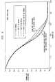
- FIG. 5is a graph of a C-V curve for a capacitor having a high- ⁇ gate dielectric formed under various anneal conditions.
- High- ⁇ dielectric films currently being considered to replace SiONare typically deposited oxides or nitrides such as HfSiO, HfSiON, AlON, or AlZrO.
- Deposition techniquessuch as CVD (chemical vapor deposition), PVD (physical vapor deposition), ALD (atomic layer deposition), and MBE (molecular beam epitaxy) may be used to form these films.
- the macroscopic composition (e.g., metal:Si ratio) of the filmsis reasonably easy to control during fabrication, but the defect content (e.g., point defects like oxygen vacancies) is usually not.
- unwanted speciessuch as C, CH, OH, CO 3 , etc. can be incorporated into the film. Both point defects as well as unwanted impurities are detrimental to the electrical properties of the dielectric film.
- the filmsmay not be fully densified.
- an oxidizing ambient annealin order to improve the film properties after deposition.
- This annealcan have the effects of reducing defects and ensuring that the film has the correct amount of oxygen. Additionally, for CVD films, this oxidation anneal can help to remove carbon and/or OH from the film. This effect is expected to result in reduced leakage currents and possibly improved interface characteristics.
- this oxidizing annealcan also cause the growth of a lower dielectric-constant layer (primarily made up of SiO 2 ) between the high- ⁇ gate material and the Si substrate.
- Low temperature oxidizing annealsavoid increases in the EOT (effective oxide thickness) but does not allow for densification.
- Non-oxidizing (e.g., Ar, He or N 2 ) high temperature annealsallow for densification but typically do not heal defects or adjust for non-stoiciometry.
- the current inventionprovides a means to use the oxidation anneals to heal defects and improve the film properties while at the same time preventing the formation of unwanted lower dielectric constant interface layers.
- An embodiment of the inventionuses a two-step anneal wherein the first step is a high temperature anneal in a non-oxidizing ambient and the second step is a low temperature oxidizing anneal.
- a semiconductor body 100is processed through the formation of isolation structures 102 .
- a high- ⁇ gate dielectric 104is formed at the surface of semiconductor body 100 .
- High- ⁇ dielectric 104may, for example, comprise a deposited metal-nitride, metal-oxide or metal-oxynitride such as MN, MO, MON. MStO, MSiN, MSiON, MAIO, MAIN, MAION, MAISIO, MAISIN, or MAISION, where M Is Zr, Hf, La, Y, GD, Eu, Pr, or Ce.
- high- ⁇ gate dielectric 104is subjected to a first anneal.
- the first annealoccurs in a non-oxidizing ambient 106 .
- the non-oxidizing ambient 106may, for example, comprise N 2 .
- Other inert ambientssuch as Ar or He may alternatively be used.
- the first annealis a higher temperature anneal, preferably in the range of 700° C. to 1100° C.
- the first annealmay be performed at 1000° C. in a N 2 ambient for 60 sec.
- the purpose of the first annealis to densify the high- ⁇ gate dielectric 104 .
- high- ⁇ dielectric 104is subjected to a second (mild oxidation) anneal to heal the film and interface defects.
- the second annealoccurs in an oxidizing ambient 108 .
- the oxidizing ambient 108may, for example, comprise O 2 .
- Other examplesinclude N 2 O, NO, ozone, UV O 2 , and H 2 O 2 .
- the second annealis a lower temperature anneal and may be a thermal anneal, with or without UV exposure, or a low temperature plasma process.
- the lower temperatureis not greater than that of the first anneal (e.g., room temperature to 1000° C.).
- the temperature, time and pressure of the second annealare chosen so as not to significantly increase the EOT.
- the oxidizer partial pressuremay be in the range of mTorr to 1 atm.
- the second annealmay be performed at 700° C. in O 2 for 60 sec at 1 Torr.
- the first and second annealsmay be separate processes or run as two steps within one recipe. For example, depending on the anneal tool configuration, this dual anneal sequence could be done in a single processing run with a multistep annealing recipe.
- a gate electrode material 110is deposited over the high- ⁇ gate dielectric 104 , as shown in FIG. 4 . Processing then continues by patterning and etching to form the gate electrode, forming the source/drain junction regions, forming interconnects and packaging the device.
- Table I belowshows the EOT and leakage current for various anneals: no anneal (NONE); high temperature non-oxidizing anneal only (1000° C. N 2 ); low temperature oxidizing anneal only at reduced pressure (700° C. O 2 1 Torr); and two step anneal (1000° C. N 2 +700° C. O 2 1 Torr).
- the two step anneal according to the embodiment of the inventionresults in lower leakage current than the unannealed case and reduced leakage current at the same EOT compared to the N 2 anneal only case.
- the two-step annealalso maintains lower EOT than the single O 2 anneal case.
- FIG. 5is a C-V curve for the four conditions of Table I.
- the two-step annealshows the least hump and stretchout due to interface traps.
Landscapes
- Engineering & Computer Science (AREA)
- Microelectronics & Electronic Packaging (AREA)
- Condensed Matter Physics & Semiconductors (AREA)
- General Physics & Mathematics (AREA)
- Manufacturing & Machinery (AREA)
- Computer Hardware Design (AREA)
- Physics & Mathematics (AREA)
- Power Engineering (AREA)
- Chemical & Material Sciences (AREA)
- Chemical Kinetics & Catalysis (AREA)
- Crystallography & Structural Chemistry (AREA)
- General Chemical & Material Sciences (AREA)
- Insulated Gate Type Field-Effect Transistor (AREA)
- Formation Of Insulating Films (AREA)
Abstract
Description
This application claims priority under 35 USC § 119(e)(1) of provisional application No. 60/347,331 filed Jan. 10, 2002.
The invention is generally related to the field of forming high dielectric constant (high-κ) films in semiconductor devices and more specifically to forming high-κ gate dielectrics.
As semiconductor devices have scaled to smaller and smaller dimensions, the gate dielectric thickness has continued to shrink. Although further scaling of devices is still possible, scaling of the gate dielectric thickness has almost reached its practical limit with the conventional gate dielectric material, silicon dioxide. Further scaling of silicon dioxide gate dielectric thickness will involve a host of problems: extremely thin layers allow for large leakage currents due to direct tunneling through the oxide. Because such layers are formed literally from a few layers of atoms, exacting process control is required to repeatably produce such layers. Uniformity of coverage is also critical because device parameters may change dramatically based on the presence or absence of even a single monolayer of dielectric material. Finally, such thin layers form poor diffusion barriers to impurities.
Realizing the limitations of silicon dioxide, researchers have searched for alternative dielectric materials which can be formed in a thicker layer than silicon dioxide and yet still produce the same field effect performance. This performance is often expressed as “equivalent oxide thickness”: although the alternative material layer may be thick, it has the equivalent effect of a much thinner layer of silicon dioxide (commonly called simply “oxide”). In some instances, silicon dioxide has been replaced with a SiON. However, even higher-K dielectrics will soon be needed. Some films currently being investigated include deposited oxides or nitrides such as HfSiO, HfSiON, AlON, and AlZrO. Manufacturable processes for incorporating these materials are needed.
In the drawings:
FIGS. 1-4 are cross-sectional diagrams of a high-κ gate dielectric formed according to an embodiment of the invention at various stages of fabrication; and
FIG. 5 is a graph of a C-V curve for a capacitor having a high-κ gate dielectric formed under various anneal conditions.
High-κ dielectric films currently being considered to replace SiON are typically deposited oxides or nitrides such as HfSiO, HfSiON, AlON, or AlZrO. Deposition techniques such as CVD (chemical vapor deposition), PVD (physical vapor deposition), ALD (atomic layer deposition), and MBE (molecular beam epitaxy) may be used to form these films. The macroscopic composition (e.g., metal:Si ratio) of the films is reasonably easy to control during fabrication, but the defect content (e.g., point defects like oxygen vacancies) is usually not. Additionally, depending upon the deposition type and precursor materials used, unwanted species such as C, CH, OH, CO3, etc. can be incorporated into the film. Both point defects as well as unwanted impurities are detrimental to the electrical properties of the dielectric film. Finally, the films may not be fully densified.
Because of the presence of defects after deposition, it is generally desirable to use an oxidizing ambient anneal in order to improve the film properties after deposition. This anneal can have the effects of reducing defects and ensuring that the film has the correct amount of oxygen. Additionally, for CVD films, this oxidation anneal can help to remove carbon and/or OH from the film. This effect is expected to result in reduced leakage currents and possibly improved interface characteristics. However, this oxidizing anneal can also cause the growth of a lower dielectric-constant layer (primarily made up of SiO2) between the high-κ gate material and the Si substrate. Low temperature oxidizing anneals avoid increases in the EOT (effective oxide thickness) but does not allow for densification. Non-oxidizing (e.g., Ar, He or N2) high temperature anneals allow for densification but typically do not heal defects or adjust for non-stoiciometry.
The current invention provides a means to use the oxidation anneals to heal defects and improve the film properties while at the same time preventing the formation of unwanted lower dielectric constant interface layers. An embodiment of the invention uses a two-step anneal wherein the first step is a high temperature anneal in a non-oxidizing ambient and the second step is a low temperature oxidizing anneal.
The invention will now be described in conjunction with a method for forming a MOSFET transistor. Referring to FIG. 1, asemiconductor body 100 is processed through the formation ofisolation structures 102. A high-κ gate dielectric104 is formed at the surface ofsemiconductor body 100. High-κ dielectric104 may, for example, comprise a deposited metal-nitride, metal-oxide or metal-oxynitride such as MN, MO, MON. MStO, MSiN, MSiON, MAIO, MAIN, MAION, MAISIO, MAISIN, or MAISION, where M Is Zr, Hf, La, Y, GD, Eu, Pr, or Ce. U.S. Pat. Nos. 8,291,886 issued Sep. 18, 2001, 6,291,867 issued Sep. 18, 2001, 6,020,243 issued Feb. 1, 2000, and 6,013,553 issued Jan. 11, 2000, assigned to Texas Instruments Incorporated and Incorporated herein by reference, describe processes for forming Zr or Hf oxynitride and silicon-oxynitride gate dielectrics.
Referring to FIG. 2, high-κ gate dielectric104 is subjected to a first anneal. The first anneal occurs in anon-oxidizing ambient 106. The non-oxidizingambient 106 may, for example, comprise N2. Other inert ambients such as Ar or He may alternatively be used. The first anneal is a higher temperature anneal, preferably in the range of 700° C. to 1100° C. As an example, the first anneal may be performed at 1000° C. in a N2ambient for 60 sec. The purpose of the first anneal is to densify the high-κ gate dielectric104.
Referring to FIG. 3, high-κ dielectric104 is subjected to a second (mild oxidation) anneal to heal the film and interface defects. The second anneal occurs in an oxidizingambient 108. The oxidizingambient 108 may, for example, comprise O2. Other examples include N2O, NO, ozone, UV O2, and H2O2. The second anneal is a lower temperature anneal and may be a thermal anneal, with or without UV exposure, or a low temperature plasma process. The lower temperature is not greater than that of the first anneal (e.g., room temperature to 1000° C.). The temperature, time and pressure of the second anneal are chosen so as not to significantly increase the EOT. Reduced pressure is helpful in avoiding oxide growth (increased EOT). With reduced pressures, higher temperatures can be used. The oxidizer partial pressure may be in the range of mTorr to 1 atm. For example, the second anneal may be performed at 700° C. in O2for 60 sec at 1 Torr.
The first and second anneals may be separate processes or run as two steps within one recipe. For example, depending on the anneal tool configuration, this dual anneal sequence could be done in a single processing run with a multistep annealing recipe.
After the first and second anneals, agate electrode material 110 is deposited over the high-κ gate dielectric104, as shown in FIG.4. Processing then continues by patterning and etching to form the gate electrode, forming the source/drain junction regions, forming interconnects and packaging the device.
Table I below shows the EOT and leakage current for various anneals: no anneal (NONE); high temperature non-oxidizing anneal only (1000° C. N2); low temperature oxidizing anneal only at reduced pressure (700° C. O21 Torr); and two step anneal (1000° C. N2+700° C. O21 Torr). The two step anneal according to the embodiment of the invention results in lower leakage current than the unannealed case and reduced leakage current at the same EOT compared to the N2anneal only case. The two-step anneal also maintains lower EOT than the single O2anneal case.
| TABLE I | ||
| Anneal | EOT (Å) | Jg (A/cm2) |
| None | 13 ± 1.7 | 4.4 ± 0.62 |
| 1000° C. N2 | 13.6 ± 0.54 | 1.3 ± 0.13 |
| 700° C. O21 Torr | 14.5 ± 0.8 | 1.4 ± 0.15 |
| 1000° C. N2+ 700° C. O21 Torr | 13.6 ± 0.4 | 0.7 ± 0.08 |
FIG. 5 is a C-V curve for the four conditions of Table I. There is a significant hump and stretchout for the unannealed and O2single anneal. This is due to interface traps, there is a significant reduction in the hump and stretchout for the N2only anneal, but the best CV curve is for the two-step anneal sequence. The two-step anneal shows the least hump and stretchout due to interface traps.
While this invention has been described with reference to illustrative embodiments, this description is not intended to be construed in a limiting sense. Various modifications and combinations of the illustrative embodiments, as well as other embodiments of the invention, will be apparent to persons skilled in the art upon reference to the description. It is therefore intended that the appended claims encompass any such modifications or embodiments.
Claims (22)
1. A method for fabricating an integrated circuit, comprising the following steps performed in order:
depositing a high-κ gate dielectric over a surface of a semiconductor body, wherein said high-κ gate dielectric comprises a material selected from the group consisting of MN, MO, MON, MSiO, MSiN, MSiON, MAIO, MAIN, MAION, MAISiO, MAISIN, or MAISiON, where M is Zr, Hf, La, Y, Gd, Eu, Pr, or Ce;
performing a first anneal in a non-oxidizing inert ambient to densify the high-κ gate dielectric; and
performing a second anneal in an oxidizing ambient.
2. The method ofclaim 1 , wherein said high-κ gate dielectric comprises a metal oxide.
3. The method ofclaim 1 , wherein said first anneal occurs at a temperature on the order of 1000° C.
4. The method ofclaim 3 , wherein said first anneal occurs in a N2ambient and has a duration on the order of 60 seconds.
5. The method ofclaim 1 , wherein said second anneal occurs at a temperature on the order of 700° C. and has a duration on the order of 60 seconds.
6. The method ofclaim 5 , wherein said second anneal occurs in an O2ambient.
7. The method ofclaim 1 , wherein a partial pressure of oxidizer during said second anneal is in the range of 1 mTorr to 1 atm.
8. The method ofclaim 1 , wherein said second anneal comprises a thermal anneal.
9. The method ofclaim 8 , wherein said thermal anneal is performed with UV exposure.
10. The method ofclaim 1 , wherein said second anneal comprises a low temperature plasma process.
11. A method for fabricating an integrated circuit, comprising the following steps performed in order:
depositing a high-κ gate dielectric over a surface of a semiconductor body, wherein said high-κ gate dielectric comprises a metal oxynitride;
performing a first anneal in a non-oxidizing inert ambient to densify the high-κ oats dielectric; and
performing a second anneal in an oxidizing ambient.
12. A method for fabricating an integrated circuit, comprising the following steps performed in order:
depositing a high-κ gate dielectric over a surface of a semiconductor body, wherein said high-κ gate dielectric comprises a metal-silicon-oxide;
performing a first anneal in a non-oxidizing inert ambient to density the high-κ gate dielectric; and
performing a second anneal in an oxidizing ambient.
13. A method for fabricating an integrated circuit, comprising the following steps performed in order:
depositing a high-κ gate dielectric over a surface of a semiconductor body, wherein said high-κ gate dielectric comprises a metal-silicon-oxynitride;
performing a first anneal in a non-oxidizing inert ambient to density the high-κ gate dielectric; and
performing a second anneal in an oxidizing ambient.
14. A method for fabricating an integrated circuit, comprising the following steps performed in order:
depositing a high-κ gate dielectric over a surface of a semiconductor body;
performing a first anneal in a non-oxidizing inert ambient to density the high-κ gate dielectric; and
performing a second anneal in an oxidizing ambient, wherein said first anneal is a high temperature anneal and the second anneal is a lower temperature anneal, wherein said lower temperature is lower than said high temperature.
15. A method for fabricating an integrated circuit, comprising the steps of:
providing a partially processed semiconductor body;
depositing a high-κ gate dielectric over a surface of the semiconductor body;
performing a first anneal at a temperature of approximately 1000° C. in a non-oxidizing ambient to densify the high-κ gate dielectric;
then, performing a second anneal at a temperature of approximately 7000° C. in an oxidizing ambient to reduce interface defects; and
then, forming a gate electrode material over the high-κ gate dielectric.
16. The method ofclaim 15 wherein said second anneal is performed at reduced pressure.
17. The method ofclaim 15 , wherein said high-κ gate dielectric comprises a metal-silicon-oxide.
18. The method ofclaim 15 , wherein said high-κ gate dielectric comprises a metal-silicon-oxynitride.
19. The method ofclaim 15 , wherein said high-κ gate dielectric comprises a material selected from the group consisting of MN, MO, MON, MSiO, MSIN, MSiON, MAIO, MAIN, MAION, MAISiO, MAISN, or MAISiON, where M is Zr, Hf, La, Y, Gd, Eu, Pr, or Ce.
20. A method for fabricating an integrated circuit, comprising the steps of:
providing a partially processed semiconductor body;
depositing a high-κ gate dielectric over a surface of the semiconductor body, said high-κ gate dielectric comprising a metal-silicon-oxide or metal-silicon-oxynitride;
performing a first anneal at a high temperature in a non-oxidizing ambient to densify the high-κ dielectric;
then, performing a second anneal at a temperature lower than said high temperature in an oxidizing ambient, wherein said second anneal does not significantly increase the effective oxide thickness of said high-κ gate dielectric; and
then, forming a gate electrode material over the high-κ gate dielectric.
21. The method ofclaim 20 , wherein said metal-silicon-oxide comprises HfSiO.
22. The method ofclaim 20 , wherein said metal-silicon-oxynitride comprises HfSiON.
Priority Applications (1)
| Application Number | Priority Date | Filing Date | Title |
|---|---|---|---|
| US10/185,326US6821873B2 (en) | 2002-01-10 | 2002-06-28 | Anneal sequence for high-κ film property optimization |
Applications Claiming Priority (2)
| Application Number | Priority Date | Filing Date | Title |
|---|---|---|---|
| US34733102P | 2002-01-10 | 2002-01-10 | |
| US10/185,326US6821873B2 (en) | 2002-01-10 | 2002-06-28 | Anneal sequence for high-κ film property optimization |
Publications (2)
| Publication Number | Publication Date |
|---|---|
| US20030129817A1 US20030129817A1 (en) | 2003-07-10 |
| US6821873B2true US6821873B2 (en) | 2004-11-23 |
Family
ID=26881044
Family Applications (1)
| Application Number | Title | Priority Date | Filing Date |
|---|---|---|---|
| US10/185,326Expired - LifetimeUS6821873B2 (en) | 2002-01-10 | 2002-06-28 | Anneal sequence for high-κ film property optimization |
Country Status (1)
| Country | Link |
|---|---|
| US (1) | US6821873B2 (en) |
Cited By (54)
| Publication number | Priority date | Publication date | Assignee | Title |
|---|---|---|---|---|
| US20040161934A1 (en)* | 2003-02-14 | 2004-08-19 | Sony Corporation | Method for manufacturing semiconductor device |
| US20040175961A1 (en)* | 2002-06-12 | 2004-09-09 | Christopher Olsen | Two-step post nitridation annealing for lower EOT plasma nitrided gate dielectrics |
| US20040266204A1 (en)* | 2003-06-30 | 2004-12-30 | Kwan-Yong Lim | Method for patterning metal wire in semiconductor device |
| US20050037630A1 (en)* | 2002-09-10 | 2005-02-17 | Seok-Joo Doh | Post thermal treatment methods of forming high dielectric layers over interfacial layers in integrated circuit devices |
| US7026694B2 (en) | 2002-08-15 | 2006-04-11 | Micron Technology, Inc. | Lanthanide doped TiOx dielectric films by plasma oxidation |
| US7084078B2 (en) | 2002-08-29 | 2006-08-01 | Micron Technology, Inc. | Atomic layer deposited lanthanide doped TiOx dielectric films |
| US20060178018A1 (en)* | 2003-03-07 | 2006-08-10 | Applied Materials, Inc. | Silicon oxynitride gate dielectric formation using multiple annealing steps |
| US20060183272A1 (en)* | 2005-02-15 | 2006-08-17 | Micron Technology, Inc. | Atomic layer deposition of Zr3N4/ZrO2 films as gate dielectrics |
| US7135421B2 (en) | 2002-06-05 | 2006-11-14 | Micron Technology, Inc. | Atomic layer-deposited hafnium aluminum oxide |
| US7160577B2 (en) | 2002-05-02 | 2007-01-09 | Micron Technology, Inc. | Methods for atomic-layer deposition of aluminum oxides in integrated circuits |
| US20070010103A1 (en)* | 2005-07-11 | 2007-01-11 | Applied Materials, Inc. | Nitric oxide reoxidation for improved gate leakage reduction of sion gate dielectrics |
| US7183186B2 (en) | 2003-04-22 | 2007-02-27 | Micro Technology, Inc. | Atomic layer deposited ZrTiO4 films |
| US7192892B2 (en) | 2003-03-04 | 2007-03-20 | Micron Technology, Inc. | Atomic layer deposited dielectric layers |
| US7199023B2 (en)* | 2002-08-28 | 2007-04-03 | Micron Technology, Inc. | Atomic layer deposited HfSiON dielectric films wherein each precursor is independendently pulsed |
| US7205218B2 (en) | 2002-06-05 | 2007-04-17 | Micron Technology, Inc. | Method including forming gate dielectrics having multiple lanthanide oxide layers |
| US7235854B2 (en) | 2002-08-15 | 2007-06-26 | Micron Technology, Inc. | Lanthanide doped TiOx dielectric films |
| US20080081487A1 (en)* | 2006-09-29 | 2008-04-03 | Oki Electric Industry Co., Ltd. | Method for fabricating semiconductor element |
| US7390756B2 (en) | 2005-04-28 | 2008-06-24 | Micron Technology, Inc. | Atomic layer deposited zirconium silicon oxide films |
| US7402876B2 (en) | 2002-12-04 | 2008-07-22 | Micron Technology, Inc. | Zr— Sn—Ti—O films |
| US7410668B2 (en) | 2001-03-01 | 2008-08-12 | Micron Technology, Inc. | Methods, systems, and apparatus for uniform chemical-vapor depositions |
| US20080237694A1 (en)* | 2007-03-27 | 2008-10-02 | Michael Specht | Integrated circuit, cell, cell arrangement, method for manufacturing an integrated circuit, method for manufacturing a cell, memory module |
| US7498247B2 (en) | 2005-02-23 | 2009-03-03 | Micron Technology, Inc. | Atomic layer deposition of Hf3N4/HfO2 films as gate dielectrics |
| US20090075434A1 (en)* | 2007-09-14 | 2009-03-19 | Junker Kurt H | Method of removing defects from a dielectric material in a semiconductor |
| US7508648B2 (en) | 2005-02-08 | 2009-03-24 | Micron Technology, Inc. | Atomic layer deposition of Dy doped HfO2 films as gate dielectrics |
| US7511326B2 (en) | 2005-03-29 | 2009-03-31 | Micron Technology, Inc. | ALD of amorphous lanthanide doped TiOx films |
| US20090117750A1 (en)* | 2007-10-30 | 2009-05-07 | Interuniversitair Microelektronica Centrum (Imec) | Methods of Forming a Semiconductor Device |
| US7560395B2 (en) | 2005-01-05 | 2009-07-14 | Micron Technology, Inc. | Atomic layer deposited hafnium tantalum oxide dielectrics |
| US7560793B2 (en) | 2002-05-02 | 2009-07-14 | Micron Technology, Inc. | Atomic layer deposition and conversion |
| US7569500B2 (en) | 2002-06-14 | 2009-08-04 | Applied Materials, Inc. | ALD metal oxide deposition process using direct oxidation |
| US7588988B2 (en) | 2004-08-31 | 2009-09-15 | Micron Technology, Inc. | Method of forming apparatus having oxide films formed using atomic layer deposition |
| US7601649B2 (en) | 2004-08-02 | 2009-10-13 | Micron Technology, Inc. | Zirconium-doped tantalum oxide films |
| US7611959B2 (en) | 2002-12-04 | 2009-11-03 | Micron Technology, Inc. | Zr-Sn-Ti-O films |
| US7645710B2 (en) | 2006-03-09 | 2010-01-12 | Applied Materials, Inc. | Method and apparatus for fabricating a high dielectric constant transistor gate using a low energy plasma system |
| US7662729B2 (en) | 2005-04-28 | 2010-02-16 | Micron Technology, Inc. | Atomic layer deposition of a ruthenium layer to a lanthanide oxide dielectric layer |
| US7678710B2 (en) | 2006-03-09 | 2010-03-16 | Applied Materials, Inc. | Method and apparatus for fabricating a high dielectric constant transistor gate using a low energy plasma system |
| US7709402B2 (en) | 2006-02-16 | 2010-05-04 | Micron Technology, Inc. | Conductive layers for hafnium silicon oxynitride films |
| US7719065B2 (en) | 2004-08-26 | 2010-05-18 | Micron Technology, Inc. | Ruthenium layer for a dielectric layer containing a lanthanide oxide |
| US7728626B2 (en) | 2002-07-08 | 2010-06-01 | Micron Technology, Inc. | Memory utilizing oxide nanolaminates |
| US7837838B2 (en) | 2006-03-09 | 2010-11-23 | Applied Materials, Inc. | Method of fabricating a high dielectric constant transistor gate using a low energy plasma apparatus |
| US7869242B2 (en) | 1999-07-30 | 2011-01-11 | Micron Technology, Inc. | Transmission lines for CMOS integrated circuits |
| US7902018B2 (en) | 2006-09-26 | 2011-03-08 | Applied Materials, Inc. | Fluorine plasma treatment of high-k gate stack for defect passivation |
| US7964514B2 (en) | 2006-03-02 | 2011-06-21 | Applied Materials, Inc. | Multiple nitrogen plasma treatments for thin SiON dielectrics |
| US20110204454A1 (en)* | 2010-02-23 | 2011-08-25 | Texas Instruments Incorporated | Semiconductor device including sion gate dielectric with portions having different nitrogen concentrations |
| US8026161B2 (en) | 2001-08-30 | 2011-09-27 | Micron Technology, Inc. | Highly reliable amorphous high-K gate oxide ZrO2 |
| US8110469B2 (en) | 2005-08-30 | 2012-02-07 | Micron Technology, Inc. | Graded dielectric layers |
| US8119210B2 (en) | 2004-05-21 | 2012-02-21 | Applied Materials, Inc. | Formation of a silicon oxynitride layer on a high-k dielectric material |
| US8125038B2 (en) | 2002-07-30 | 2012-02-28 | Micron Technology, Inc. | Nanolaminates of hafnium oxide and zirconium oxide |
| US8450221B2 (en) | 2010-08-04 | 2013-05-28 | Texas Instruments Incorporated | Method of forming MOS transistors including SiON gate dielectric with enhanced nitrogen concentration at its sidewalls |
| US8501563B2 (en) | 2005-07-20 | 2013-08-06 | Micron Technology, Inc. | Devices with nanocrystals and methods of formation |
| US8658525B2 (en) | 2009-10-07 | 2014-02-25 | Taiwan Semiconductor Manufacturing Company, Ltd. | Methods for a gate replacement process |
| WO2020226857A1 (en)* | 2019-05-03 | 2020-11-12 | Applied Materials, Inc. | Treatments to enhance material structures |
| US11271097B2 (en) | 2019-11-01 | 2022-03-08 | Applied Materials, Inc. | Cap oxidation for FinFET formation |
| US11955332B2 (en) | 2019-05-03 | 2024-04-09 | Applied Materials, Inc. | Treatments to enhance material structures |
| US12249511B2 (en) | 2019-05-03 | 2025-03-11 | Applied Materials, Inc. | Treatments to improve device performance |
Families Citing this family (17)
| Publication number | Priority date | Publication date | Assignee | Title |
|---|---|---|---|---|
| US20030111678A1 (en)* | 2001-12-14 | 2003-06-19 | Luigi Colombo | CVD deposition of M-SION gate dielectrics |
| US6919251B2 (en)* | 2002-07-31 | 2005-07-19 | Texas Instruments Incorporated | Gate dielectric and method |
| US20050124121A1 (en)* | 2003-12-09 | 2005-06-09 | Rotondaro Antonio L. | Anneal of high-k dielectric using NH3 and an oxidizer |
| DE10357756B4 (en)* | 2003-12-10 | 2006-03-09 | Infineon Technologies Ag | Process for the preparation of metal oxynitrides by ALD processes using NO and / or N2O |
| US7135361B2 (en)* | 2003-12-11 | 2006-11-14 | Texas Instruments Incorporated | Method for fabricating transistor gate structures and gate dielectrics thereof |
| US6979623B2 (en)* | 2003-12-17 | 2005-12-27 | Texas Instruments Incorporated | Method for fabricating split gate transistor device having high-k dielectrics |
| US7045431B2 (en)* | 2003-12-17 | 2006-05-16 | Texas Instruments Incorporated | Method for integrating high-k dielectrics in transistor devices |
| JP5054509B2 (en)* | 2004-02-25 | 2012-10-24 | ソワテク | Photodetector |
| JP4849419B2 (en)* | 2005-02-03 | 2012-01-11 | ソイテック | Method for reducing trap density in semiconductor wafers |
| US7407850B2 (en)* | 2005-03-29 | 2008-08-05 | Texas Instruments Incorporated | N+ poly on high-k dielectric for semiconductor devices |
| JP4946145B2 (en)* | 2006-04-13 | 2012-06-06 | 富士通セミコンダクター株式会社 | Manufacturing method of ferroelectric memory |
| US20080050879A1 (en)* | 2006-08-23 | 2008-02-28 | Taiwan Semiconductor Manufacturing Co., Ltd. | Methods of forming metal-containing gate structures |
| US20110256682A1 (en)* | 2010-04-15 | 2011-10-20 | Taiwan Semiconductor Manufacturing Company, Ltd. | Multiple Deposition, Multiple Treatment Dielectric Layer For A Semiconductor Device |
| KR20140003154A (en)* | 2012-06-29 | 2014-01-09 | 에스케이하이닉스 주식회사 | Method for manufacturing semiconductor device |
| CN103943492A (en)* | 2013-01-22 | 2014-07-23 | 中芯国际集成电路制造(上海)有限公司 | Semiconductor device and preparation method thereof |
| KR102271003B1 (en)* | 2014-07-11 | 2021-06-29 | 삼성전자주식회사 | Fabricating method of Semiconductor device |
| CN107305846A (en)* | 2016-04-18 | 2017-10-31 | 中芯国际集成电路制造(上海)有限公司 | A kind of semiconductor devices and preparation method thereof |
Citations (10)
| Publication number | Priority date | Publication date | Assignee | Title |
|---|---|---|---|---|
| US4115914A (en)* | 1976-03-26 | 1978-09-26 | Hughes Aircraft Company | Electrically erasable non-volatile semiconductor memory |
| US5876788A (en)* | 1997-01-16 | 1999-03-02 | International Business Machines Corporation | High dielectric TiO2 -SiN composite films for memory applications |
| US6013553A (en)* | 1997-07-24 | 2000-01-11 | Texas Instruments Incorporated | Zirconium and/or hafnium oxynitride gate dielectric |
| EP0973189A2 (en)* | 1998-07-15 | 2000-01-19 | Texas Instruments Incorporated | A method for gate-stack formation including a high-K dielectric |
| US6162744A (en)* | 1998-02-28 | 2000-12-19 | Micron Technology, Inc. | Method of forming capacitors having high-K oxygen containing capacitor dielectric layers, method of processing high-K oxygen containing dielectric layers, method of forming a DRAM cell having having high-K oxygen containing capacitor dielectric layers |
| US6204203B1 (en)* | 1998-10-14 | 2001-03-20 | Applied Materials, Inc. | Post deposition treatment of dielectric films for interface control |
| US6444592B1 (en)* | 2000-06-20 | 2002-09-03 | International Business Machines Corporation | Interfacial oxidation process for high-k gate dielectric process integration |
| US20020142624A1 (en)* | 2000-09-19 | 2002-10-03 | Mattson Technology, Inc. | Method of forming dielectric films |
| US20030057432A1 (en)* | 1998-12-09 | 2003-03-27 | Mark I. Gardner | Ultrathin high-k gate dielectric with favorable interface properties for improved semiconductor device performance |
| US6562491B1 (en)* | 2001-10-15 | 2003-05-13 | Advanced Micro Devices, Inc. | Preparation of composite high-K dielectrics |
- 2002
- 2002-06-28USUS10/185,326patent/US6821873B2/ennot_activeExpired - Lifetime
Patent Citations (11)
| Publication number | Priority date | Publication date | Assignee | Title |
|---|---|---|---|---|
| US4115914A (en)* | 1976-03-26 | 1978-09-26 | Hughes Aircraft Company | Electrically erasable non-volatile semiconductor memory |
| US5876788A (en)* | 1997-01-16 | 1999-03-02 | International Business Machines Corporation | High dielectric TiO2 -SiN composite films for memory applications |
| US6013553A (en)* | 1997-07-24 | 2000-01-11 | Texas Instruments Incorporated | Zirconium and/or hafnium oxynitride gate dielectric |
| US6020243A (en)* | 1997-07-24 | 2000-02-01 | Texas Instruments Incorporated | Zirconium and/or hafnium silicon-oxynitride gate dielectric |
| US6162744A (en)* | 1998-02-28 | 2000-12-19 | Micron Technology, Inc. | Method of forming capacitors having high-K oxygen containing capacitor dielectric layers, method of processing high-K oxygen containing dielectric layers, method of forming a DRAM cell having having high-K oxygen containing capacitor dielectric layers |
| EP0973189A2 (en)* | 1998-07-15 | 2000-01-19 | Texas Instruments Incorporated | A method for gate-stack formation including a high-K dielectric |
| US6204203B1 (en)* | 1998-10-14 | 2001-03-20 | Applied Materials, Inc. | Post deposition treatment of dielectric films for interface control |
| US20030057432A1 (en)* | 1998-12-09 | 2003-03-27 | Mark I. Gardner | Ultrathin high-k gate dielectric with favorable interface properties for improved semiconductor device performance |
| US6444592B1 (en)* | 2000-06-20 | 2002-09-03 | International Business Machines Corporation | Interfacial oxidation process for high-k gate dielectric process integration |
| US20020142624A1 (en)* | 2000-09-19 | 2002-10-03 | Mattson Technology, Inc. | Method of forming dielectric films |
| US6562491B1 (en)* | 2001-10-15 | 2003-05-13 | Advanced Micro Devices, Inc. | Preparation of composite high-K dielectrics |
Non-Patent Citations (1)
| Title |
|---|
| Milton Ohring, "The Materials Science of Thin Films," Academic Press, San Diego, CA, 1992, pp. 8-9.* |
Cited By (106)
| Publication number | Priority date | Publication date | Assignee | Title |
|---|---|---|---|---|
| US7869242B2 (en) | 1999-07-30 | 2011-01-11 | Micron Technology, Inc. | Transmission lines for CMOS integrated circuits |
| US7410668B2 (en) | 2001-03-01 | 2008-08-12 | Micron Technology, Inc. | Methods, systems, and apparatus for uniform chemical-vapor depositions |
| US8026161B2 (en) | 2001-08-30 | 2011-09-27 | Micron Technology, Inc. | Highly reliable amorphous high-K gate oxide ZrO2 |
| US8652957B2 (en) | 2001-08-30 | 2014-02-18 | Micron Technology, Inc. | High-K gate dielectric oxide |
| US7670646B2 (en) | 2002-05-02 | 2010-03-02 | Micron Technology, Inc. | Methods for atomic-layer deposition |
| US7560793B2 (en) | 2002-05-02 | 2009-07-14 | Micron Technology, Inc. | Atomic layer deposition and conversion |
| US7160577B2 (en) | 2002-05-02 | 2007-01-09 | Micron Technology, Inc. | Methods for atomic-layer deposition of aluminum oxides in integrated circuits |
| US7589029B2 (en) | 2002-05-02 | 2009-09-15 | Micron Technology, Inc. | Atomic layer deposition and conversion |
| US8093638B2 (en) | 2002-06-05 | 2012-01-10 | Micron Technology, Inc. | Systems with a gate dielectric having multiple lanthanide oxide layers |
| US7554161B2 (en) | 2002-06-05 | 2009-06-30 | Micron Technology, Inc. | HfAlO3 films for gate dielectrics |
| US7135421B2 (en) | 2002-06-05 | 2006-11-14 | Micron Technology, Inc. | Atomic layer-deposited hafnium aluminum oxide |
| US7205218B2 (en) | 2002-06-05 | 2007-04-17 | Micron Technology, Inc. | Method including forming gate dielectrics having multiple lanthanide oxide layers |
| US20080090425A9 (en)* | 2002-06-12 | 2008-04-17 | Christopher Olsen | Two-step post nitridation annealing for lower EOT plasma nitrided gate dielectrics |
| US20040175961A1 (en)* | 2002-06-12 | 2004-09-09 | Christopher Olsen | Two-step post nitridation annealing for lower EOT plasma nitrided gate dielectrics |
| US7569501B2 (en) | 2002-06-14 | 2009-08-04 | Applied Materials, Inc. | ALD metal oxide deposition process using direct oxidation |
| US7569500B2 (en) | 2002-06-14 | 2009-08-04 | Applied Materials, Inc. | ALD metal oxide deposition process using direct oxidation |
| US7728626B2 (en) | 2002-07-08 | 2010-06-01 | Micron Technology, Inc. | Memory utilizing oxide nanolaminates |
| US8228725B2 (en) | 2002-07-08 | 2012-07-24 | Micron Technology, Inc. | Memory utilizing oxide nanolaminates |
| US8125038B2 (en) | 2002-07-30 | 2012-02-28 | Micron Technology, Inc. | Nanolaminates of hafnium oxide and zirconium oxide |
| US7439194B2 (en) | 2002-08-15 | 2008-10-21 | Micron Technology, Inc. | Lanthanide doped TiOx dielectric films by plasma oxidation |
| US7235854B2 (en) | 2002-08-15 | 2007-06-26 | Micron Technology, Inc. | Lanthanide doped TiOx dielectric films |
| US7026694B2 (en) | 2002-08-15 | 2006-04-11 | Micron Technology, Inc. | Lanthanide doped TiOx dielectric films by plasma oxidation |
| US7326980B2 (en) | 2002-08-28 | 2008-02-05 | Micron Technology, Inc. | Devices with HfSiON dielectric films which are Hf-O rich |
| US7199023B2 (en)* | 2002-08-28 | 2007-04-03 | Micron Technology, Inc. | Atomic layer deposited HfSiON dielectric films wherein each precursor is independendently pulsed |
| US7388246B2 (en) | 2002-08-29 | 2008-06-17 | Micron Technology, Inc. | Lanthanide doped TiOx dielectric films |
| US7084078B2 (en) | 2002-08-29 | 2006-08-01 | Micron Technology, Inc. | Atomic layer deposited lanthanide doped TiOx dielectric films |
| US20050037630A1 (en)* | 2002-09-10 | 2005-02-17 | Seok-Joo Doh | Post thermal treatment methods of forming high dielectric layers over interfacial layers in integrated circuit devices |
| US7037863B2 (en)* | 2002-09-10 | 2006-05-02 | Samsung Electronics Co., Ltd. | Post thermal treatment methods of forming high dielectric layers over interfacial layers in integrated circuit devices |
| US7402876B2 (en) | 2002-12-04 | 2008-07-22 | Micron Technology, Inc. | Zr— Sn—Ti—O films |
| US7611959B2 (en) | 2002-12-04 | 2009-11-03 | Micron Technology, Inc. | Zr-Sn-Ti-O films |
| US7410917B2 (en) | 2002-12-04 | 2008-08-12 | Micron Technology, Inc. | Atomic layer deposited Zr-Sn-Ti-O films using TiI4 |
| US8445952B2 (en) | 2002-12-04 | 2013-05-21 | Micron Technology, Inc. | Zr-Sn-Ti-O films |
| US20040161934A1 (en)* | 2003-02-14 | 2004-08-19 | Sony Corporation | Method for manufacturing semiconductor device |
| US7192892B2 (en) | 2003-03-04 | 2007-03-20 | Micron Technology, Inc. | Atomic layer deposited dielectric layers |
| US7405454B2 (en) | 2003-03-04 | 2008-07-29 | Micron Technology, Inc. | Electronic apparatus with deposited dielectric layers |
| US20070169696A1 (en)* | 2003-03-07 | 2007-07-26 | Christopher Olsen | Two-step post nitridation annealing for lower eot plasma nitrided gate dielectrics |
| US7429540B2 (en) | 2003-03-07 | 2008-09-30 | Applied Materials, Inc. | Silicon oxynitride gate dielectric formation using multiple annealing steps |
| US20060178018A1 (en)* | 2003-03-07 | 2006-08-10 | Applied Materials, Inc. | Silicon oxynitride gate dielectric formation using multiple annealing steps |
| US7863667B2 (en) | 2003-04-22 | 2011-01-04 | Micron Technology, Inc. | Zirconium titanium oxide films |
| US7183186B2 (en) | 2003-04-22 | 2007-02-27 | Micro Technology, Inc. | Atomic layer deposited ZrTiO4 films |
| US20040266204A1 (en)* | 2003-06-30 | 2004-12-30 | Kwan-Yong Lim | Method for patterning metal wire in semiconductor device |
| US8119210B2 (en) | 2004-05-21 | 2012-02-21 | Applied Materials, Inc. | Formation of a silicon oxynitride layer on a high-k dielectric material |
| US7776762B2 (en) | 2004-08-02 | 2010-08-17 | Micron Technology, Inc. | Zirconium-doped tantalum oxide films |
| US7727905B2 (en) | 2004-08-02 | 2010-06-01 | Micron Technology, Inc. | Zirconium-doped tantalum oxide films |
| US8288809B2 (en) | 2004-08-02 | 2012-10-16 | Micron Technology, Inc. | Zirconium-doped tantalum oxide films |
| US7601649B2 (en) | 2004-08-02 | 2009-10-13 | Micron Technology, Inc. | Zirconium-doped tantalum oxide films |
| US8765616B2 (en) | 2004-08-02 | 2014-07-01 | Micron Technology, Inc. | Zirconium-doped tantalum oxide films |
| US7719065B2 (en) | 2004-08-26 | 2010-05-18 | Micron Technology, Inc. | Ruthenium layer for a dielectric layer containing a lanthanide oxide |
| US8907486B2 (en) | 2004-08-26 | 2014-12-09 | Micron Technology, Inc. | Ruthenium for a dielectric containing a lanthanide |
| US8558325B2 (en) | 2004-08-26 | 2013-10-15 | Micron Technology, Inc. | Ruthenium for a dielectric containing a lanthanide |
| US8541276B2 (en) | 2004-08-31 | 2013-09-24 | Micron Technology, Inc. | Methods of forming an insulating metal oxide |
| US7588988B2 (en) | 2004-08-31 | 2009-09-15 | Micron Technology, Inc. | Method of forming apparatus having oxide films formed using atomic layer deposition |
| US8154066B2 (en) | 2004-08-31 | 2012-04-10 | Micron Technology, Inc. | Titanium aluminum oxide films |
| US7602030B2 (en) | 2005-01-05 | 2009-10-13 | Micron Technology, Inc. | Hafnium tantalum oxide dielectrics |
| US7560395B2 (en) | 2005-01-05 | 2009-07-14 | Micron Technology, Inc. | Atomic layer deposited hafnium tantalum oxide dielectrics |
| US8524618B2 (en) | 2005-01-05 | 2013-09-03 | Micron Technology, Inc. | Hafnium tantalum oxide dielectrics |
| US8278225B2 (en) | 2005-01-05 | 2012-10-02 | Micron Technology, Inc. | Hafnium tantalum oxide dielectrics |
| US8742515B2 (en) | 2005-02-08 | 2014-06-03 | Micron Technology, Inc. | Memory device having a dielectric containing dysprosium doped hafnium oxide |
| US8481395B2 (en) | 2005-02-08 | 2013-07-09 | Micron Technology, Inc. | Methods of forming a dielectric containing dysprosium doped hafnium oxide |
| US7508648B2 (en) | 2005-02-08 | 2009-03-24 | Micron Technology, Inc. | Atomic layer deposition of Dy doped HfO2 films as gate dielectrics |
| US7989285B2 (en) | 2005-02-08 | 2011-08-02 | Micron Technology, Inc. | Method of forming a film containing dysprosium oxide and hafnium oxide using atomic layer deposition |
| US7399666B2 (en) | 2005-02-15 | 2008-07-15 | Micron Technology, Inc. | Atomic layer deposition of Zr3N4/ZrO2 films as gate dielectrics |
| US7423311B2 (en) | 2005-02-15 | 2008-09-09 | Micron Technology, Inc. | Atomic layer deposition of Zr3N4/ZrO2 films as gate dielectrics |
| US20060183272A1 (en)* | 2005-02-15 | 2006-08-17 | Micron Technology, Inc. | Atomic layer deposition of Zr3N4/ZrO2 films as gate dielectrics |
| US7960803B2 (en) | 2005-02-23 | 2011-06-14 | Micron Technology, Inc. | Electronic device having a hafnium nitride and hafnium oxide film |
| US7498247B2 (en) | 2005-02-23 | 2009-03-03 | Micron Technology, Inc. | Atomic layer deposition of Hf3N4/HfO2 films as gate dielectrics |
| US8102013B2 (en) | 2005-03-29 | 2012-01-24 | Micron Technology, Inc. | Lanthanide doped TiOx films |
| US7511326B2 (en) | 2005-03-29 | 2009-03-31 | Micron Technology, Inc. | ALD of amorphous lanthanide doped TiOx films |
| US7662729B2 (en) | 2005-04-28 | 2010-02-16 | Micron Technology, Inc. | Atomic layer deposition of a ruthenium layer to a lanthanide oxide dielectric layer |
| US8084808B2 (en) | 2005-04-28 | 2011-12-27 | Micron Technology, Inc. | Zirconium silicon oxide films |
| US7390756B2 (en) | 2005-04-28 | 2008-06-24 | Micron Technology, Inc. | Atomic layer deposited zirconium silicon oxide films |
| US20070010103A1 (en)* | 2005-07-11 | 2007-01-11 | Applied Materials, Inc. | Nitric oxide reoxidation for improved gate leakage reduction of sion gate dielectrics |
| US8921914B2 (en) | 2005-07-20 | 2014-12-30 | Micron Technology, Inc. | Devices with nanocrystals and methods of formation |
| US8501563B2 (en) | 2005-07-20 | 2013-08-06 | Micron Technology, Inc. | Devices with nanocrystals and methods of formation |
| US9627501B2 (en) | 2005-08-30 | 2017-04-18 | Micron Technology, Inc. | Graded dielectric structures |
| US8110469B2 (en) | 2005-08-30 | 2012-02-07 | Micron Technology, Inc. | Graded dielectric layers |
| US8951903B2 (en) | 2005-08-30 | 2015-02-10 | Micron Technology, Inc. | Graded dielectric structures |
| US8067794B2 (en) | 2006-02-16 | 2011-11-29 | Micron Technology, Inc. | Conductive layers for hafnium silicon oxynitride films |
| US8785312B2 (en) | 2006-02-16 | 2014-07-22 | Micron Technology, Inc. | Conductive layers for hafnium silicon oxynitride |
| US7709402B2 (en) | 2006-02-16 | 2010-05-04 | Micron Technology, Inc. | Conductive layers for hafnium silicon oxynitride films |
| US7964514B2 (en) | 2006-03-02 | 2011-06-21 | Applied Materials, Inc. | Multiple nitrogen plasma treatments for thin SiON dielectrics |
| US7645710B2 (en) | 2006-03-09 | 2010-01-12 | Applied Materials, Inc. | Method and apparatus for fabricating a high dielectric constant transistor gate using a low energy plasma system |
| US7678710B2 (en) | 2006-03-09 | 2010-03-16 | Applied Materials, Inc. | Method and apparatus for fabricating a high dielectric constant transistor gate using a low energy plasma system |
| US7837838B2 (en) | 2006-03-09 | 2010-11-23 | Applied Materials, Inc. | Method of fabricating a high dielectric constant transistor gate using a low energy plasma apparatus |
| CN101416286B (en)* | 2006-04-03 | 2012-12-12 | 应用材料公司 | Silicon oxynitride gate dielectric formation using multiple annealing steps |
| US7902018B2 (en) | 2006-09-26 | 2011-03-08 | Applied Materials, Inc. | Fluorine plasma treatment of high-k gate stack for defect passivation |
| US20080081487A1 (en)* | 2006-09-29 | 2008-04-03 | Oki Electric Industry Co., Ltd. | Method for fabricating semiconductor element |
| US20080237694A1 (en)* | 2007-03-27 | 2008-10-02 | Michael Specht | Integrated circuit, cell, cell arrangement, method for manufacturing an integrated circuit, method for manufacturing a cell, memory module |
| US20090075434A1 (en)* | 2007-09-14 | 2009-03-19 | Junker Kurt H | Method of removing defects from a dielectric material in a semiconductor |
| US7776731B2 (en)* | 2007-09-14 | 2010-08-17 | Freescale Semiconductor, Inc. | Method of removing defects from a dielectric material in a semiconductor |
| US9799523B2 (en) | 2007-10-30 | 2017-10-24 | Taiwan Semiconductor Manufacturing Company, Ltd. | Methods of forming a semiconductor device by thermally treating a cleaned surface of a semiconductor substrate in a non-oxidizing ambient |
| US20090117750A1 (en)* | 2007-10-30 | 2009-05-07 | Interuniversitair Microelektronica Centrum (Imec) | Methods of Forming a Semiconductor Device |
| US9159582B2 (en) | 2007-10-30 | 2015-10-13 | Taiwan Semiconductor Manufacturing Company, Ltd. | Methods of forming a semiconductor device |
| CN101425457B (en)* | 2007-10-30 | 2011-04-06 | 台湾积体电路制造股份有限公司 | Method for forming high dielectric constant gate dielectric material and semiconductor element |
| US8658525B2 (en) | 2009-10-07 | 2014-02-25 | Taiwan Semiconductor Manufacturing Company, Ltd. | Methods for a gate replacement process |
| US20110204454A1 (en)* | 2010-02-23 | 2011-08-25 | Texas Instruments Incorporated | Semiconductor device including sion gate dielectric with portions having different nitrogen concentrations |
| US8748996B2 (en) | 2010-02-23 | 2014-06-10 | Texas Instruments Incorporated | Semiconductor device including SiON gate dielectric with portions having different nitrogen concentrations |
| US8441078B2 (en) | 2010-02-23 | 2013-05-14 | Texas Instruments Incorporated | Semiconductor device including SiON gate dielectric with portions having different nitrogen concentrations |
| US8748992B2 (en) | 2010-08-04 | 2014-06-10 | Texas Instruments Incorporated | MOS transistors including SiON gate dielectric with enhanced nitrogen concentration at its sidewalls |
| US8450221B2 (en) | 2010-08-04 | 2013-05-28 | Texas Instruments Incorporated | Method of forming MOS transistors including SiON gate dielectric with enhanced nitrogen concentration at its sidewalls |
| WO2020226857A1 (en)* | 2019-05-03 | 2020-11-12 | Applied Materials, Inc. | Treatments to enhance material structures |
| US10872763B2 (en) | 2019-05-03 | 2020-12-22 | Applied Materials, Inc. | Treatments to enhance material structures |
| US11955332B2 (en) | 2019-05-03 | 2024-04-09 | Applied Materials, Inc. | Treatments to enhance material structures |
| US11961734B2 (en) | 2019-05-03 | 2024-04-16 | Applied Materials, Inc. | Treatments to enhance material structures |
| US12249511B2 (en) | 2019-05-03 | 2025-03-11 | Applied Materials, Inc. | Treatments to improve device performance |
| US11271097B2 (en) | 2019-11-01 | 2022-03-08 | Applied Materials, Inc. | Cap oxidation for FinFET formation |
Also Published As
| Publication number | Publication date |
|---|---|
| US20030129817A1 (en) | 2003-07-10 |
Similar Documents
| Publication | Publication Date | Title |
|---|---|---|
| US6821873B2 (en) | Anneal sequence for high-κ film property optimization | |
| US6809370B1 (en) | High-k gate dielectric with uniform nitrogen profile and methods for making the same | |
| US7135361B2 (en) | Method for fabricating transistor gate structures and gate dielectrics thereof | |
| US20030111678A1 (en) | CVD deposition of M-SION gate dielectrics | |
| US6020024A (en) | Method for forming high dielectric constant metal oxides | |
| US6291867B1 (en) | Zirconium and/or hafnium silicon-oxynitride gate dielectric | |
| US6552388B2 (en) | Hafnium nitride gate dielectric | |
| US6544875B1 (en) | Chemical vapor deposition of silicate high dielectric constant materials | |
| US8575677B2 (en) | Semiconductor device and its manufacturing method | |
| US7115530B2 (en) | Top surface roughness reduction of high-k dielectric materials using plasma based processes | |
| US6645882B1 (en) | Preparation of composite high-K/standard-K dielectrics for semiconductor devices | |
| US7601578B2 (en) | Defect control in gate dielectrics | |
| US6444592B1 (en) | Interfacial oxidation process for high-k gate dielectric process integration | |
| JP4165076B2 (en) | Semiconductor device having high dielectric constant insulating film | |
| US6503846B1 (en) | Temperature spike for uniform nitridization of ultra-thin silicon dioxide layers in transistor gates | |
| US6548366B2 (en) | Method of two-step annealing of ultra-thin silicon dioxide layers for uniform nitrogen profile | |
| US6610614B2 (en) | Method for uniform nitridization of ultra-thin silicon dioxide layers in transistor gates | |
| US6841439B1 (en) | High permittivity silicate gate dielectric | |
| US7205186B2 (en) | System and method for suppressing oxide formation | |
| KR20020005432A (en) | Doped zirconia, or zirconia-like, dielectric film transistor structure and deposition method for same | |
| CN101409234A (en) | Semiconductor structure and manufacture method thereof | |
| US20070166931A1 (en) | Methods of Manufacturing A Semiconductor Device for Improving the Electrical Characteristics of A Dielectric Film | |
| US8294201B2 (en) | High-k gate dielectric and method of manufacture | |
| US7115461B2 (en) | High permittivity silicate gate dielectric | |
| US20020197886A1 (en) | Method for annealing ultra-thin, high quality gate oxide layers using oxidizer/hydrogen mixtures |
Legal Events
| Date | Code | Title | Description |
|---|---|---|---|
| AS | Assignment | Owner name:TEXAS INSTRUMENTS INCORPORATED, TEXAS Free format text:ASSIGNMENT OF ASSIGNORS INTEREST;ASSIGNORS:VISOKAY, MARK R.;COLOMBO, LUIGI;ROTONDARO, ANTONIO L.P.;REEL/FRAME:013282/0263 Effective date:20020716 | |
| STCF | Information on status: patent grant | Free format text:PATENTED CASE | |
| FPAY | Fee payment | Year of fee payment:4 | |
| FPAY | Fee payment | Year of fee payment:8 | |
| FPAY | Fee payment | Year of fee payment:12 |