US6821851B2 - Method of making ultra thin body vertical replacement gate MOSFET - Google Patents
Method of making ultra thin body vertical replacement gate MOSFETDownload PDFInfo
- Publication number
- US6821851B2 US6821851B2US10/649,140US64914003AUS6821851B2US 6821851 B2US6821851 B2US 6821851B2US 64914003 AUS64914003 AUS 64914003AUS 6821851 B2US6821851 B2US 6821851B2
- Authority
- US
- United States
- Prior art keywords
- layer
- ultra thin
- stack
- trench
- single crystal
- Prior art date
- Legal status (The legal status is an assumption and is not a legal conclusion. Google has not performed a legal analysis and makes no representation as to the accuracy of the status listed.)
- Expired - Lifetime
Links
- 238000004519manufacturing processMethods0.000titleclaimsabstractdescription9
- 239000013078crystalSubstances0.000claimsabstractdescription33
- 239000004065semiconductorSubstances0.000claimsabstractdescription28
- 238000000151depositionMethods0.000claimsabstractdescription24
- 238000000137annealingMethods0.000claimsabstractdescription12
- 239000000463materialSubstances0.000claimsabstractdescription11
- 238000011049fillingMethods0.000claimsabstractdescription6
- 238000000034methodMethods0.000claimsdescription33
- VYPSYNLAJGMNEJ-UHFFFAOYSA-NSilicium dioxideChemical groupO=[Si]=OVYPSYNLAJGMNEJ-UHFFFAOYSA-N0.000claimsdescription13
- 239000002019doping agentSubstances0.000claimsdescription12
- 239000000758substrateSubstances0.000claimsdescription8
- 229910052814silicon oxideInorganic materials0.000claimsdescription7
- 229910000577Silicon-germaniumInorganic materials0.000claimsdescription4
- 229910052710siliconInorganic materials0.000claimsdescription2
- 150000002500ionsChemical class0.000claims7
- 238000001953recrystallisationMethods0.000abstractdescription16
- 230000008569processEffects0.000description9
- 238000000348solid-phase epitaxyMethods0.000description8
- 229910052581Si3N4Inorganic materials0.000description6
- 238000013459approachMethods0.000description5
- 238000005468ion implantationMethods0.000description5
- 229910021420polycrystalline siliconInorganic materials0.000description5
- 229920005591polysiliconPolymers0.000description5
- 238000005530etchingMethods0.000description4
- HQVNEWCFYHHQES-UHFFFAOYSA-Nsilicon nitrideChemical compoundN12[Si]34N5[Si]62N3[Si]51N64HQVNEWCFYHHQES-UHFFFAOYSA-N0.000description4
- 229910052681coesiteInorganic materials0.000description3
- 229910052906cristobaliteInorganic materials0.000description3
- 238000009792diffusion processMethods0.000description3
- 230000000694effectsEffects0.000description3
- 239000012299nitrogen atmosphereSubstances0.000description3
- 239000000377silicon dioxideSubstances0.000description3
- 229910052682stishoviteInorganic materials0.000description3
- 229910052905tridymiteInorganic materials0.000description3
- 238000004140cleaningMethods0.000description2
- 239000003989dielectric materialSubstances0.000description2
- 229910021421monocrystalline siliconInorganic materials0.000description2
- 238000010899nucleationMethods0.000description2
- 230000006911nucleationEffects0.000description2
- 230000003071parasitic effectEffects0.000description2
- ZAMOUSCENKQFHK-UHFFFAOYSA-NChlorine atomChemical compound[Cl]ZAMOUSCENKQFHK-UHFFFAOYSA-N0.000description1
- -1Si3N4) layers 16.4Chemical compound0.000description1
- XUIMIQQOPSSXEZ-UHFFFAOYSA-NSiliconChemical compound[Si]XUIMIQQOPSSXEZ-UHFFFAOYSA-N0.000description1
- 238000003917TEM imageMethods0.000description1
- BOTDANWDWHJENH-UHFFFAOYSA-NTetraethyl orthosilicateChemical compoundCCO[Si](OCC)(OCC)OCCBOTDANWDWHJENH-UHFFFAOYSA-N0.000description1
- 235000011054acetic acidNutrition0.000description1
- 150000001243acetic acidsChemical class0.000description1
- 230000006978adaptationEffects0.000description1
- 229910021417amorphous siliconInorganic materials0.000description1
- 238000010420art techniqueMethods0.000description1
- 230000015572biosynthetic processEffects0.000description1
- 239000000460chlorineSubstances0.000description1
- 229910052801chlorineInorganic materials0.000description1
- 239000002131composite materialSubstances0.000description1
- 238000011109contaminationMethods0.000description1
- 238000002425crystallisationMethods0.000description1
- 230000008025crystallizationEffects0.000description1
- 230000008021depositionEffects0.000description1
- 230000005669field effectEffects0.000description1
- 230000008570general processEffects0.000description1
- CJNBYAVZURUTKZ-UHFFFAOYSA-Nhafnium(IV) oxideInorganic materialsO=[Hf]=OCJNBYAVZURUTKZ-UHFFFAOYSA-N0.000description1
- 239000011810insulating materialSubstances0.000description1
- 230000010354integrationEffects0.000description1
- 238000001459lithographyMethods0.000description1
- 238000002156mixingMethods0.000description1
- 239000000203mixtureSubstances0.000description1
- 150000004767nitridesChemical class0.000description1
- 238000000879optical micrographMethods0.000description1
- 238000000206photolithographyMethods0.000description1
- 238000005498polishingMethods0.000description1
- 238000001289rapid thermal chemical vapour depositionMethods0.000description1
- 239000010703siliconSubstances0.000description1
- 239000000126substanceSubstances0.000description1
Images


Classifications
- H—ELECTRICITY
- H10—SEMICONDUCTOR DEVICES; ELECTRIC SOLID-STATE DEVICES NOT OTHERWISE PROVIDED FOR
- H10D—INORGANIC ELECTRIC SEMICONDUCTOR DEVICES
- H10D84/00—Integrated devices formed in or on semiconductor substrates that comprise only semiconducting layers, e.g. on Si wafers or on GaAs-on-Si wafers
- H10D84/01—Manufacture or treatment
- H10D84/0123—Integrating together multiple components covered by H10D12/00 or H10D30/00, e.g. integrating multiple IGBTs
- H10D84/0126—Integrating together multiple components covered by H10D12/00 or H10D30/00, e.g. integrating multiple IGBTs the components including insulated gates, e.g. IGFETs
- H10D84/016—Integrating together multiple components covered by H10D12/00 or H10D30/00, e.g. integrating multiple IGBTs the components including insulated gates, e.g. IGFETs the components including vertical IGFETs
- H—ELECTRICITY
- H10—SEMICONDUCTOR DEVICES; ELECTRIC SOLID-STATE DEVICES NOT OTHERWISE PROVIDED FOR
- H10D—INORGANIC ELECTRIC SEMICONDUCTOR DEVICES
- H10D84/00—Integrated devices formed in or on semiconductor substrates that comprise only semiconducting layers, e.g. on Si wafers or on GaAs-on-Si wafers
- H10D84/01—Manufacture or treatment
- H10D84/02—Manufacture or treatment characterised by using material-based technologies
- H10D84/03—Manufacture or treatment characterised by using material-based technologies using Group IV technology, e.g. silicon technology or silicon-carbide [SiC] technology
- H10D84/038—Manufacture or treatment characterised by using material-based technologies using Group IV technology, e.g. silicon technology or silicon-carbide [SiC] technology using silicon technology, e.g. SiGe
Definitions
- This inventionrelates to field effect transistors (FETs) and, more particularly, to metal-oxide-semiconductor (MOS) vertical FETs or vertical MOSFETs.
- FETsfield effect transistors
- MOSmetal-oxide-semiconductor
- the vertical replacement gate (VRG) MOSFETprovides precise control of all critical dimensions without lithography, while maintaining the essential features of advanced planar MOSFETs.
- the partially depleted (PD) VRG MOSFETs demonstrated to dateare based on a thick, lithographically defined body. See, for example, J. M. Hergenrother et al., IEDM Tech. Dig ., p. 75 (1999); S-H. Oh et al., IEDM Tech. Dig ., p. 65 (2000); J. M. Hergenrother et al., IEDM Tech. Dig ., p.
- a method of fabricating a VRG MOSFETincludes the steps of: (a) forming a VRG multilayer stack; (b) forming a trench in the stack; (c) depositing an ultra thin, amorphous semiconductor ( ⁇ -semic) layer on the sidewalls of the trench and on the top of the stack (portions of the ultra thin layer on the sidewalls of the trench will ultimately form the channel or ultra thin body (UTB) of the MOSFET); (d) forming a thicker, ⁇ -semic sacrificial layer on the ultra thin layer; (e) annealing the ⁇ -semic layers to recrystallize them into single crystal semiconductor (x-semic) layers; (f) selectively removing the recrystallized sacrificial layer; and (g) performing additional steps to complete the VRG MOSFET.
- the sacrificial layershould facilitate the recrystallization of the ultra thin layer into single crystal material.
- the etch rate of the sacrificial layershould be sufficiently higher than that of the ultra thin layer so that the sacrificial layer can be selectively removed in the presence of the ultra thin layer after recrystallization. The latter condition is illustratively satisfied by doping the sacrificial layer and by not (intentionally) doping the ultra thin layer.
- step (g)includes filling the trench with oxide to form a thick back oxide region
- step (g)includes depositing a thin oxide layer (the back oxide) in the trench and then filling the remainder of the trench with a polycrystalline region (the back gate).
- VRG MOSFETs fabricated in accordance with our inventionare expected to be electrostatically scalable with precise dimensional control. In addition, they can be fully depleted.
- an UTB-VRG-MOSFETincludes an ultra thin x-semic layer disposed on the sidewalls of the trench.
- the ultra thin x-semic layerincludes a pair of UTBs on opposing sidewalls adjacent the gate layer of the VRG stack, source/drain extensions above and below each UTB, and a plug that fills the remainder of the trench.
- the plugis an oxide region (the back oxide); in another embodiment, the plug comprises a thin oxide layer (the back oxide) disposed on the ultra thin layer and a polycrystalline region (the back gate) that fills the remainder of the trench.
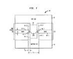
- FIG. 1is a schematic, cross sectional view of a VRG MOSFET in accordance with one embodiment of our invention
- FIGS. 2-4are schematic, cross sectional views depicting a prior art process for fabricating a VRG MOSFET
- FIGS. 5-9are schematic, cross sectional views depicting a process for fabricating a VRG MOSFET in accordance with one aspect of our invention.
- FIG. 10is a schematic, cross sectional view of a VRG MOSFET in accordance with another embodiment of our invention.
- FIGS. 5, 6 , 8 and 9indicate the location of the prior interface between an amorphous layer, later recrystallized into single crystal material, and the single crystal substrate, but in FIGS. 3 and 4 they indicate the location of the top surface of the substrate before the trench was filled with epitaxial material.
- an undoped Si layer grown by CVDtypically has a dopant concentration of about 10 13 -10 15 cm ⁇ 3 .
- a VRG MOSFET 10in accordance with one embodiment of our invention comprises VRG stacks 16 disposed between top and bottom source/drain (S/D) regions 12 and 14 , respectively.
- the two stacksare separated by a trench 18 , which exposes a portion of the substrate 14 and is more clearly seen in FIG. 2 .
- the trench width t Trepresents a lithographic dimension involved in the fabrication of the device.
- Thin single crystal semiconductor (x-semic) layers 14 . 1 , 14 . 2 and 20are formed on the sidewalls of the trench, and a buried oxide region 22 fills the remainder of the trench.
- the buried oxide region 22is known at the back oxide.
- the ultra thin single crystal bodies (UTBs) 20serve as channels that conduct charge between the S/D regions 12 and 14 . They are disposed on opposing sidewalls of the trench and adjacent gate layers 16 . 1 .
- the single crystal layers 14 . 1 and 14 . 2serve as S/D extensions. They are located above and below each of the UTBs.
- Gate dielectrics 16 . 7are located between the gate layers 16 . 1 and the UTBs 20 .
- the ends of the gate layerspenetrate slightly into the UTBs, making the UTBs slightly thinner than the S/D extensions.
- This design featurereferred to as a recessed channel, is well known in the art and has the advantage of reduced parasitic resistance. See, for example, Oh et al., IEDM , p. 65 (2000), which is incorporated herein by reference.
- a VRG MOSFET 100in accordance with an alternative embodiment of our invention comprises VRG stacks 116 disposed between top source region 112 and the bottom drain region 114 .
- the two stacksare separated by a trench similar to the one shown in FIG. 2 .
- Thin x-semic layers 114 . 1 , 114 . 2 and 120are formed on the sidewalls of the trench.
- a thin oxide layer 122known as a back oxide, is deposited over the thin single crystal layers, and a polycrystalline buried region 119 fills the remainder of the trench.
- the buried region 119is known at the back gate, the ultra thin (e.g., ⁇ 30 nm) single crystal bodies (UTBs) 120 serve as channels. They are disposed on opposing sidewalls of the trench and adjacent gate layers 116 . 1 .
- the single crystal layers 114 . 1 and 114 . 2serve as S/D extensions. They are located above and below each of the UTBs.
- Gate dielectrics 116 . 7are located between the gate layers 116 . 1 and the UTBs 120 .
- the ends of the gate layerspenetrate slightly into the UTBs, making the UTBs slightly thinner than the S/D extensions.
- This recessed channel design of FIG. 10also has the advantage of reduced parasitic resistance, as described above in conjunction with the device of FIG. 1 .
- an x-semic layer 14 . 1is also formed on the bottom of the trench, but the single crystal nature of this portion of the layer is not critical from the standpoint of device performance.
- VRG-MOSFETstypically single crystal, polycrystalline, and/or amorphous semiconductors, as well as oxides and/or nitrides of these materials, are used to fabricate VRG-MOSFETs.
- the semiconductorsmay include, for example, Si, SiGe, or Ge.
- the semiconductor materialis Si.
- many of the semiconductor layers of these MOSFETsare single crystal silicon (x-Si), but the top S/D region 12 (FIG. 1) and the source region 112 (FIG. 10) known as a pad layers, are polysilicon.
- the VRG stacks 16 , 116are multilayered, including an undoped silicon oxide layer sandwiched between a pair of doped silicon oxide layers.
- the stacksalso include a plurality of silicon nitride layers that serve as stop etch layers during processing; e.g., a silicon nitride layer is deposited on the top of the stack, and silicon nitride layers are disposed between adjacent oxide layers, as will be explained more fully later in conjunction with the description of FIG. 2 .
- the thickness t Si of the UTBs 20 , 120 and the gate length L Gare defined by deposited thin layers, which enables extremely precise control of these important dimensions.
- Fully depleted UTB devicesshould have a body thickness t Si ⁇ L G /3 to ensure acceptable short-channel control.
- the ultra thin (e.g., ⁇ 20 nm) x-Si layers required for sub-50 nm UTB-VRG devicescannot easily be formed with prior art direct Solid Phase Epitaxy (SPE) techniques, such as those described by V. Subramanian et al. DRC Tech. Dig ., p. 28 (1999), which entails deposition of ⁇ -Si followed by an anneal.
- SPESolid Phase Epitaxy
- SSPESubtractive SPE
- the stack 16includes an undoped silicon oxide (e.g., SiO 2 ) layer 16 . 1 r disposed between doped silicon oxide (e.g., SiO 2 ) layers 16 . 2 and 16 . 3 . Layer 16 .
- undoped silicon oxidee.g., SiO 2
- doped silicon oxidee.g., SiO 2
- Layer 16 . 2is deposited directly on the top surface of substrate 14 , which is typically doped x-Si.
- the oxide layersare interleaved with silicon nitride (e.g., Si 3 N 4 ) layers 16 . 4 , 16 . 5 and 16 . 6 , with the latter being the topmost layer of the stack.
- Suitable photolithography and etching techniquesare then used to form a trench 18 in the stack.
- the trenchhas sufficient depth to expose a portion of the top surface of substrate 14 .
- the prior art processproceeds as shown in FIGS. 3-4; that is, SEG is used to fill the trench 18 with a thick x-Si body 30 .
- Chemical-mechanical polishing (CMP)is then used to planarize the x-Si body so that it is essentially flush with the top of the stack, as shown by body 32 of FIG. 4 .
- CMPchemical-mechanical polishing
- our UTB-VRG processutilizes SSPE to form an ultra thin layer 40 along the sidewalls of the trench and over a portion of the top of the stack, as shown in FIG. 5 .
- Subsequent stepsform region 44 to fill in the remainder of the trench, as shown in FIG. 6 after CMP to planarize the intermediate stage of the device.
- a suitable, thin dielectric layeris desirably formed on the exposed back surface of the layer 40 .
- this dielectricis typically a thermal oxide.
- the thermal oxideensures a high quality interface between the UTBs ( 20 in FIG. 1; 120 in FIG. 10 ), which are formed in layer 40 (FIG. 5 ), and the buried oxide region 22 (FIG. 1) or the back oxide layer 122 (FIG. 10 ), which are formed in region 44 (FIG. 6 ).
- the dielectricmay be formed as a deposited oxide (e.g., SiO 2 , HfO 2 ) or as another insulating material (e.g., Si 3 N 4 ).
- our SSPE techniqueincludes process steps that are illustrated by FIGS. 7-9; that is, (a) depositing an ultra thin first layer 40 . 1 of ⁇ -Si; and then (b) depositing a thicker sacrificial second layer 42 . 1 of ⁇ -Si.
- the sacrificial layerhas two important characteristics: first, its etch rate is sufficiently higher than (e.g., >60:1) that of ultra thin layer 40 . 1 that the sacrificial layer can be selectively removed in the presence of layer 40 . 1 after both have been recrystallized; and second, it should be sufficiently thick to facilitate recrystallization of the ultra thin layer 40 . 1 into single crystal material.
- the ⁇ -Si layerscan formed in a number of different ways, and we have found that rapid thermal CVD is suitable.
- a total thickness of the combination of layers 40 . 1 and 42 . 1 of about 80 nmis suitable, whereas 20 nm is not.
- the minimum thickness of the two layersshould be about 50 nm.
- the sacrificial layershould be at least about 45-30 nm thick to the satisfy the approximate minimum, but would be about 75-60 nm thick for a typical composite thickness of 80 nm.
- the desired differential etch rate (after recrystallization) between the two ⁇ -Si layerscan be realized in a number of ways well known in the art.
- a preferred approachis to dope the two ⁇ -Si layers to sufficiently different levels [e.g., the first layer may be undoped or lightly doped (e.g., with a P dopant concentration as high as about 10 18 cm ⁇ 3 ) and the second layer may be doped to a range of bout 1-4 ⁇ 10 20 cm ⁇ 3 (e.g., with P)].
- This approachworks well with wet chemical etchants such as HNA, which is discussed infra. Other dopants can also be utilized.
- the two ⁇ -Si layersmay be doped with different dopants; e.g., the first ⁇ -Si layer may be doped with B and the second with P.
- a suitable etchantis a dry chlorine-based chemistry.
- the next step (c)is to anneal the amorphous layers 40 . 1 and 42 . 1 so that they recrystallize into single crystal Si.
- the recrystallization front 50(FIG. 8) shows the extent to which the layers are recrystallized; the recrystallized portions of ⁇ -Si layers 40 . 1 and 42 . 1 of FIG. 7 are now x-Si layers 40 . 2 and 42 . 2 in FIG. 8 .
- Various annealing temperature/time parameterscan be used, but we have found an anneal temperature of 575° C. in a nitrogen atmosphere for a few hours to be suitable.
- the next step (d)is to selectively remove both the remaining amorphous portions 40 . 3 and 42 . 3 of layers 40 .
- HNAis highly selective (e.g., 60:1) with respect to the undoped x-Si layer 40 . 2 .
- HNAis a mixture of HF, nitric and acetic acids.
- the next stepsare: (e1) cleaning the back exposed surface of the x-Si layer 40 (FIG. 9) and then preferably growing a thin thermal oxide on it.
- This thermal oxideprovides a good quality interface between the buried oxide 22 and the UTBs 20 , which will be formed from layer 40 ; (f1) depositing a silicon oxide (e.g., TEOS or HDP) to fill the trench and overlay the top of the stack 16 ; (g1) using CMP to planarize the deposited oxide so that it is essentially flush with the top of the stack (cf. FIG.
- a silicon oxidee.g., TEOS or HDP
- the next stepsinclude the following: (e2) cleaning the back exposed surface of the x-Si layer 40 (FIG. 9) and then preferably growing a thin thermal oxide on it.
- This thermal oxideprovides a good quality interface between the back oxide layer 122 and UTBs 120 , which will be formed from layer 40 ; (f2) depositing the thin back oxide layer 122 on the thermal oxide and the top of the stack 16 ; (g2) depositing a thin ⁇ -Si layer on the deposited oxide layer; (h2) using ion implantation to dope the ⁇ -Si layer; dopants of either polarity can be used to adjust the threshold voltage of the device; (i2) depositing an undoped ⁇ -Si region so that it fills the trench and overlays the top of the stack; (The two ⁇ -Si regions will ultimately form the back gate region 119 of the device.) (j2) using CMP to planarize the deposited layers so that the device is essentially flush with the top of the stack
- FIG. 6(k2) if desired, using ion implantation to dope the portions of layer 40 that correspond to the UTBs 20 ; (The ⁇ -Si in the trench also gets doped, but to a negligible degree.) (m2) annealing to cause dopants to diffuse from the adjacent doped oxide layers 16 . 2 and 16 . 3 of the VRG stack (FIG. 2) into the S/D extensions 14 . 1 and 14 . 2 .
- the annealingalso causes the ⁇ -Si in the trench (the back gate region 119 ) to recrystallize into polysilicon and causes the dopants to diffuse nearly uniformly throughout the back gate region.); (n2) depositing an ⁇ -Si pad layer over the top of the stack; and (o2) using ion implantation to dope the pad layer.
- the pad layerserves as the source of the device.
- the doped polysilicon back gate regionis included to further improve scalability (i.e., to reduce undesirable short-channel effects) of the embodiment of FIG. 10 with respect to that of FIG. 1 .
- the VRG processing to complete the MOSFETnext follows the standard VRG fabrication steps described in the Hergenrother ULSI 2001 paper and patent, supra.
- the MOSFETcould be completed by following the process steps associated with, for example, FIGS. 2D-2J of the Hergenrother patent. This subsequent processing causes the ⁇ -Si pad layer to recrystallize into a polycrystalline layer.
- Steps (g2), (h2) and (i2)imply that the end device is intended for CMOS applications. However, if only NMOS or PMOS devices are desired, then these three steps can be consolidated into a single step as follows: depositing a doped ⁇ -Si region that fills the trench and overlaps the top of the stack.
- the UTB-VRG-MOSFET of this examplewas fabricated by first forming a VRG stack and trench as depicted in FIG. 2 . Then, in accordance with this example, an ultra thin (5-20 nm), undoped ⁇ -Si layer 40 . 1 (FIG. 7) was deposited in the trench and on a portion of the top surface of the stack. Next, a relatively thick (70 nm) sacrificial, doped ⁇ -Si layer 42 . 1 was deposited on the ultra thin layer 40 . 1 to facilitate recrystallization into x-Si. The sacrificial layer was doped with P to about 1-4 ⁇ 10 20 cm ⁇ 3 . The stack was then annealed at 575° C.
- the recrystallized (now x-Si) doped and undoped layersare designated 42 . 2 and 40 . 2 , respectively, in FIG. 8 .
- the doped x-Si sacrificial layer 42 . 2was selectively removed with HNA, which had greater than 60:1 selectivity. This selective etching step left behind the undoped x-Si layer 40 , as shown in FIG. 9 .
- HNA etching of the doped layer 42 . 2and a slight overetch to remove an abrupt diffusion tail, left minimal dopant in the remaining film while retaining precise thickness control. Since the diffusion at 575° C. was only a concern while layers 40 . 1 and 42 . 1 remained amorphous ( ⁇ 15 min. based on the measured SPE velocity of >1 ⁇ m/hr.), the above conclusions are quite conservative.
- TEM imagesshowed a 10 nm layer 40 formed by our SSPE technique.
- Convergent-beam diffractionconfirmed that the portion of ultra thin x-Si layer 40 on top of the VRG stack, at a lateral distance of 0.5 ⁇ m on both sides the trench, was single crystal with the same orientation as the substrate 14 .
- These imagesdemonstrated that our SSPE process is capable of creating x-Si layers with high aspect ratio (lateral layer width/final layer thickness; e.g., >200:1) and can provide the ultra thin x-Si needed in the active region of UTB-VRG-MOSFETs.
- our inventiondemonstrates the use of a novel SSPE process can be used to realize a FD-UTB-VRG-MOSFET.
- This MOSFETcombines the excellent electrostatic scalability of UTB devices with a deposition-defined body thickness and gate length, enabling precise control of these important device dimensions.
Landscapes
- Insulated Gate Type Field-Effect Transistor (AREA)
- Thin Film Transistor (AREA)
- Metal-Oxide And Bipolar Metal-Oxide Semiconductor Integrated Circuits (AREA)
Abstract
Description
Claims (15)
Priority Applications (1)
| Application Number | Priority Date | Filing Date | Title |
|---|---|---|---|
| US10/649,140US6821851B2 (en) | 2002-06-06 | 2003-08-27 | Method of making ultra thin body vertical replacement gate MOSFET |
Applications Claiming Priority (2)
| Application Number | Priority Date | Filing Date | Title |
|---|---|---|---|
| US10/164,202US6635924B1 (en) | 2002-06-06 | 2002-06-06 | Ultra thin body vertical replacement gate MOSFET |
| US10/649,140US6821851B2 (en) | 2002-06-06 | 2003-08-27 | Method of making ultra thin body vertical replacement gate MOSFET |
Related Parent Applications (1)
| Application Number | Title | Priority Date | Filing Date |
|---|---|---|---|
| US10/164,202DivisionUS6635924B1 (en) | 2002-06-06 | 2002-06-06 | Ultra thin body vertical replacement gate MOSFET |
Publications (2)
| Publication Number | Publication Date |
|---|---|
| US20040152269A1 US20040152269A1 (en) | 2004-08-05 |
| US6821851B2true US6821851B2 (en) | 2004-11-23 |
Family
ID=28791239
Family Applications (2)
| Application Number | Title | Priority Date | Filing Date |
|---|---|---|---|
| US10/164,202Expired - LifetimeUS6635924B1 (en) | 2002-06-06 | 2002-06-06 | Ultra thin body vertical replacement gate MOSFET |
| US10/649,140Expired - LifetimeUS6821851B2 (en) | 2002-06-06 | 2003-08-27 | Method of making ultra thin body vertical replacement gate MOSFET |
Family Applications Before (1)
| Application Number | Title | Priority Date | Filing Date |
|---|---|---|---|
| US10/164,202Expired - LifetimeUS6635924B1 (en) | 2002-06-06 | 2002-06-06 | Ultra thin body vertical replacement gate MOSFET |
Country Status (1)
| Country | Link |
|---|---|
| US (2) | US6635924B1 (en) |
Cited By (13)
| Publication number | Priority date | Publication date | Assignee | Title |
|---|---|---|---|---|
| US20070167027A1 (en)* | 2006-01-17 | 2007-07-19 | Honeywell International Inc. | System and method for uniform multi-plane silicon oxide layer formation for optical applications |
| US20070252201A1 (en)* | 2006-03-27 | 2007-11-01 | Masaru Kito | Nonvolatile semiconductor memory device and manufacturing method thereof |
| US7454470B1 (en)* | 1999-12-01 | 2008-11-18 | At&T Intellectuall Property Ii, L.P. | System and method for analyzing communications |
| US20120171837A1 (en)* | 2010-12-30 | 2012-07-05 | Samsung Electronics Co., Ltd. | Semiconductor Memory Devices And Methods Of Fabricating The Same |
| US8435845B2 (en) | 2011-04-06 | 2013-05-07 | International Business Machines Corporation | Junction field effect transistor with an epitaxially grown gate structure |
| US20150014816A1 (en)* | 2013-07-12 | 2015-01-15 | Asm Ip Holding B.V. | Doped semiconductor films and processing |
| US9462046B2 (en) | 2003-04-02 | 2016-10-04 | Facebook, Inc. | Degrees of separation for handling communications |
| US9516125B2 (en) | 2003-03-26 | 2016-12-06 | Facebook, Inc. | Identifying and using identities deemed to be known to a user |
| US9727631B2 (en) | 2004-12-20 | 2017-08-08 | Facebook, Inc. | Automatic categorization of entries in a contact list |
| US9882047B2 (en) | 2016-02-01 | 2018-01-30 | International Business Machines Corporation | Self-aligned replacement metal gate spacerless vertical field effect transistor |
| US10341289B2 (en) | 2004-03-05 | 2019-07-02 | Facebook, Inc. | Systems and methods of calculating communications strengths |
| USRE48102E1 (en) | 2002-12-31 | 2020-07-14 | Facebook, Inc. | Implicit population of access control lists |
| US11075280B2 (en) | 2019-04-17 | 2021-07-27 | International Business Machines Corporation | Self-aligned gate and junction for VTFET |
Families Citing this family (14)
| Publication number | Priority date | Publication date | Assignee | Title |
|---|---|---|---|---|
| US7254270B2 (en)* | 2002-07-09 | 2007-08-07 | Hewlett-Packard Development Company, L.P. | System and method for bounding and classifying regions within a graphical image |
| KR100485162B1 (en) | 2003-08-12 | 2005-04-22 | 동부아남반도체 주식회사 | MOS transistor and fabrication method thereof |
| US7259411B1 (en)* | 2003-12-04 | 2007-08-21 | National Semiconductor Corporation | Vertical MOS transistor |
| US7372091B2 (en)* | 2004-01-27 | 2008-05-13 | Micron Technology, Inc. | Selective epitaxy vertical integrated circuit components |
| US7667250B2 (en)* | 2004-07-16 | 2010-02-23 | Aptina Imaging Corporation | Vertical gate device for an image sensor and method of forming the same |
| US7504685B2 (en) | 2005-06-28 | 2009-03-17 | Micron Technology, Inc. | Oxide epitaxial isolation |
| CN102130014B (en)* | 2011-01-05 | 2012-11-07 | 北京大学深圳研究生院 | Method for manufacturing FinFET (field effect transistor) |
| CN120500079A (en) | 2019-08-09 | 2025-08-15 | 美光科技公司 | Transistor and method of forming transistor |
| US11024736B2 (en) | 2019-08-09 | 2021-06-01 | Micron Technology, Inc. | Transistor and methods of forming integrated circuitry |
| US10964811B2 (en)* | 2019-08-09 | 2021-03-30 | Micron Technology, Inc. | Transistor and methods of forming transistors |
| CN111063684B (en)* | 2019-12-06 | 2023-04-11 | 中国科学院微电子研究所 | Semiconductor device having C-shaped active region and electronic apparatus including the same |
| CN111162077B (en)* | 2020-01-02 | 2022-07-22 | 长江存储科技有限责任公司 | Semiconductor structure and forming method thereof |
| US12080553B2 (en)* | 2021-05-13 | 2024-09-03 | Taiwan Semiconductor Manufacturing Co., Ltd. | Semiconductor device and method of manufacture |
| CN114093949B (en)* | 2021-11-01 | 2024-04-26 | 中国科学院微电子研究所 | GIDL-suppressing MOSFET, method of manufacturing the same, and electronic device including the same |
Citations (2)
| Publication number | Priority date | Publication date | Assignee | Title |
|---|---|---|---|---|
| US6020257A (en)* | 1995-06-07 | 2000-02-01 | Elm Technology Corporation | Membrane dielectric isolation IC fabrication |
| US6197641B1 (en)* | 1998-08-28 | 2001-03-06 | Lucent Technologies Inc. | Process for fabricating vertical transistors |
Family Cites Families (1)
| Publication number | Priority date | Publication date | Assignee | Title |
|---|---|---|---|---|
| JPH0797625B2 (en)* | 1986-11-19 | 1995-10-18 | 三菱電機株式会社 | Semiconductor memory device |
- 2002
- 2002-06-06USUS10/164,202patent/US6635924B1/ennot_activeExpired - Lifetime
- 2003
- 2003-08-27USUS10/649,140patent/US6821851B2/ennot_activeExpired - Lifetime
Patent Citations (2)
| Publication number | Priority date | Publication date | Assignee | Title |
|---|---|---|---|---|
| US6020257A (en)* | 1995-06-07 | 2000-02-01 | Elm Technology Corporation | Membrane dielectric isolation IC fabrication |
| US6197641B1 (en)* | 1998-08-28 | 2001-03-06 | Lucent Technologies Inc. | Process for fabricating vertical transistors |
Non-Patent Citations (11)
| Title |
|---|
| Choi et al., Ultra-thin-body SOI MOSFET for Deep-sub-tenth Micron Era, IEEE Electron Dev. Lett., vol. 21, No. 5, p. 254 (May 2000). |
| Dan et al., Lateral solid phase epitaxy of amorphous Si films by selective surface doping method of P atoms, Appl. Phys. Lett., vol. 53, No. 26, p. 2626 (Dec. 1988). |
| Greene et al., Thin Single Crystal Silicon on Oxide by Lateral Solid Phase Epitaxy of Amorphous Silicon and Silicon Germanium, Mat. Res. Soc. Symp. Proc., vol. 609, p. A9.31 (2000). |
| Hergenrother et al, 50 nm Vertical Replacement-Gate (VRG) nMOSFETs with ALD . . . Dielectrics, IEDM Tech. Dig., p. 51 (2001). |
| Hergenrother et al, The Vertical Replacement-Gate . . . Gate Length, IEDM Tech. Dig., p. 75 (1999). |
| Hergenrother et al, The Vertical Replacement-Gate MOSFET, Proc. 2<nd >European Workshop on the Ultimate Integration of Silicon (ULIS)., p. 1 (2001). |
| Hergenrother et al, The Vertical Replacement-Gate MOSFET, Proc. 2nd European Workshop on the Ultimate Integration of Silicon (ULIS)., p. 1 (2001). |
| Ishiwara et al., Lateral solid phase epitaxy in selectively P-doped amorphous Si films, Appl. Phys. Lett., vol. 49, No. 20, p. 1365 (Nov. 1986) (Abstract only). |
| Ishiwara et al., Selective Surface Doping Method of P Atoms in Lateral Solid Phase Epitaxy . . . , Jpn. J. Appl. Phys., vol. 31, p. 1695 (Jun. 1992). |
| Oh et al, 50 nm Vertical Replacement-Gate (VRG) pMOSFETs, IEDM Tech. Dig., p. 65 (2000). |
| Subramanian et al, A Bulk-Si-compatible Ultrathin SOI Technology for sub-100 nm MOSFETs, Device Research Conf. Tech. Dig., p. 28 (1999). |
Cited By (43)
| Publication number | Priority date | Publication date | Assignee | Title |
|---|---|---|---|---|
| US9705834B2 (en) | 1999-12-01 | 2017-07-11 | Facebook, Inc. | System and method for analyzing communications |
| US9185067B1 (en) | 1999-12-01 | 2015-11-10 | Facebook, Inc. | System and method for analyzing communications |
| US9514233B2 (en) | 1999-12-01 | 2016-12-06 | Facebook, Inc. | System and method for analyzing communications |
| US9405843B2 (en) | 1999-12-01 | 2016-08-02 | Facebook, Inc. | System and method for analyzing communications |
| US9619575B2 (en) | 1999-12-01 | 2017-04-11 | Facebook, Inc. | System and method for analyzing communications |
| US9819629B2 (en) | 1999-12-01 | 2017-11-14 | Facebook, Inc. | System and method for analyzing communications |
| US9813370B2 (en) | 1999-12-01 | 2017-11-07 | Facebook, Inc. | System and method for analyzing communications |
| US9749279B2 (en) | 1999-12-01 | 2017-08-29 | Facebook, Inc. | System and method for analyzing communications |
| US9749276B2 (en) | 1999-12-01 | 2017-08-29 | Facebook, Inc. | System and method for analyzing communications |
| US7454470B1 (en)* | 1999-12-01 | 2008-11-18 | At&T Intellectuall Property Ii, L.P. | System and method for analyzing communications |
| USRE48102E1 (en) | 2002-12-31 | 2020-07-14 | Facebook, Inc. | Implicit population of access control lists |
| US9531826B2 (en) | 2003-03-26 | 2016-12-27 | Facebook, Inc. | Managing electronic messages based on inference scores |
| US9736255B2 (en) | 2003-03-26 | 2017-08-15 | Facebook, Inc. | Methods of providing access to messages based on degrees of separation |
| US9516125B2 (en) | 2003-03-26 | 2016-12-06 | Facebook, Inc. | Identifying and using identities deemed to be known to a user |
| US9462046B2 (en) | 2003-04-02 | 2016-10-04 | Facebook, Inc. | Degrees of separation for handling communications |
| US10341289B2 (en) | 2004-03-05 | 2019-07-02 | Facebook, Inc. | Systems and methods of calculating communications strengths |
| US9727631B2 (en) | 2004-12-20 | 2017-08-08 | Facebook, Inc. | Automatic categorization of entries in a contact list |
| US20070167027A1 (en)* | 2006-01-17 | 2007-07-19 | Honeywell International Inc. | System and method for uniform multi-plane silicon oxide layer formation for optical applications |
| US7442589B2 (en)* | 2006-01-17 | 2008-10-28 | Honeywell International Inc. | System and method for uniform multi-plane silicon oxide layer formation for optical applications |
| US9748260B2 (en) | 2006-03-27 | 2017-08-29 | Kabushiki Kaisha Toshiba | Nonvolatile semiconductor memory device and manufacturing method thereof |
| US8551838B2 (en) | 2006-03-27 | 2013-10-08 | Kabushiki Kaisha Toshiba | Nonvolatile semicondutor memory device and manufacturing method thereof |
| US20070252201A1 (en)* | 2006-03-27 | 2007-11-01 | Masaru Kito | Nonvolatile semiconductor memory device and manufacturing method thereof |
| US11903207B2 (en) | 2006-03-27 | 2024-02-13 | Kioxia Corporation | Method for writing data of a first memory cell transistor of a nonvolatile semiconductor memory device |
| US12414299B2 (en) | 2006-03-27 | 2025-09-09 | Kioxia Corporation | Nonvolatile semiconductor memory device and manufacturing method thereof |
| US9064735B2 (en) | 2006-03-27 | 2015-06-23 | Kabushiki Kaisha Toshiba | Nonvolatile semiconductor memory device and manufacturing method thereof |
| US11362106B2 (en) | 2006-03-27 | 2022-06-14 | Kioxia Corporation | Manufacturing method of a nonvolatile semiconductor memory device |
| US7936004B2 (en) | 2006-03-27 | 2011-05-03 | Kabushiki Kaisha Toshiba | Nonvolatile semiconductor memory device and manufacturing method thereof |
| US10916559B2 (en) | 2006-03-27 | 2021-02-09 | Kioxia Corporation | Nonvolatile semiconductor memory device and manufacturing method thereof |
| US11903205B2 (en) | 2006-03-27 | 2024-02-13 | Kioxia Corporation | Method for reading data of a first memory cell transistor of a nonvolatile semiconductor memory device |
| US10211219B2 (en) | 2006-03-27 | 2019-02-19 | Toshiba Memory Corporation | Nonvolatile semiconductor memory device and manufacturing method thereof |
| US11374021B2 (en) | 2006-03-27 | 2022-06-28 | Kioxia Corporation | Manufacturing method of a nonvolatile semiconductor memory device |
| US20120171837A1 (en)* | 2010-12-30 | 2012-07-05 | Samsung Electronics Co., Ltd. | Semiconductor Memory Devices And Methods Of Fabricating The Same |
| US8652897B2 (en)* | 2010-12-30 | 2014-02-18 | Samsung Electronics Co., Ltd. | Semiconductor memory devices and methods of fabricating the same |
| US8435845B2 (en) | 2011-04-06 | 2013-05-07 | International Business Machines Corporation | Junction field effect transistor with an epitaxially grown gate structure |
| US8647936B2 (en) | 2011-04-06 | 2014-02-11 | International Business Machines Corporation | Junction field effect transistor with an epitaxially grown gate structure |
| US9240497B2 (en) | 2011-04-06 | 2016-01-19 | Globalfoundries Inc. | Junction field effect transistor with an epitaxially grown gate structure |
| US20150014816A1 (en)* | 2013-07-12 | 2015-01-15 | Asm Ip Holding B.V. | Doped semiconductor films and processing |
| KR101728377B1 (en) | 2013-07-12 | 2017-04-19 | 에이에스엠 아이피 홀딩 비.브이. | Doped semiconductor films and processing |
| TWI575572B (en)* | 2013-07-12 | 2017-03-21 | Asm Ip控股公司 | Doped semiconductor film and method of forming same |
| US9099423B2 (en)* | 2013-07-12 | 2015-08-04 | Asm Ip Holding B.V. | Doped semiconductor films and processing |
| US10600912B2 (en) | 2016-02-01 | 2020-03-24 | International Business Machines Corporation | Self-aligned replacement metal gate spacerless vertical field effect transistor |
| US9882047B2 (en) | 2016-02-01 | 2018-01-30 | International Business Machines Corporation | Self-aligned replacement metal gate spacerless vertical field effect transistor |
| US11075280B2 (en) | 2019-04-17 | 2021-07-27 | International Business Machines Corporation | Self-aligned gate and junction for VTFET |
Also Published As
| Publication number | Publication date |
|---|---|
| US20040152269A1 (en) | 2004-08-05 |
| US6635924B1 (en) | 2003-10-21 |
Similar Documents
| Publication | Publication Date | Title |
|---|---|---|
| US6821851B2 (en) | Method of making ultra thin body vertical replacement gate MOSFET | |
| US11121215B2 (en) | iFinFET | |
| US9972494B1 (en) | Method and structure to control channel length in vertical FET device | |
| US10658506B2 (en) | Fin cut last method for forming a vertical FinFET device | |
| US6624032B2 (en) | Structure and process flow for fabrication of dual gate floating body integrated MOS transistors | |
| US7241653B2 (en) | Nonplanar device with stress incorporation layer and method of fabrication | |
| US9087921B2 (en) | CMOS with dual raised source and drain for NMOS and PMOS | |
| US9230989B2 (en) | Hybrid CMOS nanowire mesh device and FINFET device | |
| US7078280B2 (en) | Vertical replacement-gate silicon-on-insulator transistor | |
| US8169027B2 (en) | Substrate band gap engineered multi-gate pMOS devices | |
| US7531393B2 (en) | Non-planar MOS structure with a strained channel region | |
| US9053981B2 (en) | Hybrid CMOS nanowire mesh device and PDSOI device | |
| US8563376B2 (en) | Hybrid CMOS nanowire mesh device and bulk CMOS device | |
| US10141448B1 (en) | Vertical FETs with different gate lengths and spacer thicknesses | |
| JP4119663B2 (en) | CMOS structure and fabrication method with non-epitaxial raised source / drain and self-aligned gate | |
| US10410929B2 (en) | Multiple gate length device with self-aligned top junction | |
| TW201115734A (en) | Nanowire mesh FET with multiple threshold voltages | |
| WO2004019414A1 (en) | Tri-gate devices and methods of fabrication | |
| US11295988B2 (en) | Semiconductor FET device with bottom isolation and high-κ first | |
| US10068810B1 (en) | Multiple Fin heights with dielectric isolation | |
| US11205728B2 (en) | Vertical field effect transistor with reduced parasitic capacitance | |
| US8674444B2 (en) | Structure and method of forming a transistor with asymmetric channel and source/drain regions | |
| US10147648B1 (en) | Vertical fin gate structure for RF device | |
| EP1383164A1 (en) | FinFET device and a method for manufacturing such device |
Legal Events
| Date | Code | Title | Description |
|---|---|---|---|
| STCF | Information on status: patent grant | Free format text:PATENTED CASE | |
| FEPP | Fee payment procedure | Free format text:PAYOR NUMBER ASSIGNED (ORIGINAL EVENT CODE: ASPN); ENTITY STATUS OF PATENT OWNER: LARGE ENTITY | |
| FPAY | Fee payment | Year of fee payment:4 | |
| FPAY | Fee payment | Year of fee payment:8 | |
| AS | Assignment | Owner name:DEUTSCHE BANK AG NEW YORK BRANCH, AS COLLATERAL AG Free format text:PATENT SECURITY AGREEMENT;ASSIGNORS:LSI CORPORATION;AGERE SYSTEMS LLC;REEL/FRAME:032856/0031 Effective date:20140506 | |
| AS | Assignment | Owner name:AVAGO TECHNOLOGIES GENERAL IP (SINGAPORE) PTE. LTD Free format text:ASSIGNMENT OF ASSIGNORS INTEREST;ASSIGNOR:AGERE SYSTEMS LLC;REEL/FRAME:035365/0634 Effective date:20140804 | |
| AS | Assignment | Owner name:AGERE SYSTEMS LLC, PENNSYLVANIA Free format text:TERMINATION AND RELEASE OF SECURITY INTEREST IN PATENT RIGHTS (RELEASES RF 032856-0031);ASSIGNOR:DEUTSCHE BANK AG NEW YORK BRANCH, AS COLLATERAL AGENT;REEL/FRAME:037684/0039 Effective date:20160201 Owner name:LSI CORPORATION, CALIFORNIA Free format text:TERMINATION AND RELEASE OF SECURITY INTEREST IN PATENT RIGHTS (RELEASES RF 032856-0031);ASSIGNOR:DEUTSCHE BANK AG NEW YORK BRANCH, AS COLLATERAL AGENT;REEL/FRAME:037684/0039 Effective date:20160201 | |
| AS | Assignment | Owner name:BANK OF AMERICA, N.A., AS COLLATERAL AGENT, NORTH CAROLINA Free format text:PATENT SECURITY AGREEMENT;ASSIGNOR:AVAGO TECHNOLOGIES GENERAL IP (SINGAPORE) PTE. LTD.;REEL/FRAME:037808/0001 Effective date:20160201 Owner name:BANK OF AMERICA, N.A., AS COLLATERAL AGENT, NORTH Free format text:PATENT SECURITY AGREEMENT;ASSIGNOR:AVAGO TECHNOLOGIES GENERAL IP (SINGAPORE) PTE. LTD.;REEL/FRAME:037808/0001 Effective date:20160201 | |
| FPAY | Fee payment | Year of fee payment:12 | |
| AS | Assignment | Owner name:AVAGO TECHNOLOGIES GENERAL IP (SINGAPORE) PTE. LTD., SINGAPORE Free format text:TERMINATION AND RELEASE OF SECURITY INTEREST IN PATENTS;ASSIGNOR:BANK OF AMERICA, N.A., AS COLLATERAL AGENT;REEL/FRAME:041710/0001 Effective date:20170119 Owner name:AVAGO TECHNOLOGIES GENERAL IP (SINGAPORE) PTE. LTD Free format text:TERMINATION AND RELEASE OF SECURITY INTEREST IN PATENTS;ASSIGNOR:BANK OF AMERICA, N.A., AS COLLATERAL AGENT;REEL/FRAME:041710/0001 Effective date:20170119 | |
| AS | Assignment | Owner name:BELL SEMICONDUCTOR, LLC, ILLINOIS Free format text:ASSIGNMENT OF ASSIGNORS INTEREST;ASSIGNORS:AVAGO TECHNOLOGIES GENERAL IP (SINGAPORE) PTE. LTD.;BROADCOM CORPORATION;REEL/FRAME:044886/0001 Effective date:20171208 Owner name:BELL SEMICONDUCTOR, LLC, ILLINOIS Free format text:ASSIGNMENT OF ASSIGNORS INTEREST;ASSIGNORS:AVAGO TECHNOLOGIES GENERAL IP (SINGAPORE) PTE. LTD.;BROADCOM CORPORATION;REEL/FRAME:044886/0608 Effective date:20171208 | |
| AS | Assignment | Owner name:CORTLAND CAPITAL MARKET SERVICES LLC, AS COLLATERA Free format text:SECURITY INTEREST;ASSIGNORS:HILCO PATENT ACQUISITION 56, LLC;BELL SEMICONDUCTOR, LLC;BELL NORTHERN RESEARCH, LLC;REEL/FRAME:045216/0020 Effective date:20180124 | |
| AS | Assignment | Owner name:BELL NORTHERN RESEARCH, LLC, ILLINOIS Free format text:SECURITY INTEREST;ASSIGNOR:CORTLAND CAPITAL MARKET SERVICES LLC;REEL/FRAME:060885/0001 Effective date:20220401 Owner name:BELL SEMICONDUCTOR, LLC, ILLINOIS Free format text:SECURITY INTEREST;ASSIGNOR:CORTLAND CAPITAL MARKET SERVICES LLC;REEL/FRAME:060885/0001 Effective date:20220401 Owner name:HILCO PATENT ACQUISITION 56, LLC, ILLINOIS Free format text:SECURITY INTEREST;ASSIGNOR:CORTLAND CAPITAL MARKET SERVICES LLC;REEL/FRAME:060885/0001 Effective date:20220401 Owner name:BELL NORTHERN RESEARCH, LLC, ILLINOIS Free format text:RELEASE BY SECURED PARTY;ASSIGNOR:CORTLAND CAPITAL MARKET SERVICES LLC;REEL/FRAME:059720/0719 Effective date:20220401 Owner name:BELL SEMICONDUCTOR, LLC, ILLINOIS Free format text:RELEASE BY SECURED PARTY;ASSIGNOR:CORTLAND CAPITAL MARKET SERVICES LLC;REEL/FRAME:059720/0719 Effective date:20220401 Owner name:HILCO PATENT ACQUISITION 56, LLC, ILLINOIS Free format text:RELEASE BY SECURED PARTY;ASSIGNOR:CORTLAND CAPITAL MARKET SERVICES LLC;REEL/FRAME:059720/0719 Effective date:20220401 |