US6821825B2 - Process for deposition of semiconductor films - Google Patents
Process for deposition of semiconductor filmsDownload PDFInfo
- Publication number
- US6821825B2 US6821825B2US10/074,563US7456302AUS6821825B2US 6821825 B2US6821825 B2US 6821825B2US 7456302 AUS7456302 AUS 7456302AUS 6821825 B2US6821825 B2US 6821825B2
- Authority
- US
- United States
- Prior art keywords
- film
- deposition
- trisilane
- temperature
- containing film
- Prior art date
- Legal status (The legal status is an assumption and is not a legal conclusion. Google has not performed a legal analysis and makes no representation as to the accuracy of the status listed.)
- Expired - Lifetime, expires
Links
Images


Classifications
- B—PERFORMING OPERATIONS; TRANSPORTING
- B82—NANOTECHNOLOGY
- B82Y—SPECIFIC USES OR APPLICATIONS OF NANOSTRUCTURES; MEASUREMENT OR ANALYSIS OF NANOSTRUCTURES; MANUFACTURE OR TREATMENT OF NANOSTRUCTURES
- B82Y10/00—Nanotechnology for information processing, storage or transmission, e.g. quantum computing or single electron logic
- H—ELECTRICITY
- H01—ELECTRIC ELEMENTS
- H01L—SEMICONDUCTOR DEVICES NOT COVERED BY CLASS H10
- H01L21/00—Processes or apparatus adapted for the manufacture or treatment of semiconductor or solid state devices or of parts thereof
- H01L21/02—Manufacture or treatment of semiconductor devices or of parts thereof
- H01L21/02104—Forming layers
- H01L21/02107—Forming insulating materials on a substrate
- H01L21/02109—Forming insulating materials on a substrate characterised by the type of layer, e.g. type of material, porous/non-porous, pre-cursors, mixtures or laminates
- H01L21/02112—Forming insulating materials on a substrate characterised by the type of layer, e.g. type of material, porous/non-porous, pre-cursors, mixtures or laminates characterised by the material of the layer
- H01L21/02123—Forming insulating materials on a substrate characterised by the type of layer, e.g. type of material, porous/non-porous, pre-cursors, mixtures or laminates characterised by the material of the layer the material containing silicon
- H01L21/0217—Forming insulating materials on a substrate characterised by the type of layer, e.g. type of material, porous/non-porous, pre-cursors, mixtures or laminates characterised by the material of the layer the material containing silicon the material being a silicon nitride not containing oxygen, e.g. SixNy or SixByNz
- B—PERFORMING OPERATIONS; TRANSPORTING
- B82—NANOTECHNOLOGY
- B82Y—SPECIFIC USES OR APPLICATIONS OF NANOSTRUCTURES; MEASUREMENT OR ANALYSIS OF NANOSTRUCTURES; MANUFACTURE OR TREATMENT OF NANOSTRUCTURES
- B82Y30/00—Nanotechnology for materials or surface science, e.g. nanocomposites
- C—CHEMISTRY; METALLURGY
- C23—COATING METALLIC MATERIAL; COATING MATERIAL WITH METALLIC MATERIAL; CHEMICAL SURFACE TREATMENT; DIFFUSION TREATMENT OF METALLIC MATERIAL; COATING BY VACUUM EVAPORATION, BY SPUTTERING, BY ION IMPLANTATION OR BY CHEMICAL VAPOUR DEPOSITION, IN GENERAL; INHIBITING CORROSION OF METALLIC MATERIAL OR INCRUSTATION IN GENERAL
- C23C—COATING METALLIC MATERIAL; COATING MATERIAL WITH METALLIC MATERIAL; SURFACE TREATMENT OF METALLIC MATERIAL BY DIFFUSION INTO THE SURFACE, BY CHEMICAL CONVERSION OR SUBSTITUTION; COATING BY VACUUM EVAPORATION, BY SPUTTERING, BY ION IMPLANTATION OR BY CHEMICAL VAPOUR DEPOSITION, IN GENERAL
- C23C16/00—Chemical coating by decomposition of gaseous compounds, without leaving reaction products of surface material in the coating, i.e. chemical vapour deposition [CVD] processes
- C23C16/02—Pretreatment of the material to be coated
- C23C16/0272—Deposition of sub-layers, e.g. to promote the adhesion of the main coating
- C—CHEMISTRY; METALLURGY
- C23—COATING METALLIC MATERIAL; COATING MATERIAL WITH METALLIC MATERIAL; CHEMICAL SURFACE TREATMENT; DIFFUSION TREATMENT OF METALLIC MATERIAL; COATING BY VACUUM EVAPORATION, BY SPUTTERING, BY ION IMPLANTATION OR BY CHEMICAL VAPOUR DEPOSITION, IN GENERAL; INHIBITING CORROSION OF METALLIC MATERIAL OR INCRUSTATION IN GENERAL
- C23C—COATING METALLIC MATERIAL; COATING MATERIAL WITH METALLIC MATERIAL; SURFACE TREATMENT OF METALLIC MATERIAL BY DIFFUSION INTO THE SURFACE, BY CHEMICAL CONVERSION OR SUBSTITUTION; COATING BY VACUUM EVAPORATION, BY SPUTTERING, BY ION IMPLANTATION OR BY CHEMICAL VAPOUR DEPOSITION, IN GENERAL
- C23C16/00—Chemical coating by decomposition of gaseous compounds, without leaving reaction products of surface material in the coating, i.e. chemical vapour deposition [CVD] processes
- C23C16/22—Chemical coating by decomposition of gaseous compounds, without leaving reaction products of surface material in the coating, i.e. chemical vapour deposition [CVD] processes characterised by the deposition of inorganic material, other than metallic material
- C23C16/24—Deposition of silicon only
- C—CHEMISTRY; METALLURGY
- C23—COATING METALLIC MATERIAL; COATING MATERIAL WITH METALLIC MATERIAL; CHEMICAL SURFACE TREATMENT; DIFFUSION TREATMENT OF METALLIC MATERIAL; COATING BY VACUUM EVAPORATION, BY SPUTTERING, BY ION IMPLANTATION OR BY CHEMICAL VAPOUR DEPOSITION, IN GENERAL; INHIBITING CORROSION OF METALLIC MATERIAL OR INCRUSTATION IN GENERAL
- C23C—COATING METALLIC MATERIAL; COATING MATERIAL WITH METALLIC MATERIAL; SURFACE TREATMENT OF METALLIC MATERIAL BY DIFFUSION INTO THE SURFACE, BY CHEMICAL CONVERSION OR SUBSTITUTION; COATING BY VACUUM EVAPORATION, BY SPUTTERING, BY ION IMPLANTATION OR BY CHEMICAL VAPOUR DEPOSITION, IN GENERAL
- C23C16/00—Chemical coating by decomposition of gaseous compounds, without leaving reaction products of surface material in the coating, i.e. chemical vapour deposition [CVD] processes
- C23C16/22—Chemical coating by decomposition of gaseous compounds, without leaving reaction products of surface material in the coating, i.e. chemical vapour deposition [CVD] processes characterised by the deposition of inorganic material, other than metallic material
- C23C16/30—Deposition of compounds, mixtures or solid solutions, e.g. borides, carbides, nitrides
- C23C16/308—Oxynitrides
- C—CHEMISTRY; METALLURGY
- C23—COATING METALLIC MATERIAL; COATING MATERIAL WITH METALLIC MATERIAL; CHEMICAL SURFACE TREATMENT; DIFFUSION TREATMENT OF METALLIC MATERIAL; COATING BY VACUUM EVAPORATION, BY SPUTTERING, BY ION IMPLANTATION OR BY CHEMICAL VAPOUR DEPOSITION, IN GENERAL; INHIBITING CORROSION OF METALLIC MATERIAL OR INCRUSTATION IN GENERAL
- C23C—COATING METALLIC MATERIAL; COATING MATERIAL WITH METALLIC MATERIAL; SURFACE TREATMENT OF METALLIC MATERIAL BY DIFFUSION INTO THE SURFACE, BY CHEMICAL CONVERSION OR SUBSTITUTION; COATING BY VACUUM EVAPORATION, BY SPUTTERING, BY ION IMPLANTATION OR BY CHEMICAL VAPOUR DEPOSITION, IN GENERAL
- C23C16/00—Chemical coating by decomposition of gaseous compounds, without leaving reaction products of surface material in the coating, i.e. chemical vapour deposition [CVD] processes
- C23C16/22—Chemical coating by decomposition of gaseous compounds, without leaving reaction products of surface material in the coating, i.e. chemical vapour deposition [CVD] processes characterised by the deposition of inorganic material, other than metallic material
- C23C16/30—Deposition of compounds, mixtures or solid solutions, e.g. borides, carbides, nitrides
- C23C16/32—Carbides
- C23C16/325—Silicon carbide
- C—CHEMISTRY; METALLURGY
- C23—COATING METALLIC MATERIAL; COATING MATERIAL WITH METALLIC MATERIAL; CHEMICAL SURFACE TREATMENT; DIFFUSION TREATMENT OF METALLIC MATERIAL; COATING BY VACUUM EVAPORATION, BY SPUTTERING, BY ION IMPLANTATION OR BY CHEMICAL VAPOUR DEPOSITION, IN GENERAL; INHIBITING CORROSION OF METALLIC MATERIAL OR INCRUSTATION IN GENERAL
- C23C—COATING METALLIC MATERIAL; COATING MATERIAL WITH METALLIC MATERIAL; SURFACE TREATMENT OF METALLIC MATERIAL BY DIFFUSION INTO THE SURFACE, BY CHEMICAL CONVERSION OR SUBSTITUTION; COATING BY VACUUM EVAPORATION, BY SPUTTERING, BY ION IMPLANTATION OR BY CHEMICAL VAPOUR DEPOSITION, IN GENERAL
- C23C16/00—Chemical coating by decomposition of gaseous compounds, without leaving reaction products of surface material in the coating, i.e. chemical vapour deposition [CVD] processes
- C23C16/22—Chemical coating by decomposition of gaseous compounds, without leaving reaction products of surface material in the coating, i.e. chemical vapour deposition [CVD] processes characterised by the deposition of inorganic material, other than metallic material
- C23C16/30—Deposition of compounds, mixtures or solid solutions, e.g. borides, carbides, nitrides
- C23C16/34—Nitrides
- C23C16/345—Silicon nitride
- C—CHEMISTRY; METALLURGY
- C23—COATING METALLIC MATERIAL; COATING MATERIAL WITH METALLIC MATERIAL; CHEMICAL SURFACE TREATMENT; DIFFUSION TREATMENT OF METALLIC MATERIAL; COATING BY VACUUM EVAPORATION, BY SPUTTERING, BY ION IMPLANTATION OR BY CHEMICAL VAPOUR DEPOSITION, IN GENERAL; INHIBITING CORROSION OF METALLIC MATERIAL OR INCRUSTATION IN GENERAL
- C23C—COATING METALLIC MATERIAL; COATING MATERIAL WITH METALLIC MATERIAL; SURFACE TREATMENT OF METALLIC MATERIAL BY DIFFUSION INTO THE SURFACE, BY CHEMICAL CONVERSION OR SUBSTITUTION; COATING BY VACUUM EVAPORATION, BY SPUTTERING, BY ION IMPLANTATION OR BY CHEMICAL VAPOUR DEPOSITION, IN GENERAL
- C23C16/00—Chemical coating by decomposition of gaseous compounds, without leaving reaction products of surface material in the coating, i.e. chemical vapour deposition [CVD] processes
- C23C16/22—Chemical coating by decomposition of gaseous compounds, without leaving reaction products of surface material in the coating, i.e. chemical vapour deposition [CVD] processes characterised by the deposition of inorganic material, other than metallic material
- C23C16/30—Deposition of compounds, mixtures or solid solutions, e.g. borides, carbides, nitrides
- C23C16/36—Carbonitrides
- C—CHEMISTRY; METALLURGY
- C23—COATING METALLIC MATERIAL; COATING MATERIAL WITH METALLIC MATERIAL; CHEMICAL SURFACE TREATMENT; DIFFUSION TREATMENT OF METALLIC MATERIAL; COATING BY VACUUM EVAPORATION, BY SPUTTERING, BY ION IMPLANTATION OR BY CHEMICAL VAPOUR DEPOSITION, IN GENERAL; INHIBITING CORROSION OF METALLIC MATERIAL OR INCRUSTATION IN GENERAL
- C23C—COATING METALLIC MATERIAL; COATING MATERIAL WITH METALLIC MATERIAL; SURFACE TREATMENT OF METALLIC MATERIAL BY DIFFUSION INTO THE SURFACE, BY CHEMICAL CONVERSION OR SUBSTITUTION; COATING BY VACUUM EVAPORATION, BY SPUTTERING, BY ION IMPLANTATION OR BY CHEMICAL VAPOUR DEPOSITION, IN GENERAL
- C23C16/00—Chemical coating by decomposition of gaseous compounds, without leaving reaction products of surface material in the coating, i.e. chemical vapour deposition [CVD] processes
- C23C16/56—After-treatment
- C—CHEMISTRY; METALLURGY
- C30—CRYSTAL GROWTH
- C30B—SINGLE-CRYSTAL GROWTH; UNIDIRECTIONAL SOLIDIFICATION OF EUTECTIC MATERIAL OR UNIDIRECTIONAL DEMIXING OF EUTECTOID MATERIAL; REFINING BY ZONE-MELTING OF MATERIAL; PRODUCTION OF A HOMOGENEOUS POLYCRYSTALLINE MATERIAL WITH DEFINED STRUCTURE; SINGLE CRYSTALS OR HOMOGENEOUS POLYCRYSTALLINE MATERIAL WITH DEFINED STRUCTURE; AFTER-TREATMENT OF SINGLE CRYSTALS OR A HOMOGENEOUS POLYCRYSTALLINE MATERIAL WITH DEFINED STRUCTURE; APPARATUS THEREFOR
- C30B25/00—Single-crystal growth by chemical reaction of reactive gases, e.g. chemical vapour-deposition growth
- C30B25/02—Epitaxial-layer growth
- C—CHEMISTRY; METALLURGY
- C30—CRYSTAL GROWTH
- C30B—SINGLE-CRYSTAL GROWTH; UNIDIRECTIONAL SOLIDIFICATION OF EUTECTIC MATERIAL OR UNIDIRECTIONAL DEMIXING OF EUTECTOID MATERIAL; REFINING BY ZONE-MELTING OF MATERIAL; PRODUCTION OF A HOMOGENEOUS POLYCRYSTALLINE MATERIAL WITH DEFINED STRUCTURE; SINGLE CRYSTALS OR HOMOGENEOUS POLYCRYSTALLINE MATERIAL WITH DEFINED STRUCTURE; AFTER-TREATMENT OF SINGLE CRYSTALS OR A HOMOGENEOUS POLYCRYSTALLINE MATERIAL WITH DEFINED STRUCTURE; APPARATUS THEREFOR
- C30B29/00—Single crystals or homogeneous polycrystalline material with defined structure characterised by the material or by their shape
- C30B29/02—Elements
- C30B29/06—Silicon
- H—ELECTRICITY
- H01—ELECTRIC ELEMENTS
- H01L—SEMICONDUCTOR DEVICES NOT COVERED BY CLASS H10
- H01L21/00—Processes or apparatus adapted for the manufacture or treatment of semiconductor or solid state devices or of parts thereof
- H01L21/02—Manufacture or treatment of semiconductor devices or of parts thereof
- H01L21/02104—Forming layers
- H01L21/02365—Forming inorganic semiconducting materials on a substrate
- H01L21/02367—Substrates
- H01L21/0237—Materials
- H01L21/02422—Non-crystalline insulating materials, e.g. glass, polymers
- H—ELECTRICITY
- H01—ELECTRIC ELEMENTS
- H01L—SEMICONDUCTOR DEVICES NOT COVERED BY CLASS H10
- H01L21/00—Processes or apparatus adapted for the manufacture or treatment of semiconductor or solid state devices or of parts thereof
- H01L21/02—Manufacture or treatment of semiconductor devices or of parts thereof
- H01L21/02104—Forming layers
- H01L21/02365—Forming inorganic semiconducting materials on a substrate
- H01L21/02367—Substrates
- H01L21/02428—Structure
- H01L21/0243—Surface structure
- H—ELECTRICITY
- H01—ELECTRIC ELEMENTS
- H01L—SEMICONDUCTOR DEVICES NOT COVERED BY CLASS H10
- H01L21/00—Processes or apparatus adapted for the manufacture or treatment of semiconductor or solid state devices or of parts thereof
- H01L21/02—Manufacture or treatment of semiconductor devices or of parts thereof
- H01L21/02104—Forming layers
- H01L21/02365—Forming inorganic semiconducting materials on a substrate
- H01L21/02436—Intermediate layers between substrates and deposited layers
- H01L21/02439—Materials
- H01L21/02441—Group 14 semiconducting materials
- H01L21/0245—Silicon, silicon germanium, germanium
- H—ELECTRICITY
- H01—ELECTRIC ELEMENTS
- H01L—SEMICONDUCTOR DEVICES NOT COVERED BY CLASS H10
- H01L21/00—Processes or apparatus adapted for the manufacture or treatment of semiconductor or solid state devices or of parts thereof
- H01L21/02—Manufacture or treatment of semiconductor devices or of parts thereof
- H01L21/02104—Forming layers
- H01L21/02365—Forming inorganic semiconducting materials on a substrate
- H01L21/02436—Intermediate layers between substrates and deposited layers
- H01L21/02494—Structure
- H01L21/02496—Layer structure
- H01L21/0251—Graded layers
- H—ELECTRICITY
- H01—ELECTRIC ELEMENTS
- H01L—SEMICONDUCTOR DEVICES NOT COVERED BY CLASS H10
- H01L21/00—Processes or apparatus adapted for the manufacture or treatment of semiconductor or solid state devices or of parts thereof
- H01L21/02—Manufacture or treatment of semiconductor devices or of parts thereof
- H01L21/02104—Forming layers
- H01L21/02365—Forming inorganic semiconducting materials on a substrate
- H01L21/02518—Deposited layers
- H01L21/02521—Materials
- H01L21/02524—Group 14 semiconducting materials
- H01L21/02529—Silicon carbide
- H—ELECTRICITY
- H01—ELECTRIC ELEMENTS
- H01L—SEMICONDUCTOR DEVICES NOT COVERED BY CLASS H10
- H01L21/00—Processes or apparatus adapted for the manufacture or treatment of semiconductor or solid state devices or of parts thereof
- H01L21/02—Manufacture or treatment of semiconductor devices or of parts thereof
- H01L21/02104—Forming layers
- H01L21/02365—Forming inorganic semiconducting materials on a substrate
- H01L21/02518—Deposited layers
- H01L21/02521—Materials
- H01L21/02524—Group 14 semiconducting materials
- H01L21/02532—Silicon, silicon germanium, germanium
- H—ELECTRICITY
- H01—ELECTRIC ELEMENTS
- H01L—SEMICONDUCTOR DEVICES NOT COVERED BY CLASS H10
- H01L21/00—Processes or apparatus adapted for the manufacture or treatment of semiconductor or solid state devices or of parts thereof
- H01L21/02—Manufacture or treatment of semiconductor devices or of parts thereof
- H01L21/02104—Forming layers
- H01L21/02365—Forming inorganic semiconducting materials on a substrate
- H01L21/02518—Deposited layers
- H01L21/0257—Doping during depositing
- H01L21/02573—Conductivity type
- H01L21/02576—N-type
- H—ELECTRICITY
- H01—ELECTRIC ELEMENTS
- H01L—SEMICONDUCTOR DEVICES NOT COVERED BY CLASS H10
- H01L21/00—Processes or apparatus adapted for the manufacture or treatment of semiconductor or solid state devices or of parts thereof
- H01L21/02—Manufacture or treatment of semiconductor devices or of parts thereof
- H01L21/02104—Forming layers
- H01L21/02365—Forming inorganic semiconducting materials on a substrate
- H01L21/02518—Deposited layers
- H01L21/0257—Doping during depositing
- H01L21/02573—Conductivity type
- H01L21/02579—P-type
- H—ELECTRICITY
- H01—ELECTRIC ELEMENTS
- H01L—SEMICONDUCTOR DEVICES NOT COVERED BY CLASS H10
- H01L21/00—Processes or apparatus adapted for the manufacture or treatment of semiconductor or solid state devices or of parts thereof
- H01L21/02—Manufacture or treatment of semiconductor devices or of parts thereof
- H01L21/02104—Forming layers
- H01L21/02365—Forming inorganic semiconducting materials on a substrate
- H01L21/02518—Deposited layers
- H01L21/02587—Structure
- H01L21/0259—Microstructure
- H01L21/02592—Microstructure amorphous
- H—ELECTRICITY
- H01—ELECTRIC ELEMENTS
- H01L—SEMICONDUCTOR DEVICES NOT COVERED BY CLASS H10
- H01L21/00—Processes or apparatus adapted for the manufacture or treatment of semiconductor or solid state devices or of parts thereof
- H01L21/02—Manufacture or treatment of semiconductor devices or of parts thereof
- H01L21/02104—Forming layers
- H01L21/02365—Forming inorganic semiconducting materials on a substrate
- H01L21/02518—Deposited layers
- H01L21/02587—Structure
- H01L21/0259—Microstructure
- H01L21/02595—Microstructure polycrystalline
- H—ELECTRICITY
- H01—ELECTRIC ELEMENTS
- H01L—SEMICONDUCTOR DEVICES NOT COVERED BY CLASS H10
- H01L21/00—Processes or apparatus adapted for the manufacture or treatment of semiconductor or solid state devices or of parts thereof
- H01L21/02—Manufacture or treatment of semiconductor devices or of parts thereof
- H01L21/02104—Forming layers
- H01L21/02365—Forming inorganic semiconducting materials on a substrate
- H01L21/02518—Deposited layers
- H01L21/02587—Structure
- H01L21/0259—Microstructure
- H01L21/02598—Microstructure monocrystalline
- H—ELECTRICITY
- H01—ELECTRIC ELEMENTS
- H01L—SEMICONDUCTOR DEVICES NOT COVERED BY CLASS H10
- H01L21/00—Processes or apparatus adapted for the manufacture or treatment of semiconductor or solid state devices or of parts thereof
- H01L21/02—Manufacture or treatment of semiconductor devices or of parts thereof
- H01L21/02104—Forming layers
- H01L21/02365—Forming inorganic semiconducting materials on a substrate
- H01L21/02612—Formation types
- H01L21/02617—Deposition types
- H01L21/0262—Reduction or decomposition of gaseous compounds, e.g. CVD
- H—ELECTRICITY
- H01—ELECTRIC ELEMENTS
- H01L—SEMICONDUCTOR DEVICES NOT COVERED BY CLASS H10
- H01L21/00—Processes or apparatus adapted for the manufacture or treatment of semiconductor or solid state devices or of parts thereof
- H01L21/02—Manufacture or treatment of semiconductor devices or of parts thereof
- H01L21/04—Manufacture or treatment of semiconductor devices or of parts thereof the devices having potential barriers, e.g. a PN junction, depletion layer or carrier concentration layer
- H01L21/18—Manufacture or treatment of semiconductor devices or of parts thereof the devices having potential barriers, e.g. a PN junction, depletion layer or carrier concentration layer the devices having semiconductor bodies comprising elements of Group IV of the Periodic Table or AIIIBV compounds with or without impurities, e.g. doping materials
- H01L21/22—Diffusion of impurity materials, e.g. doping materials, electrode materials, into or out of a semiconductor body, or between semiconductor regions; Interactions between two or more impurities; Redistribution of impurities
- H01L21/225—Diffusion of impurity materials, e.g. doping materials, electrode materials, into or out of a semiconductor body, or between semiconductor regions; Interactions between two or more impurities; Redistribution of impurities using diffusion into or out of a solid from or into a solid phase, e.g. a doped oxide layer
- H01L21/2251—Diffusion into or out of group IV semiconductors
- H01L21/2254—Diffusion into or out of group IV semiconductors from or through or into an applied layer, e.g. photoresist, nitrides
- H01L21/2257—Diffusion into or out of group IV semiconductors from or through or into an applied layer, e.g. photoresist, nitrides the applied layer being silicon or silicide or SIPOS, e.g. polysilicon, porous silicon
- H—ELECTRICITY
- H01—ELECTRIC ELEMENTS
- H01L—SEMICONDUCTOR DEVICES NOT COVERED BY CLASS H10
- H01L21/00—Processes or apparatus adapted for the manufacture or treatment of semiconductor or solid state devices or of parts thereof
- H01L21/02—Manufacture or treatment of semiconductor devices or of parts thereof
- H01L21/04—Manufacture or treatment of semiconductor devices or of parts thereof the devices having potential barriers, e.g. a PN junction, depletion layer or carrier concentration layer
- H01L21/18—Manufacture or treatment of semiconductor devices or of parts thereof the devices having potential barriers, e.g. a PN junction, depletion layer or carrier concentration layer the devices having semiconductor bodies comprising elements of Group IV of the Periodic Table or AIIIBV compounds with or without impurities, e.g. doping materials
- H01L21/28—Manufacture of electrodes on semiconductor bodies using processes or apparatus not provided for in groups H01L21/20 - H01L21/268
- H01L21/28008—Making conductor-insulator-semiconductor electrodes
- H01L21/28017—Making conductor-insulator-semiconductor electrodes the insulator being formed after the semiconductor body, the semiconductor being silicon
- H01L21/28026—Making conductor-insulator-semiconductor electrodes the insulator being formed after the semiconductor body, the semiconductor being silicon characterised by the conductor
- H01L21/28035—Making conductor-insulator-semiconductor electrodes the insulator being formed after the semiconductor body, the semiconductor being silicon characterised by the conductor the final conductor layer next to the insulator being silicon, e.g. polysilicon, with or without impurities
- H01L21/28044—Making conductor-insulator-semiconductor electrodes the insulator being formed after the semiconductor body, the semiconductor being silicon characterised by the conductor the final conductor layer next to the insulator being silicon, e.g. polysilicon, with or without impurities the conductor comprising at least another non-silicon conductive layer
- H—ELECTRICITY
- H01—ELECTRIC ELEMENTS
- H01L—SEMICONDUCTOR DEVICES NOT COVERED BY CLASS H10
- H01L21/00—Processes or apparatus adapted for the manufacture or treatment of semiconductor or solid state devices or of parts thereof
- H01L21/02—Manufacture or treatment of semiconductor devices or of parts thereof
- H01L21/04—Manufacture or treatment of semiconductor devices or of parts thereof the devices having potential barriers, e.g. a PN junction, depletion layer or carrier concentration layer
- H01L21/18—Manufacture or treatment of semiconductor devices or of parts thereof the devices having potential barriers, e.g. a PN junction, depletion layer or carrier concentration layer the devices having semiconductor bodies comprising elements of Group IV of the Periodic Table or AIIIBV compounds with or without impurities, e.g. doping materials
- H01L21/28—Manufacture of electrodes on semiconductor bodies using processes or apparatus not provided for in groups H01L21/20 - H01L21/268
- H01L21/28008—Making conductor-insulator-semiconductor electrodes
- H01L21/28017—Making conductor-insulator-semiconductor electrodes the insulator being formed after the semiconductor body, the semiconductor being silicon
- H01L21/28158—Making the insulator
- H01L21/28167—Making the insulator on single crystalline silicon, e.g. using a liquid, i.e. chemical oxidation
- H01L21/28194—Making the insulator on single crystalline silicon, e.g. using a liquid, i.e. chemical oxidation by deposition, e.g. evaporation, ALD, CVD, sputtering, laser deposition
- H—ELECTRICITY
- H01—ELECTRIC ELEMENTS
- H01L—SEMICONDUCTOR DEVICES NOT COVERED BY CLASS H10
- H01L21/00—Processes or apparatus adapted for the manufacture or treatment of semiconductor or solid state devices or of parts thereof
- H01L21/02—Manufacture or treatment of semiconductor devices or of parts thereof
- H01L21/04—Manufacture or treatment of semiconductor devices or of parts thereof the devices having potential barriers, e.g. a PN junction, depletion layer or carrier concentration layer
- H01L21/18—Manufacture or treatment of semiconductor devices or of parts thereof the devices having potential barriers, e.g. a PN junction, depletion layer or carrier concentration layer the devices having semiconductor bodies comprising elements of Group IV of the Periodic Table or AIIIBV compounds with or without impurities, e.g. doping materials
- H01L21/28—Manufacture of electrodes on semiconductor bodies using processes or apparatus not provided for in groups H01L21/20 - H01L21/268
- H01L21/283—Deposition of conductive or insulating materials for electrodes conducting electric current
- H01L21/285—Deposition of conductive or insulating materials for electrodes conducting electric current from a gas or vapour, e.g. condensation
- H01L21/28506—Deposition of conductive or insulating materials for electrodes conducting electric current from a gas or vapour, e.g. condensation of conductive layers
- H01L21/28512—Deposition of conductive or insulating materials for electrodes conducting electric current from a gas or vapour, e.g. condensation of conductive layers on semiconductor bodies comprising elements of Group IV of the Periodic Table
- H01L21/28525—Deposition of conductive or insulating materials for electrodes conducting electric current from a gas or vapour, e.g. condensation of conductive layers on semiconductor bodies comprising elements of Group IV of the Periodic Table the conductive layers comprising semiconducting material
- H—ELECTRICITY
- H01—ELECTRIC ELEMENTS
- H01L—SEMICONDUCTOR DEVICES NOT COVERED BY CLASS H10
- H01L21/00—Processes or apparatus adapted for the manufacture or treatment of semiconductor or solid state devices or of parts thereof
- H01L21/02—Manufacture or treatment of semiconductor devices or of parts thereof
- H01L21/04—Manufacture or treatment of semiconductor devices or of parts thereof the devices having potential barriers, e.g. a PN junction, depletion layer or carrier concentration layer
- H01L21/18—Manufacture or treatment of semiconductor devices or of parts thereof the devices having potential barriers, e.g. a PN junction, depletion layer or carrier concentration layer the devices having semiconductor bodies comprising elements of Group IV of the Periodic Table or AIIIBV compounds with or without impurities, e.g. doping materials
- H01L21/28—Manufacture of electrodes on semiconductor bodies using processes or apparatus not provided for in groups H01L21/20 - H01L21/268
- H01L21/283—Deposition of conductive or insulating materials for electrodes conducting electric current
- H01L21/285—Deposition of conductive or insulating materials for electrodes conducting electric current from a gas or vapour, e.g. condensation
- H01L21/28506—Deposition of conductive or insulating materials for electrodes conducting electric current from a gas or vapour, e.g. condensation of conductive layers
- H01L21/28512—Deposition of conductive or insulating materials for electrodes conducting electric current from a gas or vapour, e.g. condensation of conductive layers on semiconductor bodies comprising elements of Group IV of the Periodic Table
- H01L21/28556—Deposition of conductive or insulating materials for electrodes conducting electric current from a gas or vapour, e.g. condensation of conductive layers on semiconductor bodies comprising elements of Group IV of the Periodic Table by chemical means, e.g. CVD, LPCVD, PECVD, laser CVD
- H—ELECTRICITY
- H01—ELECTRIC ELEMENTS
- H01L—SEMICONDUCTOR DEVICES NOT COVERED BY CLASS H10
- H01L21/00—Processes or apparatus adapted for the manufacture or treatment of semiconductor or solid state devices or of parts thereof
- H01L21/02—Manufacture or treatment of semiconductor devices or of parts thereof
- H01L21/04—Manufacture or treatment of semiconductor devices or of parts thereof the devices having potential barriers, e.g. a PN junction, depletion layer or carrier concentration layer
- H01L21/18—Manufacture or treatment of semiconductor devices or of parts thereof the devices having potential barriers, e.g. a PN junction, depletion layer or carrier concentration layer the devices having semiconductor bodies comprising elements of Group IV of the Periodic Table or AIIIBV compounds with or without impurities, e.g. doping materials
- H01L21/30—Treatment of semiconductor bodies using processes or apparatus not provided for in groups H01L21/20 - H01L21/26
- H01L21/31—Treatment of semiconductor bodies using processes or apparatus not provided for in groups H01L21/20 - H01L21/26 to form insulating layers thereon, e.g. for masking or by using photolithographic techniques; After treatment of these layers; Selection of materials for these layers
- H01L21/3205—Deposition of non-insulating-, e.g. conductive- or resistive-, layers on insulating layers; After-treatment of these layers
- H01L21/32055—Deposition of semiconductive layers, e.g. poly - or amorphous silicon layers
- H—ELECTRICITY
- H10—SEMICONDUCTOR DEVICES; ELECTRIC SOLID-STATE DEVICES NOT OTHERWISE PROVIDED FOR
- H10D—INORGANIC ELECTRIC SEMICONDUCTOR DEVICES
- H10D1/00—Resistors, capacitors or inductors
- H10D1/01—Manufacture or treatment
- H10D1/045—Manufacture or treatment of capacitors having potential barriers, e.g. varactors
- H10D1/047—Manufacture or treatment of capacitors having potential barriers, e.g. varactors of conductor-insulator-semiconductor capacitors, e.g. trench capacitors
- H—ELECTRICITY
- H10—SEMICONDUCTOR DEVICES; ELECTRIC SOLID-STATE DEVICES NOT OTHERWISE PROVIDED FOR
- H10D—INORGANIC ELECTRIC SEMICONDUCTOR DEVICES
- H10D1/00—Resistors, capacitors or inductors
- H10D1/60—Capacitors
- H10D1/68—Capacitors having no potential barriers
- H10D1/692—Electrodes
- H10D1/711—Electrodes having non-planar surfaces, e.g. formed by texturisation
- H10D1/712—Electrodes having non-planar surfaces, e.g. formed by texturisation being rough surfaces, e.g. using hemispherical grains
- H—ELECTRICITY
- H10—SEMICONDUCTOR DEVICES; ELECTRIC SOLID-STATE DEVICES NOT OTHERWISE PROVIDED FOR
- H10D—INORGANIC ELECTRIC SEMICONDUCTOR DEVICES
- H10D10/00—Bipolar junction transistors [BJT]
- H10D10/01—Manufacture or treatment
- H10D10/021—Manufacture or treatment of heterojunction BJTs [HBT]
- H—ELECTRICITY
- H10—SEMICONDUCTOR DEVICES; ELECTRIC SOLID-STATE DEVICES NOT OTHERWISE PROVIDED FOR
- H10D—INORGANIC ELECTRIC SEMICONDUCTOR DEVICES
- H10D62/00—Semiconductor bodies, or regions thereof, of devices having potential barriers
- H10D62/80—Semiconductor bodies, or regions thereof, of devices having potential barriers characterised by the materials
- H10D62/81—Semiconductor bodies, or regions thereof, of devices having potential barriers characterised by the materials of structures exhibiting quantum-confinement effects, e.g. single quantum wells; of structures having periodic or quasi-periodic potential variation
- H10D62/812—Single quantum well structures
- H10D62/814—Quantum box structures
- H—ELECTRICITY
- H10—SEMICONDUCTOR DEVICES; ELECTRIC SOLID-STATE DEVICES NOT OTHERWISE PROVIDED FOR
- H10D—INORGANIC ELECTRIC SEMICONDUCTOR DEVICES
- H10D64/00—Electrodes of devices having potential barriers
- H10D64/60—Electrodes characterised by their materials
- H10D64/66—Electrodes having a conductor capacitively coupled to a semiconductor by an insulator, e.g. MIS electrodes
- H10D64/68—Electrodes having a conductor capacitively coupled to a semiconductor by an insulator, e.g. MIS electrodes characterised by the insulator, e.g. by the gate insulator
- H10D64/691—Electrodes having a conductor capacitively coupled to a semiconductor by an insulator, e.g. MIS electrodes characterised by the insulator, e.g. by the gate insulator comprising metallic compounds, e.g. metal oxides or metal silicates
- H—ELECTRICITY
- H10—SEMICONDUCTOR DEVICES; ELECTRIC SOLID-STATE DEVICES NOT OTHERWISE PROVIDED FOR
- H10D—INORGANIC ELECTRIC SEMICONDUCTOR DEVICES
- H10D64/00—Electrodes of devices having potential barriers
- H10D64/60—Electrodes characterised by their materials
- H10D64/66—Electrodes having a conductor capacitively coupled to a semiconductor by an insulator, e.g. MIS electrodes
- H10D64/68—Electrodes having a conductor capacitively coupled to a semiconductor by an insulator, e.g. MIS electrodes characterised by the insulator, e.g. by the gate insulator
- H10D64/693—Electrodes having a conductor capacitively coupled to a semiconductor by an insulator, e.g. MIS electrodes characterised by the insulator, e.g. by the gate insulator the insulator comprising nitrogen, e.g. nitrides, oxynitrides or nitrogen-doped materials
- H—ELECTRICITY
- H10—SEMICONDUCTOR DEVICES; ELECTRIC SOLID-STATE DEVICES NOT OTHERWISE PROVIDED FOR
- H10F—INORGANIC SEMICONDUCTOR DEVICES SENSITIVE TO INFRARED RADIATION, LIGHT, ELECTROMAGNETIC RADIATION OF SHORTER WAVELENGTH OR CORPUSCULAR RADIATION
- H10F71/00—Manufacture or treatment of devices covered by this subclass
- H10F71/10—Manufacture or treatment of devices covered by this subclass the devices comprising amorphous semiconductor material
- H10F71/103—Manufacture or treatment of devices covered by this subclass the devices comprising amorphous semiconductor material including only Group IV materials
- H—ELECTRICITY
- H10—SEMICONDUCTOR DEVICES; ELECTRIC SOLID-STATE DEVICES NOT OTHERWISE PROVIDED FOR
- H10F—INORGANIC SEMICONDUCTOR DEVICES SENSITIVE TO INFRARED RADIATION, LIGHT, ELECTROMAGNETIC RADIATION OF SHORTER WAVELENGTH OR CORPUSCULAR RADIATION
- H10F71/00—Manufacture or treatment of devices covered by this subclass
- H10F71/121—The active layers comprising only Group IV materials
- H10F71/1221—The active layers comprising only Group IV materials comprising polycrystalline silicon
- H—ELECTRICITY
- H01—ELECTRIC ELEMENTS
- H01L—SEMICONDUCTOR DEVICES NOT COVERED BY CLASS H10
- H01L21/00—Processes or apparatus adapted for the manufacture or treatment of semiconductor or solid state devices or of parts thereof
- H01L21/02—Manufacture or treatment of semiconductor devices or of parts thereof
- H01L21/02104—Forming layers
- H01L21/02107—Forming insulating materials on a substrate
- H01L21/02109—Forming insulating materials on a substrate characterised by the type of layer, e.g. type of material, porous/non-porous, pre-cursors, mixtures or laminates
- H01L21/02205—Forming insulating materials on a substrate characterised by the type of layer, e.g. type of material, porous/non-porous, pre-cursors, mixtures or laminates the layer being characterised by the precursor material for deposition
- H01L21/02208—Forming insulating materials on a substrate characterised by the type of layer, e.g. type of material, porous/non-porous, pre-cursors, mixtures or laminates the layer being characterised by the precursor material for deposition the precursor containing a compound comprising Si
- H01L21/02211—Forming insulating materials on a substrate characterised by the type of layer, e.g. type of material, porous/non-porous, pre-cursors, mixtures or laminates the layer being characterised by the precursor material for deposition the precursor containing a compound comprising Si the compound being a silane, e.g. disilane, methylsilane or chlorosilane
- H—ELECTRICITY
- H01—ELECTRIC ELEMENTS
- H01L—SEMICONDUCTOR DEVICES NOT COVERED BY CLASS H10
- H01L21/00—Processes or apparatus adapted for the manufacture or treatment of semiconductor or solid state devices or of parts thereof
- H01L21/02—Manufacture or treatment of semiconductor devices or of parts thereof
- H01L21/02104—Forming layers
- H01L21/02107—Forming insulating materials on a substrate
- H01L21/02225—Forming insulating materials on a substrate characterised by the process for the formation of the insulating layer
- H01L21/0226—Forming insulating materials on a substrate characterised by the process for the formation of the insulating layer formation by a deposition process
- H01L21/02263—Forming insulating materials on a substrate characterised by the process for the formation of the insulating layer formation by a deposition process deposition from the gas or vapour phase
- H01L21/02271—Forming insulating materials on a substrate characterised by the process for the formation of the insulating layer formation by a deposition process deposition from the gas or vapour phase deposition by decomposition or reaction of gaseous or vapour phase compounds, i.e. chemical vapour deposition
- H—ELECTRICITY
- H01—ELECTRIC ELEMENTS
- H01L—SEMICONDUCTOR DEVICES NOT COVERED BY CLASS H10
- H01L21/00—Processes or apparatus adapted for the manufacture or treatment of semiconductor or solid state devices or of parts thereof
- H01L21/02—Manufacture or treatment of semiconductor devices or of parts thereof
- H01L21/02104—Forming layers
- H01L21/02365—Forming inorganic semiconducting materials on a substrate
- H01L21/02656—Special treatments
- H01L21/02664—Aftertreatments
- H01L21/02667—Crystallisation or recrystallisation of non-monocrystalline semiconductor materials, e.g. regrowth
- Y—GENERAL TAGGING OF NEW TECHNOLOGICAL DEVELOPMENTS; GENERAL TAGGING OF CROSS-SECTIONAL TECHNOLOGIES SPANNING OVER SEVERAL SECTIONS OF THE IPC; TECHNICAL SUBJECTS COVERED BY FORMER USPC CROSS-REFERENCE ART COLLECTIONS [XRACs] AND DIGESTS
- Y02—TECHNOLOGIES OR APPLICATIONS FOR MITIGATION OR ADAPTATION AGAINST CLIMATE CHANGE
- Y02E—REDUCTION OF GREENHOUSE GAS [GHG] EMISSIONS, RELATED TO ENERGY GENERATION, TRANSMISSION OR DISTRIBUTION
- Y02E10/00—Energy generation through renewable energy sources
- Y02E10/50—Photovoltaic [PV] energy
- Y02E10/546—Polycrystalline silicon PV cells
- Y—GENERAL TAGGING OF NEW TECHNOLOGICAL DEVELOPMENTS; GENERAL TAGGING OF CROSS-SECTIONAL TECHNOLOGIES SPANNING OVER SEVERAL SECTIONS OF THE IPC; TECHNICAL SUBJECTS COVERED BY FORMER USPC CROSS-REFERENCE ART COLLECTIONS [XRACs] AND DIGESTS
- Y02—TECHNOLOGIES OR APPLICATIONS FOR MITIGATION OR ADAPTATION AGAINST CLIMATE CHANGE
- Y02E—REDUCTION OF GREENHOUSE GAS [GHG] EMISSIONS, RELATED TO ENERGY GENERATION, TRANSMISSION OR DISTRIBUTION
- Y02E10/00—Energy generation through renewable energy sources
- Y02E10/50—Photovoltaic [PV] energy
- Y02E10/547—Monocrystalline silicon PV cells
- Y—GENERAL TAGGING OF NEW TECHNOLOGICAL DEVELOPMENTS; GENERAL TAGGING OF CROSS-SECTIONAL TECHNOLOGIES SPANNING OVER SEVERAL SECTIONS OF THE IPC; TECHNICAL SUBJECTS COVERED BY FORMER USPC CROSS-REFERENCE ART COLLECTIONS [XRACs] AND DIGESTS
- Y02—TECHNOLOGIES OR APPLICATIONS FOR MITIGATION OR ADAPTATION AGAINST CLIMATE CHANGE
- Y02P—CLIMATE CHANGE MITIGATION TECHNOLOGIES IN THE PRODUCTION OR PROCESSING OF GOODS
- Y02P70/00—Climate change mitigation technologies in the production process for final industrial or consumer products
- Y02P70/50—Manufacturing or production processes characterised by the final manufactured product
- Y—GENERAL TAGGING OF NEW TECHNOLOGICAL DEVELOPMENTS; GENERAL TAGGING OF CROSS-SECTIONAL TECHNOLOGIES SPANNING OVER SEVERAL SECTIONS OF THE IPC; TECHNICAL SUBJECTS COVERED BY FORMER USPC CROSS-REFERENCE ART COLLECTIONS [XRACs] AND DIGESTS
- Y10—TECHNICAL SUBJECTS COVERED BY FORMER USPC
- Y10S—TECHNICAL SUBJECTS COVERED BY FORMER USPC CROSS-REFERENCE ART COLLECTIONS [XRACs] AND DIGESTS
- Y10S438/00—Semiconductor device manufacturing: process
- Y10S438/933—Germanium or silicon or Ge-Si on III-V
Definitions
- This inventionrelates generally to depositing semiconductor films, such as those containing Si, Ge and/or carbon for integrated circuit fabrication. More particularly, the invention relates to making these materials with greater thickness and compositional uniformity in chemical vapor deposition systems.
- Japanese Patent Application Disclosure Number S60-43485discloses the use of trisilane to make amorphous thin films at 300° C., apparently for photovoltaic applications.
- Japanese Patent Application Disclosure Number H5-62911discloses the use of trisilane and germane to make thin films at 500° C. or less.
- Japanese Patent Application Disclosure Number H3-91239, H3-185817, H13-187215 and HO2-155225each disclose the use of disilane, some also mentioning trisilane.
- the arthas generally focused on the use of disilane and trisilane for producing amorphous, hydrogenated silicon at relatively low deposition temperatures.
- semiconductor materialssuch as doped silicon, low-H content amorphous silicon and SiGe onto surfaces, preferably at high deposition rates without sacrificing good uniformity.
- the inventorshave discovered better ways of making Si-containing and Ge-containing films. Methods are taught for using chemical precursors such as higher-order silanes and/or higher-order germanes in CVD processes to provide improved deposition of Si-containing films, particularly silicon, SiGe or SiGeC alloy thin films useful in the semiconductor industry. These chemical precursors have reduced thermal stability relative to silane, germane and conventional carbon-source molecules.
- the use of particular precursorsallows the deposition process to be conducted closer to, or within, a mass transport limited growth regime, relative to conventional precursors at the same temperature. Within this regime, temperature dependent non-uniformities, such as undesirable elemental concentration gradients and variable film deposition rates, and consequent thickness non-uniformities, can be avoided.
- Preferred chemical precursorsinclude trisilane and trisilane in combination with digermane. Uniform deposition can be achieved at temperatures lower than those used for conventional chemical precursors, with higher film deposition rates.
- flow rates of the preferred precursorsare adjusted as a function of temperature to obtain higher deposition rates with equal or greater uniformity, as compared with deposition using conventional precursors (e.g., silane).
- conventional precursorse.g., silane.
- methodsare taught for stepwise or dynamically changing process parameters such as temperature, temperature distribution, pressure, reactant flow rate and reactant partial pressure in such a way as to reduce or eliminate such undesirable elemental concentration gradients, thickness non-uniformities and variable film deposition rates. These methods can be used in conjunction with the use of higher order silanes and/or germanes.
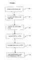
- FIG. 1is a flow chart generally illustrating the process of forming a gate stack in accordance with a preferred embodiment
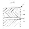
- FIG. 2illustrates a gate stack in accordance with a preferred embodiment
- FIG. 3is a flow chart generally illustrating the process of changing the temperature set point during the deposition process in accordance with a preferred embodiment
- FIG. 4shows a plot of film thickness as a function of measurement site for a preferred SiGe film
- FIG. 5is a reproduction of a scanning electron photomicrograph illustrating a SiGe film deposited using silane and germane;
- FIG. 6is a reproduction of a scanning electron photomicrograph illustrating a cross section of the SiGe film shown in FIG. 5;
- FIG. 7is a reproduction of a scanning electron photomicrograph showing a SiGe film deposited using trisilane and germane;
- FIG. 8is a reproduction of a scanning electron photomicrograph showing a cross section of the SiGe film shown in FIG. 7;
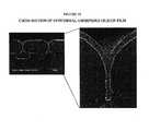
- FIG. 9is a reproduction of a transmission electron photomicrograph showing a cross section of a preferred SiN film
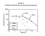
- FIG. 10shows an Arrhenius plot obtained under the conditions described below for silane, disilane, and trisilane
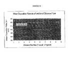
- FIG. 11shows a plot illustrating film deposition rate on an oxide substrate as a function of trisilane (SilcoreTM) flow rate at 600° C., 40 Torr;
- FIG. 12shows a plot illustrating film thickness as a function of position for various deposition times using trisilane (SilcoreTM) at 650° C., 40 Torr;
- FIG. 13shows a plot of deposition rate as a function of diborane flow for deposition using trisilane
- FIG. 14shows a RBS BRD spectrum for an amorphous silicon film deposited using trisilane at 600° C., 40 Torr;
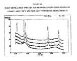
- FIG. 15shows a series of X-ray diffraction patterns obtained for films deposited using trisilane at 600° C., 650° C., 700° C. and 750° C. (bottom to top, respectively);
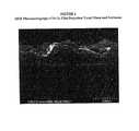
- FIG. 16is a reproduction of a transmission electron photomicrograph of a cross-sectioned polycrystalline silicon film
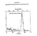
- FIG. 17shows a selected area diffraction pattern for a polycrystalline silicon film
- FIG. 18is a reproduction of a scanning electron photomicrograph of a cross-sectioned conformal amorphous silicon film
- FIG. 19shows a RBS spectrum for a silicon nitride film
- FIG. 20shows a RBS ERD spectrum for a silicon nitride film.
- Dynamic temperature variationsdue to limitations in heating and temperature control systems, play a significant role in the non-uniformity of film deposition on substrate surfaces by CVD. It is generally desirable for the deposited film to be as uniform as possible in both thickness and elemental composition, but existing processes tend to produce films that are non-uniform to varying degrees. Such non-uniformities often result from temperature variations across the surface of the substrate because the surface temperature of the substrate influences the deposition rate and the composition of the resulting film. Imperfect control over other process parameters, including gas flow rates and total pressure, are also believed to contribute to non-uniformities in film physical properties.
- Uniformityis often sought by empirically tuning the deposition conditions e.g., gas flow rate, rotation speed of substrate, power distribution to heating elements, etc., to achieve an overall uniform thickness for the desired film. This is done by first depositing a large number of films on different substrates, each under a different pre-selected set of deposition conditions. The thickness variations within each film are then measured and the results analyzed to identify conditions that would eliminate the thickness variations. The inventors have realized, however, that this empirical process does not necessarily achieve uniform temperature distributions throughout the process; rather, the process effectively time-averages the thickness variations produced by the temperature variations for a specific reaction temperature ‘set-point’.
- the deposition conditionse.g., gas flow rate, rotation speed of substrate, power distribution to heating elements, etc.
- compositional homogeneityor at least control
- compositional homogeneityor at least control
- these dopantsinfluences the electronic properties of the film.
- Non-uniform temperaturescan result in non-uniform incorporation of dopants into the film.
- other non-uniformities in compositioncan result.
- the preferred embodimentsprovide processes for solving this problem, each of which may be used individually or, preferably, together.
- One processinvolves the use of chemical precursors that allow for film deposition to be conducted substantially within a mass transport limited growth regime, relative to conventional precursors at the same temperature.
- the mass transport limited regimeis a temperature range in which film deposition rates are independent of temperature. Deposition rates that are substantially within this temperature range are relatively unaffected by small temperature variations across the surface of the substrate, so long as those variations result in temperatures that remain at or near the mass transport limited regime.
- Thisallows for the production of films that are much more uniform, e.g., exhibit higher compositional uniformity and/or thickness uniformity, than films deposited at the same temperature using conventional chemical precursors. This is because conventional precursors require much higher temperatures in order for deposition to be in the mass transport limited regime.
- the temperature range for the mass transport limited regimecan be determined for a given precursor and set of reaction conditions, and illustrated in an Arrhenius plot.
- the transition point from temperature-dependent deposition rates to temperature-independent deposition ratesis much lower than the transition point for silane or disilane, as illustrated in the Arrhenius plot shown in FIG. 10 .
- the lower region of the plot up to the transitionhas a significant upward linear slope, indicating that deposition of trisilane within this temperature range is a strong function of temperature and therefore not within the mass transport limited regime.
- FIG. 10The lower region of the plot up to the transition has a significant upward linear slope, indicating that deposition of trisilane within this temperature range is a strong function of temperature and therefore not within the mass transport limited regime.
- FIG. 10shows that trisilane deposition is not mass transport limited (i.e., is within the kinetic regime) at temperatures less than about 525° C., under the conditions used (25 sccm flow rate, 40 Torr pressure).
- the region of the plot above the transition pointis substantially flat, indicating that deposition of trisilane within this temperature range is independent of temperature and therefore within the mass transport limited regime.
- FIG. 10shows that trisilane deposition is clearly mass transport limited at temperatures of about 620° C. or greater. It will be understood that the transition occurs over a range of temperatures in which the declining slope of the Arrhenius plot indicates that the deposition of trisilane within this temperature range is substantially independent of temperature, near the mass transport limited regime. For example, FIG.
- trisilane depositionis substantially mass transport limited at temperatures of about 525° C. or greater. It will be understood that the transition point may increase somewhat at higher flow rates, and decrease somewhat at lower flow rates. For example, it has been determined experimentally that the transition point from temperature-dependent deposition to substantially mass transport limited deposition shifts to higher temperatures when the trisilane flow rate is increased. Accordingly, the use of trisilane enables substantially mass transport limited deposition at temperatures that are desirable for other reasons in contemporary fabrication (e.g., conservation of thermal budgets for maintaining crystal properties, controlling dopant profiles, etc.).
- Si- and germanium-containing chemical precursorscan be suitably used in the film deposition processes disclosed herein to provide Si-containing films, Ge-containing films and alloy films that contain both Si and Ge, e.g., silicon germanium (SiGe, without implying stoichiometry) films. These chemical precursors may also be used in conjunction with carbon sources to provide alloy films, e.g., SiGeC (without implying stoichiometry) alloy thin films.
- Particular examplesinclude disilane (H 3 SiSiH 3 ), trisilane (H 3 SiSiH 2 SiH 3 ), and tetrasilane (H 3 SiSiH 2 SiH 2 SiH 3 ).
- Trisilanealso represented by Si 3 H 8
- Si 3 H 8is most preferred for achieving a balance of volatility and reactivity.
- Particular examplesinclude digermane (H 3 GeGeH 3 ), trigermane (H 3 GeGeH 2 GeH 3 ) and tetragermane (H 3 GeGeH 2 GeH 2 GeH 3 ).
- the chemical precursorsare used in conjunction with a source of carbon.
- Additional preferred carbon sourcesinclude hydrocarbons such as methane, ethane, propane, butanes, etc.; carbon monoxide, carbon dioxide and HCN. These chemical precursors and carbon sources may be purchased from commercial sources or synthesized by methods known to those skilled in the art.
- Si-containing filmssuch as SiC, SiNC and SiOC (none of which short forms imply a particular stoichiometry) have a variety of uses in the semiconductor manufacturing industry, e.g., as etch stop layers, hard masks, and passivation layers.
- the filmsare preferably deposited at a temperature that is substantially within the mass transport limited regime for the particular chemical precursor that is used.
- the mass transport limited regimecan be determined from an Arrhenius plot empirically-derived from deposition data at various temperatures. The Arrhenius plot for the most preferred silicon precursor, trisilane, for a particular set of conditions is appended as FIG. 10, discussed above.
- deposition using the first processpreferably involves proper selection of other deposition parameters, particularly gas flow rate.
- gas flow rateProper selection of gas flow rate, in combination with deposition substantially within the mass transport limited regime, has been found to yield films at much higher deposition rates compared to silane, while maintaining a high degree of uniformity.
- film uniformitydepends primarily on the temperature controller set points and, to a much lesser extent, the gas flow rate controller set points.
- the resulting filmis preferably more uniform than a comparable film.
- a “comparable” filmis made in a manner that is substantially identical in all meaningful aspects to the inventive film in question, except that silane is used in place of a higher-order silane and/or germane is used in place of a higher-order germane, and the deposition process for each film is individually tuned to take into account the aforementioned differences in sensitivity to temperature and gas flow controller set points. More particularly, when comparing the results of different layers, thickness uniformity is to be measured by the following standard: a randomly selected diameter across a wafer is employed and 49 points along that diameter are measured for deposited layer thickness.
- the film thicknessis measured at the thinnest part of the cross sectioned film and at the thickest part, and the range in thickness measurements (e.g., ⁇ 6 ⁇ ) between these two points is then divided by the sum of the two measurements.
- This non-uniformityis expressed as a percentage herein.
- the methods employing the precursors described hereinhave been found to result in extraordinarily high deposition rates and yet, surprisingly, obtain exceptionally high uniformity and smoothness.
- a preferred polycrystalline silicon filmis made using trisilane and has greater uniformity at greater deposition rates than a comparable film made from a process separately optimized using silane in place of said trisilane at the same temperature.
- the inventorshave separately experimented with and found amorphous silicon ( ⁇ -Si) layers and epitaxial silicon (epi-Si) layers formed with trisilane to exhibit better uniformity as compared with silane-deposited layers. See FIGS. 15-18 and corresponding text hereinbelow.
- a preferred SiGe filmis made using a higher order germane and has greater uniformity than a comparable film made using germane in place of said higher-order germane.
- higher deposition rates at a lower reaction temperatureare also attainable using the silicon and germanium sources disclosed.
- FIG. 11shows that deposition rate is a linear function of the trisilane (referred to as “SilcoreTM” in some of the figures) flow rate at a deposition temperature of 600° C. and a pressure of 40 Torr.
- This linearityis a further indication that trisilane deposition is substantially or nearly mass transport limited under these conditions and further indicates very low nucleation times over oxide.
- FIG. 12is a plot of film thickness as a function of measurement site for films deposited using trisilane under identical conditions (650° C., 40 torr), except that the deposition time was varied over a range from 90 seconds to 15 seconds as indicated.
- FIG. 12shows that, at a fixed trisilane flow rate, exceptional film uniformity is obtained for a wide range of deposition times, indicating that the results arc not merely time-averaged but result from the nature of the precursor and selected conditions, and further that emissivity (or other thickness-dependent temperature control) effects do not alter the uniformity, since the layers remain uniform regardless of thickness.
- FIG. 13is a plot of the deposition rates obtained using trisilane and diborane (a dopant precursor) at a deposition temperature of 600° C. and a pressure of 40 Torr, over a range of diborane flow rates (zero to 180 sccm).
- FIG. 13shows that deposition rates using trisilane are relatively insensitive to the flow rate of the dopant precursor.
- the preferred temperature rangetends to depend on the particular chemical precursor, with lower temperatures being more appropriate as the thermal stability decreases. For higher-order silanes and higher order germanes, lower temperatures are preferred as chain-length increases. Thus, the preferred temperature range for disilane deposition tends to be higher than for trisilane, which in turn tends to be higher than for tetrasilane, etc. A similar trend holds for the germane series.
- a preferred temperature for depositing trisilaneis higher than about 350° C., preferably higher than about 450° C. in order to minimize hydrogen content in the resulting film.
- temperaturesare maintained higher than about 525° C., even more preferably higher than about 550° C., most preferably higher than about 600° C.
- the processmay be carried out at a temperature above 700° C., but a temperature of about 700° C. or less is preferred.
- Preferred temperaturesare thus in the range of 450° C. to about 700° C., more preferably in the range from about 525° C. to about 650° C.
- the most preferred temperature rangemay be found through routine experimentation, following the guidelines provided herein. It will be understood that the listed temperatures are preferred for thermal CVD. Lower temperatures will be appropriate for plasma assisted deposition processes, depending upon the level of hydrogen incorporation that is acceptable for the application.
- Deposition temperaturecan also depend partly upon the desired crystallinity in the layer being deposited.
- predominantly crystalline siliconcan be deposited in the range of about 620° C. to 800° C., which is clearly within the mass transport limited regime, as discussed above.
- polysilicon depositionis conducted between 650° C. and 750° C.
- Lower temperaturescan be used for amorphous silicon deposition, but preferably temperatures are selected to remain at least substantially mass transport limited (i.e., preferably at higher than 525° C. for the preferred conditions).
- Epitaxial siliconis largely dependent upon the purity of the surface upon which deposition is to take place.
- an extremely clean single-crystal surfacesuch as the upper surface of a previously-deposited epitaxial layer or the upper surface of a single crystal wafer, enables epitaxial deposition at a large range of temperatures, depending upon flow rates, pressure, etc.
- epitaxial deposition upon a suitable surfacecan take place between 500° C. and 1160° C. It is preferred to employ the lower temperature ranges, such as from about 500° C. to about 750° C., for reasons of consideration of thermal budgets. See FIGS. 15-18 and corresponding text hereinbelow.
- depositionis carried out using a chemical precursor e.g., higher-order silane and/or higher-order germane, at a temperature that is effective to achieve higher deposition rates and/or more uniform films, as compared to comparable films made using silane and/or germane.
- a chemical precursore.g., higher-order silane and/or higher-order germane
- Deposition of these chemical precursorsmay be suitably conducted according to the various vapor deposition methods known to those skilled in the art, but the greatest benefits are obtained when deposition is conducted according to the improved chemical vapor deposition (CVD) process techniques taught herein.
- the disclosed processesmay be suitably practiced by employing CVD, including plasma-enhanced chemical vapor deposition (PECVD) or thermal CVD, utilizing a feed gas comprised of a Si- and/or Ge-containing chemical precursor to deposit a Si- and/or Ge-containing film onto a substrate contained within the CVD chamber.
- the gasis comprised of trisilane and a Si-containing film is deposited.
- the gasis comprised of a higher-order silane and a higher-order germane, and a SiGe film is deposited.
- a suitable manifoldmay be used to supply feed gas(es) to the CVD chamber.
- Experimental results described hereinwere conducted in a CVD chamber with horizontal gas flow, and preferably the chamber is a single-wafer, horizontal gas flow reactor, preferably radiatively heated.
- Suitable reactors of this typeare commercially available, and preferred models include the EpsilonTM series of single wafer epitaxial reactors commercially available from ASM America, Inc. of Phoenix, Ariz. While the processes described herein can also be employed in alternative reactors, such as a showerhead arrangement, benefits in increased uniformity and deposition rates have been found particularly effective in the horizontal, single-pass, laminar gas flow arrangement of the EpsilonTM chambers.
- the chemical precursorsare preferably supplied to the CVD chamber in the form of a feed gas or as components of a feed gas, at the temperatures and pressures used for deposition.
- the total pressure in the CVD chamberis preferably in the range of about 0.001 Torr to about 700 Torr, more preferably in the range of about 0.1 Torr to about 200 Torr, most preferably in the range of about 1 Torr to about 60 Torr.
- the partial pressure of each Si- and/or Ge-containing chemical precursoris preferably in the range of about 1 ⁇ 10 ⁇ 6 % to about 100% of the total pressure, more preferably about 1 ⁇ 10 ⁇ 4 % to about 100%, same basis.
- each carbon sourceif any, is preferably in the range from 0% to about 1% of the total pressure, more preferably about 1 ⁇ 10 ⁇ 6 % to about 0.1%, same basis. If used, the partial pressure of the carbon source is preferably effective to provide the resulting Si-containing and/or Ge-containing film with a carbon content of about 20% or less (10% or less for single crystal materials), even more preferably about 10% or less (5% or less for single crystal materials), where the percentages are by weight based on total film weight.
- the feed gascan also include gases other than chemical precursor(s) and carbon sources, such as inert carrier gases.
- exemplary carrier gasesinclude helium, argon, krypton and neon.
- Hydrogenis most preferred as a carrier gas for the processes described herein, particularly for single crystal materials. Nitrogen can also be employed for polycrystalline and amorphous film deposition. Other compounds can be present in the feed gas as desired.
- the gasis further comprised of one or more compounds selected from the group consisting of silane, disilane, tetrasilane, germane, digermane, trigermane, NF 3 , monosilylmethane, disilylmethane, trisilylmethane, tetrasilylmethane, and a dopant precursor.
- Dopant precursorsinclude diborane, deuterated diborane, phosphine, and arsine.
- SbH 3 and trimethylindiumare preferred sources of antimony and indium, respectively.
- Such dopants and dopant sourcesare useful for the preparation of preferred films such as boron-, phosphorous-, antimony-, indium-, and arsenic-doped silicon, SiGe and SiGeC films, by the methods described herein.
- the dopant concentration in these materialswhen doped, is preferably in the range of from about 1 ⁇ 10 14 to about 1 ⁇ 10 22 atoms/cm 3 .
- Dopantscan be incorporated using very low concentrations of the dopant sources, e.g., as mixtures in hydrogen with concentration ranging from about 1 ppm to about 1%, by weight based on total. These diluted mixtures can then be delivered to the reactor via a mass flow controller with set points ranging from 10 to 200 standard cubic centimeters per minute (sccm), depending on desired dopant concentration and dopant gas concentration.
- the dopant sourceis also preferably further diluted in the carrier gas delivered to the reactor with the silicon/germanium/carbon sources. Since typical flow rates often range from about 20 standard liters per minute (SLM) to about 180 SLM, the concentration of the dopant used in a typical process is typically very small.
- the relative partial pressures of the chemical precursors (and carbon source, if any)can be held relatively constant over the course of depositing the Si-containing and/or Ge-containing film, or can be varied to produce a graded film that has differing amounts of Si and/or Ge as a function of depth within the thickness of the film.
- the filmhas a thickness in the range of about 10 ⁇ to about 5,000 ⁇ .
- the elemental composition of the filmmay vary in a stepwise and/or continuous fashion. Film thickness may be varied according to the intended application as known in the art, by varying the deposition time and/or gas flow rates. Whether constant or graded, compound and doped films deposited by the methods described herein have relatively constant composition across a plane at any particular given depth. The “plane” in this sense may undulate if the film is deposited over a patterned substrate.
- Deposition of the films described hereinis preferably conducted at a rate of about 50 ⁇ per minute or higher, more preferably about 75 ⁇ per minute or higher, most preferably about 100 ⁇ per minute or higher.
- the resulting Si-containing filmis preferably selected from the group consisting of a SiGe film, a SiGeC film, a silicon nitride film (SiN, without implying stoichiometry), a silicon oxide film (SiO, without implying stoichiometry), a silicon oxynitride film (SiON, without implying stoichiometry), a boron-doped film, an arsenic-doped film, a phosphorous-doped film, and a film having a dielectric constant of about 2.2 or lower.
- the Si-containing filmcan be amorphous, polycrystalline or epitaxial. Trisilane has been shown to be particularly advantageous for improving deposition rates and uniformity of epitaxial silicon layers.
- the preferred embodimentsalso provide another process for solving the uniformity problems discussed above. Examples of this process are given in FIG. 3 and Example 39, and the process is described more generally here.
- Through-thickness compositional non-uniformities in deposited filmsare believed to result from, inter alia, dynamic (as opposed to static) variations in substrate surface temperature.
- CVD chambersare generally equipped with a temperature controller that is configured to allow programming with a set of temperature control conditions that are kept constant throughout the deposition of a particular layer. This set point temperature is generally selected at the beginning of the process and maintained until the layer is completed.
- the thickness problemwas approached in the past by empirically tuning the deposition conditions e.g., gas flow rate, rotation speed of substrate, power distribution to heating elements, etc., to effectively time-average the thickness effects of the temperature variations.
- a layer-by-layer approachcan be used to produce films having greater uniformity.
- a set of empirically-determined temperature set points T 1 , T 2 , T 3 , etc.can be determined on a layer-by-layer basis.
- a single film, having a single function at a particular point in an integrated circuit,is broken down into several layers during the empirical determination and optimal set points are determined for each layer. Accordingly, temperature control variations caused by the growing thickness of the film can be compensated by use of separately optimized set points during the deposition process.
- Such an empirical determinationcan be conducted by first depositing a first layer on each of a number of separate workpieces using various temperature set points, then measuring the thickness and compositional variation of the first layer on each workpiece to identify which set point resulted in the most uniform layer.
- the target thickness of the layermay vary as desired, e.g., from about 50 ⁇ to about 1,000 ⁇ , preferably about 100 ⁇ to about 700 ⁇ , depending on the level of uniformity required for the particular application.
- a first layeris then prepared on several more workpieces at the identified set point T 1 to serve as substrates for the empirical determination of the second set point T 2 .
- a second layeris deposited onto the first film of each of these workpieces using various temperature set points, then the thickness and compositional variation of each layer is measured to identify which second set point resulted in the most uniform second layer.
- the target thickness of the second layermay vary as desired, e.g., from about 50 ⁇ to about 1,000 ⁇ , preferably about 100 ⁇ to about 700 ⁇ , depending on the level of uniformity required for the particular application.
- the processcan then be halted, if the optimized first and second layers form a multi-layer film having the desired thickness and degree of uniformity.
- the processcan be continued by, e.g., preparing a batch of workpieces having two layers deposited at the first two identified set points T 1 and T 2 , depositing a third layer onto the second layer of each workpiece using various temperature set points, measuring the thickness and compositional variation of each layer to identify which third set point T 3 resulted in the most uniform third layer, etc.
- Temperature set pointis used herein as an example of a temperature control variable that is normally kept constant during a deposition process, but that can be varied during deposition by the empirical process taught above. This empirical process can also be applied to other temperature control variables that are normally kept constant during a single film deposition process, such as temperature offsets for a PID controller or PD coefficient(s).
- Process variablessuch as gas flow rate, gas flow distribution, partial pressure and gas composition are preferably varied in processes similar to that described above for identifying the temperature set point, or during the same experiments, in order to identify the desired deposition conditions for each layer.
- experimental design methodsare used to determine the effect of the various process variables and combinations thereof on uniformity and/or deposition rate. Experimental design methods per se are well-known, see e.g., Douglas C. Montgomery, “Design and Analysis of Experiments,” 2 nd Ed., John Wiley and Sons, 1984.
- the processis preferably automated by computer control to ensure batch-to batch or wafer-to-wafer consistency.
- the process improvementsresult from in-situ, stepwise or dynamic adjustments to the process variables mentioned above.
- This empirical method of tuning process variables to individually improve the properties of the layershas been found to improve the properties of the overall single structural or functional film (comprising multiple layers from a process standpoint) regardless of any theory expressed herein. Therefore, the functioning of this embodiment does not depend on the correctness or incorrectness of any theory.
- the preferred embodimentmay be practiced using a CVD chamber that is equipped with a temperature controller configured to allow programming with multiple temperature set points for a single recipe.
- the processis preferably conducted by entering a temperature set point T 1 into a temperature controller and introducing a first gas comprised of X 1 % of a first Si-containing chemical precursor to the CVD chamber; where X 1 is in the range of about 0 to about 100.
- a first Si-containing layeris then deposited onto a substrate contained within the chamber.
- the processis preferably continued by entering a temperature set point T 2 into the temperature controller, introducing a second gas comprised of X 2 % of a second Si-containing chemical precursor to the CVD chamber, and depositing a second Si-containing layer onto the first Si-containing layer, thereby forming a multi-layer Si-containing film.
- the second Si-containing chemical precursormay be chemically identical to the first Si-containing chemical precursor or may be different, as discussed below and illustrated by FIG. 3 and Example 39.
- the processcan be continued further by, e.g., entering a temperature set point T 3 into the temperature controller, introducing a third gas comprised of X 3 % of a third Si-containing chemical precursor to the CVD chamber, and depositing a third Si-containing layer onto the second Si-containing layer, and so on, producing as many layers as desired.
- Preferred Si-containing chemical precursorsinclude higher order silanes as described elsewhere herein, as well as conventional chemical precursors such as silane.
- Preferably at least one of the first Si-containing chemical precursor and the second Si-containing chemical precursoris selected from the group consisting of silane, disilane and trisilane.
- At least one of the first gas, second gas and third gasis preferably comprised of a compound selected from the group consisting of germane, digermane, trigermane, NF 3 , monosilylmethane, disilylmethane, trisilylmethane, tetrasilylmethane, and a dopant precursor, as described elsewhere herein.
- the amount of each Si-containing chemical precursor X n , for X 1 %, X 2 %, X 3 %, X 4 %, etc., in the gasis independently in the range of about 1 ⁇ 10 ⁇ 6 % to about 100%, preferably about 1 ⁇ 10 ⁇ 4 % to about 100%, by volume based on total volume, at any particular stage of the deposition process.
- the substratepreferably has a temperature of about 350° C. or higher, more preferably in the range of 450° C. to about 700° C.
- the CVD chamberis preferably a single-wafer, horizontal gas flow reactor.
- the resulting multiple layer Si-containing filmis preferably selected from the group consisting of a microdot, a SiGe film, a SiGeC film, a SiN film, a silicon-oxygen film, a silicon-oxygen-nitrogen film, a boron-doped film, an arsenic-doped film, a phosphorous-doped film, and a film having a dielectric constant of about 2.2 or lower.
- the processes of the preferred embodimentsmay be practiced by depositing the multiple layers of the film in a stepwise or continuous fashion.
- process variablessuch as flow rate, partial pressure and gas composition can also be adjusted as desired to produce films having various compositions.
- the deposited filmmay have a homogenous or uniform composition as discussed above, or may vary in composition step-wise or continuously.
- the identity of the Si-containing chemical precursorcan be altered during the pause, and/or the amount in the gas X 1 %, X 2 %, X 3 %, X 4 %, etc. can be varied.
- the processinvolves the growth of a graded germanium concentration layer by noncontinuous or step-wise changes in germanium concentration, preferably achieved by preparing a superlattice with discontinuous periodicity by depositing layers of selected germanium concentration on top of each other.
- Example 39in conjunction with Example 43 below, illustrates this embodiment.
- the overall “film” of this embodimentconstitutes a single structural film from the point of view of its function in an integrated circuit, and will typically have a similar composition throughout its thickness. Similar composition, for defining a single film formed by the stepwise deposition process described above, thus encompasses graded films wherein the same constituents have different concentrations at different points through the thickness of the film.
- Deposition ratesmay be determined by measuring the average thickness of the film as a function of time and can be expressed in units of angstroms per minute ( ⁇ /min.). Preferred deposition rates are about 20 ⁇ /min. or greater, more preferably about 50 ⁇ /min. or greater, most preferably 100 ⁇ /min. or greater. Suitable methods for measuring film thickness include multiple-point ellipsometric methods. Instruments for measuring film thickness are well known and commercially available and preferred instruments include the NanoSpec® series of instruments from Nanometrics, Inc., Sunnyvale, Calif.
- uniformityis used to refer to both thickness uniformity and compositional uniformity.
- Film thickness uniformityis preferably determined by making multiple-point thickness measurements, determining the mean thickness, and determining the average amount that the multiple measurements differ from the mean. To enable comparisons, the result can be expressed as percent non-uniformity. Preferably, the percent non-uniformity is about 10% or less, more preferably about 5% or less, most preferably about 2% or less.
- Compositional uniformitymay be determined using electrical measurements (i.e.
- compositional uniformityis measured using SIMS across a circular wafer substrate onto which the Si-containing has been deposited.
- SIMS measurementsare made at three locations: one at the center of the wafer, one at a point midway between the center and the edge (“r/2”), and one at a point 3 millimeters from the edge (“3 mm edge exclusion”).
- the amount of that element at each locationis then determined from the SIMS data, and the resulting value expressed in atomic % based on total. The three values are then averaged, and the standard deviation determined.
- the compositional non-uniformity for the Si-containing filmis preferably about 25% or less, more preferably about 20% or less, even more preferably about 15% or less, most preferably about 10% or less.
- Ge content in SiGe filmswill typically represent greater than about 1 atomic % of such films, such that the above preferences apply to SiGe films.
- the amount of elementis in the range of 0.001 atomic percent up to 1 atomic %, the compositional non-uniformity for the Si-containing film is preferably about 100% or less, more preferably about 75% or less, even more preferably about 50% or less, most preferably about 25% or less.
- the compositional non-uniformity for the Si-containing filmis preferably in the range of about 400% or less, more preferably about 300% or less, even more preferably about 200% or less, most preferably about 100% or less.
- Ge content in graded SiGe films, for example,may vary over a broad range, and thus more than one of the above ranges may apply depending on the profile.
- FIG. 14is a Rutherford Backscattering spectrum (elastic recoil detection, ERD) of an amorphous silicon film deposited using trisilane at a deposition rate of 1306 ⁇ per minute and a pressure of 40 Torr, at a deposition temperature of 600° C.
- the solid linesare the raw data from the film and the dashed line is a model generated from the data simulation software RUMPTM for an assumed residual hydrogen concentration of 0.5 at. %.
- the raw dataindicate slight surface contamination, possibly due to absorbed hydrocarbons and/or moisture, but the spectrum indicates that the residual hydrogen concentration within the film is below detection limits, corresponding to a hydrogen concentration of less than 0.2 atomic %.
- FIG. 15shows X-ray diffraction spectra for a series of silicon films deposited using trisilane at deposition temperatures of 600° C., 650° C., 700° C. and 750° C. (bottom to top of FIG. 15, respectively).
- the X-ray diffraction patternsshow that the film deposited at 600° C. was amorphous, the film deposited at 650° C. was partially crystalline, and that the films deposited at 700° C. and 750° C. were increasingly more crystalline.
- FIG. 16shows a reproduction of a transmission electron photomicrograph of a cross section of the film deposited at 750° C.
- FIG. 18shows a reproduction of a scanning electron photomicrograph of a cross section of an amorphous silicon film deposited using trisilane at 600° C. and 40 Torr. The film was deposited onto a curved substrate and shows excellent conformality even into deep, narrow seams.
- higher-order silanesmay also be employed for the CVD synthesis, preferably low temperature, low pressure CVD, of silicon nitride (SiN) materials with compositions ranging from almost pure silicon to Si 3 N 4 .
- Preferred nitrogen sourcesinclude chemical precursors such as (H 3 Si) 3 N (trisilylamine), ammonia, atomic nitrogen, and NF 3 .
- Atomic nitrogenis preferably generated using a remote microwave radical generator.
- the relative amounts of nitrogen source and higher-order silane introduced to the CVD chamberare preferably selected to provide the resulting SiN film with a greater degree of uniformity than a comparable film made using silane in place of the higher-order silane.
- atomic nitrogenis introduced continuously, and trisilane is introduced either continuously or in pulses, preferably in one or more pulses. It has been found that greater film uniformity can be obtained by introducing the higher-order silane in pulses, and that extremely thin, highly uniform SiN films can be obtained by intermittent CVD, as demonstrated in the Examples below.
- Preferred SiN films prepared in accordance with this embodimenthave a thickness in the range of about 10 ⁇ to about 300 ⁇ , more preferably about 15 ⁇ to about 150 ⁇ .
- higher-order silanesmay also be employed for the CVD synthesis, preferably low temperature, low pressure CVD, of silicon oxide materials and silicon oxynitride materials.
- the oxygen source(s)can include ozone, oxygen, water, nitric oxide, nitrous oxide, hydrogen peroxide and the like.
- the nitrogen sources for the introduction of nitrogen into these materialsinclude trisilylamine, atomic nitrogen, ammonia, and NF 3 (as described above). Such oxygen and nitrogen sources can be employed continuously or in discrete steps or in a method involving a combination of these processes.
- depositionis conducted in at least the nearly mass transport limited regime, as discussed above.
- Deposition using trisilylamine and trisilaneis preferably conducted in the range of about 350° C. to about 750° C., more preferably about 400° C. to about 700° C., most preferably about 450° C. to about 650° C.
- Deposition using NF 3 and trisilaneis preferably conducted in the range of about 300° C. to about 750° C.; more preferably about 350° C. to about 700° C., most preferably about 400° C. to about 650° C.
- a preferred embodimentprovides films useful in the microelectronic industry for various applications.
- a preferred Si-containing filmhas a thickness non-uniformity of less than about 2% and a compositional non-uniformity as described above, with respect to different proportions of elements in the film.
- Films such as described hereinare useful in various applications, e.g., as a transistor gate electrode.
- the layers described hereinare particularly useful for forming critical device layers in integrated circuits, such as gate layers in integrated transistors.
- Other examplesinclude semiconductor layers in heterojunction bipolar transistors (HBT's). Processes for making such integrated circuits from such films are known to those skilled in the art.
- HBT'sheterojunction bipolar transistors
- FIG. 1is a flow diagram showing a preferred process flow in which deposition processes described herein can be employed.
- a gate dielectricis formed 100 over a semiconductor substrate.
- the gate dielectricis cleaned 110 , if necessary, and a silicon-containing layer is deposited 120 , as described herein, preferably including flowing trisilane.
- An optional further metal layercan also be deposited 130 over the Si-containing, if desired for improved lateral signal transmission.
- These multiple layersare then photolithographically patterned 140 , and fabrication continues 150 .
- FIG. 2illustrates a gate stack 200 formed by the process of FIG. 1.
- a gate dielectric 210is formed over a semiconductor substrate 220 .
- An electrically doped Si-containing film 230is formed over the gate dielectric 210 and an optional metal layer 240 is positioned over the Si-containing film 230 to form the gate stack 200 .
- the stack 200is then patterned to form gate electrodes (not shown in FIG. 2) and the fabrication of the integrated circuit is continued.
- the gate dielectric 210comprises at least one high k material, with a dielectric constant greater than 5 and more preferably greater than 10.
- Exemplary materialscomprise aluminum oxide, hafnium oxide and zirconium oxide, preferably formed by atomic layer deposition (ALD) for high quality, pinhole free layers.
- ALDatomic layer deposition
- epitaxial Si-containing layersare deposited, flowing trisilane, over single-crystal substrates.
- Silicon layers and heteroepitaxial SiGe, SiC and SiGeC layerscan be deposited by processes described herein.
- This apparatuscomprises a CVD chamber, a vessel containing trisilane, a feed line operatively connecting the vessel to the CVD chamber to allow passage of the trisilane from the vessel to the CVD chamber, and a temperature controller operatively disposed about said vessel and maintained at a temperature in the range of about 10° C. to about 70° C., preferably 15° C. to about 52° C., to thereby control the vaporization rate of the trisilane.
- suitable temperature controllersinclude thermoelectric controllers and/or liquid-filled jackets.
- the CVD chamberis a single-wafer, horizontal gas flow reactor.
- the apparatusis also comprised of a manifold operatively connected to the feed line to control the passage of the trisilane from the vessel to the chemical vapor deposition chamber.
- a heat sourceis operatively disposed about the feed line and the gas lines are heated to about 35° C. to about 70° C., more preferably between about 40° C. and 52° C., to prevent condensation at high gas flow rates.
- trisilaneis introduced by way of a bubbler used with a carrier gas to entrain trisilane vapor, more preferably a temperature-controlled bubbler, most preferably a temperature-controlled bubbler in combination with heated gas lines to deliver trisilane.
- the following exampleswere conducted using an ASM Epsilon 2000TM horizontal flow epitaxial reactor system, configured with a Bernoulli wand wafer transfer system, purge-only load locks, a non-slide concave susceptor, a ‘square’ pre-heat ring, adjustable spot lamps and independently tunable gas inlet injectors.
- the Si-containing and Ge-containing precursorswere supplied to the chamber in a feed gas that also contained hydrogen and a diborane dopant.
- Si-containing filmswere deposited using trisilane as chemical precursor according to the parameters shown in Table 1.
- the deposition temperaturewas 700° C., well within the mass transport limited regime for trisilane.
- the resulting filmswere not uniform and instead had a concave deposition profile (thin in middle and thicker at edges) because the flow rate was inadequate (under these particular deposition conditions) to provide a uniform film.
- Si-containing amorphous filmswere deposited using trisilane and silane as chemical precursors and diborane as a dopant according to the parameters shown in Table 1.
- About 120 sccm of 1% B 2 H 6 in H 2was diluted in 2 slm H 2 and 120 sccm of this mixture was introduced into the reactor where it was mixed with 20 slm H 2 and trisilane or silane at the flow rate shown in Table 2.
- Si-containing filmswere deposited using trisilane and silane as chemical precursors, according to the parameters shown in Table 3. Deposition times were adjusted so that the films each had an average thickness of about 500 ⁇ . Deposition rates were determined by measuring average film thickness using a Nanometrics ellipsometer and then dividing this number by the deposition time. Film non-uniformity was determined from a 49-point thickness map of the film thickness. The results show that a much more uniform film was obtained at a much higher deposition rate by using trisilane at the indicated temperature in place of silane. This is true at 550° C., but dramatically more so at 600° C.
- Examples 1-19are repeated except that SiGe films are obtained by using a mixture of 80% trisilane and 20% digermane in place of trisilane alone, and by using a mixture of 80% silane and 20% germane in place of silane. Higher deposition rates were observed than with the use of trisilane or silane alone.
- a SiGe filmis prepared by superlattice growth with discontinuous periodicity as follows, with reference to the flow chart shown in FIG. 3.
- a Si ⁇ 100> substrateis prepared 300 by performing an ex-situ hydrogen-fluoride (HF) last clean to remove the native oxide layer, followed by introducing the substrate into a reactor chamber under a high flow of ultra-pure hydrogen gas.
- the waferis rotated at 60 rpm while the wafer is heated to about 900° C. under a high flow of hydrogen gas (to remove any contaminants from the substrate surface).
- the waferis cooled and allowed to stabilize at 700° C. and an arsenic-doped silicon buffer layer about 300 ⁇ thick is grown using trisilane and trisilylarsine under mass transport limited conditions.
- the wafer temperatureis adjusted 310 by cooling under hydrogen flow to 600° C.
- the first period of SiGe superlatticeis grown 320 using 98% disilane and 2% digermane.
- a second period of SiGe superlatticeis grown 330 using 85% trisilane and 15% digermane.
- the set point temperatureis lowered 340 by 3° C. and the wafer is allowed to stabilize for 30 seconds.
- a third period of SiGe superlatticeis grown 350 using 75% trisilane and 25% digermane.
- the set point temperatureis lowered 350 by 3° C. and the wafer is allowed to stabilize for 30 seconds.
- a fourth period of SiGe superlatticeis grown 370 using 65% trisilane and 35% digermane.
- a fifth period of SiGe superlattice doped with carbon and boronis grown 380 using 85% trisilane, 12% digermane, 2% diborane and 1% disilylmethane.
- the reactoris purged 390 for 30 seconds.
- a sixth period of SiGe superlatticeis grown 400 using 90% trisilane and 10% digermane.
- the temperature set pointis increased 410 to 650° C. and the relative powers of the lamp banks are adjusted slightly to maximize the within-wafer uniformity of the silicon cap layer to be grown 420 .
- the waferis allowed to stabilize for 30 seconds.
- the silicon cap layeris grown using 100% trisilane.
- the waferis removed 430 from the reactor and next wafer is processed.
- a Si-containing film having a mean thickness of 1,038 ⁇was deposited using trisilane and germane as chemical precursors at a deposition temperature of 650° C. and a pressure of 40 torr.
- the set points for gas flow injectorshad been empirically tuned in the usual manner in a series of previous runs.
- the resulting SiGe filmhad a thickness non-uniformity of 0.37% (range of 8 ⁇ ) as measured by a 49 point linear dimension scan with 6 mm edge exclusion.
- FIG. 4is a plot of film thickness as a function of measurement site for this film.
- a Si-containing filmwas deposited onto a SiO 2 substrate (without a nucleation layer) at a temperature of 600° C. using silane and germane as precursors.
- the surface roughness of the resulting SiGe filmwas 226 ⁇ for a 10 micron ⁇ 10 micron scan area.
- Scanning electron microscopy (SEM) of the SiGe filmrevealed pyramidal, faceted grains indicative of an island-type deposition, as demonstrated in the SEM micrographs shown in FIGS. 5 and 6.
- a Si-containing filmwas deposited at 600° C. as described in Example 41, but trisilane and germane was used in place of silane and germane as precursors.
- the surface roughness of the resulting SiGe filmwas 18.4 ⁇ for a 10 micron ⁇ 10 micron scan area.
- SEM of the SiGe filmrevealed a much more uniform surface, as demonstrated in the SEM micrographs shown in FIGS. 7 and 8 (same magnifications and tilt angles as FIGS. 5 and 6, respectively).
- a series of Si-containing filmswere deposited onto a SiO 2 substrate (without a nucleation layer) at a pressure of 40 torr using trisilane and germane.
- the trisilane flow ratewas constant at 77 sccm (hydrogen carrier, bubbler) for the examples of Table 4.
- Germane flow (10% germane, 90% H 2 ) and deposition temperaturewere varied as shown in Table 4.
- Germanium concentration (atomic %) and thickness of the resulting SiGe filmswere determined by RBS, and surface roughness was determined by atomic force microscopy (AFM).
- the results shown in Table 4demonstrate that highly uniform films can be prepared over a range of temperatures and flow rate conditions, particularly over a range of germane concentration.
- FIG. 19is a representative RBS spectrum (2 MeV He ++ ) of a silicon nitride sample deposited using trisilane at 775° C. and 20 Torr.
- An ERD spectrum obtained using Elastic Recoil Detection (ERD)is shown in FIG. 20 .
- ERDElastic Recoil Detection
- a series of Si-containing materialswere deposited onto the native oxide of Si ⁇ 100> substrates using trisilane and atomic nitrogen.
- Atomic nitrogenwas generated remotely using a commercially available 800 watt microwave radical generator (MRG) and was supplied to the CVD chamber.
- Trisilanewas supplied to the CVD chamber along with the atomic nitrogen via a bubbler using a nitrogen carrier gas at a flow rate of 5 slm (10 slm for Example 82), at the deposition temperatures shown in Table 6.
- Trisilanewas introduced to the chamber either continuously (Example 79) or in pulses (Examples 80-82). Pulsed introduction was accomplished by continuously introducing atomic nitrogen, and introducing trisilane in pulses at intervals of about 1 minute and 30 seconds. Each of the trisilane pulses lasted about 6 seconds, under the flow conditions described above.
- Each of the resulting SiN filmshad a stoichiometry in the range of approximately Si 43 N 54-56 H 3-1 .
- Table 6shows the thicknesses, refractive indices and hydrogen levels (atomic %) in the resulting SiN films.
- the SiN film of Example 79was not uniform because it was significantly thicker at the center than the edge, and the measured refractive index varied significantly across the surface of the film (higher at center than edge). Uniformity was improved by using the pulsed processes of Examples 80-82. Uniform films can also be obtained using the continuous process by increasing the flow rate of atomic nitrogen and/or decreasing the flow rate of trisilane.
- a thin, uniform, continuous SiN film having a thickness of about 18 ⁇was deposited at 650° C. at a pressure of 3 torr using remotely generated atomic nitrogen and a single six-second pulse of trisilane, as generally described above for Examples 80-82.
- the filmwas coated with epoxy, cross-sectioned and imaged using transmission electron microscopy (TEM), as shown in the TEM photomicrograph of FIG. 9 .
- TEMtransmission electron microscopy
- a series of epitaxial silicon filmswere deposited onto cleaned Si ⁇ 100> substrates using trisilane at a deposition pressure of 40 Torr and various flow rates, and at the deposition temperatures and deposition rates shown in Table 7.
- High quality epitaxial silicon filmswere produced, as indicated by the ⁇ -min values obtained from Rutherford Backscattering channeling spectra as shown in Table 7.
Landscapes
- Chemical & Material Sciences (AREA)
- Engineering & Computer Science (AREA)
- Physics & Mathematics (AREA)
- Condensed Matter Physics & Semiconductors (AREA)
- General Physics & Mathematics (AREA)
- Manufacturing & Machinery (AREA)
- Computer Hardware Design (AREA)
- Microelectronics & Electronic Packaging (AREA)
- Power Engineering (AREA)
- Materials Engineering (AREA)
- General Chemical & Material Sciences (AREA)
- Chemical Kinetics & Catalysis (AREA)
- Metallurgy (AREA)
- Organic Chemistry (AREA)
- Crystallography & Structural Chemistry (AREA)
- Mechanical Engineering (AREA)
- Inorganic Chemistry (AREA)
- Nanotechnology (AREA)
- Theoretical Computer Science (AREA)
- Mathematical Physics (AREA)
- Composite Materials (AREA)
- Chemical Vapour Deposition (AREA)
- Formation Of Insulating Films (AREA)
- Electrodes Of Semiconductors (AREA)
- Bipolar Transistors (AREA)
- Metal-Oxide And Bipolar Metal-Oxide Semiconductor Integrated Circuits (AREA)
- Insulated Gate Type Field-Effect Transistor (AREA)
- Led Devices (AREA)
- Separation Using Semi-Permeable Membranes (AREA)
- Physical Vapour Deposition (AREA)
- Thin Film Transistor (AREA)
Abstract
Description
This application claims priority to U.S. Provisional Application No. 60/268,337, filed Feb. 12, 2001; U.S. Provisional Application No. 60/279,256, filed Mar. 27, 2001; U.S. Provisional Application No. 60/311,609, filed Aug. 9, 2001; U.S. Provisional Application No. 60/323,649, filed Sep. 19, 2001; U.S. Provisional Application No. 60/332,696, filed Nov. 13, 2001; U.S. Provisional Application No. 60/333,724, filed Nov. 28, 2001; and U.S. Provisional Application No. 60/340,454, filed Dec. 7, 2001; all of which are hereby incorporated by reference in their entireties. This application is related to, and incorporates by reference in their entireties, co-owned and co-pending U.S. patent application Ser. No.: 10/074,149 now U.S. Pat. No. 6,716,759; U.S. patent application Ser. Nos. 10/074,722; 10/074,633; 10/074,564; and 10/074,534, all of which were filed on February 11, 2002.
1. Field of the Invention
This invention relates generally to depositing semiconductor films, such as those containing Si, Ge and/or carbon for integrated circuit fabrication. More particularly, the invention relates to making these materials with greater thickness and compositional uniformity in chemical vapor deposition systems.
2. Description of the Related Art
As the dimensions of microelectronic devices become smaller, the importance of the physical and chemical properties of the materials used in their manufacture becomes more important. This is particularly true for those advanced materials that can be integrated into existing generations of devices using already-proven manufacturing tools. For example, it would be desirable to incorporate epitaxial Si1−xGexand Si1−x−yGexCyalloys into Bipolar and BiCMOS device manufacturing processes. These advanced alloy materials have utility as base layers in heterojunction bipolar transistors (HBT), resistors in BiCMOS devices and as gate electrodes in CMOS devices and various other integrated electronic devices.
Conventional processes for the deposition of single crystal, amorphous and/or polycrystalline silicon, silicon germanium (SiGe) and silicon germanium carbon (SiGeC) alloys arc typically performed using batch thermal processes (either low pressure (LP) or ultra-high vacuum (UHV) conditions) or single wafer processes. Single wafer processes are becoming increasingly significant, but a number of problems remain. For instance, within-wafer and wafer-to-wafer uniformity, deposition rates, and process repeatability remain a concern with conventional single wafer processes, particularly for in situ doped semiconductor films. As wafers continue to increase in size (currently 300 mm wafers are being integrated into fabrication processes), maintaining uniformity is becoming more challenging still.
Japanese Patent Application Disclosure Number S60-43485 discloses the use of trisilane to make amorphous thin films at 300° C., apparently for photovoltaic applications. Japanese Patent Application Disclosure Number H5-62911 discloses the use of trisilane and germane to make thin films at 500° C. or less. Japanese Patent Application Disclosure Number H3-91239, H3-185817, H13-187215 and HO2-155225 each disclose the use of disilane, some also mentioning trisilane.
The art has generally focused on the use of disilane and trisilane for producing amorphous, hydrogenated silicon at relatively low deposition temperatures. However, there remains a need for a process for depositing semiconductor materials such as doped silicon, low-H content amorphous silicon and SiGe onto surfaces, preferably at high deposition rates without sacrificing good uniformity.
The inventors have discovered better ways of making Si-containing and Ge-containing films. Methods are taught for using chemical precursors such as higher-order silanes and/or higher-order germanes in CVD processes to provide improved deposition of Si-containing films, particularly silicon, SiGe or SiGeC alloy thin films useful in the semiconductor industry. These chemical precursors have reduced thermal stability relative to silane, germane and conventional carbon-source molecules.
In accordance with one aspect of the invention, the use of particular precursors allows the deposition process to be conducted closer to, or within, a mass transport limited growth regime, relative to conventional precursors at the same temperature. Within this regime, temperature dependent non-uniformities, such as undesirable elemental concentration gradients and variable film deposition rates, and consequent thickness non-uniformities, can be avoided. Preferred chemical precursors include trisilane and trisilane in combination with digermane. Uniform deposition can be achieved at temperatures lower than those used for conventional chemical precursors, with higher film deposition rates.
In another aspect of the invention, flow rates of the preferred precursors are adjusted as a function of temperature to obtain higher deposition rates with equal or greater uniformity, as compared with deposition using conventional precursors (e.g., silane). The advantages of trisilane over silane have been found particularly applicable to the deposition of silicon-containing layers as active layers in integrated transistors.
In another aspect of this invention, methods are taught for stepwise or dynamically changing process parameters such as temperature, temperature distribution, pressure, reactant flow rate and reactant partial pressure in such a way as to reduce or eliminate such undesirable elemental concentration gradients, thickness non-uniformities and variable film deposition rates. These methods can be used in conjunction with the use of higher order silanes and/or germanes.
These and other aspects of the invention will be readily apparent from the following description and from the appended drawings, which are meant to illustrate and not to limit the invention, and wherein:
FIG. 1 is a flow chart generally illustrating the process of forming a gate stack in accordance with a preferred embodiment;
FIG. 2 illustrates a gate stack in accordance with a preferred embodiment;
FIG. 3 is a flow chart generally illustrating the process of changing the temperature set point during the deposition process in accordance with a preferred embodiment;
FIG. 4 shows a plot of film thickness as a function of measurement site for a preferred SiGe film;
FIG. 5 is a reproduction of a scanning electron photomicrograph illustrating a SiGe film deposited using silane and germane;
FIG. 6 is a reproduction of a scanning electron photomicrograph illustrating a cross section of the SiGe film shown in FIG. 5;
FIG. 7 is a reproduction of a scanning electron photomicrograph showing a SiGe film deposited using trisilane and germane;
FIG. 8 is a reproduction of a scanning electron photomicrograph showing a cross section of the SiGe film shown in FIG. 7;
FIG. 9 is a reproduction of a transmission electron photomicrograph showing a cross section of a preferred SiN film;
FIG. 10 shows an Arrhenius plot obtained under the conditions described below for silane, disilane, and trisilane;
FIG. 11 shows a plot illustrating film deposition rate on an oxide substrate as a function of trisilane (Silcore™) flow rate at 600° C., 40 Torr;
FIG. 12 shows a plot illustrating film thickness as a function of position for various deposition times using trisilane (Silcore™) at 650° C., 40 Torr;
FIG. 13 shows a plot of deposition rate as a function of diborane flow for deposition using trisilane;
FIG. 14 shows a RBS BRD spectrum for an amorphous silicon film deposited using trisilane at 600° C., 40 Torr;
FIG. 15 shows a series of X-ray diffraction patterns obtained for films deposited using trisilane at 600° C., 650° C., 700° C. and 750° C. (bottom to top, respectively);
FIG. 16 is a reproduction of a transmission electron photomicrograph of a cross-sectioned polycrystalline silicon film;
FIG. 17 shows a selected area diffraction pattern for a polycrystalline silicon film;
FIG. 18 is a reproduction of a scanning electron photomicrograph of a cross-sectioned conformal amorphous silicon film;
FIG. 19 shows a RBS spectrum for a silicon nitride film; and
FIG. 20 shows a RBS ERD spectrum for a silicon nitride film.
Dynamic temperature variations, due to limitations in heating and temperature control systems, play a significant role in the non-uniformity of film deposition on substrate surfaces by CVD. It is generally desirable for the deposited film to be as uniform as possible in both thickness and elemental composition, but existing processes tend to produce films that are non-uniform to varying degrees. Such non-uniformities often result from temperature variations across the surface of the substrate because the surface temperature of the substrate influences the deposition rate and the composition of the resulting film. Imperfect control over other process parameters, including gas flow rates and total pressure, are also believed to contribute to non-uniformities in film physical properties.
Uniformity is often sought by empirically tuning the deposition conditions e.g., gas flow rate, rotation speed of substrate, power distribution to heating elements, etc., to achieve an overall uniform thickness for the desired film. This is done by first depositing a large number of films on different substrates, each under a different pre-selected set of deposition conditions. The thickness variations within each film are then measured and the results analyzed to identify conditions that would eliminate the thickness variations. The inventors have realized, however, that this empirical process does not necessarily achieve uniform temperature distributions throughout the process; rather, the process effectively time-averages the thickness variations produced by the temperature variations for a specific reaction temperature ‘set-point’.
Accordingly, this empirical approach does not necessarily produce uniform temperatures across the substrate throughout the deposition process. This, in turn, raises the issue of compositional variation because compositional homogeneity (or at least control) is desired in three dimensions, both across the film surface and through the film thickness. This is because many films contain dopants and the level of these dopants influences the electronic properties of the film. Non-uniform temperatures can result in non-uniform incorporation of dopants into the film. Similarly, other non-uniformities in composition can result.
The preferred embodiments provide processes for solving this problem, each of which may be used individually or, preferably, together. One process involves the use of chemical precursors that allow for film deposition to be conducted substantially within a mass transport limited growth regime, relative to conventional precursors at the same temperature. For a given chemical precursor, the mass transport limited regime is a temperature range in which film deposition rates are independent of temperature. Deposition rates that are substantially within this temperature range are relatively unaffected by small temperature variations across the surface of the substrate, so long as those variations result in temperatures that remain at or near the mass transport limited regime. This allows for the production of films that are much more uniform, e.g., exhibit higher compositional uniformity and/or thickness uniformity, than films deposited at the same temperature using conventional chemical precursors. This is because conventional precursors require much higher temperatures in order for deposition to be in the mass transport limited regime.
As will be appreciated by the skilled artisan, the temperature range for the mass transport limited regime can be determined for a given precursor and set of reaction conditions, and illustrated in an Arrhenius plot. For the chemical precursor trisilane, the transition point from temperature-dependent deposition rates to temperature-independent deposition rates is much lower than the transition point for silane or disilane, as illustrated in the Arrhenius plot shown in FIG.10. The lower region of the plot up to the transition has a significant upward linear slope, indicating that deposition of trisilane within this temperature range is a strong function of temperature and therefore not within the mass transport limited regime. For example, FIG. 10 shows that trisilane deposition is not mass transport limited (i.e., is within the kinetic regime) at temperatures less than about 525° C., under the conditions used (25 sccm flow rate, 40 Torr pressure). In contrast, the region of the plot above the transition point is substantially flat, indicating that deposition of trisilane within this temperature range is independent of temperature and therefore within the mass transport limited regime. For example, FIG. 10 shows that trisilane deposition is clearly mass transport limited at temperatures of about 620° C. or greater. It will be understood that the transition occurs over a range of temperatures in which the declining slope of the Arrhenius plot indicates that the deposition of trisilane within this temperature range is substantially independent of temperature, near the mass transport limited regime. For example, FIG. 10 shows that trisilane deposition is substantially mass transport limited at temperatures of about 525° C. or greater. It will be understood that the transition point may increase somewhat at higher flow rates, and decrease somewhat at lower flow rates. For example, it has been determined experimentally that the transition point from temperature-dependent deposition to substantially mass transport limited deposition shifts to higher temperatures when the trisilane flow rate is increased. Accordingly, the use of trisilane enables substantially mass transport limited deposition at temperatures that are desirable for other reasons in contemporary fabrication (e.g., conservation of thermal budgets for maintaining crystal properties, controlling dopant profiles, etc.).
A variety of silicon- and germanium-containing chemical precursors can be suitably used in the film deposition processes disclosed herein to provide Si-containing films, Ge-containing films and alloy films that contain both Si and Ge, e.g., silicon germanium (SiGe, without implying stoichiometry) films. These chemical precursors may also be used in conjunction with carbon sources to provide alloy films, e.g., SiGeC (without implying stoichiometry) alloy thin films. Preferred Si-containing chemical precursors suitable for use in the instant invention include higher-order, non-halogenated hydrides of silicon, particularly silanes of the formula SinH2n+2where n=2-6. Particular examples include disilane (H3SiSiH3), trisilane (H3SiSiH2SiH3), and tetrasilane (H3SiSiH2SiH2SiH3). Trisilane (also represented by Si3H8) is most preferred for achieving a balance of volatility and reactivity. Substantially or nearly mass transport limited deposition, at relatively low temperatures, is preferred (but not necessary) for SiGe deposition. Preferred Ge-containing chemical precursors suitable for use in the instant invention include higher-order germanes of the formula GenH2n+2where n=2-3. In other arrangements, the germanium source can comprise (H3Ge)(GeH2)x(GeH3), where x=0-2. Particular examples include digermane (H3GeGeH3), trigermane (H3GeGeH2GeH3) and tetragermane (H3GeGeH2GeH2GeH3).
In a preferred embodiment, the chemical precursors are used in conjunction with a source of carbon. Preferred carbon sources include silylmethanes [(H3Si)4−xCRx] where x=0-3 and R=H and/or D. The preferred silylmethanes are disilylmethane, trisilylmethane and tetrasilylmethane (x=0-2), with tetrasilylmethane being most preferred. Additional preferred carbon sources include hydrocarbons such as methane, ethane, propane, butanes, etc.; carbon monoxide, carbon dioxide and HCN. These chemical precursors and carbon sources may be purchased from commercial sources or synthesized by methods known to those skilled in the art. Si-containing films such as SiC, SiNC and SiOC (none of which short forms imply a particular stoichiometry) have a variety of uses in the semiconductor manufacturing industry, e.g., as etch stop layers, hard masks, and passivation layers.
The films are preferably deposited at a temperature that is substantially within the mass transport limited regime for the particular chemical precursor that is used. For any particular chemical precursor and set of reaction conditions, the mass transport limited regime can be determined from an Arrhenius plot empirically-derived from deposition data at various temperatures. The Arrhenius plot for the most preferred silicon precursor, trisilane, for a particular set of conditions is appended as FIG. 10, discussed above.
In addition to employing preferred chemical precursors (particularly trisilane) as described herein and selecting a deposition temperature within the mass transport limited regime for that precursor, deposition using the first process preferably involves proper selection of other deposition parameters, particularly gas flow rate. Proper selection of gas flow rate, in combination with deposition substantially within the mass transport limited regime, has been found to yield films at much higher deposition rates compared to silane, while maintaining a high degree of uniformity. For depositions using silane at temperatures in the kinetic regime, film uniformity depends primarily on the temperature controller set points and, to a much lesser extent, the gas flow rate controller set points. In contrast, for depositions involving higher-order silanes at temperatures substantially within the mass transport limited regime, it has been found that the sensitivity to temperature controller set points and gas flow controller set points is reversed. For example, for depositions using trisilane at temperatures substantially within the mass transport limited regime, tuning the temperature controller set points has much less effect on film uniformity than tuning the gas flow rate controller set points.
When deposition is conducted as described herein, the resulting film is preferably more uniform than a comparable film. As used herein, a “comparable” film is made in a manner that is substantially identical in all meaningful aspects to the inventive film in question, except that silane is used in place of a higher-order silane and/or germane is used in place of a higher-order germane, and the deposition process for each film is individually tuned to take into account the aforementioned differences in sensitivity to temperature and gas flow controller set points. More particularly, when comparing the results of different layers, thickness uniformity is to be measured by the following standard: a randomly selected diameter across a wafer is employed and 49 points along that diameter are measured for deposited layer thickness. No measurements are taken within a 3 mm exclusion zone at the wafer periphery. The range in thickness measurements (e.g., ±6 Å) over those 49 points is then divided by the sum of the maximum thickness measurement plus the minimum thickness measurement from among the 49 points. This non-uniformity is expressed as a percentage herein. When measuring thickness uniformity of a film having a surface that is not accessible to such a measurement, e.g., a film onto which one or more additional layers have been applied, or a film contained within an integrated circuit, the film is cross sectioned and examined by electron microscopy. The film thickness is measured at the thinnest part of the cross sectioned film and at the thickest part, and the range in thickness measurements (e.g., ±6 Å) between these two points is then divided by the sum of the two measurements. This non-uniformity is expressed as a percentage herein. Advantageously, the methods employing the precursors described herein have been found to result in extraordinarily high deposition rates and yet, surprisingly, obtain exceptionally high uniformity and smoothness.
For example, a preferred polycrystalline silicon film is made using trisilane and has greater uniformity at greater deposition rates than a comparable film made from a process separately optimized using silane in place of said trisilane at the same temperature. Similarly, the inventors have separately experimented with and found amorphous silicon (α-Si) layers and epitaxial silicon (epi-Si) layers formed with trisilane to exhibit better uniformity as compared with silane-deposited layers. See FIGS. 15-18 and corresponding text hereinbelow. Likewise, a preferred SiGe film is made using a higher order germane and has greater uniformity than a comparable film made using germane in place of said higher-order germane. Furthermore, higher deposition rates at a lower reaction temperature are also attainable using the silicon and germanium sources disclosed.
FIG. 11 shows that deposition rate is a linear function of the trisilane (referred to as “Silcore™” in some of the figures) flow rate at a deposition temperature of 600° C. and a pressure of 40 Torr. This linearity is a further indication that trisilane deposition is substantially or nearly mass transport limited under these conditions and further indicates very low nucleation times over oxide. FIG. 12 is a plot of film thickness as a function of measurement site for films deposited using trisilane under identical conditions (650° C., 40 torr), except that the deposition time was varied over a range from 90 seconds to 15 seconds as indicated. FIG. 12 shows that, at a fixed trisilane flow rate, exceptional film uniformity is obtained for a wide range of deposition times, indicating that the results arc not merely time-averaged but result from the nature of the precursor and selected conditions, and further that emissivity (or other thickness-dependent temperature control) effects do not alter the uniformity, since the layers remain uniform regardless of thickness. FIG. 13 is a plot of the deposition rates obtained using trisilane and diborane (a dopant precursor) at a deposition temperature of 600° C. and a pressure of 40 Torr, over a range of diborane flow rates (zero to 180 sccm). FIG. 13 shows that deposition rates using trisilane are relatively insensitive to the flow rate of the dopant precursor.
The preferred temperature range tends to depend on the particular chemical precursor, with lower temperatures being more appropriate as the thermal stability decreases. For higher-order silanes and higher order germanes, lower temperatures are preferred as chain-length increases. Thus, the preferred temperature range for disilane deposition tends to be higher than for trisilane, which in turn tends to be higher than for tetrasilane, etc. A similar trend holds for the germane series. A preferred temperature for depositing trisilane is higher than about 350° C., preferably higher than about 450° C. in order to minimize hydrogen content in the resulting film. More preferably, in order to attain deposition near or within the mass transport limited regime, temperatures are maintained higher than about 525° C., even more preferably higher than about 550° C., most preferably higher than about 600° C. The process may be carried out at a temperature above 700° C., but a temperature of about 700° C. or less is preferred. Preferred temperatures are thus in the range of 450° C. to about 700° C., more preferably in the range from about 525° C. to about 650° C. For any particular chemical precursor or mixture thereof, the most preferred temperature range may be found through routine experimentation, following the guidelines provided herein. It will be understood that the listed temperatures are preferred for thermal CVD. Lower temperatures will be appropriate for plasma assisted deposition processes, depending upon the level of hydrogen incorporation that is acceptable for the application.
Selection of the deposition temperature can also depend partly upon the desired crystallinity in the layer being deposited. For example, predominantly crystalline silicon can be deposited in the range of about 620° C. to 800° C., which is clearly within the mass transport limited regime, as discussed above. More preferably, polysilicon deposition is conducted between 650° C. and 750° C. Lower temperatures can be used for amorphous silicon deposition, but preferably temperatures are selected to remain at least substantially mass transport limited (i.e., preferably at higher than 525° C. for the preferred conditions). Epitaxial silicon is largely dependent upon the purity of the surface upon which deposition is to take place. Namely, as will be recognized by the skilled artisan, an extremely clean single-crystal surface, such as the upper surface of a previously-deposited epitaxial layer or the upper surface of a single crystal wafer, enables epitaxial deposition at a large range of temperatures, depending upon flow rates, pressure, etc. Typically, epitaxial deposition upon a suitable surface can take place between 500° C. and 1160° C. It is preferred to employ the lower temperature ranges, such as from about 500° C. to about 750° C., for reasons of consideration of thermal budgets. See FIGS. 15-18 and corresponding text hereinbelow.
Preferably, deposition is carried out using a chemical precursor e.g., higher-order silane and/or higher-order germane, at a temperature that is effective to achieve higher deposition rates and/or more uniform films, as compared to comparable films made using silane and/or germane.
Deposition of these chemical precursors may be suitably conducted according to the various vapor deposition methods known to those skilled in the art, but the greatest benefits are obtained when deposition is conducted according to the improved chemical vapor deposition (CVD) process techniques taught herein. The disclosed processes may be suitably practiced by employing CVD, including plasma-enhanced chemical vapor deposition (PECVD) or thermal CVD, utilizing a feed gas comprised of a Si- and/or Ge-containing chemical precursor to deposit a Si- and/or Ge-containing film onto a substrate contained within the CVD chamber. In a preferred embodiment, the gas is comprised of trisilane and a Si-containing film is deposited. In another preferred embodiment, the gas is comprised of a higher-order silane and a higher-order germane, and a SiGe film is deposited.
A suitable manifold may be used to supply feed gas(es) to the CVD chamber. Experimental results described herein were conducted in a CVD chamber with horizontal gas flow, and preferably the chamber is a single-wafer, horizontal gas flow reactor, preferably radiatively heated. Suitable reactors of this type are commercially available, and preferred models include the Epsilon™ series of single wafer epitaxial reactors commercially available from ASM America, Inc. of Phoenix, Ariz. While the processes described herein can also be employed in alternative reactors, such as a showerhead arrangement, benefits in increased uniformity and deposition rates have been found particularly effective in the horizontal, single-pass, laminar gas flow arrangement of the Epsilon™ chambers.
The chemical precursors are preferably supplied to the CVD chamber in the form of a feed gas or as components of a feed gas, at the temperatures and pressures used for deposition. The total pressure in the CVD chamber is preferably in the range of about 0.001 Torr to about 700 Torr, more preferably in the range of about 0.1 Torr to about 200 Torr, most preferably in the range of about 1 Torr to about 60 Torr. The partial pressure of each Si- and/or Ge-containing chemical precursor is preferably in the range of about 1×10⁻⁶% to about 100% of the total pressure, more preferably about 1×10⁻⁴% to about 100%, same basis. At much lower pressures than 1 Torr (as is typical for batch LPCVD processes), high conformality can be achieved, but it is difficult to nucleate continuous layers. On the other hand, at much higher pressure ranges (e.g., atmospheric), it has been found that nucleation also appears to be less rapid. The preferred ranges achieve a fine balance of temperature control insensitivity to patterned wafers and attendant emissivity effects, while obtaining very fast nucleation over oxides, particularly using trisilane. Surprisingly, conformality remains excellent at the preferred pressure ranges using trisilane for CVD, despite much higher pressures than those employed in LPCVD processes. The partial pressure of each carbon source, if any, is preferably in the range from 0% to about 1% of the total pressure, more preferably about 1×10⁻⁶% to about 0.1%, same basis. If used, the partial pressure of the carbon source is preferably effective to provide the resulting Si-containing and/or Ge-containing film with a carbon content of about 20% or less (10% or less for single crystal materials), even more preferably about 10% or less (5% or less for single crystal materials), where the percentages are by weight based on total film weight.
The feed gas can also include gases other than chemical precursor(s) and carbon sources, such as inert carrier gases. Exemplary carrier gases include helium, argon, krypton and neon. Hydrogen is most preferred as a carrier gas for the processes described herein, particularly for single crystal materials. Nitrogen can also be employed for polycrystalline and amorphous film deposition. Other compounds can be present in the feed gas as desired. Preferably the gas is further comprised of one or more compounds selected from the group consisting of silane, disilane, tetrasilane, germane, digermane, trigermane, NF3, monosilylmethane, disilylmethane, trisilylmethane, tetrasilylmethane, and a dopant precursor.
Dopant precursors include diborane, deuterated diborane, phosphine, and arsine. Silylphosphines [(H3Si)3−xPRx] and silylarsines [(H3Si)3−xAsRx] where x=0-2 and Rx=H and/or D are preferred dopant sources of phosphorous and arsenic. SbH3and trimethylindium are preferred sources of antimony and indium, respectively. Such dopants and dopant sources are useful for the preparation of preferred films such as boron-, phosphorous-, antimony-, indium-, and arsenic-doped silicon, SiGe and SiGeC films, by the methods described herein. The dopant concentration in these materials, when doped, is preferably in the range of from about 1×10¹⁴to about 1×10²²atoms/cm3. Dopants can be incorporated using very low concentrations of the dopant sources, e.g., as mixtures in hydrogen with concentration ranging from about 1 ppm to about 1%, by weight based on total. These diluted mixtures can then be delivered to the reactor via a mass flow controller with set points ranging from 10 to 200 standard cubic centimeters per minute (sccm), depending on desired dopant concentration and dopant gas concentration. The dopant source is also preferably further diluted in the carrier gas delivered to the reactor with the silicon/germanium/carbon sources. Since typical flow rates often range from about 20 standard liters per minute (SLM) to about 180 SLM, the concentration of the dopant used in a typical process is typically very small.
The relative partial pressures of the chemical precursors (and carbon source, if any) can be held relatively constant over the course of depositing the Si-containing and/or Ge-containing film, or can be varied to produce a graded film that has differing amounts of Si and/or Ge as a function of depth within the thickness of the film. Preferably, the film has a thickness in the range of about 10 Å to about 5,000 Å. The elemental composition of the film may vary in a stepwise and/or continuous fashion. Film thickness may be varied according to the intended application as known in the art, by varying the deposition time and/or gas flow rates. Whether constant or graded, compound and doped films deposited by the methods described herein have relatively constant composition across a plane at any particular given depth. The “plane” in this sense may undulate if the film is deposited over a patterned substrate.
Deposition of the films described herein is preferably conducted at a rate of about 50 Å per minute or higher, more preferably about 75 Å per minute or higher, most preferably about 100 Å per minute or higher. The resulting Si-containing film is preferably selected from the group consisting of a SiGe film, a SiGeC film, a silicon nitride film (SiN, without implying stoichiometry), a silicon oxide film (SiO, without implying stoichiometry), a silicon oxynitride film (SiON, without implying stoichiometry), a boron-doped film, an arsenic-doped film, a phosphorous-doped film, and a film having a dielectric constant of about 2.2 or lower. Methods for making suitable low-k films are disclosed in co-pending and co-owned U.S. application Ser. No. 09/993,024, filed Nov. 13, 2001, the disclosure of which is incorporated herein by reference. The Si-containing film can be amorphous, polycrystalline or epitaxial. Trisilane has been shown to be particularly advantageous for improving deposition rates and uniformity of epitaxial silicon layers.
The preferred embodiments also provide another process for solving the uniformity problems discussed above. Examples of this process are given in FIG.3 and Example 39, and the process is described more generally here. Through-thickness compositional non-uniformities in deposited films are believed to result from, inter alia, dynamic (as opposed to static) variations in substrate surface temperature. CVD chambers are generally equipped with a temperature controller that is configured to allow programming with a set of temperature control conditions that are kept constant throughout the deposition of a particular layer. This set point temperature is generally selected at the beginning of the process and maintained until the layer is completed. As discussed above, the thickness problem was approached in the past by empirically tuning the deposition conditions e.g., gas flow rate, rotation speed of substrate, power distribution to heating elements, etc., to effectively time-average the thickness effects of the temperature variations.
It has been found that a temperature set point, or a set of reactor conditions affecting temperature control more generally, that results in a film that is relatively uniform in composition and thickness for the first 5 Å to 1,000 Å of film deposition can be found empirically, but the film then typically becomes less uniform as deposition continues. The reasons for this are not well understood, and this invention is not limited by theory, but emissivity and other properties of the substrate, that change as a function of deposition time, can affect the temperature control system. This, in turn, can produce temperature variations that result in compositional and thickness variations.
Whatever the reason for the shift to less uniform deposition, it has now been found that a layer-by-layer approach can be used to produce films having greater uniformity. In accordance with this embodiment, a set of empirically-determined temperature set points T1, T2, T3, etc. can be determined on a layer-by-layer basis. A single film, having a single function at a particular point in an integrated circuit, is broken down into several layers during the empirical determination and optimal set points are determined for each layer. Accordingly, temperature control variations caused by the growing thickness of the film can be compensated by use of separately optimized set points during the deposition process.
Such an empirical determination can be conducted by first depositing a first layer on each of a number of separate workpieces using various temperature set points, then measuring the thickness and compositional variation of the first layer on each workpiece to identify which set point resulted in the most uniform layer. The target thickness of the layer may vary as desired, e.g., from about 50 Å to about 1,000 Å, preferably about 100 Å to about 700 Å, depending on the level of uniformity required for the particular application.
A first layer is then prepared on several more workpieces at the identified set point T1to serve as substrates for the empirical determination of the second set point T2. As in the determination of T1, a second layer is deposited onto the first film of each of these workpieces using various temperature set points, then the thickness and compositional variation of each layer is measured to identify which second set point resulted in the most uniform second layer. As above, the target thickness of the second layer may vary as desired, e.g., from about 50 Å to about 1,000 Å, preferably about 100 Å to about 700 Å, depending on the level of uniformity required for the particular application. The process can then be halted, if the optimized first and second layers form a multi-layer film having the desired thickness and degree of uniformity. If a thicker film is desired, the process can be continued by, e.g., preparing a batch of workpieces having two layers deposited at the first two identified set points T1and T2, depositing a third layer onto the second layer of each workpiece using various temperature set points, measuring the thickness and compositional variation of each layer to identify which third set point T3resulted in the most uniform third layer, etc.
Temperature set point is used herein as an example of a temperature control variable that is normally kept constant during a deposition process, but that can be varied during deposition by the empirical process taught above. This empirical process can also be applied to other temperature control variables that are normally kept constant during a single film deposition process, such as temperature offsets for a PID controller or PD coefficient(s).
Process variables such as gas flow rate, gas flow distribution, partial pressure and gas composition are preferably varied in processes similar to that described above for identifying the temperature set point, or during the same experiments, in order to identify the desired deposition conditions for each layer. Preferably, experimental design methods are used to determine the effect of the various process variables and combinations thereof on uniformity and/or deposition rate. Experimental design methods per se are well-known, see e.g., Douglas C. Montgomery, “Design and Analysis of Experiments,” 2ndEd., John Wiley and Sons, 1984. For a particular process, after the effect of the various process variables and combinations thereof on layer uniformity and/or deposition rate has been determined by these experimental design methods, the process is preferably automated by computer control to ensure batch-to batch or wafer-to-wafer consistency. Most preferably, the process improvements result from in-situ, stepwise or dynamic adjustments to the process variables mentioned above. This empirical method of tuning process variables to individually improve the properties of the layers has been found to improve the properties of the overall single structural or functional film (comprising multiple layers from a process standpoint) regardless of any theory expressed herein. Therefore, the functioning of this embodiment does not depend on the correctness or incorrectness of any theory.
Having determined the desired set points T1, T2, T3, T4, etc., the preferred embodiment may be practiced using a CVD chamber that is equipped with a temperature controller configured to allow programming with multiple temperature set points for a single recipe. The process is preferably conducted by entering a temperature set point T1into a temperature controller and introducing a first gas comprised of X1% of a first Si-containing chemical precursor to the CVD chamber; where X1is in the range of about 0 to about 100. A first Si-containing layer is then deposited onto a substrate contained within the chamber. The process is preferably continued by entering a temperature set point T2into the temperature controller, introducing a second gas comprised of X2% of a second Si-containing chemical precursor to the CVD chamber, and depositing a second Si-containing layer onto the first Si-containing layer, thereby forming a multi-layer Si-containing film. The second Si-containing chemical precursor may be chemically identical to the first Si-containing chemical precursor or may be different, as discussed below and illustrated by FIG.3 and Example 39.
The process can be continued further by, e.g., entering a temperature set point T3into the temperature controller, introducing a third gas comprised of X3% of a third Si-containing chemical precursor to the CVD chamber, and depositing a third Si-containing layer onto the second Si-containing layer, and so on, producing as many layers as desired.
Preferred Si-containing chemical precursors include higher order silanes as described elsewhere herein, as well as conventional chemical precursors such as silane. Preferably at least one of the first Si-containing chemical precursor and the second Si-containing chemical precursor is selected from the group consisting of silane, disilane and trisilane. At least one of the first gas, second gas and third gas is preferably comprised of a compound selected from the group consisting of germane, digermane, trigermane, NF3, monosilylmethane, disilylmethane, trisilylmethane, tetrasilylmethane, and a dopant precursor, as described elsewhere herein. Preferably, the amount of each Si-containing chemical precursor Xn, for X1%, X2%, X3%, X4%, etc., in the gas is independently in the range of about 1×10⁻⁶% to about 100%, preferably about 1×10⁻⁴% to about 100%, by volume based on total volume, at any particular stage of the deposition process.
The substrate preferably has a temperature of about 350° C. or higher, more preferably in the range of 450° C. to about 700° C. The CVD chamber is preferably a single-wafer, horizontal gas flow reactor. The resulting multiple layer Si-containing film is preferably selected from the group consisting of a microdot, a SiGe film, a SiGeC film, a SiN film, a silicon-oxygen film, a silicon-oxygen-nitrogen film, a boron-doped film, an arsenic-doped film, a phosphorous-doped film, and a film having a dielectric constant of about 2.2 or lower. Methods for making suitable low-k films are disclosed in copending and co-owned U.S. application Ser. No. 09/993,024, filed Nov. 13, 2001, the disclosure of which is incorporated herein by reference.
The processes of the preferred embodiments may be practiced by depositing the multiple layers of the film in a stepwise or continuous fashion. Advantageously, when the deposition is paused to adjust the temperature set point, process variables such as flow rate, partial pressure and gas composition can also be adjusted as desired to produce films having various compositions. For instance, the deposited film may have a homogenous or uniform composition as discussed above, or may vary in composition step-wise or continuously. The identity of the Si-containing chemical precursor can be altered during the pause, and/or the amount in the gas X1%, X2%, X3%, X4%, etc. can be varied. In a preferred embodiment, the process involves the growth of a graded germanium concentration layer by noncontinuous or step-wise changes in germanium concentration, preferably achieved by preparing a superlattice with discontinuous periodicity by depositing layers of selected germanium concentration on top of each other. Example 39, in conjunction with Example 43 below, illustrates this embodiment.
It will be understood that the overall “film” of this embodiment constitutes a single structural film from the point of view of its function in an integrated circuit, and will typically have a similar composition throughout its thickness. Similar composition, for defining a single film formed by the stepwise deposition process described above, thus encompasses graded films wherein the same constituents have different concentrations at different points through the thickness of the film.
Methods of determining film uniformity and deposition rates are well known. Deposition rates may be determined by measuring the average thickness of the film as a function of time and can be expressed in units of angstroms per minute (Å/min.). Preferred deposition rates are about 20 Å/min. or greater, more preferably about 50 Å/min. or greater, most preferably 100 Å/min. or greater. Suitable methods for measuring film thickness include multiple-point ellipsometric methods. Instruments for measuring film thickness are well known and commercially available and preferred instruments include the NanoSpec® series of instruments from Nanometrics, Inc., Sunnyvale, Calif.
The term “uniformity,” as used herein to refer to the uniformity of deposited films, is used to refer to both thickness uniformity and compositional uniformity. Film thickness uniformity is preferably determined by making multiple-point thickness measurements, determining the mean thickness, and determining the average amount that the multiple measurements differ from the mean. To enable comparisons, the result can be expressed as percent non-uniformity. Preferably, the percent non-uniformity is about 10% or less, more preferably about 5% or less, most preferably about 2% or less. Compositional uniformity may be determined using electrical measurements (i.e. 4-point probe), SIMS (Secondary Ion Mass Spectrometry), RBS (Rutherford Backscattering Spectroscopy), Spectroscopic Ellipsometry and/or high resolution X-ray diffractometry (HR-XRD).
When comparing one Si-containing film to another, or one deposition process to another, compositional uniformity is measured using SIMS across a circular wafer substrate onto which the Si-containing has been deposited. SIMS measurements are made at three locations: one at the center of the wafer, one at a point midway between the center and the edge (“r/2”), and one at apoint 3 millimeters from the edge (“3 mm edge exclusion”). For each non-silicon element in question, the amount of that element at each location is then determined from the SIMS data, and the resulting value expressed in atomic % based on total. The three values are then averaged, and the standard deviation determined.
For a given Si-containing film or deposition process, compositional non-uniformity is the standard deviation divided by the sum of the maximum and minimum measured values, and the result expressed as a percentage. For example, if the three values are 3 atomic %, 5 atomic %, and 10 atomic %, the compositional non-uniformity is 28% because the sum of the minimum and maximum values is 13 and the standard deviation is 3.6 (3.6/13=28%). Preferred values of compositional non-uniformity vary, depending on the amount of the element in the Si-containing film. If the amount of element is 1 atomic % or greater, the compositional non-uniformity for the Si-containing film is preferably about 25% or less, more preferably about 20% or less, even more preferably about 15% or less, most preferably about 10% or less. Ge content in SiGe films, for example, will typically represent greater than about 1 atomic % of such films, such that the above preferences apply to SiGe films. If the amount of element is in the range of 0.001 atomic percent up to 1 atomic %, the compositional non-uniformity for the Si-containing film is preferably about 100% or less, more preferably about 75% or less, even more preferably about 50% or less, most preferably about 25% or less. If the amount of element is below 0.001 atomic percent, the compositional non-uniformity for the Si-containing film is preferably in the range of about 400% or less, more preferably about 300% or less, even more preferably about 200% or less, most preferably about 100% or less. Ge content in graded SiGe films, for example, may vary over a broad range, and thus more than one of the above ranges may apply depending on the profile.
FIG. 14 is a Rutherford Backscattering spectrum (elastic recoil detection, ERD) of an amorphous silicon film deposited using trisilane at a deposition rate of 1306 Å per minute and a pressure of 40 Torr, at a deposition temperature of 600° C. The solid lines are the raw data from the film and the dashed line is a model generated from the data simulation software RUMP™ for an assumed residual hydrogen concentration of 0.5 at. %.
The raw data indicate slight surface contamination, possibly due to absorbed hydrocarbons and/or moisture, but the spectrum indicates that the residual hydrogen concentration within the film is below detection limits, corresponding to a hydrogen concentration of less than 0.2 atomic %.
FIG. 15 shows X-ray diffraction spectra for a series of silicon films deposited using trisilane at deposition temperatures of 600° C., 650° C., 700° C. and 750° C. (bottom to top of FIG. 15, respectively). The X-ray diffraction patterns show that the film deposited at 600° C. was amorphous, the film deposited at 650° C. was partially crystalline, and that the films deposited at 700° C. and 750° C. were increasingly more crystalline. FIG. 16 shows a reproduction of a transmission electron photomicrograph of a cross section of the film deposited at 750° C. (middle layer), showing that it has a relatively high degree of film thickness uniformity, despite thinness, in a polycrystalline film deposited using trisilane. A selected area diffraction (SAD) pattern of the film (FIG. 17) shows no preferential orientation within the film, indicating that it was polycrystalline.
FIG. 18 shows a reproduction of a scanning electron photomicrograph of a cross section of an amorphous silicon film deposited using trisilane at 600° C. and 40 Torr. The film was deposited onto a curved substrate and shows excellent conformality even into deep, narrow seams.
In another embodiment, higher-order silanes may also be employed for the CVD synthesis, preferably low temperature, low pressure CVD, of silicon nitride (SiN) materials with compositions ranging from almost pure silicon to Si3N4. Preferred nitrogen sources include chemical precursors such as (H3Si)3N (trisilylamine), ammonia, atomic nitrogen, and NF3. Atomic nitrogen is preferably generated using a remote microwave radical generator. The relative amounts of nitrogen source and higher-order silane introduced to the CVD chamber are preferably selected to provide the resulting SiN film with a greater degree of uniformity than a comparable film made using silane in place of the higher-order silane. In a preferred embodiment, atomic nitrogen is introduced continuously, and trisilane is introduced either continuously or in pulses, preferably in one or more pulses. It has been found that greater film uniformity can be obtained by introducing the higher-order silane in pulses, and that extremely thin, highly uniform SiN films can be obtained by intermittent CVD, as demonstrated in the Examples below. Preferred SiN films prepared in accordance with this embodiment have a thickness in the range of about 10 Å to about 300 Å, more preferably about 15 Å to about 150 Å.
The use of these nitrogen sources as chemical precursors in conjunction with trisilane, especially at low temperatures, enables the deposition of SiN materials with a minimal number of N—H bonds in the thin film at deposition rates much higher than those afforded by processes which employ traditional Si sources such as silane. Similar results can be found with other higher-order silanes. For deposition temperatures in excess of 450° C., hydrogen content is preferably less than 4 atomic %, more preferably less than about 2 atomic % and most preferably less than about 1 atomic %. Preferably, deposition is conducted in the mass transport limited regime, as discussed above.
In another embodiment, higher-order silanes may also be employed for the CVD synthesis, preferably low temperature, low pressure CVD, of silicon oxide materials and silicon oxynitride materials. The low temperature/high growth rate advantages of higher-order silanes, especially under low pressure CVD conditions, provide a manufacturing advantage over processes based upon silane. The oxygen source(s) can include ozone, oxygen, water, nitric oxide, nitrous oxide, hydrogen peroxide and the like. The nitrogen sources for the introduction of nitrogen into these materials include trisilylamine, atomic nitrogen, ammonia, and NF3(as described above). Such oxygen and nitrogen sources can be employed continuously or in discrete steps or in a method involving a combination of these processes. Preferably, deposition is conducted in at least the nearly mass transport limited regime, as discussed above. Deposition using trisilylamine and trisilane is preferably conducted in the range of about 350° C. to about 750° C., more preferably about 400° C. to about 700° C., most preferably about 450° C. to about 650° C. Deposition using NF3and trisilane is preferably conducted in the range of about 300° C. to about 750° C.; more preferably about 350° C. to about 700° C., most preferably about 400° C. to about 650° C.
While separate examples are not given for the deposition of oxides and oxynitrides, the skilled artisan will readily appreciate that the principles disclosed herein and as described above for silicon nitride and silicon germanium compound layers are equally applicable to silicon oxide deposition. Similarly, the advantages of trisilane with respect to lower activation energies and lower temperatures for achieving mass transport limited deposition have value for vapor deposition, and particularly chemical vapor deposition, of various silicon compound materials.
A preferred embodiment provides films useful in the microelectronic industry for various applications. A preferred Si-containing film has a thickness non-uniformity of less than about 2% and a compositional non-uniformity as described above, with respect to different proportions of elements in the film. Films such as described herein are useful in various applications, e.g., as a transistor gate electrode. The layers described herein are particularly useful for forming critical device layers in integrated circuits, such as gate layers in integrated transistors. Other examples include semiconductor layers in heterojunction bipolar transistors (HBT's). Processes for making such integrated circuits from such films are known to those skilled in the art. These integrated circuits may be incorporated into computer systems by methods known to those skilled in the art and thus a further preferred embodiment provides a computer system comprised of one or more of such integrated circuits.
FIG. 1 is a flow diagram showing a preferred process flow in which deposition processes described herein can be employed. A gate dielectric is formed100 over a semiconductor substrate. The gate dielectric is cleaned110, if necessary, and a silicon-containing layer is deposited120, as described herein, preferably including flowing trisilane. An optional further metal layer can also be deposited130 over the Si-containing, if desired for improved lateral signal transmission. These multiple layers are then photolithographically patterned140, and fabrication continues150.
FIG. 2 illustrates agate stack 200 formed by the process of FIG. 1. Agate dielectric 210 is formed over asemiconductor substrate 220. An electrically doped Si-containingfilm 230 is formed over thegate dielectric 210 and anoptional metal layer 240 is positioned over the Si-containingfilm 230 to form thegate stack 200. Thestack 200 is then patterned to form gate electrodes (not shown in FIG. 2) and the fabrication of the integrated circuit is continued.
Desirably, thegate dielectric 210 comprises at least one high k material, with a dielectric constant greater than 5 and more preferably greater than 10. Exemplary materials comprise aluminum oxide, hafnium oxide and zirconium oxide, preferably formed by atomic layer deposition (ALD) for high quality, pinhole free layers. Advantageously, the use of trisilane at or near the mass transport limited regime, particularly in conjunction with a higher-order germane, compensates for slow nucleation times of traditional silicon deposition over such high k materials.
In another example, epitaxial Si-containing layers are deposited, flowing trisilane, over single-crystal substrates. Silicon layers and heteroepitaxial SiGe, SiC and SiGeC layers can be deposited by processes described herein.
Another preferred embodiment provides an apparatus for depositing a Si-containing material on a surface. This apparatus comprises a CVD chamber, a vessel containing trisilane, a feed line operatively connecting the vessel to the CVD chamber to allow passage of the trisilane from the vessel to the CVD chamber, and a temperature controller operatively disposed about said vessel and maintained at a temperature in the range of about 10° C. to about 70° C., preferably 15° C. to about 52° C., to thereby control the vaporization rate of the trisilane. Examples of suitable temperature controllers include thermoelectric controllers and/or liquid-filled jackets. Preferably, the CVD chamber is a single-wafer, horizontal gas flow reactor. Preferably, the apparatus is also comprised of a manifold operatively connected to the feed line to control the passage of the trisilane from the vessel to the chemical vapor deposition chamber. Preferably, a heat source is operatively disposed about the feed line and the gas lines are heated to about 35° C. to about 70° C., more preferably between about 40° C. and 52° C., to prevent condensation at high gas flow rates. Preferably, trisilane is introduced by way of a bubbler used with a carrier gas to entrain trisilane vapor, more preferably a temperature-controlled bubbler, most preferably a temperature-controlled bubbler in combination with heated gas lines to deliver trisilane.
The following examples were conducted using an ASM Epsilon 2000™ horizontal flow epitaxial reactor system, configured with a Bernoulli wand wafer transfer system, purge-only load locks, a non-slide concave susceptor, a ‘square’ pre-heat ring, adjustable spot lamps and independently tunable gas inlet injectors. The Si-containing and Ge-containing precursors were supplied to the chamber in a feed gas that also contained hydrogen and a diborane dopant. About 120 sccm of 1% B2H6in H2was diluted in 2 slm H2and 120 sccm of this mixture was introduced into the reactor, mixed with 20 slm H2and the precursor, and deposited onto a rotating substrate under the flow rate conditions as shown in the examples. Deposition rates were estimated from oxygen and boron depth profiles using SIMS measurements and optical ellipsometer measurements (Nanometrics).
Si-containing films were deposited using trisilane as chemical precursor according to the parameters shown in Table 1. The deposition temperature was 700° C., well within the mass transport limited regime for trisilane. However, the resulting films were not uniform and instead had a concave deposition profile (thin in middle and thicker at edges) because the flow rate was inadequate (under these particular deposition conditions) to provide a uniform film.
| TABLE 1 | |||||||
| Flow Rate | |||||||
| Temp. | Pressure | Set Point | Deposition | ||||
| No. | (° C.) | (Torr) | (sccm) | Substrate | Profile | ||
| 1 | 700 | 40 | 50 | Si3H8 | SiO2 | Concave | |
| 2 | 700 | 40 | 45 | Si3H8 | SiO2 | Concave | |
| 3 | 700 | 40 | 15 | Si3H8 | SiO2 | Concave | |
| 4 | 700 | 40 | 25 | Si3H8 | SiO2 | Concave | |
Si-containing amorphous films were deposited using trisilane and silane as chemical precursors and diborane as a dopant according to the parameters shown in Table 1. About 120 sccm of 1% B2H6in H2was diluted in 2 slm H2and 120 sccm of this mixture was introduced into the reactor where it was mixed with 20 slm H2and trisilane or silane at the flow rate shown in Table 2. These results show that much higher deposition rates were generally obtained at a given temperature using trisilane, as compared to silane, even when the flow rate for trisilane was lower than that for silane.
| TABLE 2 | ||||||
| Flow Set | Deposition | |||||
| Temp. | Pressure | Point | Rate | |||
| No. | (° C.) | (Torr) | (sccm) | Precursor | Substrate | (Å/min.) |
| | 650 | 40 | 50 | SiH4 | SiO2 | 46 |
| | 650 | 40 | 50 | SiH4 | Si<100> | 68 |
| 7 | 650 | 40 | 50 | Si3H8 | Si<100> | 462 |
| | 600 | 40 | 50 | SiH4 | SiO2 | 19 |
| | 600 | 40 | 50 | SiH4 | Si<100> | 9 |
| 10 | 600 | 40 | 20 | Si3H8 | SiO2 | 359 |
| 11 | 600 | 40 | 15 | Si3H8 | Si<100> | 181 |
| 12C | 550 | 760 | 25 | SiH4 | SiO2 | <1 |
| 13C | 550 | 40 | 50 | SiH4 | SiO2 | 7 |
| 14 | 550 | 40 | 30 | Si3H8 | SiO2 | 287 |
| 15C | 550 | 40 | 50 | SiH4 | SiO2 | 2 |
Si-containing films were deposited using trisilane and silane as chemical precursors, according to the parameters shown in Table 3. Deposition times were adjusted so that the films each had an average thickness of about 500 Å. Deposition rates were determined by measuring average film thickness using a Nanometrics ellipsometer and then dividing this number by the deposition time. Film non-uniformity was determined from a 49-point thickness map of the film thickness. The results show that a much more uniform film was obtained at a much higher deposition rate by using trisilane at the indicated temperature in place of silane. This is true at 550° C., but dramatically more so at 600° C.
| TABLE 3 | ||||
| Temp. | Deposition Rate | |||
| No. | Precursor | (° C.) | % Non-Uniformity | (Å/min.) |
| SiH | 4 | 600 | 5.93 | 18.6 | |
| 17 | Si3H8 | 600 | 0.83 | 372 | |
| 18C | SiH4 | 550 | 8.5 | 7.4 | |
| 19 | Si3H8 | 550 | 7.31 | 287 | |
Examples 1-19 are repeated except that SiGe films are obtained by using a mixture of 80% trisilane and 20% digermane in place of trisilane alone, and by using a mixture of 80% silane and 20% germane in place of silane. Higher deposition rates were observed than with the use of trisilane or silane alone.
A SiGe film is prepared by superlattice growth with discontinuous periodicity as follows, with reference to the flow chart shown in FIG. 3. A Si <100> substrate is prepared300 by performing an ex-situ hydrogen-fluoride (HF) last clean to remove the native oxide layer, followed by introducing the substrate into a reactor chamber under a high flow of ultra-pure hydrogen gas. The wafer is rotated at 60 rpm while the wafer is heated to about 900° C. under a high flow of hydrogen gas (to remove any contaminants from the substrate surface). The wafer is cooled and allowed to stabilize at 700° C. and an arsenic-doped silicon buffer layer about 300 Å thick is grown using trisilane and trisilylarsine under mass transport limited conditions.
The wafer temperature is adjusted310 by cooling under hydrogen flow to 600° C. The first period of SiGe superlattice is grown320 using 98% disilane and 2% digermane. A second period of SiGe superlattice is grown330 using 85% trisilane and 15% digermane.
Under a flow of hydrogen, the set point temperature is lowered340 by 3° C. and the wafer is allowed to stabilize for 30 seconds. A third period of SiGe superlattice is grown350 using 75% trisilane and 25% digermane.
Under a flow of hydrogen, the set point temperature is lowered350 by 3° C. and the wafer is allowed to stabilize for 30 seconds. A fourth period of SiGe superlattice is grown370 using 65% trisilane and 35% digermane. A fifth period of SiGe superlattice doped with carbon and boron is grown380 using 85% trisilane, 12% digermane, 2% diborane and 1% disilylmethane. Under a flow of hydrogen, the reactor is purged390 for 30 seconds. A sixth period of SiGe superlattice is grown400 using 90% trisilane and 10% digermane.
Under a flow of hydrogen, the temperature set point is increased410 to 650° C. and the relative powers of the lamp banks are adjusted slightly to maximize the within-wafer uniformity of the silicon cap layer to be grown420. The wafer is allowed to stabilize for 30 seconds. The silicon cap layer is grown using 100% trisilane. The wafer is removed430 from the reactor and next wafer is processed.
A Si-containing film having a mean thickness of 1,038 Å was deposited using trisilane and germane as chemical precursors at a deposition temperature of 650° C. and a pressure of 40 torr. The set points for gas flow injectors had been empirically tuned in the usual manner in a series of previous runs. The resulting SiGe film had a thickness non-uniformity of 0.37% (range of 8 Å) as measured by a 49 point linear dimension scan with 6 mm edge exclusion. FIG. 4 is a plot of film thickness as a function of measurement site for this film.
A Si-containing film was deposited onto a SiO2substrate (without a nucleation layer) at a temperature of 600° C. using silane and germane as precursors. The surface roughness of the resulting SiGe film (as measured by atomic force microscopy) was 226 Å for a 10 micron×10 micron scan area. Scanning electron microscopy (SEM) of the SiGe film revealed pyramidal, faceted grains indicative of an island-type deposition, as demonstrated in the SEM micrographs shown in FIGS. 5 and 6.
A Si-containing film was deposited at 600° C. as described in Example 41, but trisilane and germane was used in place of silane and germane as precursors. The surface roughness of the resulting SiGe film (as measured by atomic force microscopy) was 18.4 Å for a 10 micron×10 micron scan area. SEM of the SiGe film revealed a much more uniform surface, as demonstrated in the SEM micrographs shown in FIGS. 7 and 8 (same magnifications and tilt angles as FIGS. 5 and 6, respectively).
A series of Si-containing films were deposited onto a SiO2substrate (without a nucleation layer) at a pressure of 40 torr using trisilane and germane. The trisilane flow rate was constant at 77 sccm (hydrogen carrier, bubbler) for the examples of Table 4. Germane flow (10% germane, 90% H2) and deposition temperature were varied as shown in Table 4. Germanium concentration (atomic %) and thickness of the resulting SiGe films were determined by RBS, and surface roughness was determined by atomic force microscopy (AFM). The results shown in Table 4 demonstrate that highly uniform films can be prepared over a range of temperatures and flow rate conditions, particularly over a range of germane concentration.
| TABLE 4 | ||||||
| Deposition | ||||||
| Temp. | Germane | Thickness | Rate | Roughness | ||
| No. | (° C.) | Flow (sccm) | % Ge | (Å) | (Å/min) | (Å) |
| 43 | 450 | 25 | 5.0 | 34* | 8.5 | 3.2 |
| 44 | 450 | 50 | 75 | 34* | 11 | 4.1 |
| 45 | 450 | 100 | 11 | 59* | 15 | 3.7 |
| 46 | 450 | 100 | 11 | 53* | 13 | nd |
| 47 | 500 | 25 | 6.0 | 190 | 63 | 7.8 |
| 48 | 500 | 50 | 10 | 230 | 77 | 9.1 |
| 49 | 500 | 100 | 13.5 | 290 | 97 | 8.3 |
| 50 | 500 | 100 | 13.5 | 380* | 127 | 7.2 |
| 51 | 550 | 25 | 6.0 | 630 | 315 | 5.2 |
| 52 | 550 | 50 | 9.5 | 670 | 335 | 13.6 |
| 53 | 550 | 100 | 14 | 900 | 450 | 12.1 |
| 54 | 550 | 100 | 14 | 1016 | 508 | 9.4 |
| 55 | 600 | 25 | 7.0 | 1160 | 580 | 8.1 |
| 56 | 600 | 50 | 13 | 1230 | 615 | 25.7 |
| 57 | 600 | 100 | 19 | 1685 | 843 | 31.8 |
| 58 | 650 | 25 | 11 | 630 | 630 | 23.3 |
| 59 | 650 | 50 | 17 | 800 | 800 | 31.5 |
| 60 | 650 | 100 | 27 | 1050 | 1050 | 50.2 |
| 61 | 700 | 25 | 11 | 680 | 680 | 18.1 |
| 62 | 700 | 50 | 18 | 835 | 835 | 37.8 |
| 63 | 700 | 100 | 31 | 960 | 960 | 44.9 |
| *Thickness measured by optical technique | ||||||
| nd: not determined | ||||||
A series of Si-containing films were deposited on the native oxide of Si <100> substrates under the conditions shown in Table 5 using trisilane and ammonia (Examples 64-77) or silane and ammonia (comparative Example 78). The carrier gas flow was 30 slm and the ammonia flow rate was 7 slm. Table 5 shows the observed deposition rates and refractive indices (“RI”) for the resulting SiN films, as well as the atomic ratio of silicon to nitrogen (“Si/N”) and the hydrogen content (“%H”, atomic percent) of selected films.
| TABLE 5 | ||||||||
| Pressure | Temp. | Silicon source/ | Deposition | |||||
| No. | (Torr) | (° C.) | Carrier | flow rate (sccm) | Rate, Å/min. | Si/N | % H | RI |
| 64 | 20 | 675 | N2 | Trisilane/20 | 124 | 0.88 | 4 | 2.074 |
| 65 | 20 | 725 | N2 | Trisilane/20 | 149 | 0.85 | 4 | 2.034 |
| 66 | 20 | 725 | N2 | Trisilane/80 | 585 | 0.95 | 4 | 2.182 |
| 67 | 20 | 725 | H2 | Trisilane/80 | 611 | 1.0 | 2.2 | 2.266 |
| 68 | 20 | 775 | N2 | Trisilane/20 | 158 | 0.88 | 4 | 2.010 |
| 69 | 20 | 775 | H2 | Trisilane/20 | 117 | 0.88 | 3 | 1.999 |
| 70 | 20 | 775 | N2 | Trisilane/40 | 308 | 0.85 | 4 | 2.053 |
| 71 | 20 | 775 | N2 | Trisilane/80 | 582 | 0.88 | 4 | 2.101 |
| 72 | 20 | 775 | H2 | Trisilane/80 | 600 | 0.88 | 3.5 | 2.146 |
| 73 | 20 | 775 | N2 | Trisilane/160 | 1050 | 0.88 | 4 | 2.141 |
| 74 | 20 | 775 | H2 | Trisilane/160 | 1283 | 0.92 | 3.5 | 2.281 |
| 75 | 20 | 775 | N2 | Trisilane/80 | 346 | nd | nd | 2.006 |
| 76 | 100 | 775 | N2 | Trisilane/160 | 589 | nd | nd | 2.028 |
| 77 | 100 | 775 | H2 | Trisilane/160 | 244 | nd | nd | 2.012 |
| 78 | 100 | 775 | N2 | Silane/40 | 208 | nd | nd | 2.007 |
| nd: not determined | ||||||||
The values for Si/N and %H were determined by Rutherford Backscattering (RBS). FIG. 19 is a representative RBS spectrum (2 MeV He++) of a silicon nitride sample deposited using trisilane at 775° C. and 20 Torr. An ERD spectrum obtained using Elastic Recoil Detection (ERD) is shown in FIG.20. These Figures show both the raw data and simulations based on the RUMP modeling program that enable quantification of the silicon, nitrogen, and hydrogen concentrations. The simulations indicate that the film has a stoichiometry of about Si45N51H4. The RBS ERD spectrum shown in FIG. 17 also reveals that the hydrogen is distributed uniformly throughout the film.
A series of Si-containing materials were deposited onto the native oxide of Si <100> substrates using trisilane and atomic nitrogen. Atomic nitrogen was generated remotely using a commercially available 800 watt microwave radical generator (MRG) and was supplied to the CVD chamber. Trisilane was supplied to the CVD chamber along with the atomic nitrogen via a bubbler using a nitrogen carrier gas at a flow rate of 5 slm (10 slm for Example 82), at the deposition temperatures shown in Table 6. Trisilane was introduced to the chamber either continuously (Example 79) or in pulses (Examples 80-82). Pulsed introduction was accomplished by continuously introducing atomic nitrogen, and introducing trisilane in pulses at intervals of about 1 minute and 30 seconds. Each of the trisilane pulses lasted about 6 seconds, under the flow conditions described above. Each of the resulting SiN films had a stoichiometry in the range of approximately Si43N54-56H3-1.
Table 6 shows the thicknesses, refractive indices and hydrogen levels (atomic %) in the resulting SiN films. The SiN film of Example 79 was not uniform because it was significantly thicker at the center than the edge, and the measured refractive index varied significantly across the surface of the film (higher at center than edge). Uniformity was improved by using the pulsed processes of Examples 80-82. Uniform films can also be obtained using the continuous process by increasing the flow rate of atomic nitrogen and/or decreasing the flow rate of trisilane.
| TABLE 6 | |||||
| Deposition | Film Thickness | ||||
| Temp. | (Å) | Refractive | |||
| No. | Process | (° C.) | Center | Edge | Index | % H |
| 79 | Continuous | 650 | 869 | 510 | 1.97-2.2 | 2 |
| 80 | 650 | 324 | 268 | 1.98 | 2 | |
| 81 | 600 | 635 | 655 | 1.96 | 3 | |
| 82 | 650 | 1115 | 1174 | 2.02 | 0.7 | |
A thin, uniform, continuous SiN film having a thickness of about 18 Å was deposited at 650° C. at a pressure of 3 torr using remotely generated atomic nitrogen and a single six-second pulse of trisilane, as generally described above for Examples 80-82. The film was coated with epoxy, cross-sectioned and imaged using transmission electron microscopy (TEM), as shown in the TEM photomicrograph of FIG.9. The film/substrate interface was found to be essentially free of native oxide.
A series of epitaxial silicon films were deposited onto cleaned Si <100> substrates using trisilane at a deposition pressure of 40 Torr and various flow rates, and at the deposition temperatures and deposition rates shown in Table 7. High quality epitaxial silicon films were produced, as indicated by the χ-min values obtained from Rutherford Backscattering channeling spectra as shown in Table 7.
| TABLE 7 | |||
| Deposition Temperature | |||
| No. | (° C.) | Deposition Rate (Å/min) | χ-min (%) |
| 84 | 550 | 47 | 2.7 |
| 85 | 600 | 50 | 3.1 |
| 86 | 600 | 145 | 2.9 |
| 87 | 650 | 460 | 3.2 |
It will be appreciated by those skilled in the art that various omissions, additions and modifications may be made to the processes described above without departing from the scope of the invention, and all such modifications and changes are intended to fall within the scope of the invention, as defined by the appended claims.
Claims (25)
1. A process for depositing a highly uniform silicon-containing material on a surface, comprising:
providing a chamber having disposed therein a substrate, the substrate having a controlled temperature selected to establish substantially mass transport limited conditions for deposition using trisilane vapor;
introducing a gas including trisilane into the chamber at a flow selected for improving deposition uniformity relative to deposition using silane in place of trisilane; and
depositing a Si-containing film onto the substrate under said substantially mass transport limited conditions.
2. The process as claimed inclaim 1 , wherein the Si-containing film is epitaxial.
3. The process as claimed inclaim 1 , wherein the Si-containing film is polycrystalline.
4. The process as claimed inclaim 1 , wherein the temperature is in the range of from about 450° C. to about 750° C.
5. The process as claimed inclaim 4 , wherein the temperature is in the range of from about 550° C. to about 650° C.
6. The process as claimed inclaim 1 , wherein the Si-containing film is deposited onto the substrate at a rate of about 50 Å per minute or higher.
7. The process as claimed inclaim 1 , wherein the Si-containing film is deposited onto the substrate at a rate of about 100 Å per minute or higher.
8. The process as claimed inclaim 1 , wherein the Si-containing film is an amorphous Si-containing film having a thickness non-uniformity across the substrate of about 5% or less.
9. The process as claimed inclaim 1 , wherein the Si-containing film is an amorphous Si-containing film having a thickness non-uniformity across the substrate of about 1% or less.
10. The process as claimed inclaim 1 , wherein the gas further comprises one or more compounds selected from the group consisting of silane, germane, digermane, trigermane, NF3, monosilylmethane, disilylmethane, trisilylmethane, tetrasilylmethane, and a dopant precursor.
11. The process as claimed inclaim 1 , wherein the gas further comprises a digermane.
12. The process as claimed inclaim 1 , wherein the chamber is a single-wafer, horizontal gas flow reactor.
13. The process as claimed inclaim 1 , wherein the Si-containing film is selected from the group consisting of a microdot, a SiGe film, a SiGeC film, a SiN film, a silicon oxide film, a silicon oxynitride film, a boron-doped film, an arsenic-doped film, a phosphorous-doped film, an indium-doped film, an antimony-doped film, and a film having a dielectric constant of about 2.2 or lower.
14. The process as claimed inclaim 1 , wherein the Si-containing film is silicon and the substrate is a material having a high dielectric constant.
15. The process as claimed inclaim 1 , further comprising patterning the film to form a transistor gate electrode.
16. The process as claimed inclaim 15 , wherein the film is deposited over a gate dielectric material having a dielectric constant greater than about 5.
17. The process as claimed inclaim 16 , wherein the gate dielectric comprises aluminum oxide, zirconium oxide or hafnium oxide.
18. The process as claimed inclaim 1 , wherein the Si-containing film comprises a silicon oxide.
19. The process as claimed inclaim 1 , wherein the Si-containing film comprises a silicon oxynitride.
20. The process as claimed inclaim 1 , wherein the Si-containing film comprises a silicon nitride.
21. The process as claimed inclaim 1 , wherein the gas further comprises a nitrogen source.
22. The process as claimed inclaim 21 , wherein the nitrogen source is selected from the group consisting of NF3, trisilylamine, atomic nitrogen, and ammonia.
23. The process as claimed inclaim 22 , wherein the nitrogen source is atomic nitrogen.
24. The process as claimed inclaim 22 , wherein the trisilane is introduced in pulses.
25. The process as claimed inclaim 22 , wherein the Si-containing film is a SiN film having a thickness in the range of about 10 Å to about 300 Å.
Priority Applications (2)
| Application Number | Priority Date | Filing Date | Title |
|---|---|---|---|
| US10/963,043US7585752B2 (en) | 2001-02-12 | 2004-10-12 | Process for deposition of semiconductor films |
| US12/504,269US8360001B2 (en) | 2001-02-12 | 2009-07-16 | Process for deposition of semiconductor films |
Applications Claiming Priority (7)
| Application Number | Priority Date | Filing Date | Title |
|---|---|---|---|
| US26833701P | 2001-02-12 | 2001-02-12 | |
| US27925601P | 2001-03-27 | 2001-03-27 | |
| US31160901P | 2001-08-09 | 2001-08-09 | |
| US32364901P | 2001-09-19 | 2001-09-19 | |
| US33269601P | 2001-11-13 | 2001-11-13 | |
| US33372401P | 2001-11-28 | 2001-11-28 | |
| US34045401P | 2001-12-07 | 2001-12-07 |
Related Child Applications (1)
| Application Number | Title | Priority Date | Filing Date |
|---|---|---|---|
| US10/963,043DivisionUS7585752B2 (en) | 2001-02-12 | 2004-10-12 | Process for deposition of semiconductor films |
Publications (2)
| Publication Number | Publication Date |
|---|---|
| US20030082300A1 US20030082300A1 (en) | 2003-05-01 |
| US6821825B2true US6821825B2 (en) | 2004-11-23 |
Family
ID=27569531
Family Applications (15)
| Application Number | Title | Priority Date | Filing Date |
|---|---|---|---|
| US10/074,534Expired - LifetimeUS6958253B2 (en) | 2001-02-12 | 2002-02-11 | Process for deposition of semiconductor films |
| US10/074,564Expired - LifetimeUS6962859B2 (en) | 2001-02-12 | 2002-02-11 | Thin films and method of making them |
| US10/074,563Expired - LifetimeUS6821825B2 (en) | 2001-02-12 | 2002-02-11 | Process for deposition of semiconductor films |
| US10/074,633Expired - LifetimeUS6900115B2 (en) | 2001-02-12 | 2002-02-11 | Deposition over mixed substrates |
| US10/074,149Expired - LifetimeUS6716751B2 (en) | 2001-02-12 | 2002-02-11 | Dopant precursors and processes |
| US10/294,235Expired - LifetimeUS6716713B2 (en) | 2001-02-12 | 2002-11-13 | Dopant precursors and ion implantation processes |
| US10/294,233Expired - LifetimeUS6743738B2 (en) | 2001-02-12 | 2002-11-13 | Dopant precursors and processes |
| US10/918,547Expired - LifetimeUS7273799B2 (en) | 2001-02-12 | 2004-08-12 | Deposition over mixed substrates |
| US10/963,043Expired - LifetimeUS7585752B2 (en) | 2001-02-12 | 2004-10-12 | Process for deposition of semiconductor films |
| US11/124,340Expired - LifetimeUS7186582B2 (en) | 2001-02-12 | 2005-05-06 | Process for deposition of semiconductor films |
| US11/179,256Expired - LifetimeUS7285500B2 (en) | 2001-02-12 | 2005-07-12 | Thin films and methods of making them |
| US11/642,167Expired - LifetimeUS8067297B2 (en) | 2001-02-12 | 2006-12-20 | Process for deposition of semiconductor films |
| US11/843,552Expired - LifetimeUS7547615B2 (en) | 2001-02-12 | 2007-08-22 | Deposition over mixed substrates using trisilane |
| US11/854,163Expired - LifetimeUS7893433B2 (en) | 2001-02-12 | 2007-09-12 | Thin films and methods of making them |
| US12/504,269Expired - Fee RelatedUS8360001B2 (en) | 2001-02-12 | 2009-07-16 | Process for deposition of semiconductor films |
Family Applications Before (2)
| Application Number | Title | Priority Date | Filing Date |
|---|---|---|---|
| US10/074,534Expired - LifetimeUS6958253B2 (en) | 2001-02-12 | 2002-02-11 | Process for deposition of semiconductor films |
| US10/074,564Expired - LifetimeUS6962859B2 (en) | 2001-02-12 | 2002-02-11 | Thin films and method of making them |
Family Applications After (12)
| Application Number | Title | Priority Date | Filing Date |
|---|---|---|---|
| US10/074,633Expired - LifetimeUS6900115B2 (en) | 2001-02-12 | 2002-02-11 | Deposition over mixed substrates |
| US10/074,149Expired - LifetimeUS6716751B2 (en) | 2001-02-12 | 2002-02-11 | Dopant precursors and processes |
| US10/294,235Expired - LifetimeUS6716713B2 (en) | 2001-02-12 | 2002-11-13 | Dopant precursors and ion implantation processes |
| US10/294,233Expired - LifetimeUS6743738B2 (en) | 2001-02-12 | 2002-11-13 | Dopant precursors and processes |
| US10/918,547Expired - LifetimeUS7273799B2 (en) | 2001-02-12 | 2004-08-12 | Deposition over mixed substrates |
| US10/963,043Expired - LifetimeUS7585752B2 (en) | 2001-02-12 | 2004-10-12 | Process for deposition of semiconductor films |
| US11/124,340Expired - LifetimeUS7186582B2 (en) | 2001-02-12 | 2005-05-06 | Process for deposition of semiconductor films |
| US11/179,256Expired - LifetimeUS7285500B2 (en) | 2001-02-12 | 2005-07-12 | Thin films and methods of making them |
| US11/642,167Expired - LifetimeUS8067297B2 (en) | 2001-02-12 | 2006-12-20 | Process for deposition of semiconductor films |
| US11/843,552Expired - LifetimeUS7547615B2 (en) | 2001-02-12 | 2007-08-22 | Deposition over mixed substrates using trisilane |
| US11/854,163Expired - LifetimeUS7893433B2 (en) | 2001-02-12 | 2007-09-12 | Thin films and methods of making them |
| US12/504,269Expired - Fee RelatedUS8360001B2 (en) | 2001-02-12 | 2009-07-16 | Process for deposition of semiconductor films |
Country Status (8)
| Country | Link |
|---|---|
| US (15) | US6958253B2 (en) |
| EP (3) | EP1421607A2 (en) |
| JP (8) | JP4866534B2 (en) |
| KR (5) | KR101050377B1 (en) |
| AT (1) | ATE400060T1 (en) |
| AU (2) | AU2002306436A1 (en) |
| DE (2) | DE60223662T2 (en) |
| WO (5) | WO2002080244A2 (en) |
Cited By (144)
| Publication number | Priority date | Publication date | Assignee | Title |
|---|---|---|---|---|
| US20020197831A1 (en)* | 2001-02-12 | 2002-12-26 | Todd Michael A. | Thin Films and Methods of Making Them |
| US20040088273A1 (en)* | 2002-10-21 | 2004-05-06 | Canon Kabushiki Kaisha | Information processing device and method |
| US20040241948A1 (en)* | 2003-05-29 | 2004-12-02 | Chun-Feng Nieh | Method of fabricating stacked gate dielectric layer |
| US20050064322A1 (en)* | 2003-09-19 | 2005-03-24 | Babich Katherina E. | Water and aqueous base soluble antireflective coating/hardmask materials |
| US20050064629A1 (en)* | 2003-09-22 | 2005-03-24 | Chen-Hua Yu | Tungsten-copper interconnect and method for fabricating the same |
| US20050079692A1 (en)* | 2003-10-10 | 2005-04-14 | Applied Materials, Inc. | Methods to fabricate MOSFET devices using selective deposition process |
| US20050079691A1 (en)* | 2003-10-10 | 2005-04-14 | Applied Materials, Inc. | Methods of selective deposition of heavily doped epitaxial SiGe |
| US20050100670A1 (en)* | 2002-09-25 | 2005-05-12 | Christian Dussarrat | Methods for producing silicon nitride films and silicon oxynitride films by thermal chemical vapor deposition |
| US20050118428A1 (en)* | 2002-08-07 | 2005-06-02 | Matthias Bicker | Rapid process for the production of multilayer barrier layers |
| US20050186765A1 (en)* | 2004-02-23 | 2005-08-25 | Yi Ma | Gate electrode dopant activation method for semiconductor manufacturing |
| US20060051975A1 (en)* | 2004-09-07 | 2006-03-09 | Ashutosh Misra | Novel deposition of SiON dielectric films |
| US20060088985A1 (en)* | 2002-07-19 | 2006-04-27 | Ruben Haverkort | Low temperature silicon compound deposition |
| US20060110943A1 (en)* | 2004-08-27 | 2006-05-25 | Johan Swerts | Remote plasma activated nitridation |
| US20060138555A1 (en)* | 2004-11-09 | 2006-06-29 | Kiyotaka Miyano | Semiconductor device and method of fabricating the same |
| US20060148257A1 (en)* | 2002-12-20 | 2006-07-06 | Magnee Petrus Hubertus C | Method of manufacturing a semiconductor device |
| US20060169668A1 (en)* | 2005-01-31 | 2006-08-03 | Applied Materials, Inc. | Low temperature etchant for treatment of silicon-containing surfaces |
| US20060199357A1 (en)* | 2005-03-07 | 2006-09-07 | Wan Yuet M | High stress nitride film and method for formation thereof |
| US20060205194A1 (en)* | 2005-02-04 | 2006-09-14 | Matthias Bauer | Methods of depositing electrically active doped crystalline Si-containing films |
| US20060205180A1 (en)* | 2005-02-28 | 2006-09-14 | Silicon Genesis Corporation | Applications and equipment of substrate stiffness method and resulting devices for layer transfer processes on quartz or glass |
| US20070010072A1 (en)* | 2005-07-09 | 2007-01-11 | Aviza Technology, Inc. | Uniform batch film deposition process and films so produced |
| US20070026638A1 (en)* | 2005-07-27 | 2007-02-01 | Silicon Genesis Corporation | Method and structure for fabricating multiple tiled regions onto a plate using a controlled cleaving process |
| US20070029043A1 (en)* | 2005-08-08 | 2007-02-08 | Silicon Genesis Corporation | Pre-made cleavable substrate method and structure of fabricating devices using one or more films provided by a layer transfer process |
| US20070032084A1 (en)* | 2005-08-08 | 2007-02-08 | Silicon Genesis Corporation | Thin handle substrate method and structure for fabricating devices using one or more films provided by a layer transfer process |
| US20070037323A1 (en)* | 2005-08-12 | 2007-02-15 | Silicon Genesis Corporation | Manufacturing strained silicon substrates using a backing material |
| US20070059932A1 (en)* | 2003-06-12 | 2007-03-15 | Granneman Ernst H | Methods of forming films in semiconductor devices with solid state reactants |
| US20070066023A1 (en)* | 2005-09-20 | 2007-03-22 | Randhir Thakur | Method to form a device on a soi substrate |
| US20070087575A1 (en)* | 2005-10-17 | 2007-04-19 | Applied Materials, Inc. | Method for fabricating silicon nitride spacer structures |
| US20070111546A1 (en)* | 2005-11-12 | 2007-05-17 | Applied Materials, Inc. | Method for fabricating controlled stress silicon nitride films |
| US20070111538A1 (en)* | 2005-11-12 | 2007-05-17 | Applied Materials, Inc. | Method of fabricating a silicon nitride stack |
| US20070141812A1 (en)* | 2005-12-16 | 2007-06-21 | Zagwijn Peter M | Low temperature doped silicon layer formation |
| US20070161216A1 (en)* | 2005-12-22 | 2007-07-12 | Matthias Bauer | Epitaxial deposition of doped semiconductor materials |
| US20070232022A1 (en)* | 2006-03-31 | 2007-10-04 | Silicon Genesis Corporation | Method and structure for fabricating bonded substrate structures using thermal processing to remove oxygen species |
| US20070240632A1 (en)* | 2002-10-18 | 2007-10-18 | Singh Kaushal K | Silicon-containing layer deposition with silicon compounds |
| US7312128B2 (en) | 2004-12-01 | 2007-12-25 | Applied Materials, Inc. | Selective epitaxy process with alternating gas supply |
| US20080038936A1 (en)* | 2002-07-19 | 2008-02-14 | Asm America, Inc. | Method to form ultra high quality silicon-containing compound layers |
| US20080131619A1 (en)* | 2006-12-01 | 2008-06-05 | Yonah Cho | Formation and treatment of epitaxial layer containing silicon and carbon |
| US20080132018A1 (en)* | 2006-12-01 | 2008-06-05 | Applied Materials, Inc. | Formation and treatment of epitaxial layer containing silicon and carbon |
| US20080132039A1 (en)* | 2006-12-01 | 2008-06-05 | Yonah Cho | Formation and treatment of epitaxial layer containing silicon and carbon |
| US20080138939A1 (en)* | 2006-12-12 | 2008-06-12 | Yihwan Kim | Formation of in-situ phosphorus doped epitaxial layer containing silicon and carbon |
| US20080138955A1 (en)* | 2006-12-12 | 2008-06-12 | Zhiyuan Ye | Formation of epitaxial layer containing silicon |
| US20080138964A1 (en)* | 2006-12-12 | 2008-06-12 | Zhiyuan Ye | Formation of Epitaxial Layer Containing Silicon and Carbon |
| US20080153180A1 (en)* | 2006-12-22 | 2008-06-26 | Spansion Llc | Integrated circuit wafer system with control strategy |
| US20080173239A1 (en)* | 2007-01-24 | 2008-07-24 | Yuri Makarov | Method, system, and apparatus for the growth of SiC and related or similar material, by chemical vapor deposition, using precursors in modified cold-wall reactor |
| US20080173242A1 (en)* | 2007-01-24 | 2008-07-24 | Yuri Makarov | Method, system, and apparatus for the growth of SiC and related or similar material, by chemical vapor deposition, using precursors in modified cold-wall reactor |
| US20080182075A1 (en)* | 2006-12-12 | 2008-07-31 | Saurabh Chopra | Phosphorus Containing Si Epitaxial Layers in N-Type Source/Drain Junctions |
| US20080182397A1 (en)* | 2007-01-31 | 2008-07-31 | Applied Materials, Inc. | Selective Epitaxy Process Control |
| US20080224317A1 (en)* | 2007-03-16 | 2008-09-18 | Asm America, Inc. | Stable silicide films and methods for making the same |
| US7439191B2 (en)* | 2002-04-05 | 2008-10-21 | Applied Materials, Inc. | Deposition of silicon layers for active matrix liquid crystal display (AMLCD) applications |
| US20080317972A1 (en)* | 2007-06-21 | 2008-12-25 | Asm International N.V. | Method for depositing thin films by mixed pulsed cvd and ald |
| US20090029533A1 (en)* | 2007-07-27 | 2009-01-29 | Dalsa Semiconductor Inc. | Method of controlling film stress in mems devices |
| US20090163001A1 (en)* | 2007-12-21 | 2009-06-25 | Asm America, Inc. | Separate injection of reactive species in selective formation of films |
| US7560352B2 (en) | 2004-12-01 | 2009-07-14 | Applied Materials, Inc. | Selective deposition |
| US7588980B2 (en) | 2006-07-31 | 2009-09-15 | Applied Materials, Inc. | Methods of controlling morphology during epitaxial layer formation |
| US20090261327A1 (en)* | 2008-04-21 | 2009-10-22 | Infineon Technologies Ag | Process for the simultaneous deposition of crystalline and amorphous layers with doping |
| US20090267118A1 (en)* | 2008-04-29 | 2009-10-29 | International Business Machines Corporation | Method for forming carbon silicon alloy (csa) and structures thereof |
| US7629256B2 (en) | 2007-05-14 | 2009-12-08 | Asm International N.V. | In situ silicon and titanium nitride deposition |
| US7638170B2 (en) | 2007-06-21 | 2009-12-29 | Asm International N.V. | Low resistivity metal carbonitride thin film deposition by atomic layer deposition |
| US20100006024A1 (en)* | 2003-03-13 | 2010-01-14 | Asm America, Inc. | Epitaxial semiconductor deposition methods and structures |
| US7648927B2 (en) | 2005-06-21 | 2010-01-19 | Applied Materials, Inc. | Method for forming silicon-containing materials during a photoexcitation deposition process |
| US7651955B2 (en) | 2005-06-21 | 2010-01-26 | Applied Materials, Inc. | Method for forming silicon-containing materials during a photoexcitation deposition process |
| US20100038756A1 (en)* | 2007-03-20 | 2010-02-18 | S.O.I.Tec Silicon On Insulator Technologies | (110) oriented silicon substrate and a bonded pair of substrates comprising said (110) oriented silicon substrate |
| US20100048029A1 (en)* | 2008-05-30 | 2010-02-25 | Kumar Navneet | Surface Preparation for Thin Film Growth by Enhanced Nucleation |
| US7674337B2 (en) | 2006-04-07 | 2010-03-09 | Applied Materials, Inc. | Gas manifolds for use during epitaxial film formation |
| US7682940B2 (en) | 2004-12-01 | 2010-03-23 | Applied Materials, Inc. | Use of Cl2 and/or HCl during silicon epitaxial film formation |
| US7691757B2 (en) | 2006-06-22 | 2010-04-06 | Asm International N.V. | Deposition of complex nitride films |
| US7732350B2 (en) | 2004-09-22 | 2010-06-08 | Asm International N.V. | Chemical vapor deposition of TiN films in a batch reactor |
| US20100178758A1 (en)* | 2009-01-15 | 2010-07-15 | Macronix International Co., Ltd. | Methods for fabricating dielectric layer and non-volatile memory |
| US7759220B2 (en) | 2006-04-05 | 2010-07-20 | Silicon Genesis Corporation | Method and structure for fabricating solar cells using a layer transfer process |
| US7759199B2 (en) | 2007-09-19 | 2010-07-20 | Asm America, Inc. | Stressor for engineered strain on channel |
| US7776698B2 (en) | 2007-10-05 | 2010-08-17 | Applied Materials, Inc. | Selective formation of silicon carbon epitaxial layer |
| US7790556B2 (en) | 2001-02-12 | 2010-09-07 | Asm America, Inc. | Integration of high k gate dielectric |
| US7833906B2 (en) | 2008-12-11 | 2010-11-16 | Asm International N.V. | Titanium silicon nitride deposition |
| US20100317177A1 (en)* | 2003-10-10 | 2010-12-16 | Applied Materials, Inc. | Methods for forming silicon germanium layers |
| US7863157B2 (en) | 2006-03-17 | 2011-01-04 | Silicon Genesis Corporation | Method and structure for fabricating solar cells using a layer transfer process |
| US7939447B2 (en) | 2007-10-26 | 2011-05-10 | Asm America, Inc. | Inhibitors for selective deposition of silicon containing films |
| US8029620B2 (en) | 2006-07-31 | 2011-10-04 | Applied Materials, Inc. | Methods of forming carbon-containing silicon epitaxial layers |
| US8153513B2 (en) | 2006-07-25 | 2012-04-10 | Silicon Genesis Corporation | Method and system for continuous large-area scanning implantation process |
| US8278176B2 (en) | 2006-06-07 | 2012-10-02 | Asm America, Inc. | Selective epitaxial formation of semiconductor films |
| US8367528B2 (en) | 2009-11-17 | 2013-02-05 | Asm America, Inc. | Cyclical epitaxial deposition and etch |
| US8377783B2 (en) | 2010-09-30 | 2013-02-19 | Suvolta, Inc. | Method for reducing punch-through in a transistor device |
| WO2013025968A1 (en)* | 2011-08-18 | 2013-02-21 | Intermolecular, Inc. | Low temperature migration enhanced si-ge epitaxy with plasma assisted surface activation |
| US8400219B2 (en) | 2011-03-24 | 2013-03-19 | Suvolta, Inc. | Analog circuits having improved transistors, and methods therefor |
| US8404551B2 (en) | 2010-12-03 | 2013-03-26 | Suvolta, Inc. | Source/drain extension control for advanced transistors |
| US8421162B2 (en) | 2009-09-30 | 2013-04-16 | Suvolta, Inc. | Advanced transistors with punch through suppression |
| US8461875B1 (en) | 2011-02-18 | 2013-06-11 | Suvolta, Inc. | Digital circuits having improved transistors, and methods therefor |
| US8486191B2 (en) | 2009-04-07 | 2013-07-16 | Asm America, Inc. | Substrate reactor with adjustable injectors for mixing gases within reaction chamber |
| US8525271B2 (en) | 2011-03-03 | 2013-09-03 | Suvolta, Inc. | Semiconductor structure with improved channel stack and method for fabrication thereof |
| US8530286B2 (en) | 2010-04-12 | 2013-09-10 | Suvolta, Inc. | Low power semiconductor transistor structure and method of fabrication thereof |
| US8569128B2 (en) | 2010-06-21 | 2013-10-29 | Suvolta, Inc. | Semiconductor structure and method of fabrication thereof with mixed metal types |
| US8569156B1 (en) | 2011-05-16 | 2013-10-29 | Suvolta, Inc. | Reducing or eliminating pre-amorphization in transistor manufacture |
| US8599623B1 (en) | 2011-12-23 | 2013-12-03 | Suvolta, Inc. | Circuits and methods for measuring circuit elements in an integrated circuit device |
| US8614128B1 (en) | 2011-08-23 | 2013-12-24 | Suvolta, Inc. | CMOS structures and processes based on selective thinning |
| US8629016B1 (en) | 2011-07-26 | 2014-01-14 | Suvolta, Inc. | Multiple transistor types formed in a common epitaxial layer by differential out-diffusion from a doped underlayer |
| US8637955B1 (en) | 2012-08-31 | 2014-01-28 | Suvolta, Inc. | Semiconductor structure with reduced junction leakage and method of fabrication thereof |
| US8645878B1 (en) | 2011-08-23 | 2014-02-04 | Suvolta, Inc. | Porting a circuit design from a first semiconductor process to a second semiconductor process |
| US8713511B1 (en) | 2011-09-16 | 2014-04-29 | Suvolta, Inc. | Tools and methods for yield-aware semiconductor manufacturing process target generation |
| US8735987B1 (en) | 2011-06-06 | 2014-05-27 | Suvolta, Inc. | CMOS gate stack structures and processes |
| US8748986B1 (en) | 2011-08-05 | 2014-06-10 | Suvolta, Inc. | Electronic device with controlled threshold voltage |
| US8748270B1 (en) | 2011-03-30 | 2014-06-10 | Suvolta, Inc. | Process for manufacturing an improved analog transistor |
| US8759872B2 (en) | 2010-06-22 | 2014-06-24 | Suvolta, Inc. | Transistor with threshold voltage set notch and method of fabrication thereof |
| US8796048B1 (en) | 2011-05-11 | 2014-08-05 | Suvolta, Inc. | Monitoring and measurement of thin film layers |
| US8811068B1 (en) | 2011-05-13 | 2014-08-19 | Suvolta, Inc. | Integrated circuit devices and methods |
| US8809170B2 (en) | 2011-05-19 | 2014-08-19 | Asm America Inc. | High throughput cyclical epitaxial deposition and etch process |
| US8819603B1 (en) | 2011-12-15 | 2014-08-26 | Suvolta, Inc. | Memory circuits and methods of making and designing the same |
| US8816754B1 (en) | 2012-11-02 | 2014-08-26 | Suvolta, Inc. | Body bias circuits and methods |
| US8863064B1 (en) | 2012-03-23 | 2014-10-14 | Suvolta, Inc. | SRAM cell layout structure and devices therefrom |
| US8877619B1 (en) | 2012-01-23 | 2014-11-04 | Suvolta, Inc. | Process for manufacture of integrated circuits with different channel doping transistor architectures and devices therefrom |
| US8883600B1 (en) | 2011-12-22 | 2014-11-11 | Suvolta, Inc. | Transistor having reduced junction leakage and methods of forming thereof |
| US8895327B1 (en) | 2011-12-09 | 2014-11-25 | Suvolta, Inc. | Tipless transistors, short-tip transistors, and methods and circuits therefor |
| US8921205B2 (en) | 2002-08-14 | 2014-12-30 | Asm America, Inc. | Deposition of amorphous silicon-containing films |
| US8970289B1 (en) | 2012-01-23 | 2015-03-03 | Suvolta, Inc. | Circuits and devices for generating bi-directional body bias voltages, and methods therefor |
| US8976575B1 (en) | 2013-08-29 | 2015-03-10 | Suvolta, Inc. | SRAM performance monitor |
| US8988153B1 (en) | 2013-03-09 | 2015-03-24 | Suvolta, Inc. | Ring oscillator with NMOS or PMOS variation insensitivity |
| US8995204B2 (en) | 2011-06-23 | 2015-03-31 | Suvolta, Inc. | Circuit devices and methods having adjustable transistor body bias |
| US8994415B1 (en) | 2013-03-01 | 2015-03-31 | Suvolta, Inc. | Multiple VDD clock buffer |
| US8999861B1 (en) | 2011-05-11 | 2015-04-07 | Suvolta, Inc. | Semiconductor structure with substitutional boron and method for fabrication thereof |
| US9018108B2 (en) | 2013-01-25 | 2015-04-28 | Applied Materials, Inc. | Low shrinkage dielectric films |
| US9041126B2 (en) | 2012-09-21 | 2015-05-26 | Mie Fujitsu Semiconductor Limited | Deeply depleted MOS transistors having a screening layer and methods thereof |
| US9054219B1 (en) | 2011-08-05 | 2015-06-09 | Mie Fujitsu Semiconductor Limited | Semiconductor devices having fin structures and fabrication methods thereof |
| US9070477B1 (en) | 2012-12-12 | 2015-06-30 | Mie Fujitsu Semiconductor Limited | Bit interleaved low voltage static random access memory (SRAM) and related methods |
| US9093550B1 (en) | 2012-01-31 | 2015-07-28 | Mie Fujitsu Semiconductor Limited | Integrated circuits having a plurality of high-K metal gate FETs with various combinations of channel foundation structure and gate stack structure and methods of making same |
| US9093997B1 (en) | 2012-11-15 | 2015-07-28 | Mie Fujitsu Semiconductor Limited | Slew based process and bias monitors and related methods |
| US9112495B1 (en) | 2013-03-15 | 2015-08-18 | Mie Fujitsu Semiconductor Limited | Integrated circuit device body bias circuits and methods |
| US9112484B1 (en) | 2012-12-20 | 2015-08-18 | Mie Fujitsu Semiconductor Limited | Integrated circuit process and bias monitors and related methods |
| US9112057B1 (en) | 2012-09-18 | 2015-08-18 | Mie Fujitsu Semiconductor Limited | Semiconductor devices with dopant migration suppression and method of fabrication thereof |
| US9127345B2 (en) | 2012-03-06 | 2015-09-08 | Asm America, Inc. | Methods for depositing an epitaxial silicon germanium layer having a germanium to silicon ratio greater than 1:1 using silylgermane and a diluent |
| US9218963B2 (en) | 2013-12-19 | 2015-12-22 | Asm Ip Holding B.V. | Cyclical deposition of germanium |
| US9236466B1 (en) | 2011-10-07 | 2016-01-12 | Mie Fujitsu Semiconductor Limited | Analog circuits having improved insulated gate transistors, and methods therefor |
| US9268885B1 (en) | 2013-02-28 | 2016-02-23 | Mie Fujitsu Semiconductor Limited | Integrated circuit device methods and models with predicted device metric variations |
| US9299698B2 (en) | 2012-06-27 | 2016-03-29 | Mie Fujitsu Semiconductor Limited | Semiconductor structure with multiple transistors having various threshold voltages |
| US9299801B1 (en) | 2013-03-14 | 2016-03-29 | Mie Fujitsu Semiconductor Limited | Method for fabricating a transistor device with a tuned dopant profile |
| US9319013B2 (en) | 2014-08-19 | 2016-04-19 | Mie Fujitsu Semiconductor Limited | Operational amplifier input offset correction with transistor threshold voltage adjustment |
| US9406567B1 (en) | 2012-02-28 | 2016-08-02 | Mie Fujitsu Semiconductor Limited | Method for fabricating multiple transistor devices on a substrate with varying threshold voltages |
| US9431068B2 (en) | 2012-10-31 | 2016-08-30 | Mie Fujitsu Semiconductor Limited | Dynamic random access memory (DRAM) with low variation transistor peripheral circuits |
| US9449967B1 (en) | 2013-03-15 | 2016-09-20 | Fujitsu Semiconductor Limited | Transistor array structure |
| US9478571B1 (en) | 2013-05-24 | 2016-10-25 | Mie Fujitsu Semiconductor Limited | Buried channel deeply depleted channel transistor |
| US9710006B2 (en) | 2014-07-25 | 2017-07-18 | Mie Fujitsu Semiconductor Limited | Power up body bias circuits and methods |
| US9777025B2 (en) | 2015-03-30 | 2017-10-03 | L'Air Liquide, Société pour l'Etude et l'Exploitation des Procédés Georges Claude | Si-containing film forming precursors and methods of using the same |
| US9920078B2 (en) | 2013-09-27 | 2018-03-20 | L'Air Liquide, Société Anonyme pour l'Etude et l'Exploitation des Procédés Georges Claude | Halogen free synthesis of aminosilanes by catalytic dehydrogenative coupling |
| US10074568B2 (en) | 2009-09-30 | 2018-09-11 | Mie Fujitsu Semiconductor Limited | Electronic devices and systems, and methods for making and using same |
| US10121655B2 (en) | 2015-11-20 | 2018-11-06 | Applied Materials, Inc. | Lateral plasma/radical source |
| US10553423B2 (en) | 2012-09-05 | 2020-02-04 | Asm Ip Holding B.V. | Atomic layer deposition of GeO2 |
| US10691145B2 (en) | 2016-10-03 | 2020-06-23 | Applied Materials, Inc. | Multi-channel flow ratio controller and processing chamber |
| US11124876B2 (en) | 2015-03-30 | 2021-09-21 | L'Air Liquide, Société Anonyme pour l'Etude et l'Exploitation des Procédés Georges Claude | Si-containing film forming precursors and methods of using the same |
Families Citing this family (689)
| Publication number | Priority date | Publication date | Assignee | Title |
|---|---|---|---|---|
| US6143631A (en)* | 1998-05-04 | 2000-11-07 | Micron Technology, Inc. | Method for controlling the morphology of deposited silicon on a silicon dioxide substrate and semiconductor devices incorporating such deposited silicon |
| US6974766B1 (en) | 1998-10-01 | 2005-12-13 | Applied Materials, Inc. | In situ deposition of a low κ dielectric layer, barrier layer, etch stop, and anti-reflective coating for damascene application |
| JP4029420B2 (en)* | 1999-07-15 | 2008-01-09 | 独立行政法人科学技術振興機構 | Millimeter-wave / far-infrared photodetector |
| US6620723B1 (en)* | 2000-06-27 | 2003-09-16 | Applied Materials, Inc. | Formation of boride barrier layers using chemisorption techniques |
| US7101795B1 (en) | 2000-06-28 | 2006-09-05 | Applied Materials, Inc. | Method and apparatus for depositing refractory metal layers employing sequential deposition techniques to form a nucleation layer |
| US6551929B1 (en) | 2000-06-28 | 2003-04-22 | Applied Materials, Inc. | Bifurcated deposition process for depositing refractory metal layers employing atomic layer deposition and chemical vapor deposition techniques |
| US6936538B2 (en)* | 2001-07-16 | 2005-08-30 | Applied Materials, Inc. | Method and apparatus for depositing tungsten after surface treatment to improve film characteristics |
| US7405158B2 (en) | 2000-06-28 | 2008-07-29 | Applied Materials, Inc. | Methods for depositing tungsten layers employing atomic layer deposition techniques |
| FR2812763B1 (en)* | 2000-08-04 | 2002-10-31 | St Microelectronics Sa | QUANTUM BOX FORMATION |
| WO2002019363A2 (en)* | 2000-08-28 | 2002-03-07 | Applied Materials, Inc. | Pre-polycoating of glass substrates |
| US20020036780A1 (en)* | 2000-09-27 | 2002-03-28 | Hiroaki Nakamura | Image processing apparatus |
| US6830976B2 (en)* | 2001-03-02 | 2004-12-14 | Amberwave Systems Corproation | Relaxed silicon germanium platform for high speed CMOS electronics and high speed analog circuits |
| US6750119B2 (en) | 2001-04-20 | 2004-06-15 | International Business Machines Corporation | Epitaxial and polycrystalline growth of Si1-x-yGexCy and Si1-yCy alloy layers on Si by UHV-CVD |
| US6596643B2 (en)* | 2001-05-07 | 2003-07-22 | Applied Materials, Inc. | CVD TiSiN barrier for copper integration |
| WO2002099890A1 (en)* | 2001-06-05 | 2002-12-12 | Sony Corporation | Semiconductor layer and forming method therefor, and semiconductor device and production method therefor |
| US6849545B2 (en) | 2001-06-20 | 2005-02-01 | Applied Materials, Inc. | System and method to form a composite film stack utilizing sequential deposition techniques |
| US9051641B2 (en) | 2001-07-25 | 2015-06-09 | Applied Materials, Inc. | Cobalt deposition on barrier surfaces |
| US8110489B2 (en) | 2001-07-25 | 2012-02-07 | Applied Materials, Inc. | Process for forming cobalt-containing materials |
| JP2005504885A (en) | 2001-07-25 | 2005-02-17 | アプライド マテリアルズ インコーポレイテッド | Barrier formation using a novel sputter deposition method |
| US20090004850A1 (en) | 2001-07-25 | 2009-01-01 | Seshadri Ganguli | Process for forming cobalt and cobalt silicide materials in tungsten contact applications |
| US20030029715A1 (en) | 2001-07-25 | 2003-02-13 | Applied Materials, Inc. | An Apparatus For Annealing Substrates In Physical Vapor Deposition Systems |
| JP2003077845A (en)* | 2001-09-05 | 2003-03-14 | Hitachi Kokusai Electric Inc | Semiconductor device manufacturing method and substrate processing apparatus |
| US7049226B2 (en) | 2001-09-26 | 2006-05-23 | Applied Materials, Inc. | Integration of ALD tantalum nitride for copper metallization |
| US6936906B2 (en) | 2001-09-26 | 2005-08-30 | Applied Materials, Inc. | Integration of barrier layer and seed layer |
| US6916398B2 (en)* | 2001-10-26 | 2005-07-12 | Applied Materials, Inc. | Gas delivery apparatus and method for atomic layer deposition |
| US7081271B2 (en)* | 2001-12-07 | 2006-07-25 | Applied Materials, Inc. | Cyclical deposition of refractory metal silicon nitride |
| US20030124818A1 (en)* | 2001-12-28 | 2003-07-03 | Applied Materials, Inc. | Method and apparatus for forming silicon containing films |
| US6998014B2 (en) | 2002-01-26 | 2006-02-14 | Applied Materials, Inc. | Apparatus and method for plasma assisted deposition |
| US6911391B2 (en) | 2002-01-26 | 2005-06-28 | Applied Materials, Inc. | Integration of titanium and titanium nitride layers |
| JP2003224204A (en)* | 2002-01-29 | 2003-08-08 | Mitsubishi Electric Corp | Semiconductor device having a capacitor |
| US6833161B2 (en) | 2002-02-26 | 2004-12-21 | Applied Materials, Inc. | Cyclical deposition of tungsten nitride for metal oxide gate electrode |
| US6972267B2 (en)* | 2002-03-04 | 2005-12-06 | Applied Materials, Inc. | Sequential deposition of tantalum nitride using a tantalum-containing precursor and a nitrogen-containing precursor |
| US6825134B2 (en)* | 2002-03-26 | 2004-11-30 | Applied Materials, Inc. | Deposition of film layers by alternately pulsing a precursor and high frequency power in a continuous gas flow |
| JP3719998B2 (en)* | 2002-04-01 | 2005-11-24 | 松下電器産業株式会社 | Manufacturing method of semiconductor device |
| US6720027B2 (en)* | 2002-04-08 | 2004-04-13 | Applied Materials, Inc. | Cyclical deposition of a variable content titanium silicon nitride layer |
| US6846516B2 (en) | 2002-04-08 | 2005-01-25 | Applied Materials, Inc. | Multiple precursor cyclical deposition system |
| US7279432B2 (en)* | 2002-04-16 | 2007-10-09 | Applied Materials, Inc. | System and method for forming an integrated barrier layer |
| KR100448714B1 (en)* | 2002-04-24 | 2004-09-13 | 삼성전자주식회사 | Insulating layer in Semiconductor Device with Multi-nanolaminate Structure of SiNx and BN and Method for Forming the Same |
| US7041335B2 (en)* | 2002-06-04 | 2006-05-09 | Applied Materials, Inc. | Titanium tantalum nitride silicide layer |
| US7601225B2 (en) | 2002-06-17 | 2009-10-13 | Asm International N.V. | System for controlling the sublimation of reactants |
| US6838125B2 (en)* | 2002-07-10 | 2005-01-04 | Applied Materials, Inc. | Method of film deposition using activated precursor gases |
| US6740568B2 (en)* | 2002-07-29 | 2004-05-25 | Infineon Technologies Ag | Method to enhance epitaxial regrowth in amorphous silicon contacts |
| US6915592B2 (en) | 2002-07-29 | 2005-07-12 | Applied Materials, Inc. | Method and apparatus for generating gas to a processing chamber |
| US6821563B2 (en) | 2002-10-02 | 2004-11-23 | Applied Materials, Inc. | Gas distribution system for cyclical layer deposition |
| US6905737B2 (en) | 2002-10-11 | 2005-06-14 | Applied Materials, Inc. | Method of delivering activated species for rapid cyclical deposition |
| US6833322B2 (en)* | 2002-10-17 | 2004-12-21 | Applied Materials, Inc. | Apparatuses and methods for depositing an oxide film |
| US7092287B2 (en)* | 2002-12-18 | 2006-08-15 | Asm International N.V. | Method of fabricating silicon nitride nanodots |
| US7244683B2 (en)* | 2003-01-07 | 2007-07-17 | Applied Materials, Inc. | Integration of ALD/CVD barriers with porous low k materials |
| US7262133B2 (en)* | 2003-01-07 | 2007-08-28 | Applied Materials, Inc. | Enhancement of copper line reliability using thin ALD tan film to cap the copper line |
| US7422961B2 (en)* | 2003-03-14 | 2008-09-09 | Advanced Micro Devices, Inc. | Method of forming isolation regions for integrated circuits |
| US6998305B2 (en)* | 2003-01-24 | 2006-02-14 | Asm America, Inc. | Enhanced selectivity for epitaxial deposition |
| WO2004081986A2 (en)* | 2003-03-12 | 2004-09-23 | Asm America Inc. | Method to planarize and reduce defect density of silicon germanium |
| KR20050107510A (en)* | 2003-03-13 | 2005-11-11 | 에이에스엠 아메리카, 인코포레이티드 | Epitaxial semiconductor deposition methods and structrures |
| US7238595B2 (en)* | 2003-03-13 | 2007-07-03 | Asm America, Inc. | Epitaxial semiconductor deposition methods and structures |
| US7517768B2 (en)* | 2003-03-31 | 2009-04-14 | Intel Corporation | Method for fabricating a heterojunction bipolar transistor |
| JP4954448B2 (en) | 2003-04-05 | 2012-06-13 | ローム・アンド・ハース・エレクトロニック・マテリアルズ,エル.エル.シー. | Organometallic compounds |
| JP4689969B2 (en)* | 2003-04-05 | 2011-06-01 | ローム・アンド・ハース・エレクトロニック・マテリアルズ,エル.エル.シー. | Preparation of Group IVA and Group VIA compounds |
| JP4714422B2 (en) | 2003-04-05 | 2011-06-29 | ローム・アンド・ハース・エレクトロニック・マテリアルズ,エル.エル.シー. | Method for depositing germanium-containing film and vapor delivery device |
| US7005160B2 (en)* | 2003-04-24 | 2006-02-28 | Asm America, Inc. | Methods for depositing polycrystalline films with engineered grain structures |
| EP1482069A1 (en)* | 2003-05-28 | 2004-12-01 | Interuniversitair Microelektronica Centrum Vzw | Method for producing polycrystalline silicon germanium suitable for micromachining |
| US6909186B2 (en)* | 2003-05-01 | 2005-06-21 | International Business Machines Corporation | High performance FET devices and methods therefor |
| US7074630B2 (en)* | 2003-05-20 | 2006-07-11 | United Microelectronics Corp. | Method of forming light emitter layer |
| JP4158607B2 (en)* | 2003-06-09 | 2008-10-01 | 株式会社Sumco | Manufacturing method of semiconductor substrate |
| US7122408B2 (en)* | 2003-06-16 | 2006-10-17 | Micron Technology, Inc. | Photodiode with ultra-shallow junction for high quantum efficiency CMOS image sensor and method of formation |
| US7211508B2 (en)* | 2003-06-18 | 2007-05-01 | Applied Materials, Inc. | Atomic layer deposition of tantalum based barrier materials |
| US7282738B2 (en)* | 2003-07-18 | 2007-10-16 | Corning Incorporated | Fabrication of crystalline materials over substrates |
| JP2007505477A (en)* | 2003-07-23 | 2007-03-08 | エーエスエム アメリカ インコーポレイテッド | Silicon-on-insulator structures and SiGe deposition on bulk substrates |
| KR20060039915A (en)* | 2003-07-30 | 2006-05-09 | 에이에스엠 아메리카, 인코포레이티드 | Epitaxial Growth of a Relaxed Silicon Germanium Layer |
| WO2005017963A2 (en)* | 2003-08-04 | 2005-02-24 | Asm America, Inc. | Surface preparation prior to deposition on germanium |
| WO2005020928A2 (en) | 2003-08-29 | 2005-03-10 | The Regents Of The University Of California | Agents and methods for enhancing bone formation by oxysterols in combination with bone morphogenic proteins |
| DE10341806B4 (en)* | 2003-09-10 | 2008-11-06 | Texas Instruments Deutschland Gmbh | Process for producing a silicon epitaxial germanium base layer of a heterobipolar pnp transistor |
| JP4655578B2 (en)* | 2003-10-20 | 2011-03-23 | 東京エレクトロン株式会社 | Film forming apparatus and film forming method |
| US6987055B2 (en)* | 2004-01-09 | 2006-01-17 | Micron Technology, Inc. | Methods for deposition of semiconductor material |
| JP4982355B2 (en)* | 2004-02-27 | 2012-07-25 | エーエスエム アメリカ インコーポレイテッド | Method for forming germanium film |
| US7098150B2 (en)* | 2004-03-05 | 2006-08-29 | Air Liquide America L.P. | Method for novel deposition of high-k MSiON dielectric films |
| FR2868203B1 (en)* | 2004-03-29 | 2006-06-09 | St Microelectronics Sa | PROCESS FOR MANUFACTURING A MONOCRYSTALLINE EXTRINSIC BIPOLAR TRANSISTOR |
| JP4874527B2 (en)* | 2004-04-01 | 2012-02-15 | トヨタ自動車株式会社 | Silicon carbide semiconductor substrate and method for manufacturing the same |
| US7084040B2 (en)* | 2004-04-23 | 2006-08-01 | Northrop Grumman Corp. | Method for growth of group III-V semiconductor material on a dielectric |
| KR20070006852A (en)* | 2004-04-23 | 2007-01-11 | 에이에스엠 아메리카, 인코포레이티드 | In-situ doped epitaxial film |
| US7202142B2 (en)* | 2004-05-03 | 2007-04-10 | Taiwan Semiconductor Manufacturing Co., Ltd. | Method for producing low defect density strained -Si channel MOSFETS |
| US20050252449A1 (en) | 2004-05-12 | 2005-11-17 | Nguyen Son T | Control of gas flow and delivery to suppress the formation of particles in an MOCVD/ALD system |
| AU2005245634B2 (en)* | 2004-05-20 | 2010-07-01 | Akzo Nobel Chemicals International B.V. | Bubbler for constant vapor delivery of a solid chemical |
| US8323754B2 (en) | 2004-05-21 | 2012-12-04 | Applied Materials, Inc. | Stabilization of high-k dielectric materials |
| KR101176668B1 (en)* | 2004-06-10 | 2012-08-23 | 어플라이드 머티어리얼스, 인코포레이티드 | Low temperature epitaxial growth of silicon-containing films using uv radiation |
| US7396743B2 (en)* | 2004-06-10 | 2008-07-08 | Singh Kaushal K | Low temperature epitaxial growth of silicon-containing films using UV radiation |
| US7285503B2 (en)* | 2004-06-21 | 2007-10-23 | Applied Materials, Inc. | Hermetic cap layers formed on low-k films by plasma enhanced chemical vapor deposition |
| JP3945519B2 (en)* | 2004-06-21 | 2007-07-18 | 東京エレクトロン株式会社 | Heat treatment apparatus, heat treatment method and storage medium for object to be processed |
| SG190665A1 (en) | 2004-07-30 | 2013-06-28 | Rinat Neuroscience Corp | Antibodies directed against amyloid-beta peptide and methods using same |
| US8673410B2 (en)* | 2004-08-04 | 2014-03-18 | Tel Solar Ag | Adhesion layer for thin film transistors |
| DE102004056170A1 (en)* | 2004-08-06 | 2006-03-16 | Aixtron Ag | Apparatus and method for high throughput chemical vapor deposition |
| US7253084B2 (en)* | 2004-09-03 | 2007-08-07 | Asm America, Inc. | Deposition from liquid sources |
| JP4428175B2 (en)* | 2004-09-14 | 2010-03-10 | 株式会社Sumco | Vapor phase epitaxial growth apparatus and semiconductor wafer manufacturing method |
| US7309660B2 (en)* | 2004-09-16 | 2007-12-18 | International Business Machines Corporation | Buffer layer for selective SiGe growth for uniform nucleation |
| US7071125B2 (en)* | 2004-09-22 | 2006-07-04 | Intel Corporation | Precursors for film formation |
| US7314513B1 (en) | 2004-09-24 | 2008-01-01 | Kovio, Inc. | Methods of forming a doped semiconductor thin film, doped semiconductor thin film structures, doped silane compositions, and methods of making such compositions |
| WO2006039503A2 (en)* | 2004-09-30 | 2006-04-13 | Aviza Technology, Inc. | Method and apparatus for low temperature dielectric for deposition using monomolecular precursors |
| JP5047486B2 (en)* | 2004-10-13 | 2012-10-10 | アイメック | Manufacturing method of semiconductor device |
| WO2006044268A1 (en)* | 2004-10-13 | 2006-04-27 | Dow Global Technologies Inc. | Catalysed diesel soot filter and process for its use |
| US7674726B2 (en)* | 2004-10-15 | 2010-03-09 | Asm International N.V. | Parts for deposition reactors |
| US7427571B2 (en)* | 2004-10-15 | 2008-09-23 | Asm International, N.V. | Reactor design for reduced particulate generation |
| US20060084283A1 (en)* | 2004-10-20 | 2006-04-20 | Paranjpe Ajit P | Low temperature sin deposition methods |
| US7429402B2 (en)* | 2004-12-10 | 2008-09-30 | Applied Materials, Inc. | Ruthenium as an underlayer for tungsten film deposition |
| JP2006176811A (en)* | 2004-12-21 | 2006-07-06 | Rikogaku Shinkokai | METHOD FOR PRODUCING CRYSTALLINE SiC FILM |
| KR100579860B1 (en)* | 2004-12-23 | 2006-05-12 | 동부일렉트로닉스 주식회사 | Method for forming P-type polysilicon film of semiconductor device using atomic layer deposition method (ALD) and group III heavy metal |
| US9640649B2 (en)* | 2004-12-30 | 2017-05-02 | Infineon Technologies Americas Corp. | III-nitride power semiconductor with a field relaxation feature |
| US7704896B2 (en)* | 2005-01-21 | 2010-04-27 | Asm International, N.V. | Atomic layer deposition of thin films on germanium |
| PE20061323A1 (en) | 2005-04-29 | 2007-02-09 | Rinat Neuroscience Corp | ANTIBODIES TARGETED AGAINST AMYLOID BETA PEPTIDE AND METHODS USING THEM |
| US7875556B2 (en)* | 2005-05-16 | 2011-01-25 | Air Products And Chemicals, Inc. | Precursors for CVD silicon carbo-nitride and silicon nitride films |
| US7473655B2 (en)* | 2005-06-17 | 2009-01-06 | Applied Materials, Inc. | Method for silicon based dielectric chemical vapor deposition |
| US20060286774A1 (en)* | 2005-06-21 | 2006-12-21 | Applied Materials. Inc. | Method for forming silicon-containing materials during a photoexcitation deposition process |
| WO2007000186A1 (en)* | 2005-06-29 | 2007-01-04 | L'air Liquide, Societe Anonyme Pour L'etude Et L'exploitation Des Procedes Georges Claude | Deposition method of ternary films |
| WO2007008653A2 (en)* | 2005-07-08 | 2007-01-18 | Aviza Technology, Inc. | Method for depositing silicon-containing films |
| US7195934B2 (en)* | 2005-07-11 | 2007-03-27 | Applied Materials, Inc. | Method and system for deposition tuning in an epitaxial film growth apparatus |
| US20070054048A1 (en)* | 2005-09-07 | 2007-03-08 | Suvi Haukka | Extended deposition range by hot spots |
| US20070065578A1 (en)* | 2005-09-21 | 2007-03-22 | Applied Materials, Inc. | Treatment processes for a batch ALD reactor |
| DE102005047221B4 (en)* | 2005-10-01 | 2015-08-06 | APSOL GmbH | Semiconductor layer structure, device having such a semiconductor layer structure, semiconductor layer structure slices, and methods of manufacturing the same |
| WO2007044429A2 (en)* | 2005-10-05 | 2007-04-19 | Nanogram Corporation | Linear and cross-linked high molecular weight polysilanes, polygermanes, and copolymers thereof, compositions containing the same, and methods of making and using such compounds and compositions |
| US20070096091A1 (en)* | 2005-11-03 | 2007-05-03 | Chih-Chun Wang | Layer structure and removing method thereof and mehod of testing semiconductor machine |
| US7439558B2 (en) | 2005-11-04 | 2008-10-21 | Atmel Corporation | Method and system for controlled oxygen incorporation in compound semiconductor films for device performance enhancement |
| US7651919B2 (en)* | 2005-11-04 | 2010-01-26 | Atmel Corporation | Bandgap and recombination engineered emitter layers for SiGe HBT performance optimization |
| US7300849B2 (en)* | 2005-11-04 | 2007-11-27 | Atmel Corporation | Bandgap engineered mono-crystalline silicon cap layers for SiGe HBT performance enhancement |
| TWI332532B (en) | 2005-11-04 | 2010-11-01 | Applied Materials Inc | Apparatus and process for plasma-enhanced atomic layer deposition |
| US8530934B2 (en) | 2005-11-07 | 2013-09-10 | Atmel Corporation | Integrated circuit structures containing a strain-compensated compound semiconductor layer and methods and systems related thereto |
| US20070116888A1 (en)* | 2005-11-18 | 2007-05-24 | Tokyo Electron Limited | Method and system for performing different deposition processes within a single chamber |
| JP4792956B2 (en)* | 2005-12-13 | 2011-10-12 | セイコーエプソン株式会社 | Semiconductor substrate manufacturing method and semiconductor device manufacturing method |
| JP4792957B2 (en)* | 2005-12-14 | 2011-10-12 | セイコーエプソン株式会社 | Semiconductor substrate manufacturing method and semiconductor device manufacturing method |
| US7553516B2 (en)* | 2005-12-16 | 2009-06-30 | Asm International N.V. | System and method of reducing particle contamination of semiconductor substrates |
| US20070154637A1 (en)* | 2005-12-19 | 2007-07-05 | Rohm And Haas Electronic Materials Llc | Organometallic composition |
| US7312154B2 (en)* | 2005-12-20 | 2007-12-25 | Corning Incorporated | Method of polishing a semiconductor-on-insulator structure |
| US20070148890A1 (en)* | 2005-12-27 | 2007-06-28 | Enicks Darwin G | Oxygen enhanced metastable silicon germanium film layer |
| US20090114146A1 (en)* | 2005-12-28 | 2009-05-07 | Hitachi Kokusai Electric Inc. | Method for Manufacturing Semiconductor Device and Substrate Processing Apparatus |
| DE112007000092B4 (en)* | 2006-01-09 | 2014-07-24 | International Rectifier Corp. | Group III nitride power semiconductors with a field relaxation feature |
| US20070178678A1 (en)* | 2006-01-28 | 2007-08-02 | Varian Semiconductor Equipment Associates, Inc. | Methods of implanting ions and ion sources used for same |
| KR100745372B1 (en)* | 2006-02-06 | 2007-08-02 | 삼성전자주식회사 | Gas flow amount monitoring device and method for semiconductor manufacturing equipment |
| WO2007098281A2 (en) | 2006-02-27 | 2007-08-30 | Regents Of The University Of California | Oxysterol compounds and the hedgehog pathway |
| US7964514B2 (en)* | 2006-03-02 | 2011-06-21 | Applied Materials, Inc. | Multiple nitrogen plasma treatments for thin SiON dielectrics |
| US7901968B2 (en)* | 2006-03-23 | 2011-03-08 | Asm America, Inc. | Heteroepitaxial deposition over an oxidized surface |
| JP2009535859A (en)* | 2006-05-01 | 2009-10-01 | アプライド マテリアルズ インコーポレイテッド | Method of forming ultra-shallow junction using SI film mixed with carbon |
| DE102006020825A1 (en)* | 2006-05-04 | 2007-11-08 | Siltronic Ag | Process for producing a layered structure |
| US7798096B2 (en) | 2006-05-05 | 2010-09-21 | Applied Materials, Inc. | Plasma, UV and ion/neutral assisted ALD or CVD in a batch tool |
| CN101473382A (en)* | 2006-05-12 | 2009-07-01 | 高级技术材料公司 | Low temperature deposition of phase change memory materials |
| US8530361B2 (en) | 2006-05-23 | 2013-09-10 | Air Products And Chemicals, Inc. | Process for producing silicon and oxide films from organoaminosilane precursors |
| US7875312B2 (en) | 2006-05-23 | 2011-01-25 | Air Products And Chemicals, Inc. | Process for producing silicon oxide films for organoaminosilane precursors |
| US7648853B2 (en) | 2006-07-11 | 2010-01-19 | Asm America, Inc. | Dual channel heterostructure |
| US7547621B2 (en)* | 2006-07-25 | 2009-06-16 | Applied Materials, Inc. | LPCVD gate hard mask |
| KR100753546B1 (en)* | 2006-08-22 | 2007-08-30 | 삼성전자주식회사 | Gates of transistors and methods of forming them. |
| US7521379B2 (en)* | 2006-10-09 | 2009-04-21 | Applied Materials, Inc. | Deposition and densification process for titanium nitride barrier layers |
| KR101506136B1 (en) | 2006-10-24 | 2015-03-26 | 다우 코닝 코포레이션 | Composition comprising neopentasilane and method of preparing same |
| US7550758B2 (en) | 2006-10-31 | 2009-06-23 | Atmel Corporation | Method for providing a nanoscale, high electron mobility transistor (HEMT) on insulator |
| CN102352488B (en) | 2006-11-02 | 2016-04-06 | 诚实公司 | The antimony useful for the CVD/ALD of metallic film and germanium complexes |
| US7642150B2 (en)* | 2006-11-08 | 2010-01-05 | Varian Semiconductor Equipment Associates, Inc. | Techniques for forming shallow junctions |
| ITMI20070271A1 (en)* | 2007-02-14 | 2008-08-15 | St Microelectronics Srl | PROCESS FOR PEER MANUFACTURING A TFT DEVICE WITH SOURCE AND DAIN REGIONS HAVING A GRADUAL PROFILE |
| JP2008218661A (en)* | 2007-03-02 | 2008-09-18 | Fujitsu Ltd | Field effect semiconductor device and method for manufacturing the same |
| US7456061B2 (en)* | 2007-03-30 | 2008-11-25 | Agere Systems Inc. | Method to reduce boron penetration in a SiGe bipolar device |
| US20080246101A1 (en)* | 2007-04-05 | 2008-10-09 | Applied Materials Inc. | Method of poly-silicon grain structure formation |
| JP4854591B2 (en)* | 2007-05-14 | 2012-01-18 | 株式会社日立国際電気 | Semiconductor device manufacturing method and substrate processing apparatus |
| ES2331824B1 (en)* | 2007-06-18 | 2010-10-22 | Consejo Superior De Investigaciones Cientificas (Csic) | OPTICAL MICROCABITIES AND PHOTONIC SPONGE, PRODUCTION PROCEDURE AND ITS APPLICATIONS IN THE MANUFACTURE OF PHOTONIC DEVICES. |
| JP5545872B2 (en)* | 2007-06-25 | 2014-07-09 | サンディスク スリーディー,エルエルシー | Nonvolatile memory device including diode doped with carbon or nitrogen and method of manufacturing the same |
| US8072791B2 (en)* | 2007-06-25 | 2011-12-06 | Sandisk 3D Llc | Method of making nonvolatile memory device containing carbon or nitrogen doped diode |
| US8102694B2 (en)* | 2007-06-25 | 2012-01-24 | Sandisk 3D Llc | Nonvolatile memory device containing carbon or nitrogen doped diode |
| KR100812089B1 (en)* | 2007-06-26 | 2008-03-07 | 주식회사 동부하이텍 | Manufacturing Method of Flash Memory Device |
| JP5164465B2 (en)* | 2007-07-27 | 2013-03-21 | 株式会社アルバック | Resin substrate |
| US7851307B2 (en)* | 2007-08-17 | 2010-12-14 | Micron Technology, Inc. | Method of forming complex oxide nanodots for a charge trap |
| US7972898B2 (en)* | 2007-09-26 | 2011-07-05 | Eastman Kodak Company | Process for making doped zinc oxide |
| US20090206275A1 (en)* | 2007-10-03 | 2009-08-20 | Silcon Genesis Corporation | Accelerator particle beam apparatus and method for low contaminate processing |
| US7867923B2 (en)* | 2007-10-22 | 2011-01-11 | Applied Materials, Inc. | High quality silicon oxide films by remote plasma CVD from disilane precursors |
| US7772097B2 (en)* | 2007-11-05 | 2010-08-10 | Asm America, Inc. | Methods of selectively depositing silicon-containing films |
| US8282735B2 (en)* | 2007-11-27 | 2012-10-09 | Asm Genitech Korea Ltd. | Atomic layer deposition apparatus |
| US9526737B2 (en) | 2007-12-03 | 2016-12-27 | The Regents Of The University Of California | Oxysterols for activation of hedgehog signaling, osteoinduction, antiadipogenesis, and Wnt signaling |
| US7989360B2 (en) | 2008-01-07 | 2011-08-02 | Micron Technology, Inc. | Semiconductor processing methods, and methods for forming silicon dioxide |
| US8347814B2 (en)* | 2008-01-22 | 2013-01-08 | Raytheon Canada Limited | Method and apparatus for coating a curved surface |
| US8318252B2 (en)* | 2008-01-28 | 2012-11-27 | Air Products And Chemicals, Inc. | Antimony precursors for GST films in ALD/CVD processes |
| US20090203197A1 (en)* | 2008-02-08 | 2009-08-13 | Hiroji Hanawa | Novel method for conformal plasma immersed ion implantation assisted by atomic layer deposition |
| US8003957B2 (en)* | 2008-02-11 | 2011-08-23 | Varian Semiconductor Equipment Associates, Inc. | Ethane implantation with a dilution gas |
| US20090200494A1 (en)* | 2008-02-11 | 2009-08-13 | Varian Semiconductor Equipment Associates, Inc. | Techniques for cold implantation of carbon-containing species |
| US20090258151A1 (en)* | 2008-04-10 | 2009-10-15 | Raytheon Company | Method and Apparatus for Coating Curved Surfaces |
| US7720342B2 (en)* | 2008-04-15 | 2010-05-18 | Hewlett-Packard Development Company, L.P. | Optical device with a graded bandgap structure and methods of making and using the same |
| CN102076882B (en)* | 2008-04-25 | 2013-12-25 | Asm国际公司 | Synthesis and use of precursors for ALD of tellurium and selenium thin films |
| US8398776B2 (en)* | 2008-05-12 | 2013-03-19 | Raytheon Canada Limited | Method and apparatus for supporting workpieces in a coating apparatus |
| WO2009148878A2 (en)* | 2008-05-29 | 2009-12-10 | Ndsu Research Foundation | Method of forming functionalized silanes |
| US8246748B2 (en)* | 2008-07-09 | 2012-08-21 | Raytheon Canada Limited | Method and apparatus for coating surfaces |
| US8343583B2 (en) | 2008-07-10 | 2013-01-01 | Asm International N.V. | Method for vaporizing non-gaseous precursor in a fluidized bed |
| JP5336956B2 (en)* | 2008-07-31 | 2013-11-06 | 株式会社日立国際電気 | Semiconductor device manufacturing method and substrate processing apparatus |
| US20100062149A1 (en) | 2008-09-08 | 2010-03-11 | Applied Materials, Inc. | Method for tuning a deposition rate during an atomic layer deposition process |
| US8491967B2 (en) | 2008-09-08 | 2013-07-23 | Applied Materials, Inc. | In-situ chamber treatment and deposition process |
| US8252112B2 (en)* | 2008-09-12 | 2012-08-28 | Ovshinsky Innovation, Llc | High speed thin film deposition via pre-selected intermediate |
| US10378106B2 (en) | 2008-11-14 | 2019-08-13 | Asm Ip Holding B.V. | Method of forming insulation film by modified PEALD |
| US8012876B2 (en)* | 2008-12-02 | 2011-09-06 | Asm International N.V. | Delivery of vapor precursor from solid source |
| DE102008063402B4 (en)* | 2008-12-31 | 2013-10-17 | Advanced Micro Devices, Inc. | Reducing the threshold voltage fluctuation in transistors with a channel semiconductor alloy by reducing the deposition nonuniformities |
| US7749917B1 (en)* | 2008-12-31 | 2010-07-06 | Applied Materials, Inc. | Dry cleaning of silicon surface for solar cell applications |
| CN102362016B (en)* | 2009-01-30 | 2014-10-22 | Amg艾迪卡斯特太阳能公司 | Seed layer and method for producing the seed layer |
| US9394608B2 (en) | 2009-04-06 | 2016-07-19 | Asm America, Inc. | Semiconductor processing reactor and components thereof |
| DE102009002758A1 (en)* | 2009-04-30 | 2010-11-11 | Evonik Degussa Gmbh | Bandgap Tailoring of solar cells from liquid silane by adding germanium |
| US20100279479A1 (en)* | 2009-05-01 | 2010-11-04 | Varian Semiconductor Equipment Associates, Inc. | Formation Of Raised Source/Drain On A Strained Thin Film Implanted With Cold And/Or Molecular Carbon |
| DE102009032854B4 (en)* | 2009-07-13 | 2015-07-23 | Texas Instruments Deutschland Gmbh | Method for producing bipolar transistor structures in a semiconductor process |
| JP2011023718A (en)* | 2009-07-15 | 2011-02-03 | Asm Japan Kk | METHOD FOR FORMING STRESS-TUNED DIELECTRIC FILM HAVING Si-N BOND BY PEALD |
| US20110020623A1 (en)* | 2009-07-22 | 2011-01-27 | Raytheon Company | Method and Apparatus for Repairing an Optical Component Substrate Through Coating |
| US8802201B2 (en) | 2009-08-14 | 2014-08-12 | Asm America, Inc. | Systems and methods for thin-film deposition of metal oxides using excited nitrogen-oxygen species |
| WO2011056519A2 (en) | 2009-10-26 | 2011-05-12 | Asm International N.V. | Synthesis and use of precursors for ald of group va element containing thin films |
| US8975429B2 (en) | 2010-01-28 | 2015-03-10 | Ndsu Research Foundation | Method of producing cyclohexasilane compounds |
| US20130157466A1 (en)* | 2010-03-25 | 2013-06-20 | Keith Fox | Silicon nitride films for semiconductor device applications |
| US8709551B2 (en)* | 2010-03-25 | 2014-04-29 | Novellus Systems, Inc. | Smooth silicon-containing films |
| US8741394B2 (en) | 2010-03-25 | 2014-06-03 | Novellus Systems, Inc. | In-situ deposition of film stacks |
| US9028924B2 (en) | 2010-03-25 | 2015-05-12 | Novellus Systems, Inc. | In-situ deposition of film stacks |
| US20120142172A1 (en)* | 2010-03-25 | 2012-06-07 | Keith Fox | Pecvd deposition of smooth polysilicon films |
| US9257274B2 (en) | 2010-04-15 | 2016-02-09 | Lam Research Corporation | Gapfill of variable aspect ratio features with a composite PEALD and PECVD method |
| US20110256734A1 (en) | 2010-04-15 | 2011-10-20 | Hausmann Dennis M | Silicon nitride films and methods |
| US9611544B2 (en) | 2010-04-15 | 2017-04-04 | Novellus Systems, Inc. | Plasma activated conformal dielectric film deposition |
| US9892917B2 (en) | 2010-04-15 | 2018-02-13 | Lam Research Corporation | Plasma assisted atomic layer deposition of multi-layer films for patterning applications |
| US8956983B2 (en) | 2010-04-15 | 2015-02-17 | Novellus Systems, Inc. | Conformal doping via plasma activated atomic layer deposition and conformal film deposition |
| US9373500B2 (en) | 2014-02-21 | 2016-06-21 | Lam Research Corporation | Plasma assisted atomic layer deposition titanium oxide for conformal encapsulation and gapfill applications |
| US9076646B2 (en) | 2010-04-15 | 2015-07-07 | Lam Research Corporation | Plasma enhanced atomic layer deposition with pulsed plasma exposure |
| US8637411B2 (en) | 2010-04-15 | 2014-01-28 | Novellus Systems, Inc. | Plasma activated conformal dielectric film deposition |
| US9390909B2 (en) | 2013-11-07 | 2016-07-12 | Novellus Systems, Inc. | Soft landing nanolaminates for advanced patterning |
| US9997357B2 (en) | 2010-04-15 | 2018-06-12 | Lam Research Corporation | Capped ALD films for doping fin-shaped channel regions of 3-D IC transistors |
| JP5692763B2 (en)* | 2010-05-20 | 2015-04-01 | 東京エレクトロン株式会社 | Silicon film forming method and apparatus therefor |
| US8912353B2 (en) | 2010-06-02 | 2014-12-16 | Air Products And Chemicals, Inc. | Organoaminosilane precursors and methods for depositing films comprising same |
| US8466045B2 (en)* | 2010-07-02 | 2013-06-18 | Tokyo Electron Limited | Method of forming strained epitaxial carbon-doped silicon films |
| US8759200B2 (en) | 2010-07-02 | 2014-06-24 | Matheson Tri-Gas, Inc. | Methods and apparatus for selective epitaxy of Si-containing materials and substitutionally doped crystalline Si-containing material |
| US8263988B2 (en)* | 2010-07-16 | 2012-09-11 | Micron Technology, Inc. | Solid state lighting devices with reduced crystal lattice dislocations and associated methods of manufacturing |
| US9017486B2 (en)* | 2010-09-09 | 2015-04-28 | International Business Machines Corporation | Deposition chamber cleaning method including stressed cleaning layer |
| CN103189956B (en)* | 2010-09-15 | 2018-06-22 | 普莱克斯技术有限公司 | Ways to Extend Ion Source Life |
| US9685320B2 (en) | 2010-09-23 | 2017-06-20 | Lam Research Corporation | Methods for depositing silicon oxide |
| US8524612B2 (en) | 2010-09-23 | 2013-09-03 | Novellus Systems, Inc. | Plasma-activated deposition of conformal films |
| JP5544343B2 (en)* | 2010-10-29 | 2014-07-09 | 東京エレクトロン株式会社 | Deposition equipment |
| WO2012074889A2 (en)* | 2010-11-30 | 2012-06-07 | Advanced Technology Materials, Inc. | Ion implanter system including remote dopant source, and method comprising same |
| US9484432B2 (en) | 2010-12-21 | 2016-11-01 | Intel Corporation | Contact resistance reduction employing germanium overlayer pre-contact metalization |
| US8901537B2 (en) | 2010-12-21 | 2014-12-02 | Intel Corporation | Transistors with high concentration of boron doped germanium |
| EP2474643B1 (en) | 2011-01-11 | 2016-01-06 | Imec | Method for direct deposition of a germanium layer |
| DE102011009964A1 (en)* | 2011-02-01 | 2012-08-02 | Linde Aktiengesellschaft | Method for soft, hard and high temperature soldering |
| DE102011009963A1 (en)* | 2011-02-01 | 2012-08-02 | Linde Aktiengesellschaft | Process for arc joining and inert gas mixture |
| US8647993B2 (en) | 2011-04-11 | 2014-02-11 | Novellus Systems, Inc. | Methods for UV-assisted conformal film deposition |
| US8771807B2 (en) | 2011-05-24 | 2014-07-08 | Air Products And Chemicals, Inc. | Organoaminosilane precursors and methods for making and using same |
| US9312155B2 (en) | 2011-06-06 | 2016-04-12 | Asm Japan K.K. | High-throughput semiconductor-processing apparatus equipped with multiple dual-chamber modules |
| US10043934B2 (en)* | 2011-06-08 | 2018-08-07 | International Business Machines Corporation | Silicon-containing heterojunction photovoltaic element and device |
| US9793148B2 (en) | 2011-06-22 | 2017-10-17 | Asm Japan K.K. | Method for positioning wafers in multiple wafer transport |
| US10364496B2 (en) | 2011-06-27 | 2019-07-30 | Asm Ip Holding B.V. | Dual section module having shared and unshared mass flow controllers |
| US10854498B2 (en) | 2011-07-15 | 2020-12-01 | Asm Ip Holding B.V. | Wafer-supporting device and method for producing same |
| US20130023129A1 (en) | 2011-07-20 | 2013-01-24 | Asm America, Inc. | Pressure transmitter for a semiconductor processing environment |
| US8841742B2 (en) | 2011-09-27 | 2014-09-23 | Soitec | Low temperature layer transfer process using donor structure with material in recesses in transfer layer, semiconductor structures fabricated using such methods |
| JP5741382B2 (en) | 2011-09-30 | 2015-07-01 | 東京エレクトロン株式会社 | Thin film forming method and film forming apparatus |
| US9017481B1 (en) | 2011-10-28 | 2015-04-28 | Asm America, Inc. | Process feed management for semiconductor substrate processing |
| US8592328B2 (en) | 2012-01-20 | 2013-11-26 | Novellus Systems, Inc. | Method for depositing a chlorine-free conformal sin film |
| US8728955B2 (en) | 2012-02-14 | 2014-05-20 | Novellus Systems, Inc. | Method of plasma activated deposition of a conformal film on a substrate surface |
| US8946830B2 (en) | 2012-04-04 | 2015-02-03 | Asm Ip Holdings B.V. | Metal oxide protective layer for a semiconductor device |
| KR102025441B1 (en) | 2012-04-06 | 2019-09-25 | 노벨러스 시스템즈, 인코포레이티드 | Post-deposition soft annealing |
| US9717742B2 (en) | 2012-05-07 | 2017-08-01 | The Regents Of The University Of California | Oxysterol analogue OXY133 induces osteogenesis and hedgehog signaling and inhibits adipogenesis |
| US9117668B2 (en)* | 2012-05-23 | 2015-08-25 | Novellus Systems, Inc. | PECVD deposition of smooth silicon films |
| US9064924B2 (en)* | 2012-05-24 | 2015-06-23 | International Business Machines Corporation | Heterojunction bipolar transistors with intrinsic interlayers |
| US8889529B2 (en)* | 2012-05-24 | 2014-11-18 | International Business Machines Corporation | Heterojunction bipolar transistors with thin epitaxial contacts |
| US9064694B2 (en)* | 2012-07-12 | 2015-06-23 | Tokyo Electron Limited | Nitridation of atomic layer deposited high-k dielectrics using trisilylamine |
| US9388491B2 (en) | 2012-07-23 | 2016-07-12 | Novellus Systems, Inc. | Method for deposition of conformal films with catalysis assisted low temperature CVD |
| US9558931B2 (en) | 2012-07-27 | 2017-01-31 | Asm Ip Holding B.V. | System and method for gas-phase sulfur passivation of a semiconductor surface |
| US9659799B2 (en) | 2012-08-28 | 2017-05-23 | Asm Ip Holding B.V. | Systems and methods for dynamic semiconductor process scheduling |
| US9021985B2 (en) | 2012-09-12 | 2015-05-05 | Asm Ip Holdings B.V. | Process gas management for an inductively-coupled plasma deposition reactor |
| US9324811B2 (en) | 2012-09-26 | 2016-04-26 | Asm Ip Holding B.V. | Structures and devices including a tensile-stressed silicon arsenic layer and methods of forming same |
| US8946035B2 (en)* | 2012-09-27 | 2015-02-03 | Taiwan Semiconductor Manufacturing Co., Ltd. | Replacement channels for semiconductor devices and methods for forming the same using dopant concentration boost |
| WO2014057748A1 (en)* | 2012-10-12 | 2014-04-17 | 住友電気工業株式会社 | Group iii nitride composite substrate, manufacturing method therefor, and group iii nitride semiconductor device manufacturing method |
| US10714315B2 (en) | 2012-10-12 | 2020-07-14 | Asm Ip Holdings B.V. | Semiconductor reaction chamber showerhead |
| KR102207992B1 (en) | 2012-10-23 | 2021-01-26 | 램 리써치 코포레이션 | Sub-saturated atomic layer deposition and conformal film deposition |
| JP2014093345A (en)* | 2012-11-01 | 2014-05-19 | Japan Advanced Institute Of Science & Technology Hokuriku | Method of collectively forming silicon film on a plurality of substrates |
| JP6538300B2 (en) | 2012-11-08 | 2019-07-03 | ノベラス・システムズ・インコーポレーテッドNovellus Systems Incorporated | Method for depositing a film on a sensitive substrate |
| SG2013083241A (en) | 2012-11-08 | 2014-06-27 | Novellus Systems Inc | Conformal film deposition for gapfill |
| US9512519B2 (en) | 2012-12-03 | 2016-12-06 | Taiwan Semiconductor Manufacturing Company, Ltd. | Atomic layer deposition apparatus and method |
| US9640416B2 (en) | 2012-12-26 | 2017-05-02 | Asm Ip Holding B.V. | Single-and dual-chamber module-attachable wafer-handling chamber |
| CN103107095A (en)* | 2013-01-25 | 2013-05-15 | 京东方科技集团股份有限公司 | Thin film transistor, manufacturing method of thin film transistor, array substrate and display device |
| US20160376700A1 (en) | 2013-02-01 | 2016-12-29 | Asm Ip Holding B.V. | System for treatment of deposition reactor |
| US9589770B2 (en) | 2013-03-08 | 2017-03-07 | Asm Ip Holding B.V. | Method and systems for in-situ formation of intermediate reactive species |
| US9484191B2 (en) | 2013-03-08 | 2016-11-01 | Asm Ip Holding B.V. | Pulsed remote plasma method and system |
| US9214630B2 (en) | 2013-04-11 | 2015-12-15 | Air Products And Chemicals, Inc. | Method of making a multicomponent film |
| CA2911205A1 (en) | 2013-05-02 | 2014-11-06 | The Regents Of The University Of California | Bone-selective osteogenic oxysterol-bone targeting agents |
| US8895415B1 (en) | 2013-05-31 | 2014-11-25 | Novellus Systems, Inc. | Tensile stressed doped amorphous silicon |
| CN105164300A (en)* | 2013-07-12 | 2015-12-16 | 惠普发展公司,有限责任合伙企业 | Amorphous thin metal film |
| US8993054B2 (en) | 2013-07-12 | 2015-03-31 | Asm Ip Holding B.V. | Method and system to reduce outgassing in a reaction chamber |
| US9018111B2 (en) | 2013-07-22 | 2015-04-28 | Asm Ip Holding B.V. | Semiconductor reaction chamber with plasma capabilities |
| US9793115B2 (en) | 2013-08-14 | 2017-10-17 | Asm Ip Holding B.V. | Structures and devices including germanium-tin films and methods of forming same |
| US9240412B2 (en) | 2013-09-27 | 2016-01-19 | Asm Ip Holding B.V. | Semiconductor structure and device and methods of forming same using selective epitaxial process |
| US9556516B2 (en) | 2013-10-09 | 2017-01-31 | ASM IP Holding B.V | Method for forming Ti-containing film by PEALD using TDMAT or TDEAT |
| US10179947B2 (en) | 2013-11-26 | 2019-01-15 | Asm Ip Holding B.V. | Method for forming conformal nitrided, oxidized, or carbonized dielectric film by atomic layer deposition |
| US20150171321A1 (en) | 2013-12-13 | 2015-06-18 | Micron Technology, Inc. | Methods of forming metal on inhomogeneous surfaces and structures incorporating metal on inhomogeneous surfaces |
| US9214334B2 (en) | 2014-02-18 | 2015-12-15 | Lam Research Corporation | High growth rate process for conformal aluminum nitride |
| KR102195139B1 (en) | 2014-02-20 | 2020-12-24 | 삼성전자주식회사 | Methods of manufacturing semiconductor devices |
| US10683571B2 (en) | 2014-02-25 | 2020-06-16 | Asm Ip Holding B.V. | Gas supply manifold and method of supplying gases to chamber using same |
| US9447498B2 (en) | 2014-03-18 | 2016-09-20 | Asm Ip Holding B.V. | Method for performing uniform processing in gas system-sharing multiple reaction chambers |
| US10167557B2 (en) | 2014-03-18 | 2019-01-01 | Asm Ip Holding B.V. | Gas distribution system, reactor including the system, and methods of using the same |
| US11015245B2 (en) | 2014-03-19 | 2021-05-25 | Asm Ip Holding B.V. | Gas-phase reactor and system having exhaust plenum and components thereof |
| US9404587B2 (en) | 2014-04-24 | 2016-08-02 | ASM IP Holding B.V | Lockout tagout for semiconductor vacuum valve |
| JP2014166957A (en)* | 2014-04-24 | 2014-09-11 | Sumitomo Electric Ind Ltd | Silicon carbide semiconductor, and method and device for manufacturing the same |
| US10858737B2 (en) | 2014-07-28 | 2020-12-08 | Asm Ip Holding B.V. | Showerhead assembly and components thereof |
| WO2016018284A1 (en) | 2014-07-30 | 2016-02-04 | Hewlett-Packard Development Company, L.P. | Amorphous metal alloy electrodes in non-volatile device applications |
| WO2016019268A1 (en)* | 2014-08-01 | 2016-02-04 | 3M Innovative Properties Company | Substrate with amorphous, covalently-bonded layer and method of making the same |
| US9543180B2 (en) | 2014-08-01 | 2017-01-10 | Asm Ip Holding B.V. | Apparatus and method for transporting wafers between wafer carrier and process tool under vacuum |
| US9478438B2 (en) | 2014-08-20 | 2016-10-25 | Lam Research Corporation | Method and apparatus to deposit pure titanium thin film at low temperature using titanium tetraiodide precursor |
| US9478411B2 (en) | 2014-08-20 | 2016-10-25 | Lam Research Corporation | Method to tune TiOx stoichiometry using atomic layer deposited Ti film to minimize contact resistance for TiOx/Ti based MIS contact scheme for CMOS |
| US9890456B2 (en) | 2014-08-21 | 2018-02-13 | Asm Ip Holding B.V. | Method and system for in situ formation of gas-phase compounds |
| US10941490B2 (en) | 2014-10-07 | 2021-03-09 | Asm Ip Holding B.V. | Multiple temperature range susceptor, assembly, reactor and system including the susceptor, and methods of using the same |
| US9657845B2 (en) | 2014-10-07 | 2017-05-23 | Asm Ip Holding B.V. | Variable conductance gas distribution apparatus and method |
| KR102300403B1 (en) | 2014-11-19 | 2021-09-09 | 에이에스엠 아이피 홀딩 비.브이. | Method of depositing thin film |
| CN105609406B (en)* | 2014-11-19 | 2018-09-28 | 株式会社日立国际电气 | The manufacturing method of semiconductor devices, substrate processing device, gas supply system |
| US9564312B2 (en) | 2014-11-24 | 2017-02-07 | Lam Research Corporation | Selective inhibition in atomic layer deposition of silicon-containing films |
| US9390925B1 (en) | 2014-12-17 | 2016-07-12 | GlobalFoundries, Inc. | Silicon—germanium (SiGe) fin formation |
| KR102263121B1 (en) | 2014-12-22 | 2021-06-09 | 에이에스엠 아이피 홀딩 비.브이. | Semiconductor device and manufacuring method thereof |
| US9478415B2 (en) | 2015-02-13 | 2016-10-25 | Asm Ip Holding B.V. | Method for forming film having low resistance and shallow junction depth |
| US10529542B2 (en) | 2015-03-11 | 2020-01-07 | Asm Ip Holdings B.V. | Cross-flow reactor and method |
| US10276355B2 (en) | 2015-03-12 | 2019-04-30 | Asm Ip Holding B.V. | Multi-zone reactor, system including the reactor, and method of using the same |
| US10566187B2 (en) | 2015-03-20 | 2020-02-18 | Lam Research Corporation | Ultrathin atomic layer deposition film accuracy thickness control |
| US9502238B2 (en) | 2015-04-03 | 2016-11-22 | Lam Research Corporation | Deposition of conformal films by atomic layer deposition and atomic layer etch |
| US10458018B2 (en) | 2015-06-26 | 2019-10-29 | Asm Ip Holding B.V. | Structures including metal carbide material, devices including the structures, and methods of forming same |
| US10403744B2 (en)* | 2015-06-29 | 2019-09-03 | Taiwan Semiconductor Manufacturing Company, Ltd. | Semiconductor devices comprising 2D-materials and methods of manufacture thereof |
| US10600673B2 (en) | 2015-07-07 | 2020-03-24 | Asm Ip Holding B.V. | Magnetic susceptor to baseplate seal |
| US10526701B2 (en) | 2015-07-09 | 2020-01-07 | Lam Research Corporation | Multi-cycle ALD process for film uniformity and thickness profile modulation |
| US9899291B2 (en) | 2015-07-13 | 2018-02-20 | Asm Ip Holding B.V. | Method for protecting layer by forming hydrocarbon-based extremely thin film |
| US10043661B2 (en) | 2015-07-13 | 2018-08-07 | Asm Ip Holding B.V. | Method for protecting layer by forming hydrocarbon-based extremely thin film |
| US10083836B2 (en) | 2015-07-24 | 2018-09-25 | Asm Ip Holding B.V. | Formation of boron-doped titanium metal films with high work function |
| US10087525B2 (en) | 2015-08-04 | 2018-10-02 | Asm Ip Holding B.V. | Variable gap hard stop design |
| US9647114B2 (en) | 2015-08-14 | 2017-05-09 | Asm Ip Holding B.V. | Methods of forming highly p-type doped germanium tin films and structures and devices including the films |
| US9711345B2 (en) | 2015-08-25 | 2017-07-18 | Asm Ip Holding B.V. | Method for forming aluminum nitride-based film by PEALD |
| WO2017040623A1 (en) | 2015-09-01 | 2017-03-09 | Silcotek Corp. | Thermal chemical vapor deposition coating |
| US9960072B2 (en) | 2015-09-29 | 2018-05-01 | Asm Ip Holding B.V. | Variable adjustment for precise matching of multiple chamber cavity housings |
| US9909214B2 (en) | 2015-10-15 | 2018-03-06 | Asm Ip Holding B.V. | Method for depositing dielectric film in trenches by PEALD |
| US10211308B2 (en) | 2015-10-21 | 2019-02-19 | Asm Ip Holding B.V. | NbMC layers |
| US10322384B2 (en) | 2015-11-09 | 2019-06-18 | Asm Ip Holding B.V. | Counter flow mixer for process chamber |
| US9455138B1 (en) | 2015-11-10 | 2016-09-27 | Asm Ip Holding B.V. | Method for forming dielectric film in trenches by PEALD using H-containing gas |
| US9905420B2 (en) | 2015-12-01 | 2018-02-27 | Asm Ip Holding B.V. | Methods of forming silicon germanium tin films and structures and devices including the films |
| US9607837B1 (en) | 2015-12-21 | 2017-03-28 | Asm Ip Holding B.V. | Method for forming silicon oxide cap layer for solid state diffusion process |
| US9627221B1 (en) | 2015-12-28 | 2017-04-18 | Asm Ip Holding B.V. | Continuous process incorporating atomic layer etching |
| US9735024B2 (en) | 2015-12-28 | 2017-08-15 | Asm Ip Holding B.V. | Method of atomic layer etching using functional group-containing fluorocarbon |
| US11139308B2 (en) | 2015-12-29 | 2021-10-05 | Asm Ip Holding B.V. | Atomic layer deposition of III-V compounds to form V-NAND devices |
| US20170211180A1 (en)* | 2016-01-22 | 2017-07-27 | Silcotek Corp. | Diffusion-rate-limited thermal chemical vapor deposition coating |
| US9754779B1 (en) | 2016-02-19 | 2017-09-05 | Asm Ip Holding B.V. | Method for forming silicon nitride film selectively on sidewalls or flat surfaces of trenches |
| US10468251B2 (en) | 2016-02-19 | 2019-11-05 | Asm Ip Holding B.V. | Method for forming spacers using silicon nitride film for spacer-defined multiple patterning |
| US10529554B2 (en) | 2016-02-19 | 2020-01-07 | Asm Ip Holding B.V. | Method for forming silicon nitride film selectively on sidewalls or flat surfaces of trenches |
| US10501866B2 (en) | 2016-03-09 | 2019-12-10 | Asm Ip Holding B.V. | Gas distribution apparatus for improved film uniformity in an epitaxial system |
| US10343920B2 (en) | 2016-03-18 | 2019-07-09 | Asm Ip Holding B.V. | Aligned carbon nanotubes |
| US9892913B2 (en) | 2016-03-24 | 2018-02-13 | Asm Ip Holding B.V. | Radial and thickness control via biased multi-port injection settings |
| US10190213B2 (en) | 2016-04-21 | 2019-01-29 | Asm Ip Holding B.V. | Deposition of metal borides |
| US10865475B2 (en) | 2016-04-21 | 2020-12-15 | Asm Ip Holding B.V. | Deposition of metal borides and silicides |
| US10087522B2 (en) | 2016-04-21 | 2018-10-02 | Asm Ip Holding B.V. | Deposition of metal borides |
| US10367080B2 (en) | 2016-05-02 | 2019-07-30 | Asm Ip Holding B.V. | Method of forming a germanium oxynitride film |
| US10032628B2 (en) | 2016-05-02 | 2018-07-24 | Asm Ip Holding B.V. | Source/drain performance through conformal solid state doping |
| KR102592471B1 (en) | 2016-05-17 | 2023-10-20 | 에이에스엠 아이피 홀딩 비.브이. | Method of forming metal interconnection and method of fabricating semiconductor device using the same |
| JP6575433B2 (en)* | 2016-05-23 | 2019-09-18 | 株式会社デンソー | Manufacturing method of semiconductor device |
| US11453943B2 (en) | 2016-05-25 | 2022-09-27 | Asm Ip Holding B.V. | Method for forming carbon-containing silicon/metal oxide or nitride film by ALD using silicon precursor and hydrocarbon precursor |
| US10388509B2 (en) | 2016-06-28 | 2019-08-20 | Asm Ip Holding B.V. | Formation of epitaxial layers via dislocation filtering |
| US9773643B1 (en) | 2016-06-30 | 2017-09-26 | Lam Research Corporation | Apparatus and method for deposition and etch in gap fill |
| US10062563B2 (en) | 2016-07-01 | 2018-08-28 | Lam Research Corporation | Selective atomic layer deposition with post-dose treatment |
| US10612137B2 (en) | 2016-07-08 | 2020-04-07 | Asm Ip Holdings B.V. | Organic reactants for atomic layer deposition |
| US9859151B1 (en) | 2016-07-08 | 2018-01-02 | Asm Ip Holding B.V. | Selective film deposition method to form air gaps |
| US9793135B1 (en) | 2016-07-14 | 2017-10-17 | ASM IP Holding B.V | Method of cyclic dry etching using etchant film |
| US10714385B2 (en) | 2016-07-19 | 2020-07-14 | Asm Ip Holding B.V. | Selective deposition of tungsten |
| KR102354490B1 (en) | 2016-07-27 | 2022-01-21 | 에이에스엠 아이피 홀딩 비.브이. | Method of processing a substrate |
| US10395919B2 (en) | 2016-07-28 | 2019-08-27 | Asm Ip Holding B.V. | Method and apparatus for filling a gap |
| US9812320B1 (en) | 2016-07-28 | 2017-11-07 | Asm Ip Holding B.V. | Method and apparatus for filling a gap |
| US10177025B2 (en) | 2016-07-28 | 2019-01-08 | Asm Ip Holding B.V. | Method and apparatus for filling a gap |
| US9887082B1 (en) | 2016-07-28 | 2018-02-06 | Asm Ip Holding B.V. | Method and apparatus for filling a gap |
| KR102532607B1 (en) | 2016-07-28 | 2023-05-15 | 에이에스엠 아이피 홀딩 비.브이. | Substrate processing apparatus and method of operating the same |
| US10037884B2 (en) | 2016-08-31 | 2018-07-31 | Lam Research Corporation | Selective atomic layer deposition for gapfill using sacrificial underlayer |
| US10090316B2 (en) | 2016-09-01 | 2018-10-02 | Asm Ip Holding B.V. | 3D stacked multilayer semiconductor memory using doped select transistor channel |
| US10410943B2 (en) | 2016-10-13 | 2019-09-10 | Asm Ip Holding B.V. | Method for passivating a surface of a semiconductor and related systems |
| US10643826B2 (en) | 2016-10-26 | 2020-05-05 | Asm Ip Holdings B.V. | Methods for thermally calibrating reaction chambers |
| US11532757B2 (en) | 2016-10-27 | 2022-12-20 | Asm Ip Holding B.V. | Deposition of charge trapping layers |
| US10435790B2 (en) | 2016-11-01 | 2019-10-08 | Asm Ip Holding B.V. | Method of subatmospheric plasma-enhanced ALD using capacitively coupled electrodes with narrow gap |
| US10643904B2 (en) | 2016-11-01 | 2020-05-05 | Asm Ip Holdings B.V. | Methods for forming a semiconductor device and related semiconductor device structures |
| US10714350B2 (en) | 2016-11-01 | 2020-07-14 | ASM IP Holdings, B.V. | Methods for forming a transition metal niobium nitride film on a substrate by atomic layer deposition and related semiconductor device structures |
| US10229833B2 (en) | 2016-11-01 | 2019-03-12 | Asm Ip Holding B.V. | Methods for forming a transition metal nitride film on a substrate by atomic layer deposition and related semiconductor device structures |
| US10134757B2 (en) | 2016-11-07 | 2018-11-20 | Asm Ip Holding B.V. | Method of processing a substrate and a device manufactured by using the method |
| KR102546317B1 (en) | 2016-11-15 | 2023-06-21 | 에이에스엠 아이피 홀딩 비.브이. | Gas supply unit and substrate processing apparatus including the same |
| US10340135B2 (en) | 2016-11-28 | 2019-07-02 | Asm Ip Holding B.V. | Method of topologically restricted plasma-enhanced cyclic deposition of silicon or metal nitride |
| KR102762543B1 (en) | 2016-12-14 | 2025-02-05 | 에이에스엠 아이피 홀딩 비.브이. | Substrate processing apparatus |
| US11581186B2 (en) | 2016-12-15 | 2023-02-14 | Asm Ip Holding B.V. | Sequential infiltration synthesis apparatus |
| US11447861B2 (en) | 2016-12-15 | 2022-09-20 | Asm Ip Holding B.V. | Sequential infiltration synthesis apparatus and a method of forming a patterned structure |
| US9916980B1 (en) | 2016-12-15 | 2018-03-13 | Asm Ip Holding B.V. | Method of forming a structure on a substrate |
| KR102700194B1 (en) | 2016-12-19 | 2024-08-28 | 에이에스엠 아이피 홀딩 비.브이. | Substrate processing apparatus |
| US10269558B2 (en) | 2016-12-22 | 2019-04-23 | Asm Ip Holding B.V. | Method of forming a structure on a substrate |
| US10867788B2 (en) | 2016-12-28 | 2020-12-15 | Asm Ip Holding B.V. | Method of forming a structure on a substrate |
| WO2018125141A1 (en)* | 2016-12-29 | 2018-07-05 | Intel Corporation | Methods for incorporating stabilized carbon into silicon nitride films |
| US11390950B2 (en) | 2017-01-10 | 2022-07-19 | Asm Ip Holding B.V. | Reactor system and method to reduce residue buildup during a film deposition process |
| US10655221B2 (en) | 2017-02-09 | 2020-05-19 | Asm Ip Holding B.V. | Method for depositing oxide film by thermal ALD and PEALD |
| US10468261B2 (en) | 2017-02-15 | 2019-11-05 | Asm Ip Holding B.V. | Methods for forming a metallic film on a substrate by cyclical deposition and related semiconductor device structures |
| US10283353B2 (en) | 2017-03-29 | 2019-05-07 | Asm Ip Holding B.V. | Method of reforming insulating film deposited on substrate with recess pattern |
| US10529563B2 (en) | 2017-03-29 | 2020-01-07 | Asm Ip Holdings B.V. | Method for forming doped metal oxide films on a substrate by cyclical deposition and related semiconductor device structures |
| US10103040B1 (en) | 2017-03-31 | 2018-10-16 | Asm Ip Holding B.V. | Apparatus and method for manufacturing a semiconductor device |
| US10460932B2 (en)* | 2017-03-31 | 2019-10-29 | Asm Ip Holding B.V. | Semiconductor device with amorphous silicon filled gaps and methods for forming |
| USD830981S1 (en) | 2017-04-07 | 2018-10-16 | Asm Ip Holding B.V. | Susceptor for semiconductor substrate processing apparatus |
| KR102457289B1 (en) | 2017-04-25 | 2022-10-21 | 에이에스엠 아이피 홀딩 비.브이. | Method for depositing a thin film and manufacturing a semiconductor device |
| RU2661320C1 (en)* | 2017-04-26 | 2018-07-13 | Закрытое акционерное общество Научно-инженерный центр "ИНКОМСИСТЕМ" | Method of substrate hydrophobisation |
| CN116978862A (en)* | 2017-05-02 | 2023-10-31 | 应用材料公司 | Methods of forming tungsten pillars |
| US10770286B2 (en) | 2017-05-08 | 2020-09-08 | Asm Ip Holdings B.V. | Methods for selectively forming a silicon nitride film on a substrate and related semiconductor device structures |
| US10446393B2 (en) | 2017-05-08 | 2019-10-15 | Asm Ip Holding B.V. | Methods for forming silicon-containing epitaxial layers and related semiconductor device structures |
| US10892156B2 (en) | 2017-05-08 | 2021-01-12 | Asm Ip Holding B.V. | Methods for forming a silicon nitride film on a substrate and related semiconductor device structures |
| US10504742B2 (en) | 2017-05-31 | 2019-12-10 | Asm Ip Holding B.V. | Method of atomic layer etching using hydrogen plasma |
| US10886123B2 (en) | 2017-06-02 | 2021-01-05 | Asm Ip Holding B.V. | Methods for forming low temperature semiconductor layers and related semiconductor device structures |
| US12040200B2 (en) | 2017-06-20 | 2024-07-16 | Asm Ip Holding B.V. | Semiconductor processing apparatus and methods for calibrating a semiconductor processing apparatus |
| US11306395B2 (en) | 2017-06-28 | 2022-04-19 | Asm Ip Holding B.V. | Methods for depositing a transition metal nitride film on a substrate by atomic layer deposition and related deposition apparatus |
| US10685834B2 (en) | 2017-07-05 | 2020-06-16 | Asm Ip Holdings B.V. | Methods for forming a silicon germanium tin layer and related semiconductor device structures |
| KR20190009245A (en) | 2017-07-18 | 2019-01-28 | 에이에스엠 아이피 홀딩 비.브이. | Methods for forming a semiconductor device structure and related semiconductor device structures |
| US11374112B2 (en) | 2017-07-19 | 2022-06-28 | Asm Ip Holding B.V. | Method for depositing a group IV semiconductor and related semiconductor device structures |
| US10541333B2 (en) | 2017-07-19 | 2020-01-21 | Asm Ip Holding B.V. | Method for depositing a group IV semiconductor and related semiconductor device structures |
| US11018002B2 (en) | 2017-07-19 | 2021-05-25 | Asm Ip Holding B.V. | Method for selectively depositing a Group IV semiconductor and related semiconductor device structures |
| US10590535B2 (en) | 2017-07-26 | 2020-03-17 | Asm Ip Holdings B.V. | Chemical treatment, deposition and/or infiltration apparatus and method for using the same |
| US10312055B2 (en) | 2017-07-26 | 2019-06-04 | Asm Ip Holding B.V. | Method of depositing film by PEALD using negative bias |
| US10605530B2 (en) | 2017-07-26 | 2020-03-31 | Asm Ip Holding B.V. | Assembly of a liner and a flange for a vertical furnace as well as the liner and the vertical furnace |
| TWI815813B (en) | 2017-08-04 | 2023-09-21 | 荷蘭商Asm智慧財產控股公司 | Showerhead assembly for distributing a gas within a reaction chamber |
| US10770336B2 (en) | 2017-08-08 | 2020-09-08 | Asm Ip Holding B.V. | Substrate lift mechanism and reactor including same |
| US10692741B2 (en) | 2017-08-08 | 2020-06-23 | Asm Ip Holdings B.V. | Radiation shield |
| US11139191B2 (en) | 2017-08-09 | 2021-10-05 | Asm Ip Holding B.V. | Storage apparatus for storing cassettes for substrates and processing apparatus equipped therewith |
| US10249524B2 (en) | 2017-08-09 | 2019-04-02 | Asm Ip Holding B.V. | Cassette holder assembly for a substrate cassette and holding member for use in such assembly |
| US11769682B2 (en) | 2017-08-09 | 2023-09-26 | Asm Ip Holding B.V. | Storage apparatus for storing cassettes for substrates and processing apparatus equipped therewith |
| US10236177B1 (en) | 2017-08-22 | 2019-03-19 | ASM IP Holding B.V.. | Methods for depositing a doped germanium tin semiconductor and related semiconductor device structures |
| USD900036S1 (en) | 2017-08-24 | 2020-10-27 | Asm Ip Holding B.V. | Heater electrical connector and adapter |
| US11830730B2 (en) | 2017-08-29 | 2023-11-28 | Asm Ip Holding B.V. | Layer forming method and apparatus |
| US11295980B2 (en) | 2017-08-30 | 2022-04-05 | Asm Ip Holding B.V. | Methods for depositing a molybdenum metal film over a dielectric surface of a substrate by a cyclical deposition process and related semiconductor device structures |
| US11056344B2 (en) | 2017-08-30 | 2021-07-06 | Asm Ip Holding B.V. | Layer forming method |
| KR102491945B1 (en) | 2017-08-30 | 2023-01-26 | 에이에스엠 아이피 홀딩 비.브이. | Substrate processing apparatus |
| KR102401446B1 (en) | 2017-08-31 | 2022-05-24 | 에이에스엠 아이피 홀딩 비.브이. | Substrate processing apparatus |
| US10269559B2 (en) | 2017-09-13 | 2019-04-23 | Lam Research Corporation | Dielectric gapfill of high aspect ratio features utilizing a sacrificial etch cap layer |
| US11161324B2 (en) | 2017-09-13 | 2021-11-02 | Silcotek Corp. | Corrosion-resistant coated article and thermal chemical vapor deposition coating process |
| US10607895B2 (en) | 2017-09-18 | 2020-03-31 | Asm Ip Holdings B.V. | Method for forming a semiconductor device structure comprising a gate fill metal |
| KR102630301B1 (en) | 2017-09-21 | 2024-01-29 | 에이에스엠 아이피 홀딩 비.브이. | Method of sequential infiltration synthesis treatment of infiltrateable material and structures and devices formed using same |
| US10844484B2 (en) | 2017-09-22 | 2020-11-24 | Asm Ip Holding B.V. | Apparatus for dispensing a vapor phase reactant to a reaction chamber and related methods |
| US10658205B2 (en) | 2017-09-28 | 2020-05-19 | Asm Ip Holdings B.V. | Chemical dispensing apparatus and methods for dispensing a chemical to a reaction chamber |
| US10403504B2 (en) | 2017-10-05 | 2019-09-03 | Asm Ip Holding B.V. | Method for selectively depositing a metallic film on a substrate |
| US10319588B2 (en) | 2017-10-10 | 2019-06-11 | Asm Ip Holding B.V. | Method for depositing a metal chalcogenide on a substrate by cyclical deposition |
| US10923344B2 (en) | 2017-10-30 | 2021-02-16 | Asm Ip Holding B.V. | Methods for forming a semiconductor structure and related semiconductor structures |
| FR3073665B1 (en)* | 2017-11-15 | 2019-11-29 | Centre National De La Recherche Scientifique | PROCESS FOR PRODUCING TRANSFERABLE THIN FILM |
| KR102443047B1 (en) | 2017-11-16 | 2022-09-14 | 에이에스엠 아이피 홀딩 비.브이. | Method of processing a substrate and a device manufactured by the same |
| US10910262B2 (en) | 2017-11-16 | 2021-02-02 | Asm Ip Holding B.V. | Method of selectively depositing a capping layer structure on a semiconductor device structure |
| US11022879B2 (en) | 2017-11-24 | 2021-06-01 | Asm Ip Holding B.V. | Method of forming an enhanced unexposed photoresist layer |
| WO2019103613A1 (en) | 2017-11-27 | 2019-05-31 | Asm Ip Holding B.V. | A storage device for storing wafer cassettes for use with a batch furnace |
| CN111344522B (en) | 2017-11-27 | 2022-04-12 | 阿斯莫Ip控股公司 | Including clean mini-environment device |
| US10290508B1 (en) | 2017-12-05 | 2019-05-14 | Asm Ip Holding B.V. | Method for forming vertical spacers for spacer-defined patterning |
| US10872771B2 (en) | 2018-01-16 | 2020-12-22 | Asm Ip Holding B. V. | Method for depositing a material film on a substrate within a reaction chamber by a cyclical deposition process and related device structures |
| TWI799494B (en) | 2018-01-19 | 2023-04-21 | 荷蘭商Asm 智慧財產控股公司 | Deposition method |
| KR102695659B1 (en) | 2018-01-19 | 2024-08-14 | 에이에스엠 아이피 홀딩 비.브이. | Method for depositing a gap filling layer by plasma assisted deposition |
| USD903477S1 (en) | 2018-01-24 | 2020-12-01 | Asm Ip Holdings B.V. | Metal clamp |
| US11018047B2 (en) | 2018-01-25 | 2021-05-25 | Asm Ip Holding B.V. | Hybrid lift pin |
| USD880437S1 (en) | 2018-02-01 | 2020-04-07 | Asm Ip Holding B.V. | Gas supply plate for semiconductor manufacturing apparatus |
| US10535516B2 (en) | 2018-02-01 | 2020-01-14 | Asm Ip Holdings B.V. | Method for depositing a semiconductor structure on a surface of a substrate and related semiconductor structures |
| US11081345B2 (en) | 2018-02-06 | 2021-08-03 | Asm Ip Holding B.V. | Method of post-deposition treatment for silicon oxide film |
| WO2019158960A1 (en) | 2018-02-14 | 2019-08-22 | Asm Ip Holding B.V. | A method for depositing a ruthenium-containing film on a substrate by a cyclical deposition process |
| US10896820B2 (en) | 2018-02-14 | 2021-01-19 | Asm Ip Holding B.V. | Method for depositing a ruthenium-containing film on a substrate by a cyclical deposition process |
| US10731249B2 (en) | 2018-02-15 | 2020-08-04 | Asm Ip Holding B.V. | Method of forming a transition metal containing film on a substrate by a cyclical deposition process, a method for supplying a transition metal halide compound to a reaction chamber, and related vapor deposition apparatus |
| KR102636427B1 (en) | 2018-02-20 | 2024-02-13 | 에이에스엠 아이피 홀딩 비.브이. | Substrate processing method and apparatus |
| US10658181B2 (en) | 2018-02-20 | 2020-05-19 | Asm Ip Holding B.V. | Method of spacer-defined direct patterning in semiconductor fabrication |
| US10975470B2 (en) | 2018-02-23 | 2021-04-13 | Asm Ip Holding B.V. | Apparatus for detecting or monitoring for a chemical precursor in a high temperature environment |
| US11473195B2 (en) | 2018-03-01 | 2022-10-18 | Asm Ip Holding B.V. | Semiconductor processing apparatus and a method for processing a substrate |
| US11629406B2 (en) | 2018-03-09 | 2023-04-18 | Asm Ip Holding B.V. | Semiconductor processing apparatus comprising one or more pyrometers for measuring a temperature of a substrate during transfer of the substrate |
| US11114283B2 (en) | 2018-03-16 | 2021-09-07 | Asm Ip Holding B.V. | Reactor, system including the reactor, and methods of manufacturing and using same |
| KR102646467B1 (en) | 2018-03-27 | 2024-03-11 | 에이에스엠 아이피 홀딩 비.브이. | Method of forming an electrode on a substrate and a semiconductor device structure including an electrode |
| WO2019190751A1 (en)* | 2018-03-28 | 2019-10-03 | Applied Materials, Inc. | Remote capacitively coupled plasma deposition of amorphous silicon |
| US11088002B2 (en) | 2018-03-29 | 2021-08-10 | Asm Ip Holding B.V. | Substrate rack and a substrate processing system and method |
| US10510536B2 (en) | 2018-03-29 | 2019-12-17 | Asm Ip Holding B.V. | Method of depositing a co-doped polysilicon film on a surface of a substrate within a reaction chamber |
| US11230766B2 (en) | 2018-03-29 | 2022-01-25 | Asm Ip Holding B.V. | Substrate processing apparatus and method |
| KR102501472B1 (en) | 2018-03-30 | 2023-02-20 | 에이에스엠 아이피 홀딩 비.브이. | Substrate processing method |
| KR102600229B1 (en) | 2018-04-09 | 2023-11-10 | 에이에스엠 아이피 홀딩 비.브이. | Substrate supporting device, substrate processing apparatus including the same and substrate processing method |
| TWI811348B (en) | 2018-05-08 | 2023-08-11 | 荷蘭商Asm 智慧財產控股公司 | Methods for depositing an oxide film on a substrate by a cyclical deposition process and related device structures |
| US12025484B2 (en) | 2018-05-08 | 2024-07-02 | Asm Ip Holding B.V. | Thin film forming method |
| US12272527B2 (en) | 2018-05-09 | 2025-04-08 | Asm Ip Holding B.V. | Apparatus for use with hydrogen radicals and method of using same |
| KR20190129718A (en) | 2018-05-11 | 2019-11-20 | 에이에스엠 아이피 홀딩 비.브이. | Methods for forming a doped metal carbide film on a substrate and related semiconductor device structures |
| KR102596988B1 (en) | 2018-05-28 | 2023-10-31 | 에이에스엠 아이피 홀딩 비.브이. | Method of processing a substrate and a device manufactured by the same |
| US11718913B2 (en) | 2018-06-04 | 2023-08-08 | Asm Ip Holding B.V. | Gas distribution system and reactor system including same |
| TWI840362B (en) | 2018-06-04 | 2024-05-01 | 荷蘭商Asm Ip私人控股有限公司 | Wafer handling chamber with moisture reduction |
| US11286562B2 (en) | 2018-06-08 | 2022-03-29 | Asm Ip Holding B.V. | Gas-phase chemical reactor and method of using same |
| KR102568797B1 (en) | 2018-06-21 | 2023-08-21 | 에이에스엠 아이피 홀딩 비.브이. | Substrate processing system |
| US10797133B2 (en) | 2018-06-21 | 2020-10-06 | Asm Ip Holding B.V. | Method for depositing a phosphorus doped silicon arsenide film and related semiconductor device structures |
| TWI873894B (en) | 2018-06-27 | 2025-02-21 | 荷蘭商Asm Ip私人控股有限公司 | Cyclic deposition methods for forming metal-containing material and films and structures including the metal-containing material |
| KR102854019B1 (en) | 2018-06-27 | 2025-09-02 | 에이에스엠 아이피 홀딩 비.브이. | Periodic deposition method for forming a metal-containing material and films and structures comprising the metal-containing material |
| KR102686758B1 (en) | 2018-06-29 | 2024-07-18 | 에이에스엠 아이피 홀딩 비.브이. | Method for depositing a thin film and manufacturing a semiconductor device |
| US10612136B2 (en) | 2018-06-29 | 2020-04-07 | ASM IP Holding, B.V. | Temperature-controlled flange and reactor system including same |
| US10388513B1 (en) | 2018-07-03 | 2019-08-20 | Asm Ip Holding B.V. | Method for depositing silicon-free carbon-containing film as gap-fill layer by pulse plasma-assisted deposition |
| US10755922B2 (en) | 2018-07-03 | 2020-08-25 | Asm Ip Holding B.V. | Method for depositing silicon-free carbon-containing film as gap-fill layer by pulse plasma-assisted deposition |
| US10767789B2 (en) | 2018-07-16 | 2020-09-08 | Asm Ip Holding B.V. | Diaphragm valves, valve components, and methods for forming valve components |
| US10483099B1 (en) | 2018-07-26 | 2019-11-19 | Asm Ip Holding B.V. | Method for forming thermally stable organosilicon polymer film |
| KR102501287B1 (en) | 2018-07-30 | 2023-02-21 | 어플라이드 머티어리얼스, 인코포레이티드 | Selective silicon germanium epitaxy method at low temperatures |
| US11053591B2 (en) | 2018-08-06 | 2021-07-06 | Asm Ip Holding B.V. | Multi-port gas injection system and reactor system including same |
| US10883175B2 (en) | 2018-08-09 | 2021-01-05 | Asm Ip Holding B.V. | Vertical furnace for processing substrates and a liner for use therein |
| US10829852B2 (en) | 2018-08-16 | 2020-11-10 | Asm Ip Holding B.V. | Gas distribution device for a wafer processing apparatus |
| US11430674B2 (en) | 2018-08-22 | 2022-08-30 | Asm Ip Holding B.V. | Sensor array, apparatus for dispensing a vapor phase reactant to a reaction chamber and related methods |
| KR102707956B1 (en) | 2018-09-11 | 2024-09-19 | 에이에스엠 아이피 홀딩 비.브이. | Method for deposition of a thin film |
| US11024523B2 (en) | 2018-09-11 | 2021-06-01 | Asm Ip Holding B.V. | Substrate processing apparatus and method |
| US11049751B2 (en) | 2018-09-14 | 2021-06-29 | Asm Ip Holding B.V. | Cassette supply system to store and handle cassettes and processing apparatus equipped therewith |
| CN110970344B (en) | 2018-10-01 | 2024-10-25 | Asmip控股有限公司 | Substrate holding apparatus, system comprising the same and method of using the same |
| US11232963B2 (en) | 2018-10-03 | 2022-01-25 | Asm Ip Holding B.V. | Substrate processing apparatus and method |
| KR102592699B1 (en) | 2018-10-08 | 2023-10-23 | 에이에스엠 아이피 홀딩 비.브이. | Substrate support unit and apparatuses for depositing thin film and processing the substrate including the same |
| US10847365B2 (en) | 2018-10-11 | 2020-11-24 | Asm Ip Holding B.V. | Method of forming conformal silicon carbide film by cyclic CVD |
| US10811256B2 (en) | 2018-10-16 | 2020-10-20 | Asm Ip Holding B.V. | Method for etching a carbon-containing feature |
| KR102605121B1 (en) | 2018-10-19 | 2023-11-23 | 에이에스엠 아이피 홀딩 비.브이. | Substrate processing apparatus and substrate processing method |
| KR102546322B1 (en) | 2018-10-19 | 2023-06-21 | 에이에스엠 아이피 홀딩 비.브이. | Substrate processing apparatus and substrate processing method |
| USD948463S1 (en) | 2018-10-24 | 2022-04-12 | Asm Ip Holding B.V. | Susceptor for semiconductor substrate supporting apparatus |
| US10381219B1 (en) | 2018-10-25 | 2019-08-13 | Asm Ip Holding B.V. | Methods for forming a silicon nitride film |
| US12378665B2 (en) | 2018-10-26 | 2025-08-05 | Asm Ip Holding B.V. | High temperature coatings for a preclean and etch apparatus and related methods |
| US11087997B2 (en) | 2018-10-31 | 2021-08-10 | Asm Ip Holding B.V. | Substrate processing apparatus for processing substrates |
| KR102748291B1 (en) | 2018-11-02 | 2024-12-31 | 에이에스엠 아이피 홀딩 비.브이. | Substrate support unit and substrate processing apparatus including the same |
| US11572620B2 (en) | 2018-11-06 | 2023-02-07 | Asm Ip Holding B.V. | Methods for selectively depositing an amorphous silicon film on a substrate |
| US11031242B2 (en) | 2018-11-07 | 2021-06-08 | Asm Ip Holding B.V. | Methods for depositing a boron doped silicon germanium film |
| US10818758B2 (en) | 2018-11-16 | 2020-10-27 | Asm Ip Holding B.V. | Methods for forming a metal silicate film on a substrate in a reaction chamber and related semiconductor device structures |
| US10847366B2 (en) | 2018-11-16 | 2020-11-24 | Asm Ip Holding B.V. | Methods for depositing a transition metal chalcogenide film on a substrate by a cyclical deposition process |
| US10559458B1 (en) | 2018-11-26 | 2020-02-11 | Asm Ip Holding B.V. | Method of forming oxynitride film |
| US12040199B2 (en) | 2018-11-28 | 2024-07-16 | Asm Ip Holding B.V. | Substrate processing apparatus for processing substrates |
| US11217444B2 (en) | 2018-11-30 | 2022-01-04 | Asm Ip Holding B.V. | Method for forming an ultraviolet radiation responsive metal oxide-containing film |
| KR102636428B1 (en) | 2018-12-04 | 2024-02-13 | 에이에스엠 아이피 홀딩 비.브이. | A method for cleaning a substrate processing apparatus |
| US11158513B2 (en) | 2018-12-13 | 2021-10-26 | Asm Ip Holding B.V. | Methods for forming a rhenium-containing film on a substrate by a cyclical deposition process and related semiconductor device structures |
| TWI874340B (en) | 2018-12-14 | 2025-03-01 | 荷蘭商Asm Ip私人控股有限公司 | Method of forming device structure, structure formed by the method and system for performing the method |
| TWI866480B (en) | 2019-01-17 | 2024-12-11 | 荷蘭商Asm Ip 私人控股有限公司 | Methods of forming a transition metal containing film on a substrate by a cyclical deposition process |
| US11562903B2 (en)* | 2019-01-17 | 2023-01-24 | Ramesh kumar Harjivan Kakkad | Method of fabricating thin, crystalline silicon film and thin film transistors |
| US11791159B2 (en) | 2019-01-17 | 2023-10-17 | Ramesh kumar Harjivan Kakkad | Method of fabricating thin, crystalline silicon film and thin film transistors |
| KR102727227B1 (en) | 2019-01-22 | 2024-11-07 | 에이에스엠 아이피 홀딩 비.브이. | Semiconductor processing device |
| CN111524788B (en) | 2019-02-01 | 2023-11-24 | Asm Ip私人控股有限公司 | Method for forming topologically selective films of silicon oxide |
| KR102626263B1 (en) | 2019-02-20 | 2024-01-16 | 에이에스엠 아이피 홀딩 비.브이. | Cyclical deposition method including treatment step and apparatus for same |
| TWI873122B (en) | 2019-02-20 | 2025-02-21 | 荷蘭商Asm Ip私人控股有限公司 | Method of filling a recess formed within a surface of a substrate, semiconductor structure formed according to the method, and semiconductor processing apparatus |
| TWI845607B (en) | 2019-02-20 | 2024-06-21 | 荷蘭商Asm Ip私人控股有限公司 | Cyclical deposition method and apparatus for filling a recess formed within a substrate surface |
| TWI838458B (en) | 2019-02-20 | 2024-04-11 | 荷蘭商Asm Ip私人控股有限公司 | Apparatus and methods for plug fill deposition in 3-d nand applications |
| TWI842826B (en) | 2019-02-22 | 2024-05-21 | 荷蘭商Asm Ip私人控股有限公司 | Substrate processing apparatus and method for processing substrate |
| US11742198B2 (en) | 2019-03-08 | 2023-08-29 | Asm Ip Holding B.V. | Structure including SiOCN layer and method of forming same |
| KR102858005B1 (en) | 2019-03-08 | 2025-09-09 | 에이에스엠 아이피 홀딩 비.브이. | Method for Selective Deposition of Silicon Nitride Layer and Structure Including Selectively-Deposited Silicon Nitride Layer |
| KR102782593B1 (en) | 2019-03-08 | 2025-03-14 | 에이에스엠 아이피 홀딩 비.브이. | Structure Including SiOC Layer and Method of Forming Same |
| JP2020167398A (en) | 2019-03-28 | 2020-10-08 | エーエスエム・アイピー・ホールディング・ベー・フェー | Door openers and substrate processing equipment provided with door openers |
| KR102809999B1 (en) | 2019-04-01 | 2025-05-19 | 에이에스엠 아이피 홀딩 비.브이. | Method of manufacturing semiconductor device |
| KR20200123380A (en) | 2019-04-19 | 2020-10-29 | 에이에스엠 아이피 홀딩 비.브이. | Layer forming method and apparatus |
| KR20200125453A (en) | 2019-04-24 | 2020-11-04 | 에이에스엠 아이피 홀딩 비.브이. | Gas-phase reactor system and method of using same |
| KR102726216B1 (en) | 2019-05-01 | 2024-11-04 | 램 리써치 코포레이션 | Modulated atomic layer deposition |
| US11289326B2 (en) | 2019-05-07 | 2022-03-29 | Asm Ip Holding B.V. | Method for reforming amorphous carbon polymer film |
| KR20200130121A (en) | 2019-05-07 | 2020-11-18 | 에이에스엠 아이피 홀딩 비.브이. | Chemical source vessel with dip tube |
| KR20200130652A (en) | 2019-05-10 | 2020-11-19 | 에이에스엠 아이피 홀딩 비.브이. | Method of depositing material onto a surface and structure formed according to the method |
| JP7598201B2 (en) | 2019-05-16 | 2024-12-11 | エーエスエム・アイピー・ホールディング・ベー・フェー | Wafer boat handling apparatus, vertical batch furnace and method |
| JP7612342B2 (en) | 2019-05-16 | 2025-01-14 | エーエスエム・アイピー・ホールディング・ベー・フェー | Wafer boat handling apparatus, vertical batch furnace and method |
| USD947913S1 (en) | 2019-05-17 | 2022-04-05 | Asm Ip Holding B.V. | Susceptor shaft |
| USD975665S1 (en) | 2019-05-17 | 2023-01-17 | Asm Ip Holding B.V. | Susceptor shaft |
| US11589572B2 (en) | 2019-05-23 | 2023-02-28 | Scott A. Butz | Moving decoy support system |
| USD935572S1 (en) | 2019-05-24 | 2021-11-09 | Asm Ip Holding B.V. | Gas channel plate |
| USD922229S1 (en) | 2019-06-05 | 2021-06-15 | Asm Ip Holding B.V. | Device for controlling a temperature of a gas supply unit |
| KR20200141002A (en) | 2019-06-06 | 2020-12-17 | 에이에스엠 아이피 홀딩 비.브이. | Method of using a gas-phase reactor system including analyzing exhausted gas |
| JP2022534793A (en) | 2019-06-07 | 2022-08-03 | ラム リサーチ コーポレーション | In situ control of film properties during atomic layer deposition |
| KR20200141931A (en) | 2019-06-10 | 2020-12-21 | 에이에스엠 아이피 홀딩 비.브이. | Method for cleaning quartz epitaxial chambers |
| KR20200143254A (en) | 2019-06-11 | 2020-12-23 | 에이에스엠 아이피 홀딩 비.브이. | Method of forming an electronic structure using an reforming gas, system for performing the method, and structure formed using the method |
| WO2020252306A1 (en) | 2019-06-14 | 2020-12-17 | Silcotek Corp. | Nano-wire growth |
| USD944946S1 (en) | 2019-06-14 | 2022-03-01 | Asm Ip Holding B.V. | Shower plate |
| US11649560B2 (en) | 2019-06-20 | 2023-05-16 | Applied Materials, Inc. | Method for forming silicon-phosphorous materials |
| USD931978S1 (en) | 2019-06-27 | 2021-09-28 | Asm Ip Holding B.V. | Showerhead vacuum transport |
| KR20210005515A (en) | 2019-07-03 | 2021-01-14 | 에이에스엠 아이피 홀딩 비.브이. | Temperature control assembly for substrate processing apparatus and method of using same |
| JP7499079B2 (en) | 2019-07-09 | 2024-06-13 | エーエスエム・アイピー・ホールディング・ベー・フェー | Plasma device using coaxial waveguide and substrate processing method |
| CN112216646A (en) | 2019-07-10 | 2021-01-12 | Asm Ip私人控股有限公司 | Substrate supporting assembly and substrate processing device comprising same |
| KR20210010307A (en) | 2019-07-16 | 2021-01-27 | 에이에스엠 아이피 홀딩 비.브이. | Substrate processing apparatus |
| KR20210010816A (en) | 2019-07-17 | 2021-01-28 | 에이에스엠 아이피 홀딩 비.브이. | Radical assist ignition plasma system and method |
| KR102860110B1 (en) | 2019-07-17 | 2025-09-16 | 에이에스엠 아이피 홀딩 비.브이. | Methods of forming silicon germanium structures |
| US11643724B2 (en) | 2019-07-18 | 2023-05-09 | Asm Ip Holding B.V. | Method of forming structures using a neutral beam |
| KR20210010817A (en) | 2019-07-19 | 2021-01-28 | 에이에스엠 아이피 홀딩 비.브이. | Method of Forming Topology-Controlled Amorphous Carbon Polymer Film |
| TWI839544B (en) | 2019-07-19 | 2024-04-21 | 荷蘭商Asm Ip私人控股有限公司 | Method of forming topology-controlled amorphous carbon polymer film |
| TWI851767B (en) | 2019-07-29 | 2024-08-11 | 荷蘭商Asm Ip私人控股有限公司 | Methods for selective deposition utilizing n-type dopants and/or alternative dopants to achieve high dopant incorporation |
| CN112309900A (en) | 2019-07-30 | 2021-02-02 | Asm Ip私人控股有限公司 | Substrate processing apparatus |
| US12169361B2 (en) | 2019-07-30 | 2024-12-17 | Asm Ip Holding B.V. | Substrate processing apparatus and method |
| CN112309899A (en) | 2019-07-30 | 2021-02-02 | Asm Ip私人控股有限公司 | Substrate processing apparatus |
| US11227782B2 (en) | 2019-07-31 | 2022-01-18 | Asm Ip Holding B.V. | Vertical batch furnace assembly |
| US11587815B2 (en) | 2019-07-31 | 2023-02-21 | Asm Ip Holding B.V. | Vertical batch furnace assembly |
| US11587814B2 (en) | 2019-07-31 | 2023-02-21 | Asm Ip Holding B.V. | Vertical batch furnace assembly |
| CN112323048B (en) | 2019-08-05 | 2024-02-09 | Asm Ip私人控股有限公司 | Liquid level sensor for chemical source container |
| CN112342526A (en) | 2019-08-09 | 2021-02-09 | Asm Ip私人控股有限公司 | Heater assembly including cooling device and method of using same |
| USD965524S1 (en) | 2019-08-19 | 2022-10-04 | Asm Ip Holding B.V. | Susceptor support |
| USD965044S1 (en) | 2019-08-19 | 2022-09-27 | Asm Ip Holding B.V. | Susceptor shaft |
| JP2021031769A (en) | 2019-08-21 | 2021-03-01 | エーエスエム アイピー ホールディング ビー.ブイ. | Production apparatus of mixed gas of film deposition raw material and film deposition apparatus |
| KR20210024423A (en) | 2019-08-22 | 2021-03-05 | 에이에스엠 아이피 홀딩 비.브이. | Method for forming a structure with a hole |
| USD949319S1 (en) | 2019-08-22 | 2022-04-19 | Asm Ip Holding B.V. | Exhaust duct |
| USD930782S1 (en) | 2019-08-22 | 2021-09-14 | Asm Ip Holding B.V. | Gas distributor |
| USD979506S1 (en) | 2019-08-22 | 2023-02-28 | Asm Ip Holding B.V. | Insulator |
| USD940837S1 (en) | 2019-08-22 | 2022-01-11 | Asm Ip Holding B.V. | Electrode |
| US11286558B2 (en) | 2019-08-23 | 2022-03-29 | Asm Ip Holding B.V. | Methods for depositing a molybdenum nitride film on a surface of a substrate by a cyclical deposition process and related semiconductor device structures including a molybdenum nitride film |
| KR20210024420A (en) | 2019-08-23 | 2021-03-05 | 에이에스엠 아이피 홀딩 비.브이. | Method for depositing silicon oxide film having improved quality by peald using bis(diethylamino)silane |
| KR102806450B1 (en)* | 2019-09-04 | 2025-05-12 | 에이에스엠 아이피 홀딩 비.브이. | Methods for selective deposition using a sacrificial capping layer |
| KR102733104B1 (en) | 2019-09-05 | 2024-11-22 | 에이에스엠 아이피 홀딩 비.브이. | Substrate processing apparatus |
| KR102742581B1 (en) | 2019-09-24 | 2024-12-13 | 삼성전자주식회사 | A semiconductor device and method of manufacturing the same |
| US11562901B2 (en) | 2019-09-25 | 2023-01-24 | Asm Ip Holding B.V. | Substrate processing method |
| CN112593212B (en) | 2019-10-02 | 2023-12-22 | Asm Ip私人控股有限公司 | Method for forming topologically selective silicon oxide film by cyclic plasma enhanced deposition process |
| TW202128273A (en) | 2019-10-08 | 2021-08-01 | 荷蘭商Asm Ip私人控股有限公司 | Gas injection system, reactor system, and method of depositing material on surface of substratewithin reaction chamber |
| KR20210042810A (en) | 2019-10-08 | 2021-04-20 | 에이에스엠 아이피 홀딩 비.브이. | Reactor system including a gas distribution assembly for use with activated species and method of using same |
| TWI846953B (en) | 2019-10-08 | 2024-07-01 | 荷蘭商Asm Ip私人控股有限公司 | Substrate processing device |
| TWI846966B (en) | 2019-10-10 | 2024-07-01 | 荷蘭商Asm Ip私人控股有限公司 | Method of forming a photoresist underlayer and structure including same |
| US12009241B2 (en) | 2019-10-14 | 2024-06-11 | Asm Ip Holding B.V. | Vertical batch furnace assembly with detector to detect cassette |
| TWI834919B (en) | 2019-10-16 | 2024-03-11 | 荷蘭商Asm Ip私人控股有限公司 | Method of topology-selective film formation of silicon oxide |
| US11637014B2 (en) | 2019-10-17 | 2023-04-25 | Asm Ip Holding B.V. | Methods for selective deposition of doped semiconductor material |
| KR102845724B1 (en) | 2019-10-21 | 2025-08-13 | 에이에스엠 아이피 홀딩 비.브이. | Apparatus and methods for selectively etching films |
| KR20210050453A (en) | 2019-10-25 | 2021-05-07 | 에이에스엠 아이피 홀딩 비.브이. | Methods for filling a gap feature on a substrate surface and related semiconductor structures |
| US11646205B2 (en) | 2019-10-29 | 2023-05-09 | Asm Ip Holding B.V. | Methods of selectively forming n-type doped material on a surface, systems for selectively forming n-type doped material, and structures formed using same |
| KR20210054983A (en) | 2019-11-05 | 2021-05-14 | 에이에스엠 아이피 홀딩 비.브이. | Structures with doped semiconductor layers and methods and systems for forming same |
| US11501968B2 (en) | 2019-11-15 | 2022-11-15 | Asm Ip Holding B.V. | Method for providing a semiconductor device with silicon filled gaps |
| KR102861314B1 (en) | 2019-11-20 | 2025-09-17 | 에이에스엠 아이피 홀딩 비.브이. | Method of depositing carbon-containing material on a surface of a substrate, structure formed using the method, and system for forming the structure |
| CN112951697B (en) | 2019-11-26 | 2025-07-29 | Asmip私人控股有限公司 | Substrate processing apparatus |
| US11450529B2 (en) | 2019-11-26 | 2022-09-20 | Asm Ip Holding B.V. | Methods for selectively forming a target film on a substrate comprising a first dielectric surface and a second metallic surface |
| CN112885692B (en) | 2019-11-29 | 2025-08-15 | Asmip私人控股有限公司 | Substrate processing apparatus |
| CN120432376A (en) | 2019-11-29 | 2025-08-05 | Asm Ip私人控股有限公司 | Substrate processing apparatus |
| JP7527928B2 (en) | 2019-12-02 | 2024-08-05 | エーエスエム・アイピー・ホールディング・ベー・フェー | Substrate processing apparatus and substrate processing method |
| KR20210070898A (en) | 2019-12-04 | 2021-06-15 | 에이에스엠 아이피 홀딩 비.브이. | Substrate processing apparatus |
| KR20210078405A (en) | 2019-12-17 | 2021-06-28 | 에이에스엠 아이피 홀딩 비.브이. | Method of forming vanadium nitride layer and structure including the vanadium nitride layer |
| KR20210080214A (en) | 2019-12-19 | 2021-06-30 | 에이에스엠 아이피 홀딩 비.브이. | Methods for filling a gap feature on a substrate and related semiconductor structures |
| CN111074217A (en)* | 2019-12-24 | 2020-04-28 | 江苏杰太光电技术有限公司 | A kind of target material doped with amorphous silicon and preparation method of solar cell |
| JP7636892B2 (en) | 2020-01-06 | 2025-02-27 | エーエスエム・アイピー・ホールディング・ベー・フェー | Channeled Lift Pins |
| JP7730637B2 (en) | 2020-01-06 | 2025-08-28 | エーエスエム・アイピー・ホールディング・ベー・フェー | Gas delivery assembly, components thereof, and reactor system including same |
| US11993847B2 (en) | 2020-01-08 | 2024-05-28 | Asm Ip Holding B.V. | Injector |
| KR20210093163A (en) | 2020-01-16 | 2021-07-27 | 에이에스엠 아이피 홀딩 비.브이. | Method of forming high aspect ratio features |
| KR102675856B1 (en) | 2020-01-20 | 2024-06-17 | 에이에스엠 아이피 홀딩 비.브이. | Method of forming thin film and method of modifying surface of thin film |
| TWI889744B (en) | 2020-01-29 | 2025-07-11 | 荷蘭商Asm Ip私人控股有限公司 | Contaminant trap system, and baffle plate stack |
| TW202513845A (en) | 2020-02-03 | 2025-04-01 | 荷蘭商Asm Ip私人控股有限公司 | Semiconductor structures and methods for forming the same |
| KR20210100010A (en) | 2020-02-04 | 2021-08-13 | 에이에스엠 아이피 홀딩 비.브이. | Method and apparatus for transmittance measurements of large articles |
| US11776846B2 (en) | 2020-02-07 | 2023-10-03 | Asm Ip Holding B.V. | Methods for depositing gap filling fluids and related systems and devices |
| KR20210103956A (en) | 2020-02-13 | 2021-08-24 | 에이에스엠 아이피 홀딩 비.브이. | Substrate processing apparatus including light receiving device and calibration method of light receiving device |
| TW202146691A (en) | 2020-02-13 | 2021-12-16 | 荷蘭商Asm Ip私人控股有限公司 | Gas distribution assembly, shower plate assembly, and method of adjusting conductance of gas to reaction chamber |
| TWI855223B (en) | 2020-02-17 | 2024-09-11 | 荷蘭商Asm Ip私人控股有限公司 | Method for growing phosphorous-doped silicon layer |
| CN113410160A (en) | 2020-02-28 | 2021-09-17 | Asm Ip私人控股有限公司 | System specially used for cleaning parts |
| KR20210113043A (en) | 2020-03-04 | 2021-09-15 | 에이에스엠 아이피 홀딩 비.브이. | Alignment fixture for a reactor system |
| KR20210116240A (en) | 2020-03-11 | 2021-09-27 | 에이에스엠 아이피 홀딩 비.브이. | Substrate handling device with adjustable joints |
| US11876356B2 (en) | 2020-03-11 | 2024-01-16 | Asm Ip Holding B.V. | Lockout tagout assembly and system and method of using same |
| KR102775390B1 (en) | 2020-03-12 | 2025-02-28 | 에이에스엠 아이피 홀딩 비.브이. | Method for Fabricating Layer Structure Having Target Topological Profile |
| US12173404B2 (en) | 2020-03-17 | 2024-12-24 | Asm Ip Holding B.V. | Method of depositing epitaxial material, structure formed using the method, and system for performing the method |
| KR102755229B1 (en) | 2020-04-02 | 2025-01-14 | 에이에스엠 아이피 홀딩 비.브이. | Thin film forming method |
| TWI887376B (en) | 2020-04-03 | 2025-06-21 | 荷蘭商Asm Ip私人控股有限公司 | Method for manufacturing semiconductor device |
| TWI888525B (en) | 2020-04-08 | 2025-07-01 | 荷蘭商Asm Ip私人控股有限公司 | Apparatus and methods for selectively etching silcon oxide films |
| US11821078B2 (en) | 2020-04-15 | 2023-11-21 | Asm Ip Holding B.V. | Method for forming precoat film and method for forming silicon-containing film |
| KR20210128343A (en) | 2020-04-15 | 2021-10-26 | 에이에스엠 아이피 홀딩 비.브이. | Method of forming chromium nitride layer and structure including the chromium nitride layer |
| US11996289B2 (en) | 2020-04-16 | 2024-05-28 | Asm Ip Holding B.V. | Methods of forming structures including silicon germanium and silicon layers, devices formed using the methods, and systems for performing the methods |
| KR20210130646A (en) | 2020-04-21 | 2021-11-01 | 에이에스엠 아이피 홀딩 비.브이. | Method for processing a substrate |
| TW202208671A (en) | 2020-04-24 | 2022-03-01 | 荷蘭商Asm Ip私人控股有限公司 | Methods of forming structures including vanadium boride and vanadium phosphide layers |
| KR20210132612A (en) | 2020-04-24 | 2021-11-04 | 에이에스엠 아이피 홀딩 비.브이. | Methods and apparatus for stabilizing vanadium compounds |
| KR102866804B1 (en) | 2020-04-24 | 2025-09-30 | 에이에스엠 아이피 홀딩 비.브이. | Vertical batch furnace assembly comprising a cooling gas supply |
| CN113555279A (en) | 2020-04-24 | 2021-10-26 | Asm Ip私人控股有限公司 | Methods of forming vanadium nitride-containing layers and structures comprising the same |
| KR20210132600A (en) | 2020-04-24 | 2021-11-04 | 에이에스엠 아이피 홀딩 비.브이. | Methods and systems for depositing a layer comprising vanadium, nitrogen, and a further element |
| KR102783898B1 (en) | 2020-04-29 | 2025-03-18 | 에이에스엠 아이피 홀딩 비.브이. | Solid source precursor vessel |
| JP7345787B2 (en)* | 2020-04-30 | 2023-09-19 | 東京エレクトロン株式会社 | Selective film formation method |
| KR20210134869A (en) | 2020-05-01 | 2021-11-11 | 에이에스엠 아이피 홀딩 비.브이. | Fast FOUP swapping with a FOUP handler |
| JP7726664B2 (en) | 2020-05-04 | 2025-08-20 | エーエスエム・アイピー・ホールディング・ベー・フェー | Substrate processing system for processing a substrate |
| KR102788543B1 (en) | 2020-05-13 | 2025-03-27 | 에이에스엠 아이피 홀딩 비.브이. | Laser alignment fixture for a reactor system |
| TW202146699A (en) | 2020-05-15 | 2021-12-16 | 荷蘭商Asm Ip私人控股有限公司 | Method of forming a silicon germanium layer, semiconductor structure, semiconductor device, method of forming a deposition layer, and deposition system |
| KR20210143653A (en) | 2020-05-19 | 2021-11-29 | 에이에스엠 아이피 홀딩 비.브이. | Substrate processing apparatus |
| KR102795476B1 (en) | 2020-05-21 | 2025-04-11 | 에이에스엠 아이피 홀딩 비.브이. | Structures including multiple carbon layers and methods of forming and using same |
| KR20210145079A (en) | 2020-05-21 | 2021-12-01 | 에이에스엠 아이피 홀딩 비.브이. | Flange and apparatus for processing substrates |
| TWI873343B (en) | 2020-05-22 | 2025-02-21 | 荷蘭商Asm Ip私人控股有限公司 | Reaction system for forming thin film on substrate |
| KR20210146802A (en) | 2020-05-26 | 2021-12-06 | 에이에스엠 아이피 홀딩 비.브이. | Method for depositing boron and gallium containing silicon germanium layers |
| TWI876048B (en) | 2020-05-29 | 2025-03-11 | 荷蘭商Asm Ip私人控股有限公司 | Substrate processing device |
| TW202212620A (en) | 2020-06-02 | 2022-04-01 | 荷蘭商Asm Ip私人控股有限公司 | Apparatus for processing substrate, method of forming film, and method of controlling apparatus for processing substrate |
| TW202208659A (en) | 2020-06-16 | 2022-03-01 | 荷蘭商Asm Ip私人控股有限公司 | Method for depositing boron containing silicon germanium layers |
| TW202218133A (en) | 2020-06-24 | 2022-05-01 | 荷蘭商Asm Ip私人控股有限公司 | Method for forming a layer provided with silicon |
| TWI873359B (en) | 2020-06-30 | 2025-02-21 | 荷蘭商Asm Ip私人控股有限公司 | Substrate processing method |
| US12431354B2 (en) | 2020-07-01 | 2025-09-30 | Asm Ip Holding B.V. | Silicon nitride and silicon oxide deposition methods using fluorine inhibitor |
| TW202202649A (en) | 2020-07-08 | 2022-01-16 | 荷蘭商Asm Ip私人控股有限公司 | Substrate processing method |
| KR20220010438A (en) | 2020-07-17 | 2022-01-25 | 에이에스엠 아이피 홀딩 비.브이. | Structures and methods for use in photolithography |
| KR20220011092A (en) | 2020-07-20 | 2022-01-27 | 에이에스엠 아이피 홀딩 비.브이. | Method and system for forming structures including transition metal layers |
| TWI878570B (en) | 2020-07-20 | 2025-04-01 | 荷蘭商Asm Ip私人控股有限公司 | Method and system for depositing molybdenum layers |
| US12322591B2 (en) | 2020-07-27 | 2025-06-03 | Asm Ip Holding B.V. | Thin film deposition process |
| KR20220021863A (en) | 2020-08-14 | 2022-02-22 | 에이에스엠 아이피 홀딩 비.브이. | Method for processing a substrate |
| US12040177B2 (en) | 2020-08-18 | 2024-07-16 | Asm Ip Holding B.V. | Methods for forming a laminate film by cyclical plasma-enhanced deposition processes |
| TW202228863A (en) | 2020-08-25 | 2022-08-01 | 荷蘭商Asm Ip私人控股有限公司 | Method for cleaning a substrate, method for selectively depositing, and reaction system |
| US11725280B2 (en) | 2020-08-26 | 2023-08-15 | Asm Ip Holding B.V. | Method for forming metal silicon oxide and metal silicon oxynitride layers |
| TW202229601A (en) | 2020-08-27 | 2022-08-01 | 荷蘭商Asm Ip私人控股有限公司 | Method of forming patterned structures, method of manipulating mechanical property, device structure, and substrate processing system |
| TW202217045A (en) | 2020-09-10 | 2022-05-01 | 荷蘭商Asm Ip私人控股有限公司 | Methods for depositing gap filing fluids and related systems and devices |
| USD990534S1 (en) | 2020-09-11 | 2023-06-27 | Asm Ip Holding B.V. | Weighted lift pin |
| KR20220036866A (en) | 2020-09-16 | 2022-03-23 | 에이에스엠 아이피 홀딩 비.브이. | Silicon oxide deposition method |
| USD1012873S1 (en) | 2020-09-24 | 2024-01-30 | Asm Ip Holding B.V. | Electrode for semiconductor processing apparatus |
| TWI889903B (en) | 2020-09-25 | 2025-07-11 | 荷蘭商Asm Ip私人控股有限公司 | Semiconductor processing method |
| US12009224B2 (en) | 2020-09-29 | 2024-06-11 | Asm Ip Holding B.V. | Apparatus and method for etching metal nitrides |
| KR20220045900A (en) | 2020-10-06 | 2022-04-13 | 에이에스엠 아이피 홀딩 비.브이. | Deposition method and an apparatus for depositing a silicon-containing material |
| CN114293174A (en) | 2020-10-07 | 2022-04-08 | Asm Ip私人控股有限公司 | Gas supply unit and substrate processing apparatus including the same |
| TW202229613A (en) | 2020-10-14 | 2022-08-01 | 荷蘭商Asm Ip私人控股有限公司 | Method of depositing material on stepped structure |
| TW202232565A (en) | 2020-10-15 | 2022-08-16 | 荷蘭商Asm Ip私人控股有限公司 | Method of manufacturing semiconductor device, and substrate treatment apparatus using ether-cat |
| TW202217037A (en) | 2020-10-22 | 2022-05-01 | 荷蘭商Asm Ip私人控股有限公司 | Method of depositing vanadium metal, structure, device and a deposition assembly |
| TW202223136A (en) | 2020-10-28 | 2022-06-16 | 荷蘭商Asm Ip私人控股有限公司 | Method for forming layer on substrate, and semiconductor processing system |
| TW202229620A (en) | 2020-11-12 | 2022-08-01 | 特文特大學 | Deposition system, method for controlling reaction condition, method for depositing |
| US12046468B2 (en)* | 2020-11-20 | 2024-07-23 | Applied Materials, Inc. | Conformal silicon-germanium film deposition |
| TW202229795A (en) | 2020-11-23 | 2022-08-01 | 荷蘭商Asm Ip私人控股有限公司 | A substrate processing apparatus with an injector |
| TW202235649A (en) | 2020-11-24 | 2022-09-16 | 荷蘭商Asm Ip私人控股有限公司 | Methods for filling a gap and related systems and devices |
| TW202235675A (en) | 2020-11-30 | 2022-09-16 | 荷蘭商Asm Ip私人控股有限公司 | Injector, and substrate processing apparatus |
| US12255053B2 (en) | 2020-12-10 | 2025-03-18 | Asm Ip Holding B.V. | Methods and systems for depositing a layer |
| TW202233884A (en) | 2020-12-14 | 2022-09-01 | 荷蘭商Asm Ip私人控股有限公司 | Method of forming structures for threshold voltage control |
| US11946137B2 (en) | 2020-12-16 | 2024-04-02 | Asm Ip Holding B.V. | Runout and wobble measurement fixtures |
| TW202232639A (en) | 2020-12-18 | 2022-08-16 | 荷蘭商Asm Ip私人控股有限公司 | Wafer processing apparatus with a rotatable table |
| TW202231903A (en) | 2020-12-22 | 2022-08-16 | 荷蘭商Asm Ip私人控股有限公司 | Transition metal deposition method, transition metal layer, and deposition assembly for depositing transition metal on substrate |
| TW202226899A (en) | 2020-12-22 | 2022-07-01 | 荷蘭商Asm Ip私人控股有限公司 | Plasma treatment device having matching box |
| TW202242184A (en) | 2020-12-22 | 2022-11-01 | 荷蘭商Asm Ip私人控股有限公司 | Precursor capsule, precursor vessel, vapor deposition assembly, and method of loading solid precursor into precursor vessel |
| US11551926B2 (en)* | 2021-01-22 | 2023-01-10 | Micron Technology, Inc. | Methods of forming a microelectronic device, and related systems and additional methods |
| JP7683037B2 (en)* | 2021-04-21 | 2025-05-26 | インテグリス・インコーポレーテッド | Silicon precursor compounds and methods for forming silicon-containing films - Patents.com |
| USD980814S1 (en) | 2021-05-11 | 2023-03-14 | Asm Ip Holding B.V. | Gas distributor for substrate processing apparatus |
| USD1023959S1 (en) | 2021-05-11 | 2024-04-23 | Asm Ip Holding B.V. | Electrode for substrate processing apparatus |
| USD980813S1 (en) | 2021-05-11 | 2023-03-14 | Asm Ip Holding B.V. | Gas flow control plate for substrate processing apparatus |
| USD981973S1 (en) | 2021-05-11 | 2023-03-28 | Asm Ip Holding B.V. | Reactor wall for substrate processing apparatus |
| USD990441S1 (en) | 2021-09-07 | 2023-06-27 | Asm Ip Holding B.V. | Gas flow control plate |
| USD1060598S1 (en) | 2021-12-03 | 2025-02-04 | Asm Ip Holding B.V. | Split showerhead cover |
| FR3131332A1 (en)* | 2021-12-23 | 2023-06-30 | L'air Liquide Societe Anonyme Pour L'etude Et L'exploitation Des Procedes Georges Claude | NOVEL INORGANIC SILYL AND POLYSILYL DERIVATIVES OF GROUP V ELEMENTS AND METHODS OF SYNTHESIZING THEM AND METHODS OF USING THEM FOR DEPOSIT |
| TW202426689A (en)* | 2021-12-23 | 2024-07-01 | 法商液態空氣喬治斯克勞帝方法研究開發股份有限公司 | New inorganic silyl and polysilyl derivatives of group v elements and methods of synthesizing the same and methods of using the same for deposition |
| EP4215649A1 (en) | 2022-01-24 | 2023-07-26 | Ivan Timokhin | Preparation of shaped crystalline layers by use of the inner shape/surface of the ampule as a shape forming surface |
| US12333700B2 (en) | 2022-03-30 | 2025-06-17 | Applied Materials, Inc. | Chemical-dose substrate deposition monitoring |
| US20230313379A1 (en)* | 2022-03-30 | 2023-10-05 | Applied Materials, Inc. | Chemical-dose substrate deposition monitoring |
| WO2024004998A1 (en)* | 2022-06-29 | 2024-01-04 | 株式会社日本触媒 | Method for producing silicon film, and silicon film |
Citations (57)
| Publication number | Priority date | Publication date | Assignee | Title |
|---|---|---|---|---|
| US4363828A (en) | 1979-12-12 | 1982-12-14 | International Business Machines Corp. | Method for depositing silicon films and related materials by a glow discharge in a disiland or higher order silane gas |
| JPS57209810A (en) | 1981-06-17 | 1982-12-23 | Asahi Chem Ind Co Ltd | Preparation of silicon nitride |
| JPS5978919A (en) | 1982-10-26 | 1984-05-08 | Mitsui Toatsu Chem Inc | Formation of amorphous silicon film |
| JPS5978918A (en) | 1982-10-26 | 1984-05-08 | Mitsui Toatsu Chem Inc | Method for forming wide bandgap amorphous silicon film |
| US4495218A (en) | 1982-09-29 | 1985-01-22 | Hitachi, Ltd. | Process for forming thin film |
| JPS6043485A (en) | 1983-08-19 | 1985-03-08 | Mitsui Toatsu Chem Inc | Formation of amorphous silicon film |
| US4585671A (en) | 1982-11-15 | 1986-04-29 | Mitsui Toatsu Chemicals, Incorporated | Formation process of amorphous silicon film |
| JPS61153277A (en) | 1984-12-27 | 1986-07-11 | Agency Of Ind Science & Technol | Production of thin fine crystal silicon film |
| JPS6276812A (en) | 1985-09-30 | 1987-04-08 | Toshiba Corp | hysteresis circuit |
| US4684542A (en) | 1986-08-11 | 1987-08-04 | International Business Machines Corporation | Low pressure chemical vapor deposition of tungsten silicide |
| JPS633463A (en)* | 1986-06-24 | 1988-01-08 | Agency Of Ind Science & Technol | Manufacturing method of thin film transistor |
| JPS633414A (en) | 1986-06-24 | 1988-01-08 | Agency Of Ind Science & Technol | Silicon film manufacturing method |
| JPH01217958A (en) | 1988-02-26 | 1989-08-31 | Toshiba Corp | Parasitic current malfunction preventing circuit |
| JPH01268064A (en) | 1988-04-20 | 1989-10-25 | Hitachi Ltd | Formation of polycrystalline silicon thin film |
| EP0368651A2 (en) | 1988-11-11 | 1990-05-16 | Fujitsu Limited | Epitaxial growth process and growing apparatus |
| JPH02155225A (en) | 1988-12-08 | 1990-06-14 | Mitsui Toatsu Chem Inc | Method of forming amorphous semiconductor thin-film |
| JPH0391239A (en) | 1989-09-04 | 1991-04-16 | Hitachi Ltd | Manufacturing method of semiconductor device |
| JPH03185817A (en) | 1989-12-15 | 1991-08-13 | Seiko Epson Corp | Method of forming semiconductor film |
| JPH03187215A (en) | 1989-12-15 | 1991-08-15 | Sharp Corp | Method for manufacturing silicon thin film |
| JPH03292741A (en) | 1990-04-10 | 1991-12-24 | Seiko Epson Corp | Manufacturing method of semiconductor device |
| EP0486047A2 (en) | 1990-11-16 | 1992-05-20 | Seiko Epson Corporation | Thin film semiconductor device, process for fabricating the same, and silicon film |
| JPH04323834A (en) | 1991-04-23 | 1992-11-13 | Seiko Epson Corp | Manufacturing method of semiconductor device |
| JPH0521378A (en) | 1990-08-31 | 1993-01-29 | Hitachi Ltd | Method for manufacturing semiconductor device |
| JPH0562911A (en) | 1991-09-04 | 1993-03-12 | Fujitsu Ltd | Manufacture of semiconductor superlattice |
| US5214002A (en) | 1989-10-25 | 1993-05-25 | Agency Of Industrial Science And Technology | Process for depositing a thermal CVD film of Si or Ge using a hydrogen post-treatment step and an optional hydrogen pre-treatment step |
| US5227329A (en) | 1990-08-31 | 1993-07-13 | Hitachi, Ltd. | Method of manufacturing semiconductor device |
| US5356821A (en) | 1992-08-15 | 1994-10-18 | Kabushiki Kaisha Toshiba | Method for manufacturing semiconductor integrated circuit device |
| US5389398A (en) | 1990-04-16 | 1995-02-14 | Hoya Corporation | Method of manufacturing magnetic recording medium for contact recording |
| US5389570A (en) | 1991-08-19 | 1995-02-14 | Kabushiki Kaisha Toshiba | Method of forming boron doped silicon layer and semiconductor |
| US5453858A (en)* | 1990-12-25 | 1995-09-26 | Semiconductor Energy Laboratory Co., Ltd. | Electro-optical device constructed with thin film transistors |
| JPH07249618A (en)* | 1994-03-14 | 1995-09-26 | Fujitsu Ltd | Method for manufacturing semiconductor device |
| US5471330A (en) | 1993-07-29 | 1995-11-28 | Honeywell Inc. | Polysilicon pixel electrode |
| JPH08242006A (en) | 1996-01-27 | 1996-09-17 | Semiconductor Energy Lab Co Ltd | Production of semiconductor device |
| EP0747974A2 (en) | 1995-05-30 | 1996-12-11 | Canon Kabushiki Kaisha | Photovoltaic element and fabrication process thereof |
| US5607724A (en) | 1991-08-09 | 1997-03-04 | Applied Materials, Inc. | Low temperature high pressure silicon deposition method |
| US5614257A (en) | 1991-08-09 | 1997-03-25 | Applied Materials, Inc | Low temperature, high pressure silicon deposition method |
| US5648293A (en) | 1993-07-22 | 1997-07-15 | Nec Corporation | Method of growing an amorphous silicon film |
| US5656531A (en) | 1993-12-10 | 1997-08-12 | Micron Technology, Inc. | Method to form hemi-spherical grain (HSG) silicon from amorphous silicon |
| US5695819A (en) | 1991-08-09 | 1997-12-09 | Applied Materials, Inc. | Method of enhancing step coverage of polysilicon deposits |
| US5698771A (en) | 1995-03-30 | 1997-12-16 | The United States Of America As Represented By The United States National Aeronautics And Space Administration | Varying potential silicon carbide gas sensor |
| US5786027A (en)* | 1996-02-14 | 1998-07-28 | Micron Technology, Inc. | Method for depositing polysilicon with discontinuous grain boundaries |
| US5789030A (en) | 1996-03-18 | 1998-08-04 | Micron Technology, Inc. | Method for depositing doped amorphous or polycrystalline silicon on a substrate |
| US5885869A (en) | 1993-06-03 | 1999-03-23 | Micron Technology, Inc. | Method for uniformly doping hemispherical grain polycrystalline silicon |
| GB2332564A (en) | 1997-12-16 | 1999-06-23 | Lg Semicon Co Ltd | Method of forming quantum dots in a semiconductor device |
| JPH11317530A (en) | 1999-02-22 | 1999-11-16 | Semiconductor Energy Lab Co Ltd | Semiconductor device |
| US6027705A (en) | 1998-01-08 | 2000-02-22 | Showa Denko K.K. | Method for producing a higher silane |
| US6083810A (en) | 1993-11-15 | 2000-07-04 | Lucent Technologies | Integrated circuit fabrication process |
| US6103600A (en) | 1997-09-24 | 2000-08-15 | Sharp Kabushiki Kaisha | Method for forming ultrafine particles and/or ultrafine wire, and semiconductor device using ultrafine particles and/or ultrafine wire formed by the forming method |
| US6159828A (en) | 1996-01-18 | 2000-12-12 | Micron Technology, Inc. | Semiconductor processing method of providing a doped polysilicon layer |
| EP1065728A2 (en) | 1999-06-22 | 2001-01-03 | Matsushita Electric Industrial Co., Ltd. | Heterojunction bipolar transistor and method for fabricating the same |
| US6171662B1 (en) | 1996-04-01 | 2001-01-09 | Mitsubishi Denki Kabushiki Kaisha | Method of surface processing |
| US6197669B1 (en) | 1999-04-15 | 2001-03-06 | Taiwan Semicondcutor Manufacturing Company | Reduction of surface defects on amorphous silicon grown by a low-temperature, high pressure LPCVD process |
| US6197694B1 (en) | 1992-01-16 | 2001-03-06 | Applied Materials, Inc. | In situ method for cleaning silicon surface and forming layer thereon in same chamber |
| US6228181B1 (en) | 1997-10-02 | 2001-05-08 | Shigeo Yamamoto | Making epitaxial semiconductor device |
| US6326311B1 (en) | 1998-03-30 | 2001-12-04 | Sharp Kabushiki Kaisha | Microstructure producing method capable of controlling growth position of minute particle or thin and semiconductor device employing the microstructure |
| US20020098627A1 (en) | 2000-11-24 | 2002-07-25 | Pomarede Christophe F. | Surface preparation prior to deposition |
| US6455892B1 (en) | 1999-09-21 | 2002-09-24 | Denso Corporation | Silicon carbide semiconductor device and method for manufacturing the same |
Family Cites Families (313)
| Publication number | Priority date | Publication date | Assignee | Title |
|---|---|---|---|---|
| US495218A (en)* | 1893-04-11 | Elastic tire | ||
| US117956A (en)* | 1871-08-08 | Improvement in barrel-pitching machines | ||
| US2002A (en)* | 1841-03-12 | Tor and planter for plowing | ||
| US1217956A (en)* | 1916-11-18 | 1917-03-06 | Pittsburgh Plate Glass Co | Pot for the manufacture of plate-glass, and the method of making the same. |
| US1268064A (en)* | 1917-06-19 | 1918-05-28 | Johnson & Johnson | First-aid packet. |
| US2155225A (en)* | 1936-04-11 | 1939-04-18 | Westinghouse Air Brake Co | Empty and load apparatus |
| US3185817A (en)* | 1954-09-30 | 1965-05-25 | North American Aviation Inc | Gyroscope filtering and computing system |
| US3091239A (en)* | 1958-08-25 | 1963-05-28 | Moeller Wilhelm | Apparatus for intravasal injection of gaseous and liquid media |
| US3187215A (en)* | 1961-10-02 | 1965-06-01 | Bendix Corp | Spark gap device |
| US3292741A (en)* | 1964-10-27 | 1966-12-20 | Bendix Corp | Parking mechanism for dual brake |
| DE2023992A1 (en) | 1970-05-15 | 1971-12-02 | Siemens Ag | Process for doping silicon or germanium crystals with antimony and / or bismuth in a single-zone furnace |
| US3900597A (en)* | 1973-12-19 | 1975-08-19 | Motorola Inc | System and process for deposition of polycrystalline silicon with silane in vacuum |
| SE393967B (en) | 1974-11-29 | 1977-05-31 | Sateko Oy | PROCEDURE AND PERFORMANCE OF LAYING BETWEEN THE STORAGE IN A LABOR PACKAGE |
| JPS6047202B2 (en) | 1976-01-13 | 1985-10-21 | 東北大学金属材料研究所長 | Super hard high purity oriented polycrystalline silicon nitride |
| GB1573154A (en)* | 1977-03-01 | 1980-08-13 | Pilkington Brothers Ltd | Coating glass |
| US4217374A (en)* | 1978-03-08 | 1980-08-12 | Energy Conversion Devices, Inc. | Amorphous semiconductors equivalent to crystalline semiconductors |
| US4200666A (en) | 1978-08-02 | 1980-04-29 | Texas Instruments Incorporated | Single component monomer for silicon nitride deposition |
| US4223048A (en) | 1978-08-07 | 1980-09-16 | Pacific Western Systems | Plasma enhanced chemical vapor processing of semiconductive wafers |
| FI57975C (en) | 1979-02-28 | 1980-11-10 | Lohja Ab Oy | OVER ANCHORING VIDEO UPDATE FOR AVAILABILITY |
| US4237150A (en) | 1979-04-18 | 1980-12-02 | The United States Of America As Represented By The United States Department Of Energy | Method of producing hydrogenated amorphous silicon film |
| FR2464478A1 (en)* | 1979-09-04 | 1981-03-06 | Suisse Horlogerie | ADVANCE DETECTOR OF A STEP BY STEP MOTOR |
| US4411729A (en)* | 1979-09-29 | 1983-10-25 | Fujitsu Limited | Method for a vapor phase growth of a compound semiconductor |
| US4379020A (en)* | 1980-06-16 | 1983-04-05 | Massachusetts Institute Of Technology | Polycrystalline semiconductor processing |
| US4444812A (en)* | 1980-07-28 | 1984-04-24 | Monsanto Company | Combination gas curtains for continuous chemical vapor deposition production of silicon bodies |
| US4452875A (en) | 1982-02-15 | 1984-06-05 | Canon Kabushiki Kaisha | Amorphous photoconductive member with α-Si interlayers |
| JPH0635323B2 (en) | 1982-06-25 | 1994-05-11 | 株式会社日立製作所 | Surface treatment method |
| US4737379A (en) | 1982-09-24 | 1988-04-12 | Energy Conversion Devices, Inc. | Plasma deposited coatings, and low temperature plasma method of making same |
| JPS6015967Y2 (en) | 1982-10-22 | 1985-05-18 | トヨタ自動車株式会社 | differential limiter |
| JPS6043485B2 (en) | 1982-12-08 | 1985-09-28 | 豊田株式会社 | Highway safety equipment car |
| US4557794A (en) | 1984-05-07 | 1985-12-10 | Rca Corporation | Method for forming a void-free monocrystalline epitaxial layer on a mask |
| US4578142A (en)* | 1984-05-10 | 1986-03-25 | Rca Corporation | Method for growing monocrystalline silicon through mask layer |
| US4634605A (en)* | 1984-05-23 | 1987-01-06 | Wiesmann Harold J | Method for the indirect deposition of amorphous silicon and polycrystalline silicone and alloys thereof |
| US4592933A (en)* | 1984-06-29 | 1986-06-03 | International Business Machines Corporation | High efficiency homogeneous chemical vapor deposition |
| US4707197A (en) | 1984-08-02 | 1987-11-17 | American Telephone And Telegraph Company, At&T Bell Laboratories | Method of producing a silicide/Si heteroepitaxial structure, and articles produced by the method |
| US4631804A (en) | 1984-12-10 | 1986-12-30 | At&T Bell Laboratories | Technique for reducing substrate warpage springback using a polysilicon subsurface strained layer |
| JPS61191015A (en)* | 1985-02-20 | 1986-08-25 | Hitachi Ltd | Semiconductor vapor phase growth method and device |
| US4615762A (en) | 1985-04-30 | 1986-10-07 | Rca Corporation | Method for thinning silicon |
| US4695331A (en) | 1985-05-06 | 1987-09-22 | Chronar Corporation | Hetero-augmentation of semiconductor materials |
| JPS61194823U (en) | 1985-05-28 | 1986-12-04 | ||
| JPS61291410A (en) | 1985-06-17 | 1986-12-22 | Mitsubishi Chem Ind Ltd | Silicon manufacturing method |
| US5769950A (en) | 1985-07-23 | 1998-06-23 | Canon Kabushiki Kaisha | Device for forming deposited film |
| JPS6258993A (en) | 1985-09-06 | 1987-03-14 | Sekisui Plastics Co Ltd | Production of rauwalfia alkaloid by tissue culture of cell |
| JPH0650730B2 (en) | 1985-09-30 | 1994-06-29 | 三井東圧化学株式会社 | Method for manufacturing semiconductor thin film |
| JPS6277612A (en) | 1985-10-01 | 1987-04-09 | Nippon Atom Ind Group Co Ltd | Plant abnormality diagnosis method |
| JPS62143983A (en) | 1985-12-19 | 1987-06-27 | Toyo Ink Mfg Co Ltd | printing ink |
| US4891092A (en)* | 1986-01-13 | 1990-01-02 | General Electric Company | Method for making a silicon-on-insulator substrate |
| EG18056A (en) | 1986-02-18 | 1991-11-30 | Solarex Corp | Dispositif feedstock materials useful in the fabrication of hydrogenated amorphous silicon alloys for photo-voltaic devices and other semiconductor devices |
| JPS62253771A (en) | 1986-04-28 | 1987-11-05 | Hitachi Ltd | Thin film formation method |
| US4755481A (en)* | 1986-05-15 | 1988-07-05 | General Electric Company | Method of making a silicon-on-insulator transistor |
| US4761269A (en) | 1986-06-12 | 1988-08-02 | Crystal Specialties, Inc. | Apparatus for depositing material on a substrate |
| US4747367A (en) | 1986-06-12 | 1988-05-31 | Crystal Specialties, Inc. | Method and apparatus for producing a constant flow, constant pressure chemical vapor deposition |
| EP0254651B1 (en) | 1986-06-28 | 1991-09-04 | Nihon Shinku Gijutsu Kabushiki Kaisha | Method and apparatus for chemical vapor deposition |
| US4720395A (en) | 1986-08-25 | 1988-01-19 | Anicon, Inc. | Low temperature silicon nitride CVD process |
| US5082696A (en)* | 1986-10-03 | 1992-01-21 | Dow Corning Corporation | Method of forming semiconducting amorphous silicon films from the thermal decomposition of dihalosilanes |
| KR900007686B1 (en)* | 1986-10-08 | 1990-10-18 | 후지쓰 가부시끼가이샤 | Vapor deposition method for simultaneously growing an epitaxial silicon layer and a polycrystalline silicon layer on a selectively oxidized silicon substrate |
| US4854263B1 (en) | 1987-08-14 | 1997-06-17 | Applied Materials Inc | Inlet manifold and methods for increasing gas dissociation and for PECVD of dielectric films |
| EP0305143B1 (en)* | 1987-08-24 | 1993-12-08 | Fujitsu Limited | Method of selectively forming a conductor layer |
| JPH01134932A (en) | 1987-11-19 | 1989-05-26 | Oki Electric Ind Co Ltd | Cleansing process and clarifier of substrate |
| JP2534525B2 (en)* | 1987-12-19 | 1996-09-18 | 富士通株式会社 | Method for manufacturing β-silicon carbide layer |
| JPH0613313Y2 (en) | 1987-12-23 | 1994-04-06 | 未来工業株式会社 | Synthetic resin flooring |
| DE3803895C1 (en)* | 1988-02-09 | 1989-04-13 | Degussa Ag, 6000 Frankfurt, De | |
| JP2835723B2 (en) | 1988-02-26 | 1998-12-14 | 富士通株式会社 | Capacitor and method of manufacturing capacitor |
| EP0332101B1 (en)* | 1988-03-11 | 1997-06-04 | Fujitsu Limited | Semiconductor device having a region doped to a level exceeding the solubility limit |
| KR900015914A (en)* | 1988-04-13 | 1990-11-10 | 미다 가쓰시게 | Stacked Structure of Organic and Inorganic Materials |
| US4933206A (en) | 1988-08-17 | 1990-06-12 | Intel Corporation | UV-vis characteristic writing in silicon nitride and oxynitride films |
| US5091761A (en)* | 1988-08-22 | 1992-02-25 | Hitachi, Ltd. | Semiconductor device having an arrangement of IGFETs and capacitors stacked thereover |
| US4894352A (en) | 1988-10-26 | 1990-01-16 | Texas Instruments Inc. | Deposition of silicon-containing films using organosilicon compounds and nitrogen trifluoride |
| JPH02235327A (en)* | 1989-03-08 | 1990-09-18 | Fujitsu Ltd | Device and method of growing semiconductor |
| US4963506A (en) | 1989-04-24 | 1990-10-16 | Motorola Inc. | Selective deposition of amorphous and polycrystalline silicon |
| US5194398A (en)* | 1989-06-28 | 1993-03-16 | Mitsui Toatsu Chemicals, Inc. | Semiconductor film and process for its production |
| US5037666A (en)* | 1989-08-03 | 1991-08-06 | Uha Mikakuto Precision Engineering Research Institute Co., Ltd. | High-speed film forming method by microwave plasma chemical vapor deposition (CVD) under high pressure |
| JPH03139824A (en) | 1989-10-25 | 1991-06-14 | Agency Of Ind Science & Technol | Depositing method for semiconductor device |
| US5068124A (en) | 1989-11-17 | 1991-11-26 | International Business Machines Corporation | Method for depositing high quality silicon dioxide by pecvd |
| JPH0737823Y2 (en) | 1989-11-27 | 1995-08-30 | 株式会社藤本撚糸製造所 | Ink bottle |
| US5198387A (en)* | 1989-12-01 | 1993-03-30 | Texas Instruments Incorporated | Method and apparatus for in-situ doping of deposited silicon |
| US4992299A (en) | 1990-02-01 | 1991-02-12 | Air Products And Chemicals, Inc. | Deposition of silicon nitride films from azidosilane sources |
| JP3469251B2 (en)* | 1990-02-14 | 2003-11-25 | 株式会社東芝 | Method for manufacturing semiconductor device |
| US5250452A (en) | 1990-04-27 | 1993-10-05 | North Carolina State University | Deposition of germanium thin films on silicon dioxide employing interposed polysilicon layer |
| US5071670A (en) | 1990-06-11 | 1991-12-10 | Kelly Michael A | Method for chemical vapor deposition under a single reactor vessel divided into separate reaction chambers each with its own depositing and exhausting means |
| EP0465264B1 (en)* | 1990-07-06 | 1998-12-09 | Kazuo Tsubouchi | Metal film forming method |
| JPH0485818A (en) | 1990-07-26 | 1992-03-18 | Fujitsu Ltd | Manufacturing method of semiconductor device |
| US5080933A (en)* | 1990-09-04 | 1992-01-14 | Motorola, Inc. | Selective deposition of polycrystalline silicon |
| KR960016837B1 (en)* | 1990-10-29 | 1996-12-21 | Nec Kk | Semiconductor memory device and manufacturing method thereof |
| ATE138256T1 (en)* | 1990-10-31 | 1996-06-15 | Baxter Int | IMPLANT MATERIAL THAT ALLOWS VASCULARIZATION |
| US6893906B2 (en)* | 1990-11-26 | 2005-05-17 | Semiconductor Energy Laboratory Co., Ltd. | Electro-optical device and driving method for the same |
| JPH10223911A (en) | 1990-11-16 | 1998-08-21 | Seiko Epson Corp | Thin film semiconductor device |
| US5110757A (en)* | 1990-12-19 | 1992-05-05 | North American Philips Corp. | Formation of composite monosilicon/polysilicon layer using reduced-temperature two-step silicon deposition |
| JP3161707B2 (en) | 1990-12-20 | 2001-04-25 | 株式会社半導体エネルギー研究所 | Electro-optical device |
| JPH0691249B2 (en)* | 1991-01-10 | 1994-11-14 | インターナショナル・ビジネス・マシーンズ・コーポレイション | Modulation-doped MISFET and manufacturing method thereof |
| JP3091239B2 (en) | 1991-01-28 | 2000-09-25 | 三菱レイヨン株式会社 | Plastic optical fiber cord |
| US5112773A (en)* | 1991-04-10 | 1992-05-12 | Micron Technology, Inc. | Methods for texturizing polysilicon utilizing gas phase nucleation |
| JP2907403B2 (en)* | 1991-03-22 | 1999-06-21 | キヤノン株式会社 | Deposition film forming equipment |
| JP2794499B2 (en)* | 1991-03-26 | 1998-09-03 | 株式会社半導体エネルギー研究所 | Method for manufacturing semiconductor device |
| JPH04299515A (en) | 1991-03-27 | 1992-10-22 | Shin Etsu Chem Co Ltd | X-ray lithography - X-ray transparent membrane for mask and method for manufacturing the same |
| JPH04332115A (en) | 1991-05-02 | 1992-11-19 | Shin Etsu Chem Co Ltd | X-ray transmission film for x-ray lithography mask |
| DE69224640T2 (en) | 1991-05-17 | 1998-10-01 | Lam Res Corp | METHOD FOR COATING A SIOx FILM WITH REDUCED INTRINSIC TENSION AND / OR REDUCED HYDROGEN CONTENT |
| JP2508948B2 (en)* | 1991-06-21 | 1996-06-19 | 日本電気株式会社 | Method for manufacturing semiconductor device |
| JPH07187892A (en)* | 1991-06-28 | 1995-07-25 | Internatl Business Mach Corp <Ibm> | Silicon and its formation |
| JPH0521385A (en)* | 1991-07-10 | 1993-01-29 | Nippon Steel Corp | Method for producing aluminum alloy thin film |
| US5510146A (en)* | 1991-07-16 | 1996-04-23 | Seiko Epson Corporation | CVD apparatus, method of forming semiconductor film, and method of fabricating thin-film semiconductor device |
| US5225032A (en) | 1991-08-09 | 1993-07-06 | Allied-Signal Inc. | Method of producing stoichiometric, epitaxial, monocrystalline films of silicon carbide at temperatures below 900 degrees centigrade |
| JP2845303B2 (en)* | 1991-08-23 | 1999-01-13 | 株式会社 半導体エネルギー研究所 | Semiconductor device and manufacturing method thereof |
| JPH0562811A (en) | 1991-09-03 | 1993-03-12 | Matsushita Electric Ind Co Ltd | Function trimming method |
| JP3118037B2 (en)* | 1991-10-28 | 2000-12-18 | キヤノン株式会社 | Method and apparatus for forming deposited film |
| US5231056A (en)* | 1992-01-15 | 1993-07-27 | Micron Technology, Inc. | Tungsten silicide (WSix) deposition process for semiconductor manufacture |
| US5485019A (en) | 1992-02-05 | 1996-01-16 | Semiconductor Energy Laboratory Co., Ltd. | Semiconductor device and method for forming the same |
| US5324684A (en)* | 1992-02-25 | 1994-06-28 | Ag Processing Technologies, Inc. | Gas phase doping of semiconductor material in a cold-wall radiantly heated reactor under reduced pressure |
| JPH05315269A (en)* | 1992-03-11 | 1993-11-26 | Central Glass Co Ltd | Forming method for thin film |
| JP3209789B2 (en) | 1992-03-28 | 2001-09-17 | 鐘淵化学工業株式会社 | Polysilicon thin film deposit and its manufacturing method |
| JP2951146B2 (en)* | 1992-04-15 | 1999-09-20 | キヤノン株式会社 | Photovoltaic devices |
| JP3156878B2 (en) | 1992-04-30 | 2001-04-16 | 株式会社東芝 | Semiconductor device and method of manufacturing the same |
| US5306666A (en) | 1992-07-24 | 1994-04-26 | Nippon Steel Corporation | Process for forming a thin metal film by chemical vapor deposition |
| US5242847A (en) | 1992-07-27 | 1993-09-07 | North Carolina State University At Raleigh | Selective deposition of doped silion-germanium alloy on semiconductor substrate |
| US5461250A (en)* | 1992-08-10 | 1995-10-24 | International Business Machines Corporation | SiGe thin film or SOI MOSFET and method for making the same |
| JP3200197B2 (en) | 1992-09-24 | 2001-08-20 | コマツ電子金属株式会社 | Vapor phase growth apparatus and its exhaust pipe |
| US6004683A (en) | 1992-11-04 | 1999-12-21 | C. A. Patents, L.L.C. | Plural layered metal repair tape |
| CA2151469A1 (en)* | 1992-12-10 | 1994-06-23 | Mohan L. Kapoor | Increased brightness drive system for an electroluminescent display panel |
| US5563093A (en)* | 1993-01-28 | 1996-10-08 | Kawasaki Steel Corporation | Method of manufacturing fet semiconductor devices with polysilicon gate having large grain sizes |
| JPH06302526A (en) | 1993-04-16 | 1994-10-28 | Kokusai Electric Co Ltd | Method for forming amorphous silicon film |
| JPH06310493A (en) | 1993-04-23 | 1994-11-04 | Kawasaki Steel Corp | Manufacturing equipment for semiconductor device |
| JP2508581B2 (en) | 1993-05-28 | 1996-06-19 | 日本電気株式会社 | Chemical vapor deposition |
| US5385869A (en)* | 1993-07-22 | 1995-01-31 | Motorola, Inc. | Semiconductor chip bonded to a substrate and method of making |
| JP2641385B2 (en) | 1993-09-24 | 1997-08-13 | アプライド マテリアルズ インコーポレイテッド | Film formation method |
| US5360986A (en) | 1993-10-05 | 1994-11-01 | Motorola, Inc. | Carbon doped silicon semiconductor device having a narrowed bandgap characteristic and method |
| JPH07131007A (en) | 1993-11-02 | 1995-05-19 | Tadahiro Omi | Semiconductor device |
| US5413813A (en) | 1993-11-23 | 1995-05-09 | Enichem S.P.A. | CVD of silicon-based ceramic materials on internal surface of a reactor |
| US6162667A (en) | 1994-03-28 | 2000-12-19 | Sharp Kabushiki Kaisha | Method for fabricating thin film transistors |
| JP3494467B2 (en)* | 1994-04-28 | 2004-02-09 | 沖電気工業株式会社 | Method of forming semiconductor thin film |
| JP2630257B2 (en) | 1994-06-03 | 1997-07-16 | 日本電気株式会社 | Method for manufacturing semiconductor device |
| CN1274009C (en)* | 1994-06-15 | 2006-09-06 | 精工爱普生株式会社 | Method for making thin-film semicondcutor device |
| US20020009827A1 (en)* | 1997-08-26 | 2002-01-24 | Masud Beroz | Microelectronic unit forming methods and materials |
| JP3432301B2 (en) | 1994-09-07 | 2003-08-04 | 株式会社東芝 | Semiconductor thin film growth equipment |
| US6121081A (en) | 1994-11-15 | 2000-09-19 | Micron Technology, Inc. | Method to form hemi-spherical grain (HSG) silicon |
| US5656819A (en)* | 1994-11-16 | 1997-08-12 | Sandia Corporation | Pulsed ion beam source |
| JP3331787B2 (en) | 1994-11-25 | 2002-10-07 | ソニー株式会社 | Manufacturing method of silicon quantum dots |
| FI97731C (en) | 1994-11-28 | 1997-02-10 | Mikrokemia Oy | Method and apparatus for making thin films |
| JPH08213343A (en) | 1995-01-31 | 1996-08-20 | Sony Corp | Semiconductor device and manufacturing method thereof |
| US5677236A (en) | 1995-02-24 | 1997-10-14 | Mitsui Toatsu Chemicals, Inc. | Process for forming a thin microcrystalline silicon semiconductor film |
| KR0180779B1 (en) | 1995-02-27 | 1999-03-20 | 김주용 | Method for manufacturing semiconductor capacitor |
| JP4067589B2 (en) | 1995-02-28 | 2008-03-26 | 株式会社半導体エネルギー研究所 | Thin film solar cell fabrication method |
| JPH08306688A (en) | 1995-04-28 | 1996-11-22 | Sanyo Electric Co Ltd | Manufacture of semiconductor device |
| US5654589A (en) | 1995-06-06 | 1997-08-05 | Advanced Micro Devices, Incorporated | Landing pad technology doubled up as local interconnect and borderless contact for deep sub-half micrometer IC application |
| US5976989A (en) | 1995-08-04 | 1999-11-02 | Seiko Epson Corporation | Thin film transistor fabrication method, active matrix substrate fabrication method, and liquid crystal display device |
| JP3305929B2 (en) | 1995-09-14 | 2002-07-24 | 株式会社東芝 | Semiconductor device and manufacturing method thereof |
| US6161498A (en)* | 1995-09-14 | 2000-12-19 | Tokyo Electron Limited | Plasma processing device and a method of plasma process |
| JP3432059B2 (en) | 1995-09-25 | 2003-07-28 | キヤノン株式会社 | Method of forming photovoltaic element |
| US5893949A (en)* | 1995-12-26 | 1999-04-13 | Xerox Corporation | Solid phase epitaxial crystallization of amorphous silicon films on insulating substrates |
| JPH09191117A (en)* | 1996-01-09 | 1997-07-22 | Mitsui Toatsu Chem Inc | Semiconductor thin film |
| JP3841910B2 (en) | 1996-02-15 | 2006-11-08 | 株式会社半導体エネルギー研究所 | Method for manufacturing semiconductor device |
| JP4093604B2 (en)* | 1996-03-25 | 2008-06-04 | 純一 半那 | Method for forming conductive pattern |
| US5863598A (en)* | 1996-04-12 | 1999-01-26 | Applied Materials, Inc. | Method of forming doped silicon in high aspect ratio openings |
| JP2795313B2 (en) | 1996-05-08 | 1998-09-10 | 日本電気株式会社 | Capacitive element and method of manufacturing the same |
| EP0814177A3 (en)* | 1996-05-23 | 2000-08-30 | Ebara Corporation | Vaporizer apparatus and film deposition apparatus therewith |
| US6013155A (en) | 1996-06-28 | 2000-01-11 | Lam Research Corporation | Gas injection system for plasma processing |
| US5930106A (en)* | 1996-07-11 | 1999-07-27 | Micron Technology, Inc. | DRAM capacitors made from silicon-germanium and electrode-limited conduction dielectric films |
| US5913921A (en)* | 1996-07-12 | 1999-06-22 | Glenayre Electronics, Inc. | System for communicating information about nodes configuration by generating advertisements having era values for identifying time reference for which the configuration is operative |
| JPH1041321A (en) | 1996-07-26 | 1998-02-13 | Sony Corp | Manufacturing method of bipolar transistor |
| US5731238A (en) | 1996-08-05 | 1998-03-24 | Motorola Inc. | Integrated circuit having a jet vapor deposition silicon nitride film and method of making the same |
| US5916365A (en) | 1996-08-16 | 1999-06-29 | Sherman; Arthur | Sequential chemical vapor deposition |
| JP2954039B2 (en)* | 1996-09-05 | 1999-09-27 | 日本電気株式会社 | Method for forming SiGe thin film |
| US5763021A (en) | 1996-12-13 | 1998-06-09 | Cypress Semiconductor Corporation | Method of forming a dielectric film |
| KR100236069B1 (en) | 1996-12-26 | 1999-12-15 | 김영환 | Capacitor and manufacturing method thereof |
| TW471031B (en)* | 1997-01-08 | 2002-01-01 | Ebara Corp | Vapor feed supply system |
| JPH10203895A (en) | 1997-01-20 | 1998-08-04 | Sony Corp | Production of silicon germanium mixed crystal film |
| JP3050152B2 (en) | 1997-01-23 | 2000-06-12 | 日本電気株式会社 | Method for manufacturing semiconductor device |
| US5879459A (en) | 1997-08-29 | 1999-03-09 | Genus, Inc. | Vertically-stacked process reactor and cluster tool system for atomic layer deposition |
| DE19718167C1 (en) | 1997-04-29 | 1998-06-18 | Siemens Ag | MOS transistor with shallow source-drain regions |
| US5906951A (en) | 1997-04-30 | 1999-05-25 | International Business Machines Corporation | Strained Si/SiGe layers on insulator |
| JP3084395B2 (en)* | 1997-05-15 | 2000-09-04 | 工業技術院長 | Semiconductor thin film deposition method |
| US6351039B1 (en) | 1997-05-28 | 2002-02-26 | Texas Instruments Incorporated | Integrated circuit dielectric and method |
| JP3408401B2 (en)* | 1997-05-30 | 2003-05-19 | シャープ株式会社 | Semiconductor memory device and method of manufacturing the same |
| US6069068A (en) | 1997-05-30 | 2000-05-30 | International Business Machines Corporation | Sub-quarter-micron copper interconnections with improved electromigration resistance and reduced defect sensitivity |
| FR2765394B1 (en)* | 1997-06-25 | 1999-09-24 | France Telecom | PROCESS FOR OBTAINING A SILICON-GERMANIUM GRID TRANSISTOR |
| JPH1174485A (en) | 1997-06-30 | 1999-03-16 | Toshiba Corp | Semiconductor device and manufacturing method thereof |
| US5904565A (en) | 1997-07-17 | 1999-05-18 | Sharp Microelectronics Technology, Inc. | Low resistance contact between integrated circuit metal levels and method for same |
| US6287965B1 (en) | 1997-07-28 | 2001-09-11 | Samsung Electronics Co, Ltd. | Method of forming metal layer using atomic layer deposition and semiconductor device having the metal layer as barrier metal layer or upper or lower electrode of capacitor |
| US6100184A (en) | 1997-08-20 | 2000-08-08 | Sematech, Inc. | Method of making a dual damascene interconnect structure using low dielectric constant material for an inter-level dielectric layer |
| JP3529989B2 (en) | 1997-09-12 | 2004-05-24 | 株式会社東芝 | Film forming method and semiconductor device manufacturing method |
| JPH1197692A (en)* | 1997-09-18 | 1999-04-09 | Toshiba Corp | Polycrystalline and liquid crystal display |
| JP3727449B2 (en)* | 1997-09-30 | 2005-12-14 | シャープ株式会社 | Method for producing semiconductor nanocrystal |
| KR100274603B1 (en) | 1997-10-01 | 2001-01-15 | 윤종용 | Method for manufacturing semiconductor device and apparatus for manufacturing same |
| US6027760A (en)* | 1997-12-08 | 2000-02-22 | Gurer; Emir | Photoresist coating process control with solvent vapor sensor |
| EP0928015A3 (en) | 1997-12-31 | 2003-07-02 | Texas Instruments Incorporated | Method of preventing boron penetration |
| TW439151B (en) | 1997-12-31 | 2001-06-07 | Samsung Electronics Co Ltd | Method for forming conductive layer using atomic layer deposition process |
| WO1999035311A1 (en) | 1998-01-09 | 1999-07-15 | Asm America, Inc. | In situ growth of oxide and silicon layers |
| US6042654A (en) | 1998-01-13 | 2000-03-28 | Applied Materials, Inc. | Method of cleaning CVD cold-wall chamber and exhaust lines |
| GB2337158B (en) | 1998-02-07 | 2003-04-02 | United Semiconductor Corp | Method of fabricating dual voltage mos transistors |
| US5933761A (en) | 1998-02-09 | 1999-08-03 | Lee; Ellis | Dual damascene structure and its manufacturing method |
| US6303523B2 (en) | 1998-02-11 | 2001-10-16 | Applied Materials, Inc. | Plasma processes for depositing low dielectric constant films |
| JP4208281B2 (en)* | 1998-02-26 | 2009-01-14 | キヤノン株式会社 | Multilayer photovoltaic device |
| US6181012B1 (en) | 1998-04-27 | 2001-01-30 | International Business Machines Corporation | Copper interconnection structure incorporating a metal seed layer |
| JPH11330463A (en)* | 1998-05-15 | 1999-11-30 | Sony Corp | Semiconductor device and its manufacture |
| US6148761A (en) | 1998-06-16 | 2000-11-21 | Applied Materials, Inc. | Dual channel gas distribution plate |
| US6048790A (en) | 1998-07-10 | 2000-04-11 | Advanced Micro Devices, Inc. | Metalorganic decomposition deposition of thin conductive films on integrated circuits using reducing ambient |
| EP1097473A1 (en) | 1998-07-10 | 2001-05-09 | Applied Materials, Inc. | Plasma process to deposit silicon nitride with high film quality and low hydrogen content |
| JP2000038679A (en)* | 1998-07-21 | 2000-02-08 | Canon Inc | Method and apparatus for forming deposited film |
| KR100275738B1 (en) | 1998-08-07 | 2000-12-15 | 윤종용 | Method for producing thin film using atomatic layer deposition |
| US6291876B1 (en) | 1998-08-20 | 2001-09-18 | The United States Of America As Represented By The Secretary Of The Navy | Electronic devices with composite atomic barrier film and process for making same |
| US6144050A (en) | 1998-08-20 | 2000-11-07 | The United States Of America As Represented By The Secretary Of The Navy | Electronic devices with strontium barrier film and process for making same |
| US6077775A (en) | 1998-08-20 | 2000-06-20 | The United States Of America As Represented By The Secretary Of The Navy | Process for making a semiconductor device with barrier film formation using a metal halide and products thereof |
| US6188134B1 (en) | 1998-08-20 | 2001-02-13 | The United States Of America As Represented By The Secretary Of The Navy | Electronic devices with rubidium barrier film and process for making same |
| JP3259690B2 (en) | 1998-08-26 | 2002-02-25 | 日本電気株式会社 | Field effect transistor and method for manufacturing the same |
| JP2000077658A (en) | 1998-08-28 | 2000-03-14 | Toshiba Corp | Method for manufacturing semiconductor device |
| US6027975A (en)* | 1998-08-28 | 2000-02-22 | Lucent Technologies Inc. | Process for fabricating vertical transistors |
| JP2002524853A (en) | 1998-08-31 | 2002-08-06 | コーニンクレッカ フィリップス エレクトロニクス エヌ ヴィ | Method for manufacturing semiconductor device having bipolar transistor |
| US6319782B1 (en) | 1998-09-10 | 2001-11-20 | Matsushita Electric Industrial Co., Ltd. | Semiconductor device and method of fabricating the same |
| KR100287180B1 (en) | 1998-09-17 | 2001-04-16 | 윤종용 | Method for manufacturing semiconductor device including metal interconnection formed using interface control layer |
| TW382787B (en) | 1998-10-02 | 2000-02-21 | United Microelectronics Corp | Method of fabricating dual damascene |
| US6268068B1 (en) | 1998-10-06 | 2001-07-31 | Case Western Reserve University | Low stress polysilicon film and method for producing same |
| KR100327328B1 (en) | 1998-10-13 | 2002-05-09 | 윤종용 | Method for forming dielectric layer of capacitor having partially different thickness in the layer |
| JP2000150647A (en) | 1998-11-11 | 2000-05-30 | Sony Corp | Wiring structure and its manufacture |
| US6107147A (en)* | 1998-12-18 | 2000-08-22 | Texas Instruments Incorporated | Stacked poly/amorphous silicon gate giving low sheet resistance silicide film at submicron linewidths |
| EP1173893A4 (en)* | 1999-01-15 | 2007-08-01 | Univ California | POLYCRYSTALLINE SILICON GERMANIUM FILMS FOR THE MANUFACTURE OF MICROELECTROCHEMICAL SYSTEMS |
| KR100363083B1 (en)* | 1999-01-20 | 2002-11-30 | 삼성전자 주식회사 | Hemispherical grain capacitor and forming method thereof |
| US6235568B1 (en)* | 1999-01-22 | 2001-05-22 | Intel Corporation | Semiconductor device having deposited silicon regions and a method of fabrication |
| JP3754568B2 (en)* | 1999-01-29 | 2006-03-15 | シャープ株式会社 | Quantum wire manufacturing method |
| JP3869572B2 (en) | 1999-02-10 | 2007-01-17 | シャープ株式会社 | Quantum wire manufacturing method |
| JP4731655B2 (en) | 1999-02-12 | 2011-07-27 | 株式会社半導体エネルギー研究所 | Method for manufacturing semiconductor device |
| JP2000243831A (en)* | 1999-02-18 | 2000-09-08 | Sony Corp | Semiconductor device and its manufacture |
| US6153541A (en) | 1999-02-23 | 2000-11-28 | Vanguard International Semiconductor Corporation | Method for fabricating an oxynitride layer having anti-reflective properties and low leakage current |
| US6281559B1 (en)* | 1999-03-03 | 2001-08-28 | Advanced Micro Devices, Inc. | Gate stack structure for variable threshold voltage |
| US6200893B1 (en) | 1999-03-11 | 2001-03-13 | Genus, Inc | Radical-assisted sequential CVD |
| EP1036807B1 (en) | 1999-03-18 | 2007-12-12 | Kaneka Corporation | Curable composition |
| US6365465B1 (en)* | 1999-03-19 | 2002-04-02 | International Business Machines Corporation | Self-aligned double-gate MOSFET by selective epitaxy and silicon wafer bonding techniques |
| JP3443379B2 (en) | 1999-03-23 | 2003-09-02 | 松下電器産業株式会社 | Method for growing semiconductor film and method for manufacturing semiconductor device |
| US6207567B1 (en) | 1999-04-12 | 2001-03-27 | United Microelectronics Corp. | Fabricating method of glue layer and barrier layer |
| US6037258A (en) | 1999-05-07 | 2000-03-14 | Taiwan Semiconductor Manufacturing Company | Method of forming a smooth copper seed layer for a copper damascene structure |
| JP2000323420A (en) | 1999-05-14 | 2000-11-24 | Sony Corp | Manufacture for semiconductor device |
| US6346732B1 (en) | 1999-05-14 | 2002-02-12 | Kabushiki Kaisha Toshiba | Semiconductor device with oxide mediated epitaxial layer |
| US6146517A (en) | 1999-05-19 | 2000-11-14 | Infineon Technologies North America Corp. | Integrated circuits with copper metallization for interconnections |
| JP2000340684A (en) | 1999-05-31 | 2000-12-08 | Sony Corp | Method for manufacturing semiconductor device |
| KR20010001543A (en) | 1999-06-05 | 2001-01-05 | 김기범 | Method of Fabricating Semiconductor Device Employing Copper Interconnect Structure |
| JP2001007301A (en) | 1999-06-17 | 2001-01-12 | Sony Corp | Semiconductor device and manufacture thereof |
| JP4726369B2 (en) | 1999-06-19 | 2011-07-20 | エー・エス・エムジニテックコリア株式会社 | Chemical vapor deposition reactor and thin film forming method using the same |
| KR100306812B1 (en)* | 1999-06-29 | 2001-11-01 | 박종섭 | Method of forming gate for semiconductor device |
| JP2001015736A (en) | 1999-06-29 | 2001-01-19 | Sony Corp | Method for manufacturing semiconductor device |
| JP3324573B2 (en)* | 1999-07-19 | 2002-09-17 | 日本電気株式会社 | Semiconductor device manufacturing method and manufacturing apparatus |
| US6391785B1 (en) | 1999-08-24 | 2002-05-21 | Interuniversitair Microelektronica Centrum (Imec) | Method for bottomless deposition of barrier layers in integrated circuit metallization schemes |
| US6511539B1 (en) | 1999-09-08 | 2003-01-28 | Asm America, Inc. | Apparatus and method for growth of a thin film |
| US6727169B1 (en) | 1999-10-15 | 2004-04-27 | Asm International, N.V. | Method of making conformal lining layers for damascene metallization |
| US6203613B1 (en) | 1999-10-19 | 2001-03-20 | International Business Machines Corporation | Atomic layer deposition with nitrate containing precursors |
| KR20010047128A (en) | 1999-11-18 | 2001-06-15 | 이경수 | Method of vaporizing a liquid source and apparatus used therefor |
| US6373112B1 (en)* | 1999-12-02 | 2002-04-16 | Intel Corporation | Polysilicon-germanium MOSFET gate electrodes |
| US6252284B1 (en)* | 1999-12-09 | 2001-06-26 | International Business Machines Corporation | Planarized silicon fin device |
| JP3925780B2 (en) | 1999-12-15 | 2007-06-06 | エー・エス・エムジニテックコリア株式会社 | Method for forming copper wiring and thin film using catalyst and chemical vapor deposition |
| US6184128B1 (en) | 2000-01-31 | 2001-02-06 | Advanced Micro Devices, Inc. | Method using a thin resist mask for dual damascene stop layer etch |
| TW408653U (en) | 2000-02-03 | 2000-10-11 | Hu Hou Fei | Ratcheting tool |
| CN1365515A (en)* | 2000-03-23 | 2002-08-21 | 松下电器产业株式会社 | Method for producing semiconductor crystal |
| US6348373B1 (en)* | 2000-03-29 | 2002-02-19 | Sharp Laboratories Of America, Inc. | Method for improving electrical properties of high dielectric constant films |
| JP2001284340A (en)* | 2000-03-30 | 2001-10-12 | Hitachi Kokusai Electric Inc | Semiconductor manufacturing apparatus and semiconductor device manufacturing method |
| WO2001078123A1 (en) | 2000-04-11 | 2001-10-18 | Genitech Co., Ltd. | Method of forming metal interconnects |
| KR100363088B1 (en) | 2000-04-20 | 2002-12-02 | 삼성전자 주식회사 | Method of manufacturing barrier metal layer using atomic layer deposition method |
| US6630413B2 (en)* | 2000-04-28 | 2003-10-07 | Asm Japan K.K. | CVD syntheses of silicon nitride materials |
| US6482733B2 (en) | 2000-05-15 | 2002-11-19 | Asm Microchemistry Oy | Protective layers prior to alternating layer deposition |
| AU2001263211A1 (en) | 2000-05-26 | 2001-12-11 | Amberwave Systems Corporation | Buried channel strained silicon fet using an ion implanted doped layer |
| US6342448B1 (en) | 2000-05-31 | 2002-01-29 | Taiwan Semiconductor Manufacturing Company | Method of fabricating barrier adhesion to low-k dielectric layers in a copper damascene process |
| EP1292970B1 (en) | 2000-06-08 | 2011-09-28 | Genitech Inc. | Thin film forming method |
| US6444512B1 (en) | 2000-06-12 | 2002-09-03 | Motorola, Inc. | Dual metal gate transistors for CMOS process |
| US6252295B1 (en)* | 2000-06-19 | 2001-06-26 | International Business Machines Corporation | Adhesion of silicon carbide films |
| US20040224504A1 (en) | 2000-06-23 | 2004-11-11 | Gadgil Prasad N. | Apparatus and method for plasma enhanced monolayer processing |
| US6368954B1 (en) | 2000-07-28 | 2002-04-09 | Advanced Micro Devices, Inc. | Method of copper interconnect formation using atomic layer copper deposition |
| US20020011612A1 (en)* | 2000-07-31 | 2002-01-31 | Kabushiki Kaisha Toshiba | Semiconductor device and method for manufacturing the same |
| US6274463B1 (en)* | 2000-07-31 | 2001-08-14 | Hewlett-Packard Company | Fabrication of a photoconductive or a cathoconductive device using lateral solid overgrowth method |
| JP2004519090A (en) | 2000-08-07 | 2004-06-24 | アンバーウェーブ システムズ コーポレイション | Gate technology for strained surface channel and strained buried channel MOSFET devices |
| US6403981B1 (en)* | 2000-08-07 | 2002-06-11 | Advanced Micro Devices, Inc. | Double gate transistor having a silicon/germanium channel region |
| JP4710187B2 (en)* | 2000-08-30 | 2011-06-29 | ソニー株式会社 | Method for growing polycrystalline silicon layer and method for epitaxial growth of single crystal silicon layer |
| US6365479B1 (en)* | 2000-09-22 | 2002-04-02 | Conexant Systems, Inc. | Method for independent control of polycrystalline silicon-germanium in a silicon-germanium HBT and related structure |
| JP4044276B2 (en)* | 2000-09-28 | 2008-02-06 | 株式会社東芝 | Semiconductor device and manufacturing method thereof |
| US6372559B1 (en)* | 2000-11-09 | 2002-04-16 | International Business Machines Corporation | Method for self-aligned vertical double-gate MOSFET |
| US6444495B1 (en) | 2001-01-11 | 2002-09-03 | Honeywell International, Inc. | Dielectric films for narrow gap-fill applications |
| US6583048B2 (en) | 2001-01-17 | 2003-06-24 | Air Products And Chemicals, Inc. | Organosilicon precursors for interlayer dielectric films with low dielectric constants |
| AU2002306436A1 (en) | 2001-02-12 | 2002-10-15 | Asm America, Inc. | Improved process for deposition of semiconductor films |
| US7026219B2 (en) | 2001-02-12 | 2006-04-11 | Asm America, Inc. | Integration of high k gate dielectric |
| US6482705B1 (en)* | 2001-04-03 | 2002-11-19 | Advanced Micro Devices, Inc. | Method of fabricating a semiconductor device having a MOSFET with an amorphous SiGe gate electrode and an elevated crystalline SiGe source/drain structure and a device thereby formed |
| US6770134B2 (en)* | 2001-05-24 | 2004-08-03 | Applied Materials, Inc. | Method for fabricating waveguides |
| US6905542B2 (en)* | 2001-05-24 | 2005-06-14 | Arkadii V. Samoilov | Waveguides such as SiGeC waveguides and method of fabricating the same |
| EP1393361A2 (en)* | 2001-05-30 | 2004-03-03 | ASM America, Inc. | Low temperature load and bake |
| US6858196B2 (en)* | 2001-07-19 | 2005-02-22 | Asm America, Inc. | Method and apparatus for chemical synthesis |
| US6820570B2 (en) | 2001-08-15 | 2004-11-23 | Nobel Biocare Services Ag | Atomic layer deposition reactor |
| JP2003068654A (en) | 2001-08-27 | 2003-03-07 | Hoya Corp | Production method for compound single crystal |
| DE10211312A1 (en) | 2002-03-14 | 2003-10-02 | Wacker Siltronic Halbleitermat | Epitaxial coating applying method of semiconductor wafer in chemical vapor deposition reactor, involves exposing back surface of semiconductor wafer to ejection gas containing specific amount of hydrogen |
| US7335545B2 (en) | 2002-06-07 | 2008-02-26 | Amberwave Systems Corporation | Control of strain in device layers by prevention of relaxation |
| US7307273B2 (en) | 2002-06-07 | 2007-12-11 | Amberwave Systems Corporation | Control of strain in device layers by selective relaxation |
| US7077388B2 (en)* | 2002-07-19 | 2006-07-18 | Asm America, Inc. | Bubbler for substrate processing |
| US7186630B2 (en) | 2002-08-14 | 2007-03-06 | Asm America, Inc. | Deposition of amorphous silicon-containing films |
| US7540920B2 (en) | 2002-10-18 | 2009-06-02 | Applied Materials, Inc. | Silicon-containing layer deposition with silicon compounds |
| US20040142558A1 (en) | 2002-12-05 | 2004-07-22 | Granneman Ernst H. A. | Apparatus and method for atomic layer deposition on substrates |
| US7238595B2 (en)* | 2003-03-13 | 2007-07-03 | Asm America, Inc. | Epitaxial semiconductor deposition methods and structures |
| US7005160B2 (en) | 2003-04-24 | 2006-02-28 | Asm America, Inc. | Methods for depositing polycrystalline films with engineered grain structures |
| US7537662B2 (en) | 2003-04-29 | 2009-05-26 | Asm International N.V. | Method and apparatus for depositing thin films on a surface |
| US7601223B2 (en) | 2003-04-29 | 2009-10-13 | Asm International N.V. | Showerhead assembly and ALD methods |
| US7208362B2 (en) | 2003-06-25 | 2007-04-24 | Texas Instruments Incorporated | Transistor device containing carbon doped silicon in a recess next to MDD to create strain in channel |
| TWI270986B (en) | 2003-07-29 | 2007-01-11 | Ind Tech Res Inst | Strained SiC MOSFET |
| US7208427B2 (en) | 2003-08-18 | 2007-04-24 | Advanced Technology Materials, Inc. | Precursor compositions and processes for MOCVD of barrier materials in semiconductor manufacturing |
| US7156380B2 (en)* | 2003-09-29 | 2007-01-02 | Asm International, N.V. | Safe liquid source containers |
| US7166528B2 (en) | 2003-10-10 | 2007-01-23 | Applied Materials, Inc. | Methods of selective deposition of heavily doped epitaxial SiGe |
| US7132338B2 (en) | 2003-10-10 | 2006-11-07 | Applied Materials, Inc. | Methods to fabricate MOSFET devices using selective deposition process |
| KR20070006852A (en) | 2004-04-23 | 2007-01-11 | 에이에스엠 아메리카, 인코포레이티드 | In-situ doped epitaxial film |
| US7253084B2 (en)* | 2004-09-03 | 2007-08-07 | Asm America, Inc. | Deposition from liquid sources |
| US7332439B2 (en) | 2004-09-29 | 2008-02-19 | Intel Corporation | Metal gate transistors with epitaxial source and drain regions |
| US7312128B2 (en) | 2004-12-01 | 2007-12-25 | Applied Materials, Inc. | Selective epitaxy process with alternating gas supply |
| US7682940B2 (en) | 2004-12-01 | 2010-03-23 | Applied Materials, Inc. | Use of Cl2 and/or HCl during silicon epitaxial film formation |
| US7560352B2 (en) | 2004-12-01 | 2009-07-14 | Applied Materials, Inc. | Selective deposition |
| US7195985B2 (en) | 2005-01-04 | 2007-03-27 | Intel Corporation | CMOS transistor junction regions formed by a CVD etching and deposition sequence |
| US7235492B2 (en) | 2005-01-31 | 2007-06-26 | Applied Materials, Inc. | Low temperature etchant for treatment of silicon-containing surfaces |
| US7816236B2 (en) | 2005-02-04 | 2010-10-19 | Asm America Inc. | Selective deposition of silicon-containing films |
| US7396415B2 (en) | 2005-06-02 | 2008-07-08 | Asm America, Inc. | Apparatus and methods for isolating chemical vapor reactions at a substrate surface |
| US8105908B2 (en) | 2005-06-23 | 2012-01-31 | Applied Materials, Inc. | Methods for forming a transistor and modulating channel stress |
| JP2007188976A (en) | 2006-01-11 | 2007-07-26 | Shinko Electric Ind Co Ltd | Method for manufacturing light emitting device |
| US7674337B2 (en) | 2006-04-07 | 2010-03-09 | Applied Materials, Inc. | Gas manifolds for use during epitaxial film formation |
| JP2007319735A (en) | 2006-05-30 | 2007-12-13 | Fuji Xerox Co Ltd | Microreactor and method for cleaning micro flow path |
| US20080026149A1 (en) | 2006-05-31 | 2008-01-31 | Asm America, Inc. | Methods and systems for selectively depositing si-containing films using chloropolysilanes |
| US8278176B2 (en) | 2006-06-07 | 2012-10-02 | Asm America, Inc. | Selective epitaxial formation of semiconductor films |
- 2002
- 2002-02-01AUAU2002306436Apatent/AU2002306436A1/ennot_activeAbandoned
- 2002-02-01KRKR1020097009274Apatent/KR101050377B1/ennot_activeExpired - Lifetime
- 2002-02-01JPJP2002578556Apatent/JP4866534B2/ennot_activeExpired - Lifetime
- 2002-02-01KRKR1020037010622Apatent/KR101027485B1/ennot_activeExpired - Lifetime
- 2002-02-01WOPCT/US2002/002921patent/WO2002080244A2/enactiveApplication Filing
- 2002-02-01EPEP02757761Apatent/EP1421607A2/ennot_activeWithdrawn
- 2002-02-11USUS10/074,534patent/US6958253B2/ennot_activeExpired - Lifetime
- 2002-02-11USUS10/074,564patent/US6962859B2/ennot_activeExpired - Lifetime
- 2002-02-11USUS10/074,563patent/US6821825B2/ennot_activeExpired - Lifetime
- 2002-02-11USUS10/074,633patent/US6900115B2/ennot_activeExpired - Lifetime
- 2002-02-11USUS10/074,149patent/US6716751B2/ennot_activeExpired - Lifetime
- 2002-02-12JPJP2002565348Apatent/JP4224847B2/ennot_activeExpired - Lifetime
- 2002-02-12DEDE60223662Tpatent/DE60223662T2/ennot_activeExpired - Lifetime
- 2002-02-12JPJP2002565340Apatent/JP2004525509A/enactivePending
- 2002-02-12WOPCT/US2002/004746patent/WO2002065516A2/enactiveApplication Filing
- 2002-02-12WOPCT/US2002/004743patent/WO2002065508A2/enactiveApplication Filing
- 2002-02-12DEDE60227350Tpatent/DE60227350D1/ennot_activeExpired - Lifetime
- 2002-02-12KRKR10-2003-7010623Apatent/KR20030076676A/ennot_activeCeased
- 2002-02-12ATAT02706308Tpatent/ATE400060T1/ennot_activeIP Right Cessation
- 2002-02-12KRKR1020087027835Apatent/KR100934169B1/ennot_activeExpired - Lifetime
- 2002-02-12KRKR1020037010624Apatent/KR100870507B1/ennot_activeExpired - Lifetime
- 2002-02-12WOPCT/US2002/004750patent/WO2002065517A2/enactiveIP Right Grant
- 2002-02-12JPJP2002565349Apatent/JP4417625B2/ennot_activeExpired - Lifetime
- 2002-02-12WOPCT/US2002/004751patent/WO2002064853A2/enactiveApplication Filing
- 2002-02-12JPJP2002564165Apatent/JP2004523903A/enactivePending
- 2002-02-12EPEP02706308Apatent/EP1374290B1/ennot_activeExpired - Lifetime
- 2002-02-12AUAU2002240403Apatent/AU2002240403A1/ennot_activeAbandoned
- 2002-02-12EPEP02721028Apatent/EP1374291B1/ennot_activeExpired - Lifetime
- 2002-11-13USUS10/294,235patent/US6716713B2/ennot_activeExpired - Lifetime
- 2002-11-13USUS10/294,233patent/US6743738B2/ennot_activeExpired - Lifetime
- 2004
- 2004-08-12USUS10/918,547patent/US7273799B2/ennot_activeExpired - Lifetime
- 2004-10-12USUS10/963,043patent/US7585752B2/ennot_activeExpired - Lifetime
- 2005
- 2005-05-06USUS11/124,340patent/US7186582B2/ennot_activeExpired - Lifetime
- 2005-07-12USUS11/179,256patent/US7285500B2/ennot_activeExpired - Lifetime
- 2006
- 2006-12-20USUS11/642,167patent/US8067297B2/ennot_activeExpired - Lifetime
- 2007
- 2007-08-22USUS11/843,552patent/US7547615B2/ennot_activeExpired - Lifetime
- 2007-09-12USUS11/854,163patent/US7893433B2/ennot_activeExpired - Lifetime
- 2007-12-20JPJP2007328687Apatent/JP5134358B2/ennot_activeExpired - Lifetime
- 2008
- 2008-04-23JPJP2008112166Apatent/JP2008252104A/ennot_activeWithdrawn
- 2009
- 2009-07-16USUS12/504,269patent/US8360001B2/ennot_activeExpired - Fee Related
- 2011
- 2011-06-07JPJP2011127316Apatent/JP2011228724A/ennot_activeWithdrawn
Patent Citations (62)
| Publication number | Priority date | Publication date | Assignee | Title |
|---|---|---|---|---|
| US4363828A (en) | 1979-12-12 | 1982-12-14 | International Business Machines Corp. | Method for depositing silicon films and related materials by a glow discharge in a disiland or higher order silane gas |
| JPS57209810A (en) | 1981-06-17 | 1982-12-23 | Asahi Chem Ind Co Ltd | Preparation of silicon nitride |
| US4495218A (en) | 1982-09-29 | 1985-01-22 | Hitachi, Ltd. | Process for forming thin film |
| JPS5978919A (en) | 1982-10-26 | 1984-05-08 | Mitsui Toatsu Chem Inc | Formation of amorphous silicon film |
| JPS5978918A (en) | 1982-10-26 | 1984-05-08 | Mitsui Toatsu Chem Inc | Method for forming wide bandgap amorphous silicon film |
| US4585671A (en) | 1982-11-15 | 1986-04-29 | Mitsui Toatsu Chemicals, Incorporated | Formation process of amorphous silicon film |
| JPS6043485A (en) | 1983-08-19 | 1985-03-08 | Mitsui Toatsu Chem Inc | Formation of amorphous silicon film |
| JPS61153277A (en) | 1984-12-27 | 1986-07-11 | Agency Of Ind Science & Technol | Production of thin fine crystal silicon film |
| JPS6276812A (en) | 1985-09-30 | 1987-04-08 | Toshiba Corp | hysteresis circuit |
| JPS633463A (en)* | 1986-06-24 | 1988-01-08 | Agency Of Ind Science & Technol | Manufacturing method of thin film transistor |
| JPS633414A (en) | 1986-06-24 | 1988-01-08 | Agency Of Ind Science & Technol | Silicon film manufacturing method |
| US4684542A (en) | 1986-08-11 | 1987-08-04 | International Business Machines Corporation | Low pressure chemical vapor deposition of tungsten silicide |
| JPH01217958A (en) | 1988-02-26 | 1989-08-31 | Toshiba Corp | Parasitic current malfunction preventing circuit |
| JPH01268064A (en) | 1988-04-20 | 1989-10-25 | Hitachi Ltd | Formation of polycrystalline silicon thin film |
| EP0368651A2 (en) | 1988-11-11 | 1990-05-16 | Fujitsu Limited | Epitaxial growth process and growing apparatus |
| JPH02155225A (en) | 1988-12-08 | 1990-06-14 | Mitsui Toatsu Chem Inc | Method of forming amorphous semiconductor thin-film |
| JPH0391239A (en) | 1989-09-04 | 1991-04-16 | Hitachi Ltd | Manufacturing method of semiconductor device |
| US5214002A (en) | 1989-10-25 | 1993-05-25 | Agency Of Industrial Science And Technology | Process for depositing a thermal CVD film of Si or Ge using a hydrogen post-treatment step and an optional hydrogen pre-treatment step |
| JPH03185817A (en) | 1989-12-15 | 1991-08-13 | Seiko Epson Corp | Method of forming semiconductor film |
| JPH03187215A (en) | 1989-12-15 | 1991-08-15 | Sharp Corp | Method for manufacturing silicon thin film |
| JPH03292741A (en) | 1990-04-10 | 1991-12-24 | Seiko Epson Corp | Manufacturing method of semiconductor device |
| US5389398A (en) | 1990-04-16 | 1995-02-14 | Hoya Corporation | Method of manufacturing magnetic recording medium for contact recording |
| JPH0521378A (en) | 1990-08-31 | 1993-01-29 | Hitachi Ltd | Method for manufacturing semiconductor device |
| US5227329A (en) | 1990-08-31 | 1993-07-13 | Hitachi, Ltd. | Method of manufacturing semiconductor device |
| EP0486047A2 (en) | 1990-11-16 | 1992-05-20 | Seiko Epson Corporation | Thin film semiconductor device, process for fabricating the same, and silicon film |
| US5453858A (en)* | 1990-12-25 | 1995-09-26 | Semiconductor Energy Laboratory Co., Ltd. | Electro-optical device constructed with thin film transistors |
| JPH04323834A (en) | 1991-04-23 | 1992-11-13 | Seiko Epson Corp | Manufacturing method of semiconductor device |
| US5876797A (en) | 1991-08-09 | 1999-03-02 | Applied Materials, Inc. | Low temperature high pressure silicon deposition method |
| US5695819A (en) | 1991-08-09 | 1997-12-09 | Applied Materials, Inc. | Method of enhancing step coverage of polysilicon deposits |
| US5874129A (en) | 1991-08-09 | 1999-02-23 | Applied Materials, Inc. | Low temperature, high pressure silicon deposition method |
| US5607724A (en) | 1991-08-09 | 1997-03-04 | Applied Materials, Inc. | Low temperature high pressure silicon deposition method |
| US5614257A (en) | 1991-08-09 | 1997-03-25 | Applied Materials, Inc | Low temperature, high pressure silicon deposition method |
| US5700520A (en) | 1991-08-09 | 1997-12-23 | Applied Materials, Inc. | Low temperature, high pressure silicon deposition method |
| US5389570A (en) | 1991-08-19 | 1995-02-14 | Kabushiki Kaisha Toshiba | Method of forming boron doped silicon layer and semiconductor |
| JPH0562911A (en) | 1991-09-04 | 1993-03-12 | Fujitsu Ltd | Manufacture of semiconductor superlattice |
| US6197694B1 (en) | 1992-01-16 | 2001-03-06 | Applied Materials, Inc. | In situ method for cleaning silicon surface and forming layer thereon in same chamber |
| US5356821A (en) | 1992-08-15 | 1994-10-18 | Kabushiki Kaisha Toshiba | Method for manufacturing semiconductor integrated circuit device |
| US5885869A (en) | 1993-06-03 | 1999-03-23 | Micron Technology, Inc. | Method for uniformly doping hemispherical grain polycrystalline silicon |
| US5648293A (en) | 1993-07-22 | 1997-07-15 | Nec Corporation | Method of growing an amorphous silicon film |
| US5471330A (en) | 1993-07-29 | 1995-11-28 | Honeywell Inc. | Polysilicon pixel electrode |
| US6083810A (en) | 1993-11-15 | 2000-07-04 | Lucent Technologies | Integrated circuit fabrication process |
| US5656531A (en) | 1993-12-10 | 1997-08-12 | Micron Technology, Inc. | Method to form hemi-spherical grain (HSG) silicon from amorphous silicon |
| US5837580A (en) | 1993-12-10 | 1998-11-17 | Micron Technology, Inc. | Method to form hemi-spherical grain (HSG) silicon |
| JPH07249618A (en)* | 1994-03-14 | 1995-09-26 | Fujitsu Ltd | Method for manufacturing semiconductor device |
| US5698771A (en) | 1995-03-30 | 1997-12-16 | The United States Of America As Represented By The United States National Aeronautics And Space Administration | Varying potential silicon carbide gas sensor |
| EP0747974A2 (en) | 1995-05-30 | 1996-12-11 | Canon Kabushiki Kaisha | Photovoltaic element and fabrication process thereof |
| US6159828A (en) | 1996-01-18 | 2000-12-12 | Micron Technology, Inc. | Semiconductor processing method of providing a doped polysilicon layer |
| JPH08242006A (en) | 1996-01-27 | 1996-09-17 | Semiconductor Energy Lab Co Ltd | Production of semiconductor device |
| US5786027A (en)* | 1996-02-14 | 1998-07-28 | Micron Technology, Inc. | Method for depositing polysilicon with discontinuous grain boundaries |
| US5789030A (en) | 1996-03-18 | 1998-08-04 | Micron Technology, Inc. | Method for depositing doped amorphous or polycrystalline silicon on a substrate |
| US6171662B1 (en) | 1996-04-01 | 2001-01-09 | Mitsubishi Denki Kabushiki Kaisha | Method of surface processing |
| US6103600A (en) | 1997-09-24 | 2000-08-15 | Sharp Kabushiki Kaisha | Method for forming ultrafine particles and/or ultrafine wire, and semiconductor device using ultrafine particles and/or ultrafine wire formed by the forming method |
| US6228181B1 (en) | 1997-10-02 | 2001-05-08 | Shigeo Yamamoto | Making epitaxial semiconductor device |
| GB2332564A (en) | 1997-12-16 | 1999-06-23 | Lg Semicon Co Ltd | Method of forming quantum dots in a semiconductor device |
| US6027705A (en) | 1998-01-08 | 2000-02-22 | Showa Denko K.K. | Method for producing a higher silane |
| US6326311B1 (en) | 1998-03-30 | 2001-12-04 | Sharp Kabushiki Kaisha | Microstructure producing method capable of controlling growth position of minute particle or thin and semiconductor device employing the microstructure |
| JPH11317530A (en) | 1999-02-22 | 1999-11-16 | Semiconductor Energy Lab Co Ltd | Semiconductor device |
| US6197669B1 (en) | 1999-04-15 | 2001-03-06 | Taiwan Semicondcutor Manufacturing Company | Reduction of surface defects on amorphous silicon grown by a low-temperature, high pressure LPCVD process |
| EP1065728A2 (en) | 1999-06-22 | 2001-01-03 | Matsushita Electric Industrial Co., Ltd. | Heterojunction bipolar transistor and method for fabricating the same |
| US6455892B1 (en) | 1999-09-21 | 2002-09-24 | Denso Corporation | Silicon carbide semiconductor device and method for manufacturing the same |
| US20020098627A1 (en) | 2000-11-24 | 2002-07-25 | Pomarede Christophe F. | Surface preparation prior to deposition |
| US6613695B2 (en) | 2000-11-24 | 2003-09-02 | Asm America, Inc. | Surface preparation prior to deposition |
Non-Patent Citations (2)
| Title |
|---|
| Ikoma et al., Growth of Si/3C-SiC/Si(100) hetrostructures by pulsed supersonic free jets, Applied Physics Letters, vol. 75, No. 25, Pp. 3977-3979, Dec. 1999. |
| Olivares, J. et al.; "Solid-phase crystallization of amorphous SiGe films deposited by LPCVD on SiO2 and glass," Thin Solid Films 337 (1999) pp. 51-54. |
Cited By (311)
| Publication number | Priority date | Publication date | Assignee | Title |
|---|---|---|---|---|
| US20050250302A1 (en)* | 2001-02-12 | 2005-11-10 | Todd Michael A | Thin films and methods of making them |
| US20080014725A1 (en)* | 2001-02-12 | 2008-01-17 | Asm America, Inc. | Deposition over mixed substrates using trisilane |
| US7285500B2 (en) | 2001-02-12 | 2007-10-23 | Asm America, Inc. | Thin films and methods of making them |
| US8360001B2 (en)* | 2001-02-12 | 2013-01-29 | Asm America, Inc. | Process for deposition of semiconductor films |
| US20020197831A1 (en)* | 2001-02-12 | 2002-12-26 | Todd Michael A. | Thin Films and Methods of Making Them |
| US7547615B2 (en) | 2001-02-12 | 2009-06-16 | Asm America, Inc. | Deposition over mixed substrates using trisilane |
| US8067297B2 (en) | 2001-02-12 | 2011-11-29 | Asm America, Inc. | Process for deposition of semiconductor films |
| US7893433B2 (en) | 2001-02-12 | 2011-02-22 | Asm America, Inc. | Thin films and methods of making them |
| US7790556B2 (en) | 2001-02-12 | 2010-09-07 | Asm America, Inc. | Integration of high k gate dielectric |
| US6962859B2 (en)* | 2001-02-12 | 2005-11-08 | Asm America, Inc. | Thin films and method of making them |
| US7439191B2 (en)* | 2002-04-05 | 2008-10-21 | Applied Materials, Inc. | Deposition of silicon layers for active matrix liquid crystal display (AMLCD) applications |
| US20060088985A1 (en)* | 2002-07-19 | 2006-04-27 | Ruben Haverkort | Low temperature silicon compound deposition |
| US20080038936A1 (en)* | 2002-07-19 | 2008-02-14 | Asm America, Inc. | Method to form ultra high quality silicon-containing compound layers |
| US20090311857A1 (en)* | 2002-07-19 | 2009-12-17 | Asm America, Inc. | Method to form ultra high quality silicon-containing compound layers |
| US7964513B2 (en) | 2002-07-19 | 2011-06-21 | Asm America, Inc. | Method to form ultra high quality silicon-containing compound layers |
| US7294582B2 (en) | 2002-07-19 | 2007-11-13 | Asm International, N.V. | Low temperature silicon compound deposition |
| US7651953B2 (en) | 2002-07-19 | 2010-01-26 | Asm America, Inc. | Method to form ultra high quality silicon-containing compound layers |
| US20050118428A1 (en)* | 2002-08-07 | 2005-06-02 | Matthias Bicker | Rapid process for the production of multilayer barrier layers |
| US7399500B2 (en)* | 2002-08-07 | 2008-07-15 | Schott Ag | Rapid process for the production of multilayer barrier layers |
| US8921205B2 (en) | 2002-08-14 | 2014-12-30 | Asm America, Inc. | Deposition of amorphous silicon-containing films |
| US20070134433A1 (en)* | 2002-09-25 | 2007-06-14 | Christian Dussarrat | Methods for producing silicon nitride films and silicon oxynitride films by thermal chemical vapor deposition |
| US20050100670A1 (en)* | 2002-09-25 | 2005-05-12 | Christian Dussarrat | Methods for producing silicon nitride films and silicon oxynitride films by thermal chemical vapor deposition |
| US7192626B2 (en)* | 2002-09-25 | 2007-03-20 | L'Air Liquide, Société Anonyme á Directoire et Conseil de Surveillance pour l'Etude et l'Exploitation des Procédés Georges Claude | Methods for producing silicon nitride films and silicon oxynitride films by thermal chemical vapor deposition |
| US20070240632A1 (en)* | 2002-10-18 | 2007-10-18 | Singh Kaushal K | Silicon-containing layer deposition with silicon compounds |
| US7645339B2 (en) | 2002-10-18 | 2010-01-12 | Applied Materials, Inc. | Silicon-containing layer deposition with silicon compounds |
| US7540920B2 (en) | 2002-10-18 | 2009-06-02 | Applied Materials, Inc. | Silicon-containing layer deposition with silicon compounds |
| US7758697B2 (en) | 2002-10-18 | 2010-07-20 | Applied Materials, Inc. | Silicon-containing layer deposition with silicon compounds |
| US20040088273A1 (en)* | 2002-10-21 | 2004-05-06 | Canon Kabushiki Kaisha | Information processing device and method |
| US20060148257A1 (en)* | 2002-12-20 | 2006-07-06 | Magnee Petrus Hubertus C | Method of manufacturing a semiconductor device |
| US7794540B2 (en)* | 2002-12-20 | 2010-09-14 | Nxp B.V. | Method of manufacturing a semiconductor device |
| US20100006024A1 (en)* | 2003-03-13 | 2010-01-14 | Asm America, Inc. | Epitaxial semiconductor deposition methods and structures |
| US8530340B2 (en) | 2003-03-13 | 2013-09-10 | Asm America, Inc. | Epitaxial semiconductor deposition methods and structures |
| US20040241948A1 (en)* | 2003-05-29 | 2004-12-02 | Chun-Feng Nieh | Method of fabricating stacked gate dielectric layer |
| US20070059932A1 (en)* | 2003-06-12 | 2007-03-15 | Granneman Ernst H | Methods of forming films in semiconductor devices with solid state reactants |
| US7691750B2 (en) | 2003-06-12 | 2010-04-06 | Asm International N.V. | Methods of forming films in semiconductor devices with solid state reactants |
| US7175966B2 (en)* | 2003-09-19 | 2007-02-13 | International Business Machines Corporation | Water and aqueous base soluble antireflective coating/hardmask materials |
| US20050064322A1 (en)* | 2003-09-19 | 2005-03-24 | Babich Katherina E. | Water and aqueous base soluble antireflective coating/hardmask materials |
| US20050064629A1 (en)* | 2003-09-22 | 2005-03-24 | Chen-Hua Yu | Tungsten-copper interconnect and method for fabricating the same |
| US20070082451A1 (en)* | 2003-10-10 | 2007-04-12 | Samoilov Arkadii V | Methods to fabricate mosfet devices using a selective deposition process |
| US8501594B2 (en) | 2003-10-10 | 2013-08-06 | Applied Materials, Inc. | Methods for forming silicon germanium layers |
| US7517775B2 (en) | 2003-10-10 | 2009-04-14 | Applied Materials, Inc. | Methods of selective deposition of heavily doped epitaxial SiGe |
| US7132338B2 (en) | 2003-10-10 | 2006-11-07 | Applied Materials, Inc. | Methods to fabricate MOSFET devices using selective deposition process |
| US7439142B2 (en) | 2003-10-10 | 2008-10-21 | Applied Materials, Inc. | Methods to fabricate MOSFET devices using a selective deposition process |
| US20100317177A1 (en)* | 2003-10-10 | 2010-12-16 | Applied Materials, Inc. | Methods for forming silicon germanium layers |
| US7737007B2 (en) | 2003-10-10 | 2010-06-15 | Applied Materials, Inc. | Methods to fabricate MOSFET devices using a selective deposition process |
| US20050079692A1 (en)* | 2003-10-10 | 2005-04-14 | Applied Materials, Inc. | Methods to fabricate MOSFET devices using selective deposition process |
| US20050079691A1 (en)* | 2003-10-10 | 2005-04-14 | Applied Materials, Inc. | Methods of selective deposition of heavily doped epitaxial SiGe |
| US7166528B2 (en) | 2003-10-10 | 2007-01-23 | Applied Materials, Inc. | Methods of selective deposition of heavily doped epitaxial SiGe |
| US7611976B2 (en) | 2004-02-23 | 2009-11-03 | Applied Materials, Inc. | Gate electrode dopant activation method for semiconductor manufacturing |
| US20050186765A1 (en)* | 2004-02-23 | 2005-08-25 | Yi Ma | Gate electrode dopant activation method for semiconductor manufacturing |
| US7078302B2 (en) | 2004-02-23 | 2006-07-18 | Applied Materials, Inc. | Gate electrode dopant activation method for semiconductor manufacturing including a laser anneal |
| US20060286763A1 (en)* | 2004-02-23 | 2006-12-21 | Yi Ma | Gate electrode dopant activation method for semiconductor manufacturing |
| US7629270B2 (en) | 2004-08-27 | 2009-12-08 | Asm America, Inc. | Remote plasma activated nitridation |
| US20060110943A1 (en)* | 2004-08-27 | 2006-05-25 | Johan Swerts | Remote plasma activated nitridation |
| US20060051975A1 (en)* | 2004-09-07 | 2006-03-09 | Ashutosh Misra | Novel deposition of SiON dielectric films |
| US7966969B2 (en) | 2004-09-22 | 2011-06-28 | Asm International N.V. | Deposition of TiN films in a batch reactor |
| US7732350B2 (en) | 2004-09-22 | 2010-06-08 | Asm International N.V. | Chemical vapor deposition of TiN films in a batch reactor |
| US7365362B2 (en)* | 2004-11-09 | 2008-04-29 | Kabushiki Kaisha Toshiba | Semiconductor device and method of fabricating semiconductor device using oxidation |
| US20060138555A1 (en)* | 2004-11-09 | 2006-06-29 | Kiyotaka Miyano | Semiconductor device and method of fabricating the same |
| US7732305B2 (en) | 2004-12-01 | 2010-06-08 | Applied Materials, Inc. | Use of Cl2 and/or HCl during silicon epitaxial film formation |
| US7560352B2 (en) | 2004-12-01 | 2009-07-14 | Applied Materials, Inc. | Selective deposition |
| US7572715B2 (en) | 2004-12-01 | 2009-08-11 | Applied Materials, Inc. | Selective epitaxy process with alternating gas supply |
| US7960256B2 (en) | 2004-12-01 | 2011-06-14 | Applied Materials, Inc. | Use of CL2 and/or HCL during silicon epitaxial film formation |
| US7521365B2 (en) | 2004-12-01 | 2009-04-21 | Applied Materials, Inc. | Selective epitaxy process with alternating gas supply |
| US7682940B2 (en) | 2004-12-01 | 2010-03-23 | Applied Materials, Inc. | Use of Cl2 and/or HCl during silicon epitaxial film formation |
| US7312128B2 (en) | 2004-12-01 | 2007-12-25 | Applied Materials, Inc. | Selective epitaxy process with alternating gas supply |
| US8586456B2 (en) | 2004-12-01 | 2013-11-19 | Applied Materials, Inc. | Use of CL2 and/or HCL during silicon epitaxial film formation |
| US8445389B2 (en) | 2005-01-31 | 2013-05-21 | Applied Materials, Inc. | Etchant treatment processes for substrate surfaces and chamber surfaces |
| US20060169668A1 (en)* | 2005-01-31 | 2006-08-03 | Applied Materials, Inc. | Low temperature etchant for treatment of silicon-containing surfaces |
| US7235492B2 (en) | 2005-01-31 | 2007-06-26 | Applied Materials, Inc. | Low temperature etchant for treatment of silicon-containing surfaces |
| US8492284B2 (en) | 2005-01-31 | 2013-07-23 | Applied Materials, Inc. | Low temperature etchant for treatment of silicon-containing surfaces |
| US8093154B2 (en) | 2005-01-31 | 2012-01-10 | Applied Materials, Inc. | Etchant treatment processes for substrate surfaces and chamber surfaces |
| US7648690B2 (en) | 2005-02-04 | 2010-01-19 | Asm America Inc. | Methods of making substitutionally carbon-doped crystalline Si-containing materials by chemical vapor deposition |
| US20100140744A1 (en)* | 2005-02-04 | 2010-06-10 | Asm America, Inc. | Methods of depositing electrically active doped crystalline si-containing films |
| US20060240630A1 (en)* | 2005-02-04 | 2006-10-26 | Matthias Bauer | Methods of making substitutionally carbon-doped crystalline Si-containing materials by chemical vapor deposition |
| US7687383B2 (en) | 2005-02-04 | 2010-03-30 | Asm America, Inc. | Methods of depositing electrically active doped crystalline Si-containing films |
| US9190515B2 (en) | 2005-02-04 | 2015-11-17 | Asm America, Inc. | Structure comprises an As-deposited doped single crystalline Si-containing film |
| US7438760B2 (en)* | 2005-02-04 | 2008-10-21 | Asm America, Inc. | Methods of making substitutionally carbon-doped crystalline Si-containing materials by chemical vapor deposition |
| US20060205194A1 (en)* | 2005-02-04 | 2006-09-14 | Matthias Bauer | Methods of depositing electrically active doped crystalline Si-containing films |
| US7816236B2 (en) | 2005-02-04 | 2010-10-19 | Asm America Inc. | Selective deposition of silicon-containing films |
| US20060234504A1 (en)* | 2005-02-04 | 2006-10-19 | Matthias Bauer | Selective deposition of silicon-containing films |
| TWI385714B (en)* | 2005-02-04 | 2013-02-11 | Asm Inc | Selective deposition of germanium-containing films |
| US7772088B2 (en) | 2005-02-28 | 2010-08-10 | Silicon Genesis Corporation | Method for manufacturing devices on a multi-layered substrate utilizing a stiffening backing substrate |
| US20060205180A1 (en)* | 2005-02-28 | 2006-09-14 | Silicon Genesis Corporation | Applications and equipment of substrate stiffness method and resulting devices for layer transfer processes on quartz or glass |
| US8241996B2 (en) | 2005-02-28 | 2012-08-14 | Silicon Genesis Corporation | Substrate stiffness method and resulting devices for layer transfer process |
| US20060199357A1 (en)* | 2005-03-07 | 2006-09-07 | Wan Yuet M | High stress nitride film and method for formation thereof |
| US7629267B2 (en) | 2005-03-07 | 2009-12-08 | Asm International N.V. | High stress nitride film and method for formation thereof |
| US7651955B2 (en) | 2005-06-21 | 2010-01-26 | Applied Materials, Inc. | Method for forming silicon-containing materials during a photoexcitation deposition process |
| US7648927B2 (en) | 2005-06-21 | 2010-01-19 | Applied Materials, Inc. | Method for forming silicon-containing materials during a photoexcitation deposition process |
| US8387557B2 (en) | 2005-06-21 | 2013-03-05 | Applied Materials | Method for forming silicon-containing materials during a photoexcitation deposition process |
| US20070010072A1 (en)* | 2005-07-09 | 2007-01-11 | Aviza Technology, Inc. | Uniform batch film deposition process and films so produced |
| US8012855B2 (en) | 2005-07-27 | 2011-09-06 | Silicon Genesis Corporation | Method and structure for fabricating multiple tiled regions onto a plate using a controlled cleaving process |
| US20070026638A1 (en)* | 2005-07-27 | 2007-02-01 | Silicon Genesis Corporation | Method and structure for fabricating multiple tiled regions onto a plate using a controlled cleaving process |
| US20100126587A1 (en)* | 2005-07-27 | 2010-05-27 | Silicon Genesis Corporation | Method and Structure for Fabricating Multiple Tiled Regions Onto a Plate Using a Controlled Cleaving Process |
| US7674687B2 (en) | 2005-07-27 | 2010-03-09 | Silicon Genesis Corporation | Method and structure for fabricating multiple tiled regions onto a plate using a controlled cleaving process |
| US7911016B2 (en) | 2005-07-27 | 2011-03-22 | Silicon Genesis Corporation | Method and structure for fabricating multiple tiled regions onto a plate using a controlled cleaving process |
| US8071463B2 (en) | 2005-07-27 | 2011-12-06 | Silicon Genesis Corporation | Method and structure for fabricating multiple tiled regions onto a plate using a controlled cleaving process |
| US7351644B2 (en) | 2005-08-08 | 2008-04-01 | Silicon Genesis Corporation | Thin handle substrate method and structure for fabricating devices using one or more films provided by a layer transfer process |
| US20070032084A1 (en)* | 2005-08-08 | 2007-02-08 | Silicon Genesis Corporation | Thin handle substrate method and structure for fabricating devices using one or more films provided by a layer transfer process |
| US20070029043A1 (en)* | 2005-08-08 | 2007-02-08 | Silicon Genesis Corporation | Pre-made cleavable substrate method and structure of fabricating devices using one or more films provided by a layer transfer process |
| US20070037323A1 (en)* | 2005-08-12 | 2007-02-15 | Silicon Genesis Corporation | Manufacturing strained silicon substrates using a backing material |
| US7427554B2 (en) | 2005-08-12 | 2008-09-23 | Silicon Genesis Corporation | Manufacturing strained silicon substrates using a backing material |
| US20070066023A1 (en)* | 2005-09-20 | 2007-03-22 | Randhir Thakur | Method to form a device on a soi substrate |
| US7294581B2 (en) | 2005-10-17 | 2007-11-13 | Applied Materials, Inc. | Method for fabricating silicon nitride spacer structures |
| US20070087575A1 (en)* | 2005-10-17 | 2007-04-19 | Applied Materials, Inc. | Method for fabricating silicon nitride spacer structures |
| US20070111546A1 (en)* | 2005-11-12 | 2007-05-17 | Applied Materials, Inc. | Method for fabricating controlled stress silicon nitride films |
| US7465669B2 (en) | 2005-11-12 | 2008-12-16 | Applied Materials, Inc. | Method of fabricating a silicon nitride stack |
| US20070111538A1 (en)* | 2005-11-12 | 2007-05-17 | Applied Materials, Inc. | Method of fabricating a silicon nitride stack |
| WO2007058720A1 (en)* | 2005-11-12 | 2007-05-24 | Applied Materials, Inc. | Method for fabricating controlled stress silicon nitride films |
| US7416995B2 (en) | 2005-11-12 | 2008-08-26 | Applied Materials, Inc. | Method for fabricating controlled stress silicon nitride films |
| US7718518B2 (en) | 2005-12-16 | 2010-05-18 | Asm International N.V. | Low temperature doped silicon layer formation |
| US20070141812A1 (en)* | 2005-12-16 | 2007-06-21 | Zagwijn Peter M | Low temperature doped silicon layer formation |
| US20070161216A1 (en)* | 2005-12-22 | 2007-07-12 | Matthias Bauer | Epitaxial deposition of doped semiconductor materials |
| US7863163B2 (en) | 2005-12-22 | 2011-01-04 | Asm America, Inc. | Epitaxial deposition of doped semiconductor materials |
| US7863157B2 (en) | 2006-03-17 | 2011-01-04 | Silicon Genesis Corporation | Method and structure for fabricating solar cells using a layer transfer process |
| US20070232022A1 (en)* | 2006-03-31 | 2007-10-04 | Silicon Genesis Corporation | Method and structure for fabricating bonded substrate structures using thermal processing to remove oxygen species |
| US7598153B2 (en) | 2006-03-31 | 2009-10-06 | Silicon Genesis Corporation | Method and structure for fabricating bonded substrate structures using thermal processing to remove oxygen species |
| US7759220B2 (en) | 2006-04-05 | 2010-07-20 | Silicon Genesis Corporation | Method and structure for fabricating solar cells using a layer transfer process |
| US7674337B2 (en) | 2006-04-07 | 2010-03-09 | Applied Materials, Inc. | Gas manifolds for use during epitaxial film formation |
| US8278176B2 (en) | 2006-06-07 | 2012-10-02 | Asm America, Inc. | Selective epitaxial formation of semiconductor films |
| US9312131B2 (en) | 2006-06-07 | 2016-04-12 | Asm America, Inc. | Selective epitaxial formation of semiconductive films |
| US7691757B2 (en) | 2006-06-22 | 2010-04-06 | Asm International N.V. | Deposition of complex nitride films |
| US8153513B2 (en) | 2006-07-25 | 2012-04-10 | Silicon Genesis Corporation | Method and system for continuous large-area scanning implantation process |
| US7588980B2 (en) | 2006-07-31 | 2009-09-15 | Applied Materials, Inc. | Methods of controlling morphology during epitaxial layer formation |
| US8029620B2 (en) | 2006-07-31 | 2011-10-04 | Applied Materials, Inc. | Methods of forming carbon-containing silicon epitaxial layers |
| US20080132039A1 (en)* | 2006-12-01 | 2008-06-05 | Yonah Cho | Formation and treatment of epitaxial layer containing silicon and carbon |
| US7837790B2 (en) | 2006-12-01 | 2010-11-23 | Applied Materials, Inc. | Formation and treatment of epitaxial layer containing silicon and carbon |
| US20080131619A1 (en)* | 2006-12-01 | 2008-06-05 | Yonah Cho | Formation and treatment of epitaxial layer containing silicon and carbon |
| US20080132018A1 (en)* | 2006-12-01 | 2008-06-05 | Applied Materials, Inc. | Formation and treatment of epitaxial layer containing silicon and carbon |
| US7741200B2 (en) | 2006-12-01 | 2010-06-22 | Applied Materials, Inc. | Formation and treatment of epitaxial layer containing silicon and carbon |
| US7897495B2 (en) | 2006-12-12 | 2011-03-01 | Applied Materials, Inc. | Formation of epitaxial layer containing silicon and carbon |
| US7960236B2 (en) | 2006-12-12 | 2011-06-14 | Applied Materials, Inc. | Phosphorus containing Si epitaxial layers in N-type source/drain junctions |
| US20080138955A1 (en)* | 2006-12-12 | 2008-06-12 | Zhiyuan Ye | Formation of epitaxial layer containing silicon |
| US20080138939A1 (en)* | 2006-12-12 | 2008-06-12 | Yihwan Kim | Formation of in-situ phosphorus doped epitaxial layer containing silicon and carbon |
| US8394196B2 (en)* | 2006-12-12 | 2013-03-12 | Applied Materials, Inc. | Formation of in-situ phosphorus doped epitaxial layer containing silicon and carbon |
| US20080182075A1 (en)* | 2006-12-12 | 2008-07-31 | Saurabh Chopra | Phosphorus Containing Si Epitaxial Layers in N-Type Source/Drain Junctions |
| US20080138964A1 (en)* | 2006-12-12 | 2008-06-12 | Zhiyuan Ye | Formation of Epitaxial Layer Containing Silicon and Carbon |
| US20080153180A1 (en)* | 2006-12-22 | 2008-06-26 | Spansion Llc | Integrated circuit wafer system with control strategy |
| US8110412B2 (en) | 2006-12-22 | 2012-02-07 | Spansion Llc | Integrated circuit wafer system with control strategy |
| US20080173239A1 (en)* | 2007-01-24 | 2008-07-24 | Yuri Makarov | Method, system, and apparatus for the growth of SiC and related or similar material, by chemical vapor deposition, using precursors in modified cold-wall reactor |
| US20080173242A1 (en)* | 2007-01-24 | 2008-07-24 | Yuri Makarov | Method, system, and apparatus for the growth of SiC and related or similar material, by chemical vapor deposition, using precursors in modified cold-wall reactor |
| US8329252B2 (en) | 2007-01-24 | 2012-12-11 | Widetronix, Inc. | Method for the growth of SiC, by chemical vapor deposition, using precursors in modified cold-wall reactor |
| US7901508B2 (en) | 2007-01-24 | 2011-03-08 | Widetronix, Inc. | Method, system, and apparatus for the growth of SiC and related or similar material, by chemical vapor deposition, using precursors in modified cold-wall reactor |
| US20080182397A1 (en)* | 2007-01-31 | 2008-07-31 | Applied Materials, Inc. | Selective Epitaxy Process Control |
| US9064960B2 (en) | 2007-01-31 | 2015-06-23 | Applied Materials, Inc. | Selective epitaxy process control |
| US8367548B2 (en) | 2007-03-16 | 2013-02-05 | Asm America, Inc. | Stable silicide films and methods for making the same |
| US20080224317A1 (en)* | 2007-03-16 | 2008-09-18 | Asm America, Inc. | Stable silicide films and methods for making the same |
| US8309437B2 (en)* | 2007-03-20 | 2012-11-13 | Soitec | (110) oriented silicon substrate and a bonded pair of substrates comprising said (110) oriented silicon substrate |
| US20100038756A1 (en)* | 2007-03-20 | 2010-02-18 | S.O.I.Tec Silicon On Insulator Technologies | (110) oriented silicon substrate and a bonded pair of substrates comprising said (110) oriented silicon substrate |
| US7629256B2 (en) | 2007-05-14 | 2009-12-08 | Asm International N.V. | In situ silicon and titanium nitride deposition |
| US20080317972A1 (en)* | 2007-06-21 | 2008-12-25 | Asm International N.V. | Method for depositing thin films by mixed pulsed cvd and ald |
| US7638170B2 (en) | 2007-06-21 | 2009-12-29 | Asm International N.V. | Low resistivity metal carbonitride thin film deposition by atomic layer deposition |
| US8017182B2 (en) | 2007-06-21 | 2011-09-13 | Asm International N.V. | Method for depositing thin films by mixed pulsed CVD and ALD |
| US20090029533A1 (en)* | 2007-07-27 | 2009-01-29 | Dalsa Semiconductor Inc. | Method of controlling film stress in mems devices |
| US7799376B2 (en)* | 2007-07-27 | 2010-09-21 | Dalsa Semiconductor Inc. | Method of controlling film stress in MEMS devices |
| US7759199B2 (en) | 2007-09-19 | 2010-07-20 | Asm America, Inc. | Stressor for engineered strain on channel |
| US7776698B2 (en) | 2007-10-05 | 2010-08-17 | Applied Materials, Inc. | Selective formation of silicon carbon epitaxial layer |
| US7939447B2 (en) | 2007-10-26 | 2011-05-10 | Asm America, Inc. | Inhibitors for selective deposition of silicon containing films |
| US20090163001A1 (en)* | 2007-12-21 | 2009-06-25 | Asm America, Inc. | Separate injection of reactive species in selective formation of films |
| US7897491B2 (en) | 2007-12-21 | 2011-03-01 | Asm America, Inc. | Separate injection of reactive species in selective formation of films |
| US7655543B2 (en) | 2007-12-21 | 2010-02-02 | Asm America, Inc. | Separate injection of reactive species in selective formation of films |
| US20090261327A1 (en)* | 2008-04-21 | 2009-10-22 | Infineon Technologies Ag | Process for the simultaneous deposition of crystalline and amorphous layers with doping |
| US20110133188A1 (en)* | 2008-04-21 | 2011-06-09 | Infineon Technologies Ag | Process for Simultaneous Deposition of Crystalline and Amorphous Layers with Doping |
| US8329532B2 (en)* | 2008-04-21 | 2012-12-11 | Infineon Technologies Ag | Process for the simultaneous deposition of crystalline and amorphous layers with doping |
| US7947552B2 (en)* | 2008-04-21 | 2011-05-24 | Infineon Technologies Ag | Process for the simultaneous deposition of crystalline and amorphous layers with doping |
| US8102052B2 (en)* | 2008-04-21 | 2012-01-24 | Infineon Technologies Ag | Process for the simultaneous deposition of crystalline and amorphous layers with doping |
| US20120074405A1 (en)* | 2008-04-21 | 2012-03-29 | Infineon Technologies Ag | Process for the Simultaneous Deposition of Crystalline and Amorphous Layers with Doping |
| US20090267118A1 (en)* | 2008-04-29 | 2009-10-29 | International Business Machines Corporation | Method for forming carbon silicon alloy (csa) and structures thereof |
| US20110200762A1 (en)* | 2008-05-30 | 2011-08-18 | Kumar Navneet | Surface Preparation for Thin Film Growth by Enhanced Nucleation |
| US7943527B2 (en) | 2008-05-30 | 2011-05-17 | The Board Of Trustees Of The University Of Illinois | Surface preparation for thin film growth by enhanced nucleation |
| US20100048029A1 (en)* | 2008-05-30 | 2010-02-25 | Kumar Navneet | Surface Preparation for Thin Film Growth by Enhanced Nucleation |
| US8110503B2 (en) | 2008-05-30 | 2012-02-07 | The Board Of Trustees Of The University Of Illinois | Surface preparation for thin film growth by enhanced nucleation |
| US7833906B2 (en) | 2008-12-11 | 2010-11-16 | Asm International N.V. | Titanium silicon nitride deposition |
| US20100178758A1 (en)* | 2009-01-15 | 2010-07-15 | Macronix International Co., Ltd. | Methods for fabricating dielectric layer and non-volatile memory |
| US8486191B2 (en) | 2009-04-07 | 2013-07-16 | Asm America, Inc. | Substrate reactor with adjustable injectors for mixing gases within reaction chamber |
| US10224244B2 (en) | 2009-09-30 | 2019-03-05 | Mie Fujitsu Semiconductor Limited | Electronic devices and systems, and methods for making and using the same |
| US8421162B2 (en) | 2009-09-30 | 2013-04-16 | Suvolta, Inc. | Advanced transistors with punch through suppression |
| US10074568B2 (en) | 2009-09-30 | 2018-09-11 | Mie Fujitsu Semiconductor Limited | Electronic devices and systems, and methods for making and using same |
| US10217668B2 (en) | 2009-09-30 | 2019-02-26 | Mie Fujitsu Semiconductor Limited | Electronic devices and systems, and methods for making and using the same |
| US9263523B2 (en) | 2009-09-30 | 2016-02-16 | Mie Fujitsu Semiconductor Limited | Advanced transistors with punch through suppression |
| US9508800B2 (en) | 2009-09-30 | 2016-11-29 | Mie Fujitsu Semiconductor Limited | Advanced transistors with punch through suppression |
| US11062950B2 (en) | 2009-09-30 | 2021-07-13 | United Semiconductor Japan Co., Ltd. | Electronic devices and systems, and methods for making and using the same |
| US11887895B2 (en) | 2009-09-30 | 2024-01-30 | United Semiconductor Japan Co., Ltd. | Electronic devices and systems, and methods for making and using the same |
| US10325986B2 (en) | 2009-09-30 | 2019-06-18 | Mie Fujitsu Semiconductor Limited | Advanced transistors with punch through suppression |
| US8367528B2 (en) | 2009-11-17 | 2013-02-05 | Asm America, Inc. | Cyclical epitaxial deposition and etch |
| US9496261B2 (en) | 2010-04-12 | 2016-11-15 | Mie Fujitsu Semiconductor Limited | Low power semiconductor transistor structure and method of fabrication thereof |
| US8530286B2 (en) | 2010-04-12 | 2013-09-10 | Suvolta, Inc. | Low power semiconductor transistor structure and method of fabrication thereof |
| US9865596B2 (en) | 2010-04-12 | 2018-01-09 | Mie Fujitsu Semiconductor Limited | Low power semiconductor transistor structure and method of fabrication thereof |
| US8569128B2 (en) | 2010-06-21 | 2013-10-29 | Suvolta, Inc. | Semiconductor structure and method of fabrication thereof with mixed metal types |
| US9224733B2 (en) | 2010-06-21 | 2015-12-29 | Mie Fujitsu Semiconductor Limited | Semiconductor structure and method of fabrication thereof with mixed metal types |
| US9922977B2 (en) | 2010-06-22 | 2018-03-20 | Mie Fujitsu Semiconductor Limited | Transistor with threshold voltage set notch and method of fabrication thereof |
| US8759872B2 (en) | 2010-06-22 | 2014-06-24 | Suvolta, Inc. | Transistor with threshold voltage set notch and method of fabrication thereof |
| US9418987B2 (en) | 2010-06-22 | 2016-08-16 | Mie Fujitsu Semiconductor Limited | Transistor with threshold voltage set notch and method of fabrication thereof |
| US8377783B2 (en) | 2010-09-30 | 2013-02-19 | Suvolta, Inc. | Method for reducing punch-through in a transistor device |
| US8686511B2 (en) | 2010-12-03 | 2014-04-01 | Suvolta, Inc. | Source/drain extension control for advanced transistors |
| US9006843B2 (en) | 2010-12-03 | 2015-04-14 | Suvolta, Inc. | Source/drain extension control for advanced transistors |
| US8563384B2 (en) | 2010-12-03 | 2013-10-22 | Suvolta, Inc. | Source/drain extension control for advanced transistors |
| US8404551B2 (en) | 2010-12-03 | 2013-03-26 | Suvolta, Inc. | Source/drain extension control for advanced transistors |
| US9184750B1 (en) | 2011-02-18 | 2015-11-10 | Mie Fujitsu Semiconductor Limited | Digital circuits having improved transistors, and methods therefor |
| US9680470B2 (en) | 2011-02-18 | 2017-06-13 | Mie Fujitsu Semiconductor Limited | Digital circuits having improved transistors, and methods therefor |
| US9985631B2 (en) | 2011-02-18 | 2018-05-29 | Mie Fujitsu Semiconductor Limited | Digital circuits having improved transistors, and methods therefor |
| US10250257B2 (en) | 2011-02-18 | 2019-04-02 | Mie Fujitsu Semiconductor Limited | Digital circuits having improved transistors, and methods therefor |
| US9838012B2 (en) | 2011-02-18 | 2017-12-05 | Mie Fujitsu Semiconductor Limited | Digital circuits having improved transistors, and methods therefor |
| US8461875B1 (en) | 2011-02-18 | 2013-06-11 | Suvolta, Inc. | Digital circuits having improved transistors, and methods therefor |
| US8525271B2 (en) | 2011-03-03 | 2013-09-03 | Suvolta, Inc. | Semiconductor structure with improved channel stack and method for fabrication thereof |
| US9111785B2 (en) | 2011-03-03 | 2015-08-18 | Mie Fujitsu Semiconductor Limited | Semiconductor structure with improved channel stack and method for fabrication thereof |
| US9231541B2 (en) | 2011-03-24 | 2016-01-05 | Mie Fujitsu Semiconductor Limited | Analog circuits having improved transistors, and methods therefor |
| US8847684B2 (en) | 2011-03-24 | 2014-09-30 | Suvolta, Inc. | Analog circuits having improved transistors, and methods therefor |
| US8400219B2 (en) | 2011-03-24 | 2013-03-19 | Suvolta, Inc. | Analog circuits having improved transistors, and methods therefor |
| US9093469B2 (en) | 2011-03-30 | 2015-07-28 | Mie Fujitsu Semiconductor Limited | Analog transistor |
| US8748270B1 (en) | 2011-03-30 | 2014-06-10 | Suvolta, Inc. | Process for manufacturing an improved analog transistor |
| US8796048B1 (en) | 2011-05-11 | 2014-08-05 | Suvolta, Inc. | Monitoring and measurement of thin film layers |
| US8999861B1 (en) | 2011-05-11 | 2015-04-07 | Suvolta, Inc. | Semiconductor structure with substitutional boron and method for fabrication thereof |
| US9362291B1 (en) | 2011-05-13 | 2016-06-07 | Mie Fujitsu Semiconductor Limited | Integrated circuit devices and methods |
| US9966130B2 (en) | 2011-05-13 | 2018-05-08 | Mie Fujitsu Semiconductor Limited | Integrated circuit devices and methods |
| US9741428B2 (en) | 2011-05-13 | 2017-08-22 | Mie Fujitsu Semiconductor Limited | Integrated circuit devices and methods |
| US8811068B1 (en) | 2011-05-13 | 2014-08-19 | Suvolta, Inc. | Integrated circuit devices and methods |
| US9514940B2 (en) | 2011-05-16 | 2016-12-06 | Mie Fujitsu Semiconductor Limited | Reducing or eliminating pre-amorphization in transistor manufacture |
| US8937005B2 (en) | 2011-05-16 | 2015-01-20 | Suvolta, Inc. | Reducing or eliminating pre-amorphization in transistor manufacture |
| US9793172B2 (en) | 2011-05-16 | 2017-10-17 | Mie Fujitsu Semiconductor Limited | Reducing or eliminating pre-amorphization in transistor manufacture |
| US8569156B1 (en) | 2011-05-16 | 2013-10-29 | Suvolta, Inc. | Reducing or eliminating pre-amorphization in transistor manufacture |
| US8809170B2 (en) | 2011-05-19 | 2014-08-19 | Asm America Inc. | High throughput cyclical epitaxial deposition and etch process |
| US9281248B1 (en) | 2011-06-06 | 2016-03-08 | Mie Fujitsu Semiconductor Limited | CMOS gate stack structures and processes |
| US8735987B1 (en) | 2011-06-06 | 2014-05-27 | Suvolta, Inc. | CMOS gate stack structures and processes |
| US9508728B2 (en) | 2011-06-06 | 2016-11-29 | Mie Fujitsu Semiconductor Limited | CMOS gate stack structures and processes |
| US8995204B2 (en) | 2011-06-23 | 2015-03-31 | Suvolta, Inc. | Circuit devices and methods having adjustable transistor body bias |
| US8653604B1 (en) | 2011-07-26 | 2014-02-18 | Suvolta, Inc. | Multiple transistor types formed in a common epitaxial layer by differential out-diffusion from a doped underlayer |
| US8916937B1 (en) | 2011-07-26 | 2014-12-23 | Suvolta, Inc. | Multiple transistor types formed in a common epitaxial layer by differential out-diffusion from a doped underlayer |
| US8629016B1 (en) | 2011-07-26 | 2014-01-14 | Suvolta, Inc. | Multiple transistor types formed in a common epitaxial layer by differential out-diffusion from a doped underlayer |
| US8748986B1 (en) | 2011-08-05 | 2014-06-10 | Suvolta, Inc. | Electronic device with controlled threshold voltage |
| US8963249B1 (en) | 2011-08-05 | 2015-02-24 | Suvolta, Inc. | Electronic device with controlled threshold voltage |
| US9054219B1 (en) | 2011-08-05 | 2015-06-09 | Mie Fujitsu Semiconductor Limited | Semiconductor devices having fin structures and fabrication methods thereof |
| WO2013025968A1 (en)* | 2011-08-18 | 2013-02-21 | Intermolecular, Inc. | Low temperature migration enhanced si-ge epitaxy with plasma assisted surface activation |
| US8645878B1 (en) | 2011-08-23 | 2014-02-04 | Suvolta, Inc. | Porting a circuit design from a first semiconductor process to a second semiconductor process |
| US8806395B1 (en) | 2011-08-23 | 2014-08-12 | Suvolta, Inc. | Porting a circuit design from a first semiconductor process to a second semiconductor process |
| US8614128B1 (en) | 2011-08-23 | 2013-12-24 | Suvolta, Inc. | CMOS structures and processes based on selective thinning |
| US9391076B1 (en) | 2011-08-23 | 2016-07-12 | Mie Fujitsu Semiconductor Limited | CMOS structures and processes based on selective thinning |
| US9117746B1 (en) | 2011-08-23 | 2015-08-25 | Mie Fujitsu Semiconductor Limited | Porting a circuit design from a first semiconductor process to a second semiconductor process |
| US8713511B1 (en) | 2011-09-16 | 2014-04-29 | Suvolta, Inc. | Tools and methods for yield-aware semiconductor manufacturing process target generation |
| US9236466B1 (en) | 2011-10-07 | 2016-01-12 | Mie Fujitsu Semiconductor Limited | Analog circuits having improved insulated gate transistors, and methods therefor |
| US8895327B1 (en) | 2011-12-09 | 2014-11-25 | Suvolta, Inc. | Tipless transistors, short-tip transistors, and methods and circuits therefor |
| US9953974B2 (en) | 2011-12-09 | 2018-04-24 | Mie Fujitsu Semiconductor Limited | Tipless transistors, short-tip transistors, and methods and circuits therefor |
| US10573644B2 (en) | 2011-12-09 | 2020-02-25 | Mie Fujitsu Semiconductor Limited | Tipless transistors, short-tip transistors, and methods and circuits therefor |
| US9385121B1 (en) | 2011-12-09 | 2016-07-05 | Mie Fujitsu Semiconductor Limited | Tipless transistors, short-tip transistors, and methods and circuits therefor |
| US9583484B2 (en) | 2011-12-09 | 2017-02-28 | Mie Fujitsu Semiconductor Limited | Tipless transistors, short-tip transistors, and methods and circuits therefor |
| US11145647B2 (en) | 2011-12-09 | 2021-10-12 | United Semiconductor Japan Co., Ltd. | Tipless transistors, short-tip transistors, and methods and circuits therefor |
| US8819603B1 (en) | 2011-12-15 | 2014-08-26 | Suvolta, Inc. | Memory circuits and methods of making and designing the same |
| US8883600B1 (en) | 2011-12-22 | 2014-11-11 | Suvolta, Inc. | Transistor having reduced junction leakage and methods of forming thereof |
| US9368624B2 (en) | 2011-12-22 | 2016-06-14 | Mie Fujitsu Semiconductor Limited | Method for fabricating a transistor with reduced junction leakage current |
| US9196727B2 (en) | 2011-12-22 | 2015-11-24 | Mie Fujitsu Semiconductor Limited | High uniformity screen and epitaxial layers for CMOS devices |
| US9297850B1 (en) | 2011-12-23 | 2016-03-29 | Mie Fujitsu Semiconductor Limited | Circuits and methods for measuring circuit elements in an integrated circuit device |
| US8599623B1 (en) | 2011-12-23 | 2013-12-03 | Suvolta, Inc. | Circuits and methods for measuring circuit elements in an integrated circuit device |
| US8877619B1 (en) | 2012-01-23 | 2014-11-04 | Suvolta, Inc. | Process for manufacture of integrated circuits with different channel doping transistor architectures and devices therefrom |
| US8970289B1 (en) | 2012-01-23 | 2015-03-03 | Suvolta, Inc. | Circuits and devices for generating bi-directional body bias voltages, and methods therefor |
| US9093550B1 (en) | 2012-01-31 | 2015-07-28 | Mie Fujitsu Semiconductor Limited | Integrated circuits having a plurality of high-K metal gate FETs with various combinations of channel foundation structure and gate stack structure and methods of making same |
| US9385047B2 (en) | 2012-01-31 | 2016-07-05 | Mie Fujitsu Semiconductor Limited | Integrated circuits having a plurality of high-K metal gate FETs with various combinations of channel foundation structure and gate stack structure and methods of making same |
| US9406567B1 (en) | 2012-02-28 | 2016-08-02 | Mie Fujitsu Semiconductor Limited | Method for fabricating multiple transistor devices on a substrate with varying threshold voltages |
| US9127345B2 (en) | 2012-03-06 | 2015-09-08 | Asm America, Inc. | Methods for depositing an epitaxial silicon germanium layer having a germanium to silicon ratio greater than 1:1 using silylgermane and a diluent |
| US9424385B1 (en) | 2012-03-23 | 2016-08-23 | Mie Fujitsu Semiconductor Limited | SRAM cell layout structure and devices therefrom |
| US8863064B1 (en) | 2012-03-23 | 2014-10-14 | Suvolta, Inc. | SRAM cell layout structure and devices therefrom |
| US9299698B2 (en) | 2012-06-27 | 2016-03-29 | Mie Fujitsu Semiconductor Limited | Semiconductor structure with multiple transistors having various threshold voltages |
| US10014387B2 (en) | 2012-06-27 | 2018-07-03 | Mie Fujitsu Semiconductor Limited | Semiconductor structure with multiple transistors having various threshold voltages |
| US9812550B2 (en) | 2012-06-27 | 2017-11-07 | Mie Fujitsu Semiconductor Limited | Semiconductor structure with multiple transistors having various threshold voltages |
| US10217838B2 (en) | 2012-06-27 | 2019-02-26 | Mie Fujitsu Semiconductor Limited | Semiconductor structure with multiple transistors having various threshold voltages |
| US8637955B1 (en) | 2012-08-31 | 2014-01-28 | Suvolta, Inc. | Semiconductor structure with reduced junction leakage and method of fabrication thereof |
| US9105711B2 (en) | 2012-08-31 | 2015-08-11 | Mie Fujitsu Semiconductor Limited | Semiconductor structure with reduced junction leakage and method of fabrication thereof |
| US10553423B2 (en) | 2012-09-05 | 2020-02-04 | Asm Ip Holding B.V. | Atomic layer deposition of GeO2 |
| US10811249B2 (en) | 2012-09-05 | 2020-10-20 | Asm Ip Holding B.V. | Atomic layer deposition of GeO2 |
| US9112057B1 (en) | 2012-09-18 | 2015-08-18 | Mie Fujitsu Semiconductor Limited | Semiconductor devices with dopant migration suppression and method of fabrication thereof |
| US9041126B2 (en) | 2012-09-21 | 2015-05-26 | Mie Fujitsu Semiconductor Limited | Deeply depleted MOS transistors having a screening layer and methods thereof |
| US9431068B2 (en) | 2012-10-31 | 2016-08-30 | Mie Fujitsu Semiconductor Limited | Dynamic random access memory (DRAM) with low variation transistor peripheral circuits |
| US8816754B1 (en) | 2012-11-02 | 2014-08-26 | Suvolta, Inc. | Body bias circuits and methods |
| US9154123B1 (en) | 2012-11-02 | 2015-10-06 | Mie Fujitsu Semiconductor Limited | Body bias circuits and methods |
| US9319034B2 (en) | 2012-11-15 | 2016-04-19 | Mie Fujitsu Semiconductor Limited | Slew based process and bias monitors and related methods |
| US9093997B1 (en) | 2012-11-15 | 2015-07-28 | Mie Fujitsu Semiconductor Limited | Slew based process and bias monitors and related methods |
| US9070477B1 (en) | 2012-12-12 | 2015-06-30 | Mie Fujitsu Semiconductor Limited | Bit interleaved low voltage static random access memory (SRAM) and related methods |
| US9112484B1 (en) | 2012-12-20 | 2015-08-18 | Mie Fujitsu Semiconductor Limited | Integrated circuit process and bias monitors and related methods |
| US9276561B2 (en) | 2012-12-20 | 2016-03-01 | Mie Fujitsu Semiconductor Limited | Integrated circuit process and bias monitors and related methods |
| US9018108B2 (en) | 2013-01-25 | 2015-04-28 | Applied Materials, Inc. | Low shrinkage dielectric films |
| US9268885B1 (en) | 2013-02-28 | 2016-02-23 | Mie Fujitsu Semiconductor Limited | Integrated circuit device methods and models with predicted device metric variations |
| US8994415B1 (en) | 2013-03-01 | 2015-03-31 | Suvolta, Inc. | Multiple VDD clock buffer |
| US8988153B1 (en) | 2013-03-09 | 2015-03-24 | Suvolta, Inc. | Ring oscillator with NMOS or PMOS variation insensitivity |
| US9299801B1 (en) | 2013-03-14 | 2016-03-29 | Mie Fujitsu Semiconductor Limited | Method for fabricating a transistor device with a tuned dopant profile |
| US9893148B2 (en) | 2013-03-14 | 2018-02-13 | Mie Fujitsu Semiconductor Limited | Method for fabricating a transistor device with a tuned dopant profile |
| US9577041B2 (en) | 2013-03-14 | 2017-02-21 | Mie Fujitsu Semiconductor Limited | Method for fabricating a transistor device with a tuned dopant profile |
| US9449967B1 (en) | 2013-03-15 | 2016-09-20 | Fujitsu Semiconductor Limited | Transistor array structure |
| US9112495B1 (en) | 2013-03-15 | 2015-08-18 | Mie Fujitsu Semiconductor Limited | Integrated circuit device body bias circuits and methods |
| US9548086B2 (en) | 2013-03-15 | 2017-01-17 | Mie Fujitsu Semiconductor Limited | Integrated circuit device body bias circuits and methods |
| US9853019B2 (en) | 2013-03-15 | 2017-12-26 | Mie Fujitsu Semiconductor Limited | Integrated circuit device body bias circuits and methods |
| US9478571B1 (en) | 2013-05-24 | 2016-10-25 | Mie Fujitsu Semiconductor Limited | Buried channel deeply depleted channel transistor |
| US9991300B2 (en) | 2013-05-24 | 2018-06-05 | Mie Fujitsu Semiconductor Limited | Buried channel deeply depleted channel transistor |
| US9786703B2 (en) | 2013-05-24 | 2017-10-10 | Mie Fujitsu Semiconductor Limited | Buried channel deeply depleted channel transistor |
| US8976575B1 (en) | 2013-08-29 | 2015-03-10 | Suvolta, Inc. | SRAM performance monitor |
| US9920078B2 (en) | 2013-09-27 | 2018-03-20 | L'Air Liquide, Société Anonyme pour l'Etude et l'Exploitation des Procédés Georges Claude | Halogen free synthesis of aminosilanes by catalytic dehydrogenative coupling |
| US10494387B2 (en) | 2013-09-27 | 2019-12-03 | L'Air Liquide, Société Anonyme pour l'Etude et l'Exploitation des Procédés Georges Claude | Halogen free syntheses of aminosilanes by catalytic dehydrogenative coupling |
| US11780859B2 (en) | 2013-09-27 | 2023-10-10 | L'Air Liquide, Société Anonyme pour l'Etude et l'Exploitation des Procédés Georges Claude | Halogen free syntheses of aminosilanes by catalytic dehydrogenative coupling |
| US11274112B2 (en) | 2013-09-27 | 2022-03-15 | L'Air Liquide, Société Anonyme pour l'Etude et l'Exploitation des Procédés Georges Claude | Halogen free syntheses of aminosilanes by catalytic dehydrogenative coupling |
| US9576794B2 (en) | 2013-12-19 | 2017-02-21 | Asm Ip Holding B.V. | Cyclical deposition of germanium |
| US10741388B2 (en) | 2013-12-19 | 2020-08-11 | Asm Ip Holding B.V. | Cyclical deposition of germanium |
| US9929009B2 (en) | 2013-12-19 | 2018-03-27 | Asm Ip Holding B.V. | Cyclical deposition of germanium |
| US9218963B2 (en) | 2013-12-19 | 2015-12-22 | Asm Ip Holding B.V. | Cyclical deposition of germanium |
| US9710006B2 (en) | 2014-07-25 | 2017-07-18 | Mie Fujitsu Semiconductor Limited | Power up body bias circuits and methods |
| US9319013B2 (en) | 2014-08-19 | 2016-04-19 | Mie Fujitsu Semiconductor Limited | Operational amplifier input offset correction with transistor threshold voltage adjustment |
| US9777025B2 (en) | 2015-03-30 | 2017-10-03 | L'Air Liquide, Société pour l'Etude et l'Exploitation des Procédés Georges Claude | Si-containing film forming precursors and methods of using the same |
| US11124876B2 (en) | 2015-03-30 | 2021-09-21 | L'Air Liquide, Société Anonyme pour l'Etude et l'Exploitation des Procédés Georges Claude | Si-containing film forming precursors and methods of using the same |
| US11699584B2 (en) | 2015-03-30 | 2023-07-11 | L'Air Liquide, Société Anonyme pour l'Edute ed l'Exploitation des Procédés Georges Claude | Si-containing film forming precursors and methods of using the same |
| US11820654B2 (en) | 2015-03-30 | 2023-11-21 | L'air Liquide, Societe Anonyme Pour L'etude Et L'exploitation Des Procedes Georges Claude | Si-containing film forming precursors and methods of using the same |
| US10403494B2 (en) | 2015-03-30 | 2019-09-03 | L'Air Liquide, Société Anonyme pour l'Etude et l'Exploitation des Procédés Georges Claude | Si-containing film forming precursors and methods of using the same |
| US10121655B2 (en) | 2015-11-20 | 2018-11-06 | Applied Materials, Inc. | Lateral plasma/radical source |
| US10691145B2 (en) | 2016-10-03 | 2020-06-23 | Applied Materials, Inc. | Multi-channel flow ratio controller and processing chamber |
| US11537151B2 (en) | 2016-10-03 | 2022-12-27 | Applied Materials, Inc. | Multi-channel flow ratio controller and processing chamber |
Also Published As
Similar Documents
| Publication | Publication Date | Title |
|---|---|---|
| US6821825B2 (en) | Process for deposition of semiconductor films | |
| US7772097B2 (en) | Methods of selectively depositing silicon-containing films | |
| US7077388B2 (en) | Bubbler for substrate processing | |
| US7005160B2 (en) | Methods for depositing polycrystalline films with engineered grain structures | |
| WO2006083821A1 (en) | Selective deposition of silicon-containing films | |
| TWI277139B (en) | Improved process for deposition of semiconductor filme |
Legal Events
| Date | Code | Title | Description |
|---|---|---|---|
| AS | Assignment | Owner name:ASM AMERICA, INC., ARIZONA Free format text:ASSIGNMENT OF ASSIGNORS INTEREST;ASSIGNORS:TODD, MICHAEL A.;HAWKINS, MARK;REEL/FRAME:012908/0604;SIGNING DATES FROM 20020419 TO 20020422 | |
| STCF | Information on status: patent grant | Free format text:PATENTED CASE | |
| CC | Certificate of correction | ||
| FPAY | Fee payment | Year of fee payment:4 | |
| FEPP | Fee payment procedure | Free format text:PAYOR NUMBER ASSIGNED (ORIGINAL EVENT CODE: ASPN); ENTITY STATUS OF PATENT OWNER: LARGE ENTITY Free format text:PAYER NUMBER DE-ASSIGNED (ORIGINAL EVENT CODE: RMPN); ENTITY STATUS OF PATENT OWNER: LARGE ENTITY | |
| FPAY | Fee payment | Year of fee payment:8 | |
| FPAY | Fee payment | Year of fee payment:12 | |
| AS | Assignment | Owner name:ASM IP HOLDING B.V., NETHERLANDS Free format text:ASSIGNMENT OF ASSIGNORS INTEREST;ASSIGNOR:ASM AMERICA, INC.;REEL/FRAME:056465/0280 Effective date:20201215 |