US6821472B2 - Method of laser machining materials with minimal thermal loading - Google Patents
Method of laser machining materials with minimal thermal loadingDownload PDFInfo
- Publication number
- US6821472B2 US6821472B2US10/120,029US12002902AUS6821472B2US 6821472 B2US6821472 B2US 6821472B2US 12002902 AUS12002902 AUS 12002902AUS 6821472 B2US6821472 B2US 6821472B2
- Authority
- US
- United States
- Prior art keywords
- laser light
- light beam
- heat affected
- remove
- laser
- Prior art date
- Legal status (The legal status is an assumption and is not a legal conclusion. Google has not performed a legal analysis and makes no representation as to the accuracy of the status listed.)
- Expired - Fee Related, expires
Links
Images


Classifications
- H—ELECTRICITY
- H05—ELECTRIC TECHNIQUES NOT OTHERWISE PROVIDED FOR
- H05K—PRINTED CIRCUITS; CASINGS OR CONSTRUCTIONAL DETAILS OF ELECTRIC APPARATUS; MANUFACTURE OF ASSEMBLAGES OF ELECTRICAL COMPONENTS
- H05K3/00—Apparatus or processes for manufacturing printed circuits
- H05K3/0011—Working of insulating substrates or insulating layers
- H05K3/0017—Etching of the substrate by chemical or physical means
- H05K3/0026—Etching of the substrate by chemical or physical means by laser ablation
- H05K3/0032—Etching of the substrate by chemical or physical means by laser ablation of organic insulating material
- H05K3/0038—Etching of the substrate by chemical or physical means by laser ablation of organic insulating material combined with laser drilling through a metal layer
- B—PERFORMING OPERATIONS; TRANSPORTING
- B23—MACHINE TOOLS; METAL-WORKING NOT OTHERWISE PROVIDED FOR
- B23K—SOLDERING OR UNSOLDERING; WELDING; CLADDING OR PLATING BY SOLDERING OR WELDING; CUTTING BY APPLYING HEAT LOCALLY, e.g. FLAME CUTTING; WORKING BY LASER BEAM
- B23K26/00—Working by laser beam, e.g. welding, cutting or boring
- B23K26/36—Removing material
- B23K26/361—Removing material for deburring or mechanical trimming
- B—PERFORMING OPERATIONS; TRANSPORTING
- B23—MACHINE TOOLS; METAL-WORKING NOT OTHERWISE PROVIDED FOR
- B23K—SOLDERING OR UNSOLDERING; WELDING; CLADDING OR PLATING BY SOLDERING OR WELDING; CUTTING BY APPLYING HEAT LOCALLY, e.g. FLAME CUTTING; WORKING BY LASER BEAM
- B23K2101/00—Articles made by soldering, welding or cutting
- B23K2101/36—Electric or electronic devices
- B23K2101/42—Printed circuits
- H—ELECTRICITY
- H05—ELECTRIC TECHNIQUES NOT OTHERWISE PROVIDED FOR
- H05K—PRINTED CIRCUITS; CASINGS OR CONSTRUCTIONAL DETAILS OF ELECTRIC APPARATUS; MANUFACTURE OF ASSEMBLAGES OF ELECTRICAL COMPONENTS
- H05K2203/00—Indexing scheme relating to apparatus or processes for manufacturing printed circuits covered by H05K3/00
- H05K2203/10—Using electric, magnetic and electromagnetic fields; Using laser light
- H05K2203/107—Using laser light
- H05K2203/108—Using a plurality of lasers or laser light with a plurality of wavelengths
Definitions
- the inventionrelates to a laser system and, more particularly, to a method of using a laser system to control fluence and power density at a target to minimize thermal loading of the target.
- Machining of electronic component material using a laseris a function of the laser parameters and the machining characteristics of the specific material.
- the machining characteristicsare substantially affected by the thermal properties of the material or of the material sets forming conductive layers and dielectric layers. Excess thermal loading of materials can cause quality and reliability problems with the final product.
- the modulation of fluence and power density (peak power density) of a laser system to affect thermal loadingis achieved by varying the power output of the laser, attenuating the power, varying the repetition rate of the laser, or changing the position of the workpiece in relation to the focal plane of the respective laser system.
- These methodshave distinct disadvantages in controlling the fluence and or power density at the target or workpiece. For example, changing the repetition rate of the laser will cause instability and lead to a certain predetermined set of conditions. The entire range of desired fluence and power density settings cannot be scanned. In addition, the repetition rate cannot be used to create changes in less than one second intervals for a given laser source due to the resonator instability and first pulse phenomena. Thus, changing the repetition rate of the laser tends to introduce a large amount of variability in the fluence and power density.
- An object of the inventionis to fulfill the need referred to above.
- this objectiveis achieved by providing a method of controlling thermal loading of an electronic component material during ablation thereof.
- the methodprovides a first laser light beam at a certain power density and fluence and uses the first laser light beam to remove a portion of a first side of the material.
- a second laser light beamis provided at a certain power density and fluence and the second laser light beam is used to remove a portion of a side of the material opposing the first side thereof substantially simultaneously as the portion of the first side is being removed.
- a method of controlling thermal loading of an electronic component material during ablation thereofincludes directing a laser light beam to remove material so as to create a heat affected zone in the material. The operator then waits a certain time period to permit the material to cool and to permit the heat affected zone to expand in the material. Thereafter, the laser light beam is directed to further remove material in at least a portion of the heat-affected zone.
- FIG. 1is a schematic illustration of an embodiment of a laser system for use in a method of the present invention.
- FIG. 2is a schematic illustration of a method of machining material using laser systems of the type of FIG. 1 .
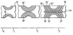
- FIGS. 3A and 3Bshow heat affected zones as a result of ablating a target material from both sides thereof to create a through hole.
- FIG. 4show heat affected zones over periods of time as a result of ablating a target material from both sides thereof to create a through hole.
- the laser system 10includes a IR laser 12 having a resonator cavity 14 which comprises a lasant 16 positioned between a highly reflective mirror 18 and a partially transmissive mirror (or output coupler) 20 along a beam path 22 .
- the lasant 16 in the resonator cavity 14is preferably a solid-state laser rod comprising Nd:YAG, Nd:YAP, Nd:YVO 4 .
- solid-state lasants or even gas, semiconductor or tunable organic dye lasantscould be used in the lasers 12 .
- suitable gas lasants and their fundamental wavelengthscould include Nitrogen (337.1 nm), HeCd (325.0-441.6 nm), Argon (457.9-514.5 nm), Krypton (350.7-799.3 nm), HeNe (632 nm), CO (4.0 ⁇ 10 3 -5.5 ⁇ 10 3 nm), CO 2 (10.6 ⁇ 10 3 nm), and H 2 O (118.3 ⁇ 10 3 nm).
- suitable solid-state lasantscould include Ruby (694.3 nm), Nd:Glass (1.06 ⁇ 10 3 nm), Nd:YAG (1.06 ⁇ 10 3 nm), Nd:YAP (1.06 ⁇ 10 3 nm), and Nd:YVO 4
- suitable semiconductor lasantscould include GaAs (904 nm for a single diode or 850 ⁇ 50 nm for an array of 48 diodes).
- Laser rod 16may be pumped by a variety of pumping sources (not shown) well known to persons skilled in the art, such as thermal, electrical or optical. However, a suitable diode pump or arc lamp is preferred for the illustrated Neodymium based laser system.
- the resonator cavity 14is illustrated with an associated Q-switch 24 which preferably operates by electro-optical or accusto-optical means.
- Q-switch 24which preferably operates by electro-optical or accusto-optical means.
- Other well known laser componentse.g., polarizers, limiting apertures, attenuators and the like
- their uses, positioning, and operationare well known to those skilled in the art and could be utilized inside the resonator cavities as desired.
- the IR output from the resonator 14is passed through an upcollimator structure 28 , after which it is deflected downwardly along a beam path 30 by a beam-directing reflector 32 into a focusing lens 34 and then to an electronic component material.
- the electronic component materialis silicone or a multi-layered target 36 .
- any suitable lasercan be employed such as a green laser to produce green light (e.g., between about 500 nm to about 580 nm), a UV laser (e.g., UV light at harmonics of 1064 nm fundamental wavelength) or a multiple wavelength laser (e.g., EM radiation at a fundamental wavelength of 1064 nm).
- a green laser to produce green lighte.g., between about 500 nm to about 580 nm
- a UV lasere.g., UV light at harmonics of 1064 nm fundamental wavelength
- a multiple wavelength lasere.g., EM radiation at a fundamental wavelength of 1064 nm
- the multi-layered target 36can be, for example, a circuit board with a top conductor layer 27 , an upper dielectric layer 29 , an embedded conductor layer 31 , a lower dielectric layer 33 , and a bottom conductor layer 35 , respectively.
- the conductor layersmay comprise conductive metals such as copper, aluminum, titanium, nickel, tungsten, platinum, gold, molybdenum, palladium, silver, or combinations thereof.
- the dielectric layersmay comprise an organic composition such as PTFE, polyimides, epoxies, or combinations thereof.
- the dielectric materialsmay be reinforced with glass fibers, aramid fibers, KEVLAR, ceramics, or combinations thereof.
- the conductor layersare preferably copper and dielectric layers are either RCC or FR4, both of which contain epoxy, an organic dielectric material. FR4 also contains glass reinforcement. It should be apparent that these construction used in the PCB manufacturing are only examples of dielectric conductor layers used to form circuits. The example is only one of a multitude of constructions.
- the laser system 10is preferably used to create vias, e.g., blind or through holes in the electronic component material or target 36 , such as a circuit board.
- machining of the target with a laser system 10can occur from all or various degrees of freedom, e.g., top, bottom, and sides of the target 36 .
- a laser system 10produces a laser light beam 38 that is split by beam splitter 40 into an upper light beam 42 and a lower light beam 44 .
- the upper light beampasses through an optical diffuser 46 and ablates the target 36 at an upper portion 47 thereof at a certain fluence and power density.
- the lower light beam 44passes through another optical diffuser 48 and ablates a lower portion 49 of the target 36 at certain fluence and power density.
- the fluence and power density of the beams 42 and 44can be the same or can be different from each other. As shown in FIG. 2, the light beams 42 and 44 ablate different areas of the target 36 . It can be appreciated that the light beams 42 and 44 can be disposed along a common axis to cut a through hole in the target 36 .
- a first laser system 10 ′can be used to ablate from the upper surface of the target 36 and a second laser system 10 ′′ can be used to ablate from the lower portion of the target 36 . More particularly, the first laser system 10 ′ generates a light beam 50 that passes through an optical diffuser 52 to ablate from the top portion 47 of the target 36 . The second laser system 10 ′′ generates a second laser light beam 54 that passes through another optical diffuser 56 to ablate from the lower portion 49 of the target 36 . As shown, the light beams 50 and 54 are aligned axially to create a through hole in the target 36 . The thickness d of the target of FIG.
- the fluence and power densities of the beams 50 and 54can be the same or can be different from each other. It can be appreciated that the beams 54 and 50 need not be aligned axially when different areas of the target are to be ablated.
- FIG. 3Ashows an initial ablation from both the top and bottom of the target 36 .
- materialis removed and heat affected zones 58 are created at both the top and the bottom of the target 36 .
- a heat assist ablation zone 60is defined which allows for faster and more efficient laser ablation of the target 36 since ablation is then performed on material that is already heated.
- an initial ablationsimultaneously from both sides of a target 36 , at time t 0 results in material being removed and creation of initial heat affected zones 58 at time t 1 .
- a cooling periode.g., t 1 to t 2
- the heat affected zones 58 ′ in the target 36 materialhave diffused, covering a larger area.
- Another ablationis performed during time t 2 to t 3 at the top and bottom of the target 36 that results in the heat affected zone 62 along with heat assisted zone 64 . Since the further ablation is performed in the heat affected zones and the heat assisted zone is created, this technique results in faster and more efficient material removal while minimizing thermal loading of the target 36 .
- the light beams ablating the targetcan be located at different areas as in the left hand portion of FIG. 1 .
- a spatial serial processing techniquea first area of the target 36 is initially ablated. Thereafter, a second area is initially ablated while the first area is cooling. Once the initial ablation of the second area is complete, the first area can be further ablated. This process is continued until all areas are fully ablated. As a result, thermal loading of the target 36 is minimized.
- a low degree of thermal loadingis achieved by machining in distinct steps to allow the same amount of fluence to be transferred to the target 36 .
- the methods described aboveminimize thermal loading of the target 36 during machining of through holes or vias therein by working from the top of the target and from the bottom of the target generally simultaneously. Also, different areas of a target can be worked on at different times or time intervals to avoid threshold levels of thermal loading in the surrounding material of the target.
- the resulting structuresare better in quality and allow for improved manufacturing of the devices.
- the improvementis based on the adjustment of the energy density during the formation of structures i.e., vias, to accomplish:
- the laser and methods disclosed hereinare applicable to any laser process used to cut, weld, anneal or define shapes on electronic material.
- the specific electronic material of interestis silicone (used in integrated electronic circuits) and advanced electronic packages/PCBs composed of multiple layers of conductive and non-conductive layers.
- the methodis applicable to any lasers incorporated into laser systems that use a certain power density and fluence at the workpiece.
Landscapes
- Engineering & Computer Science (AREA)
- Physics & Mathematics (AREA)
- Optics & Photonics (AREA)
- Manufacturing & Machinery (AREA)
- Microelectronics & Electronic Packaging (AREA)
- Plasma & Fusion (AREA)
- Mechanical Engineering (AREA)
- Laser Beam Processing (AREA)
Abstract
Description
Claims (14)
Priority Applications (1)
| Application Number | Priority Date | Filing Date | Title |
|---|---|---|---|
| US10/120,029US6821472B2 (en) | 2002-04-10 | 2002-04-10 | Method of laser machining materials with minimal thermal loading |
Applications Claiming Priority (1)
| Application Number | Priority Date | Filing Date | Title |
|---|---|---|---|
| US10/120,029US6821472B2 (en) | 2002-04-10 | 2002-04-10 | Method of laser machining materials with minimal thermal loading |
Publications (2)
| Publication Number | Publication Date |
|---|---|
| US20030193117A1 US20030193117A1 (en) | 2003-10-16 |
| US6821472B2true US6821472B2 (en) | 2004-11-23 |
Family
ID=28790021
Family Applications (1)
| Application Number | Title | Priority Date | Filing Date |
|---|---|---|---|
| US10/120,029Expired - Fee RelatedUS6821472B2 (en) | 2002-04-10 | 2002-04-10 | Method of laser machining materials with minimal thermal loading |
Country Status (1)
| Country | Link |
|---|---|
| US (1) | US6821472B2 (en) |
Cited By (2)
| Publication number | Priority date | Publication date | Assignee | Title |
|---|---|---|---|---|
| US20060086701A1 (en)* | 2004-10-27 | 2006-04-27 | Daniel Perreault | Method of applying one or more electromagnetic beams to form a fusion bond on a workpiece such as a medical device |
| US20090223942A1 (en)* | 2005-06-30 | 2009-09-10 | Jon Heyl | Lead Frame Isolation Using Laser Technology |
Families Citing this family (8)
| Publication number | Priority date | Publication date | Assignee | Title |
|---|---|---|---|---|
| US7310205B2 (en)* | 2004-09-30 | 2007-12-18 | Hitachi Global Storage Technologies Netherlands, B.V. | Thermally assisted recording of magnetic media using a resonant cavity and energy |
| US7236332B2 (en)* | 2004-10-22 | 2007-06-26 | Hitachi Global Storage Technologies Netherlands, B.V. | Thermally assisted recording of magnetic using an in-gap optical resonant cavity |
| US7365941B2 (en)* | 2005-01-24 | 2008-04-29 | Hitachi Global Storage Technologies Netherlands, B.V. | Optical recording head including an optical resonant cavity |
| US20080029152A1 (en)* | 2006-08-04 | 2008-02-07 | Erel Milshtein | Laser scribing apparatus, systems, and methods |
| WO2020245956A1 (en)* | 2019-06-05 | 2020-12-10 | 三菱重工業株式会社 | Laser machining method and laser machining device |
| US20210310122A1 (en)* | 2020-04-03 | 2021-10-07 | Applied Materials, Inc. | Method of forming holes from both sides of substrate |
| US11819948B2 (en)* | 2020-10-14 | 2023-11-21 | Applied Materials, Inc. | Methods to fabricate chamber component holes using laser drilling |
| US12030135B2 (en)* | 2020-10-14 | 2024-07-09 | Applied Materials, Inc. | Methods to fabricate chamber component holes using laser drilling |
Citations (22)
| Publication number | Priority date | Publication date | Assignee | Title |
|---|---|---|---|---|
| US3989778A (en) | 1975-12-17 | 1976-11-02 | W. R. Grace & Co. | Method of heat sealing thermoplastic sheets together using a split laser beam |
| US4224096A (en) | 1976-03-25 | 1980-09-23 | W. R. Grace & Co. | Laser sealing of thermoplastic material |
| US4652721A (en)* | 1985-01-03 | 1987-03-24 | Dow Corning Corporation | Method and apparatus for edge contouring lenses |
| US4918284A (en) | 1988-10-14 | 1990-04-17 | Teradyne Laser Systems, Inc. | Calibrating laser trimming apparatus |
| JPH0357581A (en)* | 1989-07-27 | 1991-03-12 | Nec Corp | Laser beam welding machine |
| US5521352A (en) | 1993-09-23 | 1996-05-28 | Laser Machining, Inc. | Laser cutting apparatus |
| US5578229A (en) | 1994-10-18 | 1996-11-26 | Michigan State University | Method and apparatus for cutting boards using opposing convergent laser beams |
| US5590854A (en)* | 1994-11-02 | 1997-01-07 | Shatz; Solomon | Movable sheet for laminar flow and deicing |
| US5595791A (en) | 1993-11-10 | 1997-01-21 | International Business Machines Corporation | Process for texturing brittle glass disks |
| US5643472A (en) | 1988-07-08 | 1997-07-01 | Cauldron Limited Partnership | Selective removal of material by irradiation |
| US5874011A (en) | 1996-08-01 | 1999-02-23 | Revise, Inc. | Laser-induced etching of multilayer materials |
| US5883356A (en) | 1996-05-13 | 1999-03-16 | Tip Engineering Group, Inc. | Laser scoring process and apparatus |
| US5981902A (en) | 1994-12-15 | 1999-11-09 | Mitsubishi Chemical Corporation | Texturing apparatus for magnetic recording medium and magnetic recording medium process thereby |
| US5981903A (en) | 1997-03-28 | 1999-11-09 | International Business Machines Corporation | Laser system for simultaneous texturing of two sides of a substrate |
| US6087625A (en) | 1997-03-21 | 2000-07-11 | Sumitomo Heavy Industries, Ltd. | Laser machining apparatus |
| US6128199A (en) | 1997-03-19 | 2000-10-03 | Rohm Co., Ltd. | Composite device and manufacturing method thereof |
| US6156030A (en) | 1997-06-04 | 2000-12-05 | Y-Beam Technologies, Inc. | Method and apparatus for high precision variable rate material removal and modification |
| US6207926B1 (en) | 1997-01-15 | 2001-03-27 | Seagate Technology Llc | Fiber optic laser texturing with optical probe feedback control |
| US6291794B1 (en) | 1999-10-19 | 2001-09-18 | Lsp Technologies, Inc. | Multiple beam time sharing for a laser shock peening apparatus |
| US20010035401A1 (en) | 1999-06-08 | 2001-11-01 | Ran Manor | Dual laser cutting of wafers |
| US20020000426A1 (en) | 2000-01-25 | 2002-01-03 | Mead Roy D. | Use of multiple laser sources for rapid, flexible machining and production of vias in multi-layered substrates |
| US20020170891A1 (en)* | 2001-03-22 | 2002-11-21 | Adrian Boyle | Laser machining system and method |
- 2002
- 2002-04-10USUS10/120,029patent/US6821472B2/ennot_activeExpired - Fee Related
Patent Citations (23)
| Publication number | Priority date | Publication date | Assignee | Title |
|---|---|---|---|---|
| US3989778A (en) | 1975-12-17 | 1976-11-02 | W. R. Grace & Co. | Method of heat sealing thermoplastic sheets together using a split laser beam |
| US4224096A (en) | 1976-03-25 | 1980-09-23 | W. R. Grace & Co. | Laser sealing of thermoplastic material |
| US4652721A (en)* | 1985-01-03 | 1987-03-24 | Dow Corning Corporation | Method and apparatus for edge contouring lenses |
| US5643472A (en) | 1988-07-08 | 1997-07-01 | Cauldron Limited Partnership | Selective removal of material by irradiation |
| US4918284A (en) | 1988-10-14 | 1990-04-17 | Teradyne Laser Systems, Inc. | Calibrating laser trimming apparatus |
| JPH0357581A (en)* | 1989-07-27 | 1991-03-12 | Nec Corp | Laser beam welding machine |
| US5521352A (en) | 1993-09-23 | 1996-05-28 | Laser Machining, Inc. | Laser cutting apparatus |
| US5595791A (en) | 1993-11-10 | 1997-01-21 | International Business Machines Corporation | Process for texturing brittle glass disks |
| US6246543B1 (en) | 1993-11-10 | 2001-06-12 | International Business Machines Corporation | Textured data storage disk having a brittle nonmetallic substrate |
| US5578229A (en) | 1994-10-18 | 1996-11-26 | Michigan State University | Method and apparatus for cutting boards using opposing convergent laser beams |
| US5590854A (en)* | 1994-11-02 | 1997-01-07 | Shatz; Solomon | Movable sheet for laminar flow and deicing |
| US5981902A (en) | 1994-12-15 | 1999-11-09 | Mitsubishi Chemical Corporation | Texturing apparatus for magnetic recording medium and magnetic recording medium process thereby |
| US5883356A (en) | 1996-05-13 | 1999-03-16 | Tip Engineering Group, Inc. | Laser scoring process and apparatus |
| US5874011A (en) | 1996-08-01 | 1999-02-23 | Revise, Inc. | Laser-induced etching of multilayer materials |
| US6207926B1 (en) | 1997-01-15 | 2001-03-27 | Seagate Technology Llc | Fiber optic laser texturing with optical probe feedback control |
| US6128199A (en) | 1997-03-19 | 2000-10-03 | Rohm Co., Ltd. | Composite device and manufacturing method thereof |
| US6087625A (en) | 1997-03-21 | 2000-07-11 | Sumitomo Heavy Industries, Ltd. | Laser machining apparatus |
| US5981903A (en) | 1997-03-28 | 1999-11-09 | International Business Machines Corporation | Laser system for simultaneous texturing of two sides of a substrate |
| US6156030A (en) | 1997-06-04 | 2000-12-05 | Y-Beam Technologies, Inc. | Method and apparatus for high precision variable rate material removal and modification |
| US20010035401A1 (en) | 1999-06-08 | 2001-11-01 | Ran Manor | Dual laser cutting of wafers |
| US6291794B1 (en) | 1999-10-19 | 2001-09-18 | Lsp Technologies, Inc. | Multiple beam time sharing for a laser shock peening apparatus |
| US20020000426A1 (en) | 2000-01-25 | 2002-01-03 | Mead Roy D. | Use of multiple laser sources for rapid, flexible machining and production of vias in multi-layered substrates |
| US20020170891A1 (en)* | 2001-03-22 | 2002-11-21 | Adrian Boyle | Laser machining system and method |
Cited By (4)
| Publication number | Priority date | Publication date | Assignee | Title |
|---|---|---|---|---|
| US20060086701A1 (en)* | 2004-10-27 | 2006-04-27 | Daniel Perreault | Method of applying one or more electromagnetic beams to form a fusion bond on a workpiece such as a medical device |
| US7820937B2 (en)* | 2004-10-27 | 2010-10-26 | Boston Scientific Scimed, Inc. | Method of applying one or more electromagnetic beams to form a fusion bond on a workpiece such as a medical device |
| US20090223942A1 (en)* | 2005-06-30 | 2009-09-10 | Jon Heyl | Lead Frame Isolation Using Laser Technology |
| US8198137B2 (en)* | 2005-06-30 | 2012-06-12 | Jon Heyl | Lead frame isolation using laser technology |
Also Published As
| Publication number | Publication date |
|---|---|
| US20030193117A1 (en) | 2003-10-16 |
Similar Documents
| Publication | Publication Date | Title |
|---|---|---|
| US6911622B2 (en) | Laser processing | |
| EP0900132B1 (en) | Method employing uv laser pulses of varied energy density to form blind vias in multilayered targets | |
| US7679030B2 (en) | Energy-efficient, laser-based method and system for processing target material | |
| US6791060B2 (en) | Beam shaping and projection imaging with solid state UV gaussian beam to form vias | |
| JP2007508946A (en) | Laser processing of locally heated target materials | |
| US6821472B2 (en) | Method of laser machining materials with minimal thermal loading | |
| KR100670841B1 (en) | Switchable Wavelength Laser Based Etch Circuit Board Processing System | |
| JP3138954B2 (en) | Via hole formation method | |
| US6577448B2 (en) | Laser system by modulation of power and energy | |
| JP2007029952A (en) | Laser beam machining apparatus, and laser beam machining method | |
| JP2005028369A (en) | Laser beam machining method | |
| JP2003285183A (en) | Laser beam machining device and machining method | |
| JP3343812B2 (en) | Via hole forming method and laser processing apparatus | |
| WO2001014096A1 (en) | Multiple ultraviolet beam solid-state laser systems and methods | |
| JP2000271774A (en) | Method and device of desmearing for laser beam piercing device | |
| KR20070091052A (en) | Energy-efficient laser-based method and system for target processing | |
| Patil | Design study of UV laser & Effects and comparison of UV laser and CO2 on the profile cutting of flexible circuit | |
| CA2246329A1 (en) | Method employing uv laser pulses of varied energy density to form blind vias in multilayered targets |
Legal Events
| Date | Code | Title | Description |
|---|---|---|---|
| AS | Assignment | Owner name:SIEMENS DEMATIC ELECTRONICS ASSEMBLY SYSTEMS, INC. Free format text:ASSIGNMENT OF ASSIGNORS INTEREST;ASSIGNORS:SCHRIENER, ALEXANDER F.;HOFMANN, NEAL;REEL/FRAME:013041/0009 Effective date:20020613 | |
| AS | Assignment | Owner name:SIEMENS DEMATIC AKTIENGESELLSCHAFT, GERMANY Free format text:ASSIGNMENT OF ASSIGNORS INTEREST;ASSIGNOR:SIEMENS DEMATIC ELECTRONICS ASSEMBLY SYSTEMS, INC.;REEL/FRAME:012839/0835 Effective date:20020614 | |
| FPAY | Fee payment | Year of fee payment:4 | |
| AS | Assignment | Owner name:SIEMENS ELECTRONICS ASSEMBLY SYSTEMS GMBH & CO. KG Free format text:ASSIGNMENT OF ASSIGNORS INTEREST;ASSIGNOR:SIEMENS AKTIENGESELLSCHAFT, INC.;REEL/FRAME:022868/0581 Effective date:20090625 Owner name:SIEMENS AKTIENGESELLSCHAFT, GERMANY Free format text:MERGER;ASSIGNOR:SIEMENS DEMATIC AKTIENGESELLSCHAFT;REEL/FRAME:022868/0577 Effective date:20080331 | |
| REMI | Maintenance fee reminder mailed | ||
| LAPS | Lapse for failure to pay maintenance fees | ||
| STCH | Information on status: patent discontinuation | Free format text:PATENT EXPIRED DUE TO NONPAYMENT OF MAINTENANCE FEES UNDER 37 CFR 1.362 | |
| FP | Lapsed due to failure to pay maintenance fee | Effective date:20121123 |