US6820328B2 - Method of removing heat from an electronic assemblage - Google Patents
Method of removing heat from an electronic assemblageDownload PDFInfo
- Publication number
- US6820328B2 US6820328B2US10/328,337US32833702AUS6820328B2US 6820328 B2US6820328 B2US 6820328B2US 32833702 AUS32833702 AUS 32833702AUS 6820328 B2US6820328 B2US 6820328B2
- Authority
- US
- United States
- Prior art keywords
- heat
- thermally conductive
- generating component
- heat generating
- conductive material
- Prior art date
- Legal status (The legal status is an assumption and is not a legal conclusion. Google has not performed a legal analysis and makes no representation as to the accuracy of the status listed.)
- Expired - Lifetime, expires
Links
Images


Classifications
- H—ELECTRICITY
- H05—ELECTRIC TECHNIQUES NOT OTHERWISE PROVIDED FOR
- H05K—PRINTED CIRCUITS; CASINGS OR CONSTRUCTIONAL DETAILS OF ELECTRIC APPARATUS; MANUFACTURE OF ASSEMBLAGES OF ELECTRICAL COMPONENTS
- H05K1/00—Printed circuits
- H05K1/02—Details
- H05K1/0201—Thermal arrangements, e.g. for cooling, heating or preventing overheating
- H05K1/0203—Cooling of mounted components
- H05K1/0204—Cooling of mounted components using means for thermal conduction connection in the thickness direction of the substrate
- H05K1/0206—Cooling of mounted components using means for thermal conduction connection in the thickness direction of the substrate by printed thermal vias
- H—ELECTRICITY
- H05—ELECTRIC TECHNIQUES NOT OTHERWISE PROVIDED FOR
- H05K—PRINTED CIRCUITS; CASINGS OR CONSTRUCTIONAL DETAILS OF ELECTRIC APPARATUS; MANUFACTURE OF ASSEMBLAGES OF ELECTRICAL COMPONENTS
- H05K2201/00—Indexing scheme relating to printed circuits covered by H05K1/00
- H05K2201/02—Fillers; Particles; Fibers; Reinforcement materials
- H05K2201/0203—Fillers and particles
- H05K2201/0206—Materials
- H05K2201/0209—Inorganic, non-metallic particles
- H—ELECTRICITY
- H05—ELECTRIC TECHNIQUES NOT OTHERWISE PROVIDED FOR
- H05K—PRINTED CIRCUITS; CASINGS OR CONSTRUCTIONAL DETAILS OF ELECTRIC APPARATUS; MANUFACTURE OF ASSEMBLAGES OF ELECTRICAL COMPONENTS
- H05K2201/00—Indexing scheme relating to printed circuits covered by H05K1/00
- H05K2201/09—Shape and layout
- H05K2201/09209—Shape and layout details of conductors
- H05K2201/095—Conductive through-holes or vias
- H05K2201/0959—Plated through-holes or plated blind vias filled with insulating material
- H—ELECTRICITY
- H05—ELECTRIC TECHNIQUES NOT OTHERWISE PROVIDED FOR
- H05K—PRINTED CIRCUITS; CASINGS OR CONSTRUCTIONAL DETAILS OF ELECTRIC APPARATUS; MANUFACTURE OF ASSEMBLAGES OF ELECTRICAL COMPONENTS
- H05K2201/00—Indexing scheme relating to printed circuits covered by H05K1/00
- H05K2201/09—Shape and layout
- H05K2201/09209—Shape and layout details of conductors
- H05K2201/09654—Shape and layout details of conductors covering at least two types of conductors provided for in H05K2201/09218 - H05K2201/095
- H05K2201/09781—Dummy conductors, i.e. not used for normal transport of current; Dummy electrodes of components
- H—ELECTRICITY
- H05—ELECTRIC TECHNIQUES NOT OTHERWISE PROVIDED FOR
- H05K—PRINTED CIRCUITS; CASINGS OR CONSTRUCTIONAL DETAILS OF ELECTRIC APPARATUS; MANUFACTURE OF ASSEMBLAGES OF ELECTRICAL COMPONENTS
- H05K2201/00—Indexing scheme relating to printed circuits covered by H05K1/00
- H05K2201/09—Shape and layout
- H05K2201/09209—Shape and layout details of conductors
- H05K2201/09654—Shape and layout details of conductors covering at least two types of conductors provided for in H05K2201/09218 - H05K2201/095
- H05K2201/0979—Redundant conductors or connections, i.e. more than one current path between two points
- H—ELECTRICITY
- H05—ELECTRIC TECHNIQUES NOT OTHERWISE PROVIDED FOR
- H05K—PRINTED CIRCUITS; CASINGS OR CONSTRUCTIONAL DETAILS OF ELECTRIC APPARATUS; MANUFACTURE OF ASSEMBLAGES OF ELECTRICAL COMPONENTS
- H05K3/00—Apparatus or processes for manufacturing printed circuits
- H05K3/0058—Laminating printed circuit boards onto other substrates, e.g. metallic substrates
- H05K3/0061—Laminating printed circuit boards onto other substrates, e.g. metallic substrates onto a metallic substrate, e.g. a heat sink
- H—ELECTRICITY
- H05—ELECTRIC TECHNIQUES NOT OTHERWISE PROVIDED FOR
- H05K—PRINTED CIRCUITS; CASINGS OR CONSTRUCTIONAL DETAILS OF ELECTRIC APPARATUS; MANUFACTURE OF ASSEMBLAGES OF ELECTRICAL COMPONENTS
- H05K3/00—Apparatus or processes for manufacturing printed circuits
- H05K3/40—Forming printed elements for providing electric connections to or between printed circuits
- H05K3/42—Plated through-holes or plated via connections
- H05K3/429—Plated through-holes specially for multilayer circuits, e.g. having connections to inner circuit layers
- Y—GENERAL TAGGING OF NEW TECHNOLOGICAL DEVELOPMENTS; GENERAL TAGGING OF CROSS-SECTIONAL TECHNOLOGIES SPANNING OVER SEVERAL SECTIONS OF THE IPC; TECHNICAL SUBJECTS COVERED BY FORMER USPC CROSS-REFERENCE ART COLLECTIONS [XRACs] AND DIGESTS
- Y10—TECHNICAL SUBJECTS COVERED BY FORMER USPC
- Y10T—TECHNICAL SUBJECTS COVERED BY FORMER US CLASSIFICATION
- Y10T29/00—Metal working
- Y10T29/49—Method of mechanical manufacture
- Y10T29/49002—Electrical device making
- Y10T29/49117—Conductor or circuit manufacturing
- Y10T29/49124—On flat or curved insulated base, e.g., printed circuit, etc.
- Y10T29/4913—Assembling to base an electrical component, e.g., capacitor, etc.
- Y10T29/49144—Assembling to base an electrical component, e.g., capacitor, etc. by metal fusion
- Y—GENERAL TAGGING OF NEW TECHNOLOGICAL DEVELOPMENTS; GENERAL TAGGING OF CROSS-SECTIONAL TECHNOLOGIES SPANNING OVER SEVERAL SECTIONS OF THE IPC; TECHNICAL SUBJECTS COVERED BY FORMER USPC CROSS-REFERENCE ART COLLECTIONS [XRACs] AND DIGESTS
- Y10—TECHNICAL SUBJECTS COVERED BY FORMER USPC
- Y10T—TECHNICAL SUBJECTS COVERED BY FORMER US CLASSIFICATION
- Y10T29/00—Metal working
- Y10T29/49—Method of mechanical manufacture
- Y10T29/49002—Electrical device making
- Y10T29/49117—Conductor or circuit manufacturing
- Y10T29/49124—On flat or curved insulated base, e.g., printed circuit, etc.
- Y10T29/49155—Manufacturing circuit on or in base
- Y10T29/49165—Manufacturing circuit on or in base by forming conductive walled aperture in base
Definitions
- the inventionrelates generally to the field of broad electronic technology (BET), and in particular to thermal management of highly dense circuit boards. More specifically, the invention relates to a method of reducing the heat of heat-generating electronic components during service.
- BETbroad electronic technology
- an electronic assemblagehas a heat-removing element associated with a heat-generating element for reducing the junction temperature of the heat-generating component by means of a plurality of thermal vias.
- a method of removing heat from a densely packed electronic assemblagecomprises a densely packed electronic assemblage comprising a substrate medium for supporting at least one heat generating component thereon.
- the heat-generating componenthas a characteristic junction temperature T j .
- a first heat removing element having a plurality of thermal viasis thermally associated with the heat generating component and reduces the junction temperature T j of the heat generating component.
- the heat-removing elementis spaced apart from the heat-generating component so as to produce an open space nearest to the heat-generating component for accommodating high density electrical layouts.
- a heat sink in fluid communications with the first heat removing elementabsorbs heat from the heat generating component and thereby reduces its junction temperature T j to a temperature T l , wherein T l is less than T j .
- the present inventionhas numerous advantages over prior art developments. More particularly, the densely packed electronic assemblage of the invention operates at lower temperatures and is, therefore, more reliable. Further, the electronic assemblage can allocate space in proximity to the heat-generating element for specific electrical traces essential for the design layout. Furthermore, the electronic assemblage of the invention may contain a larger number of standard and thinner width size components.
- FIG. 1is a plane view of a portion of an electronic assemblage in accordance with the invention
- FIG. 2is a cross-sectional view of an electronic assemblage in accordance with the invention.
- FIG. 3is an enlarged partial sectional view of an electronic assemblage of the invention.
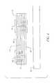
- FIG. 4is a cross-sectional view of a multi-layer circuit board containing a first and a fourth heat removing element.
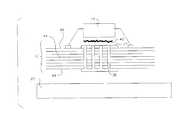
- electronic assemblage 10 of the inventionhas a substrate medium 12 , or typically a circuit board, having mounted thereon at least one heat generating components 14 , 30 .
- Heat generating component 14may include any number of components that generate heat during operations or under load, such as resistors, diodes, transistors, processors, etc. Skilled artisans will appreciate that each heat generating component 14 has a characteristic junction temperature T j , i.e., the die temperature during operation. During operations, as the heat generating component 14 approaches its maximum junction temperature, the prospect for component failure, and thus reliability problems becomes eminent.
- each heat generating component 14 in the electronic assemblage 10be associated with a novel and unobvious at least first heat removing element 16 for reducing the junction temperature T j of the heat generating component 14 to a temperature T l , where T l is considerably less than T j .
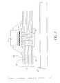
- First heat removing element 16comprising a plurality of patterned thermal vias 24 , forms a conduction path for carrying heat away from heat generating component 14 , as described further below.
- a heat sink 20is preferably associated with first heat removing element 16 . Heat sink 20 absorbs and transfers heat transported between the conduction path and the heat generating component 14 . In this way, excess heat from overheated heat generating component 14 is continually directed away from the electronic assemblage 10 , thereby preserving the reliability and performance of the electronic assemblage 10 and any heat sensitive component therein.
- substrate medium 12 of electronic assemblage 10may be a multi-layer circuit board, e.g., a 14-layer polyimide circuit board that uses 1 oz. copper on the inner layers 44 and 2 oz. copper on the outermost layers 46 , 48 .
- any circuit board materialis contemplated by the invention, since the primary heat transfer mechanism is thermal conduction via the plurality of thermal vias 24 of heat removal element 16 .
- substrate medium 12uses copper as the base trace 50 with a plating of nickel gold (NiAu).
- NiAunickel gold
- Current industry standards for platinginclude palladium (Pd), nickel gold (NiAu), Immersion Tin, Immersion silver, and hot air solder level (HASL).
- Pdpalladium
- NiAunickel gold
- HSLhot air solder level
- the specific circuit board material used in the present inventionis polyimide, it is of utmost importance that the thermal vias 24 of first heat removing element 16 can be drilled into the substrate medium 12 . Additional materials that can be used as substrate medium 12 with similar success include assorted resins and resin composites.
- any signal copper trace or power tracemay be utilized for the connecting path from heat generating component 14 to the thermal vias 24 of first heat removing element 16 .
- a particular pattern of thermal vias 24 in first heat removing element 16is arranged remotely from the heat generating component 14 .
- a third heat removing element 32 with thermal vias 34may also be positioned on a remote portion 18 of the substrate medium 12 away from the heat generating component 14 .
- Third heat removing element 32may alternatively be connected back to the first heat removing element 16 by connecting path 28 .
- first heat removing element 16is positioned proximate to the heat generating component 14 .
- first heat removing element 16provides a specific cross-sectional area with thermal vias 24 to conduct heat from the topmost surface 46 to the bottommost surface 48 of the circuit board 12 (see FIG. 3 ).
- the final thermal transfer from the heat generating component 14 to the heat sink 20takes place in the presence of a thermally conductive adhesive 40 .
- multiple remotely positioned first and third heat removing elements 16 , 32may be associated with a single heat generating component 14 to improve heat transport.
- multiple first and third heat removing elements 16 , 32may be associated with multiple heat generating components, e.g., first and second heat generating components 14 , 30 (shown in FIG. 1 ), to provide a dual heat transport system.
- first heat removing element 16may contain any number or size of thermal vias 24 to provide a conduction path between the outermost surfaces 46 , 48 of the substrate medium or circuit board 12 to facilitate and improve the thermal management.
- heat-removing element 16has a single group of thermal vias 24 remotely spaced about 1.0 inch away from the heat generating component 14 on substrate medium 12 . It should be appreciated that a remote first heat removing element 16 having thermal vias 24 may be arranged in any number of patches or arrays and may be situated practically any distance away from the heat generating component 14 , although closer is generally better.
- Thermal conduction paths contemplated by the inventioninclude electrical connections, non-electrical thermal connections, a fluid material connection between the heat generating component and first heat removing element, and surface bus wires, etc.
- first heat removing element 16is comprised of a plurality of regularly spaced thermal vias 24 formed in the substrate medium 12 .
- Thermal vias 24are generally round shaped and have a diameter of about 0.022 inches.
- each one of the thermal vias 24is spaced about 0.040 inches apart for optimum effectiveness in transporting heat.
- the thermal vias 24are filled with a thermally conductive material 22 .
- Preferred materialsinclude a material selected from the group consisting of: tin-lead solder; silver solder; thermally conductive liquid silicon adhesive; and thermally conductive liquid epoxy adhesive.
- the same or another thermally conductive adhesive 40may be disposed in the open space 42 produced between the heat generating component 14 and the substrate medium 12 thereby thermally connecting the heat generating component 14 and the second heat removing element 17 with thermal vias 36 .
- an aluminum heat sink 20 about 0.090 inches thickis associated with the substrate medium or circuit board 12 .
- Heat sink 20is attached to substrate medium or circuit board 12 with a thermally conductive material 38 , preferably a Dow Corning silicone thermally conductive, electrically isolative adhesive (1-4174TM).
- This particular adhesive materialcomprises 7-mil glass beads to facilitate the finished bonding spacing between the circuit board 12 and the heat sink 20 .
- any metal heat sink 20 having a range of thicknessmay be used with substantially similar results.
- thermally conductive adhesiveincluding epoxies and sheet films
- any material that can bond any circuit board to any rigidizer with even a nominal thermal conductivitymay be used since the heat has the entire circuit card area to transfer through the adhesive.
- the first heat removing element 16 of the inventioncould still be used to reduce the heat of the heat generating components 14 thereon.
- thermally and electrically conductive adhesivesare within the contemplation of the invention.
- an electrically isolative adhesiveis used due to trace population on the bottom layer of the circuit board 12 . Otherwise a shorting path to the heat sink 20 will exist.
- an electrically homogeneous layer (or partial layer) with the same signal as the thermal vias 24may also be used.
- the thermal vias 54 of fourth heat removing element 52would pass through the circuit board 12 and electrical vias would terminate at some layer above bottommost layer 48 . It should be appreciated that this latter design is a more expensive board to manufacture, but one that enables the use of higher conductive (electrically or thermally) material since adhesives that are electrically conductive can be more thermally conductive.
- thermal vias 24 of first heat removing element 16may be filled with a solder material 22 (as described above) to increase the effectiveness of the thermal vias 24 in removing heat from the heat generating component 14 .
- the thermal vias 24 of first heat removing element 16may remain unfilled or may be filled with a different thermally conductive material.
- a hand application or a specially designed solder paste stencilmay be used.
- the specially designed solder paste stencilwould have increased cut-out size to allow for the extra volume of solder required to fill the holes during processing. The actual increase in size can be calculated by adding the volume of the thermal vias 24 of first heat removing element 16 to the normal volume of solder paste desired.
- the substrate medium or circuit boards 12can be made of any material and used for any industry.
- the components specifically addressedare large plastic or ceramic components with lead frames, such as quad flat packs or dips, but it is additionally suited to even higher I/O component packages such as BGAs of any type.
- this method of providing remote vias 24 for coolingwill dramatically reduce the junction temperatures of the heat generating components which will improve the life and reliability of the component and thus the board and module. This method is especially useful where there is minimal area underneath proximate to the component for thermal vias due to critical electrical routing requirements.
- first heat removing element 16remotely located relative to the heat generating component 14 will help any package, but is generally used on these more densely packed electrical components that are routing space critical.
- the thermal vias 24 of first heat reducing element 16are made as “thermally conductive” as possible with the addition of solder inside the through-opening, as previously described. Any diameter size via can be used, but the optimum size (copper area vs. cost of drilling smaller holes and more of them) is currently around 0.022 inches in diameter (finished size). Additionally any “circuit” or “net” can be used, but the optimum for most designs is the “ground” nets.
- the heat sink 20which is typically “grounded.” This is typical of a bonded board assembly, but can additionally be used in a wedge-lock or direct fastener to chassis configuration where the heat transport is restricted to the mounting to the frame, card guide, or chassis. Additionally, a thermal conductive, electrically isolative silicone adhesive was used directly under the component to maximize heat transfer from the case of the component to the underlying copper ground paths. For BGA type components, the term “lead” would be replaced with the word “ball.” Conceptually, it is the same—using the grounding copper nets on the board to transfer heat to a remote area where the thermal vias can be placed. The extra ground nets have an additional benefit in making the circuit board less “noisy” electrically, which minimizes cross-talk issues.
Landscapes
- Engineering & Computer Science (AREA)
- Microelectronics & Electronic Packaging (AREA)
- Cooling Or The Like Of Semiconductors Or Solid State Devices (AREA)
- Cooling Or The Like Of Electrical Apparatus (AREA)
Abstract
Description
Claims (15)
Priority Applications (1)
| Application Number | Priority Date | Filing Date | Title |
|---|---|---|---|
| US10/328,337US6820328B2 (en) | 2002-12-23 | 2002-12-23 | Method of removing heat from an electronic assemblage |
Applications Claiming Priority (1)
| Application Number | Priority Date | Filing Date | Title |
|---|---|---|---|
| US10/328,337US6820328B2 (en) | 2002-12-23 | 2002-12-23 | Method of removing heat from an electronic assemblage |
Publications (2)
| Publication Number | Publication Date |
|---|---|
| US20040117982A1 US20040117982A1 (en) | 2004-06-24 |
| US6820328B2true US6820328B2 (en) | 2004-11-23 |
Family
ID=32594437
Family Applications (1)
| Application Number | Title | Priority Date | Filing Date |
|---|---|---|---|
| US10/328,337Expired - LifetimeUS6820328B2 (en) | 2002-12-23 | 2002-12-23 | Method of removing heat from an electronic assemblage |
Country Status (1)
| Country | Link |
|---|---|
| US (1) | US6820328B2 (en) |
Cited By (7)
| Publication number | Priority date | Publication date | Assignee | Title |
|---|---|---|---|---|
| US20060157864A1 (en)* | 2005-01-12 | 2006-07-20 | Industrial Technology Research Institute | Electronic device package and method of manufacturing the same |
| US20080052902A1 (en)* | 2006-07-06 | 2008-03-06 | Samsung Electro-Mechanics Co., Ltd. | Printed circuit board and manufacturing method thereof |
| US8312624B1 (en)* | 2011-11-24 | 2012-11-20 | Kinsus Interconnect Technology Corp. | Method for manufacturing a heat dissipation structure of a printed circuit board |
| CN102905470A (en)* | 2011-07-28 | 2013-01-30 | 景硕科技股份有限公司 | Forming method of heat dissipation structure of circuit carrier plate |
| US20130322020A1 (en)* | 2011-02-14 | 2013-12-05 | Endress +Hauser Fmbh + Co. KG | Electronic device and protective element therefor for use in explosion endangered areas |
| US20140168903A1 (en)* | 2012-12-13 | 2014-06-19 | Nvidia Corporation | Passive cooling system integrated into a printed circuit board for cooling electronic components |
| US20160050771A1 (en)* | 2014-08-15 | 2016-02-18 | Unimicron Technology Corp. | Manufacturing method of circuit structure embedded with heat-dissipation block |
Families Citing this family (3)
| Publication number | Priority date | Publication date | Assignee | Title |
|---|---|---|---|---|
| IL177336A (en) | 2006-08-07 | 2013-05-30 | Hanita Metal Works Ltd | Chatter-resistant end mill |
| FR3073980A1 (en)* | 2017-11-23 | 2019-05-24 | Stmicroelectronics (Grenoble 2) Sas | ENCAPSULATION COVER FOR ELECTRONIC HOUSING AND METHOD OF MANUFACTURE |
| US11865629B2 (en) | 2021-11-04 | 2024-01-09 | Kennametal Inc. | Rotary cutting tool with high ramp angle capability |
Citations (8)
| Publication number | Priority date | Publication date | Assignee | Title |
|---|---|---|---|---|
| US5543661A (en) | 1994-05-31 | 1996-08-06 | Sumitomo Metal Ceramics Inc. | Semiconductor ceramic package with terminal vias |
| US5796170A (en) | 1996-02-15 | 1998-08-18 | Northern Telecom Limited | Ball grid array (BGA) integrated circuit packages |
| US5959356A (en)* | 1995-11-25 | 1999-09-28 | Samsung Electronics Co., Ltd. | Solder ball grid array carrier package with heat sink |
| US5982630A (en)* | 1997-11-06 | 1999-11-09 | Intel Corporation | Printed circuit board that provides improved thermal dissipation |
| US6031729A (en)* | 1999-01-08 | 2000-02-29 | Trw Inc. | Integral heater for reworking MCMS and other semiconductor components |
| US6032355A (en)* | 1998-04-22 | 2000-03-07 | World Wiser Electronics, Inc. | Method of forming thermal conductive structure on printed circuit board |
| US6160705A (en) | 1997-05-09 | 2000-12-12 | Texas Instruments Incorporated | Ball grid array package and method using enhanced power and ground distribution circuitry |
| US6414847B1 (en)* | 2001-04-09 | 2002-07-02 | Agilent Technologies, Inc. | Integral dielectric heatspreader |
- 2002
- 2002-12-23USUS10/328,337patent/US6820328B2/ennot_activeExpired - Lifetime
Patent Citations (8)
| Publication number | Priority date | Publication date | Assignee | Title |
|---|---|---|---|---|
| US5543661A (en) | 1994-05-31 | 1996-08-06 | Sumitomo Metal Ceramics Inc. | Semiconductor ceramic package with terminal vias |
| US5959356A (en)* | 1995-11-25 | 1999-09-28 | Samsung Electronics Co., Ltd. | Solder ball grid array carrier package with heat sink |
| US5796170A (en) | 1996-02-15 | 1998-08-18 | Northern Telecom Limited | Ball grid array (BGA) integrated circuit packages |
| US6160705A (en) | 1997-05-09 | 2000-12-12 | Texas Instruments Incorporated | Ball grid array package and method using enhanced power and ground distribution circuitry |
| US5982630A (en)* | 1997-11-06 | 1999-11-09 | Intel Corporation | Printed circuit board that provides improved thermal dissipation |
| US6032355A (en)* | 1998-04-22 | 2000-03-07 | World Wiser Electronics, Inc. | Method of forming thermal conductive structure on printed circuit board |
| US6031729A (en)* | 1999-01-08 | 2000-02-29 | Trw Inc. | Integral heater for reworking MCMS and other semiconductor components |
| US6414847B1 (en)* | 2001-04-09 | 2002-07-02 | Agilent Technologies, Inc. | Integral dielectric heatspreader |
Cited By (13)
| Publication number | Priority date | Publication date | Assignee | Title |
|---|---|---|---|---|
| US20060157864A1 (en)* | 2005-01-12 | 2006-07-20 | Industrial Technology Research Institute | Electronic device package and method of manufacturing the same |
| US7632707B2 (en)* | 2005-01-12 | 2009-12-15 | Industrial Technology Research Institute | Electronic device package and method of manufacturing the same |
| US7838333B2 (en) | 2005-01-12 | 2010-11-23 | Industrial Technology Research Institute | Electronic device package and method of manufacturing the same |
| US20080052902A1 (en)* | 2006-07-06 | 2008-03-06 | Samsung Electro-Mechanics Co., Ltd. | Printed circuit board and manufacturing method thereof |
| US7810232B2 (en)* | 2006-07-06 | 2010-10-12 | Samsung Electro-Mechanics Co., Ltd. | Method of manufacturing a circuit board |
| US20130322020A1 (en)* | 2011-02-14 | 2013-12-05 | Endress +Hauser Fmbh + Co. KG | Electronic device and protective element therefor for use in explosion endangered areas |
| CN102905470A (en)* | 2011-07-28 | 2013-01-30 | 景硕科技股份有限公司 | Forming method of heat dissipation structure of circuit carrier plate |
| CN102905470B (en)* | 2011-07-28 | 2015-07-29 | 景硕科技股份有限公司 | Forming method of heat dissipation structure of circuit carrier board |
| US8312624B1 (en)* | 2011-11-24 | 2012-11-20 | Kinsus Interconnect Technology Corp. | Method for manufacturing a heat dissipation structure of a printed circuit board |
| US20140168903A1 (en)* | 2012-12-13 | 2014-06-19 | Nvidia Corporation | Passive cooling system integrated into a printed circuit board for cooling electronic components |
| US9538633B2 (en)* | 2012-12-13 | 2017-01-03 | Nvidia Corporation | Passive cooling system integrated into a printed circuit board for cooling electronic components |
| US20160050771A1 (en)* | 2014-08-15 | 2016-02-18 | Unimicron Technology Corp. | Manufacturing method of circuit structure embedded with heat-dissipation block |
| US10433413B2 (en)* | 2014-08-15 | 2019-10-01 | Unimicron Technology Corp. | Manufacturing method of circuit structure embedded with heat-dissipation block |
Also Published As
| Publication number | Publication date |
|---|---|
| US20040117982A1 (en) | 2004-06-24 |
Similar Documents
| Publication | Publication Date | Title |
|---|---|---|
| US6930885B2 (en) | Densely packed electronic assemblage with heat removing element | |
| US6770967B2 (en) | Remote thermal vias for densely packed electrical assemblage | |
| US6882537B2 (en) | Electrical assemblage and method for removing heat locally generated therefrom | |
| US7738249B2 (en) | Circuitized substrate with internal cooling structure and electrical assembly utilizing same | |
| US6212076B1 (en) | Enhanced heat-dissipating printed circuit board package | |
| US5223741A (en) | Package for an integrated circuit structure | |
| US5459639A (en) | Printed circuit board assembly having high heat radiation property | |
| US6317326B1 (en) | Integrated circuit device package and heat dissipation device | |
| US5646373A (en) | Apparatus for improving the power dissipation of a semiconductor device | |
| US6972479B2 (en) | Package with stacked substrates | |
| JPH10125832A (en) | Heat conduction method and apparatus therefor | |
| JP2011139083A (en) | Multi-chip electronic package having laminate carrier and assembly of the package | |
| JPH09283695A (en) | Semiconductor mounting structure | |
| US8058723B2 (en) | Package structure in which coreless substrate has direct electrical connections to semiconductor chip and manufacturing method thereof | |
| US6820328B2 (en) | Method of removing heat from an electronic assemblage | |
| US6778398B2 (en) | Thermal-conductive substrate package | |
| EP0471938A1 (en) | High circuit density thermal carrier | |
| US6671176B1 (en) | Method of cooling heat-generating electrical components | |
| US7161240B2 (en) | Insitu-cooled electrical assemblage | |
| JPH07321471A (en) | Multilayer board | |
| JP6633151B2 (en) | Circuit module | |
| JPH07273462A (en) | Electronic part mounting substrate | |
| KR20140129804A (en) | Heat Dissipation | |
| KR19990064001A (en) | Electronic package with improved pad design | |
| KR102787140B1 (en) | Semiconductor and method of fabricating the same |
Legal Events
| Date | Code | Title | Description |
|---|---|---|---|
| AS | Assignment | Owner name:EASTMAN KODAK COMPANY, NEW YORK Free format text:ASSIGNMENT OF ASSIGNORS INTEREST;ASSIGNOR:BARCLEY, TINA P.;REEL/FRAME:013627/0327 Effective date:20021220 | |
| FEPP | Fee payment procedure | Free format text:PAYOR NUMBER ASSIGNED (ORIGINAL EVENT CODE: ASPN); ENTITY STATUS OF PATENT OWNER: LARGE ENTITY | |
| STCF | Information on status: patent grant | Free format text:PATENTED CASE | |
| FPAY | Fee payment | Year of fee payment:4 | |
| AS | Assignment | Owner name:CITICORP NORTH AMERICA, INC., AS AGENT, NEW YORK Free format text:SECURITY INTEREST;ASSIGNORS:EASTMAN KODAK COMPANY;PAKON, INC.;REEL/FRAME:028201/0420 Effective date:20120215 | |
| FPAY | Fee payment | Year of fee payment:8 | |
| FEPP | Fee payment procedure | Free format text:PAYOR NUMBER ASSIGNED (ORIGINAL EVENT CODE: ASPN); ENTITY STATUS OF PATENT OWNER: LARGE ENTITY Free format text:PAYER NUMBER DE-ASSIGNED (ORIGINAL EVENT CODE: RMPN); ENTITY STATUS OF PATENT OWNER: LARGE ENTITY | |
| AS | Assignment | Owner name:PAKON, INC., INDIANA Free format text:PATENT RELEASE;ASSIGNORS:CITICORP NORTH AMERICA, INC.;WILMINGTON TRUST, NATIONAL ASSOCIATION;REEL/FRAME:029913/0001 Effective date:20130201 Owner name:KODAK (NEAR EAST), INC., NEW YORK Free format text:PATENT RELEASE;ASSIGNORS:CITICORP NORTH AMERICA, INC.;WILMINGTON TRUST, NATIONAL ASSOCIATION;REEL/FRAME:029913/0001 Effective date:20130201 Owner name:KODAK PORTUGUESA LIMITED, NEW YORK Free format text:PATENT RELEASE;ASSIGNORS:CITICORP NORTH AMERICA, INC.;WILMINGTON TRUST, NATIONAL ASSOCIATION;REEL/FRAME:029913/0001 Effective date:20130201 Owner name:EASTMAN KODAK COMPANY, NEW YORK Free format text:PATENT RELEASE;ASSIGNORS:CITICORP NORTH AMERICA, INC.;WILMINGTON TRUST, NATIONAL ASSOCIATION;REEL/FRAME:029913/0001 Effective date:20130201 Owner name:KODAK REALTY, INC., NEW YORK Free format text:PATENT RELEASE;ASSIGNORS:CITICORP NORTH AMERICA, INC.;WILMINGTON TRUST, NATIONAL ASSOCIATION;REEL/FRAME:029913/0001 Effective date:20130201 Owner name:FAR EAST DEVELOPMENT LTD., NEW YORK Free format text:PATENT RELEASE;ASSIGNORS:CITICORP NORTH AMERICA, INC.;WILMINGTON TRUST, NATIONAL ASSOCIATION;REEL/FRAME:029913/0001 Effective date:20130201 Owner name:KODAK AVIATION LEASING LLC, NEW YORK Free format text:PATENT RELEASE;ASSIGNORS:CITICORP NORTH AMERICA, INC.;WILMINGTON TRUST, NATIONAL ASSOCIATION;REEL/FRAME:029913/0001 Effective date:20130201 Owner name:KODAK PHILIPPINES, LTD., NEW YORK Free format text:PATENT RELEASE;ASSIGNORS:CITICORP NORTH AMERICA, INC.;WILMINGTON TRUST, NATIONAL ASSOCIATION;REEL/FRAME:029913/0001 Effective date:20130201 Owner name:FPC INC., CALIFORNIA Free format text:PATENT RELEASE;ASSIGNORS:CITICORP NORTH AMERICA, INC.;WILMINGTON TRUST, NATIONAL ASSOCIATION;REEL/FRAME:029913/0001 Effective date:20130201 Owner name:LASER-PACIFIC MEDIA CORPORATION, NEW YORK Free format text:PATENT RELEASE;ASSIGNORS:CITICORP NORTH AMERICA, INC.;WILMINGTON TRUST, NATIONAL ASSOCIATION;REEL/FRAME:029913/0001 Effective date:20130201 Owner name:KODAK IMAGING NETWORK, INC., CALIFORNIA Free format text:PATENT RELEASE;ASSIGNORS:CITICORP NORTH AMERICA, INC.;WILMINGTON TRUST, NATIONAL ASSOCIATION;REEL/FRAME:029913/0001 Effective date:20130201 Owner name:CREO MANUFACTURING AMERICA LLC, WYOMING Free format text:PATENT RELEASE;ASSIGNORS:CITICORP NORTH AMERICA, INC.;WILMINGTON TRUST, NATIONAL ASSOCIATION;REEL/FRAME:029913/0001 Effective date:20130201 Owner name:NPEC INC., NEW YORK Free format text:PATENT RELEASE;ASSIGNORS:CITICORP NORTH AMERICA, INC.;WILMINGTON TRUST, NATIONAL ASSOCIATION;REEL/FRAME:029913/0001 Effective date:20130201 Owner name:QUALEX INC., NORTH CAROLINA Free format text:PATENT RELEASE;ASSIGNORS:CITICORP NORTH AMERICA, INC.;WILMINGTON TRUST, NATIONAL ASSOCIATION;REEL/FRAME:029913/0001 Effective date:20130201 Owner name:EASTMAN KODAK INTERNATIONAL CAPITAL COMPANY, INC., Free format text:PATENT RELEASE;ASSIGNORS:CITICORP NORTH AMERICA, INC.;WILMINGTON TRUST, NATIONAL ASSOCIATION;REEL/FRAME:029913/0001 Effective date:20130201 Owner name:KODAK AMERICAS, LTD., NEW YORK Free format text:PATENT RELEASE;ASSIGNORS:CITICORP NORTH AMERICA, INC.;WILMINGTON TRUST, NATIONAL ASSOCIATION;REEL/FRAME:029913/0001 Effective date:20130201 | |
| AS | Assignment | Owner name:APPLE INC., CALIFORNIA Free format text:ASSIGNMENT OF ASSIGNORS INTEREST;ASSIGNOR:EASTMAN KODAK COMPANY;REEL/FRAME:029939/0508 Effective date:20130211 | |
| FPAY | Fee payment | Year of fee payment:12 |