US6820248B1 - Method and apparatus for routing interconnects to devices with dissimilar pitches - Google Patents
Method and apparatus for routing interconnects to devices with dissimilar pitchesDownload PDFInfo
- Publication number
- US6820248B1 US6820248B1US10/075,178US7517802AUS6820248B1US 6820248 B1US6820248 B1US 6820248B1US 7517802 AUS7517802 AUS 7517802AUS 6820248 B1US6820248 B1US 6820248B1
- Authority
- US
- United States
- Prior art keywords
- pitch
- integrated circuit
- horizontal
- vertical
- core
- Prior art date
- Legal status (The legal status is an assumption and is not a legal conclusion. Google has not performed a legal analysis and makes no representation as to the accuracy of the status listed.)
- Expired - Lifetime, expires
Links
Images


Classifications
- G—PHYSICS
- G06—COMPUTING OR CALCULATING; COUNTING
- G06F—ELECTRIC DIGITAL DATA PROCESSING
- G06F30/00—Computer-aided design [CAD]
- G06F30/30—Circuit design
- G06F30/39—Circuit design at the physical level
- G06F30/394—Routing
Definitions
- the present inventionrelates generally to routing for devices with different pitch, and more particularly to routing of a core embedded in a programmable logic device where the core comprises a different pitch than the programmable logic device.
- Programmable logic devicesexist as a well-known type of integrated circuit that may be programmed by a user to perform specified logic functions.
- programmable logic devicessuch as programmable logic arrays (PLAs) and complex programmable logic devices (CPLDs).
- PLAsprogrammable logic arrays
- CPLDscomplex programmable logic devices
- FPGAfield programmable gate array
- An FPGAtypically includes an array of configurable logic blocks (CLBs) surrounded by a ring of programmable input/output blocks (IOBs).
- CLBs and IOBsare interconnected by a programmable interconnect structure.
- the CLBs, IOBs, and interconnect structureare typically programmed by loading a stream of configuration data (bitstream) into internal configuration memory cells that define how the CLBs, IOBs, and interconnect structure are configured.
- the configuration bitstreammay be read from an external memory, conventionally an external integrated circuit memory EEPROM, EPROM, PROM, and the like, though other types of memory may be used.
- the collective states of the individual memory cellsthen determine the function of the FPGA.
- Standard cellsare provided inside an FPGA as functional blocks and have a set height.
- standard cellis not to imply that any standard, de facto or otherwise, exists, as standard cell size may vary from company to company. So, for example, logic blocks, such as a flip-flop, a NAND gate, and an inverter, among other well-known logic circuits, each will lay out with a same height, but may have different lengths. This height is conventionally dependent on pitch of a company's integrated circuit process for one or more interconnect or metal layers.
- a standard cellmay be made up of several logic blocks, each with a same height, but possibly with different lengths. Thus, each standard cell will have a same height but may have varying lengths. Standard cells may be assembled for providing interconnectivity logic or “glue logic.” Thus, an FPGA may be connected to an embedded device to carry out complex tasks.
- an embedded device or coremay not have the same layout pitch as an FPGA.
- FPGA exclusive routing over an embedded corefurther complicates routing to an embedded core.
- a placement and routing database used by a routing programcreates routing for connecting an FPGA to an embedded core.
- non-equivalent pitch between such an FPGA and embedded corecauses design rule violations. These design rule violations heretofore were addressed by manual re-routing.
- checking a design for such violations and manually re-routingcan delay production by one or more months depending on complexity and number of connections between the FPGA and embedded core.
- An aspect of the present inventionis a method for configuring a routing program for routing connections between an integrated circuit device and an embedded core. More particularly, a first horizontal pitch and a first vertical pitch is obtained for one of the integrated circuit device and the embedded core, and a second horizontal pitch and a second vertical pitch is obtained for the other of the integrated circuit device and the embedded core, where the first vertical pitch and the second vertical pitch are not equal.
- a first connection layer inputincluding, but not limited to, the first vertical pitch and a horizontal direction, is provided to the routing program, and a second connection layer input, including, but not limited to, the second horizontal pitch and a vertical direction, is provided to the routing program.
- An aspect of the present inventionis an integrated circuit device comprising a first device coupled to a second device.
- the first devicecomprises a first horizontal pitch and a first vertical pitch.
- the second devicecomprises a second horizontal pitch and a second vertical pitch.
- At least one interconnect layeris for coupling the first device and the second device.
- the interconnect layercomprises a set of pitches selected from: (i) the first vertical pitch and the second horizontal pitch, and (ii) the first horizontal pitch and the second vertical pitch.
- FIG. 1is a block diagram of an exemplary embodiment of an integrated circuit comprising an FPGA, standard cells for glue logic and a microprocessor core in accordance with one or more aspects of the present invention.
- FIG. 2is a block diagram of an exemplary embodiment of integrated circuit device cores are formed on a semiconductor wafer of the prior art.
- FIGS. 3A and 3Bare line diagrams of respective exemplary portions of interconnect layers from the FPGA and the microprocessor core of FIG. 1 .
- FIG. 4is a cross-sectional diagram of exemplary portions of the FPGA and the microprocessor core of FIG. 1 .
- FIG. 5is a line diagram of an exemplary portion of an interconnect layer from the FPGA of FIG. 1 in accordance with an aspect of the present invention.
- FIG. 6is a cross-sectional diagram of an exemplary portion of the FPGA and the microprocessor core of FIG. 1 .
- FIG. 7is a flow diagram of an exemplary embodiment of a process in accordance with one or more aspects of the present invention
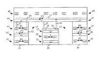
- FIG. 1there is shown a block diagram of an exemplary embodiment of an integrated circuit 100 comprising an FPGA 10 and a microprocessor core 20 in accordance with one or more aspects of the present invention.
- Grid 14is shown to indicated that a plurality of metal interconnect lines are used for connecting FPGA 10 circuitry to microprocessor core 20 circuitry.
- standard cells 19may be used to provide glue logic to connect FPGA circuitry 10 and microprocessor core 20 circuitry.
- Vias or contacts 16are formed to provide interconnection to desired locations of such circuitry and grid 14 .
- grid 14may comprise a plurality of interconnect layers, as described below in more detail.
- Microprocessor core 20comprises a plurality of pins 28 . Because pins may be longer than contact pads as indicated by vias 16 , there is more longitudinal variability for locating vias 16 to contact such pins 28 . Though pins 28 are shown as having a longitudinal or horizontal orientation, they may have a latitudinal or vertical orientation or a combination of both. However, for purposes of clarity of explanation, a horizontal orientation is described.
- a plurality of microprocessor cores 20is formed on a wafer 25 , as shown in the block diagram of FIG. 2 . Accordingly, there may be a region 15 between a microprocessor core 20 and an FPGA 10 , as shown in FIG. 1, as FPGA 10 may be formed with a different process flow than microprocessor core 20 . Region 15 may comprise standard cells 19 formed of one or more logic blocks 18 .
- FPGA 10is built proximal to microprocessor core 20 on a same wafer 25 or other substrate member upon which microprocessor core 20 is located.
- microprocessor core 20may have a different pitch for one or more of its interconnect layers than that of FPGA 10 . So, for example, suppose microprocessor core 20 was designed for a 0.13 micron process technology and laid out for a 0.57 micron horizontal and vertical pitch for its interconnect layers. And, suppose for example that FPGA 10 was designed for a 0.18 micron process technology and laid out for a 0.66 micron horizontal pitch and a 0.60 micron vertical pitch. Accordingly, automatic routing from microprocessor core 20 to FPGA 10 would be impracticable owing to design rule violations. To reduce such design rule violations with automatic routing, a neutral or compromise pitch set is employed.
- FIGS. 3A and 3Bwhere shown are line diagrams of respective exemplary portions of 30 and 31 of interconnect layers from FPGA 10 and microprocessor core 20 , respectively, of FIG. 1 .
- Grid portion 30comprises vertical conductive lines 11 and horizontal conductive lines 12 . Spacing between vertical conductive lines 11 is horizontal pitch H 1 , and spacing between horizontal conductive lines 12 is vertical pitch V 1 .
- Grid portion 31comprises vertical conductive lines 21 and horizontal conductive lines 22 . Spacing between vertical conductive lines 21 is horizontal pitch H 2 , and spacing between horizontal conductive lines 22 is vertical pitch V 2 .
- H 1 and V 1are 0.66 microns and 0.60 microns, respectively, and H 2 and V 2 are each 0.57 microns.
- FIG. 4there is shown a cross-sectional diagram of exemplary portions of FPGA 10 and microprocessor core 20 of FIG. 1 .
- FPGA 10is shown with five interconnect layers 41 , 42 , 43 , 44 and 45 , though fewer or more interconnect layers may be used.
- Microprocessor core 20is shown with three interconnect layers 51 , 52 and 53 , though fewer or more interconnect layers may be used.
- Region 15may comprise standard cells or a filler material, such as a dielectric, or a combination thereof.
- Vias 16are shown connecting pins 28 to conductive lines 11 and 12 .
- pins 28are conventionally connected to at least one of lines 21 and 22 , though not shown here for purposes of clarity.
- spacing or vertical pitch of pins 28is V 2 , as shown in FIG. 1 .
- interconnect layers 42 and 44As shown, a compromise pitch is used for interconnect layers 42 and 44 , namely, V 2 , which is the vertical pitch used for microprocessor core 20 conductive lines 22 and pins 28 .
- interconnect layers 41 , 43 and 45use a horizontal pitch H 1 from FPGA 10 layout.
- interconnect layers 42 and 44are on vertical pitch V 2 with pins 28 for connection thereto. This facilitates connecting to pins 28 without off-line line routing, namely, routing in between conductive lines, and thus reduces likelihood of design rule spacing violations.
- pins 28form a bus
- multiple vias 16may be used to connect to pins 28 to provide bus connectivity.
- FPGA 10retains horizontal pitch H 1 for layers 41 , 43 and 45 . This facilitates not violating design rules for FPGA 10 .
- vias 16may couple conductive lines 11 and 12 without violating design rules.
- FIG. 5there is shown a line diagram of an exemplary portion 50 of an interconnect layer from FPGA 10 in accordance with an aspect of the present invention.
- Conductive lines 12have a vertical pitch of V 2
- conductive lines 11have a horizontal pitch of H 1 .
- H 1may need to be substituted for H 2 .
- the present inventionmay be used to provide a pitch set (V 1 , H 2 ) for FPGA 10 .
- a plurality of interconnect layers of one pitch set(V 1 , H 2 ) are used for the vertically oriented pins, and another plurality of interconnect layers of another pitch set (V 2 , H 1 ) are used for the horizontally oriented pins.
- V 1 or H 1substitution of either V 1 or H 1 with V 2 or H 2 for FPGA 10 layout and routing is used for interconnect layers, namely, layers for interconnecting microprocessor core 20 to FPGA 10 . Though these interconnect layers may be used for FPGA location to FPGA location connectivity, other layers not used for interconnecting FPGA 10 to microprocessor core 20 may be present.
- FIG. 6there is shown a cross-sectional diagram of an exemplary portion of FPGA 10 and microprocessor core 20 in accordance with one or more aspects of the present invention.
- Metal layers 46 , 47 and 48are shown above interconnect layer 45 .
- Metal layers 46 , 47 and 48comprise pitches H 1 and V 1 .
- Use of FPGA 10 native pitches for non-interconnect layers to microprocessor core 20facilitates automatic routing without design rule spacing violation.
- step 71pitch from a first device is obtained or determined.
- step 72pitch from a second device is obtained.
- step 73pitch from the first device and pitch from the second device are provided to a database accessible by a routing program.
- the routing programis run using the pitch from the first device and the second device.
- pitcheswere described above, it should be understood that the present invention is not so limited. Conventionally, horizontal and vertical pitches vary depending at least in part on lithography. However, it should be appreciated that the present invention scales with lithography, and thus the present invention may be employed in semiconductor processes for embedding a core device into another device where both devices are designed to be manufactured using submicron lithographic processes.
Landscapes
- Engineering & Computer Science (AREA)
- Computer Hardware Design (AREA)
- Physics & Mathematics (AREA)
- Theoretical Computer Science (AREA)
- Computer Networks & Wireless Communication (AREA)
- Evolutionary Computation (AREA)
- Geometry (AREA)
- General Engineering & Computer Science (AREA)
- General Physics & Mathematics (AREA)
- Design And Manufacture Of Integrated Circuits (AREA)
- Semiconductor Integrated Circuits (AREA)
Abstract
Description
The present invention relates generally to routing for devices with different pitch, and more particularly to routing of a core embedded in a programmable logic device where the core comprises a different pitch than the programmable logic device.
Programmable logic devices exist as a well-known type of integrated circuit that may be programmed by a user to perform specified logic functions. There are different types of programmable logic devices, such as programmable logic arrays (PLAs) and complex programmable logic devices (CPLDs). One type of programmable logic devices, called a field programmable gate array (FPGA), is very popular because of a superior combination of capacity, flexibility and cost.
An FPGA typically includes an array of configurable logic blocks (CLBs) surrounded by a ring of programmable input/output blocks (IOBs). The CLBs and IOBs are interconnected by a programmable interconnect structure. The CLBs, IOBs, and interconnect structure are typically programmed by loading a stream of configuration data (bitstream) into internal configuration memory cells that define how the CLBs, IOBs, and interconnect structure are configured. The configuration bitstream may be read from an external memory, conventionally an external integrated circuit memory EEPROM, EPROM, PROM, and the like, though other types of memory may be used. The collective states of the individual memory cells then determine the function of the FPGA.
A recent development in FPGA technology involves providing FPGAs comprising a plurality of what are known as “standard cells.” These “standard cells” are provided inside an FPGA as functional blocks and have a set height. Notably, the term “standard cell” is not to imply that any standard, de facto or otherwise, exists, as standard cell size may vary from company to company. So, for example, logic blocks, such as a flip-flop, a NAND gate, and an inverter, among other well-known logic circuits, each will lay out with a same height, but may have different lengths. This height is conventionally dependent on pitch of a company's integrated circuit process for one or more interconnect or metal layers. A standard cell may be made up of several logic blocks, each with a same height, but possibly with different lengths. Thus, each standard cell will have a same height but may have varying lengths. Standard cells may be assembled for providing interconnectivity logic or “glue logic.” Thus, an FPGA may be connected to an embedded device to carry out complex tasks.
However, an embedded device or core may not have the same layout pitch as an FPGA. Moreover, FPGA exclusive routing over an embedded core further complicates routing to an embedded core. A placement and routing database used by a routing program creates routing for connecting an FPGA to an embedded core. However, non-equivalent pitch between such an FPGA and embedded core causes design rule violations. These design rule violations heretofore were addressed by manual re-routing. However, checking a design for such violations and manually re-routing can delay production by one or more months depending on complexity and number of connections between the FPGA and embedded core.
Accordingly, it would be desirable and useful to provide a layout rules for implementation in a placement and routing database that would reduce design rule violations owing to differences in pitch between an FPGA and an embedded core.
An aspect of the present invention is a method for configuring a routing program for routing connections between an integrated circuit device and an embedded core. More particularly, a first horizontal pitch and a first vertical pitch is obtained for one of the integrated circuit device and the embedded core, and a second horizontal pitch and a second vertical pitch is obtained for the other of the integrated circuit device and the embedded core, where the first vertical pitch and the second vertical pitch are not equal. A first connection layer input, including, but not limited to, the first vertical pitch and a horizontal direction, is provided to the routing program, and a second connection layer input, including, but not limited to, the second horizontal pitch and a vertical direction, is provided to the routing program.
An aspect of the present invention is an integrated circuit device comprising a first device coupled to a second device. The first device comprises a first horizontal pitch and a first vertical pitch. The second device comprises a second horizontal pitch and a second vertical pitch. At least one interconnect layer is for coupling the first device and the second device. The interconnect layer comprises a set of pitches selected from: (i) the first vertical pitch and the second horizontal pitch, and (ii) the first horizontal pitch and the second vertical pitch.
So that the manner in which the above recited features, advantages and objects of the present invention are attained and can be understood in detail, a more particular description of the invention, briefly summarized above, may be had by reference to the embodiments thereof which are illustrated in the appended drawings.
It is to be noted, however, that the appended drawings illustrate only typical embodiments of this invention and are therefore not to be considered limiting of its scope, for the present invention may admit to other equally effective embodiments.
FIG. 1 is a block diagram of an exemplary embodiment of an integrated circuit comprising an FPGA, standard cells for glue logic and a microprocessor core in accordance with one or more aspects of the present invention.
FIG. 2 is a block diagram of an exemplary embodiment of integrated circuit device cores are formed on a semiconductor wafer of the prior art.
FIGS. 3A and 3B are line diagrams of respective exemplary portions of interconnect layers from the FPGA and the microprocessor core of FIG.1.
FIG. 4 is a cross-sectional diagram of exemplary portions of the FPGA and the microprocessor core of FIG.1.
FIG. 5 is a line diagram of an exemplary portion of an interconnect layer from the FPGA of FIG. 1 in accordance with an aspect of the present invention.
FIG. 6 is a cross-sectional diagram of an exemplary portion of the FPGA and the microprocessor core of FIG.1.
FIG. 7 is a flow diagram of an exemplary embodiment of a process in accordance with one or more aspects of the present invention
In the following description, numerous specific details are set forth to provide a more thorough understanding of the present invention. However, it will be apparent to one of skill in the art that the present invention may be practiced without one or more of these specific details. In other instances, well-known features have not been described in order to avoid obscuring the present invention.
Referring to FIG. 1, there is shown a block diagram of an exemplary embodiment of an integratedcircuit 100 comprising anFPGA 10 and amicroprocessor core 20 in accordance with one or more aspects of the present invention. OverFPGA 10 andmicroprocessor core 20 isgrid 14.Grid 14 is shown to indicated that a plurality of metal interconnect lines are used for connectingFPGA 10 circuitry tomicroprocessor core 20 circuitry. As mentioned above,standard cells 19 may be used to provide glue logic to connectFPGA circuitry 10 andmicroprocessor core 20 circuitry. Vias orcontacts 16 are formed to provide interconnection to desired locations of such circuitry andgrid 14. Notably,grid 14 may comprise a plurality of interconnect layers, as described below in more detail.
In an embedded process, a plurality ofmicroprocessor cores 20 is formed on awafer 25, as shown in the block diagram of FIG.2. Accordingly, there may be aregion 15 between amicroprocessor core 20 and anFPGA 10, as shown in FIG. 1, asFPGA 10 may be formed with a different process flow thanmicroprocessor core 20.Region 15 may comprisestandard cells 19 formed of one ormore logic blocks 18.
FPGA10 is built proximal tomicroprocessor core 20 on asame wafer 25 or other substrate member upon whichmicroprocessor core 20 is located. However, owing to differences in processes,microprocessor core 20 may have a different pitch for one or more of its interconnect layers than that ofFPGA 10. So, for example, supposemicroprocessor core 20 was designed for a 0.13 micron process technology and laid out for a 0.57 micron horizontal and vertical pitch for its interconnect layers. And, suppose for example that FPGA10 was designed for a 0.18 micron process technology and laid out for a 0.66 micron horizontal pitch and a 0.60 micron vertical pitch. Accordingly, automatic routing frommicroprocessor core 20 to FPGA10 would be impracticable owing to design rule violations. To reduce such design rule violations with automatic routing, a neutral or compromise pitch set is employed.
Continuing the above example, reference is made to FIGS. 3A and 3B, where shown are line diagrams of respective exemplary portions of30 and31 of interconnect layers fromFPGA 10 andmicroprocessor core 20, respectively, of FIG.1.Grid portion 30 comprises verticalconductive lines 11 and horizontalconductive lines 12. Spacing between verticalconductive lines 11 is horizontal pitch H1, and spacing between horizontalconductive lines 12 is vertical pitch V1.Grid portion 31 comprises verticalconductive lines 21 and horizontalconductive lines 22. Spacing between verticalconductive lines 21 is horizontal pitch H2, and spacing between horizontalconductive lines 22 is vertical pitch V2. Continuing the above example, H1 and V1 are 0.66 microns and 0.60 microns, respectively, and H2 and V2 are each 0.57 microns.
Referring to FIG. 4, there is shown a cross-sectional diagram of exemplary portions ofFPGA 10 andmicroprocessor core 20 of FIG.1.FPGA 10 is shown with fiveinterconnect layers Microprocessor core 20 is shown with threeinterconnect layers Region 15 may comprise standard cells or a filler material, such as a dielectric, or a combination thereof.
As shown, a compromise pitch is used forinterconnect layers microprocessor core 20conductive lines 22 and pins28. However, interconnect layers41,43 and45 use a horizontal pitch H1 fromFPGA 10 layout. In this manner, interconnect layers42 and44 are on vertical pitch V2 withpins 28 for connection thereto. This facilitates connecting topins 28 without off-line line routing, namely, routing in between conductive lines, and thus reduces likelihood of design rule spacing violations. Moreover, ifpins 28 form a bus,multiple vias 16 may be used to connect topins 28 to provide bus connectivity.
Notably,FPGA 10 retains horizontal pitch H1 forlayers FPGA 10. Moreover, as conductive lines of interconnect layers41,43 and45 are not parallel with conductive lines of interconnect layers42 and45, vias16 may coupleconductive lines
Referring to FIG. 5, there is shown a line diagram of anexemplary portion 50 of an interconnect layer fromFPGA 10 in accordance with an aspect of the present invention.Conductive lines 12 have a vertical pitch of V2, andconductive lines 11 have a horizontal pitch of H1. However, depending on orientation ofpins 28 of FIG. 1, H1 may need to be substituted for H2. Thus, the present invention may be used to provide a pitch set (V1, H2) forFPGA 10. Moreover, if both vertically and horizontally oriented pins are present, then a plurality of interconnect layers of one pitch set (V1, H2) are used for the vertically oriented pins, and another plurality of interconnect layers of another pitch set (V2, H1) are used for the horizontally oriented pins.
Notably, substitution of either V1 or H1 with V2 or H2 forFPGA 10 layout and routing is used for interconnect layers, namely, layers for interconnectingmicroprocessor core 20 toFPGA 10. Though these interconnect layers may be used for FPGA location to FPGA location connectivity, other layers not used for interconnectingFPGA 10 tomicroprocessor core 20 may be present.
Referring to FIG. 6, there is shown a cross-sectional diagram of an exemplary portion ofFPGA 10 andmicroprocessor core 20 in accordance with one or more aspects of the present invention. Metal layers46,47 and48 are shown aboveinterconnect layer 45. Metal layers46,47 and48 comprise pitches H1 and V1. Use ofFPGA 10 native pitches for non-interconnect layers tomicroprocessor core 20 facilitates automatic routing without design rule spacing violation.
Input to a conventional automatic routing program is done for each layer. With renewed reference to FIG. 5, inputs for an automatic routing program for each interconnect layer shown forFPGA 10 are set forth in Table I.
| TABLE I | ||||
| Layer Ref. | ||||
| No. | Direction | |||
| 41 | Vertical | |||
| 42 | Horizontal | |||
| 43 | Vertical | |||
| 44 | Horizontal | |||
| 45 | H1 | Vertical | ||
Referring to FIG. 7, there is shown a flow diagram of an exemplary embodiment of aprocess 70 in accordance with one or more aspects of the present invention. Atstep 71, pitch from a first device is obtained or determined. Atstep 72, pitch from a second device is obtained. Atstep 73, pitch from the first device and pitch from the second device are provided to a database accessible by a routing program. And, at step74, the routing program is run using the pitch from the first device and the second device.
Though exemplary pitches were described above, it should be understood that the present invention is not so limited. Conventionally, horizontal and vertical pitches vary depending at least in part on lithography. However, it should be appreciated that the present invention scales with lithography, and thus the present invention may be employed in semiconductor processes for embedding a core device into another device where both devices are designed to be manufactured using submicron lithographic processes.
While foregoing is directed to the preferred embodiment of the present invention, other and further embodiments of the invention may be devised without departing from the basic scope thereof, and the scope thereof is determined by the claims that follow. For example, though the present invention is described in terms of an FPGA and embedded processor core, it should be understood that constructs other than an FPGA and an embedded processor core may be used, including, but not limited to, combinations formed from at least two of a programmable logic device, a memory, an Application Specific Integrated Circuit, an Application Specific Standard Product, a Digital Signal Processor, a microprocessor, a microcontroller, and the like.
All trademarks are the respective property of their owners.
Claims (28)
1. A method for configuring a routing program for routing connections between an integrated circuit device and an embedded core, comprising:
obtaining a first horizontal pitch and a first vertical pitch for one of the integrated circuit device and the embedded core;
obtaining a second horizontal pitch and a second vertical pitch for the other of the integrated circuit device and the embedded core, the first vertical pitch and the second vertical pitch being different;
inputting a first connection layer input to the routing program, the first connection layer input including the first vertical pitch and a horizontal direction; and
inputting a second connection layer input to the routing program, the second connection layer input including the second horizontal pitch and a vertical direction.
2. The method ofclaim 1 wherein the one of the integrated circuit device and the embedded core is a programmable logic device.
3. The method ofclaim 2 wherein the other of the integrated circuit device and the embedded core is a microprocessor core.
4. The method ofclaim 3 wherein the programmable logic device is a field programmable gate array.
5. The method ofclaim 4 wherein the field programmable gate array and the microprocessor core are formed as separate integrated circuits which are interconnected, the field programmable gate array having a first plurality of metal layers, the microprocessor core having a second plurality of metal layers, at least one layer of the first plurality of metal layers having the first horizontal pitch and the first vertical pitch, and at least one layer of the second plurality of metal layers having the second horizontal pitch and the second vertical pitch.
6. A method for configuring a routing program for routing to an integrated circuit device having an embedded core, comprising:
providing a first horizontal pitch and a first vertical pitch for one of the integrated circuit device and the embedded core;
providing a second horizontal pitch and a second vertical pitch for the other of the integrated circuit device and the embedded core, the first horizontal pitch and the second horizontal pitch being different;
inputting a first connection layer input to the routing program, the first connection layer input including the first horizontal pitch and a vertical direction; and
inputting a second connection layer input to the routing program, the second connection layer input including the second vertical pitch and a horizontal direction.
7. The method ofclaim 6 wherein the one of the integrated circuit device and the embedded core is a programmable logic device.
8. The method ofclaim 7 wherein the other of the integrated circuit device and the embedded core is a microprocessor core.
9. The method ofclaim 8 wherein the programmable logic device is a field programmable gate array.
10. The method ofclaim 9 wherein the field programmable gate array and the microprocessor core are formed as separate integrated circuits which are interconnected, the field programmable gate array having a first plurality of metal layers, the microprocessor core having a second plurality of metal layers, at least one layer of the first plurality of metal layers having the first horizontal pitch and the first vertical pitch, and at least one layer of the second plurality of metal layers having the second horizontal pitch and the second vertical pitch.
11. An integrated circuit device, comprising:
a first device coupled to a second device;
the first device comprising a first horizontal pitch and a first vertical pitch;
the second device comprising a second horizontal pitch and a second vertical pitch; and
at least one interconnect layer for coupling the first device and the second device, the interconnect layer comprising a set of pitches selected from:
(i) the first vertical pitch and the second horizontal pitch; and
(ii) the first horizontal pitch and the second vertical pitch.
12. The integrated circuit device ofclaim 11 further comprising a plurality of logic blocks for interconnecting the first device and the second device.
13. The integrated circuit ofclaim 12 wherein the first device is a programmable logic device.
14. The integrated circuit ofclaim 13 wherein the programmable logic device is a field programmable gate array.
15. The integrated circuit ofclaim 13 wherein the second device is a microprocessor core.
16. The integrated circuit ofclaim 15 wherein the microprocessor core is embedded in the programmable logic device.
17. The integrated circuit ofclaim 16 wherein the programmable logic device comprises more metal interconnect layers than the microprocessor core.
18. The integrated circuit ofclaim 11 wherein the second device comprises a plurality of pins for interconnection thereto.
19. The integrated circuit ofclaim 11 wherein the interconnect layer was routed using a routing program having as inputs the set of pitches.
20. The integrated circuit ofclaim 19 wherein the set of pitches is divided for input to the routing program, wherein one pitch in the set of pitches is for one metal layer and the other pitch in the set of pitches is for another metal layer.
21. A system, comprising:
an external memory circuit having one or more configuration data output terminals; and
a programmable logic device (PLD), the PLD comprising:
a programmable logic portion having a first vertical pitch and a first horizontal pitch;
an internal configuration memory having one or more configuration data input terminals coupled to the configuration data output terminals of the external memory circuit, and further having output terminals coupled to the programmable logic portion of the PLD;
an embedded core having a second vertical pitch and a second horizontal pitch, wherein the first vertical pitch and the second vertical pitch are different; and
a first interconnect layer coupled between the programmable logic portion of the PLD and the embedded core, the first interconnect layer having a set of pitches selected from:
(i) the first vertical pitch and the second horizontal pitch; and
(ii) the first horizontal pitch and the second vertical pitch.
22. The system ofclaim 21 , wherein the external memory circuit comprises one of a group of integrated circuits comprising: an EEPROM, an EPROM, and a PROM.
23. The system ofclaim 21 , wherein the programmable logic portion of the PLD is a field programmable gate array (FPGA).
24. The system ofclaim 21 , wherein the embedded core is a microprocessor.
25. The system ofclaim 21 , wherein the interconnect layer was routed using a routing program having as an input the set of pitches.
26. The system ofclaim 25 , wherein the PLD comprises a second interconnect layer coupled between the programmable logic portion of the PLD and the embedded core.
27. The system ofclaim 26 , wherein the set of pitches is divided for input to the routing program, wherein one pitch in the set of pitches is used for the first interconnect layer and the other pitch in the set of pitches is used for the second interconnect layer.
28. The system ofclaim 21 , wherein the first horizontal pitch and the second horizontal pitch are also different.
Priority Applications (1)
| Application Number | Priority Date | Filing Date | Title |
|---|---|---|---|
| US10/075,178US6820248B1 (en) | 2002-02-14 | 2002-02-14 | Method and apparatus for routing interconnects to devices with dissimilar pitches |
Applications Claiming Priority (1)
| Application Number | Priority Date | Filing Date | Title |
|---|---|---|---|
| US10/075,178US6820248B1 (en) | 2002-02-14 | 2002-02-14 | Method and apparatus for routing interconnects to devices with dissimilar pitches |
Publications (1)
| Publication Number | Publication Date |
|---|---|
| US6820248B1true US6820248B1 (en) | 2004-11-16 |
Family
ID=33415217
Family Applications (1)
| Application Number | Title | Priority Date | Filing Date |
|---|---|---|---|
| US10/075,178Expired - LifetimeUS6820248B1 (en) | 2002-02-14 | 2002-02-14 | Method and apparatus for routing interconnects to devices with dissimilar pitches |
Country Status (1)
| Country | Link |
|---|---|
| US (1) | US6820248B1 (en) |
Cited By (24)
| Publication number | Priority date | Publication date | Assignee | Title |
|---|---|---|---|---|
| US7007264B1 (en)* | 2003-05-02 | 2006-02-28 | Xilinx, Inc. | System and method for dynamic reconfigurable computing using automated translation |
| US7073154B1 (en) | 2002-05-21 | 2006-07-04 | Altera Corporation | Apparatus and methods for interconnect zones and associated cells in integrated circuits |
| CN1881223B (en)* | 2005-04-06 | 2010-05-12 | Lsi罗吉克公司 | Integrated circuit with relocatable processor hardmac |
| US7885320B1 (en) | 2003-09-11 | 2011-02-08 | Xilinx, Inc. | MGT/FPGA clock management system |
| US20140175565A1 (en)* | 2007-03-05 | 2014-06-26 | Tela Innovations, Inc. | Integrated Circuit Cell Library for Multiple Patterning |
| US8921897B2 (en) | 2006-03-09 | 2014-12-30 | Tela Innovations, Inc. | Integrated circuit with gate electrode conductive structures having offset ends |
| US8951916B2 (en) | 2007-12-13 | 2015-02-10 | Tela Innovations, Inc. | Super-self-aligned contacts and method for making the same |
| US9009641B2 (en) | 2006-03-09 | 2015-04-14 | Tela Innovations, Inc. | Circuits with linear finfet structures |
| US9035359B2 (en) | 2006-03-09 | 2015-05-19 | Tela Innovations, Inc. | Semiconductor chip including region including linear-shaped conductive structures forming gate electrodes and having electrical connection areas arranged relative to inner region between transistors of different types and associated methods |
| US9081931B2 (en) | 2008-03-13 | 2015-07-14 | Tela Innovations, Inc. | Cross-coupled transistor circuit having diffusion regions of common node on opposing sides of same gate electrode track and gate node connection through single interconnect layer |
| US9122832B2 (en) | 2008-08-01 | 2015-09-01 | Tela Innovations, Inc. | Methods for controlling microloading variation in semiconductor wafer layout and fabrication |
| US9159627B2 (en) | 2010-11-12 | 2015-10-13 | Tela Innovations, Inc. | Methods for linewidth modification and apparatus implementing the same |
| US9202779B2 (en) | 2008-01-31 | 2015-12-01 | Tela Innovations, Inc. | Enforcement of semiconductor structure regularity for localized transistors and interconnect |
| US9230910B2 (en) | 2006-03-09 | 2016-01-05 | Tela Innovations, Inc. | Oversized contacts and vias in layout defined by linearly constrained topology |
| US9240413B2 (en) | 2006-03-09 | 2016-01-19 | Tela Innovations, Inc. | Methods, structures, and designs for self-aligning local interconnects used in integrated circuits |
| US9269702B2 (en) | 2009-10-13 | 2016-02-23 | Tela Innovations, Inc. | Methods for cell boundary encroachment and layouts implementing the same |
| US9336344B2 (en) | 2006-03-09 | 2016-05-10 | Tela Innovations, Inc. | Coarse grid design methods and structures |
| US9390215B2 (en) | 2008-03-27 | 2016-07-12 | Tela Innovations, Inc. | Methods for multi-wire routing and apparatus implementing same |
| US9424387B2 (en) | 2007-03-07 | 2016-08-23 | Tela Innovations, Inc. | Methods for cell phasing and placement in dynamic array architecture and implementation of the same |
| US9563733B2 (en) | 2009-05-06 | 2017-02-07 | Tela Innovations, Inc. | Cell circuit and layout with linear finfet structures |
| US9589091B2 (en) | 2006-03-09 | 2017-03-07 | Tela Innovations, Inc. | Scalable meta-data objects |
| US9595515B2 (en) | 2007-03-07 | 2017-03-14 | Tela Innovations, Inc. | Semiconductor chip including integrated circuit defined within dynamic array section |
| US9673825B2 (en) | 2006-03-09 | 2017-06-06 | Tela Innovations, Inc. | Circuitry and layouts for XOR and XNOR logic |
| US9754878B2 (en) | 2006-03-09 | 2017-09-05 | Tela Innovations, Inc. | Semiconductor chip including a chip level based on a layout that includes both regular and irregular wires |
Citations (82)
| Publication number | Priority date | Publication date | Assignee | Title |
|---|---|---|---|---|
| US4758985A (en) | 1985-02-27 | 1988-07-19 | Xilinx, Inc. | Microprocessor oriented configurable logic element |
| US4855669A (en) | 1987-10-07 | 1989-08-08 | Xilinx, Inc. | System for scan testing of logic circuit networks |
| EP0375275A2 (en) | 1988-12-17 | 1990-06-27 | BOMORO Bocklenberg & Motte GmbH & Co. KG | Vehicle door latches |
| US5072418A (en) | 1989-05-04 | 1991-12-10 | Texas Instruments Incorporated | Series maxium/minimum function computing devices, systems and methods |
| US5142625A (en) | 1985-06-12 | 1992-08-25 | Minolta Camera Kabushiki Kaisha | One-chip microcomputer including a programmable logic array for interrupt control |
| USRE34363E (en) | 1984-03-12 | 1993-08-31 | Xilinx, Inc. | Configurable electrical circuit having configurable logic elements and configurable interconnects |
| WO1993025968A1 (en) | 1992-06-10 | 1993-12-23 | Furtek Frederick C | A modular computer based on reconfigurable logic |
| US5274570A (en)* | 1989-05-22 | 1993-12-28 | Mazda Motor Corporation | Integrated circuit having metal substrate |
| US5311114A (en) | 1992-10-27 | 1994-05-10 | Seeq Technology, Incorporated | Apparatus and method for full-duplex ethernet communications |
| US5339262A (en) | 1992-07-10 | 1994-08-16 | Lsi Logic Corporation | Method and apparatus for interim, in-situ testing of an electronic system with an inchoate ASIC |
| US5347181A (en) | 1992-04-29 | 1994-09-13 | Motorola, Inc. | Interface control logic for embedding a microprocessor in a gate array |
| US5361373A (en) | 1992-12-11 | 1994-11-01 | Gilson Kent L | Integrated circuit computing device comprising a dynamically configurable gate array having a microprocessor and reconfigurable instruction execution means and method therefor |
| US5457410A (en) | 1993-08-03 | 1995-10-10 | Btr, Inc. | Architecture and interconnect scheme for programmable logic circuits |
| US5473267A (en) | 1993-02-16 | 1995-12-05 | Sgs-Thomson Microelectronics Limited | Programmable logic device with memory that can store routing data of logic data |
| US5500943A (en) | 1993-11-02 | 1996-03-19 | Motorola, Inc. | Data processor with rename buffer and FIFO buffer for in-order instruction completion |
| US5537601A (en) | 1993-07-21 | 1996-07-16 | Hitachi, Ltd. | Programmable digital signal processor for performing a plurality of signal processings |
| US5543640A (en) | 1994-03-15 | 1996-08-06 | National Semiconductor Corporation | Logical three dimensional interconnections between integrated circuit chips using a two dimensional multi-chip module |
| US5550782A (en) | 1991-09-03 | 1996-08-27 | Altera Corporation | Programmable logic array integrated circuits |
| US5552722A (en) | 1992-11-05 | 1996-09-03 | Xilinx, Inc. | Mask registor for a configurable cellular array |
| US5574930A (en) | 1994-08-12 | 1996-11-12 | University Of Hawaii | Computer system and method using functional memory |
| US5574942A (en) | 1994-02-28 | 1996-11-12 | Intel Corporation | Hybrid execution unit for complex microprocessor |
| US5581745A (en) | 1990-01-12 | 1996-12-03 | Fujitsu Limited | Apparatus for suspending the bus cycle of a microprocessor by inserting wait states |
| US5600845A (en) | 1994-07-27 | 1997-02-04 | Metalithic Systems Incorporated | Integrated circuit computing device comprising a dynamically configurable gate array having a microprocessor and reconfigurable instruction execution means and method therefor |
| US5652904A (en) | 1993-08-03 | 1997-07-29 | Xilinx, Inc. | Non-reconfigurable microprocessor-emulated FPGA |
| US5671355A (en) | 1992-06-26 | 1997-09-23 | Predacomm, Inc. | Reconfigurable network interface apparatus and method |
| US5705938A (en) | 1995-05-02 | 1998-01-06 | Xilinx, Inc. | Programmable switch for FPGA input/output signals |
| US5732250A (en) | 1994-09-15 | 1998-03-24 | Intel Corporation | Multi-function microprocessor wait state mechanism using external control line |
| US5737631A (en) | 1995-04-05 | 1998-04-07 | Xilinx Inc | Reprogrammable instruction set accelerator |
| US5740404A (en) | 1993-09-27 | 1998-04-14 | Hitachi America Limited | Digital signal processor with on-chip select decoder and wait state generator |
| US5742179A (en) | 1994-01-27 | 1998-04-21 | Dyna Logic Corporation | High speed programmable logic architecture |
| US5742180A (en) | 1995-02-10 | 1998-04-21 | Massachusetts Institute Of Technology | Dynamically programmable gate array with multiple contexts |
| US5748979A (en) | 1995-04-05 | 1998-05-05 | Xilinx Inc | Reprogrammable instruction set accelerator using a plurality of programmable execution units and an instruction page table |
| US5752035A (en) | 1995-04-05 | 1998-05-12 | Xilinx, Inc. | Method for compiling and executing programs for reprogrammable instruction set accelerator |
| US5760607A (en) | 1995-07-10 | 1998-06-02 | Xilinx, Inc. | System comprising field programmable gate array and intelligent memory |
| US5809517A (en) | 1989-03-08 | 1998-09-15 | Canon Kabushiki Kaisha | Detachable memory apparatus capable of varying number of wait states for access based on stored timing information |
| US5835405A (en) | 1993-12-13 | 1998-11-10 | Lattice Semiconductor Corporation | Application specific modules in a programmable logic device |
| US5874834A (en) | 1997-03-04 | 1999-02-23 | Xilinx, Inc. | Field programmable gate array with distributed gate-array functionality |
| US5889788A (en) | 1997-02-03 | 1999-03-30 | Motorola, Inc. | Wrapper cell architecture for path delay testing of embedded core microprocessors and method of operation |
| EP0905906A2 (en) | 1997-09-26 | 1999-03-31 | Lucent Technologies Inc. | Hybrid programmable gate arrays |
| US5892961A (en) | 1995-02-17 | 1999-04-06 | Xilinx, Inc. | Field programmable gate array having programming instructions in the configuration bitstream |
| US5914902A (en) | 1997-07-16 | 1999-06-22 | Tanisys Technology, Inc. | Synchronous memory tester |
| US5914616A (en) | 1997-02-26 | 1999-06-22 | Xilinx, Inc. | FPGA repeatable interconnect structure with hierarchical interconnect lines |
| US5933023A (en) | 1996-09-03 | 1999-08-03 | Xilinx, Inc. | FPGA architecture having RAM blocks with programmable word length and width and dedicated address and data lines |
| US5970254A (en) | 1997-06-27 | 1999-10-19 | Cooke; Laurence H. | Integrated processor and programmable data path chip for reconfigurable computing |
| US6011407A (en) | 1997-06-13 | 2000-01-04 | Xilinx, Inc. | Field programmable gate array with dedicated computer bus interface and method for configuring both |
| US6026481A (en) | 1995-04-28 | 2000-02-15 | Xilinx, Inc. | Microprocessor with distributed registers accessible by programmable logic device |
| US6096091A (en) | 1998-02-24 | 2000-08-01 | Advanced Micro Devices, Inc. | Dynamically reconfigurable logic networks interconnected by fall-through FIFOs for flexible pipeline processing in a system-on-a-chip |
| US6154051A (en) | 1998-11-05 | 2000-11-28 | Vantis Corporation | Tileable and compact layout for super variable grain blocks within FPGA device |
| US6163166A (en) | 1998-05-27 | 2000-12-19 | Altera Corporation | Programmable logic device with selectable schmitt-triggered and threshold-triggered buffers |
| US6172990B1 (en) | 1997-06-19 | 2001-01-09 | Xaqti Corporation | Media access control micro-RISC stream processor and method for implementing the same |
| US6178541B1 (en) | 1998-03-30 | 2001-01-23 | Lsi Logic Corporation | PLD/ASIC hybrid integrated circuit |
| US6181163B1 (en) | 1999-01-21 | 2001-01-30 | Vantis Corporation | FPGA integrated circuit having embedded SRAM memory blocks and interconnect channel for broadcasting address and control signals |
| US6211697B1 (en) | 1999-05-25 | 2001-04-03 | Actel | Integrated circuit that includes a field-programmable gate array and a hard gate array having the same underlying structure |
| US6272451B1 (en) | 1999-07-16 | 2001-08-07 | Atmel Corporation | Software tool to allow field programmable system level devices |
| US6279045B1 (en) | 1997-12-29 | 2001-08-21 | Kawasaki Steel Corporation | Multimedia interface having a multimedia processor and a field programmable gate array |
| US6282627B1 (en) | 1998-06-29 | 2001-08-28 | Chameleon Systems, Inc. | Integrated processor and programmable data path chip for reconfigurable computing |
| US6301696B1 (en)* | 1999-03-30 | 2001-10-09 | Actel Corporation | Final design method of a programmable logic device that is based on an initial design that consists of a partial underlying physical template |
| US20010049813A1 (en)* | 1998-06-29 | 2001-12-06 | Chun Chan | Integrated circuit incorporating a power mesh |
| US6343207B1 (en) | 1998-11-03 | 2002-01-29 | Harris Corporation | Field programmable radio frequency communications equipment including a configurable if circuit, and method therefor |
| US6353331B1 (en) | 2000-07-10 | 2002-03-05 | Xilinx, Inc. | Complex programmable logic device with lookup table |
| US6356987B1 (en) | 1999-03-10 | 2002-03-12 | Atmel Corporation | Microprocessing device having programmable wait states |
| US6389558B1 (en) | 1996-10-28 | 2002-05-14 | Altera Corporation | Embedded logic analyzer for a programmable logic device |
| US6434735B1 (en) | 1999-12-16 | 2002-08-13 | Lsi Logic Corporation | Method for programming an FPGA and implementing an FPGA interconnect |
| EP1235351A1 (en) | 1999-11-26 | 2002-08-28 | Matsushita Electric Industrial Co., Ltd. | Programmable logic device and programming method |
| US6460172B1 (en) | 1996-10-10 | 2002-10-01 | Semiconductors Investigacion Diseno, S.A. (Sidsa) | Microprocessor based mixed signal field programmable integrated device and prototyping methodology |
| US6467009B1 (en) | 1998-10-14 | 2002-10-15 | Triscend Corporation | Configurable processor system unit |
| US6483342B2 (en) | 2000-05-26 | 2002-11-19 | Lattice Semiconductor Corporation | Multi-master multi-slave system bus in a field programmable gate array (FPGA) |
| US6507942B1 (en) | 2000-07-11 | 2003-01-14 | Xilinx , Inc. | Methods and circuits for testing a circuit fabrication process for device uniformity |
| US6510548B1 (en) | 2001-08-03 | 2003-01-21 | Xilinx, Inc. | Method for providing pre-designed modules for programmable logic devices |
| US6519753B1 (en) | 1999-11-30 | 2003-02-11 | Quicklogic Corporation | Programmable device with an embedded portion for receiving a standard circuit design |
| US6518787B1 (en) | 2000-09-21 | 2003-02-11 | Triscend Corporation | Input/output architecture for efficient configuration of programmable input/output cells |
| US6522167B1 (en) | 2001-01-09 | 2003-02-18 | Xilinx, Inc. | User configurable on-chip memory system |
| US6532572B1 (en)* | 2001-03-14 | 2003-03-11 | Lsi Logic Corporation | Method for estimating porosity of hardmacs |
| US6539508B1 (en) | 2000-03-15 | 2003-03-25 | Xilinx, Inc. | Methods and circuits for testing programmable logic |
| US6541991B1 (en) | 2001-05-04 | 2003-04-01 | Xilinx Inc. | Interface apparatus and method for testing different sized ball grid array integrated circuits |
| US20030062922A1 (en) | 2001-09-28 | 2003-04-03 | Xilinx, Inc. | Programmable gate array having interconnecting logic to support embedded fixed logic circuitry |
| US6578174B2 (en) | 2001-06-08 | 2003-06-10 | Cadence Design Systems, Inc. | Method and system for chip design using remotely located resources |
| US6588006B1 (en) | 1999-12-16 | 2003-07-01 | Lsi Logic Corporation | Programmable ASIC |
| US6587995B1 (en) | 2000-04-19 | 2003-07-01 | Koninklijke Philips Electronics N.V. | Enhanced programmable core model with integrated graphical debugging functionality |
| US6601227B1 (en)* | 2001-06-27 | 2003-07-29 | Xilinx, Inc. | Method for making large-scale ASIC using pre-engineered long distance routing structure |
| US6604228B1 (en)* | 1996-05-28 | 2003-08-05 | Altera Corporation | Technique of fabricating integrated circuits having interfaces compatible with different operating voltage conditions |
| US6611951B1 (en)* | 2000-11-30 | 2003-08-26 | Lsi Logic Corporation | Method for estimating cell porosity of hardmacs |
- 2002
- 2002-02-14USUS10/075,178patent/US6820248B1/ennot_activeExpired - Lifetime
Patent Citations (85)
| Publication number | Priority date | Publication date | Assignee | Title |
|---|---|---|---|---|
| USRE34363E (en) | 1984-03-12 | 1993-08-31 | Xilinx, Inc. | Configurable electrical circuit having configurable logic elements and configurable interconnects |
| US4758985A (en) | 1985-02-27 | 1988-07-19 | Xilinx, Inc. | Microprocessor oriented configurable logic element |
| US5142625A (en) | 1985-06-12 | 1992-08-25 | Minolta Camera Kabushiki Kaisha | One-chip microcomputer including a programmable logic array for interrupt control |
| US4855669A (en) | 1987-10-07 | 1989-08-08 | Xilinx, Inc. | System for scan testing of logic circuit networks |
| EP0375275A2 (en) | 1988-12-17 | 1990-06-27 | BOMORO Bocklenberg & Motte GmbH & Co. KG | Vehicle door latches |
| US5809517A (en) | 1989-03-08 | 1998-09-15 | Canon Kabushiki Kaisha | Detachable memory apparatus capable of varying number of wait states for access based on stored timing information |
| US5072418A (en) | 1989-05-04 | 1991-12-10 | Texas Instruments Incorporated | Series maxium/minimum function computing devices, systems and methods |
| US5274570A (en)* | 1989-05-22 | 1993-12-28 | Mazda Motor Corporation | Integrated circuit having metal substrate |
| US5581745A (en) | 1990-01-12 | 1996-12-03 | Fujitsu Limited | Apparatus for suspending the bus cycle of a microprocessor by inserting wait states |
| US5550782A (en) | 1991-09-03 | 1996-08-27 | Altera Corporation | Programmable logic array integrated circuits |
| US5347181A (en) | 1992-04-29 | 1994-09-13 | Motorola, Inc. | Interface control logic for embedding a microprocessor in a gate array |
| WO1993025968A1 (en) | 1992-06-10 | 1993-12-23 | Furtek Frederick C | A modular computer based on reconfigurable logic |
| US5671355A (en) | 1992-06-26 | 1997-09-23 | Predacomm, Inc. | Reconfigurable network interface apparatus and method |
| US5339262A (en) | 1992-07-10 | 1994-08-16 | Lsi Logic Corporation | Method and apparatus for interim, in-situ testing of an electronic system with an inchoate ASIC |
| US5311114A (en) | 1992-10-27 | 1994-05-10 | Seeq Technology, Incorporated | Apparatus and method for full-duplex ethernet communications |
| US5504738A (en) | 1992-10-27 | 1996-04-02 | Seeq Technology Inc. | Apparatus and method for full-duplex ethernet communications |
| US5552722A (en) | 1992-11-05 | 1996-09-03 | Xilinx, Inc. | Mask registor for a configurable cellular array |
| US5361373A (en) | 1992-12-11 | 1994-11-01 | Gilson Kent L | Integrated circuit computing device comprising a dynamically configurable gate array having a microprocessor and reconfigurable instruction execution means and method therefor |
| US5473267A (en) | 1993-02-16 | 1995-12-05 | Sgs-Thomson Microelectronics Limited | Programmable logic device with memory that can store routing data of logic data |
| US5537601A (en) | 1993-07-21 | 1996-07-16 | Hitachi, Ltd. | Programmable digital signal processor for performing a plurality of signal processings |
| US5652904A (en) | 1993-08-03 | 1997-07-29 | Xilinx, Inc. | Non-reconfigurable microprocessor-emulated FPGA |
| US5457410A (en) | 1993-08-03 | 1995-10-10 | Btr, Inc. | Architecture and interconnect scheme for programmable logic circuits |
| US5740404A (en) | 1993-09-27 | 1998-04-14 | Hitachi America Limited | Digital signal processor with on-chip select decoder and wait state generator |
| US5500943A (en) | 1993-11-02 | 1996-03-19 | Motorola, Inc. | Data processor with rename buffer and FIFO buffer for in-order instruction completion |
| US5835405A (en) | 1993-12-13 | 1998-11-10 | Lattice Semiconductor Corporation | Application specific modules in a programmable logic device |
| US5742179A (en) | 1994-01-27 | 1998-04-21 | Dyna Logic Corporation | High speed programmable logic architecture |
| US5574942A (en) | 1994-02-28 | 1996-11-12 | Intel Corporation | Hybrid execution unit for complex microprocessor |
| US5543640A (en) | 1994-03-15 | 1996-08-06 | National Semiconductor Corporation | Logical three dimensional interconnections between integrated circuit chips using a two dimensional multi-chip module |
| US5600845A (en) | 1994-07-27 | 1997-02-04 | Metalithic Systems Incorporated | Integrated circuit computing device comprising a dynamically configurable gate array having a microprocessor and reconfigurable instruction execution means and method therefor |
| US5574930A (en) | 1994-08-12 | 1996-11-12 | University Of Hawaii | Computer system and method using functional memory |
| US5732250A (en) | 1994-09-15 | 1998-03-24 | Intel Corporation | Multi-function microprocessor wait state mechanism using external control line |
| US5742180A (en) | 1995-02-10 | 1998-04-21 | Massachusetts Institute Of Technology | Dynamically programmable gate array with multiple contexts |
| US5892961A (en) | 1995-02-17 | 1999-04-06 | Xilinx, Inc. | Field programmable gate array having programming instructions in the configuration bitstream |
| US5752035A (en) | 1995-04-05 | 1998-05-12 | Xilinx, Inc. | Method for compiling and executing programs for reprogrammable instruction set accelerator |
| US5748979A (en) | 1995-04-05 | 1998-05-05 | Xilinx Inc | Reprogrammable instruction set accelerator using a plurality of programmable execution units and an instruction page table |
| US5737631A (en) | 1995-04-05 | 1998-04-07 | Xilinx Inc | Reprogrammable instruction set accelerator |
| US6026481A (en) | 1995-04-28 | 2000-02-15 | Xilinx, Inc. | Microprocessor with distributed registers accessible by programmable logic device |
| US5705938A (en) | 1995-05-02 | 1998-01-06 | Xilinx, Inc. | Programmable switch for FPGA input/output signals |
| US5760607A (en) | 1995-07-10 | 1998-06-02 | Xilinx, Inc. | System comprising field programmable gate array and intelligent memory |
| US6604228B1 (en)* | 1996-05-28 | 2003-08-05 | Altera Corporation | Technique of fabricating integrated circuits having interfaces compatible with different operating voltage conditions |
| US5933023A (en) | 1996-09-03 | 1999-08-03 | Xilinx, Inc. | FPGA architecture having RAM blocks with programmable word length and width and dedicated address and data lines |
| US6460172B1 (en) | 1996-10-10 | 2002-10-01 | Semiconductors Investigacion Diseno, S.A. (Sidsa) | Microprocessor based mixed signal field programmable integrated device and prototyping methodology |
| US6389558B1 (en) | 1996-10-28 | 2002-05-14 | Altera Corporation | Embedded logic analyzer for a programmable logic device |
| US5889788A (en) | 1997-02-03 | 1999-03-30 | Motorola, Inc. | Wrapper cell architecture for path delay testing of embedded core microprocessors and method of operation |
| US5914616A (en) | 1997-02-26 | 1999-06-22 | Xilinx, Inc. | FPGA repeatable interconnect structure with hierarchical interconnect lines |
| US6242945B1 (en) | 1997-03-04 | 2001-06-05 | Xilinx, Inc. | Field programmable gate array with mask programmable I/O drivers |
| US5874834A (en) | 1997-03-04 | 1999-02-23 | Xilinx, Inc. | Field programmable gate array with distributed gate-array functionality |
| US6011407A (en) | 1997-06-13 | 2000-01-04 | Xilinx, Inc. | Field programmable gate array with dedicated computer bus interface and method for configuring both |
| US6172990B1 (en) | 1997-06-19 | 2001-01-09 | Xaqti Corporation | Media access control micro-RISC stream processor and method for implementing the same |
| US5970254A (en) | 1997-06-27 | 1999-10-19 | Cooke; Laurence H. | Integrated processor and programmable data path chip for reconfigurable computing |
| US5914902A (en) | 1997-07-16 | 1999-06-22 | Tanisys Technology, Inc. | Synchronous memory tester |
| US6020755A (en) | 1997-09-26 | 2000-02-01 | Lucent Technologies Inc. | Hybrid programmable gate arrays |
| EP0905906A2 (en) | 1997-09-26 | 1999-03-31 | Lucent Technologies Inc. | Hybrid programmable gate arrays |
| US6279045B1 (en) | 1997-12-29 | 2001-08-21 | Kawasaki Steel Corporation | Multimedia interface having a multimedia processor and a field programmable gate array |
| US6096091A (en) | 1998-02-24 | 2000-08-01 | Advanced Micro Devices, Inc. | Dynamically reconfigurable logic networks interconnected by fall-through FIFOs for flexible pipeline processing in a system-on-a-chip |
| US6178541B1 (en) | 1998-03-30 | 2001-01-23 | Lsi Logic Corporation | PLD/ASIC hybrid integrated circuit |
| US6163166A (en) | 1998-05-27 | 2000-12-19 | Altera Corporation | Programmable logic device with selectable schmitt-triggered and threshold-triggered buffers |
| US6282627B1 (en) | 1998-06-29 | 2001-08-28 | Chameleon Systems, Inc. | Integrated processor and programmable data path chip for reconfigurable computing |
| US20010049813A1 (en)* | 1998-06-29 | 2001-12-06 | Chun Chan | Integrated circuit incorporating a power mesh |
| US6467009B1 (en) | 1998-10-14 | 2002-10-15 | Triscend Corporation | Configurable processor system unit |
| US6343207B1 (en) | 1998-11-03 | 2002-01-29 | Harris Corporation | Field programmable radio frequency communications equipment including a configurable if circuit, and method therefor |
| US6154051A (en) | 1998-11-05 | 2000-11-28 | Vantis Corporation | Tileable and compact layout for super variable grain blocks within FPGA device |
| US6181163B1 (en) | 1999-01-21 | 2001-01-30 | Vantis Corporation | FPGA integrated circuit having embedded SRAM memory blocks and interconnect channel for broadcasting address and control signals |
| US6356987B1 (en) | 1999-03-10 | 2002-03-12 | Atmel Corporation | Microprocessing device having programmable wait states |
| US6301696B1 (en)* | 1999-03-30 | 2001-10-09 | Actel Corporation | Final design method of a programmable logic device that is based on an initial design that consists of a partial underlying physical template |
| US6211697B1 (en) | 1999-05-25 | 2001-04-03 | Actel | Integrated circuit that includes a field-programmable gate array and a hard gate array having the same underlying structure |
| US6272451B1 (en) | 1999-07-16 | 2001-08-07 | Atmel Corporation | Software tool to allow field programmable system level devices |
| EP1235351A1 (en) | 1999-11-26 | 2002-08-28 | Matsushita Electric Industrial Co., Ltd. | Programmable logic device and programming method |
| US6519753B1 (en) | 1999-11-30 | 2003-02-11 | Quicklogic Corporation | Programmable device with an embedded portion for receiving a standard circuit design |
| US6434735B1 (en) | 1999-12-16 | 2002-08-13 | Lsi Logic Corporation | Method for programming an FPGA and implementing an FPGA interconnect |
| US6588006B1 (en) | 1999-12-16 | 2003-07-01 | Lsi Logic Corporation | Programmable ASIC |
| US6539508B1 (en) | 2000-03-15 | 2003-03-25 | Xilinx, Inc. | Methods and circuits for testing programmable logic |
| US6587995B1 (en) | 2000-04-19 | 2003-07-01 | Koninklijke Philips Electronics N.V. | Enhanced programmable core model with integrated graphical debugging functionality |
| US6483342B2 (en) | 2000-05-26 | 2002-11-19 | Lattice Semiconductor Corporation | Multi-master multi-slave system bus in a field programmable gate array (FPGA) |
| US6353331B1 (en) | 2000-07-10 | 2002-03-05 | Xilinx, Inc. | Complex programmable logic device with lookup table |
| US6507942B1 (en) | 2000-07-11 | 2003-01-14 | Xilinx , Inc. | Methods and circuits for testing a circuit fabrication process for device uniformity |
| US6518787B1 (en) | 2000-09-21 | 2003-02-11 | Triscend Corporation | Input/output architecture for efficient configuration of programmable input/output cells |
| US6611951B1 (en)* | 2000-11-30 | 2003-08-26 | Lsi Logic Corporation | Method for estimating cell porosity of hardmacs |
| US6522167B1 (en) | 2001-01-09 | 2003-02-18 | Xilinx, Inc. | User configurable on-chip memory system |
| US6532572B1 (en)* | 2001-03-14 | 2003-03-11 | Lsi Logic Corporation | Method for estimating porosity of hardmacs |
| US6541991B1 (en) | 2001-05-04 | 2003-04-01 | Xilinx Inc. | Interface apparatus and method for testing different sized ball grid array integrated circuits |
| US6578174B2 (en) | 2001-06-08 | 2003-06-10 | Cadence Design Systems, Inc. | Method and system for chip design using remotely located resources |
| US6601227B1 (en)* | 2001-06-27 | 2003-07-29 | Xilinx, Inc. | Method for making large-scale ASIC using pre-engineered long distance routing structure |
| US6510548B1 (en) | 2001-08-03 | 2003-01-21 | Xilinx, Inc. | Method for providing pre-designed modules for programmable logic devices |
| US20030062922A1 (en) | 2001-09-28 | 2003-04-03 | Xilinx, Inc. | Programmable gate array having interconnecting logic to support embedded fixed logic circuitry |
Non-Patent Citations (35)
| Title |
|---|
| Andre' Dehon, "DPGA-Coupled Microprocessors: Commodity ICs For The Early 21st Century," IEEE, Feb. 1994, pp. 31-39, IEEE, 3 Park Avenue, 17th Floor, New York, NY 10016-5997. |
| Andre′ Dehon, "DPGA-Coupled Microprocessors: Commodity ICs For The Early 21st Century," IEEE, Feb. 1994, pp. 31-39, IEEE, 3 Park Avenue, 17th Floor, New York, NY 10016-5997. |
| Cary D. Snyder and Max Baron; "Xilinx's A-to-Z-System Platform"; Cahners Microprocessor; The Insider's Guide to Microprocessor Hardware; Microdesign Resources; Feb. 6, 2001; pp. 1-5. |
| Christian Iseli et al., "AC++ Compiler for FPGA Custom Execution Units Synthesis," 1995, pp. 173-179, IEEE, 3 Park Avenue, 17th Floor, New York, NY 10016-5997. |
| Christian Iseli et al., "Beyond Superscaler Using FPGA's," IEEE, Apr. 1993, pp. 486-490, IEEE, 3 Park Avenue, 17th Floor, New York, NY 10016-5997. |
| Christian Iseli et al., "Spyder: A Reconfigurable VLIW Processor Using FPGA's," IEEE, Jul. 1993, pp. 17-24, IEEE, 3 Park Avenue, 17th Floor, New York, NY 10016-5997. |
| G. Maki et al., "A Reconfigurable Data Path Processor," IEEE, Aug. 1991, pp. 18-4.1 to 18-4.4, IEEE, 3 Park Avenue, 17th Floor, New York, NY 10016-5997. |
| International business Machines, "PowerPC 405 Embedded Processor Core User Manual," 1996, 5th Ed., pp. 1-1 to X-16, International Business Machines, 1582 Rout 52, Bkdg. 504, Hopewell Junction, NY 12533-6531. |
| International Business Machines, "Processor Local Bus" Architecture Specifications, 32-Bit Implementation, Apr. 2000, First Edition, V2.9, p. 1-76, IBM Corporation, Department H83A, P.O. Box 12195, Research Triangle Park, NC 27709. |
| Jacob Davidson, "FPGA Implementation of Reconfigurable Microprocessor," IEEE, Mar. 1993, pp. 3.2.1-3.2.4, IEEE, 3 Park Avenue, 17th Floor, New York, NY 10016-5997. |
| Michael I. Wirthlin et al., "The Nano Processor: A Low Resource Reconfigurable Processor," IEEE, Feb. 1994, pp. 23-30, IEEE, 3 Park Avenue, 17th Floor, New York, NY 10016-5997. |
| Osama T. Albaharna, "Area & Time Limitations of FPGA-Based Virtual Hardware," IEEE, Apr. 1994, pp. 184-189, IEEE, 3 Park Avenue, 17th Floor, New York, NY 10016-5997. |
| P.C. French et al., "A Self-Reconfiguring Processor,"; IEEE, Jul. 1993, pp. 50-59, IEEE, 3 Park Avenue, 17th Floor, New York, NY 10016-5997. |
| Ralph D. Wittig et al., Onechip: An FPGA Processor with Reconfigurable Logic, Apr. 17, 1996, pp 126-135, IEEE, 3 Park Avenue, 17th Floor, New York, NY 10016-5997. |
| Sayfe Kiaei et al., "VLSI Design of Dynamically Reconfigurable Array Processor-Drap" IEEE, Feb. 1989, pp. 2484-2488, V3.6, IEEE, 3 Park Avenue, 17th Floor, New York, NY 10016-5997. |
| U.S. patent application Ser. No. 09/858,732, Schulz, filed May 15, 2001. |
| U.S. patent application Ser. No. 09/861,112, Dao et al., filed May 18, 2001. |
| U.S. patent application Ser. No. 09/917,304, Douglass et al., filed Jul. 27, 2001. |
| U.S. patent application Ser. No. 09/968,446, Douglass et al., filed Sep. 28, 2001. |
| U.S. patent application Ser. No. 09/991,410, Herron et al., filed Nov. 16, 2001. |
| U.S. patent application Ser. No. 09/991,412, Herron et al., filed Nov. 16, 2001. |
| U.S. patent application Ser. No. 10/001,871, Douglass et al., filed Nov. 19, 2001. |
| U.S. patent application Ser. No. 10/043,769, Schulz, filed Jan. 9, 2002. |
| Vason P, Srini, "Field Programmable Gate Array (FPGA) Implementation of Digital Systems: An Alternative to ASIC," IEEE, May 1991, pp. 309-314, IEEE, 3 Park Avenue, 17th Floor, New York, NY 10016-5997. |
| William B. Andrew et al., "A Field Programmable System Chip Which Combines FPGA & Asic Circuitry," IEEE, May 16, 1999, pp. 183-186, IEEE, 3 Park Avenue, 17th Floor, New York, NY 10016-5997. |
| William S. Carter, "The Future of Programmable Logic and Its Impact on Digital System Design," Apr. 1994, IEEE, pp. 10-16, IEEE, 3 Park Avenue, 17th Floor, New York NY 10016-5997. |
| Xilinx, Inc., "The Programmable Logic Data Book," 1994, Revised 1995, pp 2-107 to 2-108, Xilinx, Inc., 2100 Logic Drive, San Jose, CA. 95124. |
| Xilinx, Inc., "The Programmable Logic Data Book," 1994, Revised 1995, pp 2-109 to 2-117, Xilinx, Inc. 2100 Logic Drive, San Jose CA. 95124. |
| Xilinx, Inc., "The Programmable Logic Data Book," 1994, Revised 1995, pp 2-9 to 2-18; 2-187 to 2-199, Xilinx, Inc., 2100 Logic Drive, San Jose, CA. 95124. |
| Xilinx, Inc., "The Programmable Logic Data Book," 1994, Revised 1995, Xilinx, Inc., 2100 Logic Drive, San Jose, CA. 95124. |
| Xilinx, Inc., "The Programmable Logic Data Book," 2000, Ch. 3 pp 3-1 to 3-117, Xilinx, Inc. 2100 Logic Drive, San Jose, CA 95124. |
| Xilinx, Inc., "The Programmable Logic Data Book," 2000, Ch. 3, pp 3-7 to 3-17; 3-76 to 3-87, Xilinx, Inc., 2100 Logic Dr., San Jose, CA. 95124. |
| Xilinx, Inc., "The Programmable Logic Data Book," Jan. 27, 1999, Ch. 3, pp 3-1 to 3-50, Xilinx, Inc., 2100 Logic Drive, San Jose, CA 95124. |
| Xilinx, Inc., Virtex II Platform FPGA Handbook, Dec. 6, 2000, v1.1, pp 33-75, Xilinx, Inc., 2100 Logic Drive, San Jose, CA. 95124. |
| Yamin Li et al., "Aizup-A Pipelined Processor Design & Implemetnation on Xilinx FPGA Chip," IEEE, Sep. 1996, pp 98-106, 98-106, IEEE, 3 Park Avenue, 17th Floor, New York, NY 10016-5997. |
Cited By (62)
| Publication number | Priority date | Publication date | Assignee | Title |
|---|---|---|---|---|
| US7073154B1 (en) | 2002-05-21 | 2006-07-04 | Altera Corporation | Apparatus and methods for interconnect zones and associated cells in integrated circuits |
| US7007264B1 (en)* | 2003-05-02 | 2006-02-28 | Xilinx, Inc. | System and method for dynamic reconfigurable computing using automated translation |
| US7885320B1 (en) | 2003-09-11 | 2011-02-08 | Xilinx, Inc. | MGT/FPGA clock management system |
| CN1881223B (en)* | 2005-04-06 | 2010-05-12 | Lsi罗吉克公司 | Integrated circuit with relocatable processor hardmac |
| US9917056B2 (en) | 2006-03-09 | 2018-03-13 | Tela Innovations, Inc. | Coarse grid design methods and structures |
| US9673825B2 (en) | 2006-03-09 | 2017-06-06 | Tela Innovations, Inc. | Circuitry and layouts for XOR and XNOR logic |
| US8921896B2 (en) | 2006-03-09 | 2014-12-30 | Tela Innovations, Inc. | Integrated circuit including linear gate electrode structures having different extension distances beyond contact |
| US9754878B2 (en) | 2006-03-09 | 2017-09-05 | Tela Innovations, Inc. | Semiconductor chip including a chip level based on a layout that includes both regular and irregular wires |
| US9009641B2 (en) | 2006-03-09 | 2015-04-14 | Tela Innovations, Inc. | Circuits with linear finfet structures |
| US9035359B2 (en) | 2006-03-09 | 2015-05-19 | Tela Innovations, Inc. | Semiconductor chip including region including linear-shaped conductive structures forming gate electrodes and having electrical connection areas arranged relative to inner region between transistors of different types and associated methods |
| US9741719B2 (en) | 2006-03-09 | 2017-08-22 | Tela Innovations, Inc. | Methods, structures, and designs for self-aligning local interconnects used in integrated circuits |
| US9711495B2 (en) | 2006-03-09 | 2017-07-18 | Tela Innovations, Inc. | Oversized contacts and vias in layout defined by linearly constrained topology |
| US10230377B2 (en) | 2006-03-09 | 2019-03-12 | Tela Innovations, Inc. | Circuitry and layouts for XOR and XNOR logic |
| US9425273B2 (en) | 2006-03-09 | 2016-08-23 | Tela Innovations, Inc. | Semiconductor chip including integrated circuit including at least five gate level conductive structures having particular spatial and electrical relationship and method for manufacturing the same |
| US9859277B2 (en) | 2006-03-09 | 2018-01-02 | Tela Innovations, Inc. | Methods, structures, and designs for self-aligning local interconnects used in integrated circuits |
| US9443947B2 (en) | 2006-03-09 | 2016-09-13 | Tela Innovations, Inc. | Semiconductor chip including region having integrated circuit transistor gate electrodes formed by various conductive structures of specified shape and position and method for manufacturing the same |
| US10186523B2 (en) | 2006-03-09 | 2019-01-22 | Tela Innovations, Inc. | Semiconductor chip having region including gate electrode features formed in part from rectangular layout shapes on gate horizontal grid and first-metal structures formed in part from rectangular layout shapes on at least eight first-metal gridlines of first-metal vertical grid |
| US9230910B2 (en) | 2006-03-09 | 2016-01-05 | Tela Innovations, Inc. | Oversized contacts and vias in layout defined by linearly constrained topology |
| US9240413B2 (en) | 2006-03-09 | 2016-01-19 | Tela Innovations, Inc. | Methods, structures, and designs for self-aligning local interconnects used in integrated circuits |
| US10141335B2 (en) | 2006-03-09 | 2018-11-27 | Tela Innovations, Inc. | Semiconductor CIP including region having rectangular-shaped gate structures and first metal structures |
| US10141334B2 (en) | 2006-03-09 | 2018-11-27 | Tela Innovations, Inc. | Semiconductor chip including region having rectangular-shaped gate structures and first-metal structures |
| US9589091B2 (en) | 2006-03-09 | 2017-03-07 | Tela Innovations, Inc. | Scalable meta-data objects |
| US8921897B2 (en) | 2006-03-09 | 2014-12-30 | Tela Innovations, Inc. | Integrated circuit with gate electrode conductive structures having offset ends |
| US9336344B2 (en) | 2006-03-09 | 2016-05-10 | Tela Innovations, Inc. | Coarse grid design methods and structures |
| US10217763B2 (en) | 2006-03-09 | 2019-02-26 | Tela Innovations, Inc. | Semiconductor chip having region including gate electrode features of rectangular shape on gate horizontal grid and first-metal structures of rectangular shape on at least eight first-metal gridlines of first-metal vertical grid |
| US9905576B2 (en) | 2006-03-09 | 2018-02-27 | Tela Innovations, Inc. | Semiconductor chip including region having rectangular-shaped gate structures and first metal structures |
| US9425272B2 (en) | 2006-03-09 | 2016-08-23 | Tela Innovations, Inc. | Semiconductor chip including integrated circuit including four transistors of first transistor type and four transistors of second transistor type with electrical connections between various transistors and methods for manufacturing the same |
| US9425145B2 (en) | 2006-03-09 | 2016-08-23 | Tela Innovations, Inc. | Oversized contacts and vias in layout defined by linearly constrained topology |
| US10074640B2 (en)* | 2007-03-05 | 2018-09-11 | Tela Innovations, Inc. | Integrated circuit cell library for multiple patterning |
| US9633987B2 (en)* | 2007-03-05 | 2017-04-25 | Tela Innovations, Inc. | Integrated circuit cell library for multiple patterning |
| US20170229441A1 (en)* | 2007-03-05 | 2017-08-10 | Tela Innovations, Inc. | Integrated Circuit Cell Library for Multiple Patterning |
| US20140175565A1 (en)* | 2007-03-05 | 2014-06-26 | Tela Innovations, Inc. | Integrated Circuit Cell Library for Multiple Patterning |
| US9424387B2 (en) | 2007-03-07 | 2016-08-23 | Tela Innovations, Inc. | Methods for cell phasing and placement in dynamic array architecture and implementation of the same |
| US9595515B2 (en) | 2007-03-07 | 2017-03-14 | Tela Innovations, Inc. | Semiconductor chip including integrated circuit defined within dynamic array section |
| US9910950B2 (en) | 2007-03-07 | 2018-03-06 | Tela Innovations, Inc. | Methods for cell phasing and placement in dynamic array architecture and implementation of the same |
| US10734383B2 (en) | 2007-10-26 | 2020-08-04 | Tela Innovations, Inc. | Methods, structures, and designs for self-aligning local interconnects used in integrated circuits |
| US9281371B2 (en) | 2007-12-13 | 2016-03-08 | Tela Innovations, Inc. | Super-self-aligned contacts and method for making the same |
| US10461081B2 (en) | 2007-12-13 | 2019-10-29 | Tel Innovations, Inc. | Super-self-aligned contacts and method for making the same |
| US9818747B2 (en) | 2007-12-13 | 2017-11-14 | Tela Innovations, Inc. | Super-self-aligned contacts and method for making the same |
| US8951916B2 (en) | 2007-12-13 | 2015-02-10 | Tela Innovations, Inc. | Super-self-aligned contacts and method for making the same |
| US9530734B2 (en) | 2008-01-31 | 2016-12-27 | Tela Innovations, Inc. | Enforcement of semiconductor structure regularity for localized transistors and interconnect |
| US9202779B2 (en) | 2008-01-31 | 2015-12-01 | Tela Innovations, Inc. | Enforcement of semiconductor structure regularity for localized transistors and interconnect |
| US9208279B2 (en) | 2008-03-13 | 2015-12-08 | Tela Innovations, Inc. | Semiconductor chip including digital logic circuit including linear-shaped conductive structures having electrical connection areas located within inner region between transistors of different type and associated methods |
| US9081931B2 (en) | 2008-03-13 | 2015-07-14 | Tela Innovations, Inc. | Cross-coupled transistor circuit having diffusion regions of common node on opposing sides of same gate electrode track and gate node connection through single interconnect layer |
| US9871056B2 (en) | 2008-03-13 | 2018-01-16 | Tela Innovations, Inc. | Semiconductor chip including integrated circuit having cross-coupled transistor configuration and method for manufacturing the same |
| US10727252B2 (en) | 2008-03-13 | 2020-07-28 | Tela Innovations, Inc. | Semiconductor chip including integrated circuit having cross-coupled transistor configuration and method for manufacturing the same |
| US9536899B2 (en) | 2008-03-13 | 2017-01-03 | Tela Innovations, Inc. | Semiconductor chip including integrated circuit having cross-coupled transistor configuration and method for manufacturing the same |
| US10658385B2 (en) | 2008-03-13 | 2020-05-19 | Tela Innovations, Inc. | Cross-coupled transistor circuit defined on four gate electrode tracks |
| US10020321B2 (en) | 2008-03-13 | 2018-07-10 | Tela Innovations, Inc. | Cross-coupled transistor circuit defined on two gate electrode tracks |
| US10651200B2 (en) | 2008-03-13 | 2020-05-12 | Tela Innovations, Inc. | Cross-coupled transistor circuit defined on three gate electrode tracks |
| US9245081B2 (en) | 2008-03-13 | 2016-01-26 | Tela Innovations, Inc. | Semiconductor chip including digital logic circuit including at least nine linear-shaped conductive structures collectively forming gate electrodes of at least six transistors with some transistors forming cross-coupled transistor configuration and associated methods |
| US9213792B2 (en) | 2008-03-13 | 2015-12-15 | Tela Innovations, Inc. | Semiconductor chip including digital logic circuit including at least six transistors with some transistors forming cross-coupled transistor configuration and associated methods |
| US9117050B2 (en) | 2008-03-13 | 2015-08-25 | Tela Innovations, Inc. | Integrated circuit including cross-coupled transistors having gate electrodes formed within gate level feature layout channels with gate contact position and offset specifications |
| US9779200B2 (en) | 2008-03-27 | 2017-10-03 | Tela Innovations, Inc. | Methods for multi-wire routing and apparatus implementing same |
| US9390215B2 (en) | 2008-03-27 | 2016-07-12 | Tela Innovations, Inc. | Methods for multi-wire routing and apparatus implementing same |
| US9122832B2 (en) | 2008-08-01 | 2015-09-01 | Tela Innovations, Inc. | Methods for controlling microloading variation in semiconductor wafer layout and fabrication |
| US10446536B2 (en) | 2009-05-06 | 2019-10-15 | Tela Innovations, Inc. | Cell circuit and layout with linear finfet structures |
| US9563733B2 (en) | 2009-05-06 | 2017-02-07 | Tela Innovations, Inc. | Cell circuit and layout with linear finfet structures |
| US9269702B2 (en) | 2009-10-13 | 2016-02-23 | Tela Innovations, Inc. | Methods for cell boundary encroachment and layouts implementing the same |
| US9530795B2 (en) | 2009-10-13 | 2016-12-27 | Tela Innovations, Inc. | Methods for cell boundary encroachment and semiconductor devices implementing the same |
| US9159627B2 (en) | 2010-11-12 | 2015-10-13 | Tela Innovations, Inc. | Methods for linewidth modification and apparatus implementing the same |
| US9704845B2 (en) | 2010-11-12 | 2017-07-11 | Tela Innovations, Inc. | Methods for linewidth modification and apparatus implementing the same |
Similar Documents
| Publication | Publication Date | Title |
|---|---|---|
| US6820248B1 (en) | Method and apparatus for routing interconnects to devices with dissimilar pitches | |
| US4612618A (en) | Hierarchical, computerized design of integrated circuits | |
| US6404226B1 (en) | Integrated circuit with standard cell logic and spare gates | |
| US7342416B2 (en) | Tileable field-programmable gate array architecture | |
| US7165230B2 (en) | Switch methodology for mask-programmable logic devices | |
| US6731133B1 (en) | Routing structures for a tileable field-programmable gate array architecture | |
| US6094065A (en) | Integrated circuit with field programmable and application specific logic areas | |
| EP2220682B1 (en) | Formation of a hybrid integrated circuit device | |
| US5880598A (en) | Tile-based modular routing resources for high density programmable logic device | |
| US5414638A (en) | Programmable interconnect architecture | |
| US20060186920A1 (en) | Inter-tile buffer system for a field programmable gate array | |
| US6823499B1 (en) | Method for designing application specific integrated circuit structure | |
| KR20000065061A (en) | Enhanced Field Programmable Gate Array | |
| US6938236B1 (en) | Method of creating a mask-programmed logic device from a pre-existing circuit design | |
| US6321371B1 (en) | Insertion of spare logic gates into the unused spaces between individual gates in standard cell artwork | |
| US6791355B2 (en) | Spare cell architecture for fixing design errors in manufactured integrated circuits | |
| US5257166A (en) | Configurable electronic circuit board adapter therefor, and designing method of electronic circuit using the same board | |
| US6774672B1 (en) | Field-programmable gate array architecture | |
| IE55281B1 (en) | A semiconductor device having a gate array structure | |
| US6414852B1 (en) | Integrated circuit and method of design thereof | |
| WO2000031609A1 (en) | A clock tree topology | |
| US5622770A (en) | Printed circuit board design utilizing flexible interconnects for programmable logic components | |
| EP1349282A2 (en) | Mask-programmable logic device with programmable gate array sites | |
| US7426665B1 (en) | Tileable field-programmable gate array architecture | |
| Norman et al. | An interconnection network for a novel reconfigurable circuit board |
Legal Events
| Date | Code | Title | Description |
|---|---|---|---|
| AS | Assignment | Owner name:XILINX, INC., CALIFORNIA Free format text:ASSIGNMENT OF ASSIGNORS INTEREST;ASSIGNOR:GAN, ANDY H.;REEL/FRAME:012617/0231 Effective date:20020213 | |
| STCF | Information on status: patent grant | Free format text:PATENTED CASE | |
| FPAY | Fee payment | Year of fee payment:4 | |
| FPAY | Fee payment | Year of fee payment:8 | |
| FPAY | Fee payment | Year of fee payment:12 |