US6819612B1 - Apparatus and method for a sense amplifier circuit that samples and holds a reference voltage - Google Patents
Apparatus and method for a sense amplifier circuit that samples and holds a reference voltageDownload PDFInfo
- Publication number
- US6819612B1 US6819612B1US10/389,149US38914903AUS6819612B1US 6819612 B1US6819612 B1US 6819612B1US 38914903 AUS38914903 AUS 38914903AUS 6819612 B1US6819612 B1US 6819612B1
- Authority
- US
- United States
- Prior art keywords
- voltage
- coupled
- cross
- circuit
- bitline
- Prior art date
- Legal status (The legal status is an assumption and is not a legal conclusion. Google has not performed a legal analysis and makes no representation as to the accuracy of the status listed.)
- Expired - Lifetime
Links
Images


Classifications
- G—PHYSICS
- G11—INFORMATION STORAGE
- G11C—STATIC STORES
- G11C27/00—Electric analogue stores, e.g. for storing instantaneous values
- G11C27/02—Sample-and-hold arrangements
- G11C27/024—Sample-and-hold arrangements using a capacitive memory element
- G11C27/026—Sample-and-hold arrangements using a capacitive memory element associated with an amplifier
- G—PHYSICS
- G11—INFORMATION STORAGE
- G11C—STATIC STORES
- G11C16/00—Erasable programmable read-only memories
- G11C16/02—Erasable programmable read-only memories electrically programmable
- G11C16/06—Auxiliary circuits, e.g. for writing into memory
- G11C16/26—Sensing or reading circuits; Data output circuits
- G11C16/28—Sensing or reading circuits; Data output circuits using differential sensing or reference cells, e.g. dummy cells
- G—PHYSICS
- G11—INFORMATION STORAGE
- G11C—STATIC STORES
- G11C7/00—Arrangements for writing information into, or reading information out from, a digital store
- G11C7/06—Sense amplifiers; Associated circuits, e.g. timing or triggering circuits
- G11C7/065—Differential amplifiers of latching type
- G—PHYSICS
- G11—INFORMATION STORAGE
- G11C—STATIC STORES
- G11C7/00—Arrangements for writing information into, or reading information out from, a digital store
- G11C7/14—Dummy cell management; Sense reference voltage generators
- G—PHYSICS
- G11—INFORMATION STORAGE
- G11C—STATIC STORES
- G11C2207/00—Indexing scheme relating to arrangements for writing information into, or reading information out from, a digital store
- G11C2207/06—Sense amplifier related aspects
- G11C2207/065—Sense amplifier drivers
Definitions
- the present inventionrelates to the field of microelectronic integrated circuits. Specifically, the present invention relates to a sense amplifier circuit that is capable of sampling and holding a reference voltage.
- a flash or block erase memorysuch as, Electrically Erasable Programmable Read-Only Memory (Flash EEPROM), includes an array of cells which can be independently programmed and read. The size of each cell and thereby the memory as a whole are made smaller by eliminating the independent nature of each of the cells. As such, all of the cells are erased together as a block.
- flash memorysuch as, Electrically Erasable Programmable Read-Only Memory (Flash EEPROM)
- Flash memoryincludes an array of cells which can be independently programmed and read. The size of each cell and thereby the memory as a whole are made smaller by eliminating the independent nature of each of the cells. As such, all of the cells are erased together as a block.
- a memory of this typeincludes individual Metal-Oxide Semiconductor (MOS) memory cells that are field effect transistors (FETs). Each FET, or flash, memory cell includes a source, drain, floating gate and control gate to which various voltages are applied to program the cell with a binary 1 or 0, or erase all of the cells as a block.
- the flash memory cellprovides for non-volatile data storage.
- a typical configuration of a flash memory cellconsists of a thin, high-quality tunnel oxide layer sandwiched between a conducting polysilicon floating gate and a crystalline silicon semiconductor substrate.
- the tunnel oxide layeris typically composed of silicon oxide (Si x O y ).
- the substrateincludes a source region and a drain region that can be separated by an underlying channel region.
- a control gateis provided adjacent to the floating gate, and is separated by an interpoly dielectric.
- the interpoly dielectriccan be composed of an oxide-nitride-oxide (ONO) structure.
- the flash memory cellstores data by holding charge within the floating gate.
- chargecan be placed on the floating gate through hot electron injection, or Fowler-Nordheim (F-N) tunneling.
- F-N tunnelingcan be typically used for erasing the flash memory cell through the removal of charge on the floating gate.
- FIG. 1is a circuit diagram of a portion of an array 100 of memory cells arranged in a NOR type of configuration.
- the array 100contains non-volatile flash memory cells arranged in rows and columns.
- a plurality of word lines 110are coupled to a plurality of rows of memory cells.
- the plurality of word lines 110include WL 1 , WL 2 , WL 3 , and WL 4 .
- Each of the plurality of word lines 110are coupled to gate regions of memory cells in their respective rows.
- WL 1is coupled to gate regions of memory cells defined by WL 1 -B 1 , WL 1 -BL 2 , WL 1 -BL 3 , and WL 1 -BL 4 , etc.
- a plurality of bit lines 120are coupled to a plurality columns of memory cells.
- the plurality of bit lines 120include BL 1 , BL 2 , BL 3 , and BL 4 .
- the plurality of bit linesare coupled to drain regions of memory cells in their respective columns.
- BL 1is coupled to drain regions of memory cells defined by WL 1 -BL 1 , WL 2 -BL 1 , WL 3 -BL 1 , and WL 4 -BL 1 .
- a plurality of source lines 130are coupled to each of the rows of memory cells.
- the plurality of source linesinclude SL 1 , SL 2 , SL 3 , and SL 4 .
- each of the plurality of source lines 130are coupled to source regions of memory cells in their respective rows.
- SL 1is coupled to source regions of memory cells defined by WL 1 -BL 1 , WL 1 -BL 2 , WL 1 -BL 3 , and WL 1 -BL 4 , etc.
- all the source linesare coupled together to form a common source line.
- a particular memory cellcan be identified and read to determine if the cell is programmed or erased by applying the correct voltages to a corresponding bit line and word line. For example, in order to read the memory cell 140 , appropriate voltages would be applied to bit line BL 2 and word line WL 2 to read the state of memory cell 140 . Correspondingly, in order to read the memory cell 150 , appropriate voltages would be applied to bit line BL 4 and word line WL 2 to read the state of memory cell 150 .
- the plurality of bit lines 120can be used to read current from identified memory cells in the array 100 of memory cells. For example, in order to determine the state of memory cell 140 , appropriate voltages are applied to BL 2 , SL 2 , and WL 2 . When selected and activated, the memory cell 140 will produce a current through its respective drain region that is read from the bit line BL 2 .
- the current from bit line BL 2passes through the transistor 194 that is activated by the select circuit 190 .
- the select circuit 190selects either transistor 192 and 194 to read current from bit line BL 1 and BL 2 , respectively.
- the current on BL 2goes to the sensing circuit 160 .
- the sensing circuit 160compares the voltage corresponding to the current from BL 2 with the reference voltage supplied along line 170 to determine whether the memory cell is in a programmed (0) or erased (1) state.
- the memory cell 140For example, if the current from memory cell 140 is less than the reference current, then the memory cell 140 is in a programmed state (0), and its corresponding threshold voltage (VT) is very high and should be higher than the reference voltage generated by the voltage generator 180 of the reference cell. Correspondingly, if the current from memory cell 140 is more than the reference current, then the memory cell 140 is in an erased state (1), and its corresponding VT should be lower than the reference voltage.
- VTthreshold voltage
- select circuit 195selects either transistor 196 and 198 to read current from bit line BL 3 and BL 4 , respectively.
- the voltage corresponding to the current from the bit lines BL 3 and BL 4is compared to the reference voltage from the reference voltage generator 180 in the sensing circuit 162 .
- the reference voltage and a corresponding reference currentare generated from a circuit 180 independent of the array 100 of memory cells.
- the reference voltage and reference currentare then delivered throughout the array 100 of memory cells for use in reading the state of individual memory cells.
- the distribution of the reference voltage and current throughout the array 100 of memory cellsbecomes more difficult and expensive as voltage outputs of power supplies used to operate devices containing the array 100 of memory cells are reduced in magnitude.
- high power amplifiers in the periphery of a memory deviceare used to magnify the difference in signal strength between the reference signal and a signal coming from a memory cell in the array 100 of memory cells. These high power amplifiers take up critical space in memory device especially as the size of the memory device is reduced.
- the high power amplifierscontinually consume power when the device containing the array 100 of memory cells is operating. Whether or not the any of the memory cells in the array 100 is being read, the high power amplifier still continues to consume power, which leads to shortened battery life before recharging.
- a sense amplifier circuitis disclosed. Specifically, embodiments of the present invention disclose a sample and hold sense amplifier circuit that is capable of sampling and holding a reference voltage.
- Embodiments of the present inventiondisclose a sample and hold sense amplifier circuit that comprises a reference voltage sampler circuit coupled to a cross-coupled inverter latch.
- the reference voltage sampler circuitis coupled to a bitline associated with a memory cell.
- the reference voltageis sampled from a precharge voltage taken off the bitline, and is used to read a state on an associated memory cell.
- the cross-coupled inverter latchis also coupled to the bitline, and is used for amplifying a voltage difference between an output voltage from the cross-coupled inverter latch and the reference voltage.
- the output voltageis based on a static bitline voltage from the bitline.
- FIG. 1is a circuit diagram illustrating the variation in reference voltage due to line resistance in an array of memory cells.
- FIG. 2is a block diagram of a sense amplifier that is able to sample and hold a reference voltage, in accordance with one embodiment of the present invention.
- FIG. 3is a simplified circuit diagram of a cross-coupled inverter latch used in the sense amplifier of FIG. 2, in accordance with one embodiment of the present invention.
- FIG. 4is a circuit diagram of a sense amplifier that is able to sample and hold a reference voltage during a precharge cycle, in accordance with one embodiment of the present invention.
- FIG. 5is a diagram illustrating the voltage on a bitline corresponding to a memory cell from which a reference voltage is sampled and held, in accordance with one embodiment of the present invention.
- FIG. 6is a circuit diagram of a sense amplifier that is able to sample and hold a reference voltage during a sensing cycle, in accordance with one embodiment of the present invention.
- FIG. 7is a circuit diagram combining the circuits of FIGS. 4 and 6 to form a sense amplifier capable of sampling and holding a reference voltage, in accordance with one embodiment of the present invention.
- FIG. 8is a chart illustrating signal patterns in a sense amplifier that is capable of sampling and holding a reference voltage, in accordance with one embodiment of the present invention.
- FIG. 9is a flow chart illustrating steps in a method for sampling and holding a reference voltage in a sensing circuit, in accordance with one embodiment of the present invention.
- the present inventiondiscloses a sensing circuit that is capable of sampling and holding a reference voltage based on a precharge voltage of a bitline corresponding to a memory cell whose state is being read.
- embodiments of the present inventionare more efficient than the circuits of the prior art by providing a reference voltage that is consistent throughout an array of memory cells. This leads to requiring less margins between the programmed and erased states in a memory cell, which results in higher yields.
- embodiments of the present inventionuse less power than sensing circuits of the prior art, by providing for the amplification of the difference between the reference voltage and the static voltage on a bitline without including additional high power amplifiers.
- FIG. 2is a block diagram illustrating a sense amplifier 200 that is capable of sampling and holding a reference voltage 240 , in accordance with one embodiment of the present invention.
- the sense amplifier 200eliminates reference voltage generation by sampling the bitline precharge level to set a reference voltage 240 .
- the reference voltage 240is used for reading a state on a memory cell in an array of memory cells, such as, an array of flash memory cells.
- the sense amplifier 200is comprised of a reference voltage sampler 210 that is coupled to a cross-coupled inverter latch 220 .
- the reference voltage sampler 210is used for sampling and holding a reference voltage from a precharge voltage 230 of a bitline that is coupled to a drain region of a memory cell from which the state is being determined.
- the output to the reference voltage sampler 210is a reference voltage REF 240 .
- the cross-coupled inverter latch 220compares the static voltage 250 from the bitline against the reference voltage REF 240 .
- the static voltage 250is the voltage on the bitline associated with the memory cell from which the state is being determined.
- the static voltageis achieved by allowing the voltage on the memory cell to reach a steady state after being precharged to a precharge voltage.
- the difference between the static voltage 250 and the reference voltage REF 240is used to determine the state of the memory cell.
- the reference voltage 240 and the static voltage 250 from the bitlineare provided as inputs to the cross-coupled inverter latch 220 .
- the output 260 from the cross-coupled inverter latch 220is used to determine the state of the memory cell from which the state is being determined. Generally, the output voltage 260 mirrors the static voltage 250 from the bitline.
- the cross-coupled inverter latchamplifies the difference between the reference voltage and the static voltage 250 which is reflected in the output voltage DOUTB 260 . Specifically, if the static voltage 250 is greater than the reference voltage REF 240 , the cross-coupled inverter latch sends the output voltage DOUTB 260 high and the reference voltage REF 240 low. On the other hand, if the reference voltage REF 240 is greater than the static voltage 250 from the bitline, then the cross-coupled inverter latch sends the reference voltage REF 240 high and the output voltage DOUTB 260 low.
- cross-coupled inverter latch 260pulls high the greater of the reference voltage 240 and the static voltage 250 , as seen on the output voltage DOUTB 260 .
- the voltage when pulled highin one embodiment, goes to the supply voltage (Vcc).
- the cross-coupled inverter latchpulls low the lesser of the reference voltage 240 and the static voltage 250 , as seen on the output voltage DOUTB 260 .
- the voltage when pulled lowin one embodiment, goes to ground, or Vss.
- the voltage signal on the output 260can be used to determine the state of the memory cell being read.
- a digital output of a 1 or 0can indicate whether the particular memory cell being read is programmed or erased.
- a NOR type array of flash memory cellsis configured in which a high output 260 of 1 indicates that the particular memory cell is programmed.
- a low output 260 of 0indicates that the particular memory cell is erased.
- output 260indicates the inverse of the state of the memory cell.
- the present embodimentdiscloses the sensing of a static bitline voltage 250 through the cross-coupled inverter latch
- other embodimentsare well suited to sensing the bitline voltage under non-static conditions. For example, if the timing is sufficiently relaxed, the output voltage DOUTB 260 will remain at the precharge voltage for a memory cell that is programmed and will discharge to Vss, or ground, for a memory cell that is erased. As such, proper measurements of the bitline voltage can occur prior to a static condition that shows the memory cell as being fully discharged. When programmed, the bitline voltage will remain static at the output voltage DOUTB 260 no matter how much time has elapsed.
- the bitline voltageWhen erased, the bitline voltage will discharge, but the sensing of the state of the memory cell can occur while the bitline voltage is discharging. In this case, the output voltage DOUTB 260 will swing to Vss prior to reaching a static state in the bitline.
- FIG. 3is a simplified element diagram of the cross-coupled inverter latch 220 , in accordance with one embodiment of the present invention.
- the cross-coupled inverter latch 220 of FIG. 3is comprised of a top inverter amplifier 310 coupled to a latch pull up circuit 330 .
- the latch pull up circuit 330is coupled to a supply voltage Vcc 350 .
- the lower inverter amplifier 320is coupled to a latch pull down circuit 340 .
- the latch pull down circuit 340is coupled to ground.
- the cross-coupled inverter latch 220 of FIG. 3amplifies the difference between the voltage REF 240 and the static voltage 250 of the bitline, after the bitline associated with the memory cell being read is allowed to reach a steady state.
- the voltage differenceis reflected in the output voltages DOUTB 260 and the REF 240 , as discussed previously.
- the cross-coupled inverter latch 220will change the voltage seen at the voltage REF 240 and the output voltage DOUTB 260 .
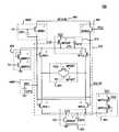
- FIG. 4is a diagram of a circuit 400 in isolation during a precharge cycle of a sense amplifier.
- the circuit 400in one embodiment, is illustrative of the sense amplifier 200 of FIG. 2 .
- the circuit 400illustrates the elements of the circuit during a precharge cycle, in accordance with one embodiment of the present invention.
- the circuit 400comprises a cross-coupled inverter latch 410 that is coupled to a reference voltage sampler circuit 440 A and 440 B, a bitline controller circuit 491 , and precharge pulling circuits 420 and 430 .
- circuit 400discloses using metal oxide semiconductor field effect transistors (MOSFETS), other embodiments are well suited to using other forms of transistors to achieve a circuit capable of sampling and holding a reference voltage as is disclosed in the present invention.
- MOSFETSmetal oxide semiconductor field effect transistors
- the cross-coupled inverter latch 410comprises p-channel metal oxide semiconductor field effect transistors (PMOS) MPL 1 412 and MPL 2 411 , and n-channel metal oxide semiconductor field effect transistors (NMOS) MNL 1 416 and MNL 2 418 .
- the transistors MPL 1 412 , MPL 2 414 , MNL 1 416 and MNL 2 418are configured to form a latch of cross-coupled inverters.
- the bitlineis precharged to a positive precharge voltage 460 by a separate power supply (not shown).
- the precharge voltageis ideally between the values as follows: one half of the threshold voltage of an NMOS transistor used in the circuit 400 (Vtn/2), and the absolute value of one half of the threshold voltage of a PMOS transistor used in the circuit 400 subtracted from the supply voltage (Vcc- ⁇
- the precharge voltage 460is the latch metastable point where the voltages REF 414 and DOUTB 412 are equal, in one embodiment when the cross-coupled inverter latch 410 is on. Ultimately, the precharge voltage 460 on the bitline is dependent on the transistor threshold voltage, supply voltage Vcc 437 , and the ratio of the pullup/pulldown transistors in the cross-coupled inverter latch 410 .
- the precharge pulling circuits 420 and 430are used for achieving a stable state in the cross-coupled inverter latch during a precharging cycle in which the reference voltage is sampled.
- the precharge pulling circuit 420comprises two NMOSs, MNPC 1 421 and MNPC 2 423 .
- the precharge pulling circuit 430comprises two PMOSs, MPPC 1 431 and MPPC 2 433 .
- the precharge pulling circuit 420 and the precharge pulling circuit 430are used to prevent current leakage from the cross-coupled inverter latch circuit 410 by shutting off the transistors in the latch circuit 410 .
- a precharge signal PC 442is pulled high.
- the inverse of the precharge signal PC 442is PC bar signal 444 , which is low.
- a second precharge signal PC 2 465is also pulled high.
- the precharge signals PC 442 and PC 2 465are pulled to the supply voltage Vcc 437 .
- the transistors MNPC 1 421 and MNPC 2 423 in the precharge pulling circuit 420turn on and effectively pull the voltage at the latch pull up (LPU) node 425 to just above ground, about one threshold voltage of an NMOS transistor above ground.
- the LPU node 425goes low with a voltage near ground, the PMOS transistors MPL 1 412 and MPL 2 411 are shut off. As such, the top portion of the cross-coupled inverter latch 410 is shut off.
- the transistors MPPC 1 431 and MPPC 2 433 in the precharge pulling circuit 430turn on and effectively pull the voltage at the latch pull down (LPU) node 435 up to a level just below the supply voltage Vcc 437 , about one threshold voltage of a PMOS transistor below the supply voltage Vcc 437 .
- the LPD node 435goes high to a voltage near Vcc, the NMOS transistors MNL 1 416 and MNL 2 418 are shut off. As such, the lower portion of the cross-coupled inverter latch 410 is shut off.
- the present embodimentemploys a shorting circuit 450 to ensure that the voltages REF 414 at node 417 and DOUTB 412 at node 413 are precharged to the same level.
- a shortis created between the node 413 representing the voltage DOUTB 412 and the node 417 representing the voltage REF 414 through the shorting circuit 450 .
- the transistors employed in the shorting circuit 450are needed only to ensure that the voltages REF 414 and DOUTB 412 are equal during the precharge cycle.
- the cross-coupled inverter latch 410is in a stable state.
- the shorting circuit 450may be comprised only of either an NMOS transistor, PMOS transistor, or a combination of both the NMOS and PMOS transistors. For example, for higher supply voltages Vcc 437 around three volts, only an NMOS transistor is only needed. For lower supply voltages Vcc 437 around 1.8 volts, a PMOS transistor is only needed.
- the configuration of the shorting circuit 450includes both an NMOS transistor MNSRT 452 and a PMOS transistor MPSRT 454 to account for both high and low supply voltages Vcc 437 .
- the NMOS transistor MNIN 1 447acts as a pass gate and turns on to pass the precharge voltage 460 from the bitline to the cross-coupled inverter latch circuit 410 .
- the NMOS transistor MNIN 2 495in the bitline controller circuit 491 , acts as a pass gate and turns on to pass the precharge voltage 460 from the bitline to the cross-coupled inverter latch 410 .
- the NMOS transistor MNIN 1 447also sets the reference voltage 414 that is sampled by the reference voltage sampler circuit 440 A and 440 B, after the precharge cycle. During the precharge cycle, a voltage on the node 417 rises to the reference voltage 414 . When the precharge signal PC 442 goes from high to low after the precharge cycle, the NMOS MNIN 1 447 turns off which sets the reference voltage 414 at the node 417 .
- the reference voltage 414is held at node 417 and can be sampled.
- the reference voltage 414is equal to the precharge voltage 460 on the bitline less a threshold voltage Vt from the NMOS MNIN 1 447 .
- the capacitors CAP 1 490 and CAP 3 493are optional capacitive elements that can be added to establish the correct voltage level for the reference voltage REF 414 seen at nod 417 .
- the present embodimentpulls the PC signal 442 low to ground.
- the PC 2 signal 465still remains high. This allows for coupling between the capacitive elements from the gate to source capacitance of MNIN 1 447 and the CAP 1490 . This coupling generates a voltage difference between the bitline 460 and the REF 414 at node 417 .
- the transistors in the precharge pulling circuit 420 and 430are turned off.
- the transistors in the shorting circuit 450are also turned off.
- the node 413 representing the voltage DOUTB 412is not directly tied to the node 417 representing the reference voltage REF 414 .
- the reference voltage REF 414will be lower than the DOUTB voltage and can be set for sampling.
- the voltage on the bitlineis allowed to reach its steady state. This is accomplished by disabling the precharge current source (not shown) that precharges the voltage on the bitline 460 to its precharge voltage level. As such, the steady state voltage on the bitline 460 will remain high if the memory cell associated with the bitline 460 is programmed. Correspondingly, the DOUTB voltage will remain high, so that the voltage DOUTB 412 is higher than the reference voltage 414 .
- the voltage on the bitline 460will discharge until reaching a steady state. As such, the voltage on the bitline 460 will remain low in its steady state when the memory cell associated with the bitline 460 is erased. As a result, the DOUTB voltage 412 will go low so that the voltage DOUTB 412 is lower than the reference voltage 414 .
- FIG. 5illustrates a voltage versus time chart illustrating the bitline voltage as seen on the bitline during a precharge cycle, a cycle in which the bitline voltage reaches a static state, and a sensing cycle.
- the curve 510represents the voltage on the bitline associated with a memory cell from which its state is being determined.
- the curve 510rises up to the precharge voltage at point A.
- the dotted line 520represents the reference voltage as sampled from the precharge voltage determined at point A.
- the bitlineAfter the bitline is precharged to the precharge voltage at point A, the bitline is allowed to reach its steady state. At point B, the curve 510 forks into two paths 510 A and 510 B.
- the voltage on the bitline when in a steady stateremains the same (logic level 1) and is greater than the reference voltage represented by dotted line 520 .
- the voltage on the bitlinedissipates to a low level (logic level 0) when in its steady state and is smaller in magnitude than the reference voltage represented by dotted line 520 .
- ⁇ V 520represents the difference in voltages when the memory cell is programmed
- ⁇ V 530represents the difference in voltages when the memory cell is erased. Amplification of ⁇ V 520 and ⁇ V 530 occurs in the cross-coupled inverter latch circuit 410 during the sensing cycle.
- FIG. 6is a circuit diagram illustrating a sensing circuit 600 in isolation of a sense amplifier during a sensing cycle, in accordance with one embodiment of the present invention.
- the circuit 400in one embodiment, is illustrative of the sense amplifier 200 of FIG. 2 .
- the sensing circuit 600is capable of holding a reference voltage and amplifying a difference in a static bitline voltage and the reference voltage.
- the sensing circuit 600is used in combination with the circuit 400 to form a sense amplifier that is capable of sampling and holding a reference voltage from a precharge voltage on a bitline for use to determine the state of a memory cell associated with the sampled bitline.
- the sensing circuit 600comprises the cross-coupled inverter latch 410 , the reference voltage sampler circuits 440 A and 440 B, and the bitline controller circuit 460 , as disclosed in FIG. 4 .
- the sensing circuit 600comprises a pull up circuit 610 and a pull down circuit 620 for enabling the transistors in the cross-coupled inverter latch 410 .
- the present embodimentenables the sensing circuit by pulling the PC signal 442 low and pulling the charge share (CS) signal 630 high. This occurs by after the cycle that allows the voltage on the bitline to reach a steady state.
- the PC signal 442goes low in the circuit 400 of FIG. 4, the transistors in the precharge pulling circuits 420 and 430 turn off. This allows the voltage on the bitline to reach a steady state.
- the pull up circuit 610 and pull down circuit 620can be enabled in FIG. 6 by asserting the CS signal 630 during the sensing cycle.
- the pull up circuit 610 and pull down circuit 620are enabled without any influence from the precharge pulling circuit 420 and 430 .
- the CS signal 630is pulled high to the supply voltage Vcc 437 .
- the CS bar signal 635goes low to ground (0).
- the CS signal 630is pulled high after a sufficient amount of time has passed to ensure that the voltage at DOUTB 412 can discharge to a level lower than the reference voltage REF 414 .
- the pull up circuit 610pulls the LPU node 425 up to the supply voltage Vcc 437 during the sensing cycle.
- the PMOS transistor MPSUP 615 in the pull up circuit 610is enabled and pulls the LPU node 425 up to the supply voltage Vcc 437 .
- the top portion of the cross-coupled inverter latch 410comprising the PMOS transistors MPL 1 412 and MPL 2 414 , is enabled.
- the CS signal 630was low (0) and the CS bar signal 635 was high.
- the PMOS transistor MPSUP 615was turned off, thereby disabling the pull up circuit 610 .
- MPSUP 615static power dissipation through the pull up circuit 610 is avoided.
- the pull down circuit 620pulls the LPD node 435 down to ground (0), during the sensing cycle.
- the NMOS transistor MNSUP 625 in the pull down circuit 620is enabled and pulls the LPD node 435 down to ground.
- the lower portion of the cross-coupled inverter latch 410comprising the NMOS transistors MNL 1 4166 and MNL 2 418 , is enabled.
- the CS signal 630was low (0).
- the NMOS transistor MNSUP 625was turned off, thereby disabling the pull down circuit 620 .
- MNSUP 625static power dissipation through the pull down circuit 620 is avoided.
- the pull up circuit 610also comprises a capacitor CAP 2 617 coupled to the PMOS transistor 615 .
- the pull down circuit 620also comprises a capacitor CAP 4 627 .
- the capacitors CAP 2 617 and CAP 4 627are optional filtering capacitors to reduce noise signals on the LPU node 425 and the LPD node 435 so that the DOUTB voltage 412 at node 413 and the REF voltage at node 417 are more stable.
- the CAP 2 617 and CAP 4 627 capacitorsare used so that the LPD node 435 and the LPU node 425 do not couple high and low, respectively.
- the parasitic capacitances associated with the PMOS transistors MPSUP 615 , MPL 1 412 , and the MPL 2 414may be sufficient to preclude the use of the optional CAP 2 617 capacitor.
- the parasitic capacitances associated with the NMOS transistors MNSUP 625 , MNL 1 416 , and MNL 2 418may be sufficient to preclude the use of the optional CAP 4 627 capacitor.
- the cross-coupled inverter latch 410When the pull up circuit 610 and the pull down circuit 620 are enabled, the cross-coupled inverter latch 410 also becomes enabled thereby amplifying the difference between the steady state voltage on the bitline and the reference voltage 414 . Once a sufficient amount of time has elapsed to ensure that the voltage DOUTB 412 could discharge below the reference voltage 414 , the CS 630 signal toggles high. Shortly after the CS signal 630 and the CS bar signal 635 toggle high and low, respectively, the PC 2 signal 465 can be pulled low. This turns off the path to the bitline 460 after the cross-coupled latch has started to flip the voltages DOUTB 412 at node 413 and REF 414 at node 417 to the full Vcc 437 level or to ground.
- the cross-coupled inverter latch 410functions to swing the greater of the voltage DOUTB 412 at node 413 and reference voltage REF 414 at node 417 to the supply voltage Vcc 437 .
- the cross-coupled inverter latch 410functions to swing the lesser of the voltage DOUTB 412 at node 413 and the reference voltage REF 414 at node 417 to ground.
- the voltage DOUTB 412 seen at node 413will either be high at Vcc 437 or low at ground.
- the voltage DOUTB 412will be greater than the reference voltage REF 414 .
- the cross-coupled inverter latchwill swing the voltage DOUTB 412 at node 413 to Vcc 437 and the voltage REF 414 at node 417 to ground.
- the voltage DOUTB 412will be less than the reference voltage REF 414 .
- the cross-coupled inverter latchwill swing the voltage DOUTB 412 to ground, and the voltage REF 414 at node 417 to Vcc 437 .
- the inverter latch 410flips the voltages DOUTB 412 and REF 414 to ground or to Vcc 437 , the inverter latch 410 has reached a stable state.
- the two possible stable states when the voltage DOUTB at node 413 and the voltage REF at node 417 are not equalare as follows: the reference voltage REF 414 at node 417 is 0, and the voltage DOUTB 412 at node 413 is Vcc 437 ; or the reference voltage REF 414 at node 417 is Vcc 437 , and the voltage DOUTB 412 at node 413 is 0.
- the stable stateno further power is consumed by the sensing circuit 600 as described in FIG. 6 .
- FIG. 7is a sensing circuit 700 that is a combination of circuit 400 and circuit 600 , in accordance with one embodiment of the present invention.
- the sensing circuit 700is capable of sampling and holding a reference voltage based on a precharge voltage of a bitline associated with a memory cell that is being read.
- the sensing circuit 700comprises the following circuit elements, in part: a cross-coupled inverter latch 410 that is coupled to a reference voltage sampler circuit 440 A and 440 B, a bitline controller circuit 491 , precharge pulling circuits 420 and 430 , shorting circuit 450 , pull up circuit 610 , and a pull down circuit 620 .
- the particular functions of the sensing circuit 700 corresponding to the circuit elements of the sensing circuit 700have been previously discussed in relation to the circuits 400 and, 600 .
- FIG. 8is a signal diagram 800 illustrating the signal patterns appearing in the circuits 400 , 600 , and 700 , in accordance with one embodiment of the present invention.
- the signal diagram 800is broken into three cycles, a precharge cycle, a cycle in which a voltage on a bitline that is associated with a memory cell that is being read, and a sensing cycle.
- Signal patterns shownrelate to the PC signal 442 , the PC 2 signal 465 , the CS signal 630 , the voltage at DOUTB 412 for a programmed memory cell, the voltage at DOUTB 412 for an erased memory cell, the voltage at the LPU node 425 , and the voltage at the LPD node 435 .
- the PC signal 442starts high during the precharge cycle to allow the cross-coupled inverter latch to reach a stable state in which the voltage DOUTB 412 and the reference voltage 414 are equalized. From this state, a reference voltage can be sampled. After the precharge cycle, the PC signal 442 goes low to allow the voltage on the bitline 460 to reach a steady state. Thereafter, the PC signal 442 remains low.
- the voltage on the bitlinewill either remain high or discharge to ground (low).
- the memory celldoes not sink any current, and the voltage on the bitline will remain high in its steady state. Similarly, the voltage DOUTB 412 will remain high.
- the memory cellsinks current, and the voltage on the bitline will discharge low in its steady state. Similarly, the voltage DOUTB 412 will go low.
- the CS signal 630is shown as starting low through the precharge cycle and the cycle allowing the voltage on the bitline to reach a steady state. After a sufficient amount of time has elapsed to ensure that the voltage DOUTB 412 could discharge lower than the reference voltage REF 414 , then the CS signal 630 is toggled high to enable the cross-coupled inverter latch 410 .
- the PC 2 signal 465also starts high during the precharge cycle to pass the voltage from the bitline 460 down to the cross-coupled inverter latch 410 .
- PC 2 signal 465is brought low in the present embodiment to turn off the bitline path back to the bitline 460 after the cross-coupled inverter latch 410 has started to flip the voltages seen on its outputs.
- the pull up circuit 610is enabled, and the voltage at the LPU node 425 also goes high.
- the pull down circuit 620is enabled when the CS signal is toggled high, and the voltage at the LPD node 435 goes low.
- FIG. 9is a flow chart 900 illustrating steps in a computer implemented method for sampling and holding a reference voltage in a sensing circuit, in accordance with one embodiment of the present invention.
- the present embodimentbegins by sampling a reference voltage based on a precharge voltage of a bitline during a precharge cycle, in step 910 . Previously, the bitline was precharged to the precharge voltage.
- the reference voltageis equal to a precharge voltage from the bitline. Normally, there is no voltage drop between the precharge voltage and the reference voltage. However, there will be a threshold drop across the pass gate of the pass transistor (e.g., gate of MNIN 1 447 ) when the voltage on the pass gate is less than or equal to the precharge voltage of the bitline plus a threshold voltage. In that case, the threshold voltage is the precharge voltage less the threshold voltage. In either case, the present embodiment is able to avoid the costly process of generating a reference voltage by using the existing precharge voltage on the bitline associated with a memory cell being read.
- the present embodimentdisables a cross-coupled inverter latch during the precharge cycle.
- the cross-coupled inverter latchis coupled to the bitline associated with the memory cell being read. More specifically, the cross-coupled inverter latch is disabled by reaching a stable state during the precharging cycle. In the stable state, the reference voltage is equal to a precharged output voltage of the cross-coupled inverter latch. The precharged voltage is based on a precharged voltage from the bitline.
- the present embodimentpulls down a latch pull up (LPU) node in the cross-coupled inverter latch to disable an upper first inverter amplifier comprising the cross-coupled inverter latch.
- the present embodimentpulls up a latch pull down (LPD) node in the cross-coupled inverter latch. This is done to disable a lower second inverter amplifier comprising the cross-coupled inverter latch.
- LPUlatch pull up
- LPDlatch pull down
- the present embodimentholds the reference voltage after the precharge cycle.
- the reference voltageis used to determine the state of the memory cell associated with the bitline.
- the reference voltageis held using capacitive elements in the sensing circuit.
- the present embodimentamplifies a voltage difference between an output voltage of the cross-coupled inverter latch and the reference voltage.
- the present embodimentaccomplishes this by enabling the cross-coupled inverter latch after the precharge cycle.
- the output voltageis based on the static bitline voltage from the bitline.
- the voltage on the bitlinereaches a steady slate to achieve the static bitline voltage.
- the present embodimentamplifies the voltage difference between the output voltage and the reference voltage by pulling the greater of the output voltage and the reference voltage to a high voltage (e.g., the supply voltage). In addition, the present embodiment pulls the lesser of the output voltage and said reference voltage through said cross-coupled inverter latch to a low level to amplify the voltage difference between the output voltage and the reference voltage.
- a high voltagee.g., the supply voltage
- the present embodimentpulls the lesser of the output voltage and said reference voltage through said cross-coupled inverter latch to a low level to amplify the voltage difference between the output voltage and the reference voltage.
- the capacitor CAP 1 490is replaced with a weak pull up path to the bitline.
- the voltage on the bitlinewill charge up high if the data on the memory cell indicates it is in a programmed state (0).
- the reference voltageis effectively the precharge level, and the bitline either charges higher or discharges lower.
- a weak pullup in currentthat is matched to the maximum allowable leakage current can be added to the bitline. This cancels out the leakage current. As long as this weak pullup current provides less current than is apparent from a memory cell that is in an erased state, then the reference voltage is effectively the precharge level, and the bitline either charges higher or discharges lower.
Landscapes
- Read Only Memory (AREA)
Abstract
Description
Claims (26)
Priority Applications (1)
| Application Number | Priority Date | Filing Date | Title |
|---|---|---|---|
| US10/389,149US6819612B1 (en) | 2003-03-13 | 2003-03-13 | Apparatus and method for a sense amplifier circuit that samples and holds a reference voltage |
Applications Claiming Priority (1)
| Application Number | Priority Date | Filing Date | Title |
|---|---|---|---|
| US10/389,149US6819612B1 (en) | 2003-03-13 | 2003-03-13 | Apparatus and method for a sense amplifier circuit that samples and holds a reference voltage |
Publications (1)
| Publication Number | Publication Date |
|---|---|
| US6819612B1true US6819612B1 (en) | 2004-11-16 |
Family
ID=33415764
Family Applications (1)
| Application Number | Title | Priority Date | Filing Date |
|---|---|---|---|
| US10/389,149Expired - LifetimeUS6819612B1 (en) | 2003-03-13 | 2003-03-13 | Apparatus and method for a sense amplifier circuit that samples and holds a reference voltage |
Country Status (1)
| Country | Link |
|---|---|
| US (1) | US6819612B1 (en) |
Cited By (164)
| Publication number | Priority date | Publication date | Assignee | Title |
|---|---|---|---|---|
| US20030223298A1 (en)* | 2002-02-28 | 2003-12-04 | Stmicroelectronics Pvt. Ltd. | Efficient latch array initialization |
| US20060195276A1 (en)* | 2002-09-19 | 2006-08-31 | Marvell International Ltd. Argyle House | Configurable voltage regulator |
| US20060250871A1 (en)* | 2004-09-01 | 2006-11-09 | Micron Technology, Inc. | Sample and hold memory sense amplifier |
| US20060262621A1 (en)* | 2004-08-31 | 2006-11-23 | Micron Technology, Inc. | Switched capacitor DRAM sense amplifier with immunity to mismatch and offsets |
| US20060274587A1 (en)* | 2005-06-02 | 2006-12-07 | Texas Instruments Inc. | Static random-access memory having reduced bit line precharge voltage and method of operating the same |
| US20070043988A1 (en)* | 2002-09-19 | 2007-02-22 | Sehat Sutardja | Configurable voltage regulator |
| US20080049495A1 (en)* | 2006-08-28 | 2008-02-28 | Shigekazu Yamada | Method, apparatus and system relating to automatic cell threshold voltage measurement |
| US20090116290A1 (en)* | 2006-08-25 | 2009-05-07 | Micron Technology, Inc. | Methods and apparatuses relating to automatic cell threshold voltage measurement |
| US20100125429A1 (en)* | 2008-11-14 | 2010-05-20 | Micron Technology, Inc. | Automatic word line leakage measurement circuitry |
| US20110305063A1 (en)* | 2010-06-10 | 2011-12-15 | Hewlett-Packard Development Company, L.P. | Sense amplifier for reading a crossbar memory array |
| US20120182818A1 (en)* | 2011-01-14 | 2012-07-19 | Taiwan Semiconductor Manufacturing Co., Ltd. | Low power and high speed sense amplifier |
| US8542549B2 (en)* | 2011-08-08 | 2013-09-24 | Taiwan Semiconductor Manufacturing Company, Ltd. | Electrical fuse bit cell |
| US8576649B1 (en)* | 2010-07-02 | 2013-11-05 | Farid Nemati | Sense amplifiers and operations thereof |
| US8588007B2 (en) | 2011-02-28 | 2013-11-19 | Micron Technology, Inc. | Leakage measurement systems |
| US8634264B2 (en) | 2011-10-26 | 2014-01-21 | Micron Technology, Inc. | Apparatuses, integrated circuits, and methods for measuring leakage current |
| US8942026B2 (en) | 2010-11-19 | 2015-01-27 | Hewlett-Packard Development Company, L.P. | Circuit and method for reading a resistive switching device in an array |
| US20150042380A1 (en)* | 2013-08-08 | 2015-02-12 | Micron Technology, Inc. | Apparatuses and methods for performing logical operations using sensing circuitry |
| US9158667B2 (en) | 2013-03-04 | 2015-10-13 | Micron Technology, Inc. | Apparatuses and methods for performing logical operations using sensing circuitry |
| US20150340087A1 (en)* | 2013-03-22 | 2015-11-26 | Masahiro Takahashi | Nonvolatile random access memory |
| US9275725B2 (en)* | 2013-05-03 | 2016-03-01 | Samsung Electronics Co., Ltd. | Memory device and method of operating the same |
| US9430191B2 (en) | 2013-11-08 | 2016-08-30 | Micron Technology, Inc. | Division operations for memory |
| US9437256B2 (en) | 2013-09-19 | 2016-09-06 | Micron Technology, Inc. | Data shifting |
| US9449675B2 (en) | 2013-10-31 | 2016-09-20 | Micron Technology, Inc. | Apparatuses and methods for identifying an extremum value stored in an array of memory cells |
| US9449674B2 (en) | 2014-06-05 | 2016-09-20 | Micron Technology, Inc. | Performing logical operations using sensing circuitry |
| US9455020B2 (en) | 2014-06-05 | 2016-09-27 | Micron Technology, Inc. | Apparatuses and methods for performing an exclusive or operation using sensing circuitry |
| US9466340B2 (en) | 2013-07-26 | 2016-10-11 | Micron Technology, Inc. | Apparatuses and methods for performing compare operations using sensing circuitry |
| US9496023B2 (en) | 2014-06-05 | 2016-11-15 | Micron Technology, Inc. | Comparison operations on logical representations of values in memory |
| US9530475B2 (en) | 2013-08-30 | 2016-12-27 | Micron Technology, Inc. | Independently addressable memory array address spaces |
| US9583163B2 (en) | 2015-02-03 | 2017-02-28 | Micron Technology, Inc. | Loop structure for operations in memory |
| US9589602B2 (en) | 2014-09-03 | 2017-03-07 | Micron Technology, Inc. | Comparison operations in memory |
| US9659610B1 (en) | 2016-05-18 | 2017-05-23 | Micron Technology, Inc. | Apparatuses and methods for shifting data |
| US9659605B1 (en) | 2016-04-20 | 2017-05-23 | Micron Technology, Inc. | Apparatuses and methods for performing corner turn operations using sensing circuitry |
| US9672930B2 (en) | 2015-05-29 | 2017-06-06 | Silicon Storage Technology, Inc. | Low power operation for flash memory system |
| US9697876B1 (en) | 2016-03-01 | 2017-07-04 | Micron Technology, Inc. | Vertical bit vector shift in memory |
| US9704540B2 (en) | 2014-06-05 | 2017-07-11 | Micron Technology, Inc. | Apparatuses and methods for parity determination using sensing circuitry |
| US9704541B2 (en) | 2015-06-12 | 2017-07-11 | Micron Technology, Inc. | Simulating access lines |
| US9711206B2 (en) | 2014-06-05 | 2017-07-18 | Micron Technology, Inc. | Performing logical operations using sensing circuitry |
| US9711207B2 (en) | 2014-06-05 | 2017-07-18 | Micron Technology, Inc. | Performing logical operations using sensing circuitry |
| US9740607B2 (en) | 2014-09-03 | 2017-08-22 | Micron Technology, Inc. | Swap operations in memory |
| US9741399B2 (en) | 2015-03-11 | 2017-08-22 | Micron Technology, Inc. | Data shift by elements of a vector in memory |
| US9747961B2 (en) | 2014-09-03 | 2017-08-29 | Micron Technology, Inc. | Division operations in memory |
| US9747960B2 (en) | 2014-12-01 | 2017-08-29 | Micron Technology, Inc. | Apparatuses and methods for converting a mask to an index |
| US9761300B1 (en) | 2016-11-22 | 2017-09-12 | Micron Technology, Inc. | Data shift apparatuses and methods |
| US9767892B1 (en) | 2016-04-27 | 2017-09-19 | Altera Corporation | Memory elements with dynamic pull-up weakening write assist circuitry |
| US9767864B1 (en) | 2016-07-21 | 2017-09-19 | Micron Technology, Inc. | Apparatuses and methods for storing a data value in a sensing circuitry element |
| US9779019B2 (en) | 2014-06-05 | 2017-10-03 | Micron Technology, Inc. | Data storage layout |
| US9779784B2 (en) | 2014-10-29 | 2017-10-03 | Micron Technology, Inc. | Apparatuses and methods for performing logical operations using sensing circuitry |
| US9786335B2 (en) | 2014-06-05 | 2017-10-10 | Micron Technology, Inc. | Apparatuses and methods for performing logical operations using sensing circuitry |
| US9805772B1 (en) | 2016-10-20 | 2017-10-31 | Micron Technology, Inc. | Apparatuses and methods to selectively perform logical operations |
| US9818459B2 (en) | 2016-04-19 | 2017-11-14 | Micron Technology, Inc. | Invert operations using sensing circuitry |
| US9830999B2 (en) | 2014-06-05 | 2017-11-28 | Micron Technology, Inc. | Comparison operations in memory |
| US9836218B2 (en) | 2014-10-03 | 2017-12-05 | Micron Technology, Inc. | Computing reduction and prefix sum operations in memory |
| US9847110B2 (en) | 2014-09-03 | 2017-12-19 | Micron Technology, Inc. | Apparatuses and methods for storing a data value in multiple columns of an array corresponding to digits of a vector |
| US9892767B2 (en) | 2016-02-12 | 2018-02-13 | Micron Technology, Inc. | Data gathering in memory |
| US9898252B2 (en) | 2014-09-03 | 2018-02-20 | Micron Technology, Inc. | Multiplication operations in memory |
| US9898253B2 (en) | 2015-03-11 | 2018-02-20 | Micron Technology, Inc. | Division operations on variable length elements in memory |
| US9899070B2 (en) | 2016-02-19 | 2018-02-20 | Micron Technology, Inc. | Modified decode for corner turn |
| US9904515B2 (en) | 2014-09-03 | 2018-02-27 | Micron Technology, Inc. | Multiplication operations in memory |
| US9905276B2 (en) | 2015-12-21 | 2018-02-27 | Micron Technology, Inc. | Control of sensing components in association with performing operations |
| US9910637B2 (en) | 2016-03-17 | 2018-03-06 | Micron Technology, Inc. | Signed division in memory |
| US9910787B2 (en) | 2014-06-05 | 2018-03-06 | Micron Technology, Inc. | Virtual address table |
| US9921777B2 (en) | 2015-06-22 | 2018-03-20 | Micron Technology, Inc. | Apparatuses and methods for data transfer from sensing circuitry to a controller |
| US9934856B2 (en) | 2014-03-31 | 2018-04-03 | Micron Technology, Inc. | Apparatuses and methods for comparing data patterns in memory |
| US9940026B2 (en) | 2014-10-03 | 2018-04-10 | Micron Technology, Inc. | Multidimensional contiguous memory allocation |
| US9952925B2 (en) | 2016-01-06 | 2018-04-24 | Micron Technology, Inc. | Error code calculation on sensing circuitry |
| US9959923B2 (en) | 2015-04-16 | 2018-05-01 | Micron Technology, Inc. | Apparatuses and methods to reverse data stored in memory |
| US9971541B2 (en) | 2016-02-17 | 2018-05-15 | Micron Technology, Inc. | Apparatuses and methods for data movement |
| US9972367B2 (en) | 2016-07-21 | 2018-05-15 | Micron Technology, Inc. | Shifting data in sensing circuitry |
| US9990181B2 (en) | 2016-08-03 | 2018-06-05 | Micron Technology, Inc. | Apparatuses and methods for random number generation |
| US9997232B2 (en) | 2016-03-10 | 2018-06-12 | Micron Technology, Inc. | Processing in memory (PIM) capable memory device having sensing circuitry performing logic operations |
| US9996479B2 (en) | 2015-08-17 | 2018-06-12 | Micron Technology, Inc. | Encryption of executables in computational memory |
| US9997212B1 (en) | 2017-04-24 | 2018-06-12 | Micron Technology, Inc. | Accessing data in memory |
| US10014034B2 (en) | 2016-10-06 | 2018-07-03 | Micron Technology, Inc. | Shifting data in sensing circuitry |
| US10013197B1 (en) | 2017-06-01 | 2018-07-03 | Micron Technology, Inc. | Shift skip |
| US10032493B2 (en) | 2015-01-07 | 2018-07-24 | Micron Technology, Inc. | Longest element length determination in memory |
| US10037785B2 (en) | 2016-07-08 | 2018-07-31 | Micron Technology, Inc. | Scan chain operation in sensing circuitry |
| US10042608B2 (en) | 2016-05-11 | 2018-08-07 | Micron Technology, Inc. | Signed division in memory |
| US10043570B1 (en) | 2017-04-17 | 2018-08-07 | Micron Technology, Inc. | Signed element compare in memory |
| US10049721B1 (en) | 2017-03-27 | 2018-08-14 | Micron Technology, Inc. | Apparatuses and methods for in-memory operations |
| US10048888B2 (en) | 2016-02-10 | 2018-08-14 | Micron Technology, Inc. | Apparatuses and methods for partitioned parallel data movement |
| US10049054B2 (en) | 2015-04-01 | 2018-08-14 | Micron Technology, Inc. | Virtual register file |
| US10049707B2 (en) | 2016-06-03 | 2018-08-14 | Micron Technology, Inc. | Shifting data |
| US10061590B2 (en) | 2015-01-07 | 2018-08-28 | Micron Technology, Inc. | Generating and executing a control flow |
| US10068652B2 (en) | 2014-09-03 | 2018-09-04 | Micron Technology, Inc. | Apparatuses and methods for determining population count |
| US10068664B1 (en) | 2017-05-19 | 2018-09-04 | Micron Technology, Inc. | Column repair in memory |
| US10073635B2 (en) | 2014-12-01 | 2018-09-11 | Micron Technology, Inc. | Multiple endianness compatibility |
| US10074407B2 (en) | 2014-06-05 | 2018-09-11 | Micron Technology, Inc. | Apparatuses and methods for performing invert operations using sensing circuitry |
| US10074416B2 (en) | 2016-03-28 | 2018-09-11 | Micron Technology, Inc. | Apparatuses and methods for data movement |
| US10073786B2 (en) | 2015-05-28 | 2018-09-11 | Micron Technology, Inc. | Apparatuses and methods for compute enabled cache |
| US10120740B2 (en) | 2016-03-22 | 2018-11-06 | Micron Technology, Inc. | Apparatus and methods for debugging on a memory device |
| US10140104B2 (en) | 2015-04-14 | 2018-11-27 | Micron Technology, Inc. | Target architecture determination |
| US10147480B2 (en) | 2014-10-24 | 2018-12-04 | Micron Technology, Inc. | Sort operation in memory |
| US10146537B2 (en) | 2015-03-13 | 2018-12-04 | Micron Technology, Inc. | Vector population count determination in memory |
| US10147467B2 (en) | 2017-04-17 | 2018-12-04 | Micron Technology, Inc. | Element value comparison in memory |
| US10153008B2 (en) | 2016-04-20 | 2018-12-11 | Micron Technology, Inc. | Apparatuses and methods for performing corner turn operations using sensing circuitry |
| US10152271B1 (en) | 2017-06-07 | 2018-12-11 | Micron Technology, Inc. | Data replication |
| US10163467B2 (en) | 2014-10-16 | 2018-12-25 | Micron Technology, Inc. | Multiple endianness compatibility |
| US10162005B1 (en) | 2017-08-09 | 2018-12-25 | Micron Technology, Inc. | Scan chain operations |
| US10185674B2 (en) | 2017-03-22 | 2019-01-22 | Micron Technology, Inc. | Apparatus and methods for in data path compute operations |
| US10199088B2 (en) | 2016-03-10 | 2019-02-05 | Micron Technology, Inc. | Apparatuses and methods for cache invalidate |
| US10236038B2 (en) | 2017-05-15 | 2019-03-19 | Micron Technology, Inc. | Bank to bank data transfer |
| US10262701B2 (en) | 2017-06-07 | 2019-04-16 | Micron Technology, Inc. | Data transfer between subarrays in memory |
| US10268389B2 (en) | 2017-02-22 | 2019-04-23 | Micron Technology, Inc. | Apparatuses and methods for in-memory operations |
| US10289542B2 (en) | 2015-02-06 | 2019-05-14 | Micron Technology, Inc. | Apparatuses and methods for memory device as a store for block program instructions |
| US10303632B2 (en) | 2016-07-26 | 2019-05-28 | Micron Technology, Inc. | Accessing status information |
| US10318168B2 (en) | 2017-06-19 | 2019-06-11 | Micron Technology, Inc. | Apparatuses and methods for simultaneous in data path compute operations |
| US10332586B1 (en) | 2017-12-19 | 2019-06-25 | Micron Technology, Inc. | Apparatuses and methods for subrow addressing |
| US10346092B2 (en) | 2017-08-31 | 2019-07-09 | Micron Technology, Inc. | Apparatuses and methods for in-memory operations using timing circuitry |
| US10365851B2 (en) | 2015-03-12 | 2019-07-30 | Micron Technology, Inc. | Apparatuses and methods for data movement |
| US10373666B2 (en) | 2016-11-08 | 2019-08-06 | Micron Technology, Inc. | Apparatuses and methods for compute components formed over an array of memory cells |
| US10379772B2 (en) | 2016-03-16 | 2019-08-13 | Micron Technology, Inc. | Apparatuses and methods for operations using compressed and decompressed data |
| US10388360B2 (en) | 2016-07-19 | 2019-08-20 | Micron Technology, Inc. | Utilization of data stored in an edge section of an array |
| US10387046B2 (en) | 2016-06-22 | 2019-08-20 | Micron Technology, Inc. | Bank to bank data transfer |
| US10387058B2 (en) | 2016-09-29 | 2019-08-20 | Micron Technology, Inc. | Apparatuses and methods to change data category values |
| US10388393B2 (en) | 2016-03-22 | 2019-08-20 | Micron Technology, Inc. | Apparatus and methods for debugging on a host and memory device |
| US10387299B2 (en) | 2016-07-20 | 2019-08-20 | Micron Technology, Inc. | Apparatuses and methods for transferring data |
| US10403352B2 (en) | 2017-02-22 | 2019-09-03 | Micron Technology, Inc. | Apparatuses and methods for compute in data path |
| US10402340B2 (en) | 2017-02-21 | 2019-09-03 | Micron Technology, Inc. | Memory array page table walk |
| US10409739B2 (en) | 2017-10-24 | 2019-09-10 | Micron Technology, Inc. | Command selection policy |
| US10416927B2 (en) | 2017-08-31 | 2019-09-17 | Micron Technology, Inc. | Processing in memory |
| US10423353B2 (en) | 2016-11-11 | 2019-09-24 | Micron Technology, Inc. | Apparatuses and methods for memory alignment |
| US10430244B2 (en) | 2016-03-28 | 2019-10-01 | Micron Technology, Inc. | Apparatuses and methods to determine timing of operations |
| US10440341B1 (en) | 2018-06-07 | 2019-10-08 | Micron Technology, Inc. | Image processor formed in an array of memory cells |
| US10437557B2 (en) | 2018-01-31 | 2019-10-08 | Micron Technology, Inc. | Determination of a match between data values stored by several arrays |
| US10453502B2 (en) | 2016-04-04 | 2019-10-22 | Micron Technology, Inc. | Memory bank power coordination including concurrently performing a memory operation in a selected number of memory regions |
| US10466928B2 (en) | 2016-09-15 | 2019-11-05 | Micron Technology, Inc. | Updating a register in memory |
| US10468087B2 (en) | 2016-07-28 | 2019-11-05 | Micron Technology, Inc. | Apparatuses and methods for operations in a self-refresh state |
| US10474581B2 (en) | 2016-03-25 | 2019-11-12 | Micron Technology, Inc. | Apparatuses and methods for cache operations |
| US10483978B1 (en) | 2018-10-16 | 2019-11-19 | Micron Technology, Inc. | Memory device processing |
| US10496286B2 (en) | 2015-02-06 | 2019-12-03 | Micron Technology, Inc. | Apparatuses and methods for parallel writing to multiple memory device structures |
| US10522199B2 (en) | 2015-02-06 | 2019-12-31 | Micron Technology, Inc. | Apparatuses and methods for scatter and gather |
| US10523472B1 (en)* | 2017-10-02 | 2019-12-31 | Marvell International Ltd. | Interface circuitry |
| US10522210B2 (en) | 2017-12-14 | 2019-12-31 | Micron Technology, Inc. | Apparatuses and methods for subarray addressing |
| US10522212B2 (en) | 2015-03-10 | 2019-12-31 | Micron Technology, Inc. | Apparatuses and methods for shift decisions |
| US10529409B2 (en) | 2016-10-13 | 2020-01-07 | Micron Technology, Inc. | Apparatuses and methods to perform logical operations using sensing circuitry |
| US10534553B2 (en) | 2017-08-30 | 2020-01-14 | Micron Technology, Inc. | Memory array accessibility |
| US10606587B2 (en) | 2016-08-24 | 2020-03-31 | Micron Technology, Inc. | Apparatus and methods related to microcode instructions indicating instruction types |
| US10607665B2 (en) | 2016-04-07 | 2020-03-31 | Micron Technology, Inc. | Span mask generation |
| US10614875B2 (en) | 2018-01-30 | 2020-04-07 | Micron Technology, Inc. | Logical operations using memory cells |
| US10725696B2 (en) | 2018-04-12 | 2020-07-28 | Micron Technology, Inc. | Command selection policy with read priority |
| US10733089B2 (en) | 2016-07-20 | 2020-08-04 | Micron Technology, Inc. | Apparatuses and methods for write address tracking |
| US10741239B2 (en) | 2017-08-31 | 2020-08-11 | Micron Technology, Inc. | Processing in memory device including a row address strobe manager |
| US10826268B1 (en) | 2019-06-27 | 2020-11-03 | Stmicroelectronics S.R.L. | Laser driver incorporating clamping circuit with freewheeling diode |
| US10838899B2 (en) | 2017-03-21 | 2020-11-17 | Micron Technology, Inc. | Apparatuses and methods for in-memory data switching networks |
| US20200412344A1 (en)* | 2019-06-27 | 2020-12-31 | Stmicroelectronics S.R.L. | Pvt compensated delay cell for a monostable |
| US10942843B2 (en) | 2017-04-25 | 2021-03-09 | Micron Technology, Inc. | Storing data elements of different lengths in respective adjacent rows or columns according to memory shapes |
| US10956439B2 (en) | 2016-02-19 | 2021-03-23 | Micron Technology, Inc. | Data transfer with a bit vector operation device |
| US10978111B1 (en)* | 2019-12-05 | 2021-04-13 | Winbond Electronics Corp. | Sense amplifier circuit with reference voltage holding circuit for maintaining sense amplifier reference voltage when the sense amplifier operates under standby mode |
| US10977033B2 (en) | 2016-03-25 | 2021-04-13 | Micron Technology, Inc. | Mask patterns generated in memory from seed vectors |
| US11029951B2 (en) | 2016-08-15 | 2021-06-08 | Micron Technology, Inc. | Smallest or largest value element determination |
| US11074988B2 (en) | 2016-03-22 | 2021-07-27 | Micron Technology, Inc. | Apparatus and methods for debugging on a host and memory device |
| US11175915B2 (en) | 2018-10-10 | 2021-11-16 | Micron Technology, Inc. | Vector registers implemented in memory |
| US11184446B2 (en) | 2018-12-05 | 2021-11-23 | Micron Technology, Inc. | Methods and apparatus for incentivizing participation in fog networks |
| US11194477B2 (en) | 2018-01-31 | 2021-12-07 | Micron Technology, Inc. | Determination of a match between data values stored by three or more arrays |
| CN113870911A (en)* | 2020-06-30 | 2021-12-31 | 长鑫存储技术(上海)有限公司 | Sensitive amplifier, storage device and read/write method |
| US11222260B2 (en) | 2017-03-22 | 2022-01-11 | Micron Technology, Inc. | Apparatuses and methods for operating neural networks |
| US11227641B1 (en) | 2020-07-21 | 2022-01-18 | Micron Technology, Inc. | Arithmetic operations in memory |
| US11360768B2 (en) | 2019-08-14 | 2022-06-14 | Micron Technolgy, Inc. | Bit string operations in memory |
| US11387625B2 (en) | 2019-06-27 | 2022-07-12 | Stmicroelectronics S.R.L. | Pulse width check circuit for laser diode pulse generator |
| US11398264B2 (en) | 2019-07-08 | 2022-07-26 | Micron Technology, Inc. | Methods and apparatus for dynamically adjusting performance of partitioned memory |
| US11397688B2 (en) | 2018-10-10 | 2022-07-26 | Micron Technology, Inc. | Coherent memory access |
| US11449577B2 (en) | 2019-11-20 | 2022-09-20 | Micron Technology, Inc. | Methods and apparatus for performing video processing matrix operations within a memory array |
| US11853385B2 (en) | 2019-12-05 | 2023-12-26 | Micron Technology, Inc. | Methods and apparatus for performing diversity matrix operations within a memory array |
| US12118056B2 (en) | 2019-05-03 | 2024-10-15 | Micron Technology, Inc. | Methods and apparatus for performing matrix transformations within a memory array |
Citations (3)
| Publication number | Priority date | Publication date | Assignee | Title |
|---|---|---|---|---|
| US4694205A (en)* | 1985-06-03 | 1987-09-15 | Advanced Micro Devices, Inc. | Midpoint sense amplification scheme for a CMOS DRAM |
| US6515926B1 (en)* | 2002-01-04 | 2003-02-04 | United Memories, Inc. | Shared sense amplifier driver technique for dynamic random access memories exhibiting improved write recovery time |
| US6657471B1 (en)* | 2002-11-08 | 2003-12-02 | International Business Machines Corporation | High performance, low power differential latch |
- 2003
- 2003-03-13USUS10/389,149patent/US6819612B1/ennot_activeExpired - Lifetime
Patent Citations (3)
| Publication number | Priority date | Publication date | Assignee | Title |
|---|---|---|---|---|
| US4694205A (en)* | 1985-06-03 | 1987-09-15 | Advanced Micro Devices, Inc. | Midpoint sense amplification scheme for a CMOS DRAM |
| US6515926B1 (en)* | 2002-01-04 | 2003-02-04 | United Memories, Inc. | Shared sense amplifier driver technique for dynamic random access memories exhibiting improved write recovery time |
| US6657471B1 (en)* | 2002-11-08 | 2003-12-02 | International Business Machines Corporation | High performance, low power differential latch |
Non-Patent Citations (2)
| Title |
|---|
| Christanthopoulos, A. et al, "A New Flash Memory Sense Amplifier In 0.18mum CMOS Technology," 0-7803-7057-0/01 (C)2001, IEEE. |
| Christanthopoulos, A. et al, "A New Flash Memory Sense Amplifier In 0.18μm CMOS Technology," 0-7803-7057-0/01 ©2001, IEEE. |
Cited By (474)
| Publication number | Priority date | Publication date | Assignee | Title |
|---|---|---|---|---|
| US7180792B2 (en)* | 2002-02-28 | 2007-02-20 | Stmicroelectronics Pvt. Ltd. | Efficient latch array initialization |
| US20030223298A1 (en)* | 2002-02-28 | 2003-12-04 | Stmicroelectronics Pvt. Ltd. | Efficient latch array initialization |
| US20070043988A1 (en)* | 2002-09-19 | 2007-02-22 | Sehat Sutardja | Configurable voltage regulator |
| US7516027B2 (en) | 2002-09-19 | 2009-04-07 | Marvell World Trade Ltd. | Configurable voltage regulator |
| US7788053B2 (en) | 2002-09-19 | 2010-08-31 | Marvell International Ltd. | Configurable voltage regulator |
| US20100321037A1 (en)* | 2002-09-19 | 2010-12-23 | Sehat Sutardja | Configurable voltage regulator |
| US7437252B2 (en) | 2002-09-19 | 2008-10-14 | Marvell International Ltd. | Configurable voltage regulator |
| US20070043987A1 (en)* | 2002-09-19 | 2007-02-22 | Sehat Sutardja | Configurable voltage regulator |
| US20070067135A1 (en)* | 2002-09-19 | 2007-03-22 | Sehat Sutardja | Configurable voltage regulator |
| US7209845B2 (en)* | 2002-09-19 | 2007-04-24 | Marvell Internation Ltd. | Configurable voltage regulator |
| US20070103351A1 (en)* | 2002-09-19 | 2007-05-10 | Sehat Sutardja | Testing system using configurable integrated circuit |
| US20070198201A1 (en)* | 2002-09-19 | 2007-08-23 | Sehat Sutardja | Configurable voltage regulator |
| US20060195276A1 (en)* | 2002-09-19 | 2006-08-31 | Marvell International Ltd. Argyle House | Configurable voltage regulator |
| US7343256B2 (en)* | 2002-09-19 | 2008-03-11 | Marvell International, Ltd. | Configurable voltage regulator |
| US7512504B2 (en) | 2002-09-19 | 2009-03-31 | Marvell World Trade Ltd. | Testing system using configurable integrated circuit |
| US7979224B2 (en) | 2002-09-19 | 2011-07-12 | Marvell International Ltd. | Configurable voltage regulator |
| US20080197860A1 (en)* | 2002-09-19 | 2008-08-21 | Sehat Sutardja | Configurable voltage regulator |
| US7480578B2 (en) | 2002-09-19 | 2009-01-20 | Marvell World Trade Ltd. | Configurable voltage regulator |
| US7443749B2 (en) | 2004-08-31 | 2008-10-28 | Micron Technology, Inc. | Switched capacitor DRAM sense amplifier with immunity to mismatch and offsets |
| US7443750B2 (en) | 2004-08-31 | 2008-10-28 | Micron Technology, Inc. | Switched capacitor DRAM sense amplifier with immunity to mismatch and offsets |
| US20090040810A1 (en)* | 2004-08-31 | 2009-02-12 | Micron Technology, Inc. | Switched capacitor dram sense amplifier with immunity to mismatch and offsets |
| US20060262621A1 (en)* | 2004-08-31 | 2006-11-23 | Micron Technology, Inc. | Switched capacitor DRAM sense amplifier with immunity to mismatch and offsets |
| US7729189B2 (en) | 2004-08-31 | 2010-06-01 | Micron Technology, Inc. | Switched capacitor DRAM sense amplifier with immunity to mismatch and offsets |
| US7453751B2 (en)* | 2004-09-01 | 2008-11-18 | Micron Technology, Inc. | Sample and hold memory sense amplifier |
| US20060250871A1 (en)* | 2004-09-01 | 2006-11-09 | Micron Technology, Inc. | Sample and hold memory sense amplifier |
| US7570527B2 (en)* | 2005-06-02 | 2009-08-04 | Texas Instruments Incorporated | Static random-access memory having reduced bit line precharge voltage and method of operating the same |
| US20060274587A1 (en)* | 2005-06-02 | 2006-12-07 | Texas Instruments Inc. | Static random-access memory having reduced bit line precharge voltage and method of operating the same |
| US7920428B2 (en) | 2006-08-25 | 2011-04-05 | Micron Technology, Inc. | Methods and apparatuses relating to automatic cell threshold voltage measurement |
| US20090116290A1 (en)* | 2006-08-25 | 2009-05-07 | Micron Technology, Inc. | Methods and apparatuses relating to automatic cell threshold voltage measurement |
| US7483305B2 (en)* | 2006-08-28 | 2009-01-27 | Micron Technology, Inc. | Method, apparatus and system relating to automatic cell threshold voltage measurement |
| US20080049495A1 (en)* | 2006-08-28 | 2008-02-28 | Shigekazu Yamada | Method, apparatus and system relating to automatic cell threshold voltage measurement |
| US20100125429A1 (en)* | 2008-11-14 | 2010-05-20 | Micron Technology, Inc. | Automatic word line leakage measurement circuitry |
| US9704542B2 (en) | 2008-11-14 | 2017-07-11 | Micron Technology, Inc. | Automatic word line leakage measurement circuitry |
| US9159452B2 (en) | 2008-11-14 | 2015-10-13 | Micron Technology, Inc. | Automatic word line leakage measurement circuitry |
| US20110305063A1 (en)* | 2010-06-10 | 2011-12-15 | Hewlett-Packard Development Company, L.P. | Sense amplifier for reading a crossbar memory array |
| US8472262B2 (en)* | 2010-06-10 | 2013-06-25 | Hewlett-Packard Development Company, L.P. | Sense amplifier for reading a crossbar memory array |
| US8576649B1 (en)* | 2010-07-02 | 2013-11-05 | Farid Nemati | Sense amplifiers and operations thereof |
| US8942026B2 (en) | 2010-11-19 | 2015-01-27 | Hewlett-Packard Development Company, L.P. | Circuit and method for reading a resistive switching device in an array |
| US20120182818A1 (en)* | 2011-01-14 | 2012-07-19 | Taiwan Semiconductor Manufacturing Co., Ltd. | Low power and high speed sense amplifier |
| US8339884B2 (en)* | 2011-01-14 | 2012-12-25 | Taiwan Semiconductor Manufacturing Company, Inc. | Low power and high speed sense amplifier |
| US8947946B2 (en) | 2011-02-28 | 2015-02-03 | Micron Technology, Inc. | Leakage measurement systems |
| US8588007B2 (en) | 2011-02-28 | 2013-11-19 | Micron Technology, Inc. | Leakage measurement systems |
| US9269410B2 (en) | 2011-02-28 | 2016-02-23 | Micron Technology, Inc. | Leakage measurement systems |
| US8542549B2 (en)* | 2011-08-08 | 2013-09-24 | Taiwan Semiconductor Manufacturing Company, Ltd. | Electrical fuse bit cell |
| US9183948B2 (en) | 2011-10-26 | 2015-11-10 | Micron Technology, Inc. | Apparatuses, integrated circuits, and methods for measuring leakage current |
| US8867290B2 (en) | 2011-10-26 | 2014-10-21 | Micron Technology, Inc. | Apparatuses, integrated circuits, and methods for measuring leakage current |
| US8634264B2 (en) | 2011-10-26 | 2014-01-21 | Micron Technology, Inc. | Apparatuses, integrated circuits, and methods for measuring leakage current |
| US9892766B2 (en) | 2013-03-04 | 2018-02-13 | Micron Technology, Inc. | Apparatuses and methods for performing logical operations using sensing circuitry |
| US11727963B2 (en) | 2013-03-04 | 2023-08-15 | Micron Technology, Inc. | Apparatuses and methods for performing logical operations using sensing circuitry |
| US9158667B2 (en) | 2013-03-04 | 2015-10-13 | Micron Technology, Inc. | Apparatuses and methods for performing logical operations using sensing circuitry |
| US9959913B2 (en) | 2013-03-04 | 2018-05-01 | Micron Technology, Inc. | Apparatuses and methods for performing logical operations using sensing circuitry |
| US9472265B2 (en) | 2013-03-04 | 2016-10-18 | Micron Technology, Inc. | Apparatuses and methods for performing logical operations using sensing circuitry |
| US10431264B2 (en) | 2013-03-04 | 2019-10-01 | Micron Technology, Inc. | Apparatuses and methods for performing logical operations using sensing circuitry |
| US10796733B2 (en) | 2013-03-04 | 2020-10-06 | Micron Technology, Inc. | Apparatuses and methods for performing logical operations using sensing circuitry |
| US11276439B2 (en) | 2013-03-04 | 2022-03-15 | Micron Technology, Inc. | Apparatuses and methods for performing logical operations using sensing circuitry |
| US10153009B2 (en) | 2013-03-04 | 2018-12-11 | Micron Technology, Inc. | Apparatuses and methods for performing logical operations using sensing circuitry |
| US20150340087A1 (en)* | 2013-03-22 | 2015-11-26 | Masahiro Takahashi | Nonvolatile random access memory |
| US9336871B2 (en)* | 2013-03-22 | 2016-05-10 | Masahiro Takahashi | Resistance change memory |
| US9275725B2 (en)* | 2013-05-03 | 2016-03-01 | Samsung Electronics Co., Ltd. | Memory device and method of operating the same |
| US10056122B2 (en) | 2013-07-26 | 2018-08-21 | Micron Technology, Inc. | Apparatuses and methods for performing compare operations using sensing circuitry |
| US9799378B2 (en) | 2013-07-26 | 2017-10-24 | Micron Technology, Inc. | Apparatuses and methods for performing compare operations using sensing circuitry |
| US10643673B2 (en) | 2013-07-26 | 2020-05-05 | Micron Technology, Inc. | Apparatuses and methods for performing compare operations using sensing circuitry |
| US9466340B2 (en) | 2013-07-26 | 2016-10-11 | Micron Technology, Inc. | Apparatuses and methods for performing compare operations using sensing circuitry |
| US9589607B2 (en) | 2013-08-08 | 2017-03-07 | Micron Technology, Inc. | Apparatuses and methods for performing logical operations using sensing circuitry |
| US20150042380A1 (en)* | 2013-08-08 | 2015-02-12 | Micron Technology, Inc. | Apparatuses and methods for performing logical operations using sensing circuitry |
| US9899068B2 (en) | 2013-08-08 | 2018-02-20 | Micron Technology, Inc. | Apparatuses and methods for performing logical operations using sensing circuitry |
| US10878863B2 (en) | 2013-08-08 | 2020-12-29 | Micron Technology, Inc. | Apparatuses and methods for performing logical operations using sensing circuitry |
| US8971124B1 (en)* | 2013-08-08 | 2015-03-03 | Micron Technology, Inc. | Apparatuses and methods for performing logical operations using sensing circuitry |
| US11495274B2 (en) | 2013-08-08 | 2022-11-08 | Micron Technology, Inc. | Apparatuses and methods for performing logical operations using sensing circuitry |
| US10535384B2 (en) | 2013-08-08 | 2020-01-14 | Micron Technology, Inc. | Apparatuses and methods for performing logical operations using sensing circuitry |
| US10186303B2 (en) | 2013-08-08 | 2019-01-22 | Micron Technology, Inc. | Apparatuses and methods for performing logical operations using sensing circuitry |
| US12142347B2 (en) | 2013-08-08 | 2024-11-12 | Lodestar Licensing Group Llc | Apparatuses and methods for performing logical operations using sensing circuitry |
| US9275701B2 (en) | 2013-08-08 | 2016-03-01 | Micron Technology, Inc. | Apparatuses and methods for performing logical operations using sensing circuitry |
| US9530475B2 (en) | 2013-08-30 | 2016-12-27 | Micron Technology, Inc. | Independently addressable memory array address spaces |
| US9437256B2 (en) | 2013-09-19 | 2016-09-06 | Micron Technology, Inc. | Data shifting |
| US9830955B2 (en) | 2013-09-19 | 2017-11-28 | Micron Technology, Inc. | Data shifting |
| US10043556B2 (en) | 2013-09-19 | 2018-08-07 | Micron Technology, Inc. | Data shifting |
| US9449675B2 (en) | 2013-10-31 | 2016-09-20 | Micron Technology, Inc. | Apparatuses and methods for identifying an extremum value stored in an array of memory cells |
| US9430191B2 (en) | 2013-11-08 | 2016-08-30 | Micron Technology, Inc. | Division operations for memory |
| US10579336B2 (en) | 2013-11-08 | 2020-03-03 | Micron Technology, Inc. | Division operations for memory |
| US10055196B2 (en) | 2013-11-08 | 2018-08-21 | Micron Technology, Inc. | Division operations for memory |
| US9934856B2 (en) | 2014-03-31 | 2018-04-03 | Micron Technology, Inc. | Apparatuses and methods for comparing data patterns in memory |
| US10726919B2 (en) | 2014-03-31 | 2020-07-28 | Micron Technology, Inc. | Apparatuses and methods for comparing data patterns in memory |
| US11393531B2 (en) | 2014-03-31 | 2022-07-19 | Micron Technology, Inc. | Apparatuses and methods for comparing data patterns in memory |
| US10360147B2 (en) | 2014-06-05 | 2019-07-23 | Micron Technology, Inc. | Data storage layout |
| US9711206B2 (en) | 2014-06-05 | 2017-07-18 | Micron Technology, Inc. | Performing logical operations using sensing circuitry |
| US9449674B2 (en) | 2014-06-05 | 2016-09-20 | Micron Technology, Inc. | Performing logical operations using sensing circuitry |
| US10210911B2 (en) | 2014-06-05 | 2019-02-19 | Micron Technology, Inc. | Apparatuses and methods for performing logical operations using sensing circuitry in a memory device |
| US11967361B2 (en) | 2014-06-05 | 2024-04-23 | Micron Technology, Inc. | Comparison operations in memory |
| US9455020B2 (en) | 2014-06-05 | 2016-09-27 | Micron Technology, Inc. | Apparatuses and methods for performing an exclusive or operation using sensing circuitry |
| US9830999B2 (en) | 2014-06-05 | 2017-11-28 | Micron Technology, Inc. | Comparison operations in memory |
| US9779019B2 (en) | 2014-06-05 | 2017-10-03 | Micron Technology, Inc. | Data storage layout |
| US10249350B2 (en) | 2014-06-05 | 2019-04-02 | Micron Technology, Inc. | Apparatuses and methods for parity determination using sensing circuitry |
| US11120850B2 (en) | 2014-06-05 | 2021-09-14 | Micron Technology, Inc. | Performing logical operations using sensing circuitry |
| US11205497B2 (en) | 2014-06-05 | 2021-12-21 | Micron Technology, Inc. | Comparison operations in memory |
| US10255193B2 (en) | 2014-06-05 | 2019-04-09 | Micron Technology, Inc. | Virtual address table |
| US10290344B2 (en) | 2014-06-05 | 2019-05-14 | Micron Technology, Inc. | Performing logical operations using sensing circuitry |
| US10304519B2 (en) | 2014-06-05 | 2019-05-28 | Micron Technology, Inc. | Apparatuses and methods for performing an exclusive or operation using sensing circuitry |
| US11238920B2 (en) | 2014-06-05 | 2022-02-01 | Micron Technology, Inc. | Comparison operations in memory |
| US10424350B2 (en) | 2014-06-05 | 2019-09-24 | Micron Technology, Inc. | Performing logical operations using sensing circuitry |
| US10090041B2 (en) | 2014-06-05 | 2018-10-02 | Micro Technology, Inc. | Performing logical operations using sensing circuitry |
| US9496023B2 (en) | 2014-06-05 | 2016-11-15 | Micron Technology, Inc. | Comparison operations on logical representations of values in memory |
| US10074407B2 (en) | 2014-06-05 | 2018-09-11 | Micron Technology, Inc. | Apparatuses and methods for performing invert operations using sensing circuitry |
| US12437801B2 (en) | 2014-06-05 | 2025-10-07 | Lodestar Licensing Group Llc | Comparison operations in memory |
| US9910787B2 (en) | 2014-06-05 | 2018-03-06 | Micron Technology, Inc. | Virtual address table |
| US10839867B2 (en) | 2014-06-05 | 2020-11-17 | Micron Technology, Inc. | Apparatuses and methods for parity determination using sensing circuitry |
| US10839892B2 (en) | 2014-06-05 | 2020-11-17 | Micron Technology, Inc. | Comparison operations in memory |
| US10453499B2 (en) | 2014-06-05 | 2019-10-22 | Micron Technology, Inc. | Apparatuses and methods for performing an in-place inversion using sensing circuitry |
| US10490257B2 (en) | 2014-06-05 | 2019-11-26 | Micron Technology, Inc. | Comparison operations in memory |
| US10593418B2 (en) | 2014-06-05 | 2020-03-17 | Micron Technology, Inc. | Comparison operations in memory |
| US11355178B2 (en) | 2014-06-05 | 2022-06-07 | Micron Technology, Inc. | Apparatuses and methods for performing an exclusive or operation using sensing circuitry |
| US10522211B2 (en) | 2014-06-05 | 2019-12-31 | Micron Technology, Inc. | Performing logical operations using sensing circuitry |
| US9786335B2 (en) | 2014-06-05 | 2017-10-10 | Micron Technology, Inc. | Apparatuses and methods for performing logical operations using sensing circuitry |
| US11422933B2 (en) | 2014-06-05 | 2022-08-23 | Micron Technology, Inc. | Data storage layout |
| US9704540B2 (en) | 2014-06-05 | 2017-07-11 | Micron Technology, Inc. | Apparatuses and methods for parity determination using sensing circuitry |
| US9741427B2 (en) | 2014-06-05 | 2017-08-22 | Micron Technology, Inc. | Performing logical operations using sensing circuitry |
| US10754787B2 (en) | 2014-06-05 | 2020-08-25 | Micron Technology, Inc. | Virtual address table |
| US9711207B2 (en) | 2014-06-05 | 2017-07-18 | Micron Technology, Inc. | Performing logical operations using sensing circuitry |
| US10381065B2 (en) | 2014-06-05 | 2019-08-13 | Micron Technology, Inc. | Performing logical operations using sensing circuitry |
| US10734038B2 (en) | 2014-06-05 | 2020-08-04 | Micron Technology, Inc. | Apparatuses and methods for performing logical operations using sensing circuitry |
| US10032491B2 (en) | 2014-09-03 | 2018-07-24 | Micron Technology, Inc. | Apparatuses and methods for storing a data value in multiple columns |
| US9847110B2 (en) | 2014-09-03 | 2017-12-19 | Micron Technology, Inc. | Apparatuses and methods for storing a data value in multiple columns of an array corresponding to digits of a vector |
| US10705798B2 (en) | 2014-09-03 | 2020-07-07 | Micron Technology, Inc. | Multiplication operations in memory |
| US9779789B2 (en) | 2014-09-03 | 2017-10-03 | Micron Technology, Inc. | Comparison operations in memory |
| US9740607B2 (en) | 2014-09-03 | 2017-08-22 | Micron Technology, Inc. | Swap operations in memory |
| US10157126B2 (en) | 2014-09-03 | 2018-12-18 | Micron Technology, Inc. | Swap operations in memory |
| US10713011B2 (en) | 2014-09-03 | 2020-07-14 | Micron Technology, Inc. | Multiplication operations in memory |
| US10409555B2 (en) | 2014-09-03 | 2019-09-10 | Micron Technology, Inc. | Multiplication operations in memory |
| US9898252B2 (en) | 2014-09-03 | 2018-02-20 | Micron Technology, Inc. | Multiplication operations in memory |
| US10559360B2 (en) | 2014-09-03 | 2020-02-11 | Micron Technology, Inc. | Apparatuses and methods for determining population count |
| US9940985B2 (en) | 2014-09-03 | 2018-04-10 | Micron Technology, Inc. | Comparison operations in memory |
| US9904515B2 (en) | 2014-09-03 | 2018-02-27 | Micron Technology, Inc. | Multiplication operations in memory |
| US9940981B2 (en) | 2014-09-03 | 2018-04-10 | Micron Technology, Inc. | Division operations in memory |
| US10861563B2 (en) | 2014-09-03 | 2020-12-08 | Micron Technology, Inc. | Apparatuses and methods for determining population count |
| US10409554B2 (en) | 2014-09-03 | 2019-09-10 | Micron Technology, Inc. | Multiplication operations in memory |
| US10068652B2 (en) | 2014-09-03 | 2018-09-04 | Micron Technology, Inc. | Apparatuses and methods for determining population count |
| US9589602B2 (en) | 2014-09-03 | 2017-03-07 | Micron Technology, Inc. | Comparison operations in memory |
| US9747961B2 (en) | 2014-09-03 | 2017-08-29 | Micron Technology, Inc. | Division operations in memory |
| US11768600B2 (en) | 2014-10-03 | 2023-09-26 | Micron Technology, Inc. | Computing reduction and prefix sum operations in memory |
| US10956043B2 (en) | 2014-10-03 | 2021-03-23 | Micron Technology, Inc. | Computing reduction and prefix sum operations in memory |
| US10540093B2 (en) | 2014-10-03 | 2020-01-21 | Micron Technology, Inc. | Multidimensional contiguous memory allocation |
| US9940026B2 (en) | 2014-10-03 | 2018-04-10 | Micron Technology, Inc. | Multidimensional contiguous memory allocation |
| US9836218B2 (en) | 2014-10-03 | 2017-12-05 | Micron Technology, Inc. | Computing reduction and prefix sum operations in memory |
| US10261691B2 (en) | 2014-10-03 | 2019-04-16 | Micron Technology, Inc. | Computing reduction and prefix sum operations in memory |
| US10163467B2 (en) | 2014-10-16 | 2018-12-25 | Micron Technology, Inc. | Multiple endianness compatibility |
| US10593377B2 (en) | 2014-10-16 | 2020-03-17 | Micron Technology, Inc. | Multiple endianness compatibility |
| US10984842B2 (en) | 2014-10-16 | 2021-04-20 | Micron Technology, Inc. | Multiple endianness compatibility |
| US10685699B2 (en) | 2014-10-24 | 2020-06-16 | Micron Technology, Inc. | Sort operation in memory |
| US11315626B2 (en) | 2014-10-24 | 2022-04-26 | Micron Technology, Inc. | Sort operation in memory |
| US10147480B2 (en) | 2014-10-24 | 2018-12-04 | Micron Technology, Inc. | Sort operation in memory |
| US10529387B2 (en) | 2014-10-29 | 2020-01-07 | Micron Technology, Inc. | Apparatuses and methods for performing logical operations using sensing circuitry |
| US10074406B2 (en) | 2014-10-29 | 2018-09-11 | Micron Technology, Inc. | Apparatuses and methods for performing logical operations using sensing circuitry |
| US9779784B2 (en) | 2014-10-29 | 2017-10-03 | Micron Technology, Inc. | Apparatuses and methods for performing logical operations using sensing circuitry |
| US10073635B2 (en) | 2014-12-01 | 2018-09-11 | Micron Technology, Inc. | Multiple endianness compatibility |
| US10460773B2 (en) | 2014-12-01 | 2019-10-29 | Micron Technology, Inc. | Apparatuses and methods for converting a mask to an index |
| US10983706B2 (en) | 2014-12-01 | 2021-04-20 | Micron Technology, Inc. | Multiple endianness compatibility |
| US10037786B2 (en) | 2014-12-01 | 2018-07-31 | Micron Technology, Inc. | Apparatuses and methods for converting a mask to an index |
| US10387055B2 (en) | 2014-12-01 | 2019-08-20 | Micron Technology, Inc. | Multiple endianness compatibility |
| US9747960B2 (en) | 2014-12-01 | 2017-08-29 | Micron Technology, Inc. | Apparatuses and methods for converting a mask to an index |
| US10782980B2 (en) | 2015-01-07 | 2020-09-22 | Micron Technology, Inc. | Generating and executing a control flow |
| US10032493B2 (en) | 2015-01-07 | 2018-07-24 | Micron Technology, Inc. | Longest element length determination in memory |
| US11334362B2 (en) | 2015-01-07 | 2022-05-17 | Micron Technology, Inc. | Generating and executing a control flow |
| US12223328B2 (en) | 2015-01-07 | 2025-02-11 | Lodestar Licensing Group, Llc | Generating and executing a control flow |
| US10061590B2 (en) | 2015-01-07 | 2018-08-28 | Micron Technology, Inc. | Generating and executing a control flow |
| US11726791B2 (en) | 2015-01-07 | 2023-08-15 | Micron Technology, Inc. | Generating and executing a control flow |
| US10984841B2 (en) | 2015-01-07 | 2021-04-20 | Micron Technology, Inc. | Longest element length determination in memory |
| US10593376B2 (en) | 2015-01-07 | 2020-03-17 | Micron Technology, Inc. | Longest element length determination in memory |
| US9583163B2 (en) | 2015-02-03 | 2017-02-28 | Micron Technology, Inc. | Loop structure for operations in memory |
| US10176851B2 (en) | 2015-02-03 | 2019-01-08 | Micron Technology, Inc. | Loop structure for operations in memory |
| US10964358B2 (en) | 2015-02-06 | 2021-03-30 | Micron Technology, Inc. | Apparatuses and methods for scatter and gather |
| US10522199B2 (en) | 2015-02-06 | 2019-12-31 | Micron Technology, Inc. | Apparatuses and methods for scatter and gather |
| US10817414B2 (en) | 2015-02-06 | 2020-10-27 | Micron Technology, Inc. | Apparatuses and methods for memory device as a store for block program instructions |
| US12393342B2 (en) | 2015-02-06 | 2025-08-19 | Lodestar Licensing Group Llc | Apparatuses and methods for parallel writing to multiple memory device structures |
| US12230354B2 (en) | 2015-02-06 | 2025-02-18 | Lodestar Licensing Group Llc | Apparatuses and methods for scatter and gather |
| US11681440B2 (en) | 2015-02-06 | 2023-06-20 | Micron Technology, Inc. | Apparatuses and methods for parallel writing to multiple memory device structures |
| US10289542B2 (en) | 2015-02-06 | 2019-05-14 | Micron Technology, Inc. | Apparatuses and methods for memory device as a store for block program instructions |
| US10496286B2 (en) | 2015-02-06 | 2019-12-03 | Micron Technology, Inc. | Apparatuses and methods for parallel writing to multiple memory device structures |
| US10942652B2 (en) | 2015-02-06 | 2021-03-09 | Micron Technology, Inc. | Apparatuses and methods for parallel writing to multiple memory device structures |
| US11263123B2 (en) | 2015-02-06 | 2022-03-01 | Micron Technology, Inc. | Apparatuses and methods for memory device as a store for program instructions |
| US11482260B2 (en) | 2015-02-06 | 2022-10-25 | Micron Technology, Inc. | Apparatuses and methods for scatter and gather |
| US11107520B2 (en) | 2015-03-10 | 2021-08-31 | Micron Technology, Inc. | Apparatuses and methods for shift decisions |
| US10522212B2 (en) | 2015-03-10 | 2019-12-31 | Micron Technology, Inc. | Apparatuses and methods for shift decisions |
| US9898253B2 (en) | 2015-03-11 | 2018-02-20 | Micron Technology, Inc. | Division operations on variable length elements in memory |
| US9928887B2 (en) | 2015-03-11 | 2018-03-27 | Micron Technology, Inc. | Data shift by elements of a vector in memory |
| US9741399B2 (en) | 2015-03-11 | 2017-08-22 | Micron Technology, Inc. | Data shift by elements of a vector in memory |
| US10365851B2 (en) | 2015-03-12 | 2019-07-30 | Micron Technology, Inc. | Apparatuses and methods for data movement |
| US10936235B2 (en) | 2015-03-12 | 2021-03-02 | Micron Technology, Inc. | Apparatuses and methods for data movement |
| US11614877B2 (en) | 2015-03-12 | 2023-03-28 | Micron Technology, Inc. | Apparatuses and methods for data movement |
| US12242848B2 (en) | 2015-03-13 | 2025-03-04 | Lodestar Licensing Group Llc | Vector population count determination via comparison iterations in memory |
| US10896042B2 (en) | 2015-03-13 | 2021-01-19 | Micron Technology, Inc. | Vector population count determination via comparison iterations in memory |
| US10146537B2 (en) | 2015-03-13 | 2018-12-04 | Micron Technology, Inc. | Vector population count determination in memory |
| US11663005B2 (en) | 2015-03-13 | 2023-05-30 | Micron Technology, Inc. | Vector population count determination via comparsion iterations in memory |
| US10049054B2 (en) | 2015-04-01 | 2018-08-14 | Micron Technology, Inc. | Virtual register file |
| US10963398B2 (en) | 2015-04-01 | 2021-03-30 | Micron Technology, Inc. | Virtual register file |
| US11237808B2 (en) | 2015-04-14 | 2022-02-01 | Micron Technology, Inc. | Target architecture determination |
| US11782688B2 (en) | 2015-04-14 | 2023-10-10 | Micron Technology, Inc. | Target architecture determination |
| US10140104B2 (en) | 2015-04-14 | 2018-11-27 | Micron Technology, Inc. | Target architecture determination |
| US10795653B2 (en) | 2015-04-14 | 2020-10-06 | Micron Technology, Inc. | Target architecture determination |
| US9959923B2 (en) | 2015-04-16 | 2018-05-01 | Micron Technology, Inc. | Apparatuses and methods to reverse data stored in memory |
| US10878884B2 (en) | 2015-04-16 | 2020-12-29 | Micron Technology, Inc. | Apparatuses and methods to reverse data stored in memory |
| US10418092B2 (en) | 2015-04-16 | 2019-09-17 | Micron Technology, Inc. | Apparatuses and methods to reverse data stored in memory |
| US11599475B2 (en) | 2015-05-28 | 2023-03-07 | Micron Technology, Inc. | Apparatuses and methods for compute enabled cache |
| US10970218B2 (en) | 2015-05-28 | 2021-04-06 | Micron Technology, Inc. | Apparatuses and methods for compute enabled cache |
| US10372612B2 (en) | 2015-05-28 | 2019-08-06 | Micron Technology, Inc. | Apparatuses and methods for compute enabled cache |
| US12050536B2 (en) | 2015-05-28 | 2024-07-30 | Lodestar Licensing Group Llc | Apparatuses and methods for compute enabled cache |
| US10073786B2 (en) | 2015-05-28 | 2018-09-11 | Micron Technology, Inc. | Apparatuses and methods for compute enabled cache |
| US10141062B2 (en)* | 2015-05-29 | 2018-11-27 | Silicon Storage Technology, Inc. | Sensing circuit with sampled reference current or voltage for flash memory system |
| US9672930B2 (en) | 2015-05-29 | 2017-06-06 | Silicon Storage Technology, Inc. | Low power operation for flash memory system |
| US9990966B2 (en) | 2015-06-12 | 2018-06-05 | Micron Technology, Inc. | Simulating access lines |
| US10431263B2 (en) | 2015-06-12 | 2019-10-01 | Micron Technology, Inc. | Simulating access lines |
| US9704541B2 (en) | 2015-06-12 | 2017-07-11 | Micron Technology, Inc. | Simulating access lines |
| US11106389B2 (en) | 2015-06-22 | 2021-08-31 | Micron Technology, Inc. | Apparatuses and methods for data transfer from sensing circuitry to a controller |
| US10157019B2 (en) | 2015-06-22 | 2018-12-18 | Micron Technology, Inc. | Apparatuses and methods for data transfer from sensing circuitry to a controller |
| US9921777B2 (en) | 2015-06-22 | 2018-03-20 | Micron Technology, Inc. | Apparatuses and methods for data transfer from sensing circuitry to a controller |
| US9996479B2 (en) | 2015-08-17 | 2018-06-12 | Micron Technology, Inc. | Encryption of executables in computational memory |
| US11625336B2 (en) | 2015-08-17 | 2023-04-11 | Micron Technology, Inc. | Encryption of executables in computational memory |
| US10691620B2 (en) | 2015-08-17 | 2020-06-23 | Micron Technology, Inc. | Encryption of executables in computational memory |
| US9905276B2 (en) | 2015-12-21 | 2018-02-27 | Micron Technology, Inc. | Control of sensing components in association with performing operations |
| US10236037B2 (en) | 2015-12-21 | 2019-03-19 | Micron Technology, Inc. | Data transfer in sensing components |
| US10152374B2 (en) | 2016-01-06 | 2018-12-11 | Micron Technology, Inc. | Error code calculation on sensing circuitry |
| US9952925B2 (en) | 2016-01-06 | 2018-04-24 | Micron Technology, Inc. | Error code calculation on sensing circuitry |
| US11593200B2 (en) | 2016-01-06 | 2023-02-28 | Micron Technology, Inc. | Error code calculation on sensing circuitry |
| US10423486B2 (en) | 2016-01-06 | 2019-09-24 | Micron Technology, Inc. | Error code calculation on sensing circuitry |
| US10949299B2 (en) | 2016-01-06 | 2021-03-16 | Micron Technology, Inc. | Error code calculation on sensing circuitry |
| US11340983B2 (en) | 2016-01-06 | 2022-05-24 | Micron Technology, Inc. | Error code calculation on sensing circuitry |
| US10915263B2 (en) | 2016-02-10 | 2021-02-09 | Micron Technology, Inc. | Apparatuses and methods for partitioned parallel data movement |
| US10324654B2 (en) | 2016-02-10 | 2019-06-18 | Micron Technology, Inc. | Apparatuses and methods for partitioned parallel data movement |
| US10048888B2 (en) | 2016-02-10 | 2018-08-14 | Micron Technology, Inc. | Apparatuses and methods for partitioned parallel data movement |
| US11513713B2 (en) | 2016-02-10 | 2022-11-29 | Micron Technology, Inc. | Apparatuses and methods for partitioned parallel data movement |
| US10026459B2 (en) | 2016-02-12 | 2018-07-17 | Micron Technology, Inc. | Data gathering in memory |
| US9892767B2 (en) | 2016-02-12 | 2018-02-13 | Micron Technology, Inc. | Data gathering in memory |
| US9971541B2 (en) | 2016-02-17 | 2018-05-15 | Micron Technology, Inc. | Apparatuses and methods for data movement |
| US11010085B2 (en) | 2016-02-17 | 2021-05-18 | Micron Technology, Inc. | Apparatuses and methods for data movement |
| US11614878B2 (en) | 2016-02-17 | 2023-03-28 | Micron Technology, Inc. | Apparatuses and methods for data movement |
| US10353618B2 (en) | 2016-02-17 | 2019-07-16 | Micron Technology, Inc. | Apparatuses and methods for data movement |
| US12019895B2 (en) | 2016-02-17 | 2024-06-25 | Lodestar Licensing Group Llc | Apparatuses and methods for data movement |
| US10217499B2 (en) | 2016-02-19 | 2019-02-26 | Micron Technology, Inc. | Modified decode for corner turn |
| US9899070B2 (en) | 2016-02-19 | 2018-02-20 | Micron Technology, Inc. | Modified decode for corner turn |
| US12259903B2 (en) | 2016-02-19 | 2025-03-25 | Lodestar Licensing Group Llc | Data transfer with a bit vector operation device |
| US10956439B2 (en) | 2016-02-19 | 2021-03-23 | Micron Technology, Inc. | Data transfer with a bit vector operation device |
| US10783942B2 (en) | 2016-02-19 | 2020-09-22 | Micron Technology, Inc. | Modified decode for corner turn |
| US11816123B2 (en) | 2016-02-19 | 2023-11-14 | Micron Technology, Inc. | Data transfer with a bit vector operation device |
| US9947376B2 (en) | 2016-03-01 | 2018-04-17 | Micron Technology, Inc. | Vertical bit vector shift in memory |
| US9697876B1 (en) | 2016-03-01 | 2017-07-04 | Micron Technology, Inc. | Vertical bit vector shift in memory |
| US11915741B2 (en) | 2016-03-10 | 2024-02-27 | Lodestar Licensing Group Llc | Apparatuses and methods for logic/memory devices |
| US10559347B2 (en) | 2016-03-10 | 2020-02-11 | Micron Technology, Inc. | Processing in memory (PIM) capable memory device having timing circuitry to control timing of operations |
| US9997232B2 (en) | 2016-03-10 | 2018-06-12 | Micron Technology, Inc. | Processing in memory (PIM) capable memory device having sensing circuitry performing logic operations |
| US11594274B2 (en) | 2016-03-10 | 2023-02-28 | Micron Technology, Inc. | Processing in memory (PIM)capable memory device having timing circuity to control timing of operations |
| US10878883B2 (en) | 2016-03-10 | 2020-12-29 | Micron Technology, Inc. | Apparatuses and methods for cache invalidate |
| US10902906B2 (en) | 2016-03-10 | 2021-01-26 | Micron Technology, Inc. | Apparatuses and methods for logic/memory devices |
| US10199088B2 (en) | 2016-03-10 | 2019-02-05 | Micron Technology, Inc. | Apparatuses and methods for cache invalidate |
| US10262721B2 (en) | 2016-03-10 | 2019-04-16 | Micron Technology, Inc. | Apparatuses and methods for cache invalidate |
| US11314429B2 (en) | 2016-03-16 | 2022-04-26 | Micron Technology, Inc. | Apparatuses and methods for operations using compressed and decompressed data |
| US10379772B2 (en) | 2016-03-16 | 2019-08-13 | Micron Technology, Inc. | Apparatuses and methods for operations using compressed and decompressed data |
| US9910637B2 (en) | 2016-03-17 | 2018-03-06 | Micron Technology, Inc. | Signed division in memory |
| US10409557B2 (en) | 2016-03-17 | 2019-09-10 | Micron Technology, Inc. | Signed division in memory |
| US10817360B2 (en) | 2016-03-22 | 2020-10-27 | Micron Technology, Inc. | Apparatus and methods for debugging on a memory device |
| US10120740B2 (en) | 2016-03-22 | 2018-11-06 | Micron Technology, Inc. | Apparatus and methods for debugging on a memory device |
| US10388393B2 (en) | 2016-03-22 | 2019-08-20 | Micron Technology, Inc. | Apparatus and methods for debugging on a host and memory device |
| US11074988B2 (en) | 2016-03-22 | 2021-07-27 | Micron Technology, Inc. | Apparatus and methods for debugging on a host and memory device |
| US11126557B2 (en) | 2016-03-25 | 2021-09-21 | Micron Technology, Inc. | Apparatuses and methods for cache operations |
| US11775296B2 (en) | 2016-03-25 | 2023-10-03 | Micron Technology, Inc. | Mask patterns generated in memory from seed vectors |
| US10474581B2 (en) | 2016-03-25 | 2019-11-12 | Micron Technology, Inc. | Apparatuses and methods for cache operations |
| US11693783B2 (en) | 2016-03-25 | 2023-07-04 | Micron Technology, Inc. | Apparatuses and methods for cache operations |
| US10977033B2 (en) | 2016-03-25 | 2021-04-13 | Micron Technology, Inc. | Mask patterns generated in memory from seed vectors |
| US10482948B2 (en) | 2016-03-28 | 2019-11-19 | Micron Technology, Inc. | Apparatuses and methods for data movement |
| US11016811B2 (en) | 2016-03-28 | 2021-05-25 | Micron Technology, Inc. | Apparatuses and methods to determine timing of operations |
| US10430244B2 (en) | 2016-03-28 | 2019-10-01 | Micron Technology, Inc. | Apparatuses and methods to determine timing of operations |
| US10698734B2 (en) | 2016-03-28 | 2020-06-30 | Micron Technology, Inc. | Apparatuses and methods to determine timing of operations |
| US10074416B2 (en) | 2016-03-28 | 2018-09-11 | Micron Technology, Inc. | Apparatuses and methods for data movement |
| US10453502B2 (en) | 2016-04-04 | 2019-10-22 | Micron Technology, Inc. | Memory bank power coordination including concurrently performing a memory operation in a selected number of memory regions |
| US11107510B2 (en) | 2016-04-04 | 2021-08-31 | Micron Technology, Inc. | Memory bank power coordination including concurrently performing a memory operation in a selected number of memory regions |
| US11557326B2 (en) | 2016-04-04 | 2023-01-17 | Micron Techology, Inc. | Memory power coordination |
| US10607665B2 (en) | 2016-04-07 | 2020-03-31 | Micron Technology, Inc. | Span mask generation |
| US11437079B2 (en) | 2016-04-07 | 2022-09-06 | Micron Technology, Inc. | Span mask generation |
| US10643674B2 (en) | 2016-04-19 | 2020-05-05 | Micron Technology, Inc. | Invert operations using sensing circuitry |
| US10134453B2 (en) | 2016-04-19 | 2018-11-20 | Micron Technology, Inc. | Invert operations using sensing circuitry |
| US9818459B2 (en) | 2016-04-19 | 2017-11-14 | Micron Technology, Inc. | Invert operations using sensing circuitry |
| US9659605B1 (en) | 2016-04-20 | 2017-05-23 | Micron Technology, Inc. | Apparatuses and methods for performing corner turn operations using sensing circuitry |
| US9990967B2 (en) | 2016-04-20 | 2018-06-05 | Micron Technology, Inc. | Apparatuses and methods for performing corner turn operations using sensing circuitry |
| US10699756B2 (en) | 2016-04-20 | 2020-06-30 | Micron Technology, Inc. | Apparatuses and methods for performing corner turn operations using sensing circuitry |
| US10153008B2 (en) | 2016-04-20 | 2018-12-11 | Micron Technology, Inc. | Apparatuses and methods for performing corner turn operations using sensing circuitry |
| CN109416923B (en)* | 2016-04-27 | 2023-11-17 | 太浩研究有限公司 | Memory element with dynamic pull-up weakening write assist circuit |
| WO2017189098A1 (en)* | 2016-04-27 | 2017-11-02 | Altera Corporation | Memory elements with dynamic pull-up weakening write assist circuitry |
| US9767892B1 (en) | 2016-04-27 | 2017-09-19 | Altera Corporation | Memory elements with dynamic pull-up weakening write assist circuitry |
| CN109416923A (en)* | 2016-04-27 | 2019-03-01 | 阿尔特拉公司 | Memory element with dynamic pull-up weakening write assist circuit |
| US10540144B2 (en) | 2016-05-11 | 2020-01-21 | Micron Technology, Inc. | Signed division in memory |
| US10042608B2 (en) | 2016-05-11 | 2018-08-07 | Micron Technology, Inc. | Signed division in memory |
| US9659610B1 (en) | 2016-05-18 | 2017-05-23 | Micron Technology, Inc. | Apparatuses and methods for shifting data |
| US9899064B2 (en) | 2016-05-18 | 2018-02-20 | Micron Technology, Inc. | Apparatuses and methods for shifting data |
| US10049707B2 (en) | 2016-06-03 | 2018-08-14 | Micron Technology, Inc. | Shifting data |
| US10311922B2 (en) | 2016-06-03 | 2019-06-04 | Micron Technology, Inc. | Shifting data |
| US10658017B2 (en) | 2016-06-03 | 2020-05-19 | Micron Technology, Inc. | Shifting data |
| US11755206B2 (en) | 2016-06-22 | 2023-09-12 | Micron Technology, Inc. | Bank to bank data transfer |
| US10929023B2 (en) | 2016-06-22 | 2021-02-23 | Micron Technology, Inc. | Bank to bank data transfer |
| US10387046B2 (en) | 2016-06-22 | 2019-08-20 | Micron Technology, Inc. | Bank to bank data transfer |
| US12393341B2 (en) | 2016-06-22 | 2025-08-19 | Lodestar Licensing Group Llc | Bank to bank data transfer |
| US10037785B2 (en) | 2016-07-08 | 2018-07-31 | Micron Technology, Inc. | Scan chain operation in sensing circuitry |
| US10388334B2 (en) | 2016-07-08 | 2019-08-20 | Micron Technology, Inc. | Scan chain operation in sensing circuitry |
| US10699772B2 (en) | 2016-07-19 | 2020-06-30 | Micron Technology, Inc. | Utilization of instructions stored in an edge section of an array of memory cells |
| US11468944B2 (en) | 2016-07-19 | 2022-10-11 | Micron Technology, Inc. | Utilization of data stored in an edge section of an array |
| US10388360B2 (en) | 2016-07-19 | 2019-08-20 | Micron Technology, Inc. | Utilization of data stored in an edge section of an array |
| US10387299B2 (en) | 2016-07-20 | 2019-08-20 | Micron Technology, Inc. | Apparatuses and methods for transferring data |
| US10929283B2 (en) | 2016-07-20 | 2021-02-23 | Micron Technology, Inc. | Apparatuses and methods for transferring data |
| US10733089B2 (en) | 2016-07-20 | 2020-08-04 | Micron Technology, Inc. | Apparatuses and methods for write address tracking |
| US11513945B2 (en) | 2016-07-20 | 2022-11-29 | Micron Technology, Inc. | Apparatuses and methods for transferring data using a cache |
| US10789996B2 (en) | 2016-07-21 | 2020-09-29 | Micron Technology, Inc. | Shifting data in sensing circuitry |
| US10839870B2 (en) | 2016-07-21 | 2020-11-17 | Micron Technology, Inc. | Apparatuses and methods for storing a data value in a sensing circuitry element |
| US9972367B2 (en) | 2016-07-21 | 2018-05-15 | Micron Technology, Inc. | Shifting data in sensing circuitry |
| US10242722B2 (en) | 2016-07-21 | 2019-03-26 | Micron Technology, Inc. | Shifting data in sensing circuitry |
| US9767864B1 (en) | 2016-07-21 | 2017-09-19 | Micron Technology, Inc. | Apparatuses and methods for storing a data value in a sensing circuitry element |
| US10360949B2 (en) | 2016-07-21 | 2019-07-23 | Micron Technology, Inc. | Apparatuses and methods for storing a data value in a sensing circuitry element |
| US9966116B2 (en) | 2016-07-21 | 2018-05-08 | Micron Technology, Inc. | Apparatuses and methods for storing a data value in a sensing circuitry element |
| US10725952B2 (en) | 2016-07-26 | 2020-07-28 | Micron Technology, Inc. | Accessing status information |
| US10303632B2 (en) | 2016-07-26 | 2019-05-28 | Micron Technology, Inc. | Accessing status information |
| US12165691B2 (en) | 2016-07-28 | 2024-12-10 | Lodestar Licensing Group Llc | Apparatuses and methods for operations in a self-refresh state |
| US10468087B2 (en) | 2016-07-28 | 2019-11-05 | Micron Technology, Inc. | Apparatuses and methods for operations in a self-refresh state |
| US11282563B2 (en) | 2016-07-28 | 2022-03-22 | Micron Technology, Inc. | Apparatuses and methods for operations in a self-refresh state |
| US11664064B2 (en) | 2016-07-28 | 2023-05-30 | Micron Technology, Inc. | Apparatuses and methods for operations in a self-refresh state |
| US10152304B2 (en) | 2016-08-03 | 2018-12-11 | Micron Technology, Inc. | Apparatuses and methods for random number generation |
| US10387121B2 (en) | 2016-08-03 | 2019-08-20 | Micron Technology, Inc. | Apparatuses and methods for random number generation |
| US9990181B2 (en) | 2016-08-03 | 2018-06-05 | Micron Technology, Inc. | Apparatuses and methods for random number generation |
| US11526355B2 (en) | 2016-08-15 | 2022-12-13 | Micron Technology, Inc. | Smallest or largest value element determination |
| US11029951B2 (en) | 2016-08-15 | 2021-06-08 | Micron Technology, Inc. | Smallest or largest value element determination |
| US12340217B2 (en) | 2016-08-24 | 2025-06-24 | Lodestar Licensing Group Llc | Apparatus and methods related to microcode instructions indicating instruction types |
| US11061671B2 (en) | 2016-08-24 | 2021-07-13 | Micron Technology, Inc. | Apparatus and methods related to microcode instructions indicating instruction types |
| US11842191B2 (en) | 2016-08-24 | 2023-12-12 | Micron Technology, Inc. | Apparatus and methods related to microcode instructions indicating instruction types |
| US10606587B2 (en) | 2016-08-24 | 2020-03-31 | Micron Technology, Inc. | Apparatus and methods related to microcode instructions indicating instruction types |
| US11625194B2 (en) | 2016-09-15 | 2023-04-11 | Micron Technology, Inc. | Updating a register in memory |
| US10466928B2 (en) | 2016-09-15 | 2019-11-05 | Micron Technology, Inc. | Updating a register in memory |
| US11055026B2 (en) | 2016-09-15 | 2021-07-06 | Micron Technology, Inc. | Updating a register in memory |
| US11422720B2 (en) | 2016-09-29 | 2022-08-23 | Micron Technology, Inc. | Apparatuses and methods to change data category values |
| US10725680B2 (en) | 2016-09-29 | 2020-07-28 | Micron Technology, Inc. | Apparatuses and methods to change data category values |
| US10976943B2 (en) | 2016-09-29 | 2021-04-13 | Micron Technology, Inc. | Apparatuses and methods to change data category values |
| US10387058B2 (en) | 2016-09-29 | 2019-08-20 | Micron Technology, Inc. | Apparatuses and methods to change data category values |
| US10242721B2 (en) | 2016-10-06 | 2019-03-26 | Micron Technology, Inc. | Shifting data in sensing circuitry |
| US10014034B2 (en) | 2016-10-06 | 2018-07-03 | Micron Technology, Inc. | Shifting data in sensing circuitry |
| US10600473B2 (en) | 2016-10-13 | 2020-03-24 | Micron Technology, Inc. | Apparatuses and methods to perform logical operations using sensing circuitry |
| US10529409B2 (en) | 2016-10-13 | 2020-01-07 | Micron Technology, Inc. | Apparatuses and methods to perform logical operations using sensing circuitry |
| US10971214B2 (en) | 2016-10-13 | 2021-04-06 | Micron Technology, Inc. | Apparatuses and methods to perform logical operations using sensing circuitry |
| US9805772B1 (en) | 2016-10-20 | 2017-10-31 | Micron Technology, Inc. | Apparatuses and methods to selectively perform logical operations |
| US10388333B2 (en) | 2016-10-20 | 2019-08-20 | Micron Technology, Inc. | Apparatuses and methods to selectively perform logical operations |
| US10854247B2 (en) | 2016-10-20 | 2020-12-01 | Micron Technology, Inc. | Apparatuses and methods to selectively perform logical operations |
| US11238914B2 (en) | 2016-11-08 | 2022-02-01 | Micron Technology, Inc. | Apparatuses and methods for compute components formed over an array of memory cells |
| US10373666B2 (en) | 2016-11-08 | 2019-08-06 | Micron Technology, Inc. | Apparatuses and methods for compute components formed over an array of memory cells |
| US10854269B2 (en) | 2016-11-08 | 2020-12-01 | Micron Technology, Inc. | Apparatuses and methods for compute components formed over an array of memory cells |
| US12293105B2 (en) | 2016-11-11 | 2025-05-06 | Lodestar Licensing Group Llc | Apparatuses and methods for memory alignment |
| US11693576B2 (en) | 2016-11-11 | 2023-07-04 | Micron Technology, Inc. | Apparatuses and methods for memory alignment |
| US11048428B2 (en) | 2016-11-11 | 2021-06-29 | Micron Technology, Inc. | Apparatuses and methods for memory alignment |
| US10423353B2 (en) | 2016-11-11 | 2019-09-24 | Micron Technology, Inc. | Apparatuses and methods for memory alignment |
| US9761300B1 (en) | 2016-11-22 | 2017-09-12 | Micron Technology, Inc. | Data shift apparatuses and methods |
| US9940990B1 (en) | 2016-11-22 | 2018-04-10 | Micron Technology, Inc. | Data shift apparatuses and methods |
| US12277067B2 (en) | 2017-02-21 | 2025-04-15 | Lodestar Licensing Group Llc | Memory array page table walk |
| US11663137B2 (en) | 2017-02-21 | 2023-05-30 | Micron Technology, Inc. | Memory array page table walk |
| US11182304B2 (en) | 2017-02-21 | 2021-11-23 | Micron Technology, Inc. | Memory array page table walk |
| US10402340B2 (en) | 2017-02-21 | 2019-09-03 | Micron Technology, Inc. | Memory array page table walk |
| US10540097B2 (en) | 2017-02-22 | 2020-01-21 | Micron Technology, Inc. | Apparatuses and methods for in-memory operations |
| US10268389B2 (en) | 2017-02-22 | 2019-04-23 | Micron Technology, Inc. | Apparatuses and methods for in-memory operations |
| US10403352B2 (en) | 2017-02-22 | 2019-09-03 | Micron Technology, Inc. | Apparatuses and methods for compute in data path |
| US10915249B2 (en) | 2017-02-22 | 2021-02-09 | Micron Technology, Inc. | Apparatuses and methods for in-memory operations |
| US11011220B2 (en) | 2017-02-22 | 2021-05-18 | Micron Technology, Inc. | Apparatuses and methods for compute in data path |
| US11682449B2 (en) | 2017-02-22 | 2023-06-20 | Micron Technology, Inc. | Apparatuses and methods for compute in data path |
| US11474965B2 (en) | 2017-03-21 | 2022-10-18 | Micron Technology, Inc. | Apparatuses and methods for in-memory data switching networks |
| US10838899B2 (en) | 2017-03-21 | 2020-11-17 | Micron Technology, Inc. | Apparatuses and methods for in-memory data switching networks |
| US10817442B2 (en) | 2017-03-22 | 2020-10-27 | Micron Technology, Inc. | Apparatus and methods for in data path compute operations |
| US11769053B2 (en) | 2017-03-22 | 2023-09-26 | Micron Technology, Inc. | Apparatuses and methods for operating neural networks |
| US11222260B2 (en) | 2017-03-22 | 2022-01-11 | Micron Technology, Inc. | Apparatuses and methods for operating neural networks |
| US11048652B2 (en) | 2017-03-22 | 2021-06-29 | Micron Technology, Inc. | Apparatus and methods for in data path compute operations |
| US10185674B2 (en) | 2017-03-22 | 2019-01-22 | Micron Technology, Inc. | Apparatus and methods for in data path compute operations |
| US10452578B2 (en) | 2017-03-22 | 2019-10-22 | Micron Technology, Inc. | Apparatus and methods for in data path compute operations |
| US11550742B2 (en) | 2017-03-22 | 2023-01-10 | Micron Technology, Inc. | Apparatus and methods for in data path compute operations |
| US10049721B1 (en) | 2017-03-27 | 2018-08-14 | Micron Technology, Inc. | Apparatuses and methods for in-memory operations |
| US10446221B2 (en) | 2017-03-27 | 2019-10-15 | Micron Technology, Inc. | Apparatuses and methods for in-memory operations |
| US11410717B2 (en) | 2017-03-27 | 2022-08-09 | Micron Technology, Inc. | Apparatuses and methods for in-memory operations |
| US10878885B2 (en) | 2017-03-27 | 2020-12-29 | Micron Technology, Inc. | Apparatuses and methods for in-memory operations |
| US10147467B2 (en) | 2017-04-17 | 2018-12-04 | Micron Technology, Inc. | Element value comparison in memory |
| US10622034B2 (en) | 2017-04-17 | 2020-04-14 | Micron Technology, Inc. | Element value comparison in memory |
| US10043570B1 (en) | 2017-04-17 | 2018-08-07 | Micron Technology, Inc. | Signed element compare in memory |
| US10304502B2 (en) | 2017-04-24 | 2019-05-28 | Micron Technology, Inc. | Accessing data in memory |
| US9997212B1 (en) | 2017-04-24 | 2018-06-12 | Micron Technology, Inc. | Accessing data in memory |
| US10147468B2 (en) | 2017-04-24 | 2018-12-04 | Micron Technology, Inc. | Accessing data in memory |
| US11494296B2 (en) | 2017-04-25 | 2022-11-08 | Micron Technology, Inc. | Memory shapes |
| US10942843B2 (en) | 2017-04-25 | 2021-03-09 | Micron Technology, Inc. | Storing data elements of different lengths in respective adjacent rows or columns according to memory shapes |
| US12117929B2 (en) | 2017-04-25 | 2024-10-15 | Lodestar Licensing Group Llc | Memory shapes |
| US11514957B2 (en) | 2017-05-15 | 2022-11-29 | Micron Technology, Inc. | Bank to bank data transfer |
| US12183418B2 (en) | 2017-05-15 | 2024-12-31 | Lodestar Licensing Group Llc | Bank to bank data transfer |
| US10796736B2 (en) | 2017-05-15 | 2020-10-06 | Micron Technology, Inc. | Bank to bank data transfer |
| US10236038B2 (en) | 2017-05-15 | 2019-03-19 | Micron Technology, Inc. | Bank to bank data transfer |
| US10418123B2 (en) | 2017-05-19 | 2019-09-17 | Micron Technology, Inc. | Column repair in memory |
| US10068664B1 (en) | 2017-05-19 | 2018-09-04 | Micron Technology, Inc. | Column repair in memory |
| US10496310B2 (en) | 2017-06-01 | 2019-12-03 | Micron Technology, Inc. | Shift skip |
| US10013197B1 (en) | 2017-06-01 | 2018-07-03 | Micron Technology, Inc. | Shift skip |
| US10262701B2 (en) | 2017-06-07 | 2019-04-16 | Micron Technology, Inc. | Data transfer between subarrays in memory |
| US10152271B1 (en) | 2017-06-07 | 2018-12-11 | Micron Technology, Inc. | Data replication |
| US10510381B2 (en) | 2017-06-07 | 2019-12-17 | Micron Technology, Inc. | Data transfer between subarrays in memory |
| US10776037B2 (en) | 2017-06-07 | 2020-09-15 | Micron Technology, Inc. | Data replication |
| US11526293B2 (en) | 2017-06-07 | 2022-12-13 | Micron Technology, Inc. | Data replication |
| US10878856B2 (en) | 2017-06-07 | 2020-12-29 | Micron Technology, Inc. | Data transfer between subarrays in memory |
| US10795582B2 (en) | 2017-06-19 | 2020-10-06 | Micron Technology, Inc. | Apparatuses and methods for simultaneous in data path compute operations |
| US10318168B2 (en) | 2017-06-19 | 2019-06-11 | Micron Technology, Inc. | Apparatuses and methods for simultaneous in data path compute operations |
| US11693561B2 (en) | 2017-06-19 | 2023-07-04 | Micron Technology, Inc. | Apparatuses and methods for simultaneous in data path compute operations |
| US11372550B2 (en) | 2017-06-19 | 2022-06-28 | Micron Technology, Inc. | Apparatuses and methods for simultaneous in data path compute operations |
| US10712389B2 (en) | 2017-08-09 | 2020-07-14 | Micron Technology, Inc. | Scan chain operations |
| US10162005B1 (en) | 2017-08-09 | 2018-12-25 | Micron Technology, Inc. | Scan chain operations |
| US10534553B2 (en) | 2017-08-30 | 2020-01-14 | Micron Technology, Inc. | Memory array accessibility |
| US11182085B2 (en) | 2017-08-30 | 2021-11-23 | Micron Technology, Inc. | Memory array accessibility |
| US11886715B2 (en) | 2017-08-30 | 2024-01-30 | Lodestar Licensing Group Llc | Memory array accessibility |
| US10416927B2 (en) | 2017-08-31 | 2019-09-17 | Micron Technology, Inc. | Processing in memory |
| US10741239B2 (en) | 2017-08-31 | 2020-08-11 | Micron Technology, Inc. | Processing in memory device including a row address strobe manager |
| US11586389B2 (en) | 2017-08-31 | 2023-02-21 | Micron Technology, Inc. | Processing in memory |
| US12406718B2 (en) | 2017-08-31 | 2025-09-02 | Lodestar Licensing Group Llc | Processing in memory |
| US11675538B2 (en) | 2017-08-31 | 2023-06-13 | Micron Technology, Inc. | Apparatuses and methods for in-memory operations |
| US10628085B2 (en) | 2017-08-31 | 2020-04-21 | Micron Technology, Inc. | Processing in memory |
| US10346092B2 (en) | 2017-08-31 | 2019-07-09 | Micron Technology, Inc. | Apparatuses and methods for in-memory operations using timing circuitry |
| US12159063B2 (en) | 2017-08-31 | 2024-12-03 | Lodestar Licensing Group Llc | Apparatuses and methods for in-memory operations |
| US11016706B2 (en) | 2017-08-31 | 2021-05-25 | Micron Technology, Inc. | Apparatuses for in-memory operations |
| US11894045B2 (en) | 2017-08-31 | 2024-02-06 | Lodestar Licensing Group, Llc | Processing in memory implementing VLIW controller |
| US11276457B2 (en) | 2017-08-31 | 2022-03-15 | Micron Technology, Inc. | Processing in memory |
| US11163495B2 (en) | 2017-08-31 | 2021-11-02 | Micron Technology, Inc. | Processing in memory |
| US10523472B1 (en)* | 2017-10-02 | 2019-12-31 | Marvell International Ltd. | Interface circuitry |
| US11288214B2 (en) | 2017-10-24 | 2022-03-29 | Micron Technology, Inc. | Command selection policy |
| US10409739B2 (en) | 2017-10-24 | 2019-09-10 | Micron Technology, Inc. | Command selection policy |
| US10831682B2 (en) | 2017-10-24 | 2020-11-10 | Micron Technology, Inc. | Command selection policy |
| US10522210B2 (en) | 2017-12-14 | 2019-12-31 | Micron Technology, Inc. | Apparatuses and methods for subarray addressing |
| US10867662B2 (en) | 2017-12-14 | 2020-12-15 | Micron Technology, Inc. | Apparatuses and methods for subarray addressing |
| US10741241B2 (en) | 2017-12-14 | 2020-08-11 | Micron Technology, Inc. | Apparatuses and methods for subarray addressing in a memory device |
| US10438653B2 (en) | 2017-12-19 | 2019-10-08 | Micron Technology, Inc. | Apparatuses and methods for subrow addressing |
| US10839890B2 (en) | 2017-12-19 | 2020-11-17 | Micron Technology, Inc. | Apparatuses and methods for subrow addressing |
| US10332586B1 (en) | 2017-12-19 | 2019-06-25 | Micron Technology, Inc. | Apparatuses and methods for subrow addressing |
| US12183387B2 (en) | 2018-01-30 | 2024-12-31 | Lodestar Licensing Group Llc | Logical operations using memory cells |
| US11404109B2 (en) | 2018-01-30 | 2022-08-02 | Micron Technology, Inc. | Logical operations using memory cells |
| US10614875B2 (en) | 2018-01-30 | 2020-04-07 | Micron Technology, Inc. | Logical operations using memory cells |
| US10908876B2 (en) | 2018-01-31 | 2021-02-02 | Micron Technology, Inc. | Determination of a match between data values stored by several arrays |
| US10437557B2 (en) | 2018-01-31 | 2019-10-08 | Micron Technology, Inc. | Determination of a match between data values stored by several arrays |
| US10725736B2 (en) | 2018-01-31 | 2020-07-28 | Micron Technology, Inc. | Determination of a match between data values stored by several arrays |
| US11194477B2 (en) | 2018-01-31 | 2021-12-07 | Micron Technology, Inc. | Determination of a match between data values stored by three or more arrays |
| US10877694B2 (en) | 2018-04-12 | 2020-12-29 | Micron Technology, Inc. | Command selection policy with read priority |
| US10725696B2 (en) | 2018-04-12 | 2020-07-28 | Micron Technology, Inc. | Command selection policy with read priority |
| US11593027B2 (en) | 2018-04-12 | 2023-02-28 | Micron Technology, Inc. | Command selection policy with read priority |
| US11445157B2 (en) | 2018-06-07 | 2022-09-13 | Micron Technology, Inc. | Image processor formed in an array of memory cells |
| US11991488B2 (en) | 2018-06-07 | 2024-05-21 | Lodestar Licensing Group Llc | Apparatus and method for image signal processing |
| US10897605B2 (en) | 2018-06-07 | 2021-01-19 | Micron Technology, Inc. | Image processor formed in an array of memory cells |
| US10440341B1 (en) | 2018-06-07 | 2019-10-08 | Micron Technology, Inc. | Image processor formed in an array of memory cells |
| US11175915B2 (en) | 2018-10-10 | 2021-11-16 | Micron Technology, Inc. | Vector registers implemented in memory |
| US11397688B2 (en) | 2018-10-10 | 2022-07-26 | Micron Technology, Inc. | Coherent memory access |
| US11556339B2 (en) | 2018-10-10 | 2023-01-17 | Micron Technology, Inc. | Vector registers implemented in memory |
| US11620228B2 (en) | 2018-10-10 | 2023-04-04 | Micron Technology, Inc. | Coherent memory access |
| US12216585B2 (en) | 2018-10-10 | 2025-02-04 | Lodestar Licensing Group Llc | Coherent memory access |
| US10581434B1 (en) | 2018-10-16 | 2020-03-03 | Micron Technology, Inc. | Memory device processing |
| US10483978B1 (en) | 2018-10-16 | 2019-11-19 | Micron Technology, Inc. | Memory device processing |
| US11728813B2 (en) | 2018-10-16 | 2023-08-15 | Micron Technology, Inc. | Memory device processing |
| US11050425B2 (en) | 2018-10-16 | 2021-06-29 | Micron Technology, Inc. | Memory device processing |
| US12191857B2 (en) | 2018-10-16 | 2025-01-07 | Lodestar Licensing Group, Llc | Memory device processing |
| US11184446B2 (en) | 2018-12-05 | 2021-11-23 | Micron Technology, Inc. | Methods and apparatus for incentivizing participation in fog networks |
| US12118056B2 (en) | 2019-05-03 | 2024-10-15 | Micron Technology, Inc. | Methods and apparatus for performing matrix transformations within a memory array |
| US11057022B2 (en)* | 2019-06-27 | 2021-07-06 | Stmicroelectronics S.R.L. | PVT compensated delay cell for a monostable |
| US12413045B2 (en) | 2019-06-27 | 2025-09-09 | Stmicroelectronics S.R.L. | Laser driver incorporating clamping circuit with freewheeling diode |
| US10826268B1 (en) | 2019-06-27 | 2020-11-03 | Stmicroelectronics S.R.L. | Laser driver incorporating clamping circuit with freewheeling diode |
| US12149047B2 (en) | 2019-06-27 | 2024-11-19 | Stmicroelectronics S.R.L. | Pulse width check circuit for laser diode pulse generator |
| US11387625B2 (en) | 2019-06-27 | 2022-07-12 | Stmicroelectronics S.R.L. | Pulse width check circuit for laser diode pulse generator |
| US11418007B2 (en)* | 2019-06-27 | 2022-08-16 | Stmicroelectronics S.R.L. | Laser driver incorporating clamping circuit with freewheeling diode |
| US20200412344A1 (en)* | 2019-06-27 | 2020-12-31 | Stmicroelectronics S.R.L. | Pvt compensated delay cell for a monostable |
| US11398264B2 (en) | 2019-07-08 | 2022-07-26 | Micron Technology, Inc. | Methods and apparatus for dynamically adjusting performance of partitioned memory |
| US11709673B2 (en) | 2019-08-14 | 2023-07-25 | Micron Technology, Inc. | Bit string operations in memory |
| US11714640B2 (en) | 2019-08-14 | 2023-08-01 | Micron Technology, Inc. | Bit string operations in memory |
| US11360768B2 (en) | 2019-08-14 | 2022-06-14 | Micron Technolgy, Inc. | Bit string operations in memory |
| US11928177B2 (en) | 2019-11-20 | 2024-03-12 | Micron Technology, Inc. | Methods and apparatus for performing video processing matrix operations within a memory array |
| US11449577B2 (en) | 2019-11-20 | 2022-09-20 | Micron Technology, Inc. | Methods and apparatus for performing video processing matrix operations within a memory array |
| US12353505B2 (en) | 2019-12-05 | 2025-07-08 | Micron Technology, Inc. | Methods and apparatus for performing diversity matrix operations within a memory array |
| US11853385B2 (en) | 2019-12-05 | 2023-12-26 | Micron Technology, Inc. | Methods and apparatus for performing diversity matrix operations within a memory array |
| US10978111B1 (en)* | 2019-12-05 | 2021-04-13 | Winbond Electronics Corp. | Sense amplifier circuit with reference voltage holding circuit for maintaining sense amplifier reference voltage when the sense amplifier operates under standby mode |
| CN113870911A (en)* | 2020-06-30 | 2021-12-31 | 长鑫存储技术(上海)有限公司 | Sensitive amplifier, storage device and read/write method |
| US11227641B1 (en) | 2020-07-21 | 2022-01-18 | Micron Technology, Inc. | Arithmetic operations in memory |
| US11727964B2 (en) | 2020-07-21 | 2023-08-15 | Micron Technology, Inc. | Arithmetic operations in memory |
Similar Documents
| Publication | Publication Date | Title |
|---|---|---|
| US6819612B1 (en) | Apparatus and method for a sense amplifier circuit that samples and holds a reference voltage | |
| KR102017447B1 (en) | Asymmetric Sense Amplifier and Related Methods for Flash Memory Devices | |
| US5949728A (en) | High speed, noise immune, single ended sensing scheme for non-volatile memories | |
| US9349472B2 (en) | Flash memory device with sense-amplifier-bypassed trim data read | |
| US8437196B2 (en) | Sense-amplifier circuit for non-volatile memories that operates at low supply voltages | |
| US6788601B2 (en) | Semiconductor memory device and current mirror circuit | |
| US20040004861A1 (en) | Differential EEPROM using pFET floating gate transistors | |
| US20120044774A1 (en) | Sense amplifier for low voltage high speed sensing | |
| TW201013675A (en) | Memory architecture having two independently controlled voltage pumps | |
| TW201225086A (en) | Structures and methods for reading out Non-Volatile Memory using referencing cells | |
| EP3114688A1 (en) | Improved sensing circuits for use in low power nanometer flash memory devices | |
| CN101208754A (en) | Semiconductor device and control method thereof | |
| US5274778A (en) | EPROM register providing a full time static output signal | |
| US7986579B2 (en) | Memory device and method thereof | |
| US7280405B2 (en) | Integrator-based current sensing circuit for reading memory cells | |
| US5058062A (en) | Nonvolatile semiconductor memory circuit including a reliable sense amplifier | |
| US7821866B1 (en) | Low impedance column multiplexer circuit and method | |
| US8488370B2 (en) | Differential threshold voltage non-volatile memory and related methods | |
| US6552595B1 (en) | Current-controlled high voltage discharge scheme | |
| US8462565B2 (en) | Differential threshold voltage non-volatile memory and related methods | |
| JP2011216172A (en) | Semiconductor device | |
| KR100222575B1 (en) | Dummy cell driving circuit of nonvolatile semiconductor memory device | |
| KR100325700B1 (en) | Flash memory device | |
| JP2001006383A (en) | Voltage operating technology for column memory device divided into segments |
Legal Events
| Date | Code | Title | Description |
|---|---|---|---|
| AS | Assignment | Owner name:ADVANCED MICRO DEVICES, INC., CALIFORNIA Free format text:ASSIGNMENT OF ASSIGNORS INTEREST;ASSIGNOR:ACHTER, MICHAEL;REEL/FRAME:013883/0280 Effective date:20030122 | |
| STCF | Information on status: patent grant | Free format text:PATENTED CASE | |
| AS | Assignment | Owner name:SPANSION INC., CALIFORNIA Free format text:ASSIGNMENT OF ASSIGNORS INTEREST;ASSIGNOR:ADVANCED MICRO DEVICES, INC.;REEL/FRAME:019047/0677 Effective date:20070131 | |
| AS | Assignment | Owner name:SPANSION LLC, CALIFORNIA Free format text:ASSIGNMENT OF ASSIGNORS INTEREST;ASSIGNOR:SPANSION INC.;REEL/FRAME:019069/0348 Effective date:20070131 | |
| FPAY | Fee payment | Year of fee payment:4 | |
| AS | Assignment | Owner name:BARCLAYS BANK PLC,NEW YORK Free format text:SECURITY AGREEMENT;ASSIGNORS:SPANSION LLC;SPANSION INC.;SPANSION TECHNOLOGY INC.;AND OTHERS;REEL/FRAME:024522/0338 Effective date:20100510 Owner name:BARCLAYS BANK PLC, NEW YORK Free format text:SECURITY AGREEMENT;ASSIGNORS:SPANSION LLC;SPANSION INC.;SPANSION TECHNOLOGY INC.;AND OTHERS;REEL/FRAME:024522/0338 Effective date:20100510 | |
| FPAY | Fee payment | Year of fee payment:8 | |
| AS | Assignment | Owner name:SPANSION INC., CALIFORNIA Free format text:RELEASE BY SECURED PARTY;ASSIGNOR:BARCLAYS BANK PLC;REEL/FRAME:035201/0159 Effective date:20150312 Owner name:SPANSION TECHNOLOGY LLC, CALIFORNIA Free format text:RELEASE BY SECURED PARTY;ASSIGNOR:BARCLAYS BANK PLC;REEL/FRAME:035201/0159 Effective date:20150312 Owner name:SPANSION LLC, CALIFORNIA Free format text:RELEASE BY SECURED PARTY;ASSIGNOR:BARCLAYS BANK PLC;REEL/FRAME:035201/0159 Effective date:20150312 | |
| AS | Assignment | Owner name:MORGAN STANLEY SENIOR FUNDING, INC., NEW YORK Free format text:SECURITY INTEREST;ASSIGNORS:CYPRESS SEMICONDUCTOR CORPORATION;SPANSION LLC;REEL/FRAME:035240/0429 Effective date:20150312 | |
| AS | Assignment | Owner name:CYPRESS SEMICONDUCTOR CORPORATION, CALIFORNIA Free format text:ASSIGNMENT OF ASSIGNORS INTEREST;ASSIGNOR:SPANSION, LLC;REEL/FRAME:036036/0490 Effective date:20150601 | |
| FPAY | Fee payment | Year of fee payment:12 | |
| AS | Assignment | Owner name:CYPRESS SEMICONDUCTOR CORPORATION, CALIFORNIA Free format text:PARTIAL RELEASE OF SECURITY INTEREST IN PATENTS;ASSIGNOR:MORGAN STANLEY SENIOR FUNDING, INC., AS COLLATERAL AGENT;REEL/FRAME:039708/0001 Effective date:20160811 Owner name:SPANSION LLC, CALIFORNIA Free format text:PARTIAL RELEASE OF SECURITY INTEREST IN PATENTS;ASSIGNOR:MORGAN STANLEY SENIOR FUNDING, INC., AS COLLATERAL AGENT;REEL/FRAME:039708/0001 Effective date:20160811 | |
| AS | Assignment | Owner name:MONTEREY RESEARCH, LLC, CALIFORNIA Free format text:ASSIGNMENT OF ASSIGNORS INTEREST;ASSIGNOR:CYPRESS SEMICONDUCTOR CORPORATION;REEL/FRAME:040911/0238 Effective date:20160811 | |
| AS | Assignment | Owner name:MORGAN STANLEY SENIOR FUNDING, INC., NEW YORK Free format text:CORRECTIVE ASSIGNMENT TO CORRECT THE 8647899 PREVIOUSLY RECORDED ON REEL 035240 FRAME 0429. ASSIGNOR(S) HEREBY CONFIRMS THE SECURITY INTERST;ASSIGNORS:CYPRESS SEMICONDUCTOR CORPORATION;SPANSION LLC;REEL/FRAME:058002/0470 Effective date:20150312 |