US6818513B2 - Method of forming a field effect transistor having a lateral depletion structure - Google Patents
Method of forming a field effect transistor having a lateral depletion structureDownload PDFInfo
- Publication number
- US6818513B2 US6818513B2US10/741,464US74146403AUS6818513B2US 6818513 B2US6818513 B2US 6818513B2US 74146403 AUS74146403 AUS 74146403AUS 6818513 B2US6818513 B2US 6818513B2
- Authority
- US
- United States
- Prior art keywords
- forming
- semiconductor substrate
- conductivity type
- trench
- stripe
- Prior art date
- Legal status (The legal status is an assumption and is not a legal conclusion. Google has not performed a legal analysis and makes no representation as to the accuracy of the status listed.)
- Expired - Lifetime
Links
Images


Classifications
- H—ELECTRICITY
- H10—SEMICONDUCTOR DEVICES; ELECTRIC SOLID-STATE DEVICES NOT OTHERWISE PROVIDED FOR
- H10D—INORGANIC ELECTRIC SEMICONDUCTOR DEVICES
- H10D30/00—Field-effect transistors [FET]
- H10D30/60—Insulated-gate field-effect transistors [IGFET]
- H10D30/64—Double-diffused metal-oxide semiconductor [DMOS] FETs
- H10D30/66—Vertical DMOS [VDMOS] FETs
- H10D30/668—Vertical DMOS [VDMOS] FETs having trench gate electrodes, e.g. UMOS transistors
- H—ELECTRICITY
- H10—SEMICONDUCTOR DEVICES; ELECTRIC SOLID-STATE DEVICES NOT OTHERWISE PROVIDED FOR
- H10D—INORGANIC ELECTRIC SEMICONDUCTOR DEVICES
- H10D62/00—Semiconductor bodies, or regions thereof, of devices having potential barriers
- H10D62/01—Manufacture or treatment
- H10D62/051—Forming charge compensation regions, e.g. superjunctions
- H—ELECTRICITY
- H10—SEMICONDUCTOR DEVICES; ELECTRIC SOLID-STATE DEVICES NOT OTHERWISE PROVIDED FOR
- H10D—INORGANIC ELECTRIC SEMICONDUCTOR DEVICES
- H10D62/00—Semiconductor bodies, or regions thereof, of devices having potential barriers
- H10D62/10—Shapes, relative sizes or dispositions of the regions of the semiconductor bodies; Shapes of the semiconductor bodies
- H10D62/102—Constructional design considerations for preventing surface leakage or controlling electric field concentration
- H10D62/103—Constructional design considerations for preventing surface leakage or controlling electric field concentration for increasing or controlling the breakdown voltage of reverse-biased devices
- H10D62/105—Constructional design considerations for preventing surface leakage or controlling electric field concentration for increasing or controlling the breakdown voltage of reverse-biased devices by having particular doping profiles, shapes or arrangements of PN junctions; by having supplementary regions, e.g. junction termination extension [JTE]
- H10D62/109—Reduced surface field [RESURF] PN junction structures
- H10D62/111—Multiple RESURF structures, e.g. double RESURF or 3D-RESURF structures
- H—ELECTRICITY
- H10—SEMICONDUCTOR DEVICES; ELECTRIC SOLID-STATE DEVICES NOT OTHERWISE PROVIDED FOR
- H10D—INORGANIC ELECTRIC SEMICONDUCTOR DEVICES
- H10D62/00—Semiconductor bodies, or regions thereof, of devices having potential barriers
- H10D62/10—Shapes, relative sizes or dispositions of the regions of the semiconductor bodies; Shapes of the semiconductor bodies
- H10D62/17—Semiconductor regions connected to electrodes not carrying current to be rectified, amplified or switched, e.g. channel regions
- H10D62/393—Body regions of DMOS transistors or IGBTs
Definitions
- Embodiments of the inventionrelate to field effect transistors such as MOSFET (metal oxide semiconductor field effect transistor) devices and methods for making field effect transistors.
- MOSFETmetal oxide semiconductor field effect transistor
- R DS(on)drain-to-source on-state resistance
- R DS(on)is defined as the total resistance encountered by a drain current.
- R DS(on)is proportional to the amount of power consumed while the MOSFET device is on.
- this total resistanceis composed of several resistive components including an inversion channel resistance (“channel resistance”), a starting substrate resistance, an epitaxial portion resistance and other resistances.
- channel resistanceinversion channel resistance
- epitaxial portion resistancetypically in the form of a layer and may be referred to as an “epilayer”.
- R DS(on)can be reduced in a MOSFET device by reducing the resistance of one or more of these MOSFET device components.
- Reducing R DS(on)is desirable. For example, reducing R DS(on) for a MOSFET device reduces its power consumption and also cuts down on wasteful heat dissipation. The reduction of R DS(on) for a MOSFET device preferably takes place without detrimentally impacting other MOSFET characteristics such as the maximum breakdown voltage (BV DSS ) of the device. At the maximum breakdown voltage, a reverse-biased epilayer/well diode in a MOSFET breaks down resulting in significant and uncontrolled current flowing between the source and drain.
- BV DSSmaximum breakdown voltage
- the breakdown voltage for a MOSFET devicecan be increased, for example, by increasing the resistivity of the epilayer or increasing the thickness of the epilayer. However, increasing the epilayer thickness or the epilayer resistivity undesirably increases R DS(on) .
- Embodiments of the inventionare directed to MOSFET devices and methods of manufacture.
- the MOSFET deviceshave a low R DS(on) and have a high breakdown voltage.
- R DS(on) for an exemplary 200 V N-channel trench MOSFETcan be reduced by 80% as compared to a conventional 200 V N-channel trench MOSFET while maintaining a high breakdown voltage.
- One embodiment of the inventionis directed to a method of forming a field effect transistor device comprising: forming a well region of a second conductivity type in a semiconductor substrate of a first conductivity type, the semiconductor substrate having a major surface and a drain region; forming a source region of the first conductivity type in the well region; forming a trench gate electrode adjacent to the source region; forming a stripe trench extending from the major surface of the semiconductor substrate into the semiconductor substrate to a predetermined depth; and depositing a semiconductor material of the second conductivity type within the stripe trench.
- Another embodiment of the inventionis directed to a method of forming a field effect transistor device comprising: a) forming a well region of a second conductivity type in a semiconductor substrate of a first conductivity type having a major surface and a drain region; b) forming a source region of the first conductivity type formed in the well region; c) forming a gate electrode adjacent to the source region; d) forming a stripe trench extending from the major surface of the semiconductor substrate into the semiconductor substrate to a predetermined depth; and e) depositing a semiconductor material of the second conductivity type within the stripe trench, wherein at least one of steps a), b), and c) occurs after step e).
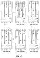
- FIGS. 1 ( a ) to 1 ( f )show schematic cross-sectional views of a conventional vertical trench MOSFET device. The figures show vertically expanding depletion regions as increasing reverse bias voltages are applied.
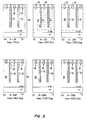
- FIGS. 2 ( a ) to 2 ( f )show schematic cross-sectional views of a vertical trench MOSFET device according to an embodiment of the invention.
- the figuresshow horizontally expanding depletion regions as increasing reverse bias voltages are applied.
- FIGS. 3 ( a ) to 3 ( f )show schematic cross sectional views of a vertical trench MOSFET device according to an embodiment of the invention.
- the figuresshow horizontally expanding depletion regions as increasing reverse bias voltages are applied.
- FIG. 4is a bar graph illustrating the various resistive components making up R DS(on) in various MOSFET devices with different breakdown voltage ratings.
- FIG. 5is a graph comparing reverse IV curves for conventional trench MOSFET devices with a reverse IV curve for a trench MOSFET device according to an embodiment of the invention.
- FIG. 6is a graph showing reverse IV curves for trench MOSFET devices with different P ⁇ stripe depths. The curves show the effect of varying P ⁇ stripe depths on BV DSS .
- FIG. 7is a graph showing reverse IV curves for trench MOSFET devices with different P ⁇ stripe widths. The curves show the effect of varying P ⁇ stripe widths on BV DSS .
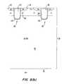
- FIGS. 8 ( a ) to 8 ( d )are cross-sectional views illustrating a method for forming a MOSFET device according to an embodiment of the invention.
- FIG. 8 ( e )shows a cross-sectional view of a MOSFET device with a stripe having a P ⁇ lining and a dielectric inner portion.
- the resistance of the epilayer in a MOSFETbecomes an increasingly significant component of R DS(on) for increasing MOSFET voltage breakdown ratings.
- computer simulationshave indicated that for a 30 volt N-channel trench MOSFET device, the epilayer resistance is about 30% or more of the total specific R DS(on) .
- the epilayer resistanceis about 75 to 90% of the total specific R DS(on) .
- the reduction of R DS(on)preferably takes place without degrading the breakdown voltage characteristics of the MOSFET device.
- the maximum breakdown voltage (BV DSS ) of a trench or planar DMOSFETdouble diffused metal oxide semiconductor field effect transistor
- BV DSSmaximum breakdown voltage
- the depletion regionis formed by applying a reverse bias voltage across the junction.
- the reverse-biased epilayer/well diodebreaks down and significant current starts to flow. Current flows between the source and drain by an avalanche multiplication process while the gate and the source are shorted together.
- FIGS. 1 ( a ) to 1 ( f )show schematic cross-sectional views of a conventional vertical trench MOSFET device.
- Each cross-sectionshows a plurality of gate structures 45 at a major surface of a semiconductor substrate 29 .
- the semiconductor substrate 29comprises an N ⁇ epilayer 32 and a drain region 31 .
- N+ source regions, P ⁇ wells, and P+ body regionsare shown.
- N+ source regions and P+ body regionsare not shown in FIGS. 1 ( b ) to 1 ( f ), 2 ( a ) to 2 ( f ), and 3 ( a ) to 3 ( f ).
- the N ⁇ epilayer 32has a resistivity of about 5.0 ohm-cm and an epilayer dopant concentration, N d (epi), of about 1 ⁇ 10 15 cm ⁇ 3 .
- the thickness of the N ⁇ epilayer 32is about 20 microns.
- the devicealso has an “effective” epilayer thickness (sometimes referred to as “effective epi”) of about 16.5 microns.
- the effective epilayer thicknessis the thickness of the epilayer after taking into account any up diffusion of atoms from the N+ drain region 31 and the formation of regions such as doped regions (e.g., P ⁇ wells) in the semiconductor substrate 29 .
- the effective epilayer thicknesscan be substantially equal to the distance between the bottom of a P+ body or a P ⁇ well and the endpoint of any up-diffused donors in the N ⁇ epilayer 32 from the N+ substrate 31 .
- the effective epilayer for the devicemay also include the drift region for the device.
- FIGS. 1 ( a ) to 1 ( f )also shows the maximum electric field established (“E max ”) as different reverse bias voltages are applied. As shown in the figures, as the reverse bias voltage is increased, E max also increases. If E max exceeds the critical electric field for a given dopant concentration, avalanche breakdown occurs. Consequently, E max is desirably less than the critical electric field.
- FIGS. 1 ( a ) to 1 ( f )respectively show how the depletion region 50 expands as increasing reverse bias voltages of 0V, 10V, 50V, 100V, 200V, and 250V are applied to the conventional trench MOSFET device. As shown in the figures, as greater reverse bias voltages are applied, the depletion region 50 spreads “vertically” in a direction from the P ⁇ well/epilayer interface to the N+ drain region 31 . This vertical growth of the depletion region forces the trade-off between lower R DS(on) and higher BV DSS in conventional trench MOSFET devices.
- the present inventionprovides an improved MOSFET device wherein the depletion region initially spreads “horizontally” as higher reverse bias voltages are applied.
- a number of additional (and preferably deep) trenchesare formed in the semiconductor substrate. These deep trenches are eventually used to form stripes that induce the formation of a horizontally spreading depletion region.
- the stripescomprise a material of the opposite type conductivity to the epilayer.
- the stripesmay comprise a P type material (e.g., a P, P+, or P ⁇ silicon) while the epilayer may comprise an N type material.
- Individual stripesmay be present between adjacent gate structures and can extend from the major surface of the semiconductor substrate and into the epilayer. The stripes can also extend any suitable distance into the epilayer.
- the stripesextend all the way to the epilayer/drain region interface.
- the presence of the stripesallows the use of a lower resistance epilayer without exceeding the critical electric field.
- R DS(on)can be reduced without detrimentally affecting other MOSFET device characteristics such as the breakdown voltage.
- FIGS. 2 ( a ) to 2 ( f )illustrate an embodiment of the invention. These figures illustrate how a depletion region spreads as greater reverse bias voltages are applied.
- the gate bias voltages applied in the examples shown in FIGS. 2 ( a ) to 2 ( f )are 0V, 1V, 2V, 10V, 200V, and 250V.
- each of the cross-sections of FIGS. 2 ( a ) to 2 ( f )include a plurality of trench gate structures 45 and a N ⁇ epilayer 32 .
- the N ⁇ epilayer 32is present in a semiconductor substrate 29 .
- a plurality of trenches forming stripes 35(e.g., P stripes) of the opposite conductivity type as the N ⁇ epilayer 32 are respectively disposed between adjacent gate structures 45 .
- the stripes 35comprise a P type material.
- the depletion region 50initially spreads “horizontally” away from the sides of the stripes 35 .
- the regions between adjacent stripes 35are quickly depleted of charge carriers as the depletion region 32 expands from the side-surfaces of adjacent stripes 35 .
- the depletion region 50spreads vertically in a direction from the ends of the stripes 35 towards the N+ drain region 31 .
- the epilayer 32 in the embodimentis depleted of charge carriers much more quickly than when depletion initially occurs in a “vertical” manner (e.g., as shown in FIGS. 1 ( a ) to 1 ( f )).
- the depletion region 50is similar in area with significantly less applied voltage (2V compared to 200 V).
- FIGS. 3 ( a ) to 3 ( f )show cross sections of another MOSFET device according to another embodiment of the invention.
- like elementsare denoted by like numerals in prior figures.
- the epilayer 50 in the MOSFET device shown in FIGS. 3 ( a ) to 3 ( f )has a resistivity of about 0.6 ohm-cm, a dopant concentration (N d ) of about 1 ⁇ 10 16 cm ⁇ 3 , a thickness of about 16 microns, and an effective epilayer thickness of about 12.5 microns.
- FIGS. 3 ( a ) to 3 ( f )respectively show how the depletion region 50 changes at reverse bias voltages of 0V, 10V, 50V, 100V, 200V, and 250V.
- the depletion region 50initially spreads “horizontally” as higher reverse bias voltages are applied.
- the maximum electric field (E max ) at each of these applied reverse bias voltagesdoes not exceed the critical field for avalanche breakdown for the stated dopant concentration. Consequently, a high breakdown voltage (e.g., 250 V) can be obtained while using a thinner and lower resistivity.
- the thinner and lower resistivity epilayeradvantageously results in a lower resistance epilayer and thus, a reduced R DS(on) value.
- the dimensions and doping level in the stripes 35are adjusted to balance the total charge in the stripes with the total charge in the epilayer depletion region 50 .
- FIG. 4shows a bar graph illustrating some components of R DS(on) for a number of N-channel MOSFET devices with different breakdown voltage ratings.
- Bar (a)represents the R DS(on) for a control N-channel 30 V MOSFET device at 500 A.
- Bars (b) to (f)refer to conventional trench N-channel MOSFET devices with respective breakdown voltages of 60, 80, 100, 150, and 200 V.
- the epilayer resistancehas a greater impact on R DS(on) .
- the epilayer resistanceconstitutes over 90% of the total specific R DS(on) .
- the epilayer resistancehas a significantly lower impact on R DS(on) .
- the epilayer resistancecan be lowered by incorporating trenched stripes in the epilayer. This reduces R DS(on) as compared to a similar conventional MOSFET device with a similar breakdown voltage rating.
- bar (g) in FIG. 4shows the improvement provided for a trench MOSFET device according to an exemplary embodiment of the invention.
- the epilayer resistancecan be significantly reduced when using trenched stripes having the opposite conductivity of the epilayer in a MOSFET device.
- the total specific R DS(on) for a 200 V trench N-channel MOSFET deviceis less than 1.4 milliohm-cm 2 .
- the total specific R DS(on)is about 7.5 milliohm-cm 2 . Accordingly, these exemplary embodiments of the invention can exhibit a greater than 5-fold reduction in R DS(on) than conventional trench MOSFET devices.
- FIGS. 5 to 11show graphs of reverse IV curves for MOSFET devices according to embodiments of the invention.
- FIG. 5is a graph showing reverse IV curves for conventional trench MOSFET devices and a MOSFET device according to an embodiment of the invention.
- FIG. 5shows IV curves 500 , 502 for two MOSFET devices without P ⁇ stripes.
- the first curve 500is for a MOSFET device with an epilayer resistance of 0.8 milliohm-cm and an epilayer thickness of 15 microns.
- the second curve 502is for a MOSFET device with an epilayer resistivity of 4.6 milliohm-cm and an epilayer thickness of 19.5 microns.
- the MOSFET device with the thicker epilayer and higher resistancehas a higher breakdown voltage.
- An IV curve 504 for an embodiment of the inventionis also shown in FIG. 5 .
- This exemplary embodimenthas an epilayer resistance of about 0.8 ohm-cm, an epilayer thickness of about 15 microns and a P ⁇ stripe about 12 microns deep.
- this device embodimenthas a relatively thin epilayer and a relatively low epilayer resistivity (and therefore a low R DS(on) ). It also has a breakdown voltage approaching 220 V. The breakdown voltage is comparable to the breakdown voltage exhibited by a conventional MOSFET device having a thicker and more resistive epilayer.
- FIG. 6shows reverse IV curves for MOSFET devices according to embodiments of the invention.
- the curvesshow the effect of varying the P ⁇ stripe depth on BV DSS .
- the epilayerhas a resistance of about 0.8 ohm-cm and a thickness of about 13 microns.
- the P ⁇ stripe widthis about 1.0 microns.
- the dopant concentration in the P ⁇ stripeis about 2.2 ⁇ 10 16 cm ⁇ 3 .
- the P ⁇ stripe depthwas varied at about 8, 10, and 12, microns.
- the IV curves for these variationsshow that the breakdown voltage increases as the depth of the P ⁇ stripes is increased.
- FIG. 7shows reverse IV curves for MOSFET devices according to embodiments of the invention.
- the curvesshow the effect of P ⁇ stripe width variations on BV DSS .
- the deviceshave an epilayer resistance of about 0.8 ohm-cm and a thickness of about 13 microns.
- the P ⁇ stripe depthis about 10 microns, and the dopant concentration in the P ⁇ stripe is about 2.2 ⁇ 10 16 cm ⁇ 3 .
- IV curves for P ⁇ stripes with widths of about 0.8, 1.0, and 1.2 micronsare shown. The IV curves show that the breakdown voltage is higher when the width of the P ⁇ stripes is equal to 1 micron.
- Embodiments of the present inventioncan be applied to both trench and planar MOSFET technologies.
- trench MOSFET devicesare preferred as they advantageously occupy less space than planar MOSFET devices.
- the breakdown voltage of the devicemay be from about 100 to about 400 volts in some embodiments.
- a method of manufacturing a MOSFET device according to the present inventionis described below in the context of a trenched gate process.
- the power trench MOSFET devicecomprises a semiconductor substrate 29 having a drain region 31 and an N ⁇ epitaxial portion 32 proximate the drain region 31 .
- the semiconductor substrate 29may comprise any suitable semiconductor material including Si, GaAs, etc.
- the drift region for the MOSFET devicemay be present in the epitaxial portion 32 of the semiconductor substrate 29 .
- a plurality of gate structures 45are proximate the major surface 28 of the semiconductor substrate 29 , and each gate structure 45 comprises a gate electrode 43 and a dielectric layer 44 on the gate electrode 43 .
- a plurality of N+ source regions 36are formed in the semiconductor substrate 29 .
- Each N+ source region 36is adjacent to one of the gate structures 45 and is formed in a plurality of P ⁇ well regions 34 , which are also formed in the semiconductor substrate 29 .
- Each P ⁇ well region 34is disposed adjacent to one of the gate structures 45 .
- a contact 41 for the source regions 36is present on the major surface 28 of the semiconductor substrate 29 .
- the contact 41may comprise a metal such as aluminum.
- other components which may be present in a MOSFET devicee.g., a passivation layer may not be shown in FIG. 8 ( d ).
- a trenched P ⁇ stripe 35is present in the semiconductor substrate 29 .
- a plurality of P ⁇ stripes 35may be respectively disposed between adjacent gate structures 45 when the gate structures 45 form an array of gate structures 45 .
- the P ⁇ stripe 35 shown in FIG. 8 ( d )is disposed between adjacent gate structures 45 .
- the P ⁇ stripe 35 shown in the figureis generally vertical and is oriented generally perpendicular to the orientation of the semiconductor substrate 29 .
- the P ⁇ stripe 35extends past the gate structures 45 and may penetrate most of the N ⁇ epitaxial portion 32 .
- the N ⁇ epitaxial portion 32 in this embodimentsurrounds the bottom and sides of the P ⁇ stripe 35 .
- the dopant concentration at the sides and below the P ⁇ stripe 35may be similar in this embodiment.
- the P ⁇ stripe 35has generally parallel sidewalls and a generally flat bottom. If the sidewalls are generally parallel, thin P ⁇ stripes 35 can be present between adjacent gate structures 45 .
- the pitch between gate structures 45can be minimized consequently resulting in MOSFET arrays of reduced size.
- the gate structure 45 (or gate electrode) pitchmay be less than about 10 microns (e.g., between about 4 to about 6 microns).
- the width of the P ⁇ stripes 35may be less than about 2 or 3 microns (e.g., between about 1 and about 2 microns).
- the stripe trenches in embodiments of the inventionare filled or lined with a material of the opposite doping to the epitaxial portion in the semiconductor substrate.
- An embodiment of this typeis shown in FIG. 8 ( e ) and is described in greater detail below.
- the stripemay comprise an inner dielectric portion and an outer semiconductor layer of the opposite conductivity type as the epitaxial portion.
- the inner dielectric portionmay comprise silicon oxide or air while the outer semiconductor layer may comprise P or N type epitaxial silicon.
- the presence of the doped stripesmay also be used as a heavy body to improve the ruggedness of the formed device.
- the presence of P ⁇ stripes penetrating the epilayeris believed to stabilize voltage variations in the device, thus increasing the device's reliability.
- a structure including a semiconductor substrate 29is provided.
- the semiconductor substrate 29may comprise an N+ drain region 31 and an N ⁇ epitaxial portion 32 .
- Gate trenches 30are formed proximate a major surface 28 of the semiconductor substrate 29 . These gate trenches 30 may be formed by using, for example, anisotropic etching methods well known in the art.
- gate structures 45are formed within the gate trenches 30 using methods well known in the art.
- Each gate structure 45comprises a dielectric layer 44 and a gate electrode 43 .
- the gate electrode 43may comprise polysilicon and the dielectric layer 44 may comprise silicon dioxide.
- Source regions, well regions, and other structuresmay also be formed in the semiconductor substrate 29 after or before forming the gate structures 45 .
- P ⁇ well regions 34are formed in the semiconductor substrate 29 and then N+ source regions 36 are formed in the semiconductor substrate 29 .
- Conventional ion implantation or conventional diffusion processesmay be used to form these regions. In this example, these doped regions are formed after the formation of the gate structures 45 .
- one or more stripe trenches 30are formed in the semiconductor substrate 29 .
- the stripe trench 30 shown in FIG. 8 ( c )may be formed, e.g., by an anisotropic etching process.
- the formed stripe trench 30extends from the major surface 28 of the semiconductor substrate 29 . It may extend any suitable distance past the gate structures 45 to the interface between the epitaxial portion 32 and the drain region 31 .
- the stripe trench 30terminates at a depth which is between half the thickness of the N ⁇ epitaxial portion 32 and the full thickness of the epitaxial portion 32 .
- the stripe trench 30may extend to the interface between the epitaxial portion 32 and the drain region 31 .
- a stripe 35is formed in the stripe trench 30 .
- the stripe 35comprises a material of the second conductivity type.
- the material of the second conductivity typeis an epitaxial material such as epitaxial P type silicon (e.g., P, P+, P ⁇ silicon).
- the stripe trenches 30may be filled using any suitable method including a selective epitaxial growth (SEG) process.
- the trenches 30may be filled with epitaxial silicon with doping occurring in-situ.
- the material of the second conductivity typemay completely fill the stripe trench 30 as shown in FIG. 8 ( d ) or may line the stripe trench 35 as shown in FIG. 8 ( e ).
- like numeralsdesignate like elements as in FIG. 8 ( d ).
- the stripe 35comprises a P ⁇ layer 35 ( a ) and an inner dielectric material 35 ( b ).
- the P ⁇ layer 35 ( a )may be deposited in the formed stripe trench first, and then the dielectric material 35 ( b ) may be deposited to fill the enclosure formed by the P ⁇ layer 35 ( a ).
- the inner dielectric materialmay be formed by oxidizing the P ⁇ layer 35 ( a ).
- the dielectric material 35 ( b )may comprise a material such as silicon dioxide or air.
- the stripe trench 30 and the stripes 35 of a second conductivity typeare preferably formed after at least one of the source regions 36 , the gate structures 45 , and the well regions 34 are formed.
- the stripes 35are not subjected to the high temperature processing used to form the gate structures 45 or the P ⁇ well regions 34 .
- the high temperature processinge.g., ion implantation, high temperature drives
- the P ⁇ well regionscan last as long as 1 to 3 hours at high temperatures (e.g., greater than 1100° C.).
- the formation of the P ⁇ stripes 35 in the semiconductor substrate 29does not detrimentally affect previously formed gate structures 45 , P ⁇ well regions 34 , or the N+ source regions 36 .
- Forming these device elements before forming the P ⁇ stripes 35reduces the likelihood that the P ⁇ stripes 35 in the epilayer will diffuse and lose their shape due to extended high temperature processing. If this occurs, the width of the P ⁇ stripes 35 may not be uniform down the P ⁇ stripe 35 and may decrease the effectiveness of the formed device. For example, dopant from a laterally enlarged P ⁇ stripe 35 could diffuse into the channel region of the MOSFET device thereby influencing the threshold voltage characteristics of the MOSFET device. Moreover, wider P ⁇ stripes can result in a larger gate structure 45 pitch, thus increasing the size of a corresponding array of gate structures 45 .
- Additional layersmay include a metal contact layer 41 and a passivation layer (not shown). These additional layers may be formed by any suitable method known in the art.
- embodiments of the inventionare not limited thereto.
- embodiments of the inventionhave been described with reference to N type semiconductors, P ⁇ stripes, etc. It is understood that the invention is not limited thereto and that the doping polarities of the structures shown and described could be reversed.
- P ⁇ stripesare mentioned in detail, it is understood that the stripes used in embodiments of the invention may be P or N type.
- the stripes or other device elementsmay also have any suitable acceptor or donor concentration (e.g., +, ++, ⁇ , ⁇ , etc.).
Landscapes
- Electrodes Of Semiconductors (AREA)
- Insulated Gate Type Field-Effect Transistor (AREA)
Abstract
Description
Claims (15)
Priority Applications (3)
| Application Number | Priority Date | Filing Date | Title |
|---|---|---|---|
| US10/741,464US6818513B2 (en) | 2001-01-30 | 2003-12-18 | Method of forming a field effect transistor having a lateral depletion structure |
| US10/934,969US20050029618A1 (en) | 2001-01-30 | 2004-09-03 | Structure and method of forming a dual-trench field effect transistor |
| US12/893,997US8829641B2 (en) | 2001-01-30 | 2010-09-29 | Method of forming a dual-trench field effect transistor |
Applications Claiming Priority (2)
| Application Number | Priority Date | Filing Date | Title |
|---|---|---|---|
| US09/774,780US6713813B2 (en) | 2001-01-30 | 2001-01-30 | Field effect transistor having a lateral depletion structure |
| US10/741,464US6818513B2 (en) | 2001-01-30 | 2003-12-18 | Method of forming a field effect transistor having a lateral depletion structure |
Related Parent Applications (1)
| Application Number | Title | Priority Date | Filing Date |
|---|---|---|---|
| US09/774,780DivisionUS6713813B2 (en) | 2001-01-30 | 2001-01-30 | Field effect transistor having a lateral depletion structure |
Related Child Applications (1)
| Application Number | Title | Priority Date | Filing Date |
|---|---|---|---|
| US10/934,969ContinuationUS20050029618A1 (en) | 2001-01-30 | 2004-09-03 | Structure and method of forming a dual-trench field effect transistor |
Publications (2)
| Publication Number | Publication Date |
|---|---|
| US20040132252A1 US20040132252A1 (en) | 2004-07-08 |
| US6818513B2true US6818513B2 (en) | 2004-11-16 |
Family
ID=25102275
Family Applications (3)
| Application Number | Title | Priority Date | Filing Date |
|---|---|---|---|
| US10/741,464Expired - LifetimeUS6818513B2 (en) | 2001-01-30 | 2003-12-18 | Method of forming a field effect transistor having a lateral depletion structure |
| US10/934,969AbandonedUS20050029618A1 (en) | 2001-01-30 | 2004-09-03 | Structure and method of forming a dual-trench field effect transistor |
| US12/893,997Expired - LifetimeUS8829641B2 (en) | 2001-01-30 | 2010-09-29 | Method of forming a dual-trench field effect transistor |
Family Applications After (2)
| Application Number | Title | Priority Date | Filing Date |
|---|---|---|---|
| US10/934,969AbandonedUS20050029618A1 (en) | 2001-01-30 | 2004-09-03 | Structure and method of forming a dual-trench field effect transistor |
| US12/893,997Expired - LifetimeUS8829641B2 (en) | 2001-01-30 | 2010-09-29 | Method of forming a dual-trench field effect transistor |
Country Status (1)
| Country | Link |
|---|---|
| US (3) | US6818513B2 (en) |
Cited By (20)
| Publication number | Priority date | Publication date | Assignee | Title |
|---|---|---|---|---|
| US20050023605A1 (en)* | 2003-07-31 | 2005-02-03 | Michael Amato | High voltage semiconductor device having an increased breakdown voltage relative to its on-resistance |
| US20050275016A1 (en)* | 2004-06-04 | 2005-12-15 | International Rectifier Corp. | Deep trench super switch device |
| US20080111207A1 (en)* | 2006-11-15 | 2008-05-15 | Lee Jae-Gil | High-Voltage Semiconductor Device and Method of Fabricating the Same |
| US20090189216A1 (en)* | 2008-01-25 | 2009-07-30 | Infineon Technologies Austria Ag | Semiconductor component including a drift zone and a drift control zone |
| US7732876B2 (en) | 2004-08-03 | 2010-06-08 | Fairchild Semiconductor Corporation | Power transistor with trench sinker for contacting the backside |
| US20100163846A1 (en)* | 2008-12-31 | 2010-07-01 | Hamza Yilmaz | Nano-tube mosfet technology and devices |
| US20100317158A1 (en)* | 2009-06-12 | 2010-12-16 | Alpha & Omega Semiconductor, Inc. | Method for Forming Nanotube Semiconductor Devices |
| US20100314659A1 (en)* | 2009-06-12 | 2010-12-16 | Alpha & Omega Semiconductor, Inc. | Nanotube Semiconductor Devices |
| US20110127601A1 (en)* | 2009-12-02 | 2011-06-02 | Suku Kim | Semiconductor Devices and Methods for Making the Same |
| US20110198689A1 (en)* | 2010-02-17 | 2011-08-18 | Suku Kim | Semiconductor devices containing trench mosfets with superjunctions |
| US20120276701A1 (en)* | 2011-04-27 | 2012-11-01 | Yedinak Joseph A | Superjunction Structures for Power Devices and Methods of Manufacture |
| US8772868B2 (en) | 2011-04-27 | 2014-07-08 | Fairchild Semiconductor Corporation | Superjunction structures for power devices and methods of manufacture |
| US8786010B2 (en) | 2011-04-27 | 2014-07-22 | Fairchild Semiconductor Corporation | Superjunction structures for power devices and methods of manufacture |
| US8786045B2 (en) | 2003-05-20 | 2014-07-22 | Fairchild Semiconductor Corporation | Power semiconductor devices having termination structures |
| US8829641B2 (en) | 2001-01-30 | 2014-09-09 | Fairchild Semiconductor Corporation | Method of forming a dual-trench field effect transistor |
| US8836028B2 (en) | 2011-04-27 | 2014-09-16 | Fairchild Semiconductor Corporation | Superjunction structures for power devices and methods of manufacture |
| US8928077B2 (en) | 2007-09-21 | 2015-01-06 | Fairchild Semiconductor Corporation | Superjunction structures for power devices |
| US20150118810A1 (en)* | 2013-10-24 | 2015-04-30 | Madhur Bobde | Buried field ring field effect transistor (buf-fet) integrated with cells implanted with hole supply path |
| US9431481B2 (en) | 2008-09-19 | 2016-08-30 | Fairchild Semiconductor Corporation | Superjunction structures for power devices and methods of manufacture |
| US9508805B2 (en) | 2008-12-31 | 2016-11-29 | Alpha And Omega Semiconductor Incorporated | Termination design for nanotube MOSFET |
Families Citing this family (9)
| Publication number | Priority date | Publication date | Assignee | Title |
|---|---|---|---|---|
| WO2008106235A1 (en)* | 2007-03-01 | 2008-09-04 | International Rectifier Corporation | Trench mosgated device with deep trench between gate trenches |
| CN102751190B (en)* | 2011-04-22 | 2014-12-03 | 科轩微电子股份有限公司 | Trench type power metal oxide semiconductor structure and manufacturing method with fast switching capability |
| CN103151268B (en)* | 2013-03-21 | 2016-02-03 | 矽力杰半导体技术(杭州)有限公司 | A kind of vertical bilateral diffusion field-effect pipe and manufacturing process thereof |
| US9484404B2 (en) | 2014-01-29 | 2016-11-01 | Stmicroelectronics S.R.L. | Electronic device of vertical MOS type with termination trenches having variable depth |
| CN105226090B (en)* | 2015-11-10 | 2018-07-13 | 株洲中车时代电气股份有限公司 | A kind of igbt and preparation method thereof |
| CN110896026A (en) | 2019-11-22 | 2020-03-20 | 矽力杰半导体技术(杭州)有限公司 | Trench type MOSFET structure and manufacturing method thereof |
| CN111129152B (en)* | 2019-12-17 | 2023-09-26 | 杭州芯迈半导体技术有限公司 | Trench MOSFET structure and manufacturing method |
| CN111554746B (en) | 2020-04-23 | 2022-09-16 | 杭州芯迈半导体技术有限公司 | Silicon carbide MOSFET device and manufacturing method thereof |
| CN114188395A (en)* | 2021-10-09 | 2022-03-15 | 无锡先瞳半导体科技有限公司 | Charge compensation type shielded gate trench power device and preparation method thereof |
Citations (100)
| Publication number | Priority date | Publication date | Assignee | Title |
|---|---|---|---|---|
| US4579621A (en) | 1983-07-08 | 1986-04-01 | Mitsubishi Denki Kabushiki Kaisha | Selective epitaxial growth method |
| US4638344A (en) | 1979-10-09 | 1987-01-20 | Cardwell Jr Walter T | Junction field-effect transistor controlled by merged depletion regions |
| US4698653A (en) | 1979-10-09 | 1987-10-06 | Cardwell Jr Walter T | Semiconductor devices controlled by depletion regions |
| US4754310A (en) | 1980-12-10 | 1988-06-28 | U.S. Philips Corp. | High voltage semiconductor device |
| CN1036666A (en) | 1988-02-22 | 1989-10-25 | 亚瑞亚·勃朗·勃威力有限公司 | Field-effect controlled bipolar power semiconductor device and manufacturing method thereof |
| US5072266A (en) | 1988-12-27 | 1991-12-10 | Siliconix Incorporated | Trench DMOS power transistor with field-shaping body profile and three-dimensional geometry |
| US5216275A (en) | 1991-03-19 | 1993-06-01 | University Of Electronic Science And Technology Of China | Semiconductor power devices with alternating conductivity type high-voltage breakdown regions |
| US5219793A (en) | 1991-06-03 | 1993-06-15 | Motorola Inc. | Method for forming pitch independent contacts and a semiconductor device having the same |
| US5275965A (en) | 1992-11-25 | 1994-01-04 | Micron Semiconductor, Inc. | Trench isolation using gated sidewalls |
| US5294824A (en) | 1992-07-31 | 1994-03-15 | Motorola, Inc. | High voltage transistor having reduced on-resistance |
| US5300447A (en) | 1992-09-29 | 1994-04-05 | Texas Instruments Incorporated | Method of manufacturing a minimum scaled transistor |
| US5326711A (en) | 1993-01-04 | 1994-07-05 | Texas Instruments Incorporated | High performance high voltage vertical transistor and method of fabrication |
| US5405794A (en) | 1994-06-14 | 1995-04-11 | Philips Electronics North America Corporation | Method of producing VDMOS device of increased power density |
| US5424231A (en) | 1994-08-09 | 1995-06-13 | United Microelectronics Corp. | Method for manufacturing a VDMOS transistor |
| US5438215A (en) | 1993-03-25 | 1995-08-01 | Siemens Aktiengesellschaft | Power MOSFET |
| US5473180A (en) | 1993-07-12 | 1995-12-05 | U.S. Philips Corporation | Semiconductor device with an MOST provided with an extended drain region for high voltages |
| US5581100A (en) | 1994-08-30 | 1996-12-03 | International Rectifier Corporation | Trench depletion MOSFET |
| US5583065A (en) | 1994-11-23 | 1996-12-10 | Sony Corporation | Method of making a MOS semiconductor device |
| US5592005A (en) | 1995-03-31 | 1997-01-07 | Siliconix Incorporated | Punch-through field effect transistor |
| US5629543A (en)* | 1995-08-21 | 1997-05-13 | Siliconix Incorporated | Trenched DMOS transistor with buried layer for reduced on-resistance and ruggedness |
| US5656843A (en) | 1992-08-05 | 1997-08-12 | U.S. Philips Corporation | Semiconductor device having a vertical insulated gate field effect device and a breakdown region remote from the gate |
| US5780343A (en) | 1995-12-20 | 1998-07-14 | National Semiconductor Corporation | Method of producing high quality silicon surface for selective epitaxial growth of silicon |
| US5801417A (en) | 1988-05-17 | 1998-09-01 | Advanced Power Technology, Inc. | Self-aligned power MOSFET device with recessed gate and source |
| US5895951A (en)* | 1996-04-05 | 1999-04-20 | Megamos Corporation | MOSFET structure and fabrication process implemented by forming deep and narrow doping regions through doping trenches |
| US5972741A (en) | 1996-10-31 | 1999-10-26 | Sanyo Electric Co., Ltd. | Method of manufacturing semiconductor device |
| US5973360A (en) | 1996-03-20 | 1999-10-26 | Siemens Aktiengesellschaft | Field effect-controllable semiconductor component |
| US6005271A (en) | 1997-11-05 | 1999-12-21 | Magepower Semiconductor Corp. | Semiconductor cell array with high packing density |
| EP0976024A2 (en) | 1998-02-16 | 2000-02-02 | ECT AB Eye Control Technique | Eye controlled opto-electric input/output interface |
| JP2000040872A (en) | 1998-07-24 | 2000-02-08 | Senju Metal Ind Co Ltd | Method of soldering printed board, and jet solder vessel |
| JP2000040822A (en) | 1998-07-24 | 2000-02-08 | Fuji Electric Co Ltd | Super junction semiconductor device and method of manufacturing the same |
| US6037632A (en) | 1995-11-06 | 2000-03-14 | Kabushiki Kaisha Toshiba | Semiconductor device |
| US6040600A (en) | 1997-02-10 | 2000-03-21 | Mitsubishi Denki Kabushiki Kaisha | Trenched high breakdown voltage semiconductor device |
| US6049108A (en) | 1995-06-02 | 2000-04-11 | Siliconix Incorporated | Trench-gated MOSFET with bidirectional voltage clamping |
| US6057558A (en) | 1997-03-05 | 2000-05-02 | Denson Corporation | Silicon carbide semiconductor device and manufacturing method thereof |
| US6066878A (en) | 1997-11-10 | 2000-05-23 | Intersil Corporation | High voltage semiconductor structure |
| JP2000156978A (en) | 1998-11-17 | 2000-06-06 | Fuji Electric Co Ltd | Soft switching circuit |
| WO2000033386A2 (en) | 1998-11-28 | 2000-06-08 | Koninklijke Philips Electronics N.V. | Trench-gate semiconductor devices and their manufacture |
| US6084264A (en) | 1998-11-25 | 2000-07-04 | Siliconix Incorporated | Trench MOSFET having improved breakdown and on-resistance characteristics |
| US6084268A (en) | 1996-03-05 | 2000-07-04 | Semiconductor Components Industries, Llc | Power MOSFET device having low on-resistance and method |
| US6097063A (en) | 1996-01-22 | 2000-08-01 | Fuji Electric Co., Ltd. | Semiconductor device having a plurality of parallel drift regions |
| JP2000277728A (en) | 1999-03-25 | 2000-10-06 | Nec Kansai Ltd | Insulated gate semiconductor device and method of manufacturing the same |
| JP2000277726A (en) | 1999-03-23 | 2000-10-06 | Toshiba Corp | High voltage semiconductor device |
| WO2000068998A1 (en) | 1999-05-06 | 2000-11-16 | C.P. Clare Corporation | High voltage mosfet structures |
| WO2000068997A1 (en) | 1999-05-06 | 2000-11-16 | C.P. Clare Corporation | Mosfet with field reducing trenches in body region |
| US6156611A (en) | 1998-07-20 | 2000-12-05 | Motorola, Inc. | Method of fabricating vertical FET with sidewall gate electrode |
| US6163052A (en) | 1997-04-04 | 2000-12-19 | Advanced Micro Devices, Inc. | Trench-gated vertical combination JFET and MOSFET devices |
| US6168983B1 (en) | 1996-11-05 | 2001-01-02 | Power Integrations, Inc. | Method of making a high-voltage transistor with multiple lateral conduction layers |
| US6171935B1 (en) | 1998-05-06 | 2001-01-09 | Siemens Aktiengesellschaft | Process for producing an epitaxial layer with laterally varying doping |
| JP2001015752A (en) | 1998-11-11 | 2001-01-19 | Fuji Electric Co Ltd | Super junction semiconductor device and method of manufacturing the same |
| JP2001015448A (en) | 1999-06-28 | 2001-01-19 | Toshiba Corp | Method for manufacturing semiconductor device |
| WO2001006557A1 (en) | 1999-07-14 | 2001-01-25 | Koninklijke Philips Electronics N.V. | Method of making a charge compensation semiconductor device using neutron transmutation |
| WO2001006550A1 (en) | 1999-07-15 | 2001-01-25 | Koninklijke Philips Electronics N.V. | Method of making a charge compensation semiconductor device using direct bonding and corresponding device |
| US6184545B1 (en) | 1997-09-12 | 2001-02-06 | Infineon Technologies Ag | Semiconductor component with metal-semiconductor junction with low reverse current |
| US6184555B1 (en) | 1996-02-05 | 2001-02-06 | Siemens Aktiengesellschaft | Field effect-controlled semiconductor component |
| US6188105B1 (en) | 1999-04-01 | 2001-02-13 | Intersil Corporation | High density MOS-gated power device and process for forming same |
| US6191447B1 (en) | 1999-05-28 | 2001-02-20 | Micro-Ohm Corporation | Power semiconductor devices that utilize tapered trench-based insulating regions to improve electric field profiles in highly doped drift region mesas and methods of forming same |
| US6201279B1 (en) | 1998-10-22 | 2001-03-13 | Infineon Technologies Ag | Semiconductor component having a small forward voltage and high blocking ability |
| US6204097B1 (en) | 1999-03-01 | 2001-03-20 | Semiconductor Components Industries, Llc | Semiconductor device and method of manufacture |
| US6207994B1 (en) | 1996-11-05 | 2001-03-27 | Power Integrations, Inc. | High-voltage transistor with multi-layer conduction region |
| JP2001102577A (en) | 1999-09-30 | 2001-04-13 | Toshiba Corp | Semiconductor device |
| JP2001111041A (en) | 1998-11-12 | 2001-04-20 | Fuji Electric Co Ltd | Super junction semiconductor device and method of manufacturing the same |
| US6225649B1 (en) | 1998-01-22 | 2001-05-01 | Mitsubishi Denki Kabushiki Kaisha | Insulated-gate bipolar semiconductor device |
| JP2001135819A (en) | 1999-08-23 | 2001-05-18 | Fuji Electric Co Ltd | Super junction semiconductor device |
| JP2001144292A (en) | 1999-11-17 | 2001-05-25 | Denso Corp | Silicon carbide semiconductor device |
| US6239463B1 (en) | 1997-08-28 | 2001-05-29 | Siliconix Incorporated | Low resistance power MOSFET or other device containing silicon-germanium layer |
| US6239464B1 (en) | 1998-01-08 | 2001-05-29 | Kabushiki Kaisha Toshiba | Semiconductor gate trench with covered open ends |
| WO2001045155A1 (en) | 1999-12-15 | 2001-06-21 | Koninklijke Philips Electronics N.V. | Manufacture of semiconductor material and devices using that material |
| US6271562B1 (en) | 1998-02-27 | 2001-08-07 | Infineon Technologies Ag | Semiconductor component which can be controlled by a field effect |
| US6274905B1 (en) | 1999-06-30 | 2001-08-14 | Fairchild Semiconductor Corporation | Trench structure substantially filled with high-conductivity material |
| WO2001059847A2 (en) | 2000-02-12 | 2001-08-16 | Koninklijke Philips Electronics N.V. | Insulated gate semiconductor device having field shaping regions |
| US6281547B1 (en) | 1997-05-08 | 2001-08-28 | Megamos Corporation | Power transistor cells provided with reliable trenched source contacts connected to narrower source manufactured without a source mask |
| JP2001244461A (en) | 2000-02-28 | 2001-09-07 | Toyota Central Res & Dev Lab Inc | Vertical semiconductor device |
| US6291856B1 (en) | 1998-11-12 | 2001-09-18 | Fuji Electric Co., Ltd. | Semiconductor device with alternating conductivity type layer and method of manufacturing the same |
| US6297534B1 (en) | 1998-10-07 | 2001-10-02 | Kabushiki Kaisha Toshiba | Power semiconductor device |
| US20010028083A1 (en) | 2000-02-09 | 2001-10-11 | Yasuhiko Onishi | Super-junction semiconductor device and method of manufacturing the same |
| US6307246B1 (en) | 1998-07-23 | 2001-10-23 | Mitsubishi Denki Kabushiki Kaisha | Semiconductor resurf devices formed by oblique trench implantation |
| US20010032998A1 (en) | 2000-03-17 | 2001-10-25 | Susumu Iwamoto | Super-junction semiconductor device and method of manufacturing the same |
| US6309920B1 (en) | 1997-07-22 | 2001-10-30 | Siemens Aktiengesellschaft | Bipolar transistor which can be controlled by field effect and method for producing the same |
| US6313482B1 (en) | 1999-05-17 | 2001-11-06 | North Carolina State University | Silicon carbide power devices having trench-based silicon carbide charge coupling regions therein |
| JP2001313391A (en) | 2000-05-01 | 2001-11-09 | Fuji Electric Co Ltd | Semiconductor device |
| US6316806B1 (en) | 1999-03-31 | 2001-11-13 | Fairfield Semiconductor Corporation | Trench transistor with a self-aligned source |
| US20010041400A1 (en) | 2000-05-15 | 2001-11-15 | International Rectifier Corp. | Angle implant process for cellular deep trench sidewall doping |
| US6326656B1 (en) | 1998-06-24 | 2001-12-04 | Siemens Aktiengesellschaft | Lateral high-voltage transistor |
| WO2001095398A1 (en) | 2000-06-02 | 2001-12-13 | General Semiconductor, Inc. | Power mosfet and method of making the same |
| US20010050394A1 (en) | 2000-04-27 | 2001-12-13 | Yasuhiko Onishi | Lateral super-junction semiconductor device |
| WO2001095385A1 (en) | 2000-06-02 | 2001-12-13 | General Semiconductor, Inc. | Method of making a power mosfet |
| US6337499B1 (en) | 1997-11-03 | 2002-01-08 | Infineon Technologies Ag | Semiconductor component |
| US6346469B1 (en) | 2000-01-03 | 2002-02-12 | Motorola, Inc. | Semiconductor device and a process for forming the semiconductor device |
| US6353252B1 (en) | 1999-07-29 | 2002-03-05 | Kabushiki Kaisha Toshiba | High breakdown voltage semiconductor device having trenched film connected to electrodes |
| US6362112B1 (en) | 2000-11-08 | 2002-03-26 | Fabtech, Inc. | Single step etched moat |
| US6362505B1 (en) | 1998-11-27 | 2002-03-26 | Siemens Aktiengesellschaft | MOS field-effect transistor with auxiliary electrode |
| US6365930B1 (en) | 1999-06-03 | 2002-04-02 | Stmicroelectronics S.R.L. | Edge termination of semiconductor devices for high voltages with resistive voltage divider |
| US6368921B1 (en) | 1999-09-28 | 2002-04-09 | U.S. Philips Corporation | Manufacture of trench-gate semiconductor devices |
| US6376314B1 (en) | 1997-11-07 | 2002-04-23 | Zetex Plc. | Method of semiconductor device fabrication |
| US6384456B1 (en) | 1997-09-30 | 2002-05-07 | Infineon Technologies Ag | Field-effect transistor having a high packing density and method for fabricating it |
| US6388287B2 (en) | 1998-09-11 | 2002-05-14 | Infineon Technologies Ag | Switch mode power supply with reduced switching losses |
| US6400003B1 (en) | 1998-02-12 | 2002-06-04 | Koninklijke Philips Electronics N.V. | High voltage MOSFET with geometrical depletion layer enhancement |
| US20020066924A1 (en) | 1999-06-03 | 2002-06-06 | Blanchard Richard A. | High voltage power MOSFET having low on-resistance |
| US6653691B2 (en)* | 2000-11-16 | 2003-11-25 | Silicon Semiconductor Corporation | Radio frequency (RF) power devices having faraday shield layers therein |
| US6750105B2 (en)* | 2001-09-07 | 2004-06-15 | Power Integrations, Inc. | Method of fabricating a high-voltage transistor with a multi-layered extended drain structure |
Family Cites Families (171)
| Publication number | Priority date | Publication date | Assignee | Title |
|---|---|---|---|---|
| US3404295A (en) | 1964-11-30 | 1968-10-01 | Motorola Inc | High frequency and voltage transistor with added region for punch-through protection |
| US3412297A (en) | 1965-12-16 | 1968-11-19 | United Aircraft Corp | Mos field-effect transistor with a onemicron vertical channel |
| US3497777A (en)* | 1967-06-13 | 1970-02-24 | Stanislas Teszner | Multichannel field-effect semi-conductor device |
| US3564356A (en)* | 1968-10-24 | 1971-02-16 | Tektronix Inc | High voltage integrated circuit transistor |
| US3660697A (en)* | 1970-02-16 | 1972-05-02 | Bell Telephone Labor Inc | Monolithic semiconductor apparatus adapted for sequential charge transfer |
| US4003072A (en)* | 1972-04-20 | 1977-01-11 | Sony Corporation | Semiconductor device with high voltage breakdown resistance |
| US4337474A (en) | 1978-08-31 | 1982-06-29 | Mitsubishi Denki Kabushiki Kaisha | Semiconductor device |
| US4345265A (en) | 1980-04-14 | 1982-08-17 | Supertex, Inc. | MOS Power transistor with improved high-voltage capability |
| US4868624A (en) | 1980-05-09 | 1989-09-19 | Regents Of The University Of Minnesota | Channel collector transistor |
| US4300150A (en) | 1980-06-16 | 1981-11-10 | North American Philips Corporation | Lateral double-diffused MOS transistor device |
| US4326332A (en)* | 1980-07-28 | 1982-04-27 | International Business Machines Corp. | Method of making a high density V-MOS memory array |
| EP0051693B1 (en)* | 1980-11-12 | 1985-06-19 | Ibm Deutschland Gmbh | Electrically switchable read-only memory |
| US4974059A (en) | 1982-12-21 | 1990-11-27 | International Rectifier Corporation | Semiconductor high-power mosfet device |
| US4639761A (en)* | 1983-12-16 | 1987-01-27 | North American Philips Corporation | Combined bipolar-field effect transistor resurf devices |
| FR2566179B1 (en)* | 1984-06-14 | 1986-08-22 | Commissariat Energie Atomique | METHOD FOR SELF-POSITIONING OF A LOCALIZED FIELD OXIDE WITH RESPECT TO AN ISOLATION TRENCH |
| US4774556A (en) | 1985-07-25 | 1988-09-27 | Nippondenso Co., Ltd. | Non-volatile semiconductor memory device |
| US5262336A (en) | 1986-03-21 | 1993-11-16 | Advanced Power Technology, Inc. | IGBT process to produce platinum lifetime control |
| US5034785A (en) | 1986-03-24 | 1991-07-23 | Siliconix Incorporated | Planar vertical channel DMOS structure |
| US4716126A (en) | 1986-06-05 | 1987-12-29 | Siliconix Incorporated | Fabrication of double diffused metal oxide semiconductor transistor |
| US5607511A (en)* | 1992-02-21 | 1997-03-04 | International Business Machines Corporation | Method and apparatus for low temperature, low pressure chemical vapor deposition of epitaxial silicon layers |
| US4746630A (en)* | 1986-09-17 | 1988-05-24 | Hewlett-Packard Company | Method for producing recessed field oxide with improved sidewall characteristics |
| US4941026A (en) | 1986-12-05 | 1990-07-10 | General Electric Company | Semiconductor devices exhibiting minimum on-resistance |
| JP2577330B2 (en) | 1986-12-11 | 1997-01-29 | 新技術事業団 | Method of manufacturing double-sided gate static induction thyristor |
| US5105243A (en)* | 1987-02-26 | 1992-04-14 | Kabushiki Kaisha Toshiba | Conductivity-modulation metal oxide field effect transistor with single gate structure |
| US4821095A (en)* | 1987-03-12 | 1989-04-11 | General Electric Company | Insulated gate semiconductor device with extra short grid and method of fabrication |
| US4823176A (en)* | 1987-04-03 | 1989-04-18 | General Electric Company | Vertical double diffused metal oxide semiconductor (VDMOS) device including high voltage junction exhibiting increased safe operating area |
| US4801986A (en)* | 1987-04-03 | 1989-01-31 | General Electric Company | Vertical double diffused metal oxide semiconductor VDMOS device with increased safe operating area and method |
| US5164325A (en) | 1987-10-08 | 1992-11-17 | Siliconix Incorporated | Method of making a vertical current flow field effect transistor |
| US4893160A (en)* | 1987-11-13 | 1990-01-09 | Siliconix Incorporated | Method for increasing the performance of trenched devices and the resulting structure |
| US4914058A (en)* | 1987-12-29 | 1990-04-03 | Siliconix Incorporated | Grooved DMOS process with varying gate dielectric thickness |
| US4967245A (en) | 1988-03-14 | 1990-10-30 | Siliconix Incorporated | Trench power MOSFET device |
| KR0173111B1 (en) | 1988-06-02 | 1999-02-01 | 야마무라 가쯔미 | Trench Gate MOS FET |
| JPH0216763A (en)* | 1988-07-05 | 1990-01-19 | Toshiba Corp | Manufacturing method of semiconductor device |
| US4853345A (en) | 1988-08-22 | 1989-08-01 | Delco Electronics Corporation | Process for manufacture of a vertical DMOS transistor |
| US5268311A (en) | 1988-09-01 | 1993-12-07 | International Business Machines Corporation | Method for forming a thin dielectric layer on a substrate |
| US5111253A (en)* | 1989-05-09 | 1992-05-05 | General Electric Company | Multicellular FET having a Schottky diode merged therewith |
| US4992390A (en)* | 1989-07-06 | 1991-02-12 | General Electric Company | Trench gate structure with thick bottom oxide |
| EP0450082B1 (en)* | 1989-08-31 | 2004-04-28 | Denso Corporation | Insulated gate bipolar transistor |
| US5248894A (en) | 1989-10-03 | 1993-09-28 | Harris Corporation | Self-aligned channel stop for trench-isolated island |
| US5071782A (en) | 1990-06-28 | 1991-12-10 | Texas Instruments Incorporated | Vertical memory cell array and method of fabrication |
| US5079608A (en)* | 1990-11-06 | 1992-01-07 | Harris Corporation | Power MOSFET transistor circuit with active clamp |
| US5164802A (en) | 1991-03-20 | 1992-11-17 | Harris Corporation | Power vdmosfet with schottky on lightly doped drain of lateral driver fet |
| KR940006702B1 (en) | 1991-06-14 | 1994-07-25 | 금성일렉트론 주식회사 | Manufacturing method of mospat |
| US5298761A (en)* | 1991-06-17 | 1994-03-29 | Nikon Corporation | Method and apparatus for exposure process |
| JP2570022B2 (en) | 1991-09-20 | 1997-01-08 | 株式会社日立製作所 | Constant voltage diode, power conversion device using the same, and method of manufacturing constant voltage diode |
| JPH0613627A (en) | 1991-10-08 | 1994-01-21 | Semiconductor Energy Lab Co Ltd | Semiconductor device and manufacturing method thereof |
| JPH05304297A (en) | 1992-01-29 | 1993-11-16 | Nec Corp | Power semiconductor device and manufacturing method thereof |
| US5315142A (en) | 1992-03-23 | 1994-05-24 | International Business Machines Corporation | High performance trench EEPROM cell |
| JP2904635B2 (en) | 1992-03-30 | 1999-06-14 | 株式会社東芝 | Semiconductor device and manufacturing method thereof |
| US5554862A (en) | 1992-03-31 | 1996-09-10 | Kabushiki Kaisha Toshiba | Power semiconductor device |
| JPH06196723A (en)* | 1992-04-28 | 1994-07-15 | Mitsubishi Electric Corp | Semiconductor device and manufacture thereof |
| US5640034A (en) | 1992-05-18 | 1997-06-17 | Texas Instruments Incorporated | Top-drain trench based resurf DMOS transistor structure |
| US5233215A (en) | 1992-06-08 | 1993-08-03 | North Carolina State University At Raleigh | Silicon carbide power MOSFET with floating field ring and floating field plate |
| US5430324A (en)* | 1992-07-23 | 1995-07-04 | Siliconix, Incorporated | High voltage transistor having edge termination utilizing trench technology |
| US5558313A (en) | 1992-07-24 | 1996-09-24 | Siliconix Inorporated | Trench field effect transistor with reduced punch-through susceptibility and low RDSon |
| JPH06163907A (en) | 1992-11-20 | 1994-06-10 | Hitachi Ltd | Voltage-driven semiconductor device |
| DE4300806C1 (en) | 1993-01-14 | 1993-12-23 | Siemens Ag | Vertical MOS transistor prodn. - with reduced trench spacing, without parasitic bipolar effects |
| US5418376A (en)* | 1993-03-02 | 1995-05-23 | Toyo Denki Seizo Kabushiki Kaisha | Static induction semiconductor device with a distributed main electrode structure and static induction semiconductor device with a static induction main electrode shorted structure |
| US5341011A (en) | 1993-03-15 | 1994-08-23 | Siliconix Incorporated | Short channel trenched DMOS transistor |
| US5365102A (en) | 1993-07-06 | 1994-11-15 | North Carolina State University | Schottky barrier rectifier with MOS trench |
| JPH07122749A (en) | 1993-09-01 | 1995-05-12 | Toshiba Corp | Semiconductor device and manufacturing method thereof |
| JP3400846B2 (en) | 1994-01-20 | 2003-04-28 | 三菱電機株式会社 | Semiconductor device having trench structure and method of manufacturing the same |
| US5429977A (en) | 1994-03-11 | 1995-07-04 | Industrial Technology Research Institute | Method for forming a vertical transistor with a stacked capacitor DRAM cell |
| US5434435A (en) | 1994-05-04 | 1995-07-18 | North Carolina State University | Trench gate lateral MOSFET |
| DE4417150C2 (en)* | 1994-05-17 | 1996-03-14 | Siemens Ag | Method for producing an arrangement with self-reinforcing dynamic MOS transistor memory cells |
| US5583368A (en)* | 1994-08-11 | 1996-12-10 | International Business Machines Corporation | Stacked devices |
| EP0698919B1 (en) | 1994-08-15 | 2002-01-16 | Siliconix Incorporated | Trenched DMOS transistor fabrication using seven masks |
| US5674766A (en)* | 1994-12-30 | 1997-10-07 | Siliconix Incorporated | Method of making a trench MOSFET with multi-resistivity drain to provide low on-resistance by varying dopant concentration in epitaxial layer |
| US5597765A (en)* | 1995-01-10 | 1997-01-28 | Siliconix Incorporated | Method for making termination structure for power MOSFET |
| JPH08204179A (en) | 1995-01-26 | 1996-08-09 | Fuji Electric Co Ltd | Silicon Carbide Trench MOSFET |
| US5670803A (en) | 1995-02-08 | 1997-09-23 | International Business Machines Corporation | Three-dimensional SRAM trench structure and fabrication method therefor |
| JP3325736B2 (en)* | 1995-02-09 | 2002-09-17 | 三菱電機株式会社 | Insulated gate semiconductor device |
| EP0726603B1 (en) | 1995-02-10 | 1999-04-21 | SILICONIX Incorporated | Trenched field effect transistor with PN depletion barrier |
| JP3291957B2 (en)* | 1995-02-17 | 2002-06-17 | 富士電機株式会社 | Vertical trench MISFET and method of manufacturing the same |
| US5595927A (en)* | 1995-03-17 | 1997-01-21 | Taiwan Semiconductor Manufacturing Company Ltd. | Method for making self-aligned source/drain mask ROM memory cell using trench etched channel |
| JPH08306914A (en)* | 1995-04-27 | 1996-11-22 | Nippondenso Co Ltd | Semiconductor device and manufacturing method thereof |
| US5567634A (en) | 1995-05-01 | 1996-10-22 | National Semiconductor Corporation | Method of fabricating self-aligned contact trench DMOS transistors |
| US5648670A (en) | 1995-06-07 | 1997-07-15 | Sgs-Thomson Microelectronics, Inc. | Trench MOS-gated device with a minimum number of masks |
| US5689128A (en) | 1995-08-21 | 1997-11-18 | Siliconix Incorporated | High density trenched DMOS transistor |
| FR2738394B1 (en) | 1995-09-06 | 1998-06-26 | Nippon Denso Co | SILICON CARBIDE SEMICONDUCTOR DEVICE, AND MANUFACTURING METHOD THEREOF |
| US5705409A (en)* | 1995-09-28 | 1998-01-06 | Motorola Inc. | Method for forming trench transistor structure |
| US5879971A (en)* | 1995-09-28 | 1999-03-09 | Motorola Inc. | Trench random access memory cell and method of formation |
| US5616945A (en)* | 1995-10-13 | 1997-04-01 | Siliconix Incorporated | Multiple gated MOSFET for use in DC-DC converter |
| US5973367A (en) | 1995-10-13 | 1999-10-26 | Siliconix Incorporated | Multiple gated MOSFET for use in DC-DC converter |
| US5949124A (en) | 1995-10-31 | 1999-09-07 | Motorola, Inc. | Edge termination structure |
| KR0159075B1 (en) | 1995-11-11 | 1998-12-01 | 김광호 | Trench DMOS device and its manufacturing method |
| US5637898A (en) | 1995-12-22 | 1997-06-10 | North Carolina State University | Vertical field effect transistors having improved breakdown voltage capability and low on-state resistance |
| US5770878A (en)* | 1996-04-10 | 1998-06-23 | Harris Corporation | Trench MOS gate device |
| US5719409A (en)* | 1996-06-06 | 1998-02-17 | Cree Research, Inc. | Silicon carbide metal-insulator semiconductor field effect transistor |
| EP0948818B1 (en) | 1996-07-19 | 2009-01-07 | SILICONIX Incorporated | High density trench dmos transistor with trench bottom implant |
| US5808340A (en) | 1996-09-18 | 1998-09-15 | Advanced Micro Devices, Inc. | Short channel self aligned VMOS field effect transistor |
| JP2891205B2 (en)* | 1996-10-21 | 1999-05-17 | 日本電気株式会社 | Manufacturing method of semiconductor integrated circuit |
| KR100233832B1 (en) | 1996-12-14 | 1999-12-01 | 정선종 | Transistor of semiconductor device and method for manufacturing the same |
| US6011298A (en)* | 1996-12-31 | 2000-01-04 | Stmicroelectronics, Inc. | High voltage termination with buried field-shaping region |
| JPH10256550A (en) | 1997-01-09 | 1998-09-25 | Toshiba Corp | Semiconductor device |
| US5877528A (en)* | 1997-03-03 | 1999-03-02 | Megamos Corporation | Structure to provide effective channel-stop in termination areas for trenched power transistors |
| KR100225409B1 (en)* | 1997-03-27 | 1999-10-15 | 김덕중 | Trench di-Moose and preparation method thereof |
| US5879994A (en)* | 1997-04-15 | 1999-03-09 | National Semiconductor Corporation | Self-aligned method of fabricating terrace gate DMOS transistor |
| JPH113936A (en) | 1997-06-13 | 1999-01-06 | Nec Corp | Manufacture of semiconductor device |
| JP3618517B2 (en) | 1997-06-18 | 2005-02-09 | 三菱電機株式会社 | Semiconductor device and manufacturing method thereof |
| US6110799A (en) | 1997-06-30 | 2000-08-29 | Intersil Corporation | Trench contact process |
| US6096608A (en) | 1997-06-30 | 2000-08-01 | Siliconix Incorporated | Bidirectional trench gated power mosfet with submerged body bus extending underneath gate trench |
| US6037628A (en)* | 1997-06-30 | 2000-03-14 | Intersil Corporation | Semiconductor structures with trench contacts |
| JP3502531B2 (en)* | 1997-08-28 | 2004-03-02 | 株式会社ルネサステクノロジ | Method for manufacturing semiconductor device |
| US5776813A (en) | 1997-10-06 | 1998-07-07 | Industrial Technology Research Institute | Process to manufacture a vertical gate-enhanced bipolar transistor |
| KR100249505B1 (en) | 1997-10-28 | 2000-03-15 | 정선종 | Fabrication method of laterally double diffused mosfets |
| US5943581A (en) | 1997-11-05 | 1999-08-24 | Vanguard International Semiconductor Corporation | Method of fabricating a buried reservoir capacitor structure for high-density dynamic random access memory (DRAM) circuits |
| US6429481B1 (en) | 1997-11-14 | 2002-08-06 | Fairchild Semiconductor Corporation | Field effect transistor and method of its manufacture |
| TW358983B (en) | 1997-11-15 | 1999-05-21 | Taiwan Semiconductor Mfg Co Ltd | Chemical mechanical grinding method |
| US6180978B1 (en)* | 1997-12-30 | 2001-01-30 | Texas Instruments Incorporated | Disposable gate/replacement gate MOSFETs for sub-0.1 micron gate length and ultra-shallow junctions |
| US5949104A (en) | 1998-02-07 | 1999-09-07 | Xemod, Inc. | Source connection structure for lateral RF MOS devices |
| US5900663A (en)* | 1998-02-07 | 1999-05-04 | Xemod, Inc. | Quasi-mesh gate structure for lateral RF MOS devices |
| US5897343A (en)* | 1998-03-30 | 1999-04-27 | Motorola, Inc. | Method of making a power switching trench MOSFET having aligned source regions |
| EP0996981A1 (en)* | 1998-04-08 | 2000-05-03 | Siemens Aktiengesellschaft | High-voltage edge termination for planar structures |
| US5945724A (en)* | 1998-04-09 | 1999-08-31 | Micron Technology, Inc. | Trench isolation region for semiconductor device |
| US6137152A (en) | 1998-04-22 | 2000-10-24 | Texas Instruments - Acer Incorporated | Planarized deep-shallow trench isolation for CMOS/bipolar devices |
| US6150697A (en) | 1998-04-30 | 2000-11-21 | Denso Corporation | Semiconductor apparatus having high withstand voltage |
| US6303969B1 (en) | 1998-05-01 | 2001-10-16 | Allen Tan | Schottky diode with dielectric trench |
| US6048772A (en)* | 1998-05-04 | 2000-04-11 | Xemod, Inc. | Method for fabricating a lateral RF MOS device with an non-diffusion source-backside connection |
| US6063678A (en)* | 1998-05-04 | 2000-05-16 | Xemod, Inc. | Fabrication of lateral RF MOS devices with enhanced RF properties |
| US6104054A (en) | 1998-05-13 | 2000-08-15 | Texas Instruments Incorporated | Space-efficient layout method to reduce the effect of substrate capacitance in dielectrically isolated process technologies |
| US6015727A (en)* | 1998-06-08 | 2000-01-18 | Wanlass; Frank M. | Damascene formation of borderless contact MOS transistors |
| US6064088A (en)* | 1998-06-15 | 2000-05-16 | Xemod, Inc. | RF power MOSFET device with extended linear region of transconductance characteristic at low drain current |
| KR100372103B1 (en) | 1998-06-30 | 2003-03-31 | 주식회사 하이닉스반도체 | Device Separation Method of Semiconductor Devices |
| DE19839970C2 (en) | 1998-09-02 | 2000-11-02 | Siemens Ag | Edge structure and drift area for a semiconductor component and method for their production |
| DE19843959B4 (en) | 1998-09-24 | 2004-02-12 | Infineon Technologies Ag | Method for producing a semiconductor component with a blocking pn junction |
| US7462910B1 (en) | 1998-10-14 | 2008-12-09 | International Rectifier Corporation | P-channel trench MOSFET structure |
| US6545316B1 (en) | 2000-06-23 | 2003-04-08 | Silicon Wireless Corporation | MOSFET devices having linear transfer characteristics when operating in velocity saturation mode and methods of forming and operating same |
| US5998833A (en) | 1998-10-26 | 1999-12-07 | North Carolina State University | Power semiconductor devices having improved high frequency switching and breakdown characteristics |
| US6194741B1 (en)* | 1998-11-03 | 2001-02-27 | International Rectifier Corp. | MOSgated trench type power semiconductor with silicon carbide substrate and increased gate breakdown voltage and reduced on-resistance |
| US6156606A (en) | 1998-11-17 | 2000-12-05 | Siemens Aktiengesellschaft | Method of forming a trench capacitor using a rutile dielectric material |
| US6452230B1 (en) | 1998-12-23 | 2002-09-17 | International Rectifier Corporation | High voltage mosgated device with trenches to reduce on-resistance |
| US6351018B1 (en)* | 1999-02-26 | 2002-02-26 | Fairchild Semiconductor Corporation | Monolithically integrated trench MOSFET and Schottky diode |
| DE19913375B4 (en) | 1999-03-24 | 2009-03-26 | Infineon Technologies Ag | Method for producing a MOS transistor structure |
| US6433385B1 (en) | 1999-05-19 | 2002-08-13 | Fairchild Semiconductor Corporation | MOS-gated power device having segmented trench and extended doping zone and process for forming same |
| US6198127B1 (en)* | 1999-05-19 | 2001-03-06 | Intersil Corporation | MOS-gated power device having extended trench and doping zone and process for forming same |
| US6291298B1 (en) | 1999-05-25 | 2001-09-18 | Advanced Analogic Technologies, Inc. | Process of manufacturing Trench gate semiconductor device having gate oxide layer with multiple thicknesses |
| GB9917099D0 (en)* | 1999-07-22 | 1999-09-22 | Koninkl Philips Electronics Nv | Cellular trench-gate field-effect transistors |
| TW411553B (en) | 1999-08-04 | 2000-11-11 | Mosel Vitelic Inc | Method for forming curved oxide on bottom of trench |
| US6346489B1 (en)* | 1999-09-02 | 2002-02-12 | Applied Materials, Inc. | Precleaning process for metal plug that minimizes damage to low-κ dielectric |
| US20030060013A1 (en)* | 1999-09-24 | 2003-03-27 | Bruce D. Marchant | Method of manufacturing trench field effect transistors with trenched heavy body |
| US6228727B1 (en) | 1999-09-27 | 2001-05-08 | Chartered Semiconductor Manufacturing, Ltd. | Method to form shallow trench isolations with rounded corners and reduced trench oxide recess |
| US6271552B1 (en) | 1999-10-04 | 2001-08-07 | Xemod, Inc | Lateral RF MOS device with improved breakdown voltage |
| US6222233B1 (en)* | 1999-10-04 | 2001-04-24 | Xemod, Inc. | Lateral RF MOS device with improved drain structure |
| US6365482B1 (en)* | 1999-10-28 | 2002-04-02 | Analog Devices, Inc. | I.C. thin film resistor stabilization method |
| US6285060B1 (en) | 1999-12-30 | 2001-09-04 | Siliconix Incorporated | Barrier accumulation-mode MOSFET |
| US6755363B2 (en) | 2000-01-13 | 2004-06-29 | Reinke Manufacturing Co., Inc. | High torque driveline coupler |
| GB0002235D0 (en) | 2000-02-02 | 2000-03-22 | Koninkl Philips Electronics Nv | Trenched schottky rectifiers |
| US6376878B1 (en) | 2000-02-11 | 2002-04-23 | Fairchild Semiconductor Corporation | MOS-gated devices with alternating zones of conductivity |
| GB0003184D0 (en) | 2000-02-12 | 2000-04-05 | Koninkl Philips Electronics Nv | A semiconductor device and a method of fabricating material for a semiconductor device |
| DE10007415C2 (en) | 2000-02-18 | 2002-01-24 | Infineon Technologies Ag | Semiconductor device |
| US6271100B1 (en) | 2000-02-24 | 2001-08-07 | International Business Machines Corporation | Chemically enhanced anneal for removing trench stress resulting in improved bipolar yield |
| AU5172001A (en) | 2000-03-17 | 2001-10-03 | Gen Semiconductor Inc | Trench dmos transistor having a double gate structure |
| JP2001284584A (en) | 2000-03-30 | 2001-10-12 | Toshiba Corp | Semiconductor device and manufacturing method thereof |
| WO2001088997A2 (en) | 2000-05-13 | 2001-11-22 | Koninklijke Philips Electronics N.V. | Trench-gate semiconductor device and method of making the same |
| DE10026924A1 (en) | 2000-05-30 | 2001-12-20 | Infineon Technologies Ag | Compensation component |
| US6391699B1 (en) | 2000-06-05 | 2002-05-21 | Fairchild Semiconductor Corporation | Method of manufacturing a trench MOSFET using selective growth epitaxy |
| US6635534B2 (en) | 2000-06-05 | 2003-10-21 | Fairchild Semiconductor Corporation | Method of manufacturing a trench MOSFET using selective growth epitaxy |
| US6472678B1 (en) | 2000-06-16 | 2002-10-29 | General Semiconductor, Inc. | Trench MOSFET with double-diffused body profile |
| JP4984345B2 (en) | 2000-06-21 | 2012-07-25 | 富士電機株式会社 | Semiconductor device |
| JP4127751B2 (en) | 2000-06-29 | 2008-07-30 | 株式会社東芝 | Semiconductor device and manufacturing method thereof |
| JP4528460B2 (en) | 2000-06-30 | 2010-08-18 | 株式会社東芝 | Semiconductor element |
| US6555895B1 (en) | 2000-07-17 | 2003-04-29 | General Semiconductor, Inc. | Devices and methods for addressing optical edge effects in connection with etched trenches |
| US6472708B1 (en) | 2000-08-31 | 2002-10-29 | General Semiconductor, Inc. | Trench MOSFET with structure having low gate charge |
| US6608350B2 (en)* | 2000-12-07 | 2003-08-19 | International Rectifier Corporation | High voltage vertical conduction superjunction semiconductor device |
| US6713813B2 (en)* | 2001-01-30 | 2004-03-30 | Fairchild Semiconductor Corporation | Field effect transistor having a lateral depletion structure |
| US6818513B2 (en) | 2001-01-30 | 2004-11-16 | Fairchild Semiconductor Corporation | Method of forming a field effect transistor having a lateral depletion structure |
| WO2002067333A1 (en) | 2001-02-21 | 2002-08-29 | Mitsubishi Denki Kabushiki Kaisha | Semiconductor device and method of manufacturing the same |
| KR100393201B1 (en) | 2001-04-16 | 2003-07-31 | 페어차일드코리아반도체 주식회사 | High voltage lateral DMOS transistor having low on-resistance and high breakdown voltage |
| US6465304B1 (en) | 2001-10-04 | 2002-10-15 | General Semiconductor, Inc. | Method for fabricating a power semiconductor device having a floating island voltage sustaining layer |
| US6812525B2 (en)* | 2002-06-25 | 2004-11-02 | International Rectifier Corporation | Trench fill process |
- 2003
- 2003-12-18USUS10/741,464patent/US6818513B2/ennot_activeExpired - Lifetime
- 2004
- 2004-09-03USUS10/934,969patent/US20050029618A1/ennot_activeAbandoned
- 2010
- 2010-09-29USUS12/893,997patent/US8829641B2/ennot_activeExpired - Lifetime
Patent Citations (107)
| Publication number | Priority date | Publication date | Assignee | Title |
|---|---|---|---|---|
| US4638344A (en) | 1979-10-09 | 1987-01-20 | Cardwell Jr Walter T | Junction field-effect transistor controlled by merged depletion regions |
| US4698653A (en) | 1979-10-09 | 1987-10-06 | Cardwell Jr Walter T | Semiconductor devices controlled by depletion regions |
| US4754310A (en) | 1980-12-10 | 1988-06-28 | U.S. Philips Corp. | High voltage semiconductor device |
| US4579621A (en) | 1983-07-08 | 1986-04-01 | Mitsubishi Denki Kabushiki Kaisha | Selective epitaxial growth method |
| CN1036666A (en) | 1988-02-22 | 1989-10-25 | 亚瑞亚·勃朗·勃威力有限公司 | Field-effect controlled bipolar power semiconductor device and manufacturing method thereof |
| US5801417A (en) | 1988-05-17 | 1998-09-01 | Advanced Power Technology, Inc. | Self-aligned power MOSFET device with recessed gate and source |
| US5072266A (en) | 1988-12-27 | 1991-12-10 | Siliconix Incorporated | Trench DMOS power transistor with field-shaping body profile and three-dimensional geometry |
| US5216275A (en) | 1991-03-19 | 1993-06-01 | University Of Electronic Science And Technology Of China | Semiconductor power devices with alternating conductivity type high-voltage breakdown regions |
| US5219793A (en) | 1991-06-03 | 1993-06-15 | Motorola Inc. | Method for forming pitch independent contacts and a semiconductor device having the same |
| US5294824A (en) | 1992-07-31 | 1994-03-15 | Motorola, Inc. | High voltage transistor having reduced on-resistance |
| US5656843A (en) | 1992-08-05 | 1997-08-12 | U.S. Philips Corporation | Semiconductor device having a vertical insulated gate field effect device and a breakdown region remote from the gate |
| US5300447A (en) | 1992-09-29 | 1994-04-05 | Texas Instruments Incorporated | Method of manufacturing a minimum scaled transistor |
| US5275965A (en) | 1992-11-25 | 1994-01-04 | Micron Semiconductor, Inc. | Trench isolation using gated sidewalls |
| US5326711A (en) | 1993-01-04 | 1994-07-05 | Texas Instruments Incorporated | High performance high voltage vertical transistor and method of fabrication |
| US5438215A (en) | 1993-03-25 | 1995-08-01 | Siemens Aktiengesellschaft | Power MOSFET |
| US5473180A (en) | 1993-07-12 | 1995-12-05 | U.S. Philips Corporation | Semiconductor device with an MOST provided with an extended drain region for high voltages |
| US5405794A (en) | 1994-06-14 | 1995-04-11 | Philips Electronics North America Corporation | Method of producing VDMOS device of increased power density |
| US5424231A (en) | 1994-08-09 | 1995-06-13 | United Microelectronics Corp. | Method for manufacturing a VDMOS transistor |
| US5581100A (en) | 1994-08-30 | 1996-12-03 | International Rectifier Corporation | Trench depletion MOSFET |
| US5583065A (en) | 1994-11-23 | 1996-12-10 | Sony Corporation | Method of making a MOS semiconductor device |
| US5592005A (en) | 1995-03-31 | 1997-01-07 | Siliconix Incorporated | Punch-through field effect transistor |
| US6049108A (en) | 1995-06-02 | 2000-04-11 | Siliconix Incorporated | Trench-gated MOSFET with bidirectional voltage clamping |
| US5629543A (en)* | 1995-08-21 | 1997-05-13 | Siliconix Incorporated | Trenched DMOS transistor with buried layer for reduced on-resistance and ruggedness |
| US6037632A (en) | 1995-11-06 | 2000-03-14 | Kabushiki Kaisha Toshiba | Semiconductor device |
| US5780343A (en) | 1995-12-20 | 1998-07-14 | National Semiconductor Corporation | Method of producing high quality silicon surface for selective epitaxial growth of silicon |
| US6294818B1 (en) | 1996-01-22 | 2001-09-25 | Fuji Electric Co., Ltd. | Parallel-stripe type semiconductor device |
| US6097063A (en) | 1996-01-22 | 2000-08-01 | Fuji Electric Co., Ltd. | Semiconductor device having a plurality of parallel drift regions |
| US6184555B1 (en) | 1996-02-05 | 2001-02-06 | Siemens Aktiengesellschaft | Field effect-controlled semiconductor component |
| US6084268A (en) | 1996-03-05 | 2000-07-04 | Semiconductor Components Industries, Llc | Power MOSFET device having low on-resistance and method |
| US5973360A (en) | 1996-03-20 | 1999-10-26 | Siemens Aktiengesellschaft | Field effect-controllable semiconductor component |
| US5895951A (en)* | 1996-04-05 | 1999-04-20 | Megamos Corporation | MOSFET structure and fabrication process implemented by forming deep and narrow doping regions through doping trenches |
| US5972741A (en) | 1996-10-31 | 1999-10-26 | Sanyo Electric Co., Ltd. | Method of manufacturing semiconductor device |
| US6168983B1 (en) | 1996-11-05 | 2001-01-02 | Power Integrations, Inc. | Method of making a high-voltage transistor with multiple lateral conduction layers |
| US6207994B1 (en) | 1996-11-05 | 2001-03-27 | Power Integrations, Inc. | High-voltage transistor with multi-layer conduction region |
| US6103578A (en) | 1997-02-10 | 2000-08-15 | Mitsubishi Denki Kabushiki Kaisha | Method for forming high breakdown semiconductor device |
| US6040600A (en) | 1997-02-10 | 2000-03-21 | Mitsubishi Denki Kabushiki Kaisha | Trenched high breakdown voltage semiconductor device |
| US6057558A (en) | 1997-03-05 | 2000-05-02 | Denson Corporation | Silicon carbide semiconductor device and manufacturing method thereof |
| US6163052A (en) | 1997-04-04 | 2000-12-19 | Advanced Micro Devices, Inc. | Trench-gated vertical combination JFET and MOSFET devices |
| US6281547B1 (en) | 1997-05-08 | 2001-08-28 | Megamos Corporation | Power transistor cells provided with reliable trenched source contacts connected to narrower source manufactured without a source mask |
| US6309920B1 (en) | 1997-07-22 | 2001-10-30 | Siemens Aktiengesellschaft | Bipolar transistor which can be controlled by field effect and method for producing the same |
| US6239463B1 (en) | 1997-08-28 | 2001-05-29 | Siliconix Incorporated | Low resistance power MOSFET or other device containing silicon-germanium layer |
| US6184545B1 (en) | 1997-09-12 | 2001-02-06 | Infineon Technologies Ag | Semiconductor component with metal-semiconductor junction with low reverse current |
| US6384456B1 (en) | 1997-09-30 | 2002-05-07 | Infineon Technologies Ag | Field-effect transistor having a high packing density and method for fabricating it |
| US6337499B1 (en) | 1997-11-03 | 2002-01-08 | Infineon Technologies Ag | Semiconductor component |
| US6005271A (en) | 1997-11-05 | 1999-12-21 | Magepower Semiconductor Corp. | Semiconductor cell array with high packing density |
| US6376314B1 (en) | 1997-11-07 | 2002-04-23 | Zetex Plc. | Method of semiconductor device fabrication |
| US6081009A (en) | 1997-11-10 | 2000-06-27 | Intersil Corporation | High voltage mosfet structure |
| US6066878A (en) | 1997-11-10 | 2000-05-23 | Intersil Corporation | High voltage semiconductor structure |
| US6239464B1 (en) | 1998-01-08 | 2001-05-29 | Kabushiki Kaisha Toshiba | Semiconductor gate trench with covered open ends |
| US6225649B1 (en) | 1998-01-22 | 2001-05-01 | Mitsubishi Denki Kabushiki Kaisha | Insulated-gate bipolar semiconductor device |
| US6400003B1 (en) | 1998-02-12 | 2002-06-04 | Koninklijke Philips Electronics N.V. | High voltage MOSFET with geometrical depletion layer enhancement |
| EP0976024A2 (en) | 1998-02-16 | 2000-02-02 | ECT AB Eye Control Technique | Eye controlled opto-electric input/output interface |
| US6271562B1 (en) | 1998-02-27 | 2001-08-07 | Infineon Technologies Ag | Semiconductor component which can be controlled by a field effect |
| US6171935B1 (en) | 1998-05-06 | 2001-01-09 | Siemens Aktiengesellschaft | Process for producing an epitaxial layer with laterally varying doping |
| US6326656B1 (en) | 1998-06-24 | 2001-12-04 | Siemens Aktiengesellschaft | Lateral high-voltage transistor |
| US6156611A (en) | 1998-07-20 | 2000-12-05 | Motorola, Inc. | Method of fabricating vertical FET with sidewall gate electrode |
| US6307246B1 (en) | 1998-07-23 | 2001-10-23 | Mitsubishi Denki Kabushiki Kaisha | Semiconductor resurf devices formed by oblique trench implantation |
| JP2000040872A (en) | 1998-07-24 | 2000-02-08 | Senju Metal Ind Co Ltd | Method of soldering printed board, and jet solder vessel |
| JP2000040822A (en) | 1998-07-24 | 2000-02-08 | Fuji Electric Co Ltd | Super junction semiconductor device and method of manufacturing the same |
| US6388287B2 (en) | 1998-09-11 | 2002-05-14 | Infineon Technologies Ag | Switch mode power supply with reduced switching losses |
| US6297534B1 (en) | 1998-10-07 | 2001-10-02 | Kabushiki Kaisha Toshiba | Power semiconductor device |
| US6201279B1 (en) | 1998-10-22 | 2001-03-13 | Infineon Technologies Ag | Semiconductor component having a small forward voltage and high blocking ability |
| JP2001015752A (en) | 1998-11-11 | 2001-01-19 | Fuji Electric Co Ltd | Super junction semiconductor device and method of manufacturing the same |
| JP2001111041A (en) | 1998-11-12 | 2001-04-20 | Fuji Electric Co Ltd | Super junction semiconductor device and method of manufacturing the same |
| US6291856B1 (en) | 1998-11-12 | 2001-09-18 | Fuji Electric Co., Ltd. | Semiconductor device with alternating conductivity type layer and method of manufacturing the same |
| JP2000156978A (en) | 1998-11-17 | 2000-06-06 | Fuji Electric Co Ltd | Soft switching circuit |
| US6084264A (en) | 1998-11-25 | 2000-07-04 | Siliconix Incorporated | Trench MOSFET having improved breakdown and on-resistance characteristics |
| US6362505B1 (en) | 1998-11-27 | 2002-03-26 | Siemens Aktiengesellschaft | MOS field-effect transistor with auxiliary electrode |
| WO2000033386A2 (en) | 1998-11-28 | 2000-06-08 | Koninklijke Philips Electronics N.V. | Trench-gate semiconductor devices and their manufacture |
| US6204097B1 (en) | 1999-03-01 | 2001-03-20 | Semiconductor Components Industries, Llc | Semiconductor device and method of manufacture |
| JP2000277726A (en) | 1999-03-23 | 2000-10-06 | Toshiba Corp | High voltage semiconductor device |
| JP2000277728A (en) | 1999-03-25 | 2000-10-06 | Nec Kansai Ltd | Insulated gate semiconductor device and method of manufacturing the same |
| US6316806B1 (en) | 1999-03-31 | 2001-11-13 | Fairfield Semiconductor Corporation | Trench transistor with a self-aligned source |
| US6188105B1 (en) | 1999-04-01 | 2001-02-13 | Intersil Corporation | High density MOS-gated power device and process for forming same |
| WO2000068998A1 (en) | 1999-05-06 | 2000-11-16 | C.P. Clare Corporation | High voltage mosfet structures |
| WO2000068997A1 (en) | 1999-05-06 | 2000-11-16 | C.P. Clare Corporation | Mosfet with field reducing trenches in body region |
| US6313482B1 (en) | 1999-05-17 | 2001-11-06 | North Carolina State University | Silicon carbide power devices having trench-based silicon carbide charge coupling regions therein |
| US6365462B2 (en) | 1999-05-28 | 2002-04-02 | Micro-Ohm Corporation | Methods of forming power semiconductor devices having tapered trench-based insulating regions therein |
| US6191447B1 (en) | 1999-05-28 | 2001-02-20 | Micro-Ohm Corporation | Power semiconductor devices that utilize tapered trench-based insulating regions to improve electric field profiles in highly doped drift region mesas and methods of forming same |
| US20020066924A1 (en) | 1999-06-03 | 2002-06-06 | Blanchard Richard A. | High voltage power MOSFET having low on-resistance |
| US6365930B1 (en) | 1999-06-03 | 2002-04-02 | Stmicroelectronics S.R.L. | Edge termination of semiconductor devices for high voltages with resistive voltage divider |
| JP2001015448A (en) | 1999-06-28 | 2001-01-19 | Toshiba Corp | Method for manufacturing semiconductor device |
| US6346464B1 (en) | 1999-06-28 | 2002-02-12 | Kabushiki Kaisha Toshiba | Manufacturing method of semiconductor device |
| US6274905B1 (en) | 1999-06-30 | 2001-08-14 | Fairchild Semiconductor Corporation | Trench structure substantially filled with high-conductivity material |
| WO2001006557A1 (en) | 1999-07-14 | 2001-01-25 | Koninklijke Philips Electronics N.V. | Method of making a charge compensation semiconductor device using neutron transmutation |
| WO2001006550A1 (en) | 1999-07-15 | 2001-01-25 | Koninklijke Philips Electronics N.V. | Method of making a charge compensation semiconductor device using direct bonding and corresponding device |
| US6353252B1 (en) | 1999-07-29 | 2002-03-05 | Kabushiki Kaisha Toshiba | High breakdown voltage semiconductor device having trenched film connected to electrodes |
| JP2001135819A (en) | 1999-08-23 | 2001-05-18 | Fuji Electric Co Ltd | Super junction semiconductor device |
| US6368921B1 (en) | 1999-09-28 | 2002-04-09 | U.S. Philips Corporation | Manufacture of trench-gate semiconductor devices |
| JP2001102577A (en) | 1999-09-30 | 2001-04-13 | Toshiba Corp | Semiconductor device |
| JP2001144292A (en) | 1999-11-17 | 2001-05-25 | Denso Corp | Silicon carbide semiconductor device |
| WO2001045155A1 (en) | 1999-12-15 | 2001-06-21 | Koninklijke Philips Electronics N.V. | Manufacture of semiconductor material and devices using that material |
| US6346469B1 (en) | 2000-01-03 | 2002-02-12 | Motorola, Inc. | Semiconductor device and a process for forming the semiconductor device |
| US20010028083A1 (en) | 2000-02-09 | 2001-10-11 | Yasuhiko Onishi | Super-junction semiconductor device and method of manufacturing the same |
| WO2001059847A2 (en) | 2000-02-12 | 2001-08-16 | Koninklijke Philips Electronics N.V. | Insulated gate semiconductor device having field shaping regions |
| JP2001244461A (en) | 2000-02-28 | 2001-09-07 | Toyota Central Res & Dev Lab Inc | Vertical semiconductor device |
| US20010032998A1 (en) | 2000-03-17 | 2001-10-25 | Susumu Iwamoto | Super-junction semiconductor device and method of manufacturing the same |
| US20010050394A1 (en) | 2000-04-27 | 2001-12-13 | Yasuhiko Onishi | Lateral super-junction semiconductor device |
| JP2001313391A (en) | 2000-05-01 | 2001-11-09 | Fuji Electric Co Ltd | Semiconductor device |
| US20010041400A1 (en) | 2000-05-15 | 2001-11-15 | International Rectifier Corp. | Angle implant process for cellular deep trench sidewall doping |
| US20020009832A1 (en) | 2000-06-02 | 2002-01-24 | Blanchard Richard A. | Method of fabricating high voltage power mosfet having low on-resistance |
| US20020014658A1 (en) | 2000-06-02 | 2002-02-07 | Blanchard Richard A. | High voltage power mosfet having low on-resistance |
| WO2001095385A1 (en) | 2000-06-02 | 2001-12-13 | General Semiconductor, Inc. | Method of making a power mosfet |
| WO2001095398A1 (en) | 2000-06-02 | 2001-12-13 | General Semiconductor, Inc. | Power mosfet and method of making the same |
| US6362112B1 (en) | 2000-11-08 | 2002-03-26 | Fabtech, Inc. | Single step etched moat |
| US6653691B2 (en)* | 2000-11-16 | 2003-11-25 | Silicon Semiconductor Corporation | Radio frequency (RF) power devices having faraday shield layers therein |
| US6750105B2 (en)* | 2001-09-07 | 2004-06-15 | Power Integrations, Inc. | Method of fabricating a high-voltage transistor with a multi-layered extended drain structure |
Non-Patent Citations (8)
| Title |
|---|
| "CoolMOS(TM) C2 the second generation", Inflneon. |
| "CoolMOS™ C2 the second generation", Inflneon. |
| "IR develops CoolMOS (TM)-equivalent technology, positions it at the top of a 3-tiered line of new products for SMPS", wysiwyg://79//http://www.irf.com/_FKK4aEd/whats-new/nr990403.hl, International Rectifier, Jul. 2000. |
| "IR develops CoolMOS ™-equivalent technology, positions it at the top of a 3-tiered line of new products for SMPS", wysiwyg://79//http://www.irf.com/_FKK4aEd/whats-new/nr990403.hl, International Rectifier, Jul. 2000. |
| Daisuke Ueda et al., "An Ultra-Low On-Resistance Power MOSFET Fabricated by Using a Fully Self-Aligned Process", IEEE Transactions on Electron Devices, Apr. 1987, pp. 926-930, vol. ED-34, No. 4. |
| H. R. Chang, et al., "Numerical and Experimental Analysis of 500-V Power DMOSFET with an Atomic-Lattice Layout", 47th Annual Device Research Conference, Jun. 1989. |
| H.-R. Chang, et al., "Self-Aligned UMOSFET's with a Specific On-Resistance of 1 mOmega cm<2>", IEEE Transactions on Electron Devices, Nov. 1987, pp. 2329-2334, vol. ED-34, No. 11. |
| H.-R. Chang, et al., "Self-Aligned UMOSFET's with a Specific On-Resistance of 1 mΩ cm2", IEEE Transactions on Electron Devices, Nov. 1987, pp. 2329-2334, vol. ED-34, No. 11. |
Cited By (41)
| Publication number | Priority date | Publication date | Assignee | Title |
|---|---|---|---|---|
| US8829641B2 (en) | 2001-01-30 | 2014-09-09 | Fairchild Semiconductor Corporation | Method of forming a dual-trench field effect transistor |
| US8786045B2 (en) | 2003-05-20 | 2014-07-22 | Fairchild Semiconductor Corporation | Power semiconductor devices having termination structures |
| US20050023605A1 (en)* | 2003-07-31 | 2005-02-03 | Michael Amato | High voltage semiconductor device having an increased breakdown voltage relative to its on-resistance |
| US7019358B2 (en)* | 2003-07-31 | 2006-03-28 | Clare, Inc. | High voltage semiconductor device having an increased breakdown voltage relative to its on-resistance |
| US20050275016A1 (en)* | 2004-06-04 | 2005-12-15 | International Rectifier Corp. | Deep trench super switch device |
| US7268395B2 (en) | 2004-06-04 | 2007-09-11 | International Rectifier Corporation | Deep trench super switch device |
| US8148233B2 (en) | 2004-08-03 | 2012-04-03 | Fairchild Semiconductor Corporation | Semiconductor power device having a top-side drain using a sinker trench |
| US8026558B2 (en) | 2004-08-03 | 2011-09-27 | Fairchild Semiconductor Corporation | Semiconductor power device having a top-side drain using a sinker trench |
| US7732876B2 (en) | 2004-08-03 | 2010-06-08 | Fairchild Semiconductor Corporation | Power transistor with trench sinker for contacting the backside |
| US20110097864A1 (en)* | 2006-11-15 | 2011-04-28 | Lee Jae-Gil | Method of Fabricating High-Voltage Semiconductor Device |
| US7868384B2 (en) | 2006-11-15 | 2011-01-11 | Fairchild Korea Semiconductor Ltd. | High-voltage semiconductor device and method of fabricating the same |
| US20080111207A1 (en)* | 2006-11-15 | 2008-05-15 | Lee Jae-Gil | High-Voltage Semiconductor Device and Method of Fabricating the Same |
| US8716085B2 (en) | 2006-11-15 | 2014-05-06 | Fairchild Korea Semiconductor, Ltd. | Method of fabricating high-voltage semiconductor device |
| US8928077B2 (en) | 2007-09-21 | 2015-01-06 | Fairchild Semiconductor Corporation | Superjunction structures for power devices |
| US9595596B2 (en) | 2007-09-21 | 2017-03-14 | Fairchild Semiconductor Corporation | Superjunction structures for power devices |
| US7880224B2 (en)* | 2008-01-25 | 2011-02-01 | Infineon Technologies Austria Ag | Semiconductor component having discontinuous drift zone control dielectric arranged between drift zone and drift control zone and a method of making the same |
| US20090189216A1 (en)* | 2008-01-25 | 2009-07-30 | Infineon Technologies Austria Ag | Semiconductor component including a drift zone and a drift control zone |
| US9431481B2 (en) | 2008-09-19 | 2016-08-30 | Fairchild Semiconductor Corporation | Superjunction structures for power devices and methods of manufacture |
| US9508805B2 (en) | 2008-12-31 | 2016-11-29 | Alpha And Omega Semiconductor Incorporated | Termination design for nanotube MOSFET |
| US7943989B2 (en) | 2008-12-31 | 2011-05-17 | Alpha And Omega Semiconductor Incorporated | Nano-tube MOSFET technology and devices |
| US20100163846A1 (en)* | 2008-12-31 | 2010-07-01 | Hamza Yilmaz | Nano-tube mosfet technology and devices |
| US8247329B2 (en) | 2009-06-12 | 2012-08-21 | Alpha & Omega Semiconductor, Inc. | Nanotube semiconductor devices |
| US10062755B2 (en) | 2009-06-12 | 2018-08-28 | Alpha And Omega Semiconductor Incorporated | Nanotube termination structure for power semiconductor devices |
| US20100317158A1 (en)* | 2009-06-12 | 2010-12-16 | Alpha & Omega Semiconductor, Inc. | Method for Forming Nanotube Semiconductor Devices |
| US8598623B2 (en) | 2009-06-12 | 2013-12-03 | Alpha And Omega Semiconductor Incorporated | Nanotube semiconductor devices and nanotube termination structures |
| US10593759B2 (en) | 2009-06-12 | 2020-03-17 | Alpha & Omega Semiconductor, Inc. | Nanotube semiconductor devices |
| US20100314659A1 (en)* | 2009-06-12 | 2010-12-16 | Alpha & Omega Semiconductor, Inc. | Nanotube Semiconductor Devices |
| US10396158B2 (en) | 2009-06-12 | 2019-08-27 | Alpha And Omega Semiconductor Incorporated | Termination structure for nanotube semiconductor devices |
| US8299494B2 (en) | 2009-06-12 | 2012-10-30 | Alpha & Omega Semiconductor, Inc. | Nanotube semiconductor devices |
| US20110140167A1 (en)* | 2009-06-12 | 2011-06-16 | Alpha & Omega Semiconductor, Inc. | Nanotube Semiconductor Devices |
| US7910486B2 (en) | 2009-06-12 | 2011-03-22 | Alpha & Omega Semiconductor, Inc. | Method for forming nanotube semiconductor devices |
| US9899474B2 (en) | 2009-06-12 | 2018-02-20 | Alpha And Omega Semiconductor, Inc. | Nanotube semiconductor devices |
| US20110127601A1 (en)* | 2009-12-02 | 2011-06-02 | Suku Kim | Semiconductor Devices and Methods for Making the Same |
| US8129778B2 (en) | 2009-12-02 | 2012-03-06 | Fairchild Semiconductor Corporation | Semiconductor devices and methods for making the same |
| US20110198689A1 (en)* | 2010-02-17 | 2011-08-18 | Suku Kim | Semiconductor devices containing trench mosfets with superjunctions |
| US20120276701A1 (en)* | 2011-04-27 | 2012-11-01 | Yedinak Joseph A | Superjunction Structures for Power Devices and Methods of Manufacture |
| US8836028B2 (en) | 2011-04-27 | 2014-09-16 | Fairchild Semiconductor Corporation | Superjunction structures for power devices and methods of manufacture |
| US8786010B2 (en) | 2011-04-27 | 2014-07-22 | Fairchild Semiconductor Corporation | Superjunction structures for power devices and methods of manufacture |
| US8772868B2 (en) | 2011-04-27 | 2014-07-08 | Fairchild Semiconductor Corporation | Superjunction structures for power devices and methods of manufacture |
| US8673700B2 (en)* | 2011-04-27 | 2014-03-18 | Fairchild Semiconductor Corporation | Superjunction structures for power devices and methods of manufacture |
| US20150118810A1 (en)* | 2013-10-24 | 2015-04-30 | Madhur Bobde | Buried field ring field effect transistor (buf-fet) integrated with cells implanted with hole supply path |
Also Published As
| Publication number | Publication date |
|---|---|
| US8829641B2 (en) | 2014-09-09 |
| US20110014764A1 (en) | 2011-01-20 |
| US20040132252A1 (en) | 2004-07-08 |
| US20050029618A1 (en) | 2005-02-10 |
Similar Documents
| Publication | Publication Date | Title |
|---|---|---|
| US6713813B2 (en) | Field effect transistor having a lateral depletion structure | |
| US8829641B2 (en) | Method of forming a dual-trench field effect transistor | |
| US7045426B2 (en) | Vertical type power MOSFET having trenched gate structure | |
| US6991977B2 (en) | Method for forming a semiconductor structure with improved smaller forward voltage loss and higher blocking capability | |
| US8772869B2 (en) | Power semiconductor device | |
| US7948033B2 (en) | Semiconductor device having trench edge termination structure | |
| US6462377B2 (en) | Insulated gate field effect device | |
| US7126166B2 (en) | High voltage lateral FET structure with improved on resistance performance | |
| US8169023B2 (en) | Power semiconductor device | |
| US20080035992A1 (en) | Semiconductor device | |
| EP0902980B1 (en) | Long channel trench-gated power mosfet having fully depleted body region | |
| US6552363B2 (en) | Polysilicon FET built on silicon carbide diode substrate | |
| WO2003085722A2 (en) | Field effect transistor having a lateral depletion structure | |
| CN115715428A (en) | Power device with hybrid gate structure | |
| CN116072700A (en) | Oxide Field Trench Power MOSFET with Multi-Epitaxial Substrate Configuration | |
| US6613622B1 (en) | Method of forming a semiconductor device and structure therefor | |
| EP1703566A1 (en) | MOS device having at least two channel regions | |
| US7482285B2 (en) | Dual epitaxial layer for high voltage vertical conduction power MOSFET devices | |
| HK1123125B (en) | Semiconductor device having trench edge termination structure |
Legal Events
| Date | Code | Title | Description |
|---|---|---|---|
| STCF | Information on status: patent grant | Free format text:PATENTED CASE | |
| FPAY | Fee payment | Year of fee payment:4 | |
| FPAY | Fee payment | Year of fee payment:8 | |
| FPAY | Fee payment | Year of fee payment:12 | |
| AS | Assignment | Owner name:DEUTSCHE BANK AG NEW YORK BRANCH, AS COLLATERAL AGENT, NEW YORK Free format text:PATENT SECURITY AGREEMENT;ASSIGNOR:FAIRCHILD SEMICONDUCTOR CORPORATION;REEL/FRAME:040075/0644 Effective date:20160916 Owner name:DEUTSCHE BANK AG NEW YORK BRANCH, AS COLLATERAL AG Free format text:PATENT SECURITY AGREEMENT;ASSIGNOR:FAIRCHILD SEMICONDUCTOR CORPORATION;REEL/FRAME:040075/0644 Effective date:20160916 | |
| AS | Assignment | Owner name:SEMICONDUCTOR COMPONENTS INDUSTRIES, LLC, ARIZONA Free format text:ASSIGNMENT OF ASSIGNORS INTEREST;ASSIGNOR:FAIRCHILD SEMICONDUCTOR CORPORATION;REEL/FRAME:057694/0374 Effective date:20210722 | |
| AS | Assignment | Owner name:FAIRCHILD SEMICONDUCTOR CORPORATION, ARIZONA Free format text:RELEASE BY SECURED PARTY;ASSIGNOR:DEUTSCHE BANK AG NEW YORK BRANCH;REEL/FRAME:057969/0206 Effective date:20211027 | |
| AS | Assignment | Owner name:DEUTSCHE BANK AG NEW YORK BRANCH, AS COLLATERAL AGENT, NEW YORK Free format text:SECURITY INTEREST;ASSIGNOR:SEMICONDUCTOR COMPONENTS INDUSTRIES, LLC;REEL/FRAME:058871/0799 Effective date:20211028 | |
| AS | Assignment | Owner name:FAIRCHILD SEMICONDUCTOR CORPORATION, ARIZONA Free format text:RELEASE OF SECURITY INTEREST IN PATENTS RECORDED AT REEL 040075, FRAME 0644;ASSIGNOR:DEUTSCHE BANK AG NEW YORK BRANCH, AS COLLATERAL AGENT;REEL/FRAME:064070/0536 Effective date:20230622 Owner name:SEMICONDUCTOR COMPONENTS INDUSTRIES, LLC, ARIZONA Free format text:RELEASE OF SECURITY INTEREST IN PATENTS RECORDED AT REEL 040075, FRAME 0644;ASSIGNOR:DEUTSCHE BANK AG NEW YORK BRANCH, AS COLLATERAL AGENT;REEL/FRAME:064070/0536 Effective date:20230622 | |
| AS | Assignment | Owner name:FAIRCHILD SEMICONDUCTOR CORPORATION, ARIZONA Free format text:RELEASE OF SECURITY INTEREST IN PATENTS RECORDED AT REEL 058871, FRAME 0799;ASSIGNOR:DEUTSCHE BANK AG NEW YORK BRANCH, AS COLLATERAL AGENT;REEL/FRAME:065653/0001 Effective date:20230622 Owner name:SEMICONDUCTOR COMPONENTS INDUSTRIES, LLC, ARIZONA Free format text:RELEASE OF SECURITY INTEREST IN PATENTS RECORDED AT REEL 058871, FRAME 0799;ASSIGNOR:DEUTSCHE BANK AG NEW YORK BRANCH, AS COLLATERAL AGENT;REEL/FRAME:065653/0001 Effective date:20230622 |