US6818110B1 - Combinatorial electrochemical deposition and testing system - Google Patents
Combinatorial electrochemical deposition and testing systemDownload PDFInfo
- Publication number
- US6818110B1 US6818110B1US09/694,176US69417600AUS6818110B1US 6818110 B1US6818110 B1US 6818110B1US 69417600 AUS69417600 AUS 69417600AUS 6818110 B1US6818110 B1US 6818110B1
- Authority
- US
- United States
- Prior art keywords
- array
- electrodes
- electrode
- contact pads
- assembly
- Prior art date
- Legal status (The legal status is an assumption and is not a legal conclusion. Google has not performed a legal analysis and makes no representation as to the accuracy of the status listed.)
- Expired - Lifetime, expires
Links
Images


Classifications
- B—PERFORMING OPERATIONS; TRANSPORTING
- B01—PHYSICAL OR CHEMICAL PROCESSES OR APPARATUS IN GENERAL
- B01J—CHEMICAL OR PHYSICAL PROCESSES, e.g. CATALYSIS OR COLLOID CHEMISTRY; THEIR RELEVANT APPARATUS
- B01J19/00—Chemical, physical or physico-chemical processes in general; Their relevant apparatus
- B01J19/0046—Sequential or parallel reactions, e.g. for the synthesis of polypeptides or polynucleotides; Apparatus and devices for combinatorial chemistry or for making molecular arrays
- B—PERFORMING OPERATIONS; TRANSPORTING
- B82—NANOTECHNOLOGY
- B82Y—SPECIFIC USES OR APPLICATIONS OF NANOSTRUCTURES; MEASUREMENT OR ANALYSIS OF NANOSTRUCTURES; MANUFACTURE OR TREATMENT OF NANOSTRUCTURES
- B82Y30/00—Nanotechnology for materials or surface science, e.g. nanocomposites
- B—PERFORMING OPERATIONS; TRANSPORTING
- B01—PHYSICAL OR CHEMICAL PROCESSES OR APPARATUS IN GENERAL
- B01J—CHEMICAL OR PHYSICAL PROCESSES, e.g. CATALYSIS OR COLLOID CHEMISTRY; THEIR RELEVANT APPARATUS
- B01J2219/00—Chemical, physical or physico-chemical processes in general; Their relevant apparatus
- B01J2219/00274—Sequential or parallel reactions; Apparatus and devices for combinatorial chemistry or for making arrays; Chemical library technology
- B01J2219/00277—Apparatus
- B01J2219/00351—Means for dispensing and evacuation of reagents
- B01J2219/00364—Pipettes
- B01J2219/00371—Pipettes comprising electrodes
- B—PERFORMING OPERATIONS; TRANSPORTING
- B01—PHYSICAL OR CHEMICAL PROCESSES OR APPARATUS IN GENERAL
- B01J—CHEMICAL OR PHYSICAL PROCESSES, e.g. CATALYSIS OR COLLOID CHEMISTRY; THEIR RELEVANT APPARATUS
- B01J2219/00—Chemical, physical or physico-chemical processes in general; Their relevant apparatus
- B01J2219/00274—Sequential or parallel reactions; Apparatus and devices for combinatorial chemistry or for making arrays; Chemical library technology
- B01J2219/00277—Apparatus
- B01J2219/00497—Features relating to the solid phase supports
- B01J2219/00527—Sheets
- B—PERFORMING OPERATIONS; TRANSPORTING
- B01—PHYSICAL OR CHEMICAL PROCESSES OR APPARATUS IN GENERAL
- B01J—CHEMICAL OR PHYSICAL PROCESSES, e.g. CATALYSIS OR COLLOID CHEMISTRY; THEIR RELEVANT APPARATUS
- B01J2219/00—Chemical, physical or physico-chemical processes in general; Their relevant apparatus
- B01J2219/00274—Sequential or parallel reactions; Apparatus and devices for combinatorial chemistry or for making arrays; Chemical library technology
- B01J2219/00583—Features relative to the processes being carried out
- B01J2219/00585—Parallel processes
- B—PERFORMING OPERATIONS; TRANSPORTING
- B01—PHYSICAL OR CHEMICAL PROCESSES OR APPARATUS IN GENERAL
- B01J—CHEMICAL OR PHYSICAL PROCESSES, e.g. CATALYSIS OR COLLOID CHEMISTRY; THEIR RELEVANT APPARATUS
- B01J2219/00—Chemical, physical or physico-chemical processes in general; Their relevant apparatus
- B01J2219/00274—Sequential or parallel reactions; Apparatus and devices for combinatorial chemistry or for making arrays; Chemical library technology
- B01J2219/00583—Features relative to the processes being carried out
- B01J2219/0059—Sequential processes
- B—PERFORMING OPERATIONS; TRANSPORTING
- B01—PHYSICAL OR CHEMICAL PROCESSES OR APPARATUS IN GENERAL
- B01J—CHEMICAL OR PHYSICAL PROCESSES, e.g. CATALYSIS OR COLLOID CHEMISTRY; THEIR RELEVANT APPARATUS
- B01J2219/00—Chemical, physical or physico-chemical processes in general; Their relevant apparatus
- B01J2219/00274—Sequential or parallel reactions; Apparatus and devices for combinatorial chemistry or for making arrays; Chemical library technology
- B01J2219/00583—Features relative to the processes being carried out
- B01J2219/00596—Solid-phase processes
- B—PERFORMING OPERATIONS; TRANSPORTING
- B01—PHYSICAL OR CHEMICAL PROCESSES OR APPARATUS IN GENERAL
- B01J—CHEMICAL OR PHYSICAL PROCESSES, e.g. CATALYSIS OR COLLOID CHEMISTRY; THEIR RELEVANT APPARATUS
- B01J2219/00—Chemical, physical or physico-chemical processes in general; Their relevant apparatus
- B01J2219/00274—Sequential or parallel reactions; Apparatus and devices for combinatorial chemistry or for making arrays; Chemical library technology
- B01J2219/00583—Features relative to the processes being carried out
- B01J2219/00603—Making arrays on substantially continuous surfaces
- B01J2219/00605—Making arrays on substantially continuous surfaces the compounds being directly bound or immobilised to solid supports
- B01J2219/0061—The surface being organic
- B—PERFORMING OPERATIONS; TRANSPORTING
- B01—PHYSICAL OR CHEMICAL PROCESSES OR APPARATUS IN GENERAL
- B01J—CHEMICAL OR PHYSICAL PROCESSES, e.g. CATALYSIS OR COLLOID CHEMISTRY; THEIR RELEVANT APPARATUS
- B01J2219/00—Chemical, physical or physico-chemical processes in general; Their relevant apparatus
- B01J2219/00274—Sequential or parallel reactions; Apparatus and devices for combinatorial chemistry or for making arrays; Chemical library technology
- B01J2219/00583—Features relative to the processes being carried out
- B01J2219/00603—Making arrays on substantially continuous surfaces
- B01J2219/00605—Making arrays on substantially continuous surfaces the compounds being directly bound or immobilised to solid supports
- B01J2219/00612—Making arrays on substantially continuous surfaces the compounds being directly bound or immobilised to solid supports the surface being inorganic
- B—PERFORMING OPERATIONS; TRANSPORTING
- B01—PHYSICAL OR CHEMICAL PROCESSES OR APPARATUS IN GENERAL
- B01J—CHEMICAL OR PHYSICAL PROCESSES, e.g. CATALYSIS OR COLLOID CHEMISTRY; THEIR RELEVANT APPARATUS
- B01J2219/00—Chemical, physical or physico-chemical processes in general; Their relevant apparatus
- B01J2219/00274—Sequential or parallel reactions; Apparatus and devices for combinatorial chemistry or for making arrays; Chemical library technology
- B01J2219/00583—Features relative to the processes being carried out
- B01J2219/00603—Making arrays on substantially continuous surfaces
- B01J2219/00605—Making arrays on substantially continuous surfaces the compounds being directly bound or immobilised to solid supports
- B01J2219/00614—Delimitation of the attachment areas
- B01J2219/00621—Delimitation of the attachment areas by physical means, e.g. trenches, raised areas
- B—PERFORMING OPERATIONS; TRANSPORTING
- B01—PHYSICAL OR CHEMICAL PROCESSES OR APPARATUS IN GENERAL
- B01J—CHEMICAL OR PHYSICAL PROCESSES, e.g. CATALYSIS OR COLLOID CHEMISTRY; THEIR RELEVANT APPARATUS
- B01J2219/00—Chemical, physical or physico-chemical processes in general; Their relevant apparatus
- B01J2219/00274—Sequential or parallel reactions; Apparatus and devices for combinatorial chemistry or for making arrays; Chemical library technology
- B01J2219/00583—Features relative to the processes being carried out
- B01J2219/00603—Making arrays on substantially continuous surfaces
- B01J2219/00653—Making arrays on substantially continuous surfaces the compounds being bound to electrodes embedded in or on the solid supports
- B—PERFORMING OPERATIONS; TRANSPORTING
- B01—PHYSICAL OR CHEMICAL PROCESSES OR APPARATUS IN GENERAL
- B01J—CHEMICAL OR PHYSICAL PROCESSES, e.g. CATALYSIS OR COLLOID CHEMISTRY; THEIR RELEVANT APPARATUS
- B01J2219/00—Chemical, physical or physico-chemical processes in general; Their relevant apparatus
- B01J2219/00274—Sequential or parallel reactions; Apparatus and devices for combinatorial chemistry or for making arrays; Chemical library technology
- B01J2219/00583—Features relative to the processes being carried out
- B01J2219/00603—Making arrays on substantially continuous surfaces
- B01J2219/00659—Two-dimensional arrays
- B—PERFORMING OPERATIONS; TRANSPORTING
- B01—PHYSICAL OR CHEMICAL PROCESSES OR APPARATUS IN GENERAL
- B01J—CHEMICAL OR PHYSICAL PROCESSES, e.g. CATALYSIS OR COLLOID CHEMISTRY; THEIR RELEVANT APPARATUS
- B01J2219/00—Chemical, physical or physico-chemical processes in general; Their relevant apparatus
- B01J2219/00274—Sequential or parallel reactions; Apparatus and devices for combinatorial chemistry or for making arrays; Chemical library technology
- B01J2219/00583—Features relative to the processes being carried out
- B01J2219/00603—Making arrays on substantially continuous surfaces
- B01J2219/00675—In-situ synthesis on the substrate
- B—PERFORMING OPERATIONS; TRANSPORTING
- B01—PHYSICAL OR CHEMICAL PROCESSES OR APPARATUS IN GENERAL
- B01J—CHEMICAL OR PHYSICAL PROCESSES, e.g. CATALYSIS OR COLLOID CHEMISTRY; THEIR RELEVANT APPARATUS
- B01J2219/00—Chemical, physical or physico-chemical processes in general; Their relevant apparatus
- B01J2219/00274—Sequential or parallel reactions; Apparatus and devices for combinatorial chemistry or for making arrays; Chemical library technology
- B01J2219/0068—Means for controlling the apparatus of the process
- B01J2219/00686—Automatic
- B—PERFORMING OPERATIONS; TRANSPORTING
- B01—PHYSICAL OR CHEMICAL PROCESSES OR APPARATUS IN GENERAL
- B01J—CHEMICAL OR PHYSICAL PROCESSES, e.g. CATALYSIS OR COLLOID CHEMISTRY; THEIR RELEVANT APPARATUS
- B01J2219/00—Chemical, physical or physico-chemical processes in general; Their relevant apparatus
- B01J2219/00274—Sequential or parallel reactions; Apparatus and devices for combinatorial chemistry or for making arrays; Chemical library technology
- B01J2219/0068—Means for controlling the apparatus of the process
- B01J2219/00702—Processes involving means for analysing and characterising the products
- B—PERFORMING OPERATIONS; TRANSPORTING
- B01—PHYSICAL OR CHEMICAL PROCESSES OR APPARATUS IN GENERAL
- B01J—CHEMICAL OR PHYSICAL PROCESSES, e.g. CATALYSIS OR COLLOID CHEMISTRY; THEIR RELEVANT APPARATUS
- B01J2219/00—Chemical, physical or physico-chemical processes in general; Their relevant apparatus
- B01J2219/00274—Sequential or parallel reactions; Apparatus and devices for combinatorial chemistry or for making arrays; Chemical library technology
- B01J2219/00709—Type of synthesis
- B01J2219/00713—Electrochemical synthesis
- B—PERFORMING OPERATIONS; TRANSPORTING
- B01—PHYSICAL OR CHEMICAL PROCESSES OR APPARATUS IN GENERAL
- B01J—CHEMICAL OR PHYSICAL PROCESSES, e.g. CATALYSIS OR COLLOID CHEMISTRY; THEIR RELEVANT APPARATUS
- B01J2219/00—Chemical, physical or physico-chemical processes in general; Their relevant apparatus
- B01J2219/00274—Sequential or parallel reactions; Apparatus and devices for combinatorial chemistry or for making arrays; Chemical library technology
- B01J2219/00718—Type of compounds synthesised
- B01J2219/00745—Inorganic compounds
- B01J2219/00747—Catalysts
- B—PERFORMING OPERATIONS; TRANSPORTING
- B01—PHYSICAL OR CHEMICAL PROCESSES OR APPARATUS IN GENERAL
- B01J—CHEMICAL OR PHYSICAL PROCESSES, e.g. CATALYSIS OR COLLOID CHEMISTRY; THEIR RELEVANT APPARATUS
- B01J2219/00—Chemical, physical or physico-chemical processes in general; Their relevant apparatus
- B01J2219/00274—Sequential or parallel reactions; Apparatus and devices for combinatorial chemistry or for making arrays; Chemical library technology
- B01J2219/00718—Type of compounds synthesised
- B01J2219/00745—Inorganic compounds
- B01J2219/0075—Metal based compounds
- B01J2219/00754—Metal oxides
- B—PERFORMING OPERATIONS; TRANSPORTING
- B01—PHYSICAL OR CHEMICAL PROCESSES OR APPARATUS IN GENERAL
- B01J—CHEMICAL OR PHYSICAL PROCESSES, e.g. CATALYSIS OR COLLOID CHEMISTRY; THEIR RELEVANT APPARATUS
- B01J2219/00—Chemical, physical or physico-chemical processes in general; Their relevant apparatus
- B01J2219/00274—Sequential or parallel reactions; Apparatus and devices for combinatorial chemistry or for making arrays; Chemical library technology
- B01J2219/00718—Type of compounds synthesised
- B01J2219/00756—Compositions, e.g. coatings, crystals, formulations
- B—PERFORMING OPERATIONS; TRANSPORTING
- B01—PHYSICAL OR CHEMICAL PROCESSES OR APPARATUS IN GENERAL
- B01L—CHEMICAL OR PHYSICAL LABORATORY APPARATUS FOR GENERAL USE
- B01L3/00—Containers or dishes for laboratory use, e.g. laboratory glassware; Droppers
- B01L3/02—Burettes; Pipettes
- B01L3/0241—Drop counters; Drop formers
- B—PERFORMING OPERATIONS; TRANSPORTING
- B01—PHYSICAL OR CHEMICAL PROCESSES OR APPARATUS IN GENERAL
- B01L—CHEMICAL OR PHYSICAL LABORATORY APPARATUS FOR GENERAL USE
- B01L3/00—Containers or dishes for laboratory use, e.g. laboratory glassware; Droppers
- B01L3/50—Containers for the purpose of retaining a material to be analysed, e.g. test tubes
- B01L3/508—Containers for the purpose of retaining a material to be analysed, e.g. test tubes rigid containers not provided for above
- B01L3/5085—Containers for the purpose of retaining a material to be analysed, e.g. test tubes rigid containers not provided for above for multiple samples, e.g. microtitration plates
- C—CHEMISTRY; METALLURGY
- C40—COMBINATORIAL TECHNOLOGY
- C40B—COMBINATORIAL CHEMISTRY; LIBRARIES, e.g. CHEMICAL LIBRARIES
- C40B30/00—Methods of screening libraries
- C40B30/08—Methods of screening libraries by measuring catalytic activity
- C—CHEMISTRY; METALLURGY
- C40—COMBINATORIAL TECHNOLOGY
- C40B—COMBINATORIAL CHEMISTRY; LIBRARIES, e.g. CHEMICAL LIBRARIES
- C40B40/00—Libraries per se, e.g. arrays, mixtures
- C40B40/18—Libraries containing only inorganic compounds or inorganic materials
- C—CHEMISTRY; METALLURGY
- C40—COMBINATORIAL TECHNOLOGY
- C40B—COMBINATORIAL CHEMISTRY; LIBRARIES, e.g. CHEMICAL LIBRARIES
- C40B50/00—Methods of creating libraries, e.g. combinatorial synthesis
- C40B50/14—Solid phase synthesis, i.e. wherein one or more library building blocks are bound to a solid support during library creation; Particular methods of cleavage from the solid support
- C—CHEMISTRY; METALLURGY
- C40—COMBINATORIAL TECHNOLOGY
- C40B—COMBINATORIAL CHEMISTRY; LIBRARIES, e.g. CHEMICAL LIBRARIES
- C40B60/00—Apparatus specially adapted for use in combinatorial chemistry or with libraries
- C40B60/14—Apparatus specially adapted for use in combinatorial chemistry or with libraries for creating libraries
- Y—GENERAL TAGGING OF NEW TECHNOLOGICAL DEVELOPMENTS; GENERAL TAGGING OF CROSS-SECTIONAL TECHNOLOGIES SPANNING OVER SEVERAL SECTIONS OF THE IPC; TECHNICAL SUBJECTS COVERED BY FORMER USPC CROSS-REFERENCE ART COLLECTIONS [XRACs] AND DIGESTS
- Y10—TECHNICAL SUBJECTS COVERED BY FORMER USPC
- Y10S—TECHNICAL SUBJECTS COVERED BY FORMER USPC CROSS-REFERENCE ART COLLECTIONS [XRACs] AND DIGESTS
- Y10S428/00—Stock material or miscellaneous articles
- Y10S428/901—Printed circuit
- Y—GENERAL TAGGING OF NEW TECHNOLOGICAL DEVELOPMENTS; GENERAL TAGGING OF CROSS-SECTIONAL TECHNOLOGIES SPANNING OVER SEVERAL SECTIONS OF THE IPC; TECHNICAL SUBJECTS COVERED BY FORMER USPC CROSS-REFERENCE ART COLLECTIONS [XRACs] AND DIGESTS
- Y10—TECHNICAL SUBJECTS COVERED BY FORMER USPC
- Y10T—TECHNICAL SUBJECTS COVERED BY FORMER US CLASSIFICATION
- Y10T428/00—Stock material or miscellaneous articles
- Y10T428/24—Structurally defined web or sheet [e.g., overall dimension, etc.]
- Y10T428/24802—Discontinuous or differential coating, impregnation or bond [e.g., artwork, printing, retouched photograph, etc.]
- Y10T428/24917—Discontinuous or differential coating, impregnation or bond [e.g., artwork, printing, retouched photograph, etc.] including metal layer
Definitions
- the present inventionrelates to methods and apparatus for the electrodeposition of diverse materials. More specifically, the invention comprises a fully automated electrochemical deposition and testing system for the synthesis and parallel screening of distinct materials on arrays of individually addressable electrodes.
- electrodepositionalso known as electroplating
- electroplatingis particularly attractive because of its relatively inexpensive instrumentation, low temperature operation, and simplicity.
- a further advantage of the techniqueis the relatively straightforward control of the thickness and composition of the depositing layers through electrical quantities such as current passed and potential applied.
- Electroplatinghas been employed in small scale as well as industrial processes. For example, electroplating of precious metals to improve the appearance of an article or to create special effects is well known. Electroplating is also employed to improve the corrosion resistance of corrosive substances by depositing thin surface films of corrosion resistant metals such as zinc, tin, chromium, nickel and others. Wear resistant and friction modifying coatings of nickel, chromium, titanium and other metals and their alloys are used to improve the wear resistance of bearing surfaces. Electroplating is also employed in the electronics industry to improve or modify the electrical properties of substrates such as contacts, printed circuits, electrical conductors, and other electrical items in which specific surface or surface-to-substrate conductive properties are desired. Distinct metals are often electroplated onto metal surfaces to improve soldering characteristics or to facilitate subsequent coating by painting or application of other adhering films such as plastics, adhesives, rubber, or other materials.
- the deposition of a single materialhas been extensively studied, the deposition of two or more metals by electrochemical methods is difficult because the conditions favorable for the deposition of one metal may differ substantially with those necessary for the deposition of the other. Factors including widely differing reduction potentials, internal redox reactions that can alter the oxidation states of the materials in solution, and species that are or become insoluble during the deposition can disrupt the process. Moreover, the nature of the electrodeposit itself is determined by many factors including the electrolyte composition, pH, temperature and agitation, the potential applied between the electrodes, and the current density. These issues are more prevalent as the complexity of the electrodeposit (and hence the number of species in solution) increases.
- the present inventionprovides a method to use electrodeposition to synthesize and evaluate large numbers of distinct materials in relatively short periods of time, significantly reducing the time consuming and laborious processes normally associated with a novel materials discovery program.
- This inventionprovides methods and apparatus for electrochemically depositing distinct materials on arrays of individually addressable electrodes.
- the inventionalso provides a means of testing the as deposited materials for specific properties of interest.
- One embodiment of the inventionincludes the individually addressable electrode arrays and their associated fabrication and processing steps.
- Another embodiment of the inventionincludes an automated deposition system comprising a solution delivery head and its associated electronics and robotics.
- the delivery headis capable of automatically dispensing precise mixtures of plating solutions to predefined locations above the working electrodes on the individually addressable electrode arrays.
- the headcontains a reference and counter electrode, and while delivering the plating solutions completes a circuit with a given working electrode on the array. Adjusting the potential applied to the working electrode on the array results in the deposition of materials from the delivered plating solutions.
- Another embodiment of the inventionincludes an electrochemical testing system comprising an electrochemical cell, a multi-channel potentiostat, and an electronic interface designed to couple the addressable array to the potentiostat such that individual electrodes on the array may be addressed, either serially or in parallel, for the measurement of a specific material property under investigation.
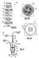
- FIG. 1Aillustrates an array of 64 individually addressable electrodes made in accordance with the present invention
- FIG. 1Billustrates an array of 66 individually addressable electrodes made in accordance with the present invention
- FIG. 2Ais a flow chart diagram describing the processes involved in fabricating individually addressable electrode arrays
- FIGS. 2A and 2Bare examples of masks for array fabrication
- FIG. 3is a sectional view of the electrochemical deposition head
- FIG. 4Ais a sectional view of the electrochemical cell
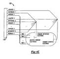
- FIG. 4Bis a sectional view of the cathode assembly associated with the electrochemical cell of FIG. 4A;
- FIG. 4Cis an exploded view of the anode assembly associated with the electrochemical cell of FIG. 4A;
- FIG. 4Dis a sectional view of the PCB interface associated with the anode assembly of FIG. 4C;
- FIG. 4Eis a circuit diagram showing the electrical connections in the PCB interface of FIG. 4D.
- FIG. 5is a graph illustrative of the relationship between electrode composition and associated activity for an example system synthesized and measured using embodiments of the present invention.
- the present inventioncomprises an electrochemical synthesis and testing system consisting of a number of separate parts including individually addressable electrode arrays, a fully automated deposition head, an electrochemical cell and its associated electronics, and a multi-channel potentiostat. These components provide a means for investigating complex multi-component systems, by giving a user the ability to rapidly synthesize and evaluate large numbers of diverse materials in short periods of time.
- the individually addressable electrode arrays 10 of the present inventionare illustrated in FIGS. 1A and 1B.
- the arrays 10consist of either sixty-four or sixty-six independent electrodes 12 (with areas of between 1 and 2 mm 2 ) that are fabricated on inert substrates 14 .
- Arrays with as little as 10 or as many as 100 electrodesmay be made in accordance with the methods provided in the present invention.
- Example substratesinclude, but are not limited to, glass, quartz, sapphire, alumina, plastics, or thermally treated silicon. Other suitable substrate materials will be readily apparent to those of skill in the art.
- the individual electrodes 12are located substantially in the center of the substrate 14 , and are connected to contact pads 13 around the periphery of the substrate with wires 16 .
- the electrodes 12 , associated wires 16 , and contact pads 13are fabricated from conducting materials (such as gold, silver, platinum, copper, or other commonly used electrode materials).
- conducting materialssuch as gold, silver, platinum, copper, or other commonly used electrode materials.
- the arraysare fabricated on standard 3′′ thermally oxidized single crystal silicon wafers, and the electrodes are gold with surface areas of about 1.26 mm 2.
- a patterned insulating layer 18covers the wires 16 and an inner portion of the peripheral contact pads 13 , but leaves the electrodes 12 and the outer portion of the peripheral contact pads 13 exposed (preferably approximately half of the contact pad 13 is covered with this insulating layer). Because of the insulating layer 18 , it is possible to connect a lead (e.g, an alligator clip) to the outer portion of a given contact pad 13 and address its associated electrode 12 while the array 10 is immersed in solution, without having to worry about reactions that can occur on the wires 16 or peripheral contact pads.
- a leade.g, an alligator clip
- the insulting layer 18may be, for example, glass, cilica (SiO 2 ), alumina (Al 2 O 3 ), magnesium oxide (MgO), silicon nitride (Si 3 N 4 ), boon nitride (BN), yttrium oxide (Y 2 O 3 ), titanium dioxide (TiO 2 ), hardened photoresist, or other suitable material known to be insulating in nature.
- photolithographic techniquescan be applied to design and fabricate electrode array patterns on it.
- photoresistBy applying a predetermined amount of photoresist to the substrate, photolyzing preselected regions of the photoresist, removing those regions that have been photolyzed (e.g., by using an appropriate developer), depositing one or more metals over the entire surface and removing predetermined regions of these metals (e.g., by dissolving the underlying photoresist), one can fabricate intricate patterns of individually addressable electrodes on the substrate.
- a cleaning step 22that comprises washing the wafer in a suitable solvent (such as methanol or isopropanol) followed by baking in a plasma cleaning oven
- a photoresist deposition step 24in which a first layer of photoresist is applied to the wafer is then done.
- a photoresist deposition step 24in which a first layer of photoresist is applied to the wafer is then done.
- the photoresistis applied to the wafer using a standard spin coating system (commonly used and familiar to those skilled in the art) which is set to leave a final thickness of between 1 and 2 ⁇ m on the wafer.
- the photoresistis then cured at a predetermined temperature for a predetermined time to condition the photoresist.
- the curing temperatureis between 90° C. and 130° C. and the curing time is between 30 sec and 2 minutes.
- a primary electrode mask 27is then placed over the wafer that is then photolyzed on a mask aligner system (commonly used and familiar to those skilled in the art). After exposure to ultraviolet (UV) light during the photolysis step 26 , regions 29 on the wafer are then dissolved away using an appropriate developing solution (e.g., Shipley Microposit MF-319 or equivalent). The wafer is then placed in a physical vapor deposition (PVD) system where a metals are deposited during a metal deposition step 28 .
- PVDphysical vapor deposition
- Example PVD systemsinclude: sputtering, electron beam evaporation and pulsed laser deposition.
- the metals deposited by the appropriate PVD systemconsist of an adhesion layer (such as Cr, Ta, or W) followed by the desired electrode material (such as Au, Ag Cu or Pt).
- the thicknesses of these layersmay vary substantially, but are typically 100-500 ⁇ for the adhesion layer and 1000-5000 ⁇ for the electrode layer.
- a second layer of photoresistis then deposited on the wafer during a second photoresist deposition step 32 , cured as described above, and photolyzed through an isolation mask 35 during a second photolysis step 34 .
- the aim of this second photolysis stepis to expose only the regions of the electrode pads 36 and an outer contact ring 38 , the exposed photoresist on which is dissolved away after the photolysis step.
- a final annealing step 40 at between 90° C. and 130° C. for between 1 minute and 10 (or more) minuteshardens the remaining photoresist into an effective insulating layer.
- an insulating layersuch as glass, silica, alumina, magnesium oxide, silicon nitride, boron nitride, yttrium oxide or titanium dioxide
- a suitable PVD techniqueafter photolysis of the second photoresist layer through an inverse isolation mask (the negative of the isolation mask 35 in FIG. 2 C).
- the arrays of the present inventionconsist of a plurality of individually addressable electrodes that are insulated from each other (by adequate spacing) and from the substrate (since they are fabricated on an insulating substrate), and whose interconnects are insulated from the electrochemical testing solution (by the hardened photoresist or other suitable insulating material).
- the number of electrodescan vary according to a desired number, but typically the arrays consist of 10 or more electrodes, 30 or more electrodes, and preferably more than 50 electrodes. In the embodiments shown in FIG. 1 A and FIG. 1B, more than 60 electrodes are in a single array. Materials are deposited on each of the individually addressable electrodes. Thus, an array of individually addressable materials is also a part of this invention, with the number of materials equaling the number of addressable electrodes. The materials in the array may be the same or different, as described below.
- the deposition of materials on the above described electrode arrays to make a library of an equal number of compositionsis accomplished by the electrodeposition of species from solution using standard electrochemical methods.
- the compositionsmay all be the same, or may be different from each other.
- the depositionsare carried out by immersing the electrode array in a standard electrochemical deposition chamber containing the array, a platinum mesh counter electrode, and a reference electrode (e.g., Ag/AgCl).
- the chamberis filled with a plating solution containing known amounts of source materials to be deposited.
- compositions depositedmay be obtained either by directly changing the solution composition for each deposition or by using different electrochemical deposition techniques, or both.
- Examples of how one may change the electrode composition by changing the deposition techniquecan include: changing the deposition potential, changing the length of the deposition time, varying the counter anions, using different concentrations of each species, and even using different electrochemical deposition programs (e.g., potentiostatic oxidation/reduction, galvanostatic oxidation/reduction, potential square-wave voltammetry, potential stair-step voltammetry, etc.).
- electrochemical deposition programse.g., potentiostatic oxidation/reduction, galvanostatic oxidation/reduction, potential square-wave voltammetry, potential stair-step voltammetry, etc.
- the deposition of materials on the electrode arrayis carried out using a partially or fully automated solution delivery/electroplating system consisting of a deposition head and its associated syringe pumps, robotics and electronics.
- the deposition head 50consists of a rod 52 that is tapered at the tip.
- the tapered end of the deposition headis wrapped with a mesh counter electrode 54 (e.g., Pt) that is connected to an external power supply (not shown) via a wire 56 that is embedded in the wall of the head.
- the deposition headhas a 1-3 mm ID which is tapered to ca. 1 mm ID at the tip.
- a solution delivery tube 58 containing an interannular reference electrode 60is located into the center of the rod 52 .
- the reference electrode 60may be a standard reference electrode (such as Ag/AgCl, SHE, SCE or Hg/HgSO 4 ) or a quasi-reference electrode (such as a piece of Pt wire).
- the reference electrode 60is split off from the solution delivery tube 58 and connected to an external power supply or potentiostat (not shown).
- the flow of liquids through the solution delivery tube 58is controlled by commercially available syringe pumps (not shown) that can precisely deliver volumes of liquids with accurate displacements in the ⁇ L/hour regime.
- the liquids that are dispensed from the aforementioned pumpsare either mixed prior to entering the solution delivery tube (via an external mixer) or via a frit 62 embedded in the deposition head.
- the deposition head 50is held over a given electrode pad 12 on an electrode array 10 by a clamp 68 that is connected to robotics (not shown) that can control its precise position.
- the ideal positionas illustrated in FIG. 3, is ca. 1-2 mm above the electrode pad 12 .
- the operation of the automated deposition systemis described as follows. After positioning the deposition head above a given electrode (sometimes referred to as the ‘working’ electrode), the syringe pumps are activated causing a predetermined mixture of liquids containing predetermined amounts of source materials to flow through the tube 58 at an exactly specified flow rate and collect in a region 70 surrounding a given electrode 12 . When the liquid contacts all three electrodes, a complete electric circuit is formed in this region. Coincident with the formation of this circuit, a predetermined potential is applied to the working electrode (via an external power supply or potentiostat) causing species present in the liquid above it to deposit on the electrode surface.
- a predetermined potentialis applied to the working electrode (via an external power supply or potentiostat) causing species present in the liquid above it to deposit on the electrode surface.
- the headis rinsed and moved to the next electrode where the next specified mixture is delivered and plated out.
- a deposition timeof between 1 and 2 minutes is used.
- the entire procedurecan take less than 3 minutes per deposition or about three hours per library of sixty-four to sixty-six elements.
- the cell 80comprises a cylindrical glass housing 82 (of approximate diameter equal to that of the wafers) that is sandwiched between two plastic end members 84 .
- the anode array assembly 86which holds the individually addressable electrode arrays 10 , is fit into one side of the cell, and the cathode assembly 95 , which holds a counter electrode 88 and its associated external wire coupling 96 , is fit into the other side.
- the cellis held together by four screw fasteners 90 which fit through holes 98 located on the corners of the end members 84 .
- a reference electrode compartment 92is bored into the glass housing to allow the insertion of a reference electrode (not shown).
- a liquid filling hole 94allows for the filling and drainage of testing solutions from the electrochemical cell.
- FIG. 4Can exploded view of the components of the anode assembly is shown.
- the glass housing 82 of the cellis fit over the inner flange 106 of a molded adapter 102 and is held in place against the adapter with an o-ring 100 .
- This o-ringprovides a water-tight seal for this part of the assembly.
- the diameter of the outer flange 104 of the adapter 102is the same as that of the glass housing, while that of the inner flange 106 is slightly smaller allowing one half of it to fit into the glass housing and the other half of it to fit into the remaining pieces of the anode assembly.
- a groove 108is cut into the lower lip of the adapter 102 .
- This grooveholds an o-ring 110 which makes a water-tight seal with the anode array 10 when the adapter is pressed against it.
- Electrical contact to the anode array 10is made using a ring of elastomeric contacts 114 which are pressed between the peripheral pads of the array (see FIGS. 1A-1B) and contact pads 122 on a printed circuit board (PCB) assembly 112 .
- These elastomeric contactscontain miniature wires encased in a flexible rubber sheath. They are commercially available and known to those skilled in the art.
- the anode array 10is affixed to a backing plate 116 and attached to the PCB 112 with screws (not shown) through holes 118 . This backing plate holds the electrode array and ensures contact between the peripheral pads on the wafer and the contacts on the PCB. This completes the anode assembly which is fitted together with screw fasteners 90 through holes 98 in end member 84 as shown in FIG. 4 A.
- the PCB 112consists of a rectangular plate 120 on which is deposited an intricate pattern of wires and connectors.
- the contact pads 122which provide electrical connection to peripheral pads on the anode array (FIGS. 1 A- 1 B), are routed to four high-density pin connectors 128 that provide a cable connection to an external power supply (not shown) or multi-channel potentiostat 132 .
- the multi-channel potentiostat 132is essentially a collection of individual potentiostats bundled together in a single unit. These individual potentiostats can precisely control the current or potential applied to each electrode in the system.
- a common reference electrode contact 124 and a common counter electrode contact 126are also wired to the high density pin connectors so that individual electrode pads on a given electrode array may be connected to the same reference and counter electrode during test measurements in the electrochemical cell.
- each individual electrode on a given anode arraycan be individually addressed (e.g., during a electrodeposition procedure).
- the PCB in connection with the electrochemical cell whip 80 (FIG. 4A) and multi-channel potentiostatall of the electrodes on the array may be simultaneously addressed (e.g., during a catalytic activity measurement). Such catalytic measurements can be made in a time fame of between 1 and 2 minutes for each array of materials.
- FIG. 4Da sixty-four contact pad configuration is shown. It should be understood that a sixty-six contact pad configuration would be needed for experiments using a sixty-six member electrode array (FIG. 1 B), and that PCB's having greater or less contact pads and associated connections are straightforward extensions of the concept and intended to be included within the scope of the present invention.
- the following exampleillustrates the electrochemical deposition and screening measurements for a very specific system using selected embodiments of the present invention. It is only one of the many possible uses of the present invention.
- the exampleillustrates how a library of sixty-four different Pt—Ru compositions may be prepared and tested for methanol oxidation activity. It should be understood that the solution and electrode compositions, types of reference and counter electrodes, applied and measured potentials, screening test conditions, and associated results are merely illustrative and that a person skilled in the art may make reasonable substitutions or modifications to these components without deviating from the spirit and scope of the invention.
- a binary Pt—Ru library containing sixty-four different Pt—Ru compositionswas synthesized on a sixty-four element individually addressable electrode array (gold electrodes) using the electrochemical reduction of acidic solutions containing mixtures of platinum chloride (H 2 PtCl 6 ) and ruthenium chloride (RuCl 3 ).
- the first working electrode on the arraywas held at a constant potential of ⁇ 0.25V (vs Ag/AgCl) for two minutes under constant stirring.
- the electrode arraywas then rotated in the deposition chamber and the solution composition adjusted (by the removal of a 5 ml aliquot of the RuCl 3 solution and its replacement with a 5 ml aliquot of a 0.01M H 2 PtCl 6 solution), where the next electrode was deposited at the same potential and for the same amount of time. This procedure was continued until all sixty-four electrodes were deposited with Pt—Ru compositions, whose thickness averaged between 1000-2000. Analysis (via X-ray fluorescence measurements) of the sixty-four electrodes showed a continuously varying gradient of Ru and Pt compositions among the sixty-four electrodes on the array.
- This Pt—Ru librarywas then screened for methanol oxidation activity by placing it into the electrochemical cell (described earlier) which was filled with a solution of 1.0M methanol in 0.5M H 2 SO 4 (a standard testing solution composition for studying the electrooxidation of methanol in fuel cells).
- the cellalso contained a Hg/HgSO 4 reference electrode and a Pt mesh counter electrode. Chronoamperometry measurements (i.e., holding a given electrode at a given potential and measuring the current that passes as a function of time) were then performed on all of the electrodes in the library by pulsing each individual electrode to a potential of ⁇ 0.125V (vs Hg/HgSO 4 ) and holding it there for 1 minute while monitoring and recording the current that passed. The results of this experiment are depicted in FIG. 5 .
- a three-dimensional plot 140 of electrode composition 142(expressed as mole fraction platinum) versus current 144 (in amps per square centimeter) versus time 146 (in seconds) is displayed.
- Individual electrodesare represented by their compositions along the x-axis, with their associated activities represented by their current values on the z-axis.
- the most active electrode compositions 150are centered around a 50:50 Pt:Ru electrode composition which agrees with results reported in the literature (e.g., D. Chu and S. Gilman, J. Electrochem. Soc . 1996, 143, 1685). Although the results plotted in FIG.
- Plating solutionscomprising one or more of the water soluble forms of the transition elements (e.g., Sc, Ti, V, Cr, Mn, Fe, Co, Ni, Cu, Zn, Y, Zr, Nb, Mo, Ru, Rh, Pd, Ag, Cd, Hf, Ta, W. Re, Os, Ir, Pt, Au, Hg) as well as many main group elements (e.g., Al, Ga, Ge, In, Sn, Sb, Te, Tl, Pb, Bi) can be used with the present invention, and will give rise to enormous variations in library compositions which can in turn be studied in an enormous variety of catalytic systems.
- transition elementse.g., Sc, Ti, V, Cr, Mn, Fe, Co, Ni, Cu, Zn, Y, Zr, Nb, Mo, Ru, Rh, Pd, Ag, Cd, Hf, Ta, W. Re, Os, Ir, Pt, Au, Hg
- main group elementse.g., Al
- the present inventionprovides a far superior method of electrochemically depositing and screening the properties of diverse materials.
- this inventionone can efficiently prepare libraries of varying elemental composition, and, since these libraries are prepared on individually addressable electrode arrays, one can also directly measure properties of these compositions.
Landscapes
- Chemical & Material Sciences (AREA)
- Engineering & Computer Science (AREA)
- Organic Chemistry (AREA)
- Nanotechnology (AREA)
- Chemical Kinetics & Catalysis (AREA)
- Physics & Mathematics (AREA)
- Composite Materials (AREA)
- Condensed Matter Physics & Semiconductors (AREA)
- General Physics & Mathematics (AREA)
- Materials Engineering (AREA)
- Crystallography & Structural Chemistry (AREA)
- Investigating Or Analyzing Materials By The Use Of Electric Means (AREA)
Abstract
Description
Claims (9)
Priority Applications (3)
| Application Number | Priority Date | Filing Date | Title |
|---|---|---|---|
| US09/694,176US6818110B1 (en) | 1997-09-30 | 2000-10-23 | Combinatorial electrochemical deposition and testing system |
| US10/106,722US20020100692A1 (en) | 1997-09-30 | 2002-03-26 | Combinatorial electrochemical deposition and testing system |
| US10/106,734US6756109B2 (en) | 1997-09-30 | 2002-03-26 | Combinatorial electrochemical deposition and testing system |
Applications Claiming Priority (3)
| Application Number | Priority Date | Filing Date | Title |
|---|---|---|---|
| US08/941,170US6468806B1 (en) | 1996-10-02 | 1997-09-30 | Potential masking systems and methods for combinatorial library synthesis |
| US09/119,187US6187164B1 (en) | 1997-09-30 | 1998-07-20 | Method for creating and testing a combinatorial array employing individually addressable electrodes |
| US09/694,176US6818110B1 (en) | 1997-09-30 | 2000-10-23 | Combinatorial electrochemical deposition and testing system |
Related Parent Applications (1)
| Application Number | Title | Priority Date | Filing Date |
|---|---|---|---|
| US09/119,187DivisionUS6187164B1 (en) | 1997-09-30 | 1998-07-20 | Method for creating and testing a combinatorial array employing individually addressable electrodes |
Related Child Applications (2)
| Application Number | Title | Priority Date | Filing Date |
|---|---|---|---|
| US10/106,722DivisionUS20020100692A1 (en) | 1997-09-30 | 2002-03-26 | Combinatorial electrochemical deposition and testing system |
| US10/106,734DivisionUS6756109B2 (en) | 1997-09-30 | 2002-03-26 | Combinatorial electrochemical deposition and testing system |
Publications (1)
| Publication Number | Publication Date |
|---|---|
| US6818110B1true US6818110B1 (en) | 2004-11-16 |
Family
ID=33422458
Family Applications (3)
| Application Number | Title | Priority Date | Filing Date |
|---|---|---|---|
| US09/694,176Expired - LifetimeUS6818110B1 (en) | 1997-09-30 | 2000-10-23 | Combinatorial electrochemical deposition and testing system |
| US10/106,734Expired - LifetimeUS6756109B2 (en) | 1997-09-30 | 2002-03-26 | Combinatorial electrochemical deposition and testing system |
| US10/106,722AbandonedUS20020100692A1 (en) | 1997-09-30 | 2002-03-26 | Combinatorial electrochemical deposition and testing system |
Family Applications After (2)
| Application Number | Title | Priority Date | Filing Date |
|---|---|---|---|
| US10/106,734Expired - LifetimeUS6756109B2 (en) | 1997-09-30 | 2002-03-26 | Combinatorial electrochemical deposition and testing system |
| US10/106,722AbandonedUS20020100692A1 (en) | 1997-09-30 | 2002-03-26 | Combinatorial electrochemical deposition and testing system |
Country Status (1)
| Country | Link |
|---|---|
| US (3) | US6818110B1 (en) |
Cited By (28)
| Publication number | Priority date | Publication date | Assignee | Title |
|---|---|---|---|---|
| US20060060301A1 (en)* | 2004-09-17 | 2006-03-23 | Lazovsky David E | Substrate processing using molecular self-assembly |
| US20060108320A1 (en)* | 2004-11-22 | 2006-05-25 | Lazovsky David E | Molecular self-assembly in substrate processing |
| FR2884318A1 (en)* | 2005-04-12 | 2006-10-13 | Univ Rennes I Etablissement Pu | ELECTROCHEMICAL VOLTAMETRIC ANALYSIS METHOD, ANALYSIS MEDIUM AND DEVICE FOR IMPLEMENTING IT. |
| US20060264020A1 (en)* | 2005-05-18 | 2006-11-23 | Intermolecular Inc. | Formation of a masking layer on a dielectric region to facilitate formation of a capping layer on electrically conductive regions separated by the dielectric region |
| US20060261434A1 (en)* | 2005-05-18 | 2006-11-23 | Intermolecular Inc. | Formation of a masking layer on a dielectric region to facilitate formation of a capping layer on electrically conductive regions separated by the dielectric region |
| US20060292845A1 (en)* | 2004-09-17 | 2006-12-28 | Chiang Tony P | Processing substrates using site-isolated processing |
| US20060292846A1 (en)* | 2004-09-17 | 2006-12-28 | Pinto Gustavo A | Material management in substrate processing |
| US20070068819A1 (en)* | 2005-05-25 | 2007-03-29 | Saravjeet Singh | Electroplating apparatus based on an array of anodes |
| US20070082485A1 (en)* | 2005-10-11 | 2007-04-12 | Chiang Tony P | Methods for discretized formation of masking and capping layers on a substrate |
| US20070082508A1 (en)* | 2005-10-11 | 2007-04-12 | Chiang Tony P | Methods for discretized processing and process sequence integration of regions of a substrate |
| US20070089857A1 (en)* | 2005-10-11 | 2007-04-26 | Chiang Tony P | Systems for discretized processing of regions of a substrate |
| US20070138005A1 (en)* | 2005-12-20 | 2007-06-21 | Feng Chia University | Electrochemical testing device |
| US20070166989A1 (en)* | 2005-05-18 | 2007-07-19 | Intermolecular, Inc. | Substrate processing including a masking layer |
| US20070202610A1 (en)* | 2006-02-10 | 2007-08-30 | Chiang Tony P | Method and apparatus for combinatorially varying materials, unit process and process sequence |
| US20070199510A1 (en)* | 2006-02-24 | 2007-08-30 | Weiner Kurt H | Systems and methods for sealing in site-isolated reactors |
| US20070261958A1 (en)* | 2006-05-09 | 2007-11-15 | U.S.A. As Represented By The Secretary Of The Army | Electrochemical test apparatus and method for its use |
| US20070267631A1 (en)* | 2006-05-18 | 2007-11-22 | Intermolecular, Inc. | System and Method for Increasing Productivity of Combinatorial Screening |
| US20080156769A1 (en)* | 2006-12-29 | 2008-07-03 | Intermolecular, Inc. | Advanced mixing system for integrated tool having site-isolated reactors |
| US20080312090A1 (en)* | 2007-06-14 | 2008-12-18 | Zachary Fresco | Combinatorial Processing Including Stirring |
| US20090047881A1 (en)* | 2007-08-14 | 2009-02-19 | Peter Satitpunwaycha | Combinatorial processing including rotation and movement within a region |
| US20090155476A1 (en)* | 2007-12-18 | 2009-06-18 | Aaron Francis | Vented Combinatorial Processing Cell |
| US7670465B2 (en) | 2002-07-24 | 2010-03-02 | Applied Materials, Inc. | Anolyte for copper plating |
| JP2013039559A (en)* | 2011-08-11 | 2013-02-28 | Eppendorf Ag | Laboratory sample instrument with printed circuit board cable device |
| US20150041328A1 (en)* | 2013-08-07 | 2015-02-12 | Xagenic Inc. | Sensor growth controller |
| US9207515B2 (en) | 2013-03-15 | 2015-12-08 | Ashwin-Ushas Corporation, Inc. | Variable-emittance electrochromic devices and methods of preparing the same |
| US9274395B2 (en) | 2011-11-15 | 2016-03-01 | Ashwin-Ushas Corporation, Inc. | Complimentary polymer electrochromic device |
| US9482880B1 (en) | 2015-09-15 | 2016-11-01 | Ashwin-Ushas Corporation, Inc. | Electrochromic eyewear |
| US9632059B2 (en) | 2015-09-03 | 2017-04-25 | Ashwin-Ushas Corporation, Inc. | Potentiostat/galvanostat with digital interface |
Families Citing this family (28)
| Publication number | Priority date | Publication date | Assignee | Title |
|---|---|---|---|---|
| US20030224387A1 (en)* | 2002-05-22 | 2003-12-04 | Sandeep Kunwar | Association of molecules with electrodes of an array of electrodes |
| US20040099531A1 (en)* | 2002-08-15 | 2004-05-27 | Rengaswamy Srinivasan | Methods and apparatus for electrochemically testing samples for constituents |
| KR100545192B1 (en)* | 2003-06-19 | 2006-01-24 | 동부아남반도체 주식회사 | Deposition stop time detection device and copper wiring formation method of semiconductor device using same |
| JP4206900B2 (en)* | 2003-10-27 | 2009-01-14 | ソニー株式会社 | Bioassay substrate with extended power supply wiring |
| US7069203B2 (en)* | 2003-10-31 | 2006-06-27 | Chevron Oronite Company Llc | Method and system of product development process for chemical compositions using high volume modeling |
| US7462490B2 (en) | 2003-10-31 | 2008-12-09 | Chevron Oronite Company Llc | Combinatorial lubricating oil composition libraries |
| US20050095717A1 (en)* | 2003-10-31 | 2005-05-05 | Wollenberg Robert H. | High throughput screening methods for lubricating oil compositions |
| US7150182B2 (en)* | 2003-10-31 | 2006-12-19 | Chevron Oronite Company, Llc | High throughput screening methods for lubricating oil compositions |
| US7579192B2 (en) | 2003-10-31 | 2009-08-25 | Chevron Oronite Company Llc | High throughput screening methods for lubricating oil compositions |
| US20050095714A1 (en) | 2003-10-31 | 2005-05-05 | Wollenberg Robert H. | High throughput preparation of lubricating oil compositions for combinatorial libraries |
| JP4285206B2 (en)* | 2003-11-11 | 2009-06-24 | ソニー株式会社 | Bioassay substrate with extended power supply wiring |
| US8249816B2 (en)* | 2004-02-13 | 2012-08-21 | Chevron Oronite Company, Llc | High throughput screening methods for fuel compositions |
| US7985592B2 (en)* | 2004-02-13 | 2011-07-26 | Chevron Oronite Company Llc | High throughput screening methods for lubricating oil compositions |
| US7306948B2 (en)* | 2004-02-13 | 2007-12-11 | Chevron Oronite Company Llc | High throughput screening methods for lubricating oil compositions |
| US7137289B2 (en) | 2004-02-13 | 2006-11-21 | Chevron Oronite Company, Llc | High throughput screening methods for lubricating oil compositions |
| US7747402B2 (en)* | 2005-02-11 | 2010-06-29 | Dionex Corporation | Method, system and software application for electrochemical analysis |
| US7655126B2 (en)* | 2006-03-27 | 2010-02-02 | Federal Mogul World Wide, Inc. | Fabrication of topical stopper on MLS gasket by active matrix electrochemical deposition |
| EP1894703A1 (en)* | 2006-08-28 | 2008-03-05 | Curt G. Joa, Inc. | Bonding method for continuous traveling web |
| US8366894B2 (en)* | 2009-02-20 | 2013-02-05 | Giner, Inc. | Multi-gas microsensor assembly |
| WO2014134659A1 (en)* | 2013-03-08 | 2014-09-12 | Monash University | Pools of liquid electrode tester |
| WO2015192010A1 (en)* | 2014-06-13 | 2015-12-17 | Wafergen, Inc. | Systems for single or multiple cell counting and dispensing |
| WO2017081669A1 (en) | 2015-11-13 | 2017-05-18 | North-West University | Combinatorial screening array |
| WO2017081587A1 (en) | 2015-11-13 | 2017-05-18 | North-West University | Electrocatalyst for the reduction of oxygen |
| WO2017087884A1 (en)* | 2015-11-19 | 2017-05-26 | Fabric8Labs, Inc. | Three dimensional additive manufacturing of metal objects by stereo-electrochemical deposition |
| WO2020075173A1 (en)* | 2018-10-11 | 2020-04-16 | Ramot At Tel-Aviv University Ltd. | Meniscus-confined three-dimensional electrodeposition |
| CN110708905A (en)* | 2019-09-29 | 2020-01-17 | 联想(北京)有限公司 | Shell, manufacturing method of shell and electronic equipment |
| CN116473551B (en)* | 2023-06-19 | 2023-08-29 | 中南大学 | Blood ion concentration sensor chip and detection device based on hollow microneedle array |
| CN118362496B (en)* | 2024-05-15 | 2024-12-27 | 中国石油大学(华东) | A detachable array electrode electrochemical experimental system and its testing method |
Citations (33)
| Publication number | Priority date | Publication date | Assignee | Title |
|---|---|---|---|---|
| US4082619A (en) | 1976-01-07 | 1978-04-04 | Heinz Dehnert | Method of forming a comb-like electrode structure |
| US4155815A (en) | 1978-04-03 | 1979-05-22 | Francis William L | Method of continuous electroplating and continuous electroplating machine for printed circuit board terminals |
| US4539932A (en) | 1983-04-01 | 1985-09-10 | General Motors Corporation | Robot painting system for automobiles |
| US4689246A (en) | 1984-10-26 | 1987-08-25 | Itek Corporation | Method of fabricating a PbS-PbSe IR detector array |
| US4871435A (en) | 1988-10-14 | 1989-10-03 | Charles Denofrio | Electroplating apparatus |
| US5093874A (en) | 1991-04-01 | 1992-03-03 | Eastman Kodak Company | Integrated electro-optical scanner with photoconductive substrate |
| US5100524A (en) | 1988-02-03 | 1992-03-31 | The General Electric Company, P.L.C. | Apparatus for selectively coating part of a member |
| US5345213A (en) | 1992-10-26 | 1994-09-06 | The United States Of America, As Represented By The Secretary Of Commerce | Temperature-controlled, micromachined arrays for chemical sensor fabrication and operation |
| US5356756A (en) | 1992-10-26 | 1994-10-18 | The United States Of America As Represented By The Secretary Of Commerce | Application of microsubstrates for materials processing |
| US5421987A (en) | 1993-08-30 | 1995-06-06 | Tzanavaras; George | Precision high rate electroplating cell and method |
| US5427674A (en) | 1991-02-20 | 1995-06-27 | Cinram, Ltd. | Apparatus and method for electroplating |
| US5441619A (en) | 1992-12-07 | 1995-08-15 | Ebara-Udylite Co., Ltd. | Electroplating apparatus |
| US5487824A (en) | 1993-08-31 | 1996-01-30 | Uemura Kogyo Kabushiki Kaisha | Electroplating apparatus and electroplating method of small articles |
| US5496463A (en) | 1993-12-08 | 1996-03-05 | Nihon Parkerizing Co., Ltd. | Process and apparatus for composite electroplating a metallic material |
| WO1996011878A1 (en) | 1994-10-18 | 1996-04-25 | The Regents Of The University Of California | The combinatorial synthesis of novel materials |
| US5556530A (en) | 1995-06-05 | 1996-09-17 | Walter J. Finklestein | Flat panel display having improved electrode array |
| US5640047A (en) | 1995-09-25 | 1997-06-17 | Mitsui High-Tec, Inc. | Ball grid assembly type semiconductor device having a heat diffusion function and an electric and magnetic shielding function |
| US5641391A (en) | 1995-05-15 | 1997-06-24 | Hunter; Ian W. | Three dimensional microfabrication by localized electrodeposition and etching |
| US5656139A (en) | 1995-02-13 | 1997-08-12 | International Business Machines Corporation | Electroplating apparatus |
| US5660699A (en) | 1995-02-20 | 1997-08-26 | Kao Corporation | Electroplating apparatus |
| US5667667A (en) | 1992-04-24 | 1997-09-16 | Isis Innovation Limited | Electrochemical treatment of surfaces |
| US5672256A (en)* | 1994-12-08 | 1997-09-30 | Lg Semicon Co., Ltd. | Multi-electrode biosensor and system and method for manufacturing same |
| US5695833A (en) | 1996-06-12 | 1997-12-09 | Bok; Hendrik F. | Method for uniform film coating of substrates |
| US5755948A (en) | 1997-01-23 | 1998-05-26 | Hardwood Line Manufacturing Co. | Electroplating system and process |
| US5786239A (en) | 1995-09-20 | 1998-07-28 | Sony Corporation | Method of manufacturing a semiconductor package |
| US5955028A (en)* | 1996-08-02 | 1999-09-21 | Caliper Technologies Corp. | Analytical system and method |
| US6132683A (en) | 1998-12-23 | 2000-10-17 | Matsushita Electric Industrial Co., Ltd. | Cell potential measuring electrode and measuring apparatus using the same |
| US6187164B1 (en) | 1997-09-30 | 2001-02-13 | Symyx Technologies, Inc. | Method for creating and testing a combinatorial array employing individually addressable electrodes |
| US6211576B1 (en) | 1998-09-18 | 2001-04-03 | Hitachi, Ltd. | Semiconductor device |
| US6306348B1 (en) | 1993-11-01 | 2001-10-23 | Nanogen, Inc. | Inorganic permeation layer for micro-electric device |
| US6468806B1 (en) | 1996-10-02 | 2002-10-22 | Symyx Technologies, Inc. | Potential masking systems and methods for combinatorial library synthesis |
| US6656826B2 (en) | 2000-09-27 | 2003-12-02 | Kabushiki Kaisha Toshiba | Semiconductor device with fuse to be blown with energy beam and method of manufacturing the semiconductor device |
| US6664138B2 (en) | 2001-06-19 | 2003-12-16 | Sanyo Electric Co., Ltd. | Method for fabricating a circuit device |
Family Cites Families (4)
| Publication number | Priority date | Publication date | Assignee | Title |
|---|---|---|---|---|
| US4225410A (en)* | 1978-12-04 | 1980-09-30 | Technicon Instruments Corporation | Integrated array of electrochemical sensors |
| US4628463A (en)* | 1984-03-05 | 1986-12-09 | Georgia Tech. Research Institute | Rapid-sweep electrochemical detector for chemical analysis of flow streams |
| US4927502A (en)* | 1989-01-31 | 1990-05-22 | Board Of Regents, The University Of Texas | Methods and apparatus using galvanic immunoelectrodes |
| US5120421A (en)* | 1990-08-31 | 1992-06-09 | The United States Of America As Represented By The United States Department Of Energy | Electrochemical sensor/detector system and method |
- 2000
- 2000-10-23USUS09/694,176patent/US6818110B1/ennot_activeExpired - Lifetime
- 2002
- 2002-03-26USUS10/106,734patent/US6756109B2/ennot_activeExpired - Lifetime
- 2002-03-26USUS10/106,722patent/US20020100692A1/ennot_activeAbandoned
Patent Citations (33)
| Publication number | Priority date | Publication date | Assignee | Title |
|---|---|---|---|---|
| US4082619A (en) | 1976-01-07 | 1978-04-04 | Heinz Dehnert | Method of forming a comb-like electrode structure |
| US4155815A (en) | 1978-04-03 | 1979-05-22 | Francis William L | Method of continuous electroplating and continuous electroplating machine for printed circuit board terminals |
| US4539932A (en) | 1983-04-01 | 1985-09-10 | General Motors Corporation | Robot painting system for automobiles |
| US4689246A (en) | 1984-10-26 | 1987-08-25 | Itek Corporation | Method of fabricating a PbS-PbSe IR detector array |
| US5100524A (en) | 1988-02-03 | 1992-03-31 | The General Electric Company, P.L.C. | Apparatus for selectively coating part of a member |
| US4871435A (en) | 1988-10-14 | 1989-10-03 | Charles Denofrio | Electroplating apparatus |
| US5427674A (en) | 1991-02-20 | 1995-06-27 | Cinram, Ltd. | Apparatus and method for electroplating |
| US5093874A (en) | 1991-04-01 | 1992-03-03 | Eastman Kodak Company | Integrated electro-optical scanner with photoconductive substrate |
| US5667667A (en) | 1992-04-24 | 1997-09-16 | Isis Innovation Limited | Electrochemical treatment of surfaces |
| US5345213A (en) | 1992-10-26 | 1994-09-06 | The United States Of America, As Represented By The Secretary Of Commerce | Temperature-controlled, micromachined arrays for chemical sensor fabrication and operation |
| US5356756A (en) | 1992-10-26 | 1994-10-18 | The United States Of America As Represented By The Secretary Of Commerce | Application of microsubstrates for materials processing |
| US5441619A (en) | 1992-12-07 | 1995-08-15 | Ebara-Udylite Co., Ltd. | Electroplating apparatus |
| US5421987A (en) | 1993-08-30 | 1995-06-06 | Tzanavaras; George | Precision high rate electroplating cell and method |
| US5487824A (en) | 1993-08-31 | 1996-01-30 | Uemura Kogyo Kabushiki Kaisha | Electroplating apparatus and electroplating method of small articles |
| US6306348B1 (en) | 1993-11-01 | 2001-10-23 | Nanogen, Inc. | Inorganic permeation layer for micro-electric device |
| US5496463A (en) | 1993-12-08 | 1996-03-05 | Nihon Parkerizing Co., Ltd. | Process and apparatus for composite electroplating a metallic material |
| WO1996011878A1 (en) | 1994-10-18 | 1996-04-25 | The Regents Of The University Of California | The combinatorial synthesis of novel materials |
| US5672256A (en)* | 1994-12-08 | 1997-09-30 | Lg Semicon Co., Ltd. | Multi-electrode biosensor and system and method for manufacturing same |
| US5656139A (en) | 1995-02-13 | 1997-08-12 | International Business Machines Corporation | Electroplating apparatus |
| US5660699A (en) | 1995-02-20 | 1997-08-26 | Kao Corporation | Electroplating apparatus |
| US5641391A (en) | 1995-05-15 | 1997-06-24 | Hunter; Ian W. | Three dimensional microfabrication by localized electrodeposition and etching |
| US5556530A (en) | 1995-06-05 | 1996-09-17 | Walter J. Finklestein | Flat panel display having improved electrode array |
| US5786239A (en) | 1995-09-20 | 1998-07-28 | Sony Corporation | Method of manufacturing a semiconductor package |
| US5640047A (en) | 1995-09-25 | 1997-06-17 | Mitsui High-Tec, Inc. | Ball grid assembly type semiconductor device having a heat diffusion function and an electric and magnetic shielding function |
| US5695833A (en) | 1996-06-12 | 1997-12-09 | Bok; Hendrik F. | Method for uniform film coating of substrates |
| US5955028A (en)* | 1996-08-02 | 1999-09-21 | Caliper Technologies Corp. | Analytical system and method |
| US6468806B1 (en) | 1996-10-02 | 2002-10-22 | Symyx Technologies, Inc. | Potential masking systems and methods for combinatorial library synthesis |
| US5755948A (en) | 1997-01-23 | 1998-05-26 | Hardwood Line Manufacturing Co. | Electroplating system and process |
| US6187164B1 (en) | 1997-09-30 | 2001-02-13 | Symyx Technologies, Inc. | Method for creating and testing a combinatorial array employing individually addressable electrodes |
| US6211576B1 (en) | 1998-09-18 | 2001-04-03 | Hitachi, Ltd. | Semiconductor device |
| US6132683A (en) | 1998-12-23 | 2000-10-17 | Matsushita Electric Industrial Co., Ltd. | Cell potential measuring electrode and measuring apparatus using the same |
| US6656826B2 (en) | 2000-09-27 | 2003-12-02 | Kabushiki Kaisha Toshiba | Semiconductor device with fuse to be blown with energy beam and method of manufacturing the semiconductor device |
| US6664138B2 (en) | 2001-06-19 | 2003-12-16 | Sanyo Electric Co., Ltd. | Method for fabricating a circuit device |
Non-Patent Citations (4)
| Title |
|---|
| Chu, Deryn, et al. J. Electrochem. Soc., vol. 143, No. 5, pp. 1685-1690, (1996). |
| Commonly Owned Co-pending Ser. No. 08/941,170. |
| Reddington, Erik; Sapienza, Anthony; Gurau, Bogdan; Viswanathan, Rameshkrishnan; Sarangapani, S.; Smotkin, Eugene S.; Mallouk, Thomas E., Combinatorial Electrochemistry: A Highly Parallel, Optical Screening Method for Discovery of Better Electrocatalysts, SCIENCE, vol. 280, pp. 1935-1937 (Jun. 12, 1998). |
| Richarz, Frank, et al. "Surface and electrochemical characterization of electrodeposited PtRu alloys," Surface Science, vol. 335, pp. 361-371, (1995). |
Cited By (57)
| Publication number | Priority date | Publication date | Assignee | Title |
|---|---|---|---|---|
| US7670465B2 (en) | 2002-07-24 | 2010-03-02 | Applied Materials, Inc. | Anolyte for copper plating |
| US20060292845A1 (en)* | 2004-09-17 | 2006-12-28 | Chiang Tony P | Processing substrates using site-isolated processing |
| US8882914B2 (en) | 2004-09-17 | 2014-11-11 | Intermolecular, Inc. | Processing substrates using site-isolated processing |
| US20060060301A1 (en)* | 2004-09-17 | 2006-03-23 | Lazovsky David E | Substrate processing using molecular self-assembly |
| US20060292846A1 (en)* | 2004-09-17 | 2006-12-28 | Pinto Gustavo A | Material management in substrate processing |
| US7309658B2 (en) | 2004-11-22 | 2007-12-18 | Intermolecular, Inc. | Molecular self-assembly in substrate processing |
| US20060108320A1 (en)* | 2004-11-22 | 2006-05-25 | Lazovsky David E | Molecular self-assembly in substrate processing |
| WO2006108759A1 (en)* | 2005-04-12 | 2006-10-19 | Universite De Rennes 1 | Method for voltametric electrochemical analysis and implementing device therefor |
| US20080190782A1 (en)* | 2005-04-12 | 2008-08-14 | Olivier Lavastre | Method for Voltametruc Electrochemical Analysis and Implementing Device Therefor |
| FR2884318A1 (en)* | 2005-04-12 | 2006-10-13 | Univ Rennes I Etablissement Pu | ELECTROCHEMICAL VOLTAMETRIC ANALYSIS METHOD, ANALYSIS MEDIUM AND DEVICE FOR IMPLEMENTING IT. |
| US7879710B2 (en) | 2005-05-18 | 2011-02-01 | Intermolecular, Inc. | Substrate processing including a masking layer |
| US20060261434A1 (en)* | 2005-05-18 | 2006-11-23 | Intermolecular Inc. | Formation of a masking layer on a dielectric region to facilitate formation of a capping layer on electrically conductive regions separated by the dielectric region |
| US20070166989A1 (en)* | 2005-05-18 | 2007-07-19 | Intermolecular, Inc. | Substrate processing including a masking layer |
| US20080246150A1 (en)* | 2005-05-18 | 2008-10-09 | Lazovsky David E | Formation of a masking layer on a dielectric region to facilitate formation of a capping layer on electrically conductive regions separated by the dielectric region |
| US20060264020A1 (en)* | 2005-05-18 | 2006-11-23 | Intermolecular Inc. | Formation of a masking layer on a dielectric region to facilitate formation of a capping layer on electrically conductive regions separated by the dielectric region |
| US8030772B2 (en) | 2005-05-18 | 2011-10-04 | Intermolecular, Inc. | Formation of a masking layer on a dielectric region to facilitate formation of a capping layer on electrically conductive regions separated by the dielectric region |
| US7749881B2 (en) | 2005-05-18 | 2010-07-06 | Intermolecular, Inc. | Formation of a masking layer on a dielectric region to facilitate formation of a capping layer on electrically conductive regions separated by the dielectric region |
| US7390739B2 (en) | 2005-05-18 | 2008-06-24 | Lazovsky David E | Formation of a masking layer on a dielectric region to facilitate formation of a capping layer on electrically conductive regions separated by the dielectric region |
| US7935240B2 (en) | 2005-05-25 | 2011-05-03 | Applied Materials, Inc. | Electroplating apparatus and method based on an array of anodes |
| US20110198229A1 (en)* | 2005-05-25 | 2011-08-18 | Applied Materials, Inc. | Electroplating apparatus based on an array of anodes |
| US20070068819A1 (en)* | 2005-05-25 | 2007-03-29 | Saravjeet Singh | Electroplating apparatus based on an array of anodes |
| TWI414639B (en)* | 2005-05-25 | 2013-11-11 | Applied Materials Inc | Electroplating apparatus based on an array of anodes |
| WO2006127320A3 (en)* | 2005-05-25 | 2007-11-22 | Applied Materials Inc | Electroplating apparatus based on an array of anodes |
| US20070089857A1 (en)* | 2005-10-11 | 2007-04-26 | Chiang Tony P | Systems for discretized processing of regions of a substrate |
| US8084400B2 (en) | 2005-10-11 | 2011-12-27 | Intermolecular, Inc. | Methods for discretized processing and process sequence integration of regions of a substrate |
| US8776717B2 (en) | 2005-10-11 | 2014-07-15 | Intermolecular, Inc. | Systems for discretized processing of regions of a substrate |
| US20070082508A1 (en)* | 2005-10-11 | 2007-04-12 | Chiang Tony P | Methods for discretized processing and process sequence integration of regions of a substrate |
| US7902063B2 (en) | 2005-10-11 | 2011-03-08 | Intermolecular, Inc. | Methods for discretized formation of masking and capping layers on a substrate |
| US7544574B2 (en) | 2005-10-11 | 2009-06-09 | Intermolecular, Inc. | Methods for discretized processing of regions of a substrate |
| US20070082487A1 (en)* | 2005-10-11 | 2007-04-12 | Chiang Tony P | Methods for discretized processing of regions of a substrate |
| US20070082485A1 (en)* | 2005-10-11 | 2007-04-12 | Chiang Tony P | Methods for discretized formation of masking and capping layers on a substrate |
| US20070138005A1 (en)* | 2005-12-20 | 2007-06-21 | Feng Chia University | Electrochemical testing device |
| US20070202610A1 (en)* | 2006-02-10 | 2007-08-30 | Chiang Tony P | Method and apparatus for combinatorially varying materials, unit process and process sequence |
| US20070202614A1 (en)* | 2006-02-10 | 2007-08-30 | Chiang Tony P | Method and apparatus for combinatorially varying materials, unit process and process sequence |
| US20070199510A1 (en)* | 2006-02-24 | 2007-08-30 | Weiner Kurt H | Systems and methods for sealing in site-isolated reactors |
| US7955436B2 (en) | 2006-02-24 | 2011-06-07 | Intermolecular, Inc. | Systems and methods for sealing in site-isolated reactors |
| US20070261958A1 (en)* | 2006-05-09 | 2007-11-15 | U.S.A. As Represented By The Secretary Of The Army | Electrochemical test apparatus and method for its use |
| US7695601B2 (en) | 2006-05-09 | 2010-04-13 | The United States Of America As Represented By The Secretary Of The Army | Electrochemical test apparatus and method for its use |
| US8772772B2 (en)* | 2006-05-18 | 2014-07-08 | Intermolecular, Inc. | System and method for increasing productivity of combinatorial screening |
| US20070267631A1 (en)* | 2006-05-18 | 2007-11-22 | Intermolecular, Inc. | System and Method for Increasing Productivity of Combinatorial Screening |
| US20080156769A1 (en)* | 2006-12-29 | 2008-07-03 | Intermolecular, Inc. | Advanced mixing system for integrated tool having site-isolated reactors |
| US8011317B2 (en) | 2006-12-29 | 2011-09-06 | Intermolecular, Inc. | Advanced mixing system for integrated tool having site-isolated reactors |
| US7960313B2 (en) | 2007-06-14 | 2011-06-14 | Intermolecular, Inc. | Combinatorial processing including stirring |
| US20080312090A1 (en)* | 2007-06-14 | 2008-12-18 | Zachary Fresco | Combinatorial Processing Including Stirring |
| US7785172B2 (en) | 2007-08-14 | 2010-08-31 | Intermolecular, Inc. | Combinatorial processing including rotation and movement within a region |
| US20090047881A1 (en)* | 2007-08-14 | 2009-02-19 | Peter Satitpunwaycha | Combinatorial processing including rotation and movement within a region |
| US9044774B2 (en) | 2007-12-18 | 2015-06-02 | Intermolecular, Inc. | Vented combinatorial processing cell |
| US20090155476A1 (en)* | 2007-12-18 | 2009-06-18 | Aaron Francis | Vented Combinatorial Processing Cell |
| JP2013039559A (en)* | 2011-08-11 | 2013-02-28 | Eppendorf Ag | Laboratory sample instrument with printed circuit board cable device |
| US9274395B2 (en) | 2011-11-15 | 2016-03-01 | Ashwin-Ushas Corporation, Inc. | Complimentary polymer electrochromic device |
| US9594284B2 (en) | 2011-11-15 | 2017-03-14 | Ashwin-Ushas Corporation, Inc. | Complimentary polymer electrochromic device |
| US10197881B2 (en) | 2011-11-15 | 2019-02-05 | Ashwin-Ushas Corporation, Inc. | Complimentary polymer electrochromic device |
| US9207515B2 (en) | 2013-03-15 | 2015-12-08 | Ashwin-Ushas Corporation, Inc. | Variable-emittance electrochromic devices and methods of preparing the same |
| US20150041328A1 (en)* | 2013-08-07 | 2015-02-12 | Xagenic Inc. | Sensor growth controller |
| US9632059B2 (en) | 2015-09-03 | 2017-04-25 | Ashwin-Ushas Corporation, Inc. | Potentiostat/galvanostat with digital interface |
| US9482880B1 (en) | 2015-09-15 | 2016-11-01 | Ashwin-Ushas Corporation, Inc. | Electrochromic eyewear |
| US10444544B2 (en) | 2015-09-15 | 2019-10-15 | Ashwin-Ushas Corporation | Electrochromic eyewear |
Also Published As
| Publication number | Publication date |
|---|---|
| US20020098332A1 (en) | 2002-07-25 |
| US20020100692A1 (en) | 2002-08-01 |
| US6756109B2 (en) | 2004-06-29 |
Similar Documents
| Publication | Publication Date | Title |
|---|---|---|
| US6818110B1 (en) | Combinatorial electrochemical deposition and testing system | |
| US6187164B1 (en) | Method for creating and testing a combinatorial array employing individually addressable electrodes | |
| US6937002B2 (en) | Method of using an array of electrodes for high throughput development and testing of materials | |
| US6592737B1 (en) | Method and apparatus for determination of additives in metal plating baths | |
| Bruckenstein et al. | Potential dependence of lead and silver underpotential coverages in acetonitrile using a piezoelectric crystal oscillator method | |
| US20030070917A1 (en) | Synthesis and characterization of materials for electrochemical cells | |
| EP1203950B1 (en) | Plating bath analysis | |
| WO1998014641A1 (en) | Potential masking systems and methods for combinatorial library synthesis | |
| Ciszkowska et al. | Preparation of a mercury disk microelectrode based on solid silver amalgam | |
| Ufheil et al. | Nanostructuring and nanoanalysis by scanning electrochemical microscopy (SECM) | |
| US6468410B1 (en) | Method for synthesis and characterization of electrode materials | |
| US6962649B2 (en) | Contact assemblies, methods for making contact assemblies, and machines with contact assemblies for electrochemical processing of microelectronic workpieces | |
| AU613135B2 (en) | Electrochemical electrodes | |
| US6118280A (en) | Method for detecting defects in dielectric film | |
| KR20040092446A (en) | Improved bath analysis | |
| KR20230134415A (en) | Electrochemical assembly to form semiconductor features | |
| Bond et al. | A survey of electrodes used for voltammetric analysis | |
| US20040099532A1 (en) | Apparatus and method for controlling plating uniformity | |
| US7294243B2 (en) | Contact assemblies for electrochemical processing of microelectronic workpieces and method of making thereof | |
| KR200347745Y1 (en) | Noble metal contacts for plating applications | |
| US6949172B1 (en) | Arrangement enabling a liquid to flow evenly around a surface of a sample and use of said arrangement | |
| US6758955B2 (en) | Methods for determination of additive concentration in metal plating baths | |
| US20020112970A1 (en) | Automated chemical management system having improved analysis unit | |
| CN114002285A (en) | A kind of polyaniline-nano-bismuth composite electrode for heavy metal detection and preparation method thereof | |
| US20130331296A1 (en) | Method and System for Combinatorial Electroplating and Characterization |
Legal Events
| Date | Code | Title | Description |
|---|---|---|---|
| FEPP | Fee payment procedure | Free format text:PAYOR NUMBER ASSIGNED (ORIGINAL EVENT CODE: ASPN); ENTITY STATUS OF PATENT OWNER: LARGE ENTITY | |
| AS | Assignment | Owner name:SYMYX TECHNOLOGIES, INC., CALIFORNIA Free format text:ASSIGNMENT OF ASSIGNORS INTEREST;ASSIGNORS:WARREN, CHRISTOPHER JR.;HAUSHALTER, ROBERT C.;MATSIEV, LEONID;AND OTHERS;REEL/FRAME:015090/0369;SIGNING DATES FROM 19980716 TO 20001020 | |
| STCF | Information on status: patent grant | Free format text:PATENTED CASE | |
| FPAY | Fee payment | Year of fee payment:4 | |
| AS | Assignment | Owner name:SYMYX SOLUTIONS, INC., CALIFORNIA Free format text:ASSIGNMENT OF ASSIGNORS INTEREST;ASSIGNOR:SYMYX TECHNOLOGIES, INC.;REEL/FRAME:022939/0564 Effective date:20090701 Owner name:SYMYX SOLUTIONS, INC.,CALIFORNIA Free format text:ASSIGNMENT OF ASSIGNORS INTEREST;ASSIGNOR:SYMYX TECHNOLOGIES, INC.;REEL/FRAME:022939/0564 Effective date:20090701 | |
| FEPP | Fee payment procedure | Free format text:PAYOR NUMBER ASSIGNED (ORIGINAL EVENT CODE: ASPN); ENTITY STATUS OF PATENT OWNER: LARGE ENTITY Free format text:PAYER NUMBER DE-ASSIGNED (ORIGINAL EVENT CODE: RMPN); ENTITY STATUS OF PATENT OWNER: LARGE ENTITY | |
| FPAY | Fee payment | Year of fee payment:8 | |
| AS | Assignment | Owner name:INTERMOLECULAR, INC., CALIFORNIA Free format text:ASSIGNMENT OF ASSIGNORS INTEREST;ASSIGNORS:SYMYX TECHNOLOGIES, INC.;SYMYX SOLUTIONS, INC.;REEL/FRAME:035311/0356 Effective date:20111123 | |
| FPAY | Fee payment | Year of fee payment:12 |