US6817903B1 - Process for reducing leakage in an integrated circuit with shallow trench isolated active areas - Google Patents
Process for reducing leakage in an integrated circuit with shallow trench isolated active areasDownload PDFInfo
- Publication number
- US6817903B1 US6817903B1US09/635,507US63550700AUS6817903B1US 6817903 B1US6817903 B1US 6817903B1US 63550700 AUS63550700 AUS 63550700AUS 6817903 B1US6817903 B1US 6817903B1
- Authority
- US
- United States
- Prior art keywords
- linox
- temperature
- semiconductor
- trench
- isolation
- Prior art date
- Legal status (The legal status is an assumption and is not a legal conclusion. Google has not performed a legal analysis and makes no representation as to the accuracy of the status listed.)
- Expired - Lifetime, expires
Links
Images


Classifications
- H—ELECTRICITY
- H01—ELECTRIC ELEMENTS
- H01L—SEMICONDUCTOR DEVICES NOT COVERED BY CLASS H10
- H01L21/00—Processes or apparatus adapted for the manufacture or treatment of semiconductor or solid state devices or of parts thereof
- H01L21/02—Manufacture or treatment of semiconductor devices or of parts thereof
- H01L21/02104—Forming layers
- H01L21/02107—Forming insulating materials on a substrate
- H01L21/02109—Forming insulating materials on a substrate characterised by the type of layer, e.g. type of material, porous/non-porous, pre-cursors, mixtures or laminates
- H01L21/02112—Forming insulating materials on a substrate characterised by the type of layer, e.g. type of material, porous/non-porous, pre-cursors, mixtures or laminates characterised by the material of the layer
- H01L21/02123—Forming insulating materials on a substrate characterised by the type of layer, e.g. type of material, porous/non-porous, pre-cursors, mixtures or laminates characterised by the material of the layer the material containing silicon
- H01L21/02164—Forming insulating materials on a substrate characterised by the type of layer, e.g. type of material, porous/non-porous, pre-cursors, mixtures or laminates characterised by the material of the layer the material containing silicon the material being a silicon oxide, e.g. SiO2
- H—ELECTRICITY
- H01—ELECTRIC ELEMENTS
- H01L—SEMICONDUCTOR DEVICES NOT COVERED BY CLASS H10
- H01L21/00—Processes or apparatus adapted for the manufacture or treatment of semiconductor or solid state devices or of parts thereof
- H01L21/02—Manufacture or treatment of semiconductor devices or of parts thereof
- H01L21/02104—Forming layers
- H01L21/02107—Forming insulating materials on a substrate
- H01L21/02109—Forming insulating materials on a substrate characterised by the type of layer, e.g. type of material, porous/non-porous, pre-cursors, mixtures or laminates
- H01L21/022—Forming insulating materials on a substrate characterised by the type of layer, e.g. type of material, porous/non-porous, pre-cursors, mixtures or laminates the layer being a laminate, i.e. composed of sublayers, e.g. stacks of alternating high-k metal oxides
- H—ELECTRICITY
- H01—ELECTRIC ELEMENTS
- H01L—SEMICONDUCTOR DEVICES NOT COVERED BY CLASS H10
- H01L21/00—Processes or apparatus adapted for the manufacture or treatment of semiconductor or solid state devices or of parts thereof
- H01L21/02—Manufacture or treatment of semiconductor devices or of parts thereof
- H01L21/02104—Forming layers
- H01L21/02107—Forming insulating materials on a substrate
- H01L21/02225—Forming insulating materials on a substrate characterised by the process for the formation of the insulating layer
- H01L21/02227—Forming insulating materials on a substrate characterised by the process for the formation of the insulating layer formation by a process other than a deposition process
- H01L21/0223—Forming insulating materials on a substrate characterised by the process for the formation of the insulating layer formation by a process other than a deposition process formation by oxidation, e.g. oxidation of the substrate
- H01L21/02233—Forming insulating materials on a substrate characterised by the process for the formation of the insulating layer formation by a process other than a deposition process formation by oxidation, e.g. oxidation of the substrate of the semiconductor substrate or a semiconductor layer
- H01L21/02236—Forming insulating materials on a substrate characterised by the process for the formation of the insulating layer formation by a process other than a deposition process formation by oxidation, e.g. oxidation of the substrate of the semiconductor substrate or a semiconductor layer group IV semiconductor
- H01L21/02238—Forming insulating materials on a substrate characterised by the process for the formation of the insulating layer formation by a process other than a deposition process formation by oxidation, e.g. oxidation of the substrate of the semiconductor substrate or a semiconductor layer group IV semiconductor silicon in uncombined form, i.e. pure silicon
- H—ELECTRICITY
- H01—ELECTRIC ELEMENTS
- H01L—SEMICONDUCTOR DEVICES NOT COVERED BY CLASS H10
- H01L21/00—Processes or apparatus adapted for the manufacture or treatment of semiconductor or solid state devices or of parts thereof
- H01L21/02—Manufacture or treatment of semiconductor devices or of parts thereof
- H01L21/02104—Forming layers
- H01L21/02107—Forming insulating materials on a substrate
- H01L21/02225—Forming insulating materials on a substrate characterised by the process for the formation of the insulating layer
- H01L21/0226—Forming insulating materials on a substrate characterised by the process for the formation of the insulating layer formation by a deposition process
- H01L21/02263—Forming insulating materials on a substrate characterised by the process for the formation of the insulating layer formation by a deposition process deposition from the gas or vapour phase
- H01L21/02271—Forming insulating materials on a substrate characterised by the process for the formation of the insulating layer formation by a deposition process deposition from the gas or vapour phase deposition by decomposition or reaction of gaseous or vapour phase compounds, i.e. chemical vapour deposition
- H—ELECTRICITY
- H01—ELECTRIC ELEMENTS
- H01L—SEMICONDUCTOR DEVICES NOT COVERED BY CLASS H10
- H01L21/00—Processes or apparatus adapted for the manufacture or treatment of semiconductor or solid state devices or of parts thereof
- H01L21/70—Manufacture or treatment of devices consisting of a plurality of solid state components formed in or on a common substrate or of parts thereof; Manufacture of integrated circuit devices or of parts thereof
- H01L21/71—Manufacture of specific parts of devices defined in group H01L21/70
- H01L21/76—Making of isolation regions between components
- H01L21/762—Dielectric regions, e.g. EPIC dielectric isolation, LOCOS; Trench refilling techniques, SOI technology, use of channel stoppers
- H01L21/76202—Dielectric regions, e.g. EPIC dielectric isolation, LOCOS; Trench refilling techniques, SOI technology, use of channel stoppers using a local oxidation of silicon, e.g. LOCOS, SWAMI, SILO
- H01L21/76205—Dielectric regions, e.g. EPIC dielectric isolation, LOCOS; Trench refilling techniques, SOI technology, use of channel stoppers using a local oxidation of silicon, e.g. LOCOS, SWAMI, SILO in a region being recessed from the surface, e.g. in a recess, groove, tub or trench region
- H—ELECTRICITY
- H01—ELECTRIC ELEMENTS
- H01L—SEMICONDUCTOR DEVICES NOT COVERED BY CLASS H10
- H01L21/00—Processes or apparatus adapted for the manufacture or treatment of semiconductor or solid state devices or of parts thereof
- H01L21/70—Manufacture or treatment of devices consisting of a plurality of solid state components formed in or on a common substrate or of parts thereof; Manufacture of integrated circuit devices or of parts thereof
- H01L21/71—Manufacture of specific parts of devices defined in group H01L21/70
- H01L21/76—Making of isolation regions between components
- H01L21/762—Dielectric regions, e.g. EPIC dielectric isolation, LOCOS; Trench refilling techniques, SOI technology, use of channel stoppers
- H01L21/76224—Dielectric regions, e.g. EPIC dielectric isolation, LOCOS; Trench refilling techniques, SOI technology, use of channel stoppers using trench refilling with dielectric materials
Definitions
- the present inventionrelates to the field of semiconductor processing. More specifically, the present invention relates to the isolation of active areas on a semiconductor wafer.
- Isolating adjacent active areasis a very essential requirement as device dimensions are scaled down on an integrated circuit (IC).
- LOCOSLocal Oxidation of Silicon
- STIShallow Trench Isolation
- the STI process usedcurrently involves creation of trenches of depth of about 3000 angstroms to 4000 angstroms in silicon in regions where isolation spaces are to be formed.
- the pattern of the spacesis etched in a silicon nitride layer deposited on top of a pad oxide.
- silicon dioxideis deposited by a Chemical Vapor Deposition (CVD) process to fill the trenches.
- the oxideis polished using the silicon nitride as the stopping layer.
- the nitrideis then stripped off to get the pattern of the active areas with isolating oxide spaces.
- Shallow Trench Isolationhowever, has its own problems nominally because the oxide in the isolating regions is not grown but deposited and the stress levels in this oxide can become very high.
- the stress levelsmay be increased further by the shape of the active/isolation pattern. Active areas with sharp bends or corners are more prone to problems with stress.
- This stresscombined with the damage caused by plasma etch such as spacer etch lead to the formation of nucleation sites for dislocations. Bombardment by heavy ions such as arsenic during ion implantation can lead to dislocations in the silicon crystal in these sites.
- SRAMStatic Random Access Memory
- the liner oxide grown in this regionhas high stress and hence may be more prone to gouge when a poly line crosses the corner.
- a poly line crossing the corner of an active areamay give rise to dislocations. This will lead to leakage in the N+ to P-substrate junctions which will lead to failure of the cell.
- a method and processare disclosed for the fabrication of an isolation region in a semiconductor crystal.
- the method and processmay be used in the fabrication of isolation regions used for the separation of adjacent active areas in an integrated circuit.
- a shallow trenchis created on the surface of the semiconductor in regions where isolation spaces are to be formed.
- a layer of silicon dioxide (LINOX)is then grown over the surfaces of the trench.
- the LINOXcovers roughened regions formed along the surfaces of the trench during its formation.
- the liner oxidation recipecalls for growing the LINOX in the presence of oxygen and chlorine at a temperature of about 1000 degrees Centigrade. In one embodiment of the present invention, immediately following the growth of the LINOX, the temperature is increased to about 1050 degrees Centigrade for a period of time sufficient in order to anneal the LINOX. The remaining volume of the trench is then filled with silicon dioxide by Chemical Vapor Deposition (CVD). The surface of the semiconductor is then polished to reveal the pattern of active areas with isolating oxide regions.
- CVDChemical Vapor Deposition
- the step of annealing the LINOXprovides a number of distinct advantages. First of all, annealing greatly reduces stresses in the LINOX and in the surrounding semiconductor material. Annealing also increases the density of the LINOX. Thus annealing increases the LINOX resistance to damage or gouge during any subsequent etching; for instance during a poly/spacer etch. This leads to a reduction in dislocations in the semiconductor crystal and an attendant reduction in electrical leakage around the isolation region. In one embodiment of the present invention, the electrical leakage in a SRAM cell with shallow trench isolated active areas having sharp corners is reduced. A more robust LINOX and a reduction in electrical leakage around an isolation region allows for the further shrinkage of integrated circuit dimensions.
- a reduction in the dimensions of a Static Random Access Memory (SRAM) cellis made possible. Furthermore, denuding and gettering of the semiconductor are both accomplished during the annealing step which results in a shortening of total processing time. Finally, since gouging of the LINOX no longer occurs where poly/spacer etch overlaps an active area corner, restrictions on the placement of poly lines have been eliminated.
- SRAMStatic Random Access Memory
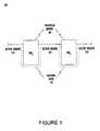
- FIG. 1illustrates an exemplary Shallow Trench Isolation scheme in accordance with one embodiment of the present invention.
- FIG. 2is the cross-sectional view of a single trench in accordance with one embodiment of the present invention.
- FIG. 3illustrates a cross-sectional view showing the grown Liner Oxide (LINOX) applied to the walls of the trench, in accordance with one embodiment of the present invention.
- LINOXLiner Oxide
- FIG. 4illustrates a cross-sectional view showing silicon dioxide trench filler deposited by Chemical Vapor Deposition (CVD) in accordance with one embodiment of the present invention.
- CVDChemical Vapor Deposition
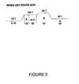
- FIG. 5is a process diagram of the recipe for annealing the LINOX in accordance with one embodiment of the present invention.
- FIG. 6is a cross-sectional view showing a poly line passing over a Shallow Trench Isolation (STI) region in accordance with one embodiment of the present invention.
- STIShallow Trench Isolation
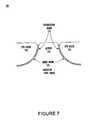
- FIG. 7illustrates a cross-sectional view showing possible damage after Poly/spacer etch in accordance with one embodiment of the present invention.
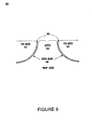
- FIG. 8illustrates a planar-view showing Poly/spacer edge overlapping an active area corner in accordance with one embodiment of the present invention.
- FIG. 9illustrates a cross-sectional view showing the minimal Poly/spacer etch damage after annealing the LINOX in accordance with one embodiment of the present invention.
- FIG. 1illustrates an exemplary Shallow Trench Isolation (STI) scheme in accordance with one embodiment of the present invention.
- An integrated circuitmay be realized by locating active semiconductor devices in the active regions 110 , 120 and 130 .
- Electrical isolation of active regionsmay be realized by the formation of shallow trenches in the surface of the semiconductor substrate between the active regions, which may then be filled with silicon dioxide to form isolation regions 140 .
- the minimization or elimination of electrical leakage currents between active regions along a leakage path 150is a primary objective.
- the process used to form isolation regions 140results in a reduction in electrical leakage currents between active regions when compared with prior art methods.
- FIG. 2is the cross-sectional view of a shallow trench 210 separating two active regions 220 and 230 in a semiconductor substrate 200 in accordance with one embodiment of the present invention.
- the trenchmay be formed by plasma etching.
- a small trench width 250may be preferred to accommodate smaller integrated circuit geometry.
- a larger trench depth 260may reduce electrical current leakage between active regions 220 and 230 .
- the plasma etch used to form the trenchresults in uneven trench surfaces 240 . These uneven surfaces lead to the formation of stress regions and dislocations in the active regions during subsequent processing steps as described below. Regions of stress and dislocations may in turn result in increased electrical leakage between active areas as well as active device failure.
- the shallow trenchhaving a width of at most 0.3 ⁇ with fallback widths of 0.25 ⁇ and 0.21 ⁇ .
- FIG. 3illustrates a cross-sectional view 300 showing the grown Liner Oxide (LINOX) 330 covering the uneven inner surfaces of the trench 340 .
- the trenchseparates the two active regions 310 and 320 . Since the LINOX 330 is grown, it becomes an integral part of the semiconductor substrate, as opposed to silicon dioxide that is deposited on the surface of the substrate by Chemical Vapor Deposition (CVD). Following the LINOX growth step, the temperature is elevated slightly for a period of time to anneal the LINOX 330 .
- the LINOX 330may be grown at a temperature of 1000 degrees centigrade, and annealing of the LINOX 330 may be accomplished over a period of 3 hours at a temperature of 1050 degrees centigrade.
- Annealingcauses an increase in density of the LINOX 330 which increases its strength and relieves stresses which may form along the trench surfaces at corners or at sharp edges.
- the increased strength of the LINOX 330causes it to be insensitive to subsequent processing steps. Relieving the stresses in the LINOX 330 (especially at the corners) may result in a reduction in or elimination of dislocations in the semiconductor substrate which in turn may reduce electrical leakage currents between active areas.
- An additional advantage of the present inventionis the accomplishment of denuding and gettering that occur during the annealing process.
- FIG. 4illustrates a cross-sectional view 400 of a Shallow Trench Isolation (STI) region 450 separating two active regions 410 and 420 .
- the silicon dioxide trench filler 430may be deposited by Chemical Vapor Deposition (CVD) in accordance with one embodiment of the present invention.
- the LINOX 440separates the deposited CVD oxide 430 from the semiconductor substrate active regions 410 and 420 .
- the large stresses that occur when oxide is deposited by CVD directly into a trench without the LINOXmay be eliminated.
- the dislocations formed in the semiconductor substrate due to these stressesmay also be eliminated in accordance with the present invention.
- FIG. 5is an exemplary process diagram 500 which may be used to grow a liner oxide (LINOX) in a shallow trench on a semiconductor substrate in accordance with one embodiment of the present invention.
- the semiconductor temperatureis stabilized in the presence of Argon at 1000 degrees centigrade.
- the LINOXis grown to the desired depth by holding the semiconductor at a temperature of 1000 degrees centigrade in the presence of oxygen and chlorine for a period of time.
- the semiconductor temperatureis then increased in step 530 to 1050 degrees centigrade for a period of three hours to accomplish the annealing of the LINOX.
- step 530the density of the LINOX is increased density, stresses between the LINOX and the semiconductor substrate are relieved, and denuding and gettering are both accomplished.
- step 540the temperature is then reduced to the starting point of 800 degrees centigrade for further processing. It is appreciated that other possible gases besides Argon can be used, and also other possible sources of oxygen can be used.
- polysilicon stripsas conductors.
- the poly 610may pass over both active regions 650 as well as isolation regions 620 and 630 .
- Etching of the poly, during a step referred to as poly/spacer etch,may gouge the liner oxide 640 at points of excessive stress 660 .
- FIG. 7is a cross-sectional view 700 illustrating regions where dislocations 710 may occur when the liner oxide 750 is not annealed.
- the combination of stress and gouging in the liner oxide 750may cause dislocations 710 in the active regions 740 of the semiconductor substrate as illustrated in FIG. 7 .
- Such dislocationsmay increase electrical current leakage around isolation regions 720 and 730 , and may result in active device failures.
- Such gouging and dislocation formationare particularly troublesome when a poly/spacer edge overlaps an active area at a sharp corner.
- FIG. 8illustrates a planar-view 800 of a semiconductor wafer.
- Two active regions 810are separated by a shallow trench isolation region 820 .
- An etched poly line 830overlaps a sharp corner of the upper active region 810 .
- the gouge region 840is an area where possible gouging and dislocations may occur as a result of the poly/spacer etch.
- annealing of the LINOX in the trench 820reduces or eliminates gouging during poly/spacer etch. As a result, dislocations are eliminated which reduces electrical current leakage between active regions.
- limitations on the layout of poly linesare relaxed since annealing the LINOX has eliminated the gouging problem.
- FIG. 9is the cross-sectional view 900 of an active area 930 separated by two isolation regions 910 and 920 in which the LINOX 940 has been annealed in accordance with one embodiment of the present invention.
- Annealing of the LINOXhas increased the density of the LINOX, reduced the stresses between the LINOX and the semiconductor active area.
- the gouging and resultant dislocations that may occur at points 950 during poly/spacer etchhave been eliminated.
- the problems caused by poly/spacer etch over active areas with sharp cornersno longer exist.
- prior limitations placed on the topology of poly lineshave been eliminated.
Landscapes
- Engineering & Computer Science (AREA)
- Physics & Mathematics (AREA)
- Condensed Matter Physics & Semiconductors (AREA)
- General Physics & Mathematics (AREA)
- Manufacturing & Machinery (AREA)
- Computer Hardware Design (AREA)
- Microelectronics & Electronic Packaging (AREA)
- Power Engineering (AREA)
- Chemical & Material Sciences (AREA)
- Chemical Kinetics & Catalysis (AREA)
- Element Separation (AREA)
- Semiconductor Memories (AREA)
Abstract
Description
Claims (11)
Priority Applications (1)
| Application Number | Priority Date | Filing Date | Title |
|---|---|---|---|
| US09/635,507US6817903B1 (en) | 2000-08-09 | 2000-08-09 | Process for reducing leakage in an integrated circuit with shallow trench isolated active areas |
Applications Claiming Priority (1)
| Application Number | Priority Date | Filing Date | Title |
|---|---|---|---|
| US09/635,507US6817903B1 (en) | 2000-08-09 | 2000-08-09 | Process for reducing leakage in an integrated circuit with shallow trench isolated active areas |
Publications (1)
| Publication Number | Publication Date |
|---|---|
| US6817903B1true US6817903B1 (en) | 2004-11-16 |
Family
ID=33418789
Family Applications (1)
| Application Number | Title | Priority Date | Filing Date |
|---|---|---|---|
| US09/635,507Expired - LifetimeUS6817903B1 (en) | 2000-08-09 | 2000-08-09 | Process for reducing leakage in an integrated circuit with shallow trench isolated active areas |
Country Status (1)
| Country | Link |
|---|---|
| US (1) | US6817903B1 (en) |
Cited By (5)
| Publication number | Priority date | Publication date | Assignee | Title |
|---|---|---|---|---|
| US20070066026A1 (en)* | 2005-09-16 | 2007-03-22 | Chih-Jen Mao | Method of preventing a peeling issue of a high stressed thin film |
| US20080054409A1 (en)* | 2006-08-31 | 2008-03-06 | Cheon-Man Shim | Fabricating method of semiconductor device |
| CN102122629A (en)* | 2010-01-08 | 2011-07-13 | 中芯国际集成电路制造(上海)有限公司 | Method for manufacturing lining oxide layer of shallow trench isolation (STI) |
| CN103681449A (en)* | 2012-09-13 | 2014-03-26 | 中芯国际集成电路制造(上海)有限公司 | Method for forming shallow trench isolation region |
| CN109004063A (en)* | 2018-07-06 | 2018-12-14 | 横店集团东磁股份有限公司 | A kind of thermal oxidation process of crystal silicon solar battery |
Citations (25)
| Publication number | Priority date | Publication date | Assignee | Title |
|---|---|---|---|---|
| US5427055A (en)* | 1992-01-31 | 1995-06-27 | Canon Kabushiki Kaisha | Method for controlling roughness on surface of monocrystal |
| US5447884A (en)* | 1994-06-29 | 1995-09-05 | International Business Machines Corporation | Shallow trench isolation with thin nitride liner |
| US5468676A (en) | 1992-09-23 | 1995-11-21 | Texas Instruments Incorporated | Trench isolation structure and method for forming |
| US5858858A (en) | 1996-05-21 | 1999-01-12 | Samsung Electronics Co., Ltd. | Annealing methods for forming isolation trenches |
| US5910018A (en) | 1997-02-24 | 1999-06-08 | Winbond Electronics Corporation | Trench edge rounding method and structure for trench isolation |
| US5950096A (en) | 1997-09-22 | 1999-09-07 | Lucent Technologies Inc. | Process for improving device yield in integrated circuit fabrication |
| US5960299A (en) | 1998-10-28 | 1999-09-28 | United Microelectronics Corp. | Method of fabricating a shallow-trench isolation structure in integrated circuit |
| US5994178A (en) | 1997-12-31 | 1999-11-30 | Texas Instruments - Acer Incorporated | Method of fabricating CMOS transistors with a planar shallow trench isolation |
| US6001706A (en) | 1997-12-08 | 1999-12-14 | Chartered Semiconductor Manufacturing, Ltd. | Method for making improved shallow trench isolation for semiconductor integrated circuits |
| US6005279A (en) | 1997-12-18 | 1999-12-21 | Advanced Micro Devices, Inc. | Trench edge spacer formation |
| US6004864A (en) | 1998-02-25 | 1999-12-21 | Taiwan Semiconductor Manufacturing Company Ltd. | Ion implant method for forming trench isolation for integrated circuit devices |
| US6013561A (en) | 1996-12-20 | 2000-01-11 | Hyundai Electronics Industries Co., Ltd. | Method for forming field oxide film of semiconductor device |
| US6020251A (en) | 1998-01-23 | 2000-02-01 | United Silicon Incorporated | Method of forming buried diffusion junctions in conjunction with shallow-trench isolation structures in a semiconductor device |
| US6033968A (en) | 1999-03-29 | 2000-03-07 | United Integrated Circuits Corp. | Method for forming a shallow trench isolation structure |
| US6037018A (en) | 1998-07-01 | 2000-03-14 | Taiwan Semiconductor Maufacturing Company | Shallow trench isolation filled by high density plasma chemical vapor deposition |
| US6037238A (en)* | 1999-01-04 | 2000-03-14 | Vanguard International Semiconductor Corporation | Process to reduce defect formation occurring during shallow trench isolation formation |
| US6140208A (en)* | 1999-02-05 | 2000-10-31 | International Business Machines Corporation | Shallow trench isolation (STI) with bilayer of oxide-nitride for VLSI applications |
| US6150234A (en)* | 1999-12-16 | 2000-11-21 | Vlsi Technology, Inc. | Trench-diffusion corner rounding in a shallow-trench (STI) process |
| US6277706B1 (en)* | 1997-06-13 | 2001-08-21 | Nec Corporation | Method of manufacturing isolation trenches using silicon nitride liner |
| US20010021595A1 (en)* | 1998-10-30 | 2001-09-13 | Taiwan Semiconductor Manufacturing Company | Sub-atmospheric pressure thermal chemical vapor deposition (SACVD) trench isolation method with attenuated surface sensitivity |
| US20010021567A1 (en)* | 2000-03-10 | 2001-09-13 | Nec Corporation. | Method of forming device isolation structure |
| US6319794B1 (en)* | 1998-10-14 | 2001-11-20 | International Business Machines Corporation | Structure and method for producing low leakage isolation devices |
| US20010044193A1 (en)* | 1998-08-17 | 2001-11-22 | Micron Technology, Inc. | Isolation structure and process therefor |
| US6350662B1 (en)* | 1999-07-19 | 2002-02-26 | Taiwan Semiconductor Manufacturing Company | Method to reduce defects in shallow trench isolations by post liner anneal |
| US6374770B1 (en)* | 1995-10-26 | 2002-04-23 | Applied Materials, Inc. | Apparatus for improving film stability of halogen-doped silicon oxide films |
- 2000
- 2000-08-09USUS09/635,507patent/US6817903B1/ennot_activeExpired - Lifetime
Patent Citations (25)
| Publication number | Priority date | Publication date | Assignee | Title |
|---|---|---|---|---|
| US5427055A (en)* | 1992-01-31 | 1995-06-27 | Canon Kabushiki Kaisha | Method for controlling roughness on surface of monocrystal |
| US5468676A (en) | 1992-09-23 | 1995-11-21 | Texas Instruments Incorporated | Trench isolation structure and method for forming |
| US5447884A (en)* | 1994-06-29 | 1995-09-05 | International Business Machines Corporation | Shallow trench isolation with thin nitride liner |
| US6374770B1 (en)* | 1995-10-26 | 2002-04-23 | Applied Materials, Inc. | Apparatus for improving film stability of halogen-doped silicon oxide films |
| US5858858A (en) | 1996-05-21 | 1999-01-12 | Samsung Electronics Co., Ltd. | Annealing methods for forming isolation trenches |
| US6013561A (en) | 1996-12-20 | 2000-01-11 | Hyundai Electronics Industries Co., Ltd. | Method for forming field oxide film of semiconductor device |
| US5910018A (en) | 1997-02-24 | 1999-06-08 | Winbond Electronics Corporation | Trench edge rounding method and structure for trench isolation |
| US6277706B1 (en)* | 1997-06-13 | 2001-08-21 | Nec Corporation | Method of manufacturing isolation trenches using silicon nitride liner |
| US5950096A (en) | 1997-09-22 | 1999-09-07 | Lucent Technologies Inc. | Process for improving device yield in integrated circuit fabrication |
| US6001706A (en) | 1997-12-08 | 1999-12-14 | Chartered Semiconductor Manufacturing, Ltd. | Method for making improved shallow trench isolation for semiconductor integrated circuits |
| US6005279A (en) | 1997-12-18 | 1999-12-21 | Advanced Micro Devices, Inc. | Trench edge spacer formation |
| US5994178A (en) | 1997-12-31 | 1999-11-30 | Texas Instruments - Acer Incorporated | Method of fabricating CMOS transistors with a planar shallow trench isolation |
| US6020251A (en) | 1998-01-23 | 2000-02-01 | United Silicon Incorporated | Method of forming buried diffusion junctions in conjunction with shallow-trench isolation structures in a semiconductor device |
| US6004864A (en) | 1998-02-25 | 1999-12-21 | Taiwan Semiconductor Manufacturing Company Ltd. | Ion implant method for forming trench isolation for integrated circuit devices |
| US6037018A (en) | 1998-07-01 | 2000-03-14 | Taiwan Semiconductor Maufacturing Company | Shallow trench isolation filled by high density plasma chemical vapor deposition |
| US20010044193A1 (en)* | 1998-08-17 | 2001-11-22 | Micron Technology, Inc. | Isolation structure and process therefor |
| US6319794B1 (en)* | 1998-10-14 | 2001-11-20 | International Business Machines Corporation | Structure and method for producing low leakage isolation devices |
| US5960299A (en) | 1998-10-28 | 1999-09-28 | United Microelectronics Corp. | Method of fabricating a shallow-trench isolation structure in integrated circuit |
| US20010021595A1 (en)* | 1998-10-30 | 2001-09-13 | Taiwan Semiconductor Manufacturing Company | Sub-atmospheric pressure thermal chemical vapor deposition (SACVD) trench isolation method with attenuated surface sensitivity |
| US6037238A (en)* | 1999-01-04 | 2000-03-14 | Vanguard International Semiconductor Corporation | Process to reduce defect formation occurring during shallow trench isolation formation |
| US6140208A (en)* | 1999-02-05 | 2000-10-31 | International Business Machines Corporation | Shallow trench isolation (STI) with bilayer of oxide-nitride for VLSI applications |
| US6033968A (en) | 1999-03-29 | 2000-03-07 | United Integrated Circuits Corp. | Method for forming a shallow trench isolation structure |
| US6350662B1 (en)* | 1999-07-19 | 2002-02-26 | Taiwan Semiconductor Manufacturing Company | Method to reduce defects in shallow trench isolations by post liner anneal |
| US6150234A (en)* | 1999-12-16 | 2000-11-21 | Vlsi Technology, Inc. | Trench-diffusion corner rounding in a shallow-trench (STI) process |
| US20010021567A1 (en)* | 2000-03-10 | 2001-09-13 | Nec Corporation. | Method of forming device isolation structure |
Non-Patent Citations (2)
| Title |
|---|
| Wolf et al., Siclicon Processing for the VLSI Era, Process Technology, Lattice Press, Sunset Beach, CA, USA, pp. 56-70, 1986.* |
| Wolf et al., Silicon Processing for the VLSI Era, vol. 1: Process Technology, Lattice Press, Sunset Beach, CA, USA, pp. 218-219, 228, 1986.** |
Cited By (7)
| Publication number | Priority date | Publication date | Assignee | Title |
|---|---|---|---|---|
| US20070066026A1 (en)* | 2005-09-16 | 2007-03-22 | Chih-Jen Mao | Method of preventing a peeling issue of a high stressed thin film |
| US7482244B2 (en)* | 2005-09-16 | 2009-01-27 | United Microelectronics Corp. | Method of preventing a peeling issue of a high stressed thin film |
| US20080054409A1 (en)* | 2006-08-31 | 2008-03-06 | Cheon-Man Shim | Fabricating method of semiconductor device |
| CN102122629A (en)* | 2010-01-08 | 2011-07-13 | 中芯国际集成电路制造(上海)有限公司 | Method for manufacturing lining oxide layer of shallow trench isolation (STI) |
| CN102122629B (en)* | 2010-01-08 | 2013-06-19 | 中芯国际集成电路制造(上海)有限公司 | Method for manufacturing lining oxide layer of shallow trench isolation (STI) |
| CN103681449A (en)* | 2012-09-13 | 2014-03-26 | 中芯国际集成电路制造(上海)有限公司 | Method for forming shallow trench isolation region |
| CN109004063A (en)* | 2018-07-06 | 2018-12-14 | 横店集团东磁股份有限公司 | A kind of thermal oxidation process of crystal silicon solar battery |
Similar Documents
| Publication | Publication Date | Title |
|---|---|---|
| US6875649B2 (en) | Methods for manufacturing integrated circuit devices including an isolation region defining an active region area | |
| US6881646B2 (en) | Semiconductor device and process for producing the same | |
| US6627512B2 (en) | Method of manufacturing a semiconductor device | |
| US5719085A (en) | Shallow trench isolation technique | |
| US5334556A (en) | Method for improving gate oxide integrity using low temperature oxidation during source/drain anneal | |
| US6350662B1 (en) | Method to reduce defects in shallow trench isolations by post liner anneal | |
| US4580330A (en) | Integrated circuit isolation | |
| US4561172A (en) | Integrated circuit fabrication method utilizing selective etching and oxidation to form isolation regions | |
| EP0428283A2 (en) | Method for local oxidation of silicon | |
| US20020037627A1 (en) | Extension of shallow trench isolation by ion implantation | |
| US10438837B2 (en) | Anneal after trench sidewall implant to reduce defects | |
| US7514337B2 (en) | Semiconductor device using EPI-layer and method of forming the same | |
| JPH05102296A (en) | Manufacture of shallow trench separation flattened in integrated circuit and constitution body that is fabricated therewith | |
| US6953734B2 (en) | Method for manufacturing shallow trench isolation in semiconductor device | |
| US4538343A (en) | Channel stop isolation technology utilizing two-step etching and selective oxidation with sidewall masking | |
| US6784042B2 (en) | Integration process on a SOI substrate of a semiconductor device comprising at least a dielectrically isolated well | |
| US6602792B2 (en) | Method for reducing stress of sidewall oxide layer of shallow trench isolation | |
| JP2682529B2 (en) | Method for forming element isolation insulating film of semiconductor element | |
| US6534379B1 (en) | Linerless shallow trench isolation method | |
| US6483148B2 (en) | Self-aligned elevated transistor | |
| US6817903B1 (en) | Process for reducing leakage in an integrated circuit with shallow trench isolated active areas | |
| US6258697B1 (en) | Method of etching contacts with reduced oxide stress | |
| US6333218B1 (en) | Method of etching contacts with reduced oxide stress | |
| US20040038495A1 (en) | Method of providing a thick thermal oxide in trench isolation | |
| US6309942B1 (en) | STI punch-through defects and stress reduction by high temperature oxide reflow process |
Legal Events
| Date | Code | Title | Description |
|---|---|---|---|
| AS | Assignment | Owner name:CYPRESS SEMICONDUCTOR CORPORATION, CALIFORNIA Free format text:ASSIGNMENT OF ASSIGNORS INTEREST;ASSIGNORS:RAMKUMAR, KRISHNASWAMY;WONG, KAICHIU;JAYATILAKA, VENUKA;REEL/FRAME:011032/0672;SIGNING DATES FROM 20000802 TO 20000806 | |
| STCF | Information on status: patent grant | Free format text:PATENTED CASE | |
| FPAY | Fee payment | Year of fee payment:4 | |
| FEPP | Fee payment procedure | Free format text:PAYOR NUMBER ASSIGNED (ORIGINAL EVENT CODE: ASPN); ENTITY STATUS OF PATENT OWNER: LARGE ENTITY Free format text:PAYER NUMBER DE-ASSIGNED (ORIGINAL EVENT CODE: RMPN); ENTITY STATUS OF PATENT OWNER: LARGE ENTITY | |
| FPAY | Fee payment | Year of fee payment:8 | |
| AS | Assignment | Owner name:MORGAN STANLEY SENIOR FUNDING, INC., NEW YORK Free format text:SECURITY INTEREST;ASSIGNORS:CYPRESS SEMICONDUCTOR CORPORATION;SPANSION LLC;REEL/FRAME:035240/0429 Effective date:20150312 | |
| FPAY | Fee payment | Year of fee payment:12 | |
| SULP | Surcharge for late payment | Year of fee payment:11 | |
| AS | Assignment | Owner name:SPANSION LLC, CALIFORNIA Free format text:PARTIAL RELEASE OF SECURITY INTEREST IN PATENTS;ASSIGNOR:MORGAN STANLEY SENIOR FUNDING, INC., AS COLLATERAL AGENT;REEL/FRAME:039708/0001 Effective date:20160811 Owner name:CYPRESS SEMICONDUCTOR CORPORATION, CALIFORNIA Free format text:PARTIAL RELEASE OF SECURITY INTEREST IN PATENTS;ASSIGNOR:MORGAN STANLEY SENIOR FUNDING, INC., AS COLLATERAL AGENT;REEL/FRAME:039708/0001 Effective date:20160811 | |
| AS | Assignment | Owner name:MONTEREY RESEARCH, LLC, CALIFORNIA Free format text:ASSIGNMENT OF ASSIGNORS INTEREST;ASSIGNOR:CYPRESS SEMICONDUCTOR CORPORATION;REEL/FRAME:040911/0238 Effective date:20160811 | |
| AS | Assignment | Owner name:MORGAN STANLEY SENIOR FUNDING, INC., NEW YORK Free format text:CORRECTIVE ASSIGNMENT TO CORRECT THE 8647899 PREVIOUSLY RECORDED ON REEL 035240 FRAME 0429. ASSIGNOR(S) HEREBY CONFIRMS THE SECURITY INTERST;ASSIGNORS:CYPRESS SEMICONDUCTOR CORPORATION;SPANSION LLC;REEL/FRAME:058002/0470 Effective date:20150312 |