US6816147B2 - Bistable electro-optic display, and method for addressing same - Google Patents
Bistable electro-optic display, and method for addressing sameDownload PDFInfo
- Publication number
- US6816147B2 US6816147B2US09/931,418US93141801AUS6816147B2US 6816147 B2US6816147 B2US 6816147B2US 93141801 AUS93141801 AUS 93141801AUS 6816147 B2US6816147 B2US 6816147B2
- Authority
- US
- United States
- Prior art keywords
- electro
- deformable member
- optic
- movable member
- optic material
- Prior art date
- Legal status (The legal status is an assumption and is not a legal conclusion. Google has not performed a legal analysis and makes no representation as to the accuracy of the status listed.)
- Expired - Fee Related, expires
Links
- 238000000034methodMethods0.000titleclaimsdescription23
- 239000000382optic materialSubstances0.000claimsabstractdescription89
- 239000002245particleSubstances0.000claimsdescription36
- 239000000463materialSubstances0.000claimsdescription29
- 239000012530fluidSubstances0.000claimsdescription16
- 239000002775capsuleSubstances0.000claimsdescription14
- 230000005684electric fieldEffects0.000claimsdescription12
- 239000007788liquidSubstances0.000claimsdescription9
- 238000007789sealingMethods0.000claimsdescription9
- 238000007639printingMethods0.000claimsdescription6
- 230000003287optical effectEffects0.000claimsdescription5
- 230000037230mobilityEffects0.000claimsdescription2
- 230000002093peripheral effectEffects0.000claimsdescription2
- 239000003094microcapsuleSubstances0.000description9
- 238000000576coating methodMethods0.000description6
- 239000011248coating agentSubstances0.000description5
- 239000011159matrix materialSubstances0.000description5
- 101100351283Homo sapiens PDE6D geneProteins0.000description4
- 102100037593Retinal rod rhodopsin-sensitive cGMP 3',5'-cyclic phosphodiesterase subunit deltaHuman genes0.000description4
- 239000012769display materialSubstances0.000description4
- 239000000049pigmentSubstances0.000description3
- 229920000642polymerPolymers0.000description3
- GWEVSGVZZGPLCZ-UHFFFAOYSA-NTitan oxideChemical compoundO=[Ti]=OGWEVSGVZZGPLCZ-UHFFFAOYSA-N0.000description2
- 239000011230binding agentSubstances0.000description2
- 239000004020conductorSubstances0.000description2
- 230000000694effectsEffects0.000description2
- 239000004973liquid crystal related substanceSubstances0.000description2
- 239000004215Carbon black (E152)Substances0.000description1
- 230000002411adverseEffects0.000description1
- 238000007754air knife coatingMethods0.000description1
- 230000002457bidirectional effectEffects0.000description1
- 239000001045blue dyeSubstances0.000description1
- 239000002131composite materialSubstances0.000description1
- 238000007766curtain coatingMethods0.000description1
- 238000007607die coating methodMethods0.000description1
- 238000003618dip coatingMethods0.000description1
- 239000000428dustSubstances0.000description1
- 229920001971elastomerPolymers0.000description1
- 238000007765extrusion coatingMethods0.000description1
- 229920005570flexible polymerPolymers0.000description1
- 239000006260foamSubstances0.000description1
- 238000007756gravure coatingMethods0.000description1
- 229930195733hydrocarbonNatural products0.000description1
- 150000002430hydrocarbonsChemical class0.000description1
- AMGQUBHHOARCQH-UHFFFAOYSA-Nindium;oxotinChemical compound[In].[Sn]=OAMGQUBHHOARCQH-UHFFFAOYSA-N0.000description1
- 238000007641inkjet printingMethods0.000description1
- 238000009685knife-over-roll coatingMethods0.000description1
- 230000007774longtermEffects0.000description1
- 239000000314lubricantSubstances0.000description1
- 238000004519manufacturing processMethods0.000description1
- 239000012528membraneSubstances0.000description1
- 230000005499meniscusEffects0.000description1
- 238000012986modificationMethods0.000description1
- 230000004048modificationEffects0.000description1
- 229920003052natural elastomerPolymers0.000description1
- 229920001194natural rubberPolymers0.000description1
- 238000009877renderingMethods0.000description1
- 238000012827research and developmentMethods0.000description1
- 238000007763reverse roll coatingMethods0.000description1
- 239000005060rubberSubstances0.000description1
- 238000007650screen-printingMethods0.000description1
- 239000007787solidSubstances0.000description1
- 238000004528spin coatingMethods0.000description1
- 238000005507sprayingMethods0.000description1
- 239000000758substrateSubstances0.000description1
- 230000002459sustained effectEffects0.000description1
- 229920003051synthetic elastomerPolymers0.000description1
- 239000005061synthetic rubberSubstances0.000description1
- 238000007651thermal printingMethods0.000description1
Images

Classifications
- G—PHYSICS
- G02—OPTICS
- G02F—OPTICAL DEVICES OR ARRANGEMENTS FOR THE CONTROL OF LIGHT BY MODIFICATION OF THE OPTICAL PROPERTIES OF THE MEDIA OF THE ELEMENTS INVOLVED THEREIN; NON-LINEAR OPTICS; FREQUENCY-CHANGING OF LIGHT; OPTICAL LOGIC ELEMENTS; OPTICAL ANALOGUE/DIGITAL CONVERTERS
- G02F1/00—Devices or arrangements for the control of the intensity, colour, phase, polarisation or direction of light arriving from an independent light source, e.g. switching, gating or modulating; Non-linear optics
- G02F1/01—Devices or arrangements for the control of the intensity, colour, phase, polarisation or direction of light arriving from an independent light source, e.g. switching, gating or modulating; Non-linear optics for the control of the intensity, phase, polarisation or colour
- G02F1/165—Devices or arrangements for the control of the intensity, colour, phase, polarisation or direction of light arriving from an independent light source, e.g. switching, gating or modulating; Non-linear optics for the control of the intensity, phase, polarisation or colour based on translational movement of particles in a fluid under the influence of an applied field
- G02F1/166—Devices or arrangements for the control of the intensity, colour, phase, polarisation or direction of light arriving from an independent light source, e.g. switching, gating or modulating; Non-linear optics for the control of the intensity, phase, polarisation or colour based on translational movement of particles in a fluid under the influence of an applied field characterised by the electro-optical or magneto-optical effect
- G02F1/167—Devices or arrangements for the control of the intensity, colour, phase, polarisation or direction of light arriving from an independent light source, e.g. switching, gating or modulating; Non-linear optics for the control of the intensity, phase, polarisation or colour based on translational movement of particles in a fluid under the influence of an applied field characterised by the electro-optical or magneto-optical effect by electrophoresis
- G—PHYSICS
- G02—OPTICS
- G02F—OPTICAL DEVICES OR ARRANGEMENTS FOR THE CONTROL OF LIGHT BY MODIFICATION OF THE OPTICAL PROPERTIES OF THE MEDIA OF THE ELEMENTS INVOLVED THEREIN; NON-LINEAR OPTICS; FREQUENCY-CHANGING OF LIGHT; OPTICAL LOGIC ELEMENTS; OPTICAL ANALOGUE/DIGITAL CONVERTERS
- G02F1/00—Devices or arrangements for the control of the intensity, colour, phase, polarisation or direction of light arriving from an independent light source, e.g. switching, gating or modulating; Non-linear optics
- G02F1/01—Devices or arrangements for the control of the intensity, colour, phase, polarisation or direction of light arriving from an independent light source, e.g. switching, gating or modulating; Non-linear optics for the control of the intensity, phase, polarisation or colour
- G02F1/165—Devices or arrangements for the control of the intensity, colour, phase, polarisation or direction of light arriving from an independent light source, e.g. switching, gating or modulating; Non-linear optics for the control of the intensity, phase, polarisation or colour based on translational movement of particles in a fluid under the influence of an applied field
- G02F1/1675—Constructional details
- G02F1/16756—Insulating layers
Definitions
- This inventionrelates to a a bistable electro-optic material display and to a method for addressing such a display.
- electro-optic materialis used herein in its conventional meaning in the art to refer to a material having first and second display states differing in at least one optical property, the material being capable of being changed from its first to its second display state by application of an electric field to the material.
- bistabilityare used herein in their conventional meanings in the art to refer to displays comprising display elements having first and second display states differing in at least one optical property, and such that after any given element has been driven, by means of an addressing pulse of finite duration, to assume either its first or second display state, after the addressing pulse has terminated, that state will persist for at least several times the minimum duration of the addressing pulse required to change the state of the display element.
- addressing pulseof finite duration
- Electrophoretic and other electro-optic displayshave been the subject of intense research and development for a number of years. Such displays can have attributes of good brightness and contrast, wide viewing angles, state bistability, and low power consumption when compared with liquid crystal displays. Nevertheless, problems with the long-term image quality of electrophoretic displays have prevented their widespread usage. For example, particles that make up electrophoretic displays tend to cluster and settle, resulting in inadequate service-life for these displays.
- An encapsulated, electrophoretic displaytypically does not suffer from the clustering and settling failure mode of traditional electrophoretic devices and provides further advantages, such as the ability to print or coat the display on a wide variety of flexible and rigid substrates.
- printingis intended to include all forms of printing and coating, including, but without limitation: pre-metered coatings such as patch die coating, slot or extrusion coating, slide or cascade coating, curtain coating; roll coating such as knife over roll coating, forward and reverse roll coating; gravure coating; dip coating; spray coating; meniscus coating; spin coating; brush coating; air knife coating; silk screen printing processes; electrostatic printing processes; thermal printing processes; ink jet printing processes; and other similar techniques.
- pre-metered coatingssuch as patch die coating, slot or extrusion coating, slide or cascade coating, curtain coating
- roll coatingsuch as knife over roll coating, forward and reverse roll coating
- gravure coatingdip coating
- spray coatingmeniscus coating
- spin coatingspin coating
- brush coatingair knife coating
- silk screen printing processeselectrostatic printing processes
- Such display materialsare addressed using (a) a “direct-drive” addressing scheme, in which each pixel is provided with a separate electrode which can be addressed via its own drive line; (b) an active matrix addressing scheme in which each pixel is provided with an associated non-linear element (such as a transistor); or (c) a moving head addressing scheme, in which a head containing a number of individually controllable discrete electrodes is moved across the display, so that each electrode writes one line of the display.
- a “direct-drive” addressing schemein which each pixel is provided with a separate electrode which can be addressed via its own drive line
- an active matrix addressing schemein which each pixel is provided with an associated non-linear element (such as a transistor)
- a moving head addressing schemein which a head containing a number of individually controllable discrete electrodes is moved across the display, so that each electrode writes one line of the display.
- a direct-drive addressing schemeis practicable for a textual display (see, for example, International Application PCT/US99/16652, Publication No. WO 00/05704, which describes such a display using 63 electrodes for each text character) but impracticable for a graphic display, since providing the large number of drive lines required for a graphic display would necessitate excessively complex and expensive circuitry.
- Active matrix addressing schemesrequire complex and relatively expensive circuitry, the cost of which typically far exceeds the cost of the electro-optic medium itself.
- the present inventionseeks to provide an electro-optic display, and a method for addressing such a display, which are comparable in cost and complexity to a moving head addressing scheme, but which reduce or eliminate frictional wear on the electro-optic material and which are less susceptible to unevenness of the electro-optic material.
- an electro-optic displaycomprising:
- bistable electro-optic materialhaving on one side thereof a viewing surface on which the display can be viewed, and on the opposed side thereof a writing surface;
- a deformable memberdisposed adjacent but spaced from the writing surface of the electro-optic material, the deformable member bearing a plurality of elongate electrodes formed on its surface facing the writing surface of the electro-optic material;
- a movable memberdisposed on the opposed side of the deformable member from the electro-optic material and movable relative to the deformable member in a direction substantially parallel to the length of the elongate electrodes, the movable member contacting and deforming the deformable member such that a portion of each elongate electrode contacts or lies closely adjacent the writing surface of the electro-optic material.
- This inventionalso provides a method for addressing an electro-optic display of the invention as defined above.
- the movable memberis placed in a first position relative to the deformable member and a first set of potentials are placed on the elongate electrodes, thereby writing a first column of pixels of the display, each of this column of pixels being defined by the portion of one elongate electrode which contacts or lies closely adjacent the writing surface of the electro-optic material when the movable member is in its first position.
- the movable memberis then moved to a second position relative to the deformable member, this second position being spaced from the first position, and a second set of potentials are placed on the elongate electrodes, at least one of the second set of potentials differing from the first set of potentials, thereby writing a second column of pixels of the display, each of this column of pixels being defined by the portion of one elongate electrode which contacts or lies closely adjacent the writing surface of the electro-optic material when the movable member is in its second position.
- FIG. 1is a cross section through a preferred display of the present invention, this section being taken in a vertical plane perpendicular to the viewing surface of the display;
- FIG. 2is a top plan view of the display shown in FIG. 1 with the electro-optic material, front electrode and window removed to show details of the deformable member.
- the movable membercreates a “transverse wave” which travels along the deformable member and, as any physicist knows, in such a wave particles moved by the wave (in this case, the sections of the deformable member) do not move in the direction of travel of the wave but only perpendicular thereto.
- the deformable membercan be made with considerable elasticity (the deformable member may have the form of a thin sheet of a flexible material, for example a “blanket” made from a rubber or a flexible polymer), the deformable member can conform to any slight unevenness of the electro-optic material, thus rendering the display less sensitive to such unevenness.
- the movable membercan also be made compliant to assist in the deformable member conforming to any unevenness in the surface of the electro-optic material.
- the portion of the movable member which contacts the deformable membermay itself be deformable; for example, a rotatable movable member (as to which, see further below) may comprise a substantially rigid core and a deformable sleeve (formed for instance from a semi-rigid foam polymer) surrounding the core and contacting the deformable member.
- a rotatable movable memberas to which, see further below
- a deformable sleeveformed for instance from a semi-rigid foam polymer
- the electro-optic material used in the present displaymay be any such material which is bistable for a period at least equal to the time needed to write the entire display.
- the electro-optic materialmay be an electrophoretic material comprising electrically charged particles suspended in a fluid and capable of moving therethrough when an electric field is applied to the material.
- an electrophoretic materialbe of the encapsulated type in which the charged particles and the fluid are contained with a plurality of capsules (sometimes called “microcapsules”).
- the capsulesmay be dispersed in a binder and may be of any size or shape.
- the capsulesmay be spherical or non-spherical and their diameters may range from a few microns to a few millimeters, but are preferably in the range of from about 10 to a few hundred microns.
- the capsulesmay contain two or more different types of charged particles, and these particles may be colored, luminescent, the light-absorbing or transparent, and may include neat pigments, dyed (laked) pigments or pigment/polymer composites.
- an encapsulated electrophoretic displayincludes one or more species of particles that either absorb or scatter light.
- a displaymay comprise a plurality of capsules each of which contains one or more species of charged particles in a dyed suspending fluid.
- the displaymight comprise a plurality of capsules each of which contains, in a substantially uncolored suspending fluid, at least two species of charged particles differing in at least one optical characteristic and having differing electrophoretic mobilities; typically, one species of particle absorbs light (and is thus black or dark), while the other species of particle scatters light (and is thus white or light).
- the displaymay contain more than two species of particles, the suspending fluid may be clear or dyed, etc.
- the electro-optic material used in the present displaymay also have the form of a “polymer-dispersed electrophoretic display”, hereafter abbreviated “PDED”.
- PDEDpolymer-dispersed electrophoretic display
- a PDEDis a two-phase system in which the electrophoretic material comprises a continuous phase and a discontinuous phase.
- the discontinuous phasecomprises a plurality of droplets of an electrophoretic fluid (as usual, comprising a liquid and at least one particle disposed within the liquid and capable of moving therethrough on application of an electric field to the liquid), and the continuous phase (which is typically a polymeric material, although other materials may be useful) surrounds and encapsulates the discontinuous phases.
- the discrete droplets of electrophoretic fluid within a PDEDmay be referred to as capsules or microcapsules even though no discrete capsule membrane is associated with each individual droplet. Accordingly, references to “capsules” herein are to be construed as extending to PDED's, which are considered to be subsets of encapsulated electrophoretic displays.
- Electrophoretic displays of the present inventioncan make use of any known materials and processes for the production of such displays, as described, for example, in U.S. Pat. Nos. 5,930,026; 5,961,804; 6,017,584; 6,067,185; 6,118,426; 6,120,588; 6,120,839; 6,124,851; 6,130,773; 6,130,774; 6,172,798; 6,177,921; 6,232,950; 6,249,721; and 6,252,564, and International Applications Publication Nos.
- the electro-optic material used in the present displaycan also be of the rotating bichromal member type, as described, for example in U.S. Pat. No. 5,808,783 (Crowley), U.S. Pat. No. 5,777,782 (Sheridon) and U.S. Pat. No. 5,760,761 (Sheridon).
- this type of mediumis typically referred to as a “rotating bichromal ball” medium
- the term “rotating bichromal member”is believed more accurate, since the rotating members are not always spheres; for example, U.S. Pat. Nos. 5,894,367; 5,922,268; 6,055,091; and 6,097,531 describe electro-optic materials of this type in which the rotating members are cylindrical, while U.S.
- Pat. No. 6,147,791describes electro-optic materials in which the rotating members are polygonal prisms. It should also be understood that the term “bichromal” is used in a broad sense to mean “having at least two segments differing in an optical characteristic”; for example, U.S. Pat. Nos. 5,751,268; 5,891,479; 5,892,497; and 5,919,409 describe electro-optic materials of this type using rotating balls having more than two contrasting segments, and some of these segments may be transparent.
- bistable electro-optic materialsmay also be used on the apparatus and method of the present invention.
- the deformable member used in the present displaymay be formed from any flexible material having sufficient toughness to withstand repeated passages of the movable member thereacross.
- the deformable member wellcomprise a thin sheet or film of a natural or synthetic rubber or a polymer.
- the elongate electrodes on the deformable memberare conveniently formed by printing (as previously defined) a conductive ink on to the deformable member; since electrophoretic displays draw very little current, such displays can be used with electrodes having relatively high resistances.
- the portion of the deformable member which contacts the electro-optic materiallie flat against the electro-optic material without creasing or distortion, and to avoid such creasing or distortion the deformable member should be disposed spaced from, but parallel to, the electro-optic material.
- the manner in which the deformable member is maintained parallel to the electro-optic materialmay vary depending upon the orientation of these two members. For example, if the electro-optic material is in the form of a flat, horizontally-disposed sheet, a horizontal support surface could be provided parallel to the electro-optic material, and the deformable member allowed to rest upon this support surface, with the movable member passing over the support surface.
- the electro-optic materialis disposed in a substantially vertical plane, it may be convenient to keep the deformable member parallel to the electro-optic material by providing tensioning means for holding the deformable member under tension such that portions of the deformable member not in contact with the movable member will be held spaced from the electro-optic material.
- tensioning meansfor holding the deformable member under tension such that portions of the deformable member not in contact with the movable member will be held spaced from the electro-optic material.
- one pair of opposed edges of the electro-optic materialcould be provided with projecting ridges or flanges extending toward the deformable member, with the deformable member being stretched under tension across these ridges or flanges, and the movable member passing between the ridges or flanges to contact central portions of the deformable member with the electro-optic material.
- the movable member used in the display of the present inventionmay simply slide across the deformable member.
- it is desirable that such friction be reduced as far as possiblefor example by providing a smoothly rounded surface on the part of the movable member which contacts the deformable member and/or by providing a friction-reducing layer (formed, for example, from a solid lubricant) on one or both members.
- the movable memberbe rotatable so that the movable member can roll across the deformable member, desirably with minimal friction.
- the size of the pixels of the displayis controlled by the area of contact of each individual electrode on the deformable member with the electro-optic material, and to this area is in turn controlled by the area of contact between the movable member and the deformable member, it is desirable that the diameter of the movable member be reduced as far as possible, provided that this diameter is not reduced so far that the movement of the movable member will cause excessive wear on or damage to the deformable member. Because of this limitation on pixel size imposed by the area of contact between each electrode and the electro-optic material, the present display will typically not be used for high resolution displays.
- the present displayis well-suited for use in inexpensive, low resolution displays, for example in toys or low cost message pads or boards intended for domestic use, and is also well-suited for use in very large displays, for example billboard-type signs in sports arenas, or message boards in convention or exhibition halls, where large pixels are not objectionable but where the large area of the sign would render either direct drive or active matrix addressing schemes impracticably costly.
- the deformable memberlie flat against the electro-optic material to ensure that a consistent electric field is applied to this material.
- the movable memberbe provided with biasing means for urging the movable member into engagement with the deformable member, and hence urging the deformable member to contact the electro-optic material.
- sealing meansfor preventing entry of small particles between the electro-optic material and the deformable member, since even very small particles may be sufficient to affect the proper operation of the display.
- Such a sealing meanscould comprise a sealing member sealingly engaged with peripheral portions of both the electro-optic material and the deformable member so as to form a closed chamber between the writing surface of the electro-optic material and the electrode-carrying surface of the deformable member.
- the sealing meansmay comprise a sealed housing enclosing the electro-optic material, the deformable member and the movable member.
- Such a sealed housingwill of course also prevent entry of dust and other small particles between the deformable member and the movable member; this may be desirable, but is of less concern than entry of particles between the electro-optic material and the deformable member since the flexibility of the deformable member, and optionally that of the movable member will usually accommodate small particles therebetween without adverse effects on the performance of the display.
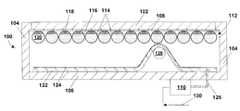
- the display(generally designated 100 ) shown in FIGS. 1 and 2 of the accompanying drawings comprises a cuboidal housing, which itself comprises a transparent window 102 (through which an observer views the display), sidewalls 104 and a rear wall 106 .
- a transparent electrode 108On the inner surface of the window 102 is provided a transparent electrode 108 , which may be formed from, for example, indium-tin oxide, and which extends across the whole area of the display 100 .
- This electrode 108is maintained at ground potential by means of a connection (not shown) to a control unit 110 mounted on the rear wall 106 of the housing.
- Electro-optic material 112On the inner surface of the electrode 108 is coated a layer (generally designated 112 ) of electro-optic material.
- the surface (the upper surface as illustrated in FIG. 1) of the electro-optic material 112 adjacent the electrode 108is visible to an observer viewing the display through the the transparent window 102 and the transparent electrode 108 and thus form a “viewable surface” of the electro-optic material 112 .
- This electro-optic materialis an encapsulated electrophoretic medium of the type described in, for example, U.S. Pat. No.
- the 6,067,185comprises a plurality of microcapsules 114 , each of which comprises a capsule wall 116 , which encloses an internal phase comprising a single type of charged particle 118 (assumed for present purposes to be negatively-charged, though obviously a positively-charged particle could equally well be used) dispersed in a colored liquid 120 .
- the charged particles 118comprise titania particles, negatively charged and having a diameter of about 250 nm, while the liquid 120 comprises a hydrocarbon having dissolved therein a blue dye.
- the size of the microcapsules 114is greatly exaggerated in FIG. 1 .
- microcapsules 114are shown as spherical in FIG. 1, in fact, for reasons explained in the aforementioned U.S. Pat. No. 6,067,185, it is preferred that the microcapsules have a flattened, non-spherical form.
- the display 100further comprises a deformable member 122 , which comprises a thin sheet of flexible material and which carries on its upper surface (the surface facing the electro-optic layer 112 ) a plurality of parallel elongate electrodes 124 (best seen in FIG. 2 ). Each of the electrodes 124 is connected via an associated conductor 126 (only one of these conductors is shown in FIG. 1 ), which extends through the deformable member 122 and the rear wall 106 , to the control unit 110 .
- the major portion of the deformable member 122rests upon the upper surface of the rear wall 106 ; thus, this upper surface serves as a support surface for the deformable member 122 .
- a cylindrical and rotatable movable member 128is positioned between the deformable member 122 and the upper surface of the rear wall 106 ; the movable member 128 is disposed so that the small portions of the electrodes 124 on the deformable member 122 lying directly on top of the movable member 128 contact the electro-optic layer 112 .
- these small portions of the electrodesdefine one column of pixels of the display 100 .
- the movable member 128is provided with drive means (not shown) which translate it in either direction parallel to the length of the electrodes 124 , i.e., left-right in FIG. 1 .
- the movable membercan be provided at each end with a threaded aperture engaged with a threaded drive rod, which is rotated by an electric motor under the control of the control unit 110 .
- the movement of the movable member 128causes different portions of the electrodes 124 on the deformable member 122 to contact the lower surface (as illustrated in FIG. 1) of the electro-optic layer 112 , thus enabling different portions of this layer to be rewritten.
- the lower surface of the electro-optic layer 112serves as a writing surface.
- the control unit 110is arranged to receive digital graphic image files in any convenient file format via an input line 130 and to generate signals of +V, 0 or ⁇ V on each of the electrodes 124 . Since the particles 118 within the microcapsules 114 are negatively charged, if a signal of ⁇ V is applied to an electrode 124 , the particles 118 in the microcapsules 114 adjacent the portion of that electrode 124 in contact with the electro-optic layer 112 will be repelled from the electrode 124 and will gather adjacent the electrode 108 . Thus, an observer viewing the display through the window 102 will see the color of the particles 118 , and the pixel will appear white.
- a signal of +Vis applied to the electrode 124 , the particles 118 in the microcapsules 114 adjacent the portion of that electrode 124 in contact with the electro-optic layer 112 will be attracted to, and gather adjacent, that electrode 124 .
- an observer viewing the display through the window 102will see the color of the colored liquid 120 , typically blue.
- a signal of 0is applied to an electrode 124 , the particles 118 adjacent the portion of that electrode 124 in contact with the electro-optic layer 112 will experience no electric field, and thus the pixel will remain in the same state as it was previously.
- the present inventionprovides an electro-optic display in which wear on the electro-optic material is substantially reduced, as compared with a similar conventional moving head display.
- the display of the present inventioncan also be made less susceptible to slight unevenness in the electro-optic material than conventional moving head displays.
Landscapes
- Physics & Mathematics (AREA)
- Nonlinear Science (AREA)
- General Physics & Mathematics (AREA)
- Optics & Photonics (AREA)
- Health & Medical Sciences (AREA)
- Life Sciences & Earth Sciences (AREA)
- Chemical & Material Sciences (AREA)
- Chemical Kinetics & Catalysis (AREA)
- Electrochemistry (AREA)
- Molecular Biology (AREA)
- Electrochromic Elements, Electrophoresis, Or Variable Reflection Or Absorption Elements (AREA)
Abstract
Description
This application claims priority from Provisional Application Ser. No. 60/226,064, filed Aug. 17, 2000, the entire disclosure of which is herein incorporated by reference.
This invention relates to a a bistable electro-optic material display and to a method for addressing such a display. The term “electro-optic material” is used herein in its conventional meaning in the art to refer to a material having first and second display states differing in at least one optical property, the material being capable of being changed from its first to its second display state by application of an electric field to the material. The terms “bistable” and “bistability” are used herein in their conventional meanings in the art to refer to displays comprising display elements having first and second display states differing in at least one optical property, and such that after any given element has been driven, by means of an addressing pulse of finite duration, to assume either its first or second display state, after the addressing pulse has terminated, that state will persist for at least several times the minimum duration of the addressing pulse required to change the state of the display element. These terms are also to be construed to include materials having more than two display states which are stable in this manner.
Electrophoretic and other electro-optic displays have been the subject of intense research and development for a number of years. Such displays can have attributes of good brightness and contrast, wide viewing angles, state bistability, and low power consumption when compared with liquid crystal displays. Nevertheless, problems with the long-term image quality of electrophoretic displays have prevented their widespread usage. For example, particles that make up electrophoretic displays tend to cluster and settle, resulting in inadequate service-life for these displays.
An encapsulated, electrophoretic display typically does not suffer from the clustering and settling failure mode of traditional electrophoretic devices and provides further advantages, such as the ability to print or coat the display on a wide variety of flexible and rigid substrates. (Use of the word “printing” is intended to include all forms of printing and coating, including, but without limitation: pre-metered coatings such as patch die coating, slot or extrusion coating, slide or cascade coating, curtain coating; roll coating such as knife over roll coating, forward and reverse roll coating; gravure coating; dip coating; spray coating; meniscus coating; spin coating; brush coating; air knife coating; silk screen printing processes; electrostatic printing processes; thermal printing processes; ink jet printing processes; and other similar techniques.) Thus, the resulting display can be flexible. Further, because the display medium can be printed (using a variety of methods), the display itself can be made inexpensively.
One problem in addressing electrophoretic and similar electro-optic display materials is that typically such materials do not exhibit any significant threshold, i.e., even a small electric field will cause the material to change its display state if the small field is sustained for a considerable period of time. Consequently, it is usually not possible to address such materials using a passive matrix addressing scheme such as is often used with liquid crystal displays. Accordingly, such display materials are addressed using (a) a “direct-drive” addressing scheme, in which each pixel is provided with a separate electrode which can be addressed via its own drive line; (b) an active matrix addressing scheme in which each pixel is provided with an associated non-linear element (such as a transistor); or (c) a moving head addressing scheme, in which a head containing a number of individually controllable discrete electrodes is moved across the display, so that each electrode writes one line of the display.
All three of these addressing schemes have disadvantages. A direct-drive addressing scheme is practicable for a textual display (see, for example, International Application PCT/US99/16652, Publication No. WO 00/05704, which describes such a display using 63 electrodes for each text character) but impracticable for a graphic display, since providing the large number of drive lines required for a graphic display would necessitate excessively complex and expensive circuitry. Active matrix addressing schemes require complex and relatively expensive circuitry, the cost of which typically far exceeds the cost of the electro-optic medium itself. Furthermore, since the cost of producing active matrix addressing circuitry is typically directly proportional to the area of the display, this type of addressing scheme is impracticable for very large displays, for example signs intended as electronic billboards in sports stadia or as message boards in large exhibition halls. Moving head addressing schemes tend to be inexpensive but, since the head needs to be in intimate contact with the electro-optic medium to produce the large electric fields needed to change the display state of most electro-optic materials, the friction between the moving head and the electro-optic material causes wear on the material and limits the life of the display. Furthermore, a moving head is highly sensitive to any slight unevenness in the display material, and in very large signs it is difficult to avoid such unevenness in the display material, especially if the large sign is to be used outdoors, where wind gusts might slightly distort the medium.
The present invention seeks to provide an electro-optic display, and a method for addressing such a display, which are comparable in cost and complexity to a moving head addressing scheme, but which reduce or eliminate frictional wear on the electro-optic material and which are less susceptible to unevenness of the electro-optic material.
Accordingly, this invention provides an electro-optic display comprising:
a bistable electro-optic material having on one side thereof a viewing surface on which the display can be viewed, and on the opposed side thereof a writing surface;
a deformable member disposed adjacent but spaced from the writing surface of the electro-optic material, the deformable member bearing a plurality of elongate electrodes formed on its surface facing the writing surface of the electro-optic material; and
a movable member disposed on the opposed side of the deformable member from the electro-optic material and movable relative to the deformable member in a direction substantially parallel to the length of the elongate electrodes, the movable member contacting and deforming the deformable member such that a portion of each elongate electrode contacts or lies closely adjacent the writing surface of the electro-optic material.
This invention also provides a method for addressing an electro-optic display of the invention as defined above. In this addressing method, the movable member is placed in a first position relative to the deformable member and a first set of potentials are placed on the elongate electrodes, thereby writing a first column of pixels of the display, each of this column of pixels being defined by the portion of one elongate electrode which contacts or lies closely adjacent the writing surface of the electro-optic material when the movable member is in its first position. The movable member is then moved to a second position relative to the deformable member, this second position being spaced from the first position, and a second set of potentials are placed on the elongate electrodes, at least one of the second set of potentials differing from the first set of potentials, thereby writing a second column of pixels of the display, each of this column of pixels being defined by the portion of one elongate electrode which contacts or lies closely adjacent the writing surface of the electro-optic material when the movable member is in its second position.
Preferred embodiments of the invention, will now be described in more detail, though by way of illustration only, with reference to the accompanying drawings, in which:
FIG. 1 is a cross section through a preferred display of the present invention, this section being taken in a vertical plane perpendicular to the viewing surface of the display; and
FIG. 2 is a top plan view of the display shown in FIG. 1 with the electro-optic material, front electrode and window removed to show details of the deformable member.
In the display of the present invention, wear on the electro-optic material is substantially reduced, as compared with a similar moving head display, because the deformable member does not slide across the electro-optic material; instead, as the movable member moves relative to the deformable member, each section of the latter is in turn moved directly toward and then away from the electro-optic material. In effect, the movable member creates a “transverse wave” which travels along the deformable member and, as any physicist knows, in such a wave particles moved by the wave (in this case, the sections of the deformable member) do not move in the direction of travel of the wave but only perpendicular thereto. Also, because the deformable member can be made with considerable elasticity (the deformable member may have the form of a thin sheet of a flexible material, for example a “blanket” made from a rubber or a flexible polymer), the deformable member can conform to any slight unevenness of the electro-optic material, thus rendering the display less sensitive to such unevenness. The movable member can also be made compliant to assist in the deformable member conforming to any unevenness in the surface of the electro-optic material. To this end, the portion of the movable member which contacts the deformable member may itself be deformable; for example, a rotatable movable member (as to which, see further below) may comprise a substantially rigid core and a deformable sleeve (formed for instance from a semi-rigid foam polymer) surrounding the core and contacting the deformable member.
The electro-optic material used in the present display may be any such material which is bistable for a period at least equal to the time needed to write the entire display. Thus, the electro-optic material may be an electrophoretic material comprising electrically charged particles suspended in a fluid and capable of moving therethrough when an electric field is applied to the material. For reasons already mentioned, it is preferred that such an electrophoretic material be of the encapsulated type in which the charged particles and the fluid are contained with a plurality of capsules (sometimes called “microcapsules”). The capsules may be dispersed in a binder and may be of any size or shape. The capsules may be spherical or non-spherical and their diameters may range from a few microns to a few millimeters, but are preferably in the range of from about 10 to a few hundred microns. The capsules may contain two or more different types of charged particles, and these particles may be colored, luminescent, the light-absorbing or transparent, and may include neat pigments, dyed (laked) pigments or pigment/polymer composites.
Typically, an encapsulated electrophoretic display includes one or more species of particles that either absorb or scatter light. For example, such a display may comprise a plurality of capsules each of which contains one or more species of charged particles in a dyed suspending fluid. Alternatively, the display might comprise a plurality of capsules each of which contains, in a substantially uncolored suspending fluid, at least two species of charged particles differing in at least one optical characteristic and having differing electrophoretic mobilities; typically, one species of particle absorbs light (and is thus black or dark), while the other species of particle scatters light (and is thus white or light). Other variations are possible; the display may contain more than two species of particles, the suspending fluid may be clear or dyed, etc.
Although reference has been made in the foregoing description to capsules and a binder in a manner which suggests that an encapsulated electrophoretic medium necessarily comprises a plurality of discrete capsules, the electro-optic material used in the present display may also have the form of a “polymer-dispersed electrophoretic display”, hereafter abbreviated “PDED”. Essentially, a PDED is a two-phase system in which the electrophoretic material comprises a continuous phase and a discontinuous phase. The discontinuous phase comprises a plurality of droplets of an electrophoretic fluid (as usual, comprising a liquid and at least one particle disposed within the liquid and capable of moving therethrough on application of an electric field to the liquid), and the continuous phase (which is typically a polymeric material, although other materials may be useful) surrounds and encapsulates the discontinuous phases. The discrete droplets of electrophoretic fluid within a PDED may be referred to as capsules or microcapsules even though no discrete capsule membrane is associated with each individual droplet. Accordingly, references to “capsules” herein are to be construed as extending to PDED's, which are considered to be subsets of encapsulated electrophoretic displays.
Electrophoretic displays of the present invention can make use of any known materials and processes for the production of such displays, as described, for example, in U.S. Pat. Nos. 5,930,026; 5,961,804; 6,017,584; 6,067,185; 6,118,426; 6,120,588; 6,120,839; 6,124,851; 6,130,773; 6,130,774; 6,172,798; 6,177,921; 6,232,950; 6,249,721; and 6,252,564, and International Applications Publication Nos. WO 97/04398; WO 98/03896; WO 98/19208; WO 98/41898; WO 98/41899; WO 99/10769; WO 99/10768; WO 99/10767; WO 99/53373; WO 99/56171; WO 99/59101; WO 99/47970; WO 00/03349; WO 00/03291; WO 99/67678; WO 00/05704; WO 99/53371; WO 00/20921; WO 00/20922; WO 00/20923; WO 00/26761; WO 00/36465; WO 00/38000; WO 00/38001; WO 00/36560; WO 00/20922; WO 00/36666; WO 00/59625; WO 00/67110; WO 00/67327; WO 01/02899; WO 01/07961; WO 01/08241; WO 01/08242; WO 01/17029; WO 01/17040; and WO 01/17041; the entire disclosures of all these patents and applications are herein incorporated by reference.
The electro-optic material used in the present display can also be of the rotating bichromal member type, as described, for example in U.S. Pat. No. 5,808,783 (Crowley), U.S. Pat. No. 5,777,782 (Sheridon) and U.S. Pat. No. 5,760,761 (Sheridon). Although this type of medium is typically referred to as a “rotating bichromal ball” medium, the term “rotating bichromal member” is believed more accurate, since the rotating members are not always spheres; for example, U.S. Pat. Nos. 5,894,367; 5,922,268; 6,055,091; and 6,097,531 describe electro-optic materials of this type in which the rotating members are cylindrical, while U.S. Pat. No. 6,147,791 describes electro-optic materials in which the rotating members are polygonal prisms. It should also be understood that the term “bichromal” is used in a broad sense to mean “having at least two segments differing in an optical characteristic”; for example, U.S. Pat. Nos. 5,751,268; 5,891,479; 5,892,497; and 5,919,409 describe electro-optic materials of this type using rotating balls having more than two contrasting segments, and some of these segments may be transparent.
Other types of bistable electro-optic materials may also be used on the apparatus and method of the present invention.
The deformable member used in the present display may be formed from any flexible material having sufficient toughness to withstand repeated passages of the movable member thereacross. Typically, the deformable member well comprise a thin sheet or film of a natural or synthetic rubber or a polymer. The elongate electrodes on the deformable member are conveniently formed by printing (as previously defined) a conductive ink on to the deformable member; since electrophoretic displays draw very little current, such displays can be used with electrodes having relatively high resistances.
For obvious reasons, it is important that the portion of the deformable member which contacts the electro-optic material lie flat against the electro-optic material without creasing or distortion, and to avoid such creasing or distortion the deformable member should be disposed spaced from, but parallel to, the electro-optic material. The manner in which the deformable member is maintained parallel to the electro-optic material may vary depending upon the orientation of these two members. For example, if the electro-optic material is in the form of a flat, horizontally-disposed sheet, a horizontal support surface could be provided parallel to the electro-optic material, and the deformable member allowed to rest upon this support surface, with the movable member passing over the support surface. If, however, the electro-optic material is disposed in a substantially vertical plane, it may be convenient to keep the deformable member parallel to the electro-optic material by providing tensioning means for holding the deformable member under tension such that portions of the deformable member not in contact with the movable member will be held spaced from the electro-optic material. For example, one pair of opposed edges of the electro-optic material could be provided with projecting ridges or flanges extending toward the deformable member, with the deformable member being stretched under tension across these ridges or flanges, and the movable member passing between the ridges or flanges to contact central portions of the deformable member with the electro-optic material. Other methods of maintaining the deformable member parallel to the electro-optic material will be apparent to skilled engineers; for example, the spacing between these two members might be maintained by providing a layer of liquid or of pressurized gas disposed between the electro-optic material and the deformable member such that portions of the deformable member not in contact with the movable member will be held spaced from the electro-optic material.
The movable member used in the display of the present invention may simply slide across the deformable member. However, since the friction between such a sliding member and the deformable member may lead to undesirable distortion of, and wear on, the deformable member, it is desirable that such friction be reduced as far as possible, for example by providing a smoothly rounded surface on the part of the movable member which contacts the deformable member and/or by providing a friction-reducing layer (formed, for example, from a solid lubricant) on one or both members. It is generally preferred that the movable member be rotatable so that the movable member can roll across the deformable member, desirably with minimal friction. Since the size of the pixels of the display is controlled by the area of contact of each individual electrode on the deformable member with the electro-optic material, and to this area is in turn controlled by the area of contact between the movable member and the deformable member, it is desirable that the diameter of the movable member be reduced as far as possible, provided that this diameter is not reduced so far that the movement of the movable member will cause excessive wear on or damage to the deformable member. Because of this limitation on pixel size imposed by the area of contact between each electrode and the electro-optic material, the present display will typically not be used for high resolution displays. However, the present display is well-suited for use in inexpensive, low resolution displays, for example in toys or low cost message pads or boards intended for domestic use, and is also well-suited for use in very large displays, for example billboard-type signs in sports arenas, or message boards in convention or exhibition halls, where large pixels are not objectionable but where the large area of the sign would render either direct drive or active matrix addressing schemes impracticably costly.
Most electro-optic materials require large electric fields for proper operation, and are thus highly sensitive to any variation in the spacing between the electrodes which apply the electric field to the electro-optic material. Accordingly, in the present display, it is important that the deformable member lie flat against the electro-optic material to ensure that a consistent electric field is applied to this material. Thus, it is desirable that the movable member be provided with biasing means for urging the movable member into engagement with the deformable member, and hence urging the deformable member to contact the electro-optic material. Also, especially when the display is intended for outdoor use, it is desirable to provide sealing means for preventing entry of small particles between the electro-optic material and the deformable member, since even very small particles may be sufficient to affect the proper operation of the display. Such a sealing means could comprise a sealing member sealingly engaged with peripheral portions of both the electro-optic material and the deformable member so as to form a closed chamber between the writing surface of the electro-optic material and the electrode-carrying surface of the deformable member. Alternatively, the sealing means may comprise a sealed housing enclosing the electro-optic material, the deformable member and the movable member. Such a sealed housing will of course also prevent entry of dust and other small particles between the deformable member and the movable member; this may be desirable, but is of less concern than entry of particles between the electro-optic material and the deformable member since the flexibility of the deformable member, and optionally that of the movable member will usually accommodate small particles therebetween without adverse effects on the performance of the display.
When a display of the present invention is rewritten to change one image into another, the new image will appear progressively as the movable member traverses along the electro-optic material, thus producing a visually-interesting “wipe”. To save time when a series of images are to be displayed, conveniently the movable member is moved in one direction to change a first image to a second, and in the opposed direction to change the second image to a third. It is well within the level of skilled in the electronics art to arrange for the reversal of the order of data signals to the elongate electrodes required to cope with such bidirectional rewriting of a display. Also, although it might at first appear that the movable member should be moved in a step wise manner to ensure proper writing of each pixel of the display, in practice the movable member can be moved continuously without any serious loss of image quality.
The display (generally designated100) shown in FIGS. 1 and 2 of the accompanying drawings comprises a cuboidal housing, which itself comprises a transparent window102 (through which an observer views the display),sidewalls 104 and arear wall 106. On the inner surface of thewindow 102 is provided atransparent electrode 108, which may be formed from, for example, indium-tin oxide, and which extends across the whole area of thedisplay 100. Thiselectrode 108 is maintained at ground potential by means of a connection (not shown) to acontrol unit 110 mounted on therear wall 106 of the housing.
On the inner surface of theelectrode 108 is coated a layer (generally designated112) of electro-optic material. Thus the surface (the upper surface as illustrated in FIG. 1) of the electro-optic material 112 adjacent theelectrode 108 is visible to an observer viewing the display through the thetransparent window 102 and thetransparent electrode 108 and thus form a “viewable surface” of the electro-optic material 112. This electro-optic material is an encapsulated electrophoretic medium of the type described in, for example, U.S. Pat. No. 6,067,185, and comprises a plurality ofmicrocapsules 114, each of which comprises acapsule wall 116, which encloses an internal phase comprising a single type of charged particle118 (assumed for present purposes to be negatively-charged, though obviously a positively-charged particle could equally well be used) dispersed in acolored liquid 120. In one form of this electrophoretic display, the chargedparticles 118 comprise titania particles, negatively charged and having a diameter of about 250 nm, while the liquid120 comprises a hydrocarbon having dissolved therein a blue dye. For ease of illustration and comprehension, the size of themicrocapsules 114 is greatly exaggerated in FIG.1. Also, although for ease of illustration, themicrocapsules 114 are shown as spherical in FIG. 1, in fact, for reasons explained in the aforementioned U.S. Pat. No. 6,067,185, it is preferred that the microcapsules have a flattened, non-spherical form.
Thedisplay 100 further comprises adeformable member 122, which comprises a thin sheet of flexible material and which carries on its upper surface (the surface facing the electro-optic layer112) a plurality of parallel elongate electrodes124 (best seen in FIG.2). Each of theelectrodes 124 is connected via an associated conductor126 (only one of these conductors is shown in FIG.1), which extends through thedeformable member 122 and therear wall 106, to thecontrol unit 110.
The major portion of thedeformable member 122 rests upon the upper surface of therear wall 106; thus, this upper surface serves as a support surface for thedeformable member 122. However, a cylindrical and rotatablemovable member 128 is positioned between thedeformable member 122 and the upper surface of therear wall 106; themovable member 128 is disposed so that the small portions of theelectrodes 124 on thedeformable member 122 lying directly on top of themovable member 128 contact the electro-optic layer 112. Thus, these small portions of the electrodes define one column of pixels of thedisplay 100.
Themovable member 128 is provided with drive means (not shown) which translate it in either direction parallel to the length of theelectrodes 124, i.e., left-right in FIG.1. Conveniently, the movable member can be provided at each end with a threaded aperture engaged with a threaded drive rod, which is rotated by an electric motor under the control of thecontrol unit 110. As will be apparent from FIG. 1, the movement of themovable member 128 causes different portions of theelectrodes 124 on thedeformable member 122 to contact the lower surface (as illustrated in FIG. 1) of the electro-optic layer 112, thus enabling different portions of this layer to be rewritten. Thus, the lower surface of the electro-optic layer 112 serves as a writing surface.
Thecontrol unit 110 is arranged to receive digital graphic image files in any convenient file format via aninput line 130 and to generate signals of +V, 0 or −V on each of theelectrodes 124. Since theparticles 118 within themicrocapsules 114 are negatively charged, if a signal of −V is applied to anelectrode 124, theparticles 118 in themicrocapsules 114 adjacent the portion of thatelectrode 124 in contact with the electro-optic layer 112 will be repelled from theelectrode 124 and will gather adjacent theelectrode 108. Thus, an observer viewing the display through thewindow 102 will see the color of theparticles 118, and the pixel will appear white. If, on the other hand, a signal of +V is applied to theelectrode 124, theparticles 118 in themicrocapsules 114 adjacent the portion of thatelectrode 124 in contact with the electro-optic layer 112 will be attracted to, and gather adjacent, thatelectrode 124. Thus, an observer viewing the display through thewindow 102 will see the color of thecolored liquid 120, typically blue. If a signal of 0 is applied to anelectrode 124, theparticles 118 adjacent the portion of thatelectrode 124 in contact with the electro-optic layer 112 will experience no electric field, and thus the pixel will remain in the same state as it was previously.
Numerous changes and modifications can be made in the preferred embodiments of the present invention already described without departing from the spirit and skill of the invention. For example, the single particle/dyed suspending fluid electrophoretic medium shown in the drawings could be replaced by the two particle/undyed suspending fluid electrophoretic medium already described. Accordingly, the foregoing description is to be construed in an illustrative and not in a limitative sense.
From the foregoing description, it will be seen that the present invention provides an electro-optic display in which wear on the electro-optic material is substantially reduced, as compared with a similar conventional moving head display. The display of the present invention can also be made less susceptible to slight unevenness in the electro-optic material than conventional moving head displays.
Claims (26)
1. An electro-optic display comprising:
a bistable electro-optic material having on one side thereof a viewable surface visible to an observer viewing the display, and on the opposed side thereof a writing surface;
a deformable member disposed adjacent but spaced from the writing surface of the electro-optic material, the deformable member bearing a plurality of elongate electrodes formed on its surface facing the writing surface of the electro-optic material; and
a movable member disposed on the opposed side of the deformable member from the electro-optic material and movable relative to the deformable member in a direction substantially parallel to the length of the elongate electrodes, the movable member contacting and deforming the deformable member such that a portion of each elongate electrode contacts or lies closely adjacent the writing surface of the electro-optic material.
2. An electro-optic display according toclaim 1 wherein the electro-optic material is an encapsulated electrophoretic material.
3. An electro-optic display according toclaim 2 wherein the encapsulated electrophoretic material comprises a plurality of capsules each of which contains one or more species of charged particles in a suspending fluid, the charged particles being capable of moving through the fluid upon application of an electric field to the material.
4. An electro-optic display according toclaim 2 wherein the encapsulated electrophoretic material comprises a plurality of capsules each of which contains, in a substantially uncolored suspending fluid, at least two species of charged particles differing in at least one optical characteristic and having differing electrophoretic mobilities, the charged particles being capable of moving through the fluid upon application of an electric field to the material.
5. An electro-optic display according toclaim 2 wherein the encapsulated electrophoretic material comprises a two-phase electrophoretic medium comprising a continuous phase and a discontinuous phase, the discontinuous phase comprising a plurality of droplets, each of which comprises a suspending fluid and at least one particle disposed within the suspending fluid and capable of moving through the fluid upon application of an electric field to the material, and the continuous phase surrounding and encapsulating the discontinuous phase.
6. An electro-optic display according toclaim 1 wherein the electro-optic material is a rotating bichromal member material.
7. An electro-optic display according toclaim 1 wherein the deformable member has the form of a thin sheet of a flexible material.
8. An electro-optic display according toclaim 7 wherein the deformable member is provided with tensioning means for holding the deformable member under tension such that portions of the deformable member not in contact with the movable member will be held spaced from the electro-optic material.
9. An electro-optic display according toclaim 7 further comprising a layer of liquid or pressurized gas disposed between the electro-optic material and the deformable member such that portions of the deformable member not in contact with the movable member will be held spaced from the electro-optic material.
10. An electro-optic display according toclaim 1 wherein the electrodes are formed by printing a conductive ink on to the deformable member.
11. An electro-optic display according toclaim 1 wherein at least one of the deformable member and the movable member is provided with a friction-reducing layer.
12. An electro-optic display according toclaim 1 wherein the movable member is rotatable such that the movable member can roll across the surface of the deformable member.
13. An electro-optic display according toclaim 1 wherein at least the portion of the movable member which contacts the deformable member is itself deformable.
14. An electro-optic display according toclaim 13 wherein the movable member is rotatable and comprises a substantially rigid core and a deformable sleeve surrounding the core and contacting the deformable member.
15. An electro-optic display according toclaim 1 further comprising biasing means for urging the movable member into engagement with the deformable member and hence urging the deformable member to contact the electro-optic material.
16. An electro-optic display according toclaim 1 further comprising sealing means for preventing entry of small particles between the electro-optic material and the deformable member.
17. An electro-optic display according toclaim 16 wherein the sealing means comprises a sealing member sealingly engaged with peripheral portions of both the electro-optic material and the deformable member so as to form a closed chamber between the writing surface of the electro-optic material and the electrode-carrying surface of the deformable member.
18. An electro-optic display according toclaim 16 wherein the sealing means comprises a sealed housing enclosing the electro-optic material, the deformable member and the movable member.
19. A method for addressing an electro-optic display, this electro-optic display comprising: a bistable electro-optic material having on one side thereof a viewable surface visible to an observer viewing the display, and on the opposed side thereof a writing surface; a deformable member disposed adjacent but spaced from the writing surface of the electro-optic material, the deformable member bearing a plurality of elongate electrodes formed on its surface facing the writing surface of the electro-optic material; and a movable member disposed on the opposed side of the deformable member from the electro-optic material and movable relative to the deformable member in a direction substantially parallel to the length of the elongate electrodes, the movable member contacting and deforming the deformable member such that a portion of each elongate electrode contacts or lies closely adjacent the writing surface of the electro-optic material,
the method comprising:
placing the movable member in a first position relative to the deformable member and placing a first set of potentials on the elongate electrodes, thereby writing a first column of pixels of the display, each of this column of pixels being defined by the portion of one elongate electrode which contacts or lies closely adjacent the writing surface of the electro-optic material when the movable member is in its first position; and
moving the movable member to a second position relative to the deformable member, this second position being spaced from the first position, and placing a second set of potentials are placed on the elongate electrodes, at least one of the second set of potentials differing from the first set of potentials, thereby writing a second column of pixels of the display, each of this column of pixels being defined by the portion of one elongate electrode which contacts or lies closely adjacent the writing surface of the electro-optic material when the movable member is in its second position.
20. A method according toclaim 19 further comprising holding the deformable member under tension such that portions of the deformable member not in contact with the movable member are held spaced from the movable member.
21. A method according toclaim 19 further comprising providing a layer of liquid or pressurized gas between the electro-optic material and the deformable member such that portions of the deformable member not in contact with the movable member are held spaced from the movable member.
22. A method according toclaim 19 further comprising providing the electrodes by printing a conductive ink on to the deformable member.
23. A method according toclaim 19 wherein the movable member is rotatable and rolls across the surface of the deformable member.
24. A method according toclaim 23 wherein the movable member comprises a substantially rigid core and a deformable sleeve surrounding the core and contacting the deformable member.
25. A method according toclaim 19 further comprising providing biasing means urging the movable member into engagement with the movable member and hence urging the deformable member into contact with the electro-optic material.
26. A method according toclaim 19 further comprising sealing the space between the electro-optic material and the deformable member to prevent entry of small particles therein.
Priority Applications (2)
| Application Number | Priority Date | Filing Date | Title |
|---|---|---|---|
| US09/931,418US6816147B2 (en) | 2000-08-17 | 2001-08-16 | Bistable electro-optic display, and method for addressing same |
| US10/711,266US7280094B2 (en) | 2000-08-17 | 2004-09-07 | Bistable electro-optic display, and method for addressing same |
Applications Claiming Priority (2)
| Application Number | Priority Date | Filing Date | Title |
|---|---|---|---|
| US22606400P | 2000-08-17 | 2000-08-17 | |
| US09/931,418US6816147B2 (en) | 2000-08-17 | 2001-08-16 | Bistable electro-optic display, and method for addressing same |
Related Child Applications (1)
| Application Number | Title | Priority Date | Filing Date |
|---|---|---|---|
| US10/711,266ContinuationUS7280094B2 (en) | 2000-08-17 | 2004-09-07 | Bistable electro-optic display, and method for addressing same |
Publications (2)
| Publication Number | Publication Date |
|---|---|
| US20020021270A1 US20020021270A1 (en) | 2002-02-21 |
| US6816147B2true US6816147B2 (en) | 2004-11-09 |
Family
ID=26920174
Family Applications (2)
| Application Number | Title | Priority Date | Filing Date |
|---|---|---|---|
| US09/931,418Expired - Fee RelatedUS6816147B2 (en) | 2000-08-17 | 2001-08-16 | Bistable electro-optic display, and method for addressing same |
| US10/711,266Expired - Fee RelatedUS7280094B2 (en) | 2000-08-17 | 2004-09-07 | Bistable electro-optic display, and method for addressing same |
Family Applications After (1)
| Application Number | Title | Priority Date | Filing Date |
|---|---|---|---|
| US10/711,266Expired - Fee RelatedUS7280094B2 (en) | 2000-08-17 | 2004-09-07 | Bistable electro-optic display, and method for addressing same |
Country Status (1)
| Country | Link |
|---|---|
| US (2) | US6816147B2 (en) |
Cited By (161)
| Publication number | Priority date | Publication date | Assignee | Title |
|---|---|---|---|---|
| US20030222315A1 (en)* | 2002-04-24 | 2003-12-04 | E Ink Corporation | Backplanes for display applications, and components for use therein |
| WO2005054933A2 (en) | 2003-11-26 | 2005-06-16 | E Ink Corporation | Electro-optic displays with reduced remnant voltage |
| US6922276B2 (en) | 2002-12-23 | 2005-07-26 | E Ink Corporation | Flexible electro-optic displays |
| US6958848B2 (en) | 2002-05-23 | 2005-10-25 | E Ink Corporation | Capsules, materials for use therein and electrophoretic media and displays containing such capsules |
| US6982178B2 (en) | 2002-06-10 | 2006-01-03 | E Ink Corporation | Components and methods for use in electro-optic displays |
| US6987603B2 (en) | 2003-01-31 | 2006-01-17 | E Ink Corporation | Construction of electrophoretic displays |
| US7002728B2 (en) | 1997-08-28 | 2006-02-21 | E Ink Corporation | Electrophoretic particles, and processes for the production thereof |
| US7012735B2 (en) | 2003-03-27 | 2006-03-14 | E Ink Corporaiton | Electro-optic assemblies, and materials for use therein |
| US7030854B2 (en) | 2001-03-13 | 2006-04-18 | E Ink Corporation | Apparatus for displaying drawings |
| US7034783B2 (en) | 2003-08-19 | 2006-04-25 | E Ink Corporation | Method for controlling electro-optic display |
| US7075703B2 (en) | 2004-01-16 | 2006-07-11 | E Ink Corporation | Process for sealing electro-optic displays |
| US7079305B2 (en) | 2001-03-19 | 2006-07-18 | E Ink Corporation | Electrophoretic medium and process for the production thereof |
| US7110164B2 (en) | 2002-06-10 | 2006-09-19 | E Ink Corporation | Electro-optic displays, and processes for the production thereof |
| US7110163B2 (en) | 2001-07-09 | 2006-09-19 | E Ink Corporation | Electro-optic display and lamination adhesive for use therein |
| US7116466B2 (en) | 2004-07-27 | 2006-10-03 | E Ink Corporation | Electro-optic displays |
| US7119759B2 (en) | 1999-05-03 | 2006-10-10 | E Ink Corporation | Machine-readable displays |
| US7119772B2 (en) | 1999-04-30 | 2006-10-10 | E Ink Corporation | Methods for driving bistable electro-optic displays, and apparatus for use therein |
| US20060227407A1 (en)* | 2003-05-16 | 2006-10-12 | Koninklijke Philips Electronics N.V. | Electrophoretic display panel |
| US7173752B2 (en) | 2003-11-05 | 2007-02-06 | E Ink Corporation | Electro-optic displays, and materials for use therein |
| US7190008B2 (en) | 2002-04-24 | 2007-03-13 | E Ink Corporation | Electro-optic displays, and components for use therein |
| US7193625B2 (en) | 1999-04-30 | 2007-03-20 | E Ink Corporation | Methods for driving electro-optic displays, and apparatus for use therein |
| US7206119B2 (en) | 2003-12-31 | 2007-04-17 | E Ink Corporation | Electro-optic displays, and method for driving same |
| US7230750B2 (en) | 2001-05-15 | 2007-06-12 | E Ink Corporation | Electrophoretic media and processes for the production thereof |
| US7230751B2 (en) | 2005-01-26 | 2007-06-12 | E Ink Corporation | Electrophoretic displays using gaseous fluids |
| US7247379B2 (en) | 1997-08-28 | 2007-07-24 | E Ink Corporation | Electrophoretic particles, and processes for the production thereof |
| US7259744B2 (en) | 1995-07-20 | 2007-08-21 | E Ink Corporation | Dielectrophoretic displays |
| WO2007104003A2 (en) | 2006-03-08 | 2007-09-13 | E Ink Corporation | Methods for production of electro-optic displays |
| US7280094B2 (en)* | 2000-08-17 | 2007-10-09 | E Ink Corporation | Bistable electro-optic display, and method for addressing same |
| US7312794B2 (en) | 1999-04-30 | 2007-12-25 | E Ink Corporation | Methods for driving electro-optic displays, and apparatus for use therein |
| US7312916B2 (en) | 2002-08-07 | 2007-12-25 | E Ink Corporation | Electrophoretic media containing specularly reflective particles |
| US7327511B2 (en) | 2004-03-23 | 2008-02-05 | E Ink Corporation | Light modulators |
| US7339715B2 (en) | 2003-03-25 | 2008-03-04 | E Ink Corporation | Processes for the production of electrophoretic displays |
| US7365733B2 (en) | 2002-12-16 | 2008-04-29 | E Ink Corporation | Backplanes for electro-optic displays |
| US7388572B2 (en) | 2004-02-27 | 2008-06-17 | E Ink Corporation | Backplanes for electro-optic displays |
| US7411720B2 (en) | 2001-05-15 | 2008-08-12 | E Ink Corporation | Electrophoretic particles and processes for the production thereof |
| US7411719B2 (en) | 1995-07-20 | 2008-08-12 | E Ink Corporation | Electrophoretic medium and process for the production thereof |
| US7420549B2 (en) | 2003-10-08 | 2008-09-02 | E Ink Corporation | Electro-wetting displays |
| US7453445B2 (en) | 2004-08-13 | 2008-11-18 | E Ink Corproation | Methods for driving electro-optic displays |
| US7477444B2 (en) | 2006-09-22 | 2009-01-13 | E Ink Corporation & Air Products And Chemical, Inc. | Electro-optic display and materials for use therein |
| US7492339B2 (en) | 2004-03-26 | 2009-02-17 | E Ink Corporation | Methods for driving bistable electro-optic displays |
| US7492497B2 (en) | 2006-08-02 | 2009-02-17 | E Ink Corporation | Multi-layer light modulator |
| US7528822B2 (en) | 2001-11-20 | 2009-05-05 | E Ink Corporation | Methods for driving electro-optic displays |
| US7535624B2 (en) | 2001-07-09 | 2009-05-19 | E Ink Corporation | Electro-optic display and materials for use therein |
| US7551346B2 (en) | 2003-11-05 | 2009-06-23 | E Ink Corporation | Electro-optic displays, and materials for use therein |
| US7554712B2 (en) | 2005-06-23 | 2009-06-30 | E Ink Corporation | Edge seals for, and processes for assembly of, electro-optic displays |
| US7561324B2 (en) | 2002-09-03 | 2009-07-14 | E Ink Corporation | Electro-optic displays |
| US7583251B2 (en) | 1995-07-20 | 2009-09-01 | E Ink Corporation | Dielectrophoretic displays |
| US7583427B2 (en) | 2002-06-10 | 2009-09-01 | E Ink Corporation | Components and methods for use in electro-optic displays |
| US7602374B2 (en) | 2003-09-19 | 2009-10-13 | E Ink Corporation | Methods for reducing edge effects in electro-optic displays |
| US7636191B2 (en) | 2003-07-24 | 2009-12-22 | E Ink Corporation | Electro-optic display |
| US7649666B2 (en) | 2006-12-07 | 2010-01-19 | E Ink Corporation | Components and methods for use in electro-optic displays |
| US7649674B2 (en) | 2002-06-10 | 2010-01-19 | E Ink Corporation | Electro-optic display with edge seal |
| US7667886B2 (en) | 2007-01-22 | 2010-02-23 | E Ink Corporation | Multi-layer sheet for use in electro-optic displays |
| US7672040B2 (en) | 2003-11-05 | 2010-03-02 | E Ink Corporation | Electro-optic displays, and materials for use therein |
| US7679814B2 (en) | 2001-04-02 | 2010-03-16 | E Ink Corporation | Materials for use in electrophoretic displays |
| US7688497B2 (en) | 2007-01-22 | 2010-03-30 | E Ink Corporation | Multi-layer sheet for use in electro-optic displays |
| US7787169B2 (en) | 2002-03-18 | 2010-08-31 | E Ink Corporation | Electro-optic displays, and methods for driving same |
| US20100259813A1 (en)* | 2007-11-19 | 2010-10-14 | Seiko Epson Corporation | Display device, method of manufacturing display device and electronic apparatus |
| US7826129B2 (en) | 2007-03-06 | 2010-11-02 | E Ink Corporation | Materials for use in electrophoretic displays |
| US7839564B2 (en) | 2002-09-03 | 2010-11-23 | E Ink Corporation | Components and methods for use in electro-optic displays |
| US7843624B2 (en) | 2006-03-08 | 2010-11-30 | E Ink Corporation | Electro-optic displays, and materials and methods for production thereof |
| US7843621B2 (en) | 2002-06-10 | 2010-11-30 | E Ink Corporation | Components and testing methods for use in the production of electro-optic displays |
| US7848006B2 (en) | 1995-07-20 | 2010-12-07 | E Ink Corporation | Electrophoretic displays with controlled amounts of pigment |
| US7893435B2 (en) | 2000-04-18 | 2011-02-22 | E Ink Corporation | Flexible electronic circuits and displays including a backplane comprising a patterned metal foil having a plurality of apertures extending therethrough |
| US7903319B2 (en) | 2006-07-11 | 2011-03-08 | E Ink Corporation | Electrophoretic medium and display with improved image stability |
| US7910175B2 (en) | 2003-03-25 | 2011-03-22 | E Ink Corporation | Processes for the production of electrophoretic displays |
| US7952557B2 (en) | 2001-11-20 | 2011-05-31 | E Ink Corporation | Methods and apparatus for driving electro-optic displays |
| US7952790B2 (en) | 2006-03-22 | 2011-05-31 | E Ink Corporation | Electro-optic media produced using ink jet printing |
| US7986450B2 (en) | 2006-09-22 | 2011-07-26 | E Ink Corporation | Electro-optic display and materials for use therein |
| US7999787B2 (en) | 1995-07-20 | 2011-08-16 | E Ink Corporation | Methods for driving electrophoretic displays using dielectrophoretic forces |
| US8009348B2 (en) | 1999-05-03 | 2011-08-30 | E Ink Corporation | Machine-readable displays |
| US8018640B2 (en) | 2006-07-13 | 2011-09-13 | E Ink Corporation | Particles for use in electrophoretic displays |
| US8034209B2 (en) | 2007-06-29 | 2011-10-11 | E Ink Corporation | Electro-optic displays, and materials and methods for production thereof |
| US8040594B2 (en) | 1997-08-28 | 2011-10-18 | E Ink Corporation | Multi-color electrophoretic displays |
| US8049947B2 (en) | 2002-06-10 | 2011-11-01 | E Ink Corporation | Components and methods for use in electro-optic displays |
| US8054526B2 (en) | 2008-03-21 | 2011-11-08 | E Ink Corporation | Electro-optic displays, and color filters for use therein |
| US8098418B2 (en) | 2009-03-03 | 2012-01-17 | E. Ink Corporation | Electro-optic displays, and color filters for use therein |
| US8115729B2 (en) | 1999-05-03 | 2012-02-14 | E Ink Corporation | Electrophoretic display element with filler particles |
| US8125501B2 (en) | 2001-11-20 | 2012-02-28 | E Ink Corporation | Voltage modulated driver circuits for electro-optic displays |
| US8129655B2 (en) | 2002-09-03 | 2012-03-06 | E Ink Corporation | Electrophoretic medium with gaseous suspending fluid |
| US8139050B2 (en) | 1995-07-20 | 2012-03-20 | E Ink Corporation | Addressing schemes for electronic displays |
| US8174490B2 (en) | 2003-06-30 | 2012-05-08 | E Ink Corporation | Methods for driving electrophoretic displays |
| US8177942B2 (en) | 2003-11-05 | 2012-05-15 | E Ink Corporation | Electro-optic displays, and materials for use therein |
| US8270064B2 (en) | 2009-02-09 | 2012-09-18 | E Ink Corporation | Electrophoretic particles, and processes for the production thereof |
| US8289250B2 (en) | 2004-03-31 | 2012-10-16 | E Ink Corporation | Methods for driving electro-optic displays |
| US8314784B2 (en) | 2008-04-11 | 2012-11-20 | E Ink Corporation | Methods for driving electro-optic displays |
| US8319759B2 (en) | 2003-10-08 | 2012-11-27 | E Ink Corporation | Electrowetting displays |
| US8363299B2 (en) | 2002-06-10 | 2013-01-29 | E Ink Corporation | Electro-optic displays, and processes for the production thereof |
| EP2555182A1 (en) | 2007-02-02 | 2013-02-06 | E Ink Corporation | Electrophoretic displays having transparent electrode and conductor connected thereto |
| US8390301B2 (en) | 2006-03-08 | 2013-03-05 | E Ink Corporation | Electro-optic displays, and materials and methods for production thereof |
| US8390918B2 (en) | 2001-04-02 | 2013-03-05 | E Ink Corporation | Electrophoretic displays with controlled amounts of pigment |
| US8389381B2 (en) | 2002-04-24 | 2013-03-05 | E Ink Corporation | Processes for forming backplanes for electro-optic displays |
| US8446664B2 (en) | 2010-04-02 | 2013-05-21 | E Ink Corporation | Electrophoretic media, and materials for use therein |
| WO2013074167A1 (en) | 2011-11-18 | 2013-05-23 | Avon Products, Inc. | Use of electrophoretic microcapsules in a cosmetic composition |
| US8558783B2 (en) | 2001-11-20 | 2013-10-15 | E Ink Corporation | Electro-optic displays with reduced remnant voltage |
| US8593396B2 (en) | 2001-11-20 | 2013-11-26 | E Ink Corporation | Methods and apparatus for driving electro-optic displays |
| US8610988B2 (en) | 2006-03-09 | 2013-12-17 | E Ink Corporation | Electro-optic display with edge seal |
| US8654436B1 (en) | 2009-10-30 | 2014-02-18 | E Ink Corporation | Particles for use in electrophoretic displays |
| EP2711770A2 (en) | 2005-10-18 | 2014-03-26 | E Ink Corporation | Components for electro-optic displays |
| US8754859B2 (en) | 2009-10-28 | 2014-06-17 | E Ink Corporation | Electro-optic displays with touch sensors and/or tactile feedback |
| US8902153B2 (en) | 2007-08-03 | 2014-12-02 | E Ink Corporation | Electro-optic displays, and processes for their production |
| US8928562B2 (en) | 2003-11-25 | 2015-01-06 | E Ink Corporation | Electro-optic displays, and methods for driving same |
| US9005494B2 (en) | 2004-01-20 | 2015-04-14 | E Ink Corporation | Preparation of capsules |
| US9170467B2 (en) | 2005-10-18 | 2015-10-27 | E Ink Corporation | Color electro-optic displays, and processes for the production thereof |
| US9199441B2 (en) | 2007-06-28 | 2015-12-01 | E Ink Corporation | Processes for the production of electro-optic displays, and color filters for use therein |
| US9293511B2 (en) | 1998-07-08 | 2016-03-22 | E Ink Corporation | Methods for achieving improved color in microencapsulated electrophoretic devices |
| US9412314B2 (en) | 2001-11-20 | 2016-08-09 | E Ink Corporation | Methods for driving electro-optic displays |
| US9470950B2 (en) | 2002-06-10 | 2016-10-18 | E Ink Corporation | Electro-optic displays, and processes for the production thereof |
| WO2016191673A1 (en) | 2015-05-27 | 2016-12-01 | E Ink Corporation | Methods and circuitry for driving display devices |
| US9529240B2 (en) | 2014-01-17 | 2016-12-27 | E Ink Corporation | Controlled polymeric material conductivity for use in a two-phase electrode layer |
| US9530363B2 (en) | 2001-11-20 | 2016-12-27 | E Ink Corporation | Methods and apparatus for driving electro-optic displays |
| US9620067B2 (en) | 2003-03-31 | 2017-04-11 | E Ink Corporation | Methods for driving electro-optic displays |
| US9664978B2 (en) | 2002-10-16 | 2017-05-30 | E Ink Corporation | Electrophoretic displays |
| US9671635B2 (en) | 2014-02-07 | 2017-06-06 | E Ink Corporation | Electro-optic display backplane structures with drive components and pixel electrodes on opposed surfaces |
| US9715155B1 (en) | 2013-01-10 | 2017-07-25 | E Ink Corporation | Electrode structures for electro-optic displays |
| US9726957B2 (en) | 2013-01-10 | 2017-08-08 | E Ink Corporation | Electro-optic display with controlled electrochemical reactions |
| US9835925B1 (en) | 2015-01-08 | 2017-12-05 | E Ink Corporation | Electro-optic displays, and processes for the production thereof |
| US9964831B2 (en) | 2007-11-14 | 2018-05-08 | E Ink Corporation | Electro-optic assemblies, and adhesives and binders for use therein |
| US9966018B2 (en) | 2002-06-13 | 2018-05-08 | E Ink Corporation | Methods for driving electro-optic displays |
| US10048564B2 (en) | 2003-11-05 | 2018-08-14 | E Ink Corporation | Electro-optic displays, and materials for use therein |
| US10175550B2 (en) | 2014-11-07 | 2019-01-08 | E Ink Corporation | Applications of electro-optic displays |
| US10190743B2 (en) | 2012-04-20 | 2019-01-29 | E Ink Corporation | Illumination systems for reflective displays |
| WO2019089042A1 (en) | 2017-11-03 | 2019-05-09 | E Ink Corporation | Processes for producing electro-optic displays |
| US10319313B2 (en) | 2007-05-21 | 2019-06-11 | E Ink Corporation | Methods for driving video electro-optic displays |
| US10317767B2 (en) | 2014-02-07 | 2019-06-11 | E Ink Corporation | Electro-optic display backplane structure with drive components and pixel electrodes on opposed surfaces |
| US10324577B2 (en) | 2017-02-28 | 2019-06-18 | E Ink Corporation | Writeable electrophoretic displays including sensing circuits and styli configured to interact with sensing circuits |
| US10446585B2 (en) | 2014-03-17 | 2019-10-15 | E Ink Corporation | Multi-layer expanding electrode structures for backplane assemblies |
| US10466565B2 (en) | 2017-03-28 | 2019-11-05 | E Ink Corporation | Porous backplane for electro-optic display |
| US10475396B2 (en) | 2015-02-04 | 2019-11-12 | E Ink Corporation | Electro-optic displays with reduced remnant voltage, and related apparatus and methods |
| US10495941B2 (en) | 2017-05-19 | 2019-12-03 | E Ink Corporation | Foldable electro-optic display including digitization and touch sensing |
| US10527899B2 (en) | 2016-05-31 | 2020-01-07 | E Ink Corporation | Backplanes for electro-optic displays |
| US10573257B2 (en) | 2017-05-30 | 2020-02-25 | E Ink Corporation | Electro-optic displays |
| WO2020060960A1 (en) | 2018-09-17 | 2020-03-26 | E Ink Corporation | Backplanes with hexagonal and triangular electrodes |
| WO2020097462A1 (en) | 2018-11-09 | 2020-05-14 | E Ink Corporation | Electro-optic displays |
| WO2020122917A1 (en) | 2018-12-13 | 2020-06-18 | E Ink Corporation | Illumination systems for reflective displays |
| US10726798B2 (en) | 2003-03-31 | 2020-07-28 | E Ink Corporation | Methods for operating electro-optic displays |
| US10824042B1 (en) | 2017-10-27 | 2020-11-03 | E Ink Corporation | Electro-optic display and composite materials having low thermal sensitivity for use therein |
| US10882042B2 (en) | 2017-10-18 | 2021-01-05 | E Ink Corporation | Digital microfluidic devices including dual substrates with thin-film transistors and capacitive sensing |
| US11081066B2 (en) | 2018-02-15 | 2021-08-03 | E Ink Corporation | Via placement for slim border electro-optic display backplanes with decreased capacitive coupling between t-wires and pixel electrodes |
| US11175561B1 (en) | 2018-04-12 | 2021-11-16 | E Ink Corporation | Electrophoretic display media with network electrodes and methods of making and using the same |
| WO2021247470A1 (en) | 2020-06-03 | 2021-12-09 | E Ink Corporation | Foldable electrophoretic display module including non-conductive support plate |
| US11250794B2 (en) | 2004-07-27 | 2022-02-15 | E Ink Corporation | Methods for driving electrophoretic displays using dielectrophoretic forces |
| US11397361B2 (en) | 2015-06-29 | 2022-07-26 | E Ink Corporation | Method for mechanical and electrical connection to display electrodes |
| US11404013B2 (en) | 2017-05-30 | 2022-08-02 | E Ink Corporation | Electro-optic displays with resistors for discharging remnant charges |
| US11467466B2 (en) | 2012-04-20 | 2022-10-11 | E Ink Corporation | Illumination systems for reflective displays |
| US11511096B2 (en) | 2018-10-15 | 2022-11-29 | E Ink Corporation | Digital microfluidic delivery device |
| US11521565B2 (en) | 2018-12-28 | 2022-12-06 | E Ink Corporation | Crosstalk reduction for electro-optic displays |
| US11537024B2 (en) | 2018-12-30 | 2022-12-27 | E Ink California, Llc | Electro-optic displays |
| US11733580B2 (en) | 2010-05-21 | 2023-08-22 | E Ink Corporation | Method for driving two layer variable transmission display |
| WO2023164078A1 (en) | 2022-02-25 | 2023-08-31 | E Ink Corporation | Electro-optic displays with edge seal components and methods of making the same |
| WO2023167901A1 (en) | 2022-03-01 | 2023-09-07 | E Ink California, Llc | Temperature compensation in electro-optic displays |
| WO2023211699A1 (en) | 2022-04-27 | 2023-11-02 | E Ink Corporation | Electro-optic display stacks with segmented electrodes and methods of making the same |
| US11892739B2 (en) | 2020-02-07 | 2024-02-06 | E Ink Corporation | Electrophoretic display layer with thin film top electrode |
| US11935495B2 (en) | 2021-08-18 | 2024-03-19 | E Ink Corporation | Methods for driving electro-optic displays |
| US12190730B2 (en) | 2022-02-28 | 2025-01-07 | E Ink Corporation | Parking space management system |
| WO2025049362A1 (en) | 2023-08-30 | 2025-03-06 | E Ink Corporation | An electro-optic device having electrophoretic medium comprising an organic electroactive compound |
| WO2025096260A1 (en) | 2023-10-31 | 2025-05-08 | E Ink Corporation | A color electro-optic display comprising a light fastness additive |
| WO2025096239A1 (en) | 2023-10-30 | 2025-05-08 | E Ink Corporation | Electro-optic display with an electro-optic material layer having a binder comprising a polymer with a quaternary ammonium group and a method for manufacturing the same |
| US12313951B2 (en) | 2016-06-10 | 2025-05-27 | E Ink Corporation | Electro-optic display apparatus |
| WO2025147504A1 (en) | 2024-01-05 | 2025-07-10 | E Ink Corporation | An electrophoretic medium comprising particles having a pigment core and a polymeric shell |
| WO2025151355A1 (en) | 2024-01-08 | 2025-07-17 | E Ink Corporation | Electrophoretic device having an adhesive layer comprising conductive filler particles and a polymeric dispersant |
Families Citing this family (29)
| Publication number | Priority date | Publication date | Assignee | Title |
|---|---|---|---|---|
| US6866760B2 (en)* | 1998-08-27 | 2005-03-15 | E Ink Corporation | Electrophoretic medium and process for the production thereof |
| US7167155B1 (en) | 1995-07-20 | 2007-01-23 | E Ink Corporation | Color electrophoretic displays |
| US6704133B2 (en) | 1998-03-18 | 2004-03-09 | E-Ink Corporation | Electro-optic display overlays and systems for addressing such displays |
| US7075502B1 (en) | 1998-04-10 | 2006-07-11 | E Ink Corporation | Full color reflective display with multichromatic sub-pixels |
| US7256766B2 (en)* | 1998-08-27 | 2007-08-14 | E Ink Corporation | Electrophoretic display comprising optical biasing element |
| US6924781B1 (en) | 1998-09-11 | 2005-08-02 | Visible Tech-Knowledgy, Inc. | Smart electronic label employing electronic ink |
| JP2004522179A (en) | 2000-11-29 | 2004-07-22 | イー−インク コーポレイション | Addressing scheme for electronic displays |
| KR100824249B1 (en)* | 2001-04-02 | 2008-04-24 | 이 잉크 코포레이션 | Electrophoretic display including electrophoretic media with improved image stability |
| US6870661B2 (en)* | 2001-05-15 | 2005-03-22 | E Ink Corporation | Electrophoretic displays containing magnetic particles |
| DE60216924T2 (en)* | 2001-07-09 | 2007-04-05 | E Ink Corp., Cambridge | ELECTROOPTICAL DISPLAY AND ADHESIVE COMPOSITION |
| WO2003007066A2 (en)* | 2001-07-09 | 2003-01-23 | E Ink Corporation | Electro-optical display having a lamination adhesive layer |
| US6819471B2 (en)* | 2001-08-16 | 2004-11-16 | E Ink Corporation | Light modulation by frustration of total internal reflection |
| US6825970B2 (en)* | 2001-09-14 | 2004-11-30 | E Ink Corporation | Methods for addressing electro-optic materials |
| JP4615860B2 (en) | 2001-11-20 | 2011-01-19 | イー インク コーポレイション | Multi-stable electro-optical display driving method, device controller, and multi-stable electro-optical display |
| US7202847B2 (en) | 2002-06-28 | 2007-04-10 | E Ink Corporation | Voltage modulated driver circuits for electro-optic displays |
| CN100437714C (en) | 2002-06-13 | 2008-11-26 | 伊英克公司 | Method for driving an electro-optic display |
| WO2005006290A1 (en) | 2003-06-30 | 2005-01-20 | E Ink Corporation | Methods for driving electro-optic displays |
| US20050263903A1 (en)* | 2003-08-30 | 2005-12-01 | Visible Tech-Knowledgy, Inc. | Method for pattern metalization of substrates |
| US20050134461A1 (en) | 2003-09-03 | 2005-06-23 | Alexander Gelbman | Electronically updateable label and display |
| US20050253777A1 (en)* | 2004-05-12 | 2005-11-17 | E Ink Corporation | Tiled displays and methods for driving same |
| US20050261046A1 (en)* | 2004-05-19 | 2005-11-24 | Chan Griswold | Electronic inserts for a gaming apparatus |
| WO2006056945A1 (en)* | 2004-11-29 | 2006-06-01 | Koninklijke Philips Electronics N.V. | An electrophoretic display panel |
| US20070091417A1 (en)* | 2005-10-25 | 2007-04-26 | E Ink Corporation | Electrophoretic media and displays with improved binder |
| KR100901861B1 (en)* | 2007-07-04 | 2009-06-09 | (주) 피오디스플레이 | Merchandise display device with changing color of surface and manufacturing method thereof |
| US8234507B2 (en) | 2009-01-13 | 2012-07-31 | Metrologic Instruments, Inc. | Electronic-ink display device employing a power switching mechanism automatically responsive to predefined states of device configuration |
| US8457013B2 (en) | 2009-01-13 | 2013-06-04 | Metrologic Instruments, Inc. | Wireless dual-function network device dynamically switching and reconfiguring from a wireless network router state of operation into a wireless network coordinator state of operation in a wireless communication network |
| US10416782B2 (en)* | 2014-07-29 | 2019-09-17 | Hewlett-Packard Development Company, L.P. | Display device |
| US10156763B2 (en)* | 2015-06-19 | 2018-12-18 | Chromera, Inc. | Device and method to fix a message on a display |
| JP6660461B2 (en)* | 2015-08-19 | 2020-03-11 | イー インク コーポレイション | Display for use in architectural applications |
Citations (144)
| Publication number | Priority date | Publication date | Assignee | Title |
|---|---|---|---|---|
| US3384488A (en) | 1964-07-23 | 1968-05-21 | Xcrox Corp | Polychromatic photoelectrophoretic imaging composition |
| US3668106A (en) | 1970-04-09 | 1972-06-06 | Matsushita Electric Industrial Co Ltd | Electrophoretic display device |
| US3756693A (en) | 1970-12-21 | 1973-09-04 | Matsushita Electric Industrial Co Ltd | Electrophoretic display device |
| US3767392A (en) | 1970-04-15 | 1973-10-23 | Matsushita Electric Industrial Co Ltd | Electrophoretic light image reproduction process |
| US3792308A (en) | 1970-06-08 | 1974-02-12 | Matsushita Electric Industrial Co Ltd | Electrophoretic display device of the luminescent type |
| US3870517A (en) | 1969-10-18 | 1975-03-11 | Matsushita Electric Industrial Co Ltd | Color image reproduction sheet employed in photoelectrophoretic imaging |
| US3892568A (en) | 1969-04-23 | 1975-07-01 | Matsushita Electric Industrial Co Ltd | Electrophoretic image reproduction process |
| US3990783A (en) | 1972-09-11 | 1976-11-09 | Matsushita Electric Industrial Co., Ltd. | Light modulating device |
| US4062009A (en) | 1975-07-17 | 1977-12-06 | Thomson-Csf | Electrophoretic display device |
| US4071430A (en) | 1976-12-06 | 1978-01-31 | North American Philips Corporation | Electrophoretic image display having an improved switching time |
| US4104520A (en) | 1977-05-24 | 1978-08-01 | Xonics, Inc. | Image charge relaxation in electrophoretic displays |
| US4126854A (en) | 1976-05-05 | 1978-11-21 | Xerox Corporation | Twisting ball panel display |
| US4143103A (en) | 1976-05-04 | 1979-03-06 | Xerox Corporation | Method of making a twisting ball panel display |
| US4330788A (en) | 1979-03-05 | 1982-05-18 | U.S. Philips Corporation | Printing device for electrophoretic recording |
| US4522472A (en) | 1982-02-19 | 1985-06-11 | North American Philips Corporation | Electrophoretic image display with reduced drives and leads |
| GB2149548A (en) | 1983-10-27 | 1985-06-12 | Robert Philp | Contact-less electronic connectors |
| US4643528A (en) | 1985-03-18 | 1987-02-17 | Manchester R & D Partnership | Encapsulated liquid crystal and filler material |
| US4648956A (en) | 1984-12-31 | 1987-03-10 | North American Philips Corporation | Electrode configurations for an electrophoretic display device |
| US4742345A (en) | 1985-11-19 | 1988-05-03 | Copytele, Inc. | Electrophoretic display panel apparatus and methods therefor |
| US4746917A (en) | 1986-07-14 | 1988-05-24 | Copytele, Inc. | Method and apparatus for operating an electrophoretic display between a display and a non-display mode |
| US4833464A (en) | 1987-09-14 | 1989-05-23 | Copytele, Inc. | Electrophoretic information display (EPID) apparatus employing grey scale capability |
| US4864084A (en)* | 1988-02-18 | 1989-09-05 | C.A.M. Graphics, Co., Inc. | Membrane-type touch panel |
| US4947157A (en) | 1988-10-03 | 1990-08-07 | 501 Copytele, Inc. | Apparatus and methods for pulsing the electrodes of an electrophoretic display for achieving faster display operation |
| US4948232A (en) | 1983-12-16 | 1990-08-14 | Alf Lange | Device for the presentation of information with rollable plastic substrate |
| US5041824A (en) | 1989-03-02 | 1991-08-20 | Copytele, Inc. | Semitransparent electrophoretic information displays (EPID) employing mesh like electrodes |
| US5057363A (en) | 1989-12-27 | 1991-10-15 | Japan Capsular Products Inc. | Magnetic display system |
| US5066946A (en) | 1989-07-03 | 1991-11-19 | Copytele, Inc. | Electrophoretic display panel with selective line erasure |
| US5077157A (en) | 1989-11-24 | 1991-12-31 | Copytele, Inc. | Methods of fabricating dual anode, flat panel electrophoretic displays |
| US5105185A (en) | 1989-07-12 | 1992-04-14 | Alps Electric Co., Ltd. | Display method, device for realizing same and displaying medium used therefor |
| US5174882A (en) | 1991-11-25 | 1992-12-29 | Copytele, Inc. | Electrode structure for an electrophoretic display apparatus |
| US5187609A (en) | 1991-03-27 | 1993-02-16 | Disanto Frank J | Electrophoretic display panel with semiconductor coated elements |
| US5216416A (en) | 1991-08-19 | 1993-06-01 | Copytele, Inc. | Electrophoretic display panel with interleaved local anode |
| US5223115A (en) | 1991-05-13 | 1993-06-29 | Copytele, Inc. | Electrophoretic display with single character erasure |
| US5223823A (en) | 1991-03-11 | 1993-06-29 | Copytele, Inc. | Electrophoretic display panel with plural electrically independent anode elements |
| US5233459A (en) | 1991-03-06 | 1993-08-03 | Massachusetts Institute Of Technology | Electric display device |
| US5247290A (en) | 1991-11-21 | 1993-09-21 | Copytele, Inc. | Method of operation for reducing power, increasing life and improving performance of epids |
| US5250938A (en) | 1990-12-19 | 1993-10-05 | Copytele, Inc. | Electrophoretic display panel having enhanced operation |
| US5254981A (en) | 1989-09-15 | 1993-10-19 | Copytele, Inc. | Electrophoretic display employing gray scale capability utilizing area modulation |
| US5276438A (en) | 1991-08-29 | 1994-01-04 | Copytele, Inc. | Electrophoretic display panel with internal mesh background screen |
| US5293528A (en) | 1992-02-25 | 1994-03-08 | Copytele, Inc. | Electrophoretic display panel and associated methods providing single pixel erase capability |
| US5302235A (en) | 1989-05-01 | 1994-04-12 | Copytele, Inc. | Dual anode flat panel electrophoretic display apparatus |
| US5315312A (en) | 1991-05-06 | 1994-05-24 | Copytele, Inc. | Electrophoretic display panel with tapered grid insulators and associated methods |
| US5345251A (en) | 1993-01-11 | 1994-09-06 | Copytele, Inc. | Electrophoretic display panel with interleaved cathode and anode |
| US5389945A (en) | 1989-11-08 | 1995-02-14 | Xerox Corporation | Writing system including paper-like digitally addressed media and addressing device therefor |
| US5402145A (en) | 1993-02-17 | 1995-03-28 | Copytele, Inc. | Electrophoretic display panel with arc driven individual pixels |
| US5412398A (en) | 1992-02-25 | 1995-05-02 | Copytele, Inc. | Electrophoretic display panel and associated methods for blinking displayed characters |
| US5411398A (en) | 1992-05-29 | 1995-05-02 | Japan Capsular Products, Inc. | Magnetic display system |
| US5467107A (en) | 1993-10-01 | 1995-11-14 | Copytele, Inc. | Electrophoretic display panel with selective character addressability |
| US5508720A (en) | 1994-02-02 | 1996-04-16 | Copytele, Inc. | Portable telecommunication device with removable electrophoretic display |
| US5527589A (en) | 1991-10-16 | 1996-06-18 | Dai Nippon Printing Co., Ltd. | Electrostatic information recording medium |
| US5604027A (en) | 1995-01-03 | 1997-02-18 | Xerox Corporation | Some uses of microencapsulation for electric paper |
| US5627561A (en) | 1993-09-09 | 1997-05-06 | Copytele, Inc. | Electrophoretic display panel with selective character addressability |
| US5650872A (en) | 1994-12-08 | 1997-07-22 | Research Frontiers Incorporated | Light valve containing ultrafine particles |
| US5668576A (en)* | 1993-04-28 | 1997-09-16 | Nissha Printing Co., Ltd. | Transparent touch panel with contractible resin layer used to maintain visibility |
| US5708525A (en) | 1995-12-15 | 1998-01-13 | Xerox Corporation | Applications of a transmissive twisting ball display |
| US5717515A (en) | 1995-12-15 | 1998-02-10 | Xerox Corporation | Canted electric fields for addressing a twisting ball display |
| US5717514A (en) | 1995-12-15 | 1998-02-10 | Xerox Corporation | Polychromal segmented balls for a twisting ball display |
| JPH1048673A (en) | 1996-08-06 | 1998-02-20 | Fuji Xerox Co Ltd | Electrophoretic recording medium and electrophoretic display |
| US5723204A (en) | 1995-12-26 | 1998-03-03 | Xerox Corporation | Two-sided electrical paper |
| US5737115A (en) | 1995-12-15 | 1998-04-07 | Xerox Corporation | Additive color tristate light valve twisting ball display |
| US5739801A (en) | 1995-12-15 | 1998-04-14 | Xerox Corporation | Multithreshold addressing of a twisting ball display |
| US5751268A (en) | 1995-12-15 | 1998-05-12 | Xerox Corporation | Pseudo-four color twisting ball display |
| US5751257A (en) | 1995-04-28 | 1998-05-12 | Teletransactions, Inc. | Programmable shelf tag and method for changing and updating shelf tag information |
| US5754332A (en) | 1996-06-27 | 1998-05-19 | Xerox Corporation | Monolayer gyricon display |
| US5760761A (en) | 1995-12-15 | 1998-06-02 | Xerox Corporation | Highlight color twisting ball display |
| US5767826A (en) | 1995-12-15 | 1998-06-16 | Xerox Corporation | Subtractive color twisting ball display |
| US5777782A (en) | 1996-12-24 | 1998-07-07 | Xerox Corporation | Auxiliary optics for a twisting ball display |
| US5808783A (en) | 1996-06-27 | 1998-09-15 | Xerox Corporation | High reflectance gyricon display |
| US5815306A (en) | 1996-12-24 | 1998-09-29 | Xerox Corporation | "Eggcrate" substrate for a twisting ball display |
| US5825529A (en) | 1996-06-27 | 1998-10-20 | Xerox Corporation | Gyricon display with no elastomer substrate |
| US5828432A (en) | 1995-03-09 | 1998-10-27 | The United States Of America As Represented By The Secretary Of The Navy | Conducting substrate, liquid crystal device made therefrom and liquid crystalline composition in contact therewith |
| US5866284A (en) | 1997-05-28 | 1999-02-02 | Hewlett-Packard Company | Print method and apparatus for re-writable medium |
| US5892497A (en) | 1995-12-15 | 1999-04-06 | Xerox Corporation | Additive color transmissive twisting ball display |
| US5894367A (en) | 1996-09-13 | 1999-04-13 | Xerox Corporation | Twisting cylinder display using multiple chromatic values |
| US5900858A (en) | 1997-05-30 | 1999-05-04 | Xerox Corporation | Rotation mechanism for bichromal balls of a twisting ball display sheet based on contact potential charging |
| US5904790A (en) | 1997-10-30 | 1999-05-18 | Xerox Corporation | Method of manufacturing a twisting cylinder display using multiple chromatic values |
| US5914805A (en) | 1996-06-27 | 1999-06-22 | Xerox Corporation | Gyricon display with interstitially packed particles |
| US5917646A (en) | 1996-12-24 | 1999-06-29 | Xerox Corporation | Rotatable lens transmissive twisting ball display |
| US5922268A (en) | 1997-10-30 | 1999-07-13 | Xerox Corporation | Method of manufacturing a twisting cylinder display using multiple chromatic values |
| US5930026A (en) | 1996-10-25 | 1999-07-27 | Massachusetts Institute Of Technology | Nonemissive displays and piezoelectric power supplies therefor |
| US5961804A (en) | 1997-03-18 | 1999-10-05 | Massachusetts Institute Of Technology | Microencapsulated electrophoretic display |
| US5976428A (en) | 1998-01-09 | 1999-11-02 | Xerox Corporation | Method and apparatus for controlling formation of two-color balls for a twisting ball display |
| US5982346A (en) | 1995-12-15 | 1999-11-09 | Xerox Corporation | Fabrication of a twisting ball display having two or more different kinds of balls |
| US5989629A (en) | 1998-03-05 | 1999-11-23 | Xerox Corporation | Bichromal spheres |
| US6017584A (en) | 1995-07-20 | 2000-01-25 | E Ink Corporation | Multi-color electrophoretic displays and materials for making the same |
| US6027958A (en) | 1996-07-11 | 2000-02-22 | Kopin Corporation | Transferred flexible integrated circuit |
| US6054071A (en) | 1998-01-28 | 2000-04-25 | Xerox Corporation | Poled electrets for gyricon-based electric-paper displays |
| US6055091A (en) | 1996-06-27 | 2000-04-25 | Xerox Corporation | Twisting-cylinder display |
| US6057814A (en) | 1993-05-24 | 2000-05-02 | Display Science, Inc. | Electrostatic video display drive circuitry and displays incorporating same |
| US6064410A (en) | 1998-03-03 | 2000-05-16 | Eastman Kodak Company | Printing continuous tone images on receivers having field-driven particles |
| EP1000741A2 (en) | 1998-10-22 | 2000-05-17 | Seiko Epson Corporation | Electronic-paper printer |
| US6067185A (en) | 1997-08-28 | 2000-05-23 | E Ink Corporation | Process for creating an encapsulated electrophoretic display |
| JP2000162650A (en) | 1998-11-26 | 2000-06-16 | Dainippon Screen Mfg Co Ltd | Electronic display sheet and electronic display device equipped with the same |
| US6081285A (en) | 1998-04-28 | 2000-06-27 | Eastman Kodak Company | Forming images on receivers having field-driven particles and conducting layer |
| US6097531A (en) | 1998-11-25 | 2000-08-01 | Xerox Corporation | Method of making uniformly magnetized elements for a gyricon display |
| US6105290A (en) | 1993-05-25 | 2000-08-22 | Coates Signco Pty. Limited | Display device |
| US6110538A (en) | 1998-11-25 | 2000-08-29 | Xerox Corporation | Method of making a gyricon display using magnetic latching |
| US6118426A (en) | 1995-07-20 | 2000-09-12 | E Ink Corporation | Transducers and indicators having printed displays |
| US6120839A (en) | 1995-07-20 | 2000-09-19 | E Ink Corporation | Electro-osmotic displays and materials for making the same |
| US6122094A (en) | 1998-10-16 | 2000-09-19 | Xerox Corporation | Additive color electric paper without registration or alignment of individual elements |
| US6120588A (en) | 1996-07-19 | 2000-09-19 | E Ink Corporation | Electronically addressable microencapsulated ink and display thereof |
| US6124851A (en) | 1995-07-20 | 2000-09-26 | E Ink Corporation | Electronic book with multiple page displays |
| US6128124A (en) | 1998-10-16 | 2000-10-03 | Xerox Corporation | Additive color electric paper without registration or alignment of individual elements |
| US6130774A (en) | 1998-04-27 | 2000-10-10 | E Ink Corporation | Shutter mode microencapsulated electrophoretic display |
| US6137467A (en)* | 1995-01-03 | 2000-10-24 | Xerox Corporation | Optically sensitive electric paper |
| US6147791A (en) | 1998-11-25 | 2000-11-14 | Xerox Corporation | Gyricon displays utilizing rotating elements and magnetic latching |
| US6146716A (en) | 1998-06-26 | 2000-11-14 | Sri International | Conservatively printed displays and methods relating to same |
| JP2000322006A (en) | 1999-05-14 | 2000-11-24 | Brother Ind Ltd | Electrophoretic display |
| JP2000321605A (en) | 1999-05-14 | 2000-11-24 | Brother Ind Ltd | Electrophoretic display |
| US6177921B1 (en) | 1997-08-28 | 2001-01-23 | E Ink Corporation | Printable electrode structures for displays |
| US6232950B1 (en) | 1997-08-28 | 2001-05-15 | E Ink Corporation | Rear electrode structures for displays |
| US6243058B1 (en) | 1999-03-25 | 2001-06-05 | Xerox Coporation | Tribo-addressed and tribo-suppressed electric paper |
| US6241921B1 (en) | 1998-05-15 | 2001-06-05 | Massachusetts Institute Of Technology | Heterogeneous display elements and methods for their fabrication |
| US6249271B1 (en) | 1995-07-20 | 2001-06-19 | E Ink Corporation | Retroreflective electrophoretic displays and materials for making the same |
| US6252564B1 (en) | 1997-08-28 | 2001-06-26 | E Ink Corporation | Tiled displays |
| US6262706B1 (en) | 1995-07-20 | 2001-07-17 | E Ink Corporation | Retroreflective electrophoretic displays and materials for making the same |
| US6262833B1 (en) | 1998-10-07 | 2001-07-17 | E Ink Corporation | Capsules for electrophoretic displays and methods for making the same |
| US6278131B1 (en) | 1999-01-11 | 2001-08-21 | Semiconductor Energy Laboratory Co., Ltd. | Pixel TFT and driver TFT having different gate insulation width |
| US6300932B1 (en) | 1997-08-28 | 2001-10-09 | E Ink Corporation | Electrophoretic displays with luminescent particles and materials for making the same |
| US6312304B1 (en) | 1998-12-15 | 2001-11-06 | E Ink Corporation | Assembly of microencapsulated electronic displays |
| US6312971B1 (en) | 1999-08-31 | 2001-11-06 | E Ink Corporation | Solvent annealing process for forming a thin semiconductor film with advantageous properties |
| US6323989B1 (en) | 1996-07-19 | 2001-11-27 | E Ink Corporation | Electrophoretic displays using nanoparticles |
| US20010046081A1 (en) | 2000-01-31 | 2001-11-29 | Naoyuki Hayashi | Sheet-like display, sphere-like resin body, and micro-capsule |
| US20010045934A1 (en) | 1997-03-18 | 2001-11-29 | Christopher Turner | Printable electronic display |
| US6327072B1 (en) | 1999-04-06 | 2001-12-04 | E Ink Corporation | Microcell electrophoretic displays |
| US6330054B1 (en) | 1998-09-30 | 2001-12-11 | Brother Kogyo Kabushiki Kaisha | Image-forming method and image-forming apparatus on recording medium including microcapsules |
| EP1162496A1 (en) | 1999-01-21 | 2001-12-12 | Miwa Science Laboratory Inc. | Image recording medium, image recording/erasing device, and image recording method |
| US20020019081A1 (en) | 2000-04-18 | 2002-02-14 | Denis Kevin L. | Process for fabricating thin film transistors |
| US20020021270A1 (en) | 2000-08-17 | 2002-02-21 | Albert Jonathan D. | Bistable electro-optic desplay, and method for addressing same |
| US6377387B1 (en) | 1999-04-06 | 2002-04-23 | E Ink Corporation | Methods for producing droplets for use in capsule-based electrophoretic displays |
| US6376828B1 (en) | 1998-10-07 | 2002-04-23 | E Ink Corporation | Illumination system for nonemissive electronic displays |
| US20020053900A1 (en) | 1998-07-08 | 2002-05-09 | Joseph M. Jacobson | Method and apparatus for sensing the state of an electrophoretic display |
| US6392786B1 (en) | 1999-07-01 | 2002-05-21 | E Ink Corporation | Electrophoretic medium provided with spacers |
| US20020060321A1 (en) | 2000-07-14 | 2002-05-23 | Kazlas Peter T. | Minimally- patterned, thin-film semiconductor devices for display applications |
| US20020063661A1 (en) | 2000-11-29 | 2002-05-30 | E Ink Corporation | Addressing schemes for electronic displays |
| US20020063677A1 (en) | 1998-04-10 | 2002-05-30 | Paul Drzaic | Electronic displays using organic-based field effect transistors |
| US6413790B1 (en) | 1999-07-21 | 2002-07-02 | E Ink Corporation | Preferred methods for producing electrical circuit elements used to control an electronic display |
| US20020090980A1 (en) | 2000-12-05 | 2002-07-11 | Wilcox Russell J. | Displays for portable electronic apparatus |
| US20020113770A1 (en) | 1998-07-08 | 2002-08-22 | Joseph M. Jacobson | Methods for achieving improved color in microencapsulated electrophoretic devices |
| US6445489B1 (en) | 1998-03-18 | 2002-09-03 | E Ink Corporation | Electrophoretic displays and systems for addressing such displays |
| US20020131147A1 (en) | 1998-08-27 | 2002-09-19 | Paolini Richard J. | Electrophoretic medium and process for the production thereof |
| US20020130832A1 (en) | 2001-03-13 | 2002-09-19 | Baucom Allan Scott | Apparatus for displaying drawings |
| US20020145792A1 (en) | 1996-07-19 | 2002-10-10 | Jacobson Joseph M | Electrophoretic displays using nanoparticles |
| US6473072B1 (en)* | 1998-05-12 | 2002-10-29 | E Ink Corporation | Microencapsulated electrophoretic electrostatically-addressed media for drawing device applications |
Family Cites Families (36)
| Publication number | Priority date | Publication date | Assignee | Title |
|---|---|---|---|---|
| US4418346A (en) | 1981-05-20 | 1983-11-29 | Batchelder J Samuel | Method and apparatus for providing a dielectrophoretic display of visual information |
| US5745094A (en)* | 1994-12-28 | 1998-04-28 | International Business Machines Corporation | Electrophoretic display |
| US6664944B1 (en) | 1995-07-20 | 2003-12-16 | E-Ink Corporation | Rear electrode structures for electrophoretic displays |
| US6727881B1 (en)* | 1995-07-20 | 2004-04-27 | E Ink Corporation | Encapsulated electrophoretic displays and methods and materials for making the same |
| US6639578B1 (en) | 1995-07-20 | 2003-10-28 | E Ink Corporation | Flexible displays |
| US7071913B2 (en) | 1995-07-20 | 2006-07-04 | E Ink Corporation | Retroreflective electrophoretic displays and materials for making the same |
| US6459418B1 (en) | 1995-07-20 | 2002-10-01 | E Ink Corporation | Displays combining active and non-active inks |
| US6710540B1 (en)* | 1995-07-20 | 2004-03-23 | E Ink Corporation | Electrostatically-addressable electrophoretic display |
| US6515649B1 (en)* | 1995-07-20 | 2003-02-04 | E Ink Corporation | Suspended particle displays and materials for making the same |
| AU6004798A (en) | 1997-02-06 | 1998-08-26 | University College Dublin | Electrochromic system |
| US6825829B1 (en) | 1997-08-28 | 2004-11-30 | E Ink Corporation | Adhesive backed displays |
| US6839158B2 (en)* | 1997-08-28 | 2005-01-04 | E Ink Corporation | Encapsulated electrophoretic displays having a monolayer of capsules and materials and methods for making the same |
| US7075502B1 (en)* | 1998-04-10 | 2006-07-11 | E Ink Corporation | Full color reflective display with multichromatic sub-pixels |
| CA2333358A1 (en) | 1998-06-22 | 1999-12-29 | E Ink Corporation | Means of addressing microencapsulated display media |
| ATE215255T1 (en) | 1998-07-22 | 2002-04-15 | E Ink Corp | ELECTRONIC DISPLAY |
| US6144361A (en) | 1998-09-16 | 2000-11-07 | International Business Machines Corporation | Transmissive electrophoretic display with vertical electrodes |
| US6225971B1 (en)* | 1998-09-16 | 2001-05-01 | International Business Machines Corporation | Reflective electrophoretic display with laterally adjacent color cells using an absorbing panel |
| US6271823B1 (en) | 1998-09-16 | 2001-08-07 | International Business Machines Corporation | Reflective electrophoretic display with laterally adjacent color cells using a reflective panel |
| US6184856B1 (en)* | 1998-09-16 | 2001-02-06 | International Business Machines Corporation | Transmissive electrophoretic display with laterally adjacent color cells |
| AU1811300A (en) | 1998-11-02 | 2000-05-22 | E-Ink Corporation | Broadcast system for display devices made of electronic ink |
| US6506438B2 (en)* | 1998-12-15 | 2003-01-14 | E Ink Corporation | Method for printing of transistor arrays on plastic substrates |
| WO2000036560A1 (en) | 1998-12-18 | 2000-06-22 | E Ink Corporation | Electronic ink display media for security and authentication |
| US6724519B1 (en)* | 1998-12-21 | 2004-04-20 | E-Ink Corporation | Protective electrodes for electrophoretic displays |
| AU2591400A (en) | 1998-12-22 | 2000-07-12 | E-Ink Corporation | Method of manufacturing of a discrete electronic device |
| US6498114B1 (en) | 1999-04-09 | 2002-12-24 | E Ink Corporation | Method for forming a patterned semiconductor film |
| US6842657B1 (en)* | 1999-04-09 | 2005-01-11 | E Ink Corporation | Reactive formation of dielectric layers and protection of organic layers in organic semiconductor device fabrication |
| US6531997B1 (en)* | 1999-04-30 | 2003-03-11 | E Ink Corporation | Methods for addressing electrophoretic displays |
| US6504524B1 (en)* | 2000-03-08 | 2003-01-07 | E Ink Corporation | Addressing methods for displays having zero time-average field |
| US6693620B1 (en)* | 1999-05-03 | 2004-02-17 | E Ink Corporation | Threshold addressing of electrophoretic displays |
| WO2000067110A1 (en) | 1999-05-03 | 2000-11-09 | E Ink Corporation | Display unit for electronic shelf price label system |
| JP2002543625A (en) | 1999-05-05 | 2002-12-17 | イー−インク コーポレイション | Minimal patterned semiconductor devices for display applications |
| EP1196814A1 (en) | 1999-07-21 | 2002-04-17 | E Ink Corporation | Use of a storage capacitor to enhance the performance of an active matrix driven electronic display |
| AU7091400A (en)* | 1999-08-31 | 2001-03-26 | E-Ink Corporation | Transistor for an electronically driven display |
| EP1500969A1 (en) | 1999-10-11 | 2005-01-26 | University College Dublin | Compound and its use in electrochromic devices |
| US6672921B1 (en)* | 2000-03-03 | 2004-01-06 | Sipix Imaging, Inc. | Manufacturing process for electrophoretic display |
| US6967640B2 (en) | 2001-07-27 | 2005-11-22 | E Ink Corporation | Microencapsulated electrophoretic display with integrated driver |
- 2001
- 2001-08-16USUS09/931,418patent/US6816147B2/ennot_activeExpired - Fee Related
- 2004
- 2004-09-07USUS10/711,266patent/US7280094B2/ennot_activeExpired - Fee Related
Patent Citations (151)
| Publication number | Priority date | Publication date | Assignee | Title |
|---|---|---|---|---|
| US3384488A (en) | 1964-07-23 | 1968-05-21 | Xcrox Corp | Polychromatic photoelectrophoretic imaging composition |
| US3892568A (en) | 1969-04-23 | 1975-07-01 | Matsushita Electric Industrial Co Ltd | Electrophoretic image reproduction process |
| US3870517A (en) | 1969-10-18 | 1975-03-11 | Matsushita Electric Industrial Co Ltd | Color image reproduction sheet employed in photoelectrophoretic imaging |
| US3668106A (en) | 1970-04-09 | 1972-06-06 | Matsushita Electric Industrial Co Ltd | Electrophoretic display device |
| US3767392A (en) | 1970-04-15 | 1973-10-23 | Matsushita Electric Industrial Co Ltd | Electrophoretic light image reproduction process |
| US3792308A (en) | 1970-06-08 | 1974-02-12 | Matsushita Electric Industrial Co Ltd | Electrophoretic display device of the luminescent type |
| US3756693A (en) | 1970-12-21 | 1973-09-04 | Matsushita Electric Industrial Co Ltd | Electrophoretic display device |
| US3990783A (en) | 1972-09-11 | 1976-11-09 | Matsushita Electric Industrial Co., Ltd. | Light modulating device |
| US4062009A (en) | 1975-07-17 | 1977-12-06 | Thomson-Csf | Electrophoretic display device |
| US4143103A (en) | 1976-05-04 | 1979-03-06 | Xerox Corporation | Method of making a twisting ball panel display |
| US4126854A (en) | 1976-05-05 | 1978-11-21 | Xerox Corporation | Twisting ball panel display |
| US4071430A (en) | 1976-12-06 | 1978-01-31 | North American Philips Corporation | Electrophoretic image display having an improved switching time |
| US4104520A (en) | 1977-05-24 | 1978-08-01 | Xonics, Inc. | Image charge relaxation in electrophoretic displays |
| US4330788A (en) | 1979-03-05 | 1982-05-18 | U.S. Philips Corporation | Printing device for electrophoretic recording |
| US4522472A (en) | 1982-02-19 | 1985-06-11 | North American Philips Corporation | Electrophoretic image display with reduced drives and leads |
| GB2149548A (en) | 1983-10-27 | 1985-06-12 | Robert Philp | Contact-less electronic connectors |
| US4948232A (en) | 1983-12-16 | 1990-08-14 | Alf Lange | Device for the presentation of information with rollable plastic substrate |
| US4648956A (en) | 1984-12-31 | 1987-03-10 | North American Philips Corporation | Electrode configurations for an electrophoretic display device |
| US4643528A (en) | 1985-03-18 | 1987-02-17 | Manchester R & D Partnership | Encapsulated liquid crystal and filler material |
| US4742345A (en) | 1985-11-19 | 1988-05-03 | Copytele, Inc. | Electrophoretic display panel apparatus and methods therefor |
| US4746917A (en) | 1986-07-14 | 1988-05-24 | Copytele, Inc. | Method and apparatus for operating an electrophoretic display between a display and a non-display mode |
| US4833464A (en) | 1987-09-14 | 1989-05-23 | Copytele, Inc. | Electrophoretic information display (EPID) apparatus employing grey scale capability |
| US4864084A (en)* | 1988-02-18 | 1989-09-05 | C.A.M. Graphics, Co., Inc. | Membrane-type touch panel |
| US4947157A (en) | 1988-10-03 | 1990-08-07 | 501 Copytele, Inc. | Apparatus and methods for pulsing the electrodes of an electrophoretic display for achieving faster display operation |
| US5041824A (en) | 1989-03-02 | 1991-08-20 | Copytele, Inc. | Semitransparent electrophoretic information displays (EPID) employing mesh like electrodes |
| US5302235A (en) | 1989-05-01 | 1994-04-12 | Copytele, Inc. | Dual anode flat panel electrophoretic display apparatus |
| US5066946A (en) | 1989-07-03 | 1991-11-19 | Copytele, Inc. | Electrophoretic display panel with selective line erasure |
| US5105185A (en) | 1989-07-12 | 1992-04-14 | Alps Electric Co., Ltd. | Display method, device for realizing same and displaying medium used therefor |
| US5254981A (en) | 1989-09-15 | 1993-10-19 | Copytele, Inc. | Electrophoretic display employing gray scale capability utilizing area modulation |
| US5389945A (en) | 1989-11-08 | 1995-02-14 | Xerox Corporation | Writing system including paper-like digitally addressed media and addressing device therefor |
| US5077157A (en) | 1989-11-24 | 1991-12-31 | Copytele, Inc. | Methods of fabricating dual anode, flat panel electrophoretic displays |
| US5057363A (en) | 1989-12-27 | 1991-10-15 | Japan Capsular Products Inc. | Magnetic display system |
| US5250938A (en) | 1990-12-19 | 1993-10-05 | Copytele, Inc. | Electrophoretic display panel having enhanced operation |
| US5233459A (en) | 1991-03-06 | 1993-08-03 | Massachusetts Institute Of Technology | Electric display device |
| US5223823A (en) | 1991-03-11 | 1993-06-29 | Copytele, Inc. | Electrophoretic display panel with plural electrically independent anode elements |
| US5187609A (en) | 1991-03-27 | 1993-02-16 | Disanto Frank J | Electrophoretic display panel with semiconductor coated elements |
| US5315312A (en) | 1991-05-06 | 1994-05-24 | Copytele, Inc. | Electrophoretic display panel with tapered grid insulators and associated methods |
| US5223115A (en) | 1991-05-13 | 1993-06-29 | Copytele, Inc. | Electrophoretic display with single character erasure |
| US5216416A (en) | 1991-08-19 | 1993-06-01 | Copytele, Inc. | Electrophoretic display panel with interleaved local anode |
| US5276438A (en) | 1991-08-29 | 1994-01-04 | Copytele, Inc. | Electrophoretic display panel with internal mesh background screen |
| US5527589A (en) | 1991-10-16 | 1996-06-18 | Dai Nippon Printing Co., Ltd. | Electrostatic information recording medium |
| US5247290A (en) | 1991-11-21 | 1993-09-21 | Copytele, Inc. | Method of operation for reducing power, increasing life and improving performance of epids |
| US5174882A (en) | 1991-11-25 | 1992-12-29 | Copytele, Inc. | Electrode structure for an electrophoretic display apparatus |
| US5412398A (en) | 1992-02-25 | 1995-05-02 | Copytele, Inc. | Electrophoretic display panel and associated methods for blinking displayed characters |
| US5293528A (en) | 1992-02-25 | 1994-03-08 | Copytele, Inc. | Electrophoretic display panel and associated methods providing single pixel erase capability |
| US5411398A (en) | 1992-05-29 | 1995-05-02 | Japan Capsular Products, Inc. | Magnetic display system |
| US5345251A (en) | 1993-01-11 | 1994-09-06 | Copytele, Inc. | Electrophoretic display panel with interleaved cathode and anode |
| US5402145A (en) | 1993-02-17 | 1995-03-28 | Copytele, Inc. | Electrophoretic display panel with arc driven individual pixels |
| US5668576A (en)* | 1993-04-28 | 1997-09-16 | Nissha Printing Co., Ltd. | Transparent touch panel with contractible resin layer used to maintain visibility |
| US6057814A (en) | 1993-05-24 | 2000-05-02 | Display Science, Inc. | Electrostatic video display drive circuitry and displays incorporating same |
| US6105290A (en) | 1993-05-25 | 2000-08-22 | Coates Signco Pty. Limited | Display device |
| US5627561A (en) | 1993-09-09 | 1997-05-06 | Copytele, Inc. | Electrophoretic display panel with selective character addressability |
| US5467107A (en) | 1993-10-01 | 1995-11-14 | Copytele, Inc. | Electrophoretic display panel with selective character addressability |
| US5508720A (en) | 1994-02-02 | 1996-04-16 | Copytele, Inc. | Portable telecommunication device with removable electrophoretic display |
| US5650872A (en) | 1994-12-08 | 1997-07-22 | Research Frontiers Incorporated | Light valve containing ultrafine particles |
| US5604027A (en) | 1995-01-03 | 1997-02-18 | Xerox Corporation | Some uses of microencapsulation for electric paper |
| US6137467A (en)* | 1995-01-03 | 2000-10-24 | Xerox Corporation | Optically sensitive electric paper |
| US5828432A (en) | 1995-03-09 | 1998-10-27 | The United States Of America As Represented By The Secretary Of The Navy | Conducting substrate, liquid crystal device made therefrom and liquid crystalline composition in contact therewith |
| US5751257A (en) | 1995-04-28 | 1998-05-12 | Teletransactions, Inc. | Programmable shelf tag and method for changing and updating shelf tag information |
| US6120839A (en) | 1995-07-20 | 2000-09-19 | E Ink Corporation | Electro-osmotic displays and materials for making the same |
| US6118426A (en) | 1995-07-20 | 2000-09-12 | E Ink Corporation | Transducers and indicators having printed displays |
| US6249271B1 (en) | 1995-07-20 | 2001-06-19 | E Ink Corporation | Retroreflective electrophoretic displays and materials for making the same |
| US6262706B1 (en) | 1995-07-20 | 2001-07-17 | E Ink Corporation | Retroreflective electrophoretic displays and materials for making the same |
| US6124851A (en) | 1995-07-20 | 2000-09-26 | E Ink Corporation | Electronic book with multiple page displays |
| US6017584A (en) | 1995-07-20 | 2000-01-25 | E Ink Corporation | Multi-color electrophoretic displays and materials for making the same |
| US5760761A (en) | 1995-12-15 | 1998-06-02 | Xerox Corporation | Highlight color twisting ball display |
| US5982346A (en) | 1995-12-15 | 1999-11-09 | Xerox Corporation | Fabrication of a twisting ball display having two or more different kinds of balls |
| US5767826A (en) | 1995-12-15 | 1998-06-16 | Xerox Corporation | Subtractive color twisting ball display |
| US5739801A (en) | 1995-12-15 | 1998-04-14 | Xerox Corporation | Multithreshold addressing of a twisting ball display |
| US5717514A (en) | 1995-12-15 | 1998-02-10 | Xerox Corporation | Polychromal segmented balls for a twisting ball display |
| US5919409A (en) | 1995-12-15 | 1999-07-06 | Xerox Corporation | Method for fabricating polychromal segmented balls for a twisting ball display |
| US5892497A (en) | 1995-12-15 | 1999-04-06 | Xerox Corporation | Additive color transmissive twisting ball display |
| US5891479A (en) | 1995-12-15 | 1999-04-06 | Xerox Corporation | Apparatus for fabricating polychromal segmented balls for twisting ball display |
| US5717515A (en) | 1995-12-15 | 1998-02-10 | Xerox Corporation | Canted electric fields for addressing a twisting ball display |
| US5737115A (en) | 1995-12-15 | 1998-04-07 | Xerox Corporation | Additive color tristate light valve twisting ball display |
| US5751268A (en) | 1995-12-15 | 1998-05-12 | Xerox Corporation | Pseudo-four color twisting ball display |
| US5708525A (en) | 1995-12-15 | 1998-01-13 | Xerox Corporation | Applications of a transmissive twisting ball display |
| US5723204A (en) | 1995-12-26 | 1998-03-03 | Xerox Corporation | Two-sided electrical paper |
| US5914805A (en) | 1996-06-27 | 1999-06-22 | Xerox Corporation | Gyricon display with interstitially packed particles |
| US5825529A (en) | 1996-06-27 | 1998-10-20 | Xerox Corporation | Gyricon display with no elastomer substrate |
| US5808783A (en) | 1996-06-27 | 1998-09-15 | Xerox Corporation | High reflectance gyricon display |
| US5754332A (en) | 1996-06-27 | 1998-05-19 | Xerox Corporation | Monolayer gyricon display |
| US6055091A (en) | 1996-06-27 | 2000-04-25 | Xerox Corporation | Twisting-cylinder display |
| US6027958A (en) | 1996-07-11 | 2000-02-22 | Kopin Corporation | Transferred flexible integrated circuit |
| US6323989B1 (en) | 1996-07-19 | 2001-11-27 | E Ink Corporation | Electrophoretic displays using nanoparticles |
| US6120588A (en) | 1996-07-19 | 2000-09-19 | E Ink Corporation | Electronically addressable microencapsulated ink and display thereof |
| US6422687B1 (en) | 1996-07-19 | 2002-07-23 | E Ink Corporation | Electronically addressable microencapsulated ink and display thereof |
| US20020145792A1 (en) | 1996-07-19 | 2002-10-10 | Jacobson Joseph M | Electrophoretic displays using nanoparticles |
| JPH1048673A (en) | 1996-08-06 | 1998-02-20 | Fuji Xerox Co Ltd | Electrophoretic recording medium and electrophoretic display |
| US5894367A (en) | 1996-09-13 | 1999-04-13 | Xerox Corporation | Twisting cylinder display using multiple chromatic values |
| US6130773A (en) | 1996-10-25 | 2000-10-10 | Massachusetts Institute Of Technology | Nonemissive displays and piezoelectric power supplies therefor |
| US5930026A (en) | 1996-10-25 | 1999-07-27 | Massachusetts Institute Of Technology | Nonemissive displays and piezoelectric power supplies therefor |
| US5777782A (en) | 1996-12-24 | 1998-07-07 | Xerox Corporation | Auxiliary optics for a twisting ball display |
| US5917646A (en) | 1996-12-24 | 1999-06-29 | Xerox Corporation | Rotatable lens transmissive twisting ball display |
| US5815306A (en) | 1996-12-24 | 1998-09-29 | Xerox Corporation | "Eggcrate" substrate for a twisting ball display |
| US5961804A (en) | 1997-03-18 | 1999-10-05 | Massachusetts Institute Of Technology | Microencapsulated electrophoretic display |
| US20010045934A1 (en) | 1997-03-18 | 2001-11-29 | Christopher Turner | Printable electronic display |
| US5866284A (en) | 1997-05-28 | 1999-02-02 | Hewlett-Packard Company | Print method and apparatus for re-writable medium |
| US5900858A (en) | 1997-05-30 | 1999-05-04 | Xerox Corporation | Rotation mechanism for bichromal balls of a twisting ball display sheet based on contact potential charging |
| US6232950B1 (en) | 1997-08-28 | 2001-05-15 | E Ink Corporation | Rear electrode structures for displays |
| US6252564B1 (en) | 1997-08-28 | 2001-06-26 | E Ink Corporation | Tiled displays |
| US6300932B1 (en) | 1997-08-28 | 2001-10-09 | E Ink Corporation | Electrophoretic displays with luminescent particles and materials for making the same |
| US6067185A (en) | 1997-08-28 | 2000-05-23 | E Ink Corporation | Process for creating an encapsulated electrophoretic display |
| US6177921B1 (en) | 1997-08-28 | 2001-01-23 | E Ink Corporation | Printable electrode structures for displays |
| US6392785B1 (en) | 1997-08-28 | 2002-05-21 | E Ink Corporation | Non-spherical cavity electrophoretic displays and materials for making the same |
| US5922268A (en) | 1997-10-30 | 1999-07-13 | Xerox Corporation | Method of manufacturing a twisting cylinder display using multiple chromatic values |
| US5904790A (en) | 1997-10-30 | 1999-05-18 | Xerox Corporation | Method of manufacturing a twisting cylinder display using multiple chromatic values |
| US5976428A (en) | 1998-01-09 | 1999-11-02 | Xerox Corporation | Method and apparatus for controlling formation of two-color balls for a twisting ball display |
| US6054071A (en) | 1998-01-28 | 2000-04-25 | Xerox Corporation | Poled electrets for gyricon-based electric-paper displays |
| US6064410A (en) | 1998-03-03 | 2000-05-16 | Eastman Kodak Company | Printing continuous tone images on receivers having field-driven particles |
| US5989629A (en) | 1998-03-05 | 1999-11-23 | Xerox Corporation | Bichromal spheres |
| US6445489B1 (en) | 1998-03-18 | 2002-09-03 | E Ink Corporation | Electrophoretic displays and systems for addressing such displays |
| US20020063677A1 (en) | 1998-04-10 | 2002-05-30 | Paul Drzaic | Electronic displays using organic-based field effect transistors |
| US6130774A (en) | 1998-04-27 | 2000-10-10 | E Ink Corporation | Shutter mode microencapsulated electrophoretic display |
| US6172798B1 (en) | 1998-04-27 | 2001-01-09 | E Ink Corporation | Shutter mode microencapsulated electrophoretic display |
| US6081285A (en) | 1998-04-28 | 2000-06-27 | Eastman Kodak Company | Forming images on receivers having field-driven particles and conducting layer |
| US6473072B1 (en)* | 1998-05-12 | 2002-10-29 | E Ink Corporation | Microencapsulated electrophoretic electrostatically-addressed media for drawing device applications |
| US6241921B1 (en) | 1998-05-15 | 2001-06-05 | Massachusetts Institute Of Technology | Heterogeneous display elements and methods for their fabrication |
| US6146716A (en) | 1998-06-26 | 2000-11-14 | Sri International | Conservatively printed displays and methods relating to same |
| US20020053900A1 (en) | 1998-07-08 | 2002-05-09 | Joseph M. Jacobson | Method and apparatus for sensing the state of an electrophoretic display |
| US20020113770A1 (en) | 1998-07-08 | 2002-08-22 | Joseph M. Jacobson | Methods for achieving improved color in microencapsulated electrophoretic devices |
| US20020131147A1 (en) | 1998-08-27 | 2002-09-19 | Paolini Richard J. | Electrophoretic medium and process for the production thereof |
| US6330054B1 (en) | 1998-09-30 | 2001-12-11 | Brother Kogyo Kabushiki Kaisha | Image-forming method and image-forming apparatus on recording medium including microcapsules |
| US6262833B1 (en) | 1998-10-07 | 2001-07-17 | E Ink Corporation | Capsules for electrophoretic displays and methods for making the same |
| US6376828B1 (en) | 1998-10-07 | 2002-04-23 | E Ink Corporation | Illumination system for nonemissive electronic displays |
| US6128124A (en) | 1998-10-16 | 2000-10-03 | Xerox Corporation | Additive color electric paper without registration or alignment of individual elements |
| US6122094A (en) | 1998-10-16 | 2000-09-19 | Xerox Corporation | Additive color electric paper without registration or alignment of individual elements |
| EP1000741A2 (en) | 1998-10-22 | 2000-05-17 | Seiko Epson Corporation | Electronic-paper printer |
| US6110538A (en) | 1998-11-25 | 2000-08-29 | Xerox Corporation | Method of making a gyricon display using magnetic latching |
| US6097531A (en) | 1998-11-25 | 2000-08-01 | Xerox Corporation | Method of making uniformly magnetized elements for a gyricon display |
| US6147791A (en) | 1998-11-25 | 2000-11-14 | Xerox Corporation | Gyricon displays utilizing rotating elements and magnetic latching |
| JP2000162650A (en) | 1998-11-26 | 2000-06-16 | Dainippon Screen Mfg Co Ltd | Electronic display sheet and electronic display device equipped with the same |
| US6312304B1 (en) | 1998-12-15 | 2001-11-06 | E Ink Corporation | Assembly of microencapsulated electronic displays |
| US6278131B1 (en) | 1999-01-11 | 2001-08-21 | Semiconductor Energy Laboratory Co., Ltd. | Pixel TFT and driver TFT having different gate insulation width |
| EP1162496A1 (en) | 1999-01-21 | 2001-12-12 | Miwa Science Laboratory Inc. | Image recording medium, image recording/erasing device, and image recording method |
| US6243058B1 (en) | 1999-03-25 | 2001-06-05 | Xerox Coporation | Tribo-addressed and tribo-suppressed electric paper |
| US6377387B1 (en) | 1999-04-06 | 2002-04-23 | E Ink Corporation | Methods for producing droplets for use in capsule-based electrophoretic displays |
| US6327072B1 (en) | 1999-04-06 | 2001-12-04 | E Ink Corporation | Microcell electrophoretic displays |
| JP2000321605A (en) | 1999-05-14 | 2000-11-24 | Brother Ind Ltd | Electrophoretic display |
| JP2000322006A (en) | 1999-05-14 | 2000-11-24 | Brother Ind Ltd | Electrophoretic display |
| US6392786B1 (en) | 1999-07-01 | 2002-05-21 | E Ink Corporation | Electrophoretic medium provided with spacers |
| US6413790B1 (en) | 1999-07-21 | 2002-07-02 | E Ink Corporation | Preferred methods for producing electrical circuit elements used to control an electronic display |
| US6312971B1 (en) | 1999-08-31 | 2001-11-06 | E Ink Corporation | Solvent annealing process for forming a thin semiconductor film with advantageous properties |
| US20010046081A1 (en) | 2000-01-31 | 2001-11-29 | Naoyuki Hayashi | Sheet-like display, sphere-like resin body, and micro-capsule |
| US20020019081A1 (en) | 2000-04-18 | 2002-02-14 | Denis Kevin L. | Process for fabricating thin film transistors |
| US20020106847A1 (en) | 2000-07-14 | 2002-08-08 | Kazlas Peter T. | Fabrication of electronic circuit elements using unpatterned semiconductor layers |
| US20020060321A1 (en) | 2000-07-14 | 2002-05-23 | Kazlas Peter T. | Minimally- patterned, thin-film semiconductor devices for display applications |
| US20020021270A1 (en) | 2000-08-17 | 2002-02-21 | Albert Jonathan D. | Bistable electro-optic desplay, and method for addressing same |
| US20020063661A1 (en) | 2000-11-29 | 2002-05-30 | E Ink Corporation | Addressing schemes for electronic displays |
| US20020090980A1 (en) | 2000-12-05 | 2002-07-11 | Wilcox Russell J. | Displays for portable electronic apparatus |
| US20020130832A1 (en) | 2001-03-13 | 2002-09-19 | Baucom Allan Scott | Apparatus for displaying drawings |
Non-Patent Citations (7)
| Title |
|---|
| Amundson, K., et al., "Flexible, Active-Matrix Display Constructed Using a Microencapsulated Electrophoretic Material and an Organic-Semiconductor-Based Backplane", SID 01 Digest, 160 (Jun. 2001). |
| Chen, Y., et al., "A Conformable Electronic Ink Display using a Foil-Based a-Si TFT Array", SID 01 Digest, 157 (Jun. 2001). |
| Comiskey, B., et al., "An electrophoretic ink for all-printed reflective electronic displays", Nature, 394, 253 (1998). |
| Comiskey, B., et al., "Electrophoretic Ink: A Printable Display Material", SID 97 Digest (1997), p. 75. |
| Drzaic, P., et al., "A Printed and Rollable Bistable Electronic Display", SID 98 Digest (1988), p. 1131. |
| Jacobson, J., et al., "The last book", IBM Systems J., 36, 457 (1997). |
| Kazlas, P., et al., "12.1 SVGA Microencapsulated Electrophoretic Active Matrix Display for Information Applicances", SID 01 Digest, 152 (Jun. 2001). |
Cited By (288)
| Publication number | Priority date | Publication date | Assignee | Title |
|---|---|---|---|---|
| US7259744B2 (en) | 1995-07-20 | 2007-08-21 | E Ink Corporation | Dielectrophoretic displays |
| US7848007B2 (en)* | 1995-07-20 | 2010-12-07 | E Ink Corporation | Electrophoretic medium and process for the production thereof |
| US7848006B2 (en) | 1995-07-20 | 2010-12-07 | E Ink Corporation | Electrophoretic displays with controlled amounts of pigment |
| US8139050B2 (en) | 1995-07-20 | 2012-03-20 | E Ink Corporation | Addressing schemes for electronic displays |
| US7999787B2 (en) | 1995-07-20 | 2011-08-16 | E Ink Corporation | Methods for driving electrophoretic displays using dielectrophoretic forces |
| US8305341B2 (en) | 1995-07-20 | 2012-11-06 | E Ink Corporation | Dielectrophoretic displays |
| US7583251B2 (en) | 1995-07-20 | 2009-09-01 | E Ink Corporation | Dielectrophoretic displays |
| US7411719B2 (en) | 1995-07-20 | 2008-08-12 | E Ink Corporation | Electrophoretic medium and process for the production thereof |
| US20080264791A1 (en)* | 1995-07-20 | 2008-10-30 | E Ink Corporation | Electrophoretic medium and process for the production thereof |
| US8441714B2 (en) | 1997-08-28 | 2013-05-14 | E Ink Corporation | Multi-color electrophoretic displays |
| US7002728B2 (en) | 1997-08-28 | 2006-02-21 | E Ink Corporation | Electrophoretic particles, and processes for the production thereof |
| US7247379B2 (en) | 1997-08-28 | 2007-07-24 | E Ink Corporation | Electrophoretic particles, and processes for the production thereof |
| US9268191B2 (en) | 1997-08-28 | 2016-02-23 | E Ink Corporation | Multi-color electrophoretic displays |
| US8040594B2 (en) | 1997-08-28 | 2011-10-18 | E Ink Corporation | Multi-color electrophoretic displays |
| US9293511B2 (en) | 1998-07-08 | 2016-03-22 | E Ink Corporation | Methods for achieving improved color in microencapsulated electrophoretic devices |
| US7312794B2 (en) | 1999-04-30 | 2007-12-25 | E Ink Corporation | Methods for driving electro-optic displays, and apparatus for use therein |
| US7688297B2 (en) | 1999-04-30 | 2010-03-30 | E Ink Corporation | Methods for driving bistable electro-optic displays, and apparatus for use therein |
| US7119772B2 (en) | 1999-04-30 | 2006-10-10 | E Ink Corporation | Methods for driving bistable electro-optic displays, and apparatus for use therein |
| US7733311B2 (en) | 1999-04-30 | 2010-06-08 | E Ink Corporation | Methods for driving bistable electro-optic displays, and apparatus for use therein |
| US8558785B2 (en) | 1999-04-30 | 2013-10-15 | E Ink Corporation | Methods for driving bistable electro-optic displays, and apparatus for use therein |
| US7193625B2 (en) | 1999-04-30 | 2007-03-20 | E Ink Corporation | Methods for driving electro-optic displays, and apparatus for use therein |
| US10319314B2 (en) | 1999-04-30 | 2019-06-11 | E Ink Corporation | Methods for driving electro-optic displays, and apparatus for use therein |
| US10909936B2 (en) | 1999-04-30 | 2021-02-02 | E Ink Corporation | Methods for driving bistable electro-optic displays, and apparatus for use therein |
| US7733335B2 (en) | 1999-04-30 | 2010-06-08 | E Ink Corporation | Methods for driving bistable electro-optic displays, and apparatus for use therein |
| US8115729B2 (en) | 1999-05-03 | 2012-02-14 | E Ink Corporation | Electrophoretic display element with filler particles |
| US7119759B2 (en) | 1999-05-03 | 2006-10-10 | E Ink Corporation | Machine-readable displays |
| US8009348B2 (en) | 1999-05-03 | 2011-08-30 | E Ink Corporation | Machine-readable displays |
| US7893435B2 (en) | 2000-04-18 | 2011-02-22 | E Ink Corporation | Flexible electronic circuits and displays including a backplane comprising a patterned metal foil having a plurality of apertures extending therethrough |
| US7280094B2 (en)* | 2000-08-17 | 2007-10-09 | E Ink Corporation | Bistable electro-optic display, and method for addressing same |
| US8553012B2 (en) | 2001-03-13 | 2013-10-08 | E Ink Corporation | Apparatus for displaying drawings |
| US7030854B2 (en) | 2001-03-13 | 2006-04-18 | E Ink Corporation | Apparatus for displaying drawings |
| US7312784B2 (en) | 2001-03-13 | 2007-12-25 | E Ink Corporation | Apparatus for displaying drawings |
| US7705824B2 (en) | 2001-03-13 | 2010-04-27 | E Ink Corporation | Apparatus for displaying drawings |
| US20060197736A1 (en)* | 2001-03-13 | 2006-09-07 | E Ink Corporation | Apparatus for displaying drawings |
| US7079305B2 (en) | 2001-03-19 | 2006-07-18 | E Ink Corporation | Electrophoretic medium and process for the production thereof |
| US7679814B2 (en) | 2001-04-02 | 2010-03-16 | E Ink Corporation | Materials for use in electrophoretic displays |
| US8390918B2 (en) | 2001-04-02 | 2013-03-05 | E Ink Corporation | Electrophoretic displays with controlled amounts of pigment |
| US7230750B2 (en) | 2001-05-15 | 2007-06-12 | E Ink Corporation | Electrophoretic media and processes for the production thereof |
| US7532388B2 (en) | 2001-05-15 | 2009-05-12 | E Ink Corporation | Electrophoretic media and processes for the production thereof |
| US7411720B2 (en) | 2001-05-15 | 2008-08-12 | E Ink Corporation | Electrophoretic particles and processes for the production thereof |
| US7375875B2 (en) | 2001-05-15 | 2008-05-20 | E Ink Corporation | Electrophoretic media and processes for the production thereof |
| US7110163B2 (en) | 2001-07-09 | 2006-09-19 | E Ink Corporation | Electro-optic display and lamination adhesive for use therein |
| US7535624B2 (en) | 2001-07-09 | 2009-05-19 | E Ink Corporation | Electro-optic display and materials for use therein |
| US7843626B2 (en) | 2001-07-09 | 2010-11-30 | E Ink Corporation | Electro-optic display and materials for use therein |
| US8558783B2 (en) | 2001-11-20 | 2013-10-15 | E Ink Corporation | Electro-optic displays with reduced remnant voltage |
| US9881564B2 (en) | 2001-11-20 | 2018-01-30 | E Ink Corporation | Electro-optic displays with reduced remnant voltage |
| US9412314B2 (en) | 2001-11-20 | 2016-08-09 | E Ink Corporation | Methods for driving electro-optic displays |
| US9564088B2 (en) | 2001-11-20 | 2017-02-07 | E Ink Corporation | Electro-optic displays with reduced remnant voltage |
| US7952557B2 (en) | 2001-11-20 | 2011-05-31 | E Ink Corporation | Methods and apparatus for driving electro-optic displays |
| US9269311B2 (en) | 2001-11-20 | 2016-02-23 | E Ink Corporation | Methods and apparatus for driving electro-optic displays |
| US9530363B2 (en) | 2001-11-20 | 2016-12-27 | E Ink Corporation | Methods and apparatus for driving electro-optic displays |
| US8593396B2 (en) | 2001-11-20 | 2013-11-26 | E Ink Corporation | Methods and apparatus for driving electro-optic displays |
| US8125501B2 (en) | 2001-11-20 | 2012-02-28 | E Ink Corporation | Voltage modulated driver circuits for electro-optic displays |
| US7528822B2 (en) | 2001-11-20 | 2009-05-05 | E Ink Corporation | Methods for driving electro-optic displays |
| US9886886B2 (en) | 2001-11-20 | 2018-02-06 | E Ink Corporation | Methods for driving electro-optic displays |
| US20100265561A1 (en)* | 2002-03-18 | 2010-10-21 | E Ink Corporation | Electro-optic displays, and methods for driving same |
| US7787169B2 (en) | 2002-03-18 | 2010-08-31 | E Ink Corporation | Electro-optic displays, and methods for driving same |
| US7116318B2 (en) | 2002-04-24 | 2006-10-03 | E Ink Corporation | Backplanes for display applications, and components for use therein |
| US8373211B2 (en) | 2002-04-24 | 2013-02-12 | E Ink Corporation | Field effect transistor |
| US8389381B2 (en) | 2002-04-24 | 2013-03-05 | E Ink Corporation | Processes for forming backplanes for electro-optic displays |
| US20030222315A1 (en)* | 2002-04-24 | 2003-12-04 | E Ink Corporation | Backplanes for display applications, and components for use therein |
| US9632389B2 (en) | 2002-04-24 | 2017-04-25 | E Ink Corporation | Backplane for electro-optic display |
| US8969886B2 (en) | 2002-04-24 | 2015-03-03 | E Ink Corporation | Electro-optic displays having backplanes comprising ring diodes |
| US7598173B2 (en) | 2002-04-24 | 2009-10-06 | E Ink Corporation | Electro-optic displays, and components for use therein |
| US7605799B2 (en) | 2002-04-24 | 2009-10-20 | E Ink Corporation | Backplanes for display applications, and components for use therein |
| US7190008B2 (en) | 2002-04-24 | 2007-03-13 | E Ink Corporation | Electro-optic displays, and components for use therein |
| US9419024B2 (en) | 2002-04-24 | 2016-08-16 | E Ink Corporation | Methods for forming patterned semiconductors |
| US7061663B2 (en) | 2002-05-23 | 2006-06-13 | E Ink Corporation | Capsules, materials for use therein and electrophoretic media and displays containing such capsules |
| US6958848B2 (en) | 2002-05-23 | 2005-10-25 | E Ink Corporation | Capsules, materials for use therein and electrophoretic media and displays containing such capsules |
| US7202991B2 (en) | 2002-05-23 | 2007-04-10 | E Ink Corporation | Capsules, materials for use therein and electrophoretic media and displays containing such capsules |
| US8077381B2 (en) | 2002-06-10 | 2011-12-13 | E Ink Corporation | Components and methods for use in electro-optic displays |
| US8049947B2 (en) | 2002-06-10 | 2011-11-01 | E Ink Corporation | Components and methods for use in electro-optic displays |
| US7110164B2 (en) | 2002-06-10 | 2006-09-19 | E Ink Corporation | Electro-optic displays, and processes for the production thereof |
| US8363299B2 (en) | 2002-06-10 | 2013-01-29 | E Ink Corporation | Electro-optic displays, and processes for the production thereof |
| US9612502B2 (en) | 2002-06-10 | 2017-04-04 | E Ink Corporation | Electro-optic display with edge seal |
| US9470950B2 (en) | 2002-06-10 | 2016-10-18 | E Ink Corporation | Electro-optic displays, and processes for the production thereof |
| US7729039B2 (en) | 2002-06-10 | 2010-06-01 | E Ink Corporation | Components and methods for use in electro-optic displays |
| US7236292B2 (en) | 2002-06-10 | 2007-06-26 | E Ink Corporation | Components and methods for use in electro-optic displays |
| US8830560B2 (en) | 2002-06-10 | 2014-09-09 | E Ink Corporation | Electro-optic display with edge seal |
| US8068272B2 (en) | 2002-06-10 | 2011-11-29 | E Ink Corporation | Components and methods for use in electro-optic displays |
| US20080054879A1 (en)* | 2002-06-10 | 2008-03-06 | E Ink Corporation | Components and methods for use in electro-optic displays |
| US7791782B2 (en) | 2002-06-10 | 2010-09-07 | E Ink Corporation | Electro-optics displays, and processes for the production thereof |
| US9921422B2 (en) | 2002-06-10 | 2018-03-20 | E Ink Corporation | Electro-optic display with edge seal |
| US7649674B2 (en) | 2002-06-10 | 2010-01-19 | E Ink Corporation | Electro-optic display with edge seal |
| US8854721B2 (en) | 2002-06-10 | 2014-10-07 | E Ink Corporation | Components and testing methods for use in the production of electro-optic displays |
| US7583427B2 (en) | 2002-06-10 | 2009-09-01 | E Ink Corporation | Components and methods for use in electro-optic displays |
| US11294255B2 (en) | 2002-06-10 | 2022-04-05 | E Ink Corporation | Components and methods for use in electro-optic displays |
| US7443571B2 (en) | 2002-06-10 | 2008-10-28 | E Ink Corporation | Components and methods for use in electro-optic displays |
| US7843621B2 (en) | 2002-06-10 | 2010-11-30 | E Ink Corporation | Components and testing methods for use in the production of electro-optic displays |
| US7513813B2 (en) | 2002-06-10 | 2009-04-07 | E Ink Corporation | Sub-assemblies and processes for the production of electro-optic displays |
| US8027081B2 (en) | 2002-06-10 | 2011-09-27 | E Ink Corporation | Electro-optic display with edge seal |
| US8786929B2 (en) | 2002-06-10 | 2014-07-22 | E Ink Corporation | Components and methods for use in electro-optic displays |
| US6982178B2 (en) | 2002-06-10 | 2006-01-03 | E Ink Corporation | Components and methods for use in electro-optic displays |
| US9563099B2 (en) | 2002-06-10 | 2017-02-07 | E Ink Corporation | Components and methods for use in electro-optic displays |
| US9778536B2 (en) | 2002-06-10 | 2017-10-03 | E Ink Corporation | Components and methods for use in electro-optic displays |
| US9182646B2 (en) | 2002-06-10 | 2015-11-10 | E Ink Corporation | Electro-optic displays, and processes for the production thereof |
| US9733540B2 (en) | 2002-06-10 | 2017-08-15 | E Ink Corporation | Components and methods for use in electro-optic displays |
| US8482835B2 (en) | 2002-06-10 | 2013-07-09 | E Ink Corporation | Components and methods for use in electro-optic displays |
| US8891155B2 (en) | 2002-06-10 | 2014-11-18 | E Ink Corporation | Electro-optic display with edge seal |
| US9966018B2 (en) | 2002-06-13 | 2018-05-08 | E Ink Corporation | Methods for driving electro-optic displays |
| US7312916B2 (en) | 2002-08-07 | 2007-12-25 | E Ink Corporation | Electrophoretic media containing specularly reflective particles |
| US10599005B2 (en) | 2002-09-03 | 2020-03-24 | E Ink Corporation | Electro-optic displays |
| US10444590B2 (en) | 2002-09-03 | 2019-10-15 | E Ink Corporation | Electro-optic displays |
| US11520179B2 (en) | 2002-09-03 | 2022-12-06 | E Ink Corporation | Method of forming an electrophoretic display having a color filter array |
| US9075280B2 (en) | 2002-09-03 | 2015-07-07 | E Ink Corporation | Components and methods for use in electro-optic displays |
| US7839564B2 (en) | 2002-09-03 | 2010-11-23 | E Ink Corporation | Components and methods for use in electro-optic displays |
| US7561324B2 (en) | 2002-09-03 | 2009-07-14 | E Ink Corporation | Electro-optic displays |
| US8129655B2 (en) | 2002-09-03 | 2012-03-06 | E Ink Corporation | Electrophoretic medium with gaseous suspending fluid |
| US9664978B2 (en) | 2002-10-16 | 2017-05-30 | E Ink Corporation | Electrophoretic displays |
| US10331005B2 (en) | 2002-10-16 | 2019-06-25 | E Ink Corporation | Electrophoretic displays |
| US7365733B2 (en) | 2002-12-16 | 2008-04-29 | E Ink Corporation | Backplanes for electro-optic displays |
| US8077141B2 (en) | 2002-12-16 | 2011-12-13 | E Ink Corporation | Backplanes for electro-optic displays |
| US6922276B2 (en) | 2002-12-23 | 2005-07-26 | E Ink Corporation | Flexible electro-optic displays |
| US6987603B2 (en) | 2003-01-31 | 2006-01-17 | E Ink Corporation | Construction of electrophoretic displays |
| US7910175B2 (en) | 2003-03-25 | 2011-03-22 | E Ink Corporation | Processes for the production of electrophoretic displays |
| US7339715B2 (en) | 2003-03-25 | 2008-03-04 | E Ink Corporation | Processes for the production of electrophoretic displays |
| US7012735B2 (en) | 2003-03-27 | 2006-03-14 | E Ink Corporaiton | Electro-optic assemblies, and materials for use therein |
| US9620067B2 (en) | 2003-03-31 | 2017-04-11 | E Ink Corporation | Methods for driving electro-optic displays |
| US10726798B2 (en) | 2003-03-31 | 2020-07-28 | E Ink Corporation | Methods for operating electro-optic displays |
| US9152003B2 (en) | 2003-05-12 | 2015-10-06 | E Ink Corporation | Electro-optic display with edge seal |
| US20060227407A1 (en)* | 2003-05-16 | 2006-10-12 | Koninklijke Philips Electronics N.V. | Electrophoretic display panel |
| US8174490B2 (en) | 2003-06-30 | 2012-05-08 | E Ink Corporation | Methods for driving electrophoretic displays |
| US7636191B2 (en) | 2003-07-24 | 2009-12-22 | E Ink Corporation | Electro-optic display |
| US7957053B2 (en) | 2003-07-24 | 2011-06-07 | E Ink Corporation | Electro-optic displays |
| US7545358B2 (en) | 2003-08-19 | 2009-06-09 | E Ink Corporation | Methods for controlling electro-optic displays |
| US7034783B2 (en) | 2003-08-19 | 2006-04-25 | E Ink Corporation | Method for controlling electro-optic display |
| US7602374B2 (en) | 2003-09-19 | 2009-10-13 | E Ink Corporation | Methods for reducing edge effects in electro-optic displays |
| US8994705B2 (en) | 2003-10-08 | 2015-03-31 | E Ink Corporation | Electrowetting displays |
| US7420549B2 (en) | 2003-10-08 | 2008-09-02 | E Ink Corporation | Electro-wetting displays |
| US8319759B2 (en) | 2003-10-08 | 2012-11-27 | E Ink Corporation | Electrowetting displays |
| US9152004B2 (en) | 2003-11-05 | 2015-10-06 | E Ink Corporation | Electro-optic displays, and materials for use therein |
| US7173752B2 (en) | 2003-11-05 | 2007-02-06 | E Ink Corporation | Electro-optic displays, and materials for use therein |
| US7672040B2 (en) | 2003-11-05 | 2010-03-02 | E Ink Corporation | Electro-optic displays, and materials for use therein |
| US10048564B2 (en) | 2003-11-05 | 2018-08-14 | E Ink Corporation | Electro-optic displays, and materials for use therein |
| US8177942B2 (en) | 2003-11-05 | 2012-05-15 | E Ink Corporation | Electro-optic displays, and materials for use therein |
| US10048563B2 (en) | 2003-11-05 | 2018-08-14 | E Ink Corporation | Electro-optic displays, and materials for use therein |
| US20070097489A1 (en)* | 2003-11-05 | 2007-05-03 | E Ink Corporation | Electro-optic displays, and materials for use therein |
| US7551346B2 (en) | 2003-11-05 | 2009-06-23 | E Ink Corporation | Electro-optic displays, and materials for use therein |
| US7349148B2 (en) | 2003-11-05 | 2008-03-25 | E Ink Corporation | Electro-optic displays, and materials for use therein |
| US10324354B2 (en) | 2003-11-05 | 2019-06-18 | E Ink Corporation | Electro-optic displays, and materials for use therein |
| US8928562B2 (en) | 2003-11-25 | 2015-01-06 | E Ink Corporation | Electro-optic displays, and methods for driving same |
| US9542895B2 (en) | 2003-11-25 | 2017-01-10 | E Ink Corporation | Electro-optic displays, and methods for driving same |
| WO2005054933A2 (en) | 2003-11-26 | 2005-06-16 | E Ink Corporation | Electro-optic displays with reduced remnant voltage |
| US9829764B2 (en) | 2003-12-05 | 2017-11-28 | E Ink Corporation | Multi-color electrophoretic displays |
| US9740076B2 (en) | 2003-12-05 | 2017-08-22 | E Ink Corporation | Multi-color electrophoretic displays |
| US7206119B2 (en) | 2003-12-31 | 2007-04-17 | E Ink Corporation | Electro-optic displays, and method for driving same |
| US7075703B2 (en) | 2004-01-16 | 2006-07-11 | E Ink Corporation | Process for sealing electro-optic displays |
| US9005494B2 (en) | 2004-01-20 | 2015-04-14 | E Ink Corporation | Preparation of capsules |
| US7388572B2 (en) | 2004-02-27 | 2008-06-17 | E Ink Corporation | Backplanes for electro-optic displays |
| US7327511B2 (en) | 2004-03-23 | 2008-02-05 | E Ink Corporation | Light modulators |
| EP3067744A2 (en) | 2004-03-23 | 2016-09-14 | E Ink Corporation | Light modulators |
| US7492339B2 (en) | 2004-03-26 | 2009-02-17 | E Ink Corporation | Methods for driving bistable electro-optic displays |
| US8289250B2 (en) | 2004-03-31 | 2012-10-16 | E Ink Corporation | Methods for driving electro-optic displays |
| US7304787B2 (en) | 2004-07-27 | 2007-12-04 | E Ink Corporation | Electro-optic displays |
| US11250794B2 (en) | 2004-07-27 | 2022-02-15 | E Ink Corporation | Methods for driving electrophoretic displays using dielectrophoretic forces |
| US7116466B2 (en) | 2004-07-27 | 2006-10-03 | E Ink Corporation | Electro-optic displays |
| US7453445B2 (en) | 2004-08-13 | 2008-11-18 | E Ink Corproation | Methods for driving electro-optic displays |
| US7230751B2 (en) | 2005-01-26 | 2007-06-12 | E Ink Corporation | Electrophoretic displays using gaseous fluids |
| US7554712B2 (en) | 2005-06-23 | 2009-06-30 | E Ink Corporation | Edge seals for, and processes for assembly of, electro-optic displays |
| US8830553B2 (en) | 2005-06-23 | 2014-09-09 | E Ink Corporation | Edge seals for, and processes for assembly of, electro-optic displays |
| US8208193B2 (en) | 2005-06-23 | 2012-06-26 | E Ink Corporation | Edge seals for, and processes for assembly of, electro-optic displays |
| US7898717B2 (en) | 2005-06-23 | 2011-03-01 | E Ink Corporation | Edge seals for, and processes for assembly of, electro-optic displays |
| US9170467B2 (en) | 2005-10-18 | 2015-10-27 | E Ink Corporation | Color electro-optic displays, and processes for the production thereof |
| EP2711770A2 (en) | 2005-10-18 | 2014-03-26 | E Ink Corporation | Components for electro-optic displays |
| US9726959B2 (en) | 2005-10-18 | 2017-08-08 | E Ink Corporation | Color electro-optic displays, and processes for the production thereof |
| EP2309304A2 (en) | 2006-03-08 | 2011-04-13 | E-Ink Corporation | Methods for production of electro-optic displays |
| US8390301B2 (en) | 2006-03-08 | 2013-03-05 | E Ink Corporation | Electro-optic displays, and materials and methods for production thereof |
| US7843624B2 (en) | 2006-03-08 | 2010-11-30 | E Ink Corporation | Electro-optic displays, and materials and methods for production thereof |
| US7733554B2 (en) | 2006-03-08 | 2010-06-08 | E Ink Corporation | Electro-optic displays, and materials and methods for production thereof |
| EP2437114A1 (en) | 2006-03-08 | 2012-04-04 | E-Ink Corporation | Methods for production of electro-optic displays |
| WO2007104003A2 (en) | 2006-03-08 | 2007-09-13 | E Ink Corporation | Methods for production of electro-optic displays |
| US8610988B2 (en) | 2006-03-09 | 2013-12-17 | E Ink Corporation | Electro-optic display with edge seal |
| US9164207B2 (en) | 2006-03-22 | 2015-10-20 | E Ink Corporation | Electro-optic media produced using ink jet printing |
| US8830559B2 (en) | 2006-03-22 | 2014-09-09 | E Ink Corporation | Electro-optic media produced using ink jet printing |
| US7952790B2 (en) | 2006-03-22 | 2011-05-31 | E Ink Corporation | Electro-optic media produced using ink jet printing |
| US10444591B2 (en) | 2006-03-22 | 2019-10-15 | E Ink Corporation | Electro-optic media produced using ink jet printing |
| US9910337B2 (en) | 2006-03-22 | 2018-03-06 | E Ink Corporation | Electro-optic media produced using ink jet printing |
| US7903319B2 (en) | 2006-07-11 | 2011-03-08 | E Ink Corporation | Electrophoretic medium and display with improved image stability |
| US8018640B2 (en) | 2006-07-13 | 2011-09-13 | E Ink Corporation | Particles for use in electrophoretic displays |
| US8199395B2 (en) | 2006-07-13 | 2012-06-12 | E Ink Corporation | Particles for use in electrophoretic displays |
| US7492497B2 (en) | 2006-08-02 | 2009-02-17 | E Ink Corporation | Multi-layer light modulator |
| US7477444B2 (en) | 2006-09-22 | 2009-01-13 | E Ink Corporation & Air Products And Chemical, Inc. | Electro-optic display and materials for use therein |
| US7986450B2 (en) | 2006-09-22 | 2011-07-26 | E Ink Corporation | Electro-optic display and materials for use therein |
| EP2309322A1 (en) | 2006-09-22 | 2011-04-13 | E-Ink Corporation | Electro-optic display and materials for use therein |
| US7649666B2 (en) | 2006-12-07 | 2010-01-19 | E Ink Corporation | Components and methods for use in electro-optic displays |
| EP2546693A2 (en) | 2006-12-19 | 2013-01-16 | E Ink Corporation | Electro-optic display with edge seal |
| US8009344B2 (en) | 2007-01-22 | 2011-08-30 | E Ink Corporation | Multi-layer sheet for use in electro-optic displays |
| US7667886B2 (en) | 2007-01-22 | 2010-02-23 | E Ink Corporation | Multi-layer sheet for use in electro-optic displays |
| US7688497B2 (en) | 2007-01-22 | 2010-03-30 | E Ink Corporation | Multi-layer sheet for use in electro-optic displays |
| US8498042B2 (en) | 2007-01-22 | 2013-07-30 | E Ink Corporation | Multi-layer sheet for use in electro-optic displays |
| EP2555182A1 (en) | 2007-02-02 | 2013-02-06 | E Ink Corporation | Electrophoretic displays having transparent electrode and conductor connected thereto |
| US9310661B2 (en) | 2007-03-06 | 2016-04-12 | E Ink Corporation | Materials for use in electrophoretic displays |
| US7826129B2 (en) | 2007-03-06 | 2010-11-02 | E Ink Corporation | Materials for use in electrophoretic displays |
| US9841653B2 (en) | 2007-03-06 | 2017-12-12 | E Ink Corporation | Materials for use in electrophoretic displays |
| US10319313B2 (en) | 2007-05-21 | 2019-06-11 | E Ink Corporation | Methods for driving video electro-optic displays |
| US9199441B2 (en) | 2007-06-28 | 2015-12-01 | E Ink Corporation | Processes for the production of electro-optic displays, and color filters for use therein |
| US10527880B2 (en) | 2007-06-28 | 2020-01-07 | E Ink Corporation | Process for the production of electro-optic displays, and color filters for use therein |
| US8728266B2 (en) | 2007-06-29 | 2014-05-20 | E Ink Corporation | Electro-optic displays, and materials and methods for production thereof |
| US8034209B2 (en) | 2007-06-29 | 2011-10-11 | E Ink Corporation | Electro-optic displays, and materials and methods for production thereof |
| US9554495B2 (en) | 2007-06-29 | 2017-01-24 | E Ink Corporation | Electro-optic displays, and materials and methods for production thereof |
| US8902153B2 (en) | 2007-08-03 | 2014-12-02 | E Ink Corporation | Electro-optic displays, and processes for their production |
| US9964831B2 (en) | 2007-11-14 | 2018-05-08 | E Ink Corporation | Electro-optic assemblies, and adhesives and binders for use therein |
| US10036930B2 (en) | 2007-11-14 | 2018-07-31 | E Ink Corporation | Electro-optic assemblies, and adhesives and binders for use therein |
| US20100259813A1 (en)* | 2007-11-19 | 2010-10-14 | Seiko Epson Corporation | Display device, method of manufacturing display device and electronic apparatus |
| US8164822B2 (en)* | 2007-11-19 | 2012-04-24 | Seiko Epson Corporation | Display device, method of manufacturing display device and electronic apparatus |
| US8054526B2 (en) | 2008-03-21 | 2011-11-08 | E Ink Corporation | Electro-optic displays, and color filters for use therein |
| US8314784B2 (en) | 2008-04-11 | 2012-11-20 | E Ink Corporation | Methods for driving electro-optic displays |
| US8270064B2 (en) | 2009-02-09 | 2012-09-18 | E Ink Corporation | Electrophoretic particles, and processes for the production thereof |
| US8098418B2 (en) | 2009-03-03 | 2012-01-17 | E. Ink Corporation | Electro-optic displays, and color filters for use therein |
| US8441716B2 (en) | 2009-03-03 | 2013-05-14 | E Ink Corporation | Electro-optic displays, and color filters for use therein |
| US8754859B2 (en) | 2009-10-28 | 2014-06-17 | E Ink Corporation | Electro-optic displays with touch sensors and/or tactile feedback |
| US9778500B2 (en) | 2009-10-28 | 2017-10-03 | E Ink Corporation | Electro-optic displays with touch sensors and/or tactile feedback |
| US8654436B1 (en) | 2009-10-30 | 2014-02-18 | E Ink Corporation | Particles for use in electrophoretic displays |
| US8446664B2 (en) | 2010-04-02 | 2013-05-21 | E Ink Corporation | Electrophoretic media, and materials for use therein |
| US12158684B2 (en) | 2010-05-21 | 2024-12-03 | E Ink Corporation | Method for driving two layer variable transmission display |
| US11733580B2 (en) | 2010-05-21 | 2023-08-22 | E Ink Corporation | Method for driving two layer variable transmission display |
| WO2013074167A1 (en) | 2011-11-18 | 2013-05-23 | Avon Products, Inc. | Use of electrophoretic microcapsules in a cosmetic composition |
| US10190743B2 (en) | 2012-04-20 | 2019-01-29 | E Ink Corporation | Illumination systems for reflective displays |
| US12000560B2 (en) | 2012-04-20 | 2024-06-04 | E Ink Corporation | Illumination systems for reflective displays |
| US11460165B2 (en) | 2012-04-20 | 2022-10-04 | E Ink Corporation | Illumination systems for reflective displays |
| US11467466B2 (en) | 2012-04-20 | 2022-10-11 | E Ink Corporation | Illumination systems for reflective displays |
| US11560997B2 (en) | 2012-04-20 | 2023-01-24 | E Ink Corporation | Hybrid reflective-emissive display for use as a signal light |
| US11708958B2 (en) | 2012-04-20 | 2023-07-25 | E Ink Corporation | Illumination systems for reflective displays |
| US9726957B2 (en) | 2013-01-10 | 2017-08-08 | E Ink Corporation | Electro-optic display with controlled electrochemical reactions |
| US9715155B1 (en) | 2013-01-10 | 2017-07-25 | E Ink Corporation | Electrode structures for electro-optic displays |
| US10429715B2 (en) | 2013-01-10 | 2019-10-01 | E Ink Corporation | Electrode structures for electro-optic displays |
| US10520786B2 (en) | 2013-01-10 | 2019-12-31 | E Ink Corporation | Electrode structures for electro-optic displays |
| US11513414B2 (en) | 2013-01-10 | 2022-11-29 | E Ink Corporation | Electro-optic displays including redox compounds |
| US9529240B2 (en) | 2014-01-17 | 2016-12-27 | E Ink Corporation | Controlled polymeric material conductivity for use in a two-phase electrode layer |
| US10151955B2 (en) | 2014-01-17 | 2018-12-11 | E Ink Corporation | Controlled polymeric material conductivity for use in a two-phase electrode layer |
| US10795221B2 (en) | 2014-01-17 | 2020-10-06 | E Ink Corporation | Methods for making two-phase light-transmissive electrode layer with controlled conductivity |
| US10317767B2 (en) | 2014-02-07 | 2019-06-11 | E Ink Corporation | Electro-optic display backplane structure with drive components and pixel electrodes on opposed surfaces |
| US9671635B2 (en) | 2014-02-07 | 2017-06-06 | E Ink Corporation | Electro-optic display backplane structures with drive components and pixel electrodes on opposed surfaces |
| US10446585B2 (en) | 2014-03-17 | 2019-10-15 | E Ink Corporation | Multi-layer expanding electrode structures for backplane assemblies |
| US10976634B2 (en) | 2014-11-07 | 2021-04-13 | E Ink Corporation | Applications of electro-optic displays |
| US10175550B2 (en) | 2014-11-07 | 2019-01-08 | E Ink Corporation | Applications of electro-optic displays |
| US10254621B2 (en) | 2015-01-08 | 2019-04-09 | E Ink Corporation | Electro-optic displays, and processes for the production thereof |
| US9835925B1 (en) | 2015-01-08 | 2017-12-05 | E Ink Corporation | Electro-optic displays, and processes for the production thereof |
| US10475396B2 (en) | 2015-02-04 | 2019-11-12 | E Ink Corporation | Electro-optic displays with reduced remnant voltage, and related apparatus and methods |
| US11398197B2 (en) | 2015-05-27 | 2022-07-26 | E Ink Corporation | Methods and circuitry for driving display devices |
| US10997930B2 (en) | 2015-05-27 | 2021-05-04 | E Ink Corporation | Methods and circuitry for driving display devices |
| WO2016191673A1 (en) | 2015-05-27 | 2016-12-01 | E Ink Corporation | Methods and circuitry for driving display devices |
| US11397361B2 (en) | 2015-06-29 | 2022-07-26 | E Ink Corporation | Method for mechanical and electrical connection to display electrodes |
| US10527899B2 (en) | 2016-05-31 | 2020-01-07 | E Ink Corporation | Backplanes for electro-optic displays |
| US12313951B2 (en) | 2016-06-10 | 2025-05-27 | E Ink Corporation | Electro-optic display apparatus |
| US10324577B2 (en) | 2017-02-28 | 2019-06-18 | E Ink Corporation | Writeable electrophoretic displays including sensing circuits and styli configured to interact with sensing circuits |
| US11016358B2 (en) | 2017-03-28 | 2021-05-25 | E Ink Corporation | Porous backplane for electro-optic display |
| US10466565B2 (en) | 2017-03-28 | 2019-11-05 | E Ink Corporation | Porous backplane for electro-optic display |
| US10495941B2 (en) | 2017-05-19 | 2019-12-03 | E Ink Corporation | Foldable electro-optic display including digitization and touch sensing |
| US10573257B2 (en) | 2017-05-30 | 2020-02-25 | E Ink Corporation | Electro-optic displays |
| US11107425B2 (en) | 2017-05-30 | 2021-08-31 | E Ink Corporation | Electro-optic displays with resistors for discharging remnant charges |
| US10825405B2 (en) | 2017-05-30 | 2020-11-03 | E Ink Corporatior | Electro-optic displays |
| US11404013B2 (en) | 2017-05-30 | 2022-08-02 | E Ink Corporation | Electro-optic displays with resistors for discharging remnant charges |
| US10882042B2 (en) | 2017-10-18 | 2021-01-05 | E Ink Corporation | Digital microfluidic devices including dual substrates with thin-film transistors and capacitive sensing |
| US10824042B1 (en) | 2017-10-27 | 2020-11-03 | E Ink Corporation | Electro-optic display and composite materials having low thermal sensitivity for use therein |
| EP4137884A2 (en) | 2017-11-03 | 2023-02-22 | E Ink Corporation | Processes for producing electro-optic displays |
| WO2019089042A1 (en) | 2017-11-03 | 2019-05-09 | E Ink Corporation | Processes for producing electro-optic displays |
| US11081066B2 (en) | 2018-02-15 | 2021-08-03 | E Ink Corporation | Via placement for slim border electro-optic display backplanes with decreased capacitive coupling between t-wires and pixel electrodes |
| US11175561B1 (en) | 2018-04-12 | 2021-11-16 | E Ink Corporation | Electrophoretic display media with network electrodes and methods of making and using the same |
| US11656524B2 (en) | 2018-04-12 | 2023-05-23 | E Ink Corporation | Electrophoretic display media with network electrodes and methods of making and using the same |
| WO2020060960A1 (en) | 2018-09-17 | 2020-03-26 | E Ink Corporation | Backplanes with hexagonal and triangular electrodes |
| US11353759B2 (en) | 2018-09-17 | 2022-06-07 | Nuclera Nucleics Ltd. | Backplanes with hexagonal and triangular electrodes |
| US11511096B2 (en) | 2018-10-15 | 2022-11-29 | E Ink Corporation | Digital microfluidic delivery device |
| US12186514B2 (en) | 2018-10-15 | 2025-01-07 | E Ink Corporation | Digital microfluidic delivery device |
| WO2020097462A1 (en) | 2018-11-09 | 2020-05-14 | E Ink Corporation | Electro-optic displays |
| US11450287B2 (en) | 2018-11-09 | 2022-09-20 | E Ink Corporation | Electro-optic displays |
| US11145262B2 (en) | 2018-11-09 | 2021-10-12 | E Ink Corporation | Electro-optic displays |
| WO2020122917A1 (en) | 2018-12-13 | 2020-06-18 | E Ink Corporation | Illumination systems for reflective displays |
| US11521565B2 (en) | 2018-12-28 | 2022-12-06 | E Ink Corporation | Crosstalk reduction for electro-optic displays |
| US12339560B2 (en) | 2018-12-30 | 2025-06-24 | E Ink Corporation | Electro-optic displays |
| US11537024B2 (en) | 2018-12-30 | 2022-12-27 | E Ink California, Llc | Electro-optic displays |
| US12032264B2 (en) | 2018-12-30 | 2024-07-09 | E Ink Corporation | Electro-optic displays |
| US12429744B2 (en) | 2020-02-07 | 2025-09-30 | E Ink Corporation | Electrophoretic display layer with thin film top electrode |
| US11892739B2 (en) | 2020-02-07 | 2024-02-06 | E Ink Corporation | Electrophoretic display layer with thin film top electrode |
| WO2021247470A1 (en) | 2020-06-03 | 2021-12-09 | E Ink Corporation | Foldable electrophoretic display module including non-conductive support plate |
| US11874580B2 (en) | 2020-06-03 | 2024-01-16 | E Ink Corporation | Foldable electrophoretic display module including non-conductive support plate |
| US11513415B2 (en) | 2020-06-03 | 2022-11-29 | E Ink Corporation | Foldable electrophoretic display module including non-conductive support plate |
| US11935495B2 (en) | 2021-08-18 | 2024-03-19 | E Ink Corporation | Methods for driving electro-optic displays |
| WO2023164078A1 (en) | 2022-02-25 | 2023-08-31 | E Ink Corporation | Electro-optic displays with edge seal components and methods of making the same |
| US12190730B2 (en) | 2022-02-28 | 2025-01-07 | E Ink Corporation | Parking space management system |
| US11830449B2 (en) | 2022-03-01 | 2023-11-28 | E Ink Corporation | Electro-optic displays |
| WO2023167901A1 (en) | 2022-03-01 | 2023-09-07 | E Ink California, Llc | Temperature compensation in electro-optic displays |
| WO2023211699A1 (en) | 2022-04-27 | 2023-11-02 | E Ink Corporation | Electro-optic display stacks with segmented electrodes and methods of making the same |
| WO2025049362A1 (en) | 2023-08-30 | 2025-03-06 | E Ink Corporation | An electro-optic device having electrophoretic medium comprising an organic electroactive compound |
| WO2025096239A1 (en) | 2023-10-30 | 2025-05-08 | E Ink Corporation | Electro-optic display with an electro-optic material layer having a binder comprising a polymer with a quaternary ammonium group and a method for manufacturing the same |
| WO2025096260A1 (en) | 2023-10-31 | 2025-05-08 | E Ink Corporation | A color electro-optic display comprising a light fastness additive |
| WO2025147504A1 (en) | 2024-01-05 | 2025-07-10 | E Ink Corporation | An electrophoretic medium comprising particles having a pigment core and a polymeric shell |
| WO2025151355A1 (en) | 2024-01-08 | 2025-07-17 | E Ink Corporation | Electrophoretic device having an adhesive layer comprising conductive filler particles and a polymeric dispersant |
Also Published As
| Publication number | Publication date |
|---|---|
| US7280094B2 (en) | 2007-10-09 |
| US20020021270A1 (en) | 2002-02-21 |
| US20050017944A1 (en) | 2005-01-27 |
Similar Documents
| Publication | Publication Date | Title |
|---|---|---|
| US6816147B2 (en) | Bistable electro-optic display, and method for addressing same | |
| US6842165B2 (en) | Display device and recording medium | |
| US9740076B2 (en) | Multi-color electrophoretic displays | |
| EP1095354B1 (en) | Method and apparatus for sensing the state of an electrophoretic display | |
| US7859637B2 (en) | Use of a storage capacitor to enhance the performance of an active matrix driven electronic display | |
| Amundson | Electrophoretic imaging films for electronic paper displays | |
| US10388233B2 (en) | Devices and techniques for electronically erasing a drawing device | |
| US20040212582A1 (en) | Electronic display system and display apparatus | |
| JP2023541267A (en) | Improved drive voltages for advanced color electrophoretic displays and displays with improved drive voltages | |
| US11644732B2 (en) | Display device | |
| EP3837582B1 (en) | Piezo electrophoretic display | |
| US7479942B2 (en) | Stylus writing architectures for erasable paper | |
| JP2008116513A (en) | Electrophoretic display sheet, electrophoretic display device, and electronic apparatus | |
| CN112955817B (en) | Electro-optical display | |
| WO2019178326A1 (en) | Assemblies of electro-optic displays | |
| KR20040093437A (en) | An electronic display system and display apparatus | |
| US20040036953A1 (en) | Driving methods for an electronic display | |
| JP2005275212A (en) | Electrophoretic display device, manufacturing method thereof, and driving method thereof | |
| US20250118271A1 (en) | Staged gate voltage control | |
| KR20140107654A (en) | Fast response electrophoretic display | |
| US20050190143A1 (en) | Checkerboard refresh | |
| US20050225527A1 (en) | Checkerboard system and refresh | |
| US20090033631A1 (en) | Rewritable Electronic Drawing Surface Using Bistable Media | |
| KR20070088993A (en) | How to drive electrophoretic display panel |
Legal Events
| Date | Code | Title | Description |
|---|---|---|---|
| AS | Assignment | Owner name:E INK CORPORATION, MASSACHUSETTS Free format text:ASSIGNMENT OF ASSIGNORS INTEREST;ASSIGNOR:ALBERT, JONATHAN D.;REEL/FRAME:012105/0849 Effective date:20010815 | |
| FEPP | Fee payment procedure | Free format text:PAT HOLDER CLAIMS SMALL ENTITY STATUS, ENTITY STATUS SET TO SMALL (ORIGINAL EVENT CODE: LTOS); ENTITY STATUS OF PATENT OWNER: LARGE ENTITY | |
| FPAY | Fee payment | Year of fee payment:4 | |
| REMI | Maintenance fee reminder mailed | ||
| FEPP | Fee payment procedure | Free format text:PAT HOLDER NO LONGER CLAIMS SMALL ENTITY STATUS, ENTITY STATUS SET TO UNDISCOUNTED (ORIGINAL EVENT CODE: STOL); ENTITY STATUS OF PATENT OWNER: LARGE ENTITY | |
| FPAY | Fee payment | Year of fee payment:8 | |
| SULP | Surcharge for late payment | Year of fee payment:7 | |
| REMI | Maintenance fee reminder mailed | ||
| LAPS | Lapse for failure to pay maintenance fees | ||
| STCH | Information on status: patent discontinuation | Free format text:PATENT EXPIRED DUE TO NONPAYMENT OF MAINTENANCE FEES UNDER 37 CFR 1.362 | |
| FP | Lapsed due to failure to pay maintenance fee | Effective date:20161109 |