US6815659B2 - Optical system and method of making same - Google Patents
Optical system and method of making sameDownload PDFInfo
- Publication number
- US6815659B2 US6815659B2US10/047,330US4733002AUS6815659B2US 6815659 B2US6815659 B2US 6815659B2US 4733002 AUS4733002 AUS 4733002AUS 6815659 B2US6815659 B2US 6815659B2
- Authority
- US
- United States
- Prior art keywords
- sensor
- lens
- light
- pixel pitch
- optical
- Prior art date
- Legal status (The legal status is an assumption and is not a legal conclusion. Google has not performed a legal analysis and makes no representation as to the accuracy of the status listed.)
- Expired - Lifetime, expires
Links
Images


Classifications
- G—PHYSICS
- G02—OPTICS
- G02B—OPTICAL ELEMENTS, SYSTEMS OR APPARATUS
- G02B13/00—Optical objectives specially designed for the purposes specified below
Definitions
- the present inventionrelates generally to image and optical systems, and more particularly to an optical system and to a method of making same.
- Optical technologies and scienceshave evolved from ancient observations and understandings of the nature of light to the manner in which light can be manipulated via one or more optical devices, such as through a lens or a combination of lenses.
- One characteristic usually important in optical technologiesrelates to resolution of an object.
- Resolutioncan be defined as the ability of an optical device to distinguish between small objects. In most conventional lens and imaging systems, resolution generally depends on a numerical aperture of a lens.
- the numerical apertureis a parameter of a lens objective corresponding to its ability to gather light and resolve fine specimen detail at a fixed object distance.
- the numerical apertureis functionally related to the index of refraction of the imaging medium.
- airhas a refractive index of about 1.0.
- the refractive index of the imaging mediumis a limiting factor in achieving numerical apertures greater than 1.0. Therefore, in order to obtain higher working numerical apertures, and, in turn, improved resolution, the refractive index of the medium between the front lens of the objective and the specimen can be increased to above 1.0 (e.g., to about 1.5).
- oil immersion techniqueshave been developed, which require a physical image medium (e.g., water, glycerin, immersion oil, etc.) other than air.
- One aspect of the present inventionrelates to an optical system that includes an optical sensor having an array of light receptors having a pixel pitch.
- a lens optically associated with the optical sensoris configured with optical parameters functionally related to the pitch and a desired resolution of the optical system.
- the lensis operative to substantially map a portion of an object having the desired resolution along the optical path to an associated one of the light receptors.
- Another aspect of the present inventionrelates to a method of designing an optical system.
- the methodincludes selecting a sensor with a plurality of light receptors having a pixel pitch.
- a desired minimum spot size resolutionis selected for the system and a lens configured with optical parameters based on the pixel pitch and the desired minimum spot size is provided so as to map the plurality of light receptors to part of the image according to the desired resolution.
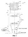
- FIG. 1is a schematic block diagram illustrating an optical system in accordance with an aspect of the present invention.
- FIG. 2is a graph illustrating sensor matching considerations in accordance with an aspect of the present invention.
- FIG. 3is a flow diagram illustrating an imaging methodology in accordance with an aspect of the present invention.
- FIG. 4is a chart illustrating exemplary performance specifications in accordance with an aspect of the present invention.
- FIG. 1illustrates an optical system 10 in accordance with an aspect of the present invention.
- the system 10includes a sensor 12 having a plurality of receptors or sensor pixels 14 .
- the sensor 12is an M by N array of sensor pixels 14 , having M rows and N columns (e.g., 640 ⁇ 480, 512 ⁇ 512, 1024 ⁇ 1280, etc.), M and N being integers respectively.
- M and Nbeing integers respectively.
- a rectangular sensor 12 having generally square pixelsis depicted, it is to be understood and appreciated that the sensor can be substantially any shape (e.g., circular, elliptical, hexagonal, rectangular, etc.).
- respective pixels 14 within the arraycan also be substantially any shape or size in accordance with an aspect of the present invention.
- the sensor 12can be substantially technology (e.g., digital sensor, analog sensor, Charge Coupled Device (CCD) sensor, CMOS sensor, Charge Injection Device (CID) sensor, an array sensor, a linear scan sensor) including one or more receptors (or pixels) 14 .
- each of the pixels 14is similarly sized or proportioned and responsive to light (e.g., visible, non-visible) received from the items under examination, as described herein.
- the sensor 12is associated with a lens network 16 , which is configured based on performance requirements of the optical system and the pitch size of sensor 12 .
- the lens network 16is operative to scale (or project) proportions (e.g., pixels 14 ) of the sensor 12 at an image plane established by the position of the sensor 12 to an object field of view 20 in accordance with an aspect of the present invention.
- the object field of view 20is related to the position of an object plane 22 that includes one or more items (not shown) under examination.
- the sensor 12As the sensor 12 receives light from the object field of view 20 , the sensor 12 provides an output 26 that can be directed to a local or remote storage such as a memory (not shown) and displayed from the memory via a computer and associated display, for example, without substantially any intervening digital processing (e.g., straight bit map from sensor memory to display), if desired. It is noted that local or remote signal processing of the image data received from the sensor 12 can also occur.
- the output 26can be converted to electronic data packets and transmitted to a remote system over a network for further analysis and/or display.
- the output 26can be stored in a local computer memory before being transmitted to a subsequent computing system for further analysis and/or display.
- the scaling (or effective projecting) of pixels 14 provided by the lens network 16is determined by a novel k-space configuration or design in accordance with an aspect of the present invention.
- the k-space design of the lens network 16promotes predetermined k-space frequencies of interest and mitigates frequencies outside the predetermined frequencies. This has the effect of a band-pass filter of the spatial frequencies within the lens network 16 and notably defines the imaging system 10 in terms of resolution rather than magnification.
- the resolution of the imaging system 10 determined by the k-space designpromotes a plurality of features in a displayed or stored image, such as having high “Effective Resolved Magnification” (a figure of merit described in following), high spatial resolution, large depth of field, larger working distances, and a unitary Modulation Transfer Function as well as other features.
- a “pitch” or spacing 28is determined between adjacent receptors 14 on the sensor 12 .
- the pitch(e.g., pixel pitch) corresponds to the center-to-center distance of adjacent receptors, indicated at 28 , which is about the size or diameter of a single receptor when the sensor includes all equally sized pixels.
- the pitch 28defines the Nyquist “cut-off” frequency band of the sensor 12 . It is this frequency band that is promoted by the k-space design, whereas other frequencies are mitigated.
- a point 30 of a desired smallest resolvable spot sizeis illustrated at the object plane 22 .
- the point 30can represent the smallest resolvable object determined by optical characteristics of the lens network 16 . That is, the lens network is configured to have optical characteristics (e.g., magnification, numerical aperture) so that each pixel 14 is matched or scaled to be about the same size in the object field of view 20 as the desired minimum resolvable spot size of the point 30 .
- optical characteristicse.g., magnification, numerical aperture
- a scaled receptor 32is depicted in front of the field of view 20 as having a size determined according to the pitch 28 of the sensor 12 , which is about the same as the point 30 .
- the lens network 16is designed to effectively reduce the size of each given receptor (e.g., pixel) 14 at the sensor 12 to be about the same size (e.g., matched in size) to the size of the point 30 , which is the minimum spot size resolvable by the system 10 .
- the point 30can be selected to a size representing the smallest resolvable object determined by optical characteristics within the lens network 16 as determined by diffraction rules (e.g., diffraction limited spot size).
- the lens network 16thus can be designed to effectively scale each pixel 14 of the sensor 12 to any size that is equal to or greater than the diffraction limited size.
- the resolvable spot sizecan be selected to provide for any desired image resolution that meets such criteria.
- the lens network 16is designed to provide the magnification to scale the pixels 14 to the object field of view 20 accordingly. This has the effect of filling the object field of view 20 with substantially all of the receptors of the sensor 12 , the respective receptors being suitably scaled to be similar in size to the point 30 , which corresponds to the desired resolvable spot size.
- the matching/mapping of sensor characteristics to the desired (e.g., smallest) resolvable object or point 30 within the object field of view 20defines the imaging system 10 in terms of absolute spatial resolution and profoundly enhances the operating performance of the system in accordance with an aspect of the present invention.
- the lens network 16includes an objective lens 34 and a secondary lens 36 .
- the objective lens 34can be set at infinite conjugate to the secondary lens 36 , with the spacing between the objective and secondary lenses being flexible.
- the lenses 34 and 36are related to each other so as to achieve a reduction from sensor space defined at the sensor array 20 to object space defined at the object plane 22 .
- substantially all of the pixels 14are projected into the object field of view 20 , which is defined by the objective lens 34 .
- the respective pixels 14are scaled through the objective lens 34 to about the dimensions of the desired minimum resolvable spot size.
- the desired resolution at the image plane 22is one micron.
- a magnification of ten timesis operative to back project a ten micron pixel to the object plane 22 and reduce it to a size of one micron.
- the reduction in size of the array 12 and associated pixels 14can be achieved by selecting the transfer lens 36 to have a focal length “D 2 ” (from the array 12 to the transfer lens 36 ) of about 150 millimeters and by selecting the objective lens to have a focal length “D 1 ” (from the objective lens 36 to the object plane 22 ) of about 15 millimeters, for example.
- the pixels 14are effectively reduced in size to about 1.0 micron per pixel, thus matching the size of the of the desired resolvable spot 30 and filling the object field of view 20 with a “virtually-reduced” array of pixels. It is to be understood and appreciated that other arrangements of one or more lenses can be employed to provide the desired magnification.
- optical mediae.g., lens network 16
- lens network 16can be designed, in accordance with an aspect of the present invention, with standard, relatively inexpensive “off-the-shelf” components having a configuration that defines that the object and image space are “unit-mapped” or “unit-matched” for substantially all image and object fields.
- the lens network 16 and, in particular the objective lens 34performs a Fourier transform of an object and an image in k-space (also referred to as “reciprocal-space”). It is this transform that is operated on for image optimization by the k-space design of the present invention.
- a small Blur-circle or airy disk at the object planeis defined by the design to match the pixels in the image plane (e.g., at the image sensor of choice) with substantially one-to-one correspondence with the airy disk and thus the Fourier transforms of pixilated arrays can be matched.
- the airy diskis scaled through the lens network 16 to be about the same size as the receptor or pixel pitch.
- the lens network 16is defined so as to construct an Intrinsic Spatial Filter (e.g., a k-space filter).
- an Intrinsic Spatial Filtere.g., a k-space filter.
- Such a design definition and implementationenables the spectral components of both the object and the image in k-space to be about the same or quantized.
- a Modulation Transfer Function (MTF)the comparison of contrast to spatial resolution
- k-spaceis defined as the region between the objective lens 34 and the secondary lens 36 . It is to be appreciated that substantially any optical media, lens type and/or lens combination that reduces, maps and/or projects the sensor array 12 to the object field of view 20 in accordance with unit or k-space mapping as described herein is within the scope of the present invention.
- conventional objective lensessized according to conventional geometric paraxial ray techniques, are generally sized according to the magnification, Numeric Aperture, focal length and other parameters provided by the objective.
- the objective lenswould be sized with a greater focal length than subsequent lenses that approach or are closer to the sensor (or eyepiece in conventional microscope) in order to provide magnification of small objects.
- the k-space design of the present inventionoperates in a manner not consistent with conventional geometrical paraxial ray design principles. That is, the objective lens 34 and the secondary lens 36 operate to provide a reduction in size of the sensor array 12 to the object field of view 20 , as demonstrated by the relationship of the lenses.
- An illumination source 40can be provided with the present invention in order that photons can be emitted from objects in the field of view 34 to enable activation of the receptors in the sensor 12 . It is noted that the present invention can potentially be employed without an illumination source 40 if potential self-luminous objects (e.g., biological specimens such as a firefly and other objects or specimens with emissive characteristics) emit enough radiation to activate the sensor 12 . It has been observed that Light Emitting Diodes provide an effective illumination source 40 in accordance with the present invention. Substantially any illumination source 40 can be applied including coherent and non-coherent sources, visible and non-visible wavelengths. However, for non-visible wavelength sources, the sensor 12 would also be suitably adapted.
- potential self-luminous objectse.g., biological specimens such as a firefly and other objects or specimens with emissive characteristics
- an infrared or ultraviolet sensor 12would be employed, respectively.
- suitable illumination sources 40can include wavelength-specific lighting, broad-band lighting, continuous lighting, strobed lighting, Kohler illumination, Abbe illumination, phase-contrast illumination, darkfield illumination, brightfield illumination, Epi illumination, and the like. Transmissive or reflective (both specular and diffuse) lighting techniques can also be applied.
- FIG. 2illustrates a graph 100 of mapping characteristics and comparison between projected pixel size on the X-axis and diffraction-limited spot resolution size “R” on the Y-axis.
- An apex 110 of the graph 100corresponds to unit mapping between projected pixel size and the diffraction limited spot size, which represents an optimum relationship between a lens network and a sensor in accordance with the present invention.
- the objective lens 34should generally not be selected such that the diffraction-limited size “R” of the smallest resolvable objects are smaller than a projected pixel size. If so, “economic waste” can occur wherein more precise information is lost (e.g., selecting an object lens more expensive than required, such as having a higher numerical aperture). This is illustrated to the right of a dividing line 120 at reference 130 depicting a projected pixel 140 larger that two smaller diffraction spots 150 . In contrast, where an objective is selected with diffraction-limited performance larger than the projected pixel size, blurring and empty magnification can occur.
- a projected pixel 170is smaller than a diffraction-limited object 180 .
- a systemcan be configured with less than optimum matching (e.g., 0.1%, 1%, 2%, 5%, 20%, 95% down from the apex 110 on the graph 100 to the left or right of the line 320 ) and still provide suitable performance in accordance with an aspect of the present invention.
- less than optimal matchingis intended to fall within the spirit and the scope of present invention.
- the diameter of the lenses in the system as illustrated in FIG. 1, for example,should be sized such that when a Fourier Transform is performed from object space to sensor space, spatial frequencies of interest that are in the band pass region described above (e.g., frequencies utilized to define the size and shape of a pixel) are substantially not attenuated. This generally implies that larger diameter lenses (e.g., about 10 to 100 millimeters) should be selected to mitigate attenuation of the spatial frequencies of interest.
- FIG. 3illustrates a methodology that can be employed to design an optical/imaging system in accordance with an aspect of the present invention.
- the methodologybegins at 200 in which an appropriate sensor array is chosen for the system.
- the sensor arrayincludes of a matrix of receptor pixels having a known pitch size, usually defined by the manufacturer.
- the sensorcan be substantially any shape (e.g., rectangular, circular, square, triangular, and so forth).
- a simple sensor of 640 ⁇ 480 pixels having a pitch size of 10 ⁇ mis chosen.
- an optical systemcan be designed for any type and/or size of sensor array in accordance with an aspect of the present invention.
- an image resolutioncorresponds to the smallest desired resolvable spot size at the image plane.
- the image resolutioncan be defined based on the application(s) for which the optical system is being designed, such as any resolution that is greater than or equal to a smallest diffraction limited size.
- resolutionbecomes a selectable design parameter that can be tailored to provide desired image resolution for virtually any type of application.
- most conventional systemstend to limit resolution according to Rayleigh diffraction, which provides that intrinsic spatial resolution of the lenses cannot exceed limits of diffraction for a given wavelength.
- magnificationis functionally related to the pixel pitch of the sensor array and the smallest resolvable spot size.
- Mmagnification
- xis the pixel pitch of the sensor array
- yis the desired image resolution (minimum spot size).
- Eq. 1provides an optical system of power ten. That is, the lens system is configured to back-project each 10 ⁇ m pixel to the object plane and reduce respective pixels to the resolvable spot size of 1 micron.
- the methodology of FIG. 3also includes a determination of a Numerical Aperture at 230 .
- the Numerical Aperture (NA)is determined according to well established diffraction rules that relate NA of the objective lens to the minimum resolvable spot size determined at 210 for the optical system.
- NA0.5 ⁇ ⁇ ⁇ y Eq . ⁇ 2
- ⁇is the wavelength of light being used in the optical system
- yis the minimum spot size (e.g., determined at 210 ).
- NAwavelength
- resolutionresolution
- the determination at 230is not limited to any particular equation but instead simply obeys known general physical laws in which NA is functionally related to the wavelength and resolution.
- the example optical system created according to the methodology of FIG. 3is to be used for microscopy.
- magnifications of many hundredsusually are required.
- the basic reason for thisis that such optics conventionally have been designed for the situation when the sensor of choice is the human eye.
- the methodology of FIG. 3designs the optical system around the sensor, which affords significant performance increases at reduced cost.
- the optical systemis designed around a discrete sensor that has known fixed dimensions.
- the methodologyprovides a far more straight-forward optical system design approach to “back-project” the sensor size onto the object plane and calculate a magnification factor.
- a second part of the methodologyhelps ensure that the optics that provide the magnification have a sufficient NA to optically resolve a spot of the same dimensions as the back-projected pixel.
- an optical system designed in accordance with an aspect of the present inventioncan utilize custom and/or off-the-shelf components.
- inexpensive opticscan be employed in accordance with an aspect of the present invention to obtain excellent results, but well-corrected microscope optics are relatively cheap. If custom-designed optics are utilized, in accordance with an aspect of the present invention, then the range of permissible magnifications and numerical apertures becomes immense, and some performance gains can be realized over the use of off-the-shelf optical components.
- FIG. 4illustrates a chart 300 of exemplary and typical performance parameters that can be achieved via the k-space design of the present invention employing standard, low-cost, and commercially available components such as dry objective lenses, a 1024 ⁇ 1280 sensor, LED illumination source wavelengths selected at about twice the wavelength of the desired resolution (e.g., for 200 nanometer resolution, 400 nanometer light source selected), and a straight bit map from sensor to image display without intervening signal processing.
- Effective Resolved Magnificationsup to about 5000 times can be achieved at a resolution of about 200 nanometers in a typical non-optimized system.
- the term “Effective Resolved Magnification”is utilized to objectively compare the relative apparent image size and Absolute Spatial Resolution of the present invention with conventional microscopic imaging systems. It is to be appreciated that the actual useful depth of field that can be achieved, in accordance with an aspect of the present invention, can be better than the conservative numbers shown in FIG. 4 .
- a plurality of related imaging applicationscan be enabled and enhanced by employing an optical/imaging system constructed in accordance with an aspect of the present invention.
- these applicationscan include but are not limited to imaging, control, inspection, microscopy and/or other analysis such as:
- Bio-medical analysise.g., cell colony counting, histology, frozen sections, cellular cytology, cellular micro-dissection, Hematology, pathology, oncology, fluorescence, interference, phase and many other clinical microscopy applications;
- Particle Sizing Applicationse.g., Pharmaceutical manufacturers, paint manufacturers, cosmetics manufacturers, food process engineering, and others
- Air quality monitoring and airborne particulate measuremente.g., clean room certification, environmental certification, and so forth
- Imaging technologiessuch as cameras, copiers, FAX machines and medical systems.
Landscapes
- Physics & Mathematics (AREA)
- General Physics & Mathematics (AREA)
- Optics & Photonics (AREA)
- Studio Devices (AREA)
Abstract
Description


Claims (22)
Priority Applications (2)
| Application Number | Priority Date | Filing Date | Title |
|---|---|---|---|
| US10/047,330US6815659B2 (en) | 2002-01-14 | 2002-01-14 | Optical system and method of making same |
| US10/830,848US20040195495A1 (en) | 2002-01-14 | 2004-04-23 | Optical system and method of making same |
Applications Claiming Priority (1)
| Application Number | Priority Date | Filing Date | Title |
|---|---|---|---|
| US10/047,330US6815659B2 (en) | 2002-01-14 | 2002-01-14 | Optical system and method of making same |
Related Child Applications (1)
| Application Number | Title | Priority Date | Filing Date |
|---|---|---|---|
| US10/830,848ContinuationUS20040195495A1 (en) | 2002-01-14 | 2004-04-23 | Optical system and method of making same |
Publications (2)
| Publication Number | Publication Date |
|---|---|
| US20030132365A1 US20030132365A1 (en) | 2003-07-17 |
| US6815659B2true US6815659B2 (en) | 2004-11-09 |
Family
ID=21948344
Family Applications (2)
| Application Number | Title | Priority Date | Filing Date |
|---|---|---|---|
| US10/047,330Expired - LifetimeUS6815659B2 (en) | 2002-01-14 | 2002-01-14 | Optical system and method of making same |
| US10/830,848AbandonedUS20040195495A1 (en) | 2002-01-14 | 2004-04-23 | Optical system and method of making same |
Family Applications After (1)
| Application Number | Title | Priority Date | Filing Date |
|---|---|---|---|
| US10/830,848AbandonedUS20040195495A1 (en) | 2002-01-14 | 2004-04-23 | Optical system and method of making same |
Country Status (1)
| Country | Link |
|---|---|
| US (2) | US6815659B2 (en) |
Cited By (6)
| Publication number | Priority date | Publication date | Assignee | Title |
|---|---|---|---|---|
| US20060082911A1 (en)* | 2004-10-07 | 2006-04-20 | Navitar, Inc. | Automated selection of optical systems |
| US20070150240A1 (en)* | 2004-10-07 | 2007-06-28 | Bridson William D | Automated selection of optical systems |
| US20070188881A1 (en)* | 2002-12-09 | 2007-08-16 | Carl Zeiss Smt Ag | Projection objective, especially for microlithography, and method for adjusting a projection objective |
| US9925017B2 (en)* | 2009-03-31 | 2018-03-27 | Brainlab Ag | Medical navigation image output comprising virtual primary images and actual secondary images |
| US10667868B2 (en) | 2015-12-31 | 2020-06-02 | Stryker Corporation | System and methods for performing surgery on a patient at a target site defined by a virtual object |
| US12408998B2 (en) | 2019-07-03 | 2025-09-09 | Stryker Corporation | Obstacle avoidance techniques for surgical navigation |
Families Citing this family (4)
| Publication number | Priority date | Publication date | Assignee | Title |
|---|---|---|---|---|
| US8648287B1 (en)* | 2005-05-27 | 2014-02-11 | Rambus Inc. | Image sensor using single photon jots and processor to create pixels |
| DE102007033737A1 (en)* | 2007-07-18 | 2009-01-22 | MAX-PLANCK-Gesellschaft zur Förderung der Wissenschaften e.V. | A method for determining a measurement based on single molecule events |
| WO2014115144A1 (en)* | 2013-01-28 | 2014-07-31 | Opgal Optronic Industries Ltd. | Enhancing infrared measurement accuracy in a specified area |
| CN113099092B (en)* | 2021-04-09 | 2022-07-08 | 凌云光技术股份有限公司 | Design method of high-performance imaging system |
Citations (40)
| Publication number | Priority date | Publication date | Assignee | Title |
|---|---|---|---|---|
| US4750022A (en) | 1985-12-27 | 1988-06-07 | Canon Kabushiki Kaisha | Optical projection system |
| US4987496A (en)* | 1989-09-18 | 1991-01-22 | Eastman Kodak Company | System for scanning halftoned images |
| US5051770A (en) | 1986-01-20 | 1991-09-24 | Scanera S.C. | Image processing device for controlling the transfer function of an optical system |
| USH1060H (en) | 1990-07-02 | 1992-05-05 | The United States Of America As Represented By The Secretary Of The Navy | Microstructure correlation counter |
| US5198653A (en) | 1992-05-04 | 1993-03-30 | Hughes Aircraft Company | Wide FOV retro-null outgoing wavefront sensor |
| EP0534768A1 (en)* | 1991-09-27 | 1993-03-31 | Texas Instruments Incorporated | Uncooled infrared detector and method for forming the same |
| US5204770A (en) | 1990-03-15 | 1993-04-20 | Nippon Telegraph And Telephone Corporation | All optical image processing and pattern recognition apparatus using stimulated photon echoes |
| US5291008A (en) | 1992-01-10 | 1994-03-01 | Welch Allyn, Inc. | Optical assembly and apparatus employing same using an aspherical lens and an aperture stop |
| US5430807A (en)* | 1992-12-14 | 1995-07-04 | Gravely Research Corporation | Variable magnification color scanning light microscope |
| US5559629A (en) | 1994-08-19 | 1996-09-24 | Tamarack Scientific Co., Inc. | Unit magnification projection system and method |
| US5666202A (en)* | 1995-08-22 | 1997-09-09 | Kyrazis; Demos | High bandwidth, dynamically rigid metrology system for the measurement and control of intelligent manufacturing processes |
| US5710430A (en)* | 1995-02-15 | 1998-01-20 | Lucent Technologies Inc. | Method and apparatus for terahertz imaging |
| US5719620A (en)* | 1993-05-05 | 1998-02-17 | Allio; Pierre | Autostereoscopic video device |
| US5737084A (en)* | 1995-09-29 | 1998-04-07 | Takaoka Electric Mtg. Co., Ltd. | Three-dimensional shape measuring apparatus |
| US5757425A (en)* | 1995-12-19 | 1998-05-26 | Eastman Kodak Company | Method and apparatus for independently calibrating light source and photosensor arrays |
| US5760398A (en)* | 1995-12-04 | 1998-06-02 | Lockheed Martin Ir Imaging Systems, Inc. | Infrared radiation detector having a reduced active area |
| US5876327A (en)* | 1996-09-03 | 1999-03-02 | Olympus Optical Co., Ltd. | Imaging apparatus for endoscopes |
| US5973844A (en) | 1996-01-26 | 1999-10-26 | Proxemics | Lenslet array systems and methods |
| US6005916A (en) | 1992-10-14 | 1999-12-21 | Techniscan, Inc. | Apparatus and method for imaging with wavefields using inverse scattering techniques |
| US6008945A (en) | 1996-09-19 | 1999-12-28 | Fergason; James L. | Display system using conjugate optics and accommodation features and method of displaying and viewing an image |
| US6020988A (en)* | 1997-08-05 | 2000-02-01 | Science Research Laboratory, Inc. | Ultra high resolution wave focusing method and apparatus and systems employing such method and apparatus |
| US6069651A (en)* | 1995-04-20 | 2000-05-30 | Olympus Optical Co., Ltd. | Imaging apparatus for endoscopes |
| US6078390A (en) | 1998-05-04 | 2000-06-20 | General Scanning, Inc. | Scanning system and method of operation for automatically setting detection sensitivity |
| US6088097A (en) | 1998-01-14 | 2000-07-11 | Uhl; Rainer | Point-scanning luminescent microscope |
| US6124974A (en) | 1996-01-26 | 2000-09-26 | Proxemics | Lenslet array systems and methods |
| US6128068A (en) | 1991-02-22 | 2000-10-03 | Canon Kabushiki Kaisha | Projection exposure apparatus including an illumination optical system that forms a secondary light source with a particular intensity distribution |
| US6178346B1 (en)* | 1998-10-23 | 2001-01-23 | David C. Amundson | Infrared endoscopic imaging in a liquid with suspended particles: method and apparatus |
| US6195213B1 (en) | 1998-06-08 | 2001-02-27 | Nikon Corporation | Projection exposure apparatus and method |
| US6248988B1 (en) | 1998-05-05 | 2001-06-19 | Kla-Tencor Corporation | Conventional and confocal multi-spot scanning optical microscope |
| US6249360B1 (en)* | 1997-04-14 | 2001-06-19 | Hewlett-Packard Company | Image scanning device and method |
| US6268918B1 (en)* | 1998-06-18 | 2001-07-31 | Minolta Co., Ltd. | Three-dimensional input device |
| US6285811B1 (en)* | 1999-02-25 | 2001-09-04 | The United States Of America As Represented By The Secretary Of The Navy | Near-field optical microscope with infrared fiber probe |
| US6344893B1 (en) | 2000-06-19 | 2002-02-05 | Ramot University Authority For Applied Research And Industrial Development Ltd. | Super-resolving imaging system |
| US6385352B1 (en)* | 1994-10-26 | 2002-05-07 | Symbol Technologies, Inc. | System and method for reading and comparing two-dimensional images |
| US20020110320A1 (en)* | 2001-02-12 | 2002-08-15 | Silicon Light Machines | Illumination system for one-dimensional spatial light modulators employing multiple light sources |
| US20020126591A1 (en)* | 1998-07-15 | 2002-09-12 | Kouichi Takamine | An optical disk and optical disk apparatus with tracks and grooves |
| US20020162973A1 (en)* | 2001-03-29 | 2002-11-07 | Cordingley James J. | Methods and systems for processing a device, methods and systems for modeling same and the device |
| US6522412B2 (en)* | 1993-12-20 | 2003-02-18 | Minolta Co., Ltd. | Measuring system with improved method of reading image data of an object |
| US6529614B1 (en)* | 1998-08-05 | 2003-03-04 | California Institute Of Technology | Advanced miniature processing handware for ATR applications |
| US6593559B2 (en)* | 2000-01-12 | 2003-07-15 | Fuji Photo Optical Co., Ltd. | Image readout apparatus and image readout method using the same |
Family Cites Families (24)
| Publication number | Priority date | Publication date | Assignee | Title |
|---|---|---|---|---|
| US3706080A (en)* | 1971-06-01 | 1972-12-12 | Honeywell Inc | Holographic optical memory having pivot lens apparatus |
| US3743379A (en)* | 1971-09-07 | 1973-07-03 | Sperry Rand Corp | Light deflector apparatus |
| US4345271A (en)* | 1979-10-24 | 1982-08-17 | Canon Kabushiki Kaisha | Television camera |
| AU2393892A (en)* | 1991-07-26 | 1993-03-02 | Accuwave Corporation | Photorefractive systems and methods |
| US5281797A (en)* | 1991-12-26 | 1994-01-25 | Hitachi, Ltd. | Short wavelength optical disk head having a changeable aperture |
| AU3371395A (en)* | 1994-09-20 | 1996-04-19 | Neopath, Inc. | Biological specimen analysis system processing integrity checking apparatus |
| US5591976A (en)* | 1994-09-26 | 1997-01-07 | The Babcock & Wilcox Company | Gamma camera system for imaging contamination |
| DK0788634T3 (en)* | 1994-10-25 | 2000-12-04 | United Parcel Service Inc | Automatic electronic camera for capturing images of labels |
| AU709025B2 (en)* | 1995-10-31 | 1999-08-19 | Benjamin T Gravely | Imaging system |
| US6177980B1 (en)* | 1997-02-20 | 2001-01-23 | Kenneth C. Johnson | High-throughput, maskless lithography system |
| US5854674A (en)* | 1997-05-29 | 1998-12-29 | Optical Specialties, Inc. | Method of high speed, high detection sensitivity inspection of repetitive and random specimen patterns |
| US6388788B1 (en)* | 1998-03-16 | 2002-05-14 | Praelux, Inc. | Method and apparatus for screening chemical compounds |
| FR2776067B1 (en)* | 1998-03-16 | 2000-06-23 | Commissariat Energie Atomique | SYSTEM FOR DETERMINING AND QUANTIFYING THE ALIGNMENT OF AN OBJECT WITH A COUPLING OPTICAL AND A SHOOTING DEVICE |
| AU4953599A (en)* | 1998-10-05 | 2000-04-26 | University Of Maryland | Imaging using spatial frequency filtering and masking |
| US6282264B1 (en)* | 1999-10-06 | 2001-08-28 | Hologic, Inc. | Digital flat panel x-ray detector positioning in diagnostic radiology |
| US6851851B2 (en)* | 1999-10-06 | 2005-02-08 | Hologic, Inc. | Digital flat panel x-ray receptor positioning in diagnostic radiology |
| US6777934B2 (en)* | 1999-12-08 | 2004-08-17 | Hitachi Medical Corporation | Magnetic resonance imaging method and apparatus |
| JP3942785B2 (en)* | 2000-01-26 | 2007-07-11 | エスアイアイ・ナノテクノロジー株式会社 | Optical fiber probe, cantilever with microscopic aperture, and method for forming the aperture |
| US6324249B1 (en)* | 2001-03-21 | 2001-11-27 | Agilent Technologies, Inc. | Electronic planar laminography system and method |
| US7338168B2 (en)* | 2001-07-06 | 2008-03-04 | Palantyr Research, Llc | Particle analyzing system and methodology |
| US7151246B2 (en)* | 2001-07-06 | 2006-12-19 | Palantyr Research, Llc | Imaging system and methodology |
| US6884983B2 (en)* | 2002-06-10 | 2005-04-26 | Palantyr Research, Llc | Imaging system for examining biological material |
| US6664528B1 (en)* | 2001-07-06 | 2003-12-16 | Palantyr Research, Llc | Imaging system and methodology employing reciprocal space optical design |
| US6813008B2 (en)* | 2002-06-10 | 2004-11-02 | Palantyr Research, Llc | Microdissection optical system |
- 2002
- 2002-01-14USUS10/047,330patent/US6815659B2/ennot_activeExpired - Lifetime
- 2004
- 2004-04-23USUS10/830,848patent/US20040195495A1/ennot_activeAbandoned
Patent Citations (40)
| Publication number | Priority date | Publication date | Assignee | Title |
|---|---|---|---|---|
| US4750022A (en) | 1985-12-27 | 1988-06-07 | Canon Kabushiki Kaisha | Optical projection system |
| US5051770A (en) | 1986-01-20 | 1991-09-24 | Scanera S.C. | Image processing device for controlling the transfer function of an optical system |
| US4987496A (en)* | 1989-09-18 | 1991-01-22 | Eastman Kodak Company | System for scanning halftoned images |
| US5204770A (en) | 1990-03-15 | 1993-04-20 | Nippon Telegraph And Telephone Corporation | All optical image processing and pattern recognition apparatus using stimulated photon echoes |
| USH1060H (en) | 1990-07-02 | 1992-05-05 | The United States Of America As Represented By The Secretary Of The Navy | Microstructure correlation counter |
| US6128068A (en) | 1991-02-22 | 2000-10-03 | Canon Kabushiki Kaisha | Projection exposure apparatus including an illumination optical system that forms a secondary light source with a particular intensity distribution |
| EP0534768A1 (en)* | 1991-09-27 | 1993-03-31 | Texas Instruments Incorporated | Uncooled infrared detector and method for forming the same |
| US5291008A (en) | 1992-01-10 | 1994-03-01 | Welch Allyn, Inc. | Optical assembly and apparatus employing same using an aspherical lens and an aperture stop |
| US5198653A (en) | 1992-05-04 | 1993-03-30 | Hughes Aircraft Company | Wide FOV retro-null outgoing wavefront sensor |
| US6005916A (en) | 1992-10-14 | 1999-12-21 | Techniscan, Inc. | Apparatus and method for imaging with wavefields using inverse scattering techniques |
| US5430807A (en)* | 1992-12-14 | 1995-07-04 | Gravely Research Corporation | Variable magnification color scanning light microscope |
| US5719620A (en)* | 1993-05-05 | 1998-02-17 | Allio; Pierre | Autostereoscopic video device |
| US6522412B2 (en)* | 1993-12-20 | 2003-02-18 | Minolta Co., Ltd. | Measuring system with improved method of reading image data of an object |
| US5559629A (en) | 1994-08-19 | 1996-09-24 | Tamarack Scientific Co., Inc. | Unit magnification projection system and method |
| US6385352B1 (en)* | 1994-10-26 | 2002-05-07 | Symbol Technologies, Inc. | System and method for reading and comparing two-dimensional images |
| US5710430A (en)* | 1995-02-15 | 1998-01-20 | Lucent Technologies Inc. | Method and apparatus for terahertz imaging |
| US6069651A (en)* | 1995-04-20 | 2000-05-30 | Olympus Optical Co., Ltd. | Imaging apparatus for endoscopes |
| US5666202A (en)* | 1995-08-22 | 1997-09-09 | Kyrazis; Demos | High bandwidth, dynamically rigid metrology system for the measurement and control of intelligent manufacturing processes |
| US5737084A (en)* | 1995-09-29 | 1998-04-07 | Takaoka Electric Mtg. Co., Ltd. | Three-dimensional shape measuring apparatus |
| US5760398A (en)* | 1995-12-04 | 1998-06-02 | Lockheed Martin Ir Imaging Systems, Inc. | Infrared radiation detector having a reduced active area |
| US5757425A (en)* | 1995-12-19 | 1998-05-26 | Eastman Kodak Company | Method and apparatus for independently calibrating light source and photosensor arrays |
| US5973844A (en) | 1996-01-26 | 1999-10-26 | Proxemics | Lenslet array systems and methods |
| US6124974A (en) | 1996-01-26 | 2000-09-26 | Proxemics | Lenslet array systems and methods |
| US5876327A (en)* | 1996-09-03 | 1999-03-02 | Olympus Optical Co., Ltd. | Imaging apparatus for endoscopes |
| US6008945A (en) | 1996-09-19 | 1999-12-28 | Fergason; James L. | Display system using conjugate optics and accommodation features and method of displaying and viewing an image |
| US6249360B1 (en)* | 1997-04-14 | 2001-06-19 | Hewlett-Packard Company | Image scanning device and method |
| US6020988A (en)* | 1997-08-05 | 2000-02-01 | Science Research Laboratory, Inc. | Ultra high resolution wave focusing method and apparatus and systems employing such method and apparatus |
| US6088097A (en) | 1998-01-14 | 2000-07-11 | Uhl; Rainer | Point-scanning luminescent microscope |
| US6078390A (en) | 1998-05-04 | 2000-06-20 | General Scanning, Inc. | Scanning system and method of operation for automatically setting detection sensitivity |
| US6248988B1 (en) | 1998-05-05 | 2001-06-19 | Kla-Tencor Corporation | Conventional and confocal multi-spot scanning optical microscope |
| US6195213B1 (en) | 1998-06-08 | 2001-02-27 | Nikon Corporation | Projection exposure apparatus and method |
| US6268918B1 (en)* | 1998-06-18 | 2001-07-31 | Minolta Co., Ltd. | Three-dimensional input device |
| US20020126591A1 (en)* | 1998-07-15 | 2002-09-12 | Kouichi Takamine | An optical disk and optical disk apparatus with tracks and grooves |
| US6529614B1 (en)* | 1998-08-05 | 2003-03-04 | California Institute Of Technology | Advanced miniature processing handware for ATR applications |
| US6178346B1 (en)* | 1998-10-23 | 2001-01-23 | David C. Amundson | Infrared endoscopic imaging in a liquid with suspended particles: method and apparatus |
| US6285811B1 (en)* | 1999-02-25 | 2001-09-04 | The United States Of America As Represented By The Secretary Of The Navy | Near-field optical microscope with infrared fiber probe |
| US6593559B2 (en)* | 2000-01-12 | 2003-07-15 | Fuji Photo Optical Co., Ltd. | Image readout apparatus and image readout method using the same |
| US6344893B1 (en) | 2000-06-19 | 2002-02-05 | Ramot University Authority For Applied Research And Industrial Development Ltd. | Super-resolving imaging system |
| US20020110320A1 (en)* | 2001-02-12 | 2002-08-15 | Silicon Light Machines | Illumination system for one-dimensional spatial light modulators employing multiple light sources |
| US20020162973A1 (en)* | 2001-03-29 | 2002-11-07 | Cordingley James J. | Methods and systems for processing a device, methods and systems for modeling same and the device |
Non-Patent Citations (6)
| Title |
|---|
| "Using your microscope, high magnifications with an oil-immersion objective," riberuet. 1999-2000. |
| Casasesnt, David, "Performing Image Analysis With Optical Pattern Recognition," The Photonics Design and Applications Handbook, 1998, pp. 158-161. |
| Holst, Gerald C., "Image Quality: Does Your Detector Match Your Optics? Understanding the term "resolution" for both optics and detectors provides a solid basis for designing imaging systems." Photonics Spectra, Jan. 1999, pp. 144-146. |
| International Search Report dated Nov. 12, 2002 in PCT Application No. PCT/US02/21392 filed Jul. 3, 2002. |
| Melles Griot, Optical Systems, Machine Vision Product Guide, USA, 1998. |
| Mukundakrishnan, Bharath, "Design for Visually Servoed Microassembly," Advanced Microsystems Laboratory, Department of Mechanical Engineering, University of Minnesota 2000. |
Cited By (11)
| Publication number | Priority date | Publication date | Assignee | Title |
|---|---|---|---|---|
| US20070188881A1 (en)* | 2002-12-09 | 2007-08-16 | Carl Zeiss Smt Ag | Projection objective, especially for microlithography, and method for adjusting a projection objective |
| US7310187B2 (en)* | 2002-12-09 | 2007-12-18 | Carl Zeiss Smt Ag | Projection objective, especially for microlithography, and method for adjusting a projection objective |
| US20060082911A1 (en)* | 2004-10-07 | 2006-04-20 | Navitar, Inc. | Automated selection of optical systems |
| US7149662B2 (en) | 2004-10-07 | 2006-12-12 | Navitar, Inc. | Automated selection of optical systems |
| US20070150240A1 (en)* | 2004-10-07 | 2007-06-28 | Bridson William D | Automated selection of optical systems |
| US9925017B2 (en)* | 2009-03-31 | 2018-03-27 | Brainlab Ag | Medical navigation image output comprising virtual primary images and actual secondary images |
| US10667868B2 (en) | 2015-12-31 | 2020-06-02 | Stryker Corporation | System and methods for performing surgery on a patient at a target site defined by a virtual object |
| US11103315B2 (en) | 2015-12-31 | 2021-08-31 | Stryker Corporation | Systems and methods of merging localization and vision data for object avoidance |
| US11806089B2 (en) | 2015-12-31 | 2023-11-07 | Stryker Corporation | Merging localization and vision data for robotic control |
| US12364548B2 (en) | 2015-12-31 | 2025-07-22 | Stryker Corporation | Systems and methods for comparing localization and vision data to identify an avoidance region |
| US12408998B2 (en) | 2019-07-03 | 2025-09-09 | Stryker Corporation | Obstacle avoidance techniques for surgical navigation |
Also Published As
| Publication number | Publication date |
|---|---|
| US20040195495A1 (en) | 2004-10-07 |
| US20030132365A1 (en) | 2003-07-17 |
Similar Documents
| Publication | Publication Date | Title |
|---|---|---|
| US6664528B1 (en) | Imaging system and methodology employing reciprocal space optical design | |
| US6884983B2 (en) | Imaging system for examining biological material | |
| US7105795B2 (en) | Imaging system, methodology, and applications employing reciprocal space optical design | |
| US7288751B2 (en) | Imaging system, methodology, and applications employing reciprocal space optical design | |
| US7439478B2 (en) | Imaging system, methodology, and applications employing reciprocal space optical design having at least one pixel being scaled to about a size of a diffraction-limited spot defined by a microscopic optical system | |
| JP6655121B2 (en) | Optical measurement method | |
| CA2453049C (en) | Imaging system and methodology employing reciprocal space optical design | |
| Dan et al. | Structured illumination microscopy for super-resolution and optical sectioning | |
| US9360665B2 (en) | Confocal optical scanner | |
| US7132636B1 (en) | Imaging system and methodology employing reciprocal space optical design | |
| US6813008B2 (en) | Microdissection optical system | |
| US20050024720A1 (en) | Imaging system, methodology, and applications employing reciprocal space optical design | |
| US6872930B2 (en) | Imaging system and methodology employing reciprocal space optical design | |
| AU2002322410A1 (en) | Imaging system and methodology employing reciprocal space optical design | |
| US6815659B2 (en) | Optical system and method of making same | |
| Yu et al. | Microlens array snapshot hyperspectral microscopy system for the biomedical domain | |
| US20150085360A1 (en) | Confocal microscope | |
| Girkin | A practical guide to optical microscopy | |
| Wilson | Three‐dimensional imaging in confocal systems | |
| Fennell et al. | Design, development, and performance comparison of wide field lensless and lens-based optical systems for point-of-care biological applications | |
| WO2010042576A1 (en) | A system and method for adjusting a beam expander in an imaging system | |
| Vila et al. | Ultra-compact and large field-of-view nano-illumination light microscope based on an array of organic light-emitting diodes | |
| WO2003005446A1 (en) | Imaging system and methodology employing reciprocal space optical design | |
| Macedo et al. | Development and assessment of image reconstruction algorithms using a low-cost bench-microscope based on a linear CMOS image sensor |
Legal Events
| Date | Code | Title | Description |
|---|---|---|---|
| AS | Assignment | Owner name:BORTNICK, DANIEL B., OHIO Free format text:ASSIGNMENT OF ASSIGNORS INTEREST;ASSIGNOR:CARTLIDGE, ANDREW G.;REEL/FRAME:012517/0685 Effective date:20020110 Owner name:PALANTYR RESEARCH, LLC, OHIO Free format text:ASSIGNMENT OF ASSIGNORS INTEREST;ASSIGNOR:CARTLIDGE, ANDREW G.;REEL/FRAME:012517/0685 Effective date:20020110 Owner name:TUROCY, GREGORY, OHIO Free format text:ASSIGNMENT OF ASSIGNORS INTEREST;ASSIGNOR:CARTLIDGE, ANDREW G.;REEL/FRAME:012517/0685 Effective date:20020110 Owner name:ANGKOR TECHNOLOGY, LLP, OHIO Free format text:ASSIGNMENT OF ASSIGNORS INTEREST;ASSIGNOR:CARTLIDGE, ANDREW G.;REEL/FRAME:012517/0685 Effective date:20020110 Owner name:AMIN, HIMANSHU S., OHIO Free format text:ASSIGNMENT OF ASSIGNORS INTEREST;ASSIGNOR:CARTLIDGE, ANDREW G.;REEL/FRAME:012517/0685 Effective date:20020110 | |
| STCF | Information on status: patent grant | Free format text:PATENTED CASE | |
| CC | Certificate of correction | ||
| FPAY | Fee payment | Year of fee payment:4 | |
| FPAY | Fee payment | Year of fee payment:8 | |
| AS | Assignment | Owner name:PIXEL MATCHED HOLDINGS LLC, OHIO Free format text:ASSIGNMENT OF ASSIGNORS INTEREST;ASSIGNORS:PALANTYR RESEARCH, LLC;AMIN, HIMANSHU S.;ANGKOR TECHNOLOGY, LLP;AND OTHERS;REEL/FRAME:037060/0667 Effective date:20151029 | |
| FPAY | Fee payment | Year of fee payment:12 |