US6815358B2 - Electron beam lithography method for plating sub-100 nm trenches - Google Patents
Electron beam lithography method for plating sub-100 nm trenchesDownload PDFInfo
- Publication number
- US6815358B2 US6815358B2US10/108,309US10830902AUS6815358B2US 6815358 B2US6815358 B2US 6815358B2US 10830902 AUS10830902 AUS 10830902AUS 6815358 B2US6815358 B2US 6815358B2
- Authority
- US
- United States
- Prior art keywords
- layer
- dissolution
- undercoat
- resist layer
- narrow trench
- Prior art date
- Legal status (The legal status is an assumption and is not a legal conclusion. Google has not performed a legal analysis and makes no representation as to the accuracy of the status listed.)
- Expired - Fee Related, expires
Links
Images


Classifications
- G—PHYSICS
- G11—INFORMATION STORAGE
- G11B—INFORMATION STORAGE BASED ON RELATIVE MOVEMENT BETWEEN RECORD CARRIER AND TRANSDUCER
- G11B5/00—Recording by magnetisation or demagnetisation of a record carrier; Reproducing by magnetic means; Record carriers therefor
- G11B5/127—Structure or manufacture of heads, e.g. inductive
- G11B5/31—Structure or manufacture of heads, e.g. inductive using thin films
- G11B5/3109—Details
- G11B5/3116—Shaping of layers, poles or gaps for improving the form of the electrical signal transduced, e.g. for shielding, contour effect, equalizing, side flux fringing, cross talk reduction between heads or between heads and information tracks
- G—PHYSICS
- G11—INFORMATION STORAGE
- G11B—INFORMATION STORAGE BASED ON RELATIVE MOVEMENT BETWEEN RECORD CARRIER AND TRANSDUCER
- G11B5/00—Recording by magnetisation or demagnetisation of a record carrier; Reproducing by magnetic means; Record carriers therefor
- G11B5/127—Structure or manufacture of heads, e.g. inductive
- G11B5/31—Structure or manufacture of heads, e.g. inductive using thin films
- G11B5/3163—Fabrication methods or processes specially adapted for a particular head structure, e.g. using base layers for electroplating, using functional layers for masking, using energy or particle beams for shaping the structure or modifying the properties of the basic layers
- H—ELECTRICITY
- H01—ELECTRIC ELEMENTS
- H01F—MAGNETS; INDUCTANCES; TRANSFORMERS; SELECTION OF MATERIALS FOR THEIR MAGNETIC PROPERTIES
- H01F41/00—Apparatus or processes specially adapted for manufacturing or assembling magnets, inductances or transformers; Apparatus or processes specially adapted for manufacturing materials characterised by their magnetic properties
- H01F41/32—Apparatus or processes specially adapted for manufacturing or assembling magnets, inductances or transformers; Apparatus or processes specially adapted for manufacturing materials characterised by their magnetic properties for applying conductive, insulating or magnetic material on a magnetic film, specially adapted for a thin magnetic film
- H01F41/34—Apparatus or processes specially adapted for manufacturing or assembling magnets, inductances or transformers; Apparatus or processes specially adapted for manufacturing materials characterised by their magnetic properties for applying conductive, insulating or magnetic material on a magnetic film, specially adapted for a thin magnetic film in patterns, e.g. by lithography
- G—PHYSICS
- G11—INFORMATION STORAGE
- G11B—INFORMATION STORAGE BASED ON RELATIVE MOVEMENT BETWEEN RECORD CARRIER AND TRANSDUCER
- G11B5/00—Recording by magnetisation or demagnetisation of a record carrier; Reproducing by magnetic means; Record carriers therefor
- G11B5/127—Structure or manufacture of heads, e.g. inductive
- G11B5/187—Structure or manufacture of the surface of the head in physical contact with, or immediately adjacent to the recording medium; Pole pieces; Gap features
- G11B5/1871—Shaping or contouring of the transducing or guiding surface
Definitions
- This inventionrelates generally to lithography methods for printing and plating isolated narrow trenches with feature dimensions less than 100 nm, and more particularly, to a bi-layer lithographic method utilizing a thin undercoat dissolution layer beneath a resist layer.
- the areal density of magnetic disk storagehas sustained annual increases of 100% during the last five years, largely due to shrinking dimensions in the read/write head. From a process perspective, this requires that the width of the critical read sensor and writer pole tip decrease by 20% to 30% each year.
- a trackpitchshould be approximately 160 nm.
- the trackwidthshould be approximately 130 nm.
- the critical dimension (“CD”)needs to be pushed down to 30 nm.
- the write pole tipto have an aspect ratio of between 7:1 to 10:1, which is achieved by electroplating high magnetic moment materials into a narrow trench printed in the resist.
- the aspect ratiois defined as the height divided by the width.
- the widthis also referred to as the critical dimension, CD.
- the inventionprovides a bi-layer lithography method for printing and plating sub-100 nm narrow trenches having a high aspect ratio.
- the methodcan include providing a thin layer of polymer as an undercoat dissolution layer disposed intermediate a substrate and a resist layer.
- the substratecan normally be coated with a non-magnetic seed layer prior to deposition of the undercoat layer.
- the resist and undercoat layerare exposed to a radiation source capable of sub-100 nm resolution, such as an electron beam, to pattern the narrow trench and an aqueous developer solution is then used to define the narrow trench.
- the exposed portions of the resist and undercoat dissolution layerare thereafter dissolved in a standard aqueous base developer solution to define the narrow trench.
- the narrow trenchcan then be electroplated with a high magnetic moment material to form, for example, a pole tip of a magnetic write head.
- the undercoat materialcan be more completely cleared off the seed layer by the developer solution.
- the sides of the narrow trenchwill be generally vertical, particularly at the base of the narrow trench, since relatively little of the undercoat material remains on the seed layer.
- Additional stepscan include one or more of the following: baking the undercoat layer after it has been deposited on the substrate/seed layer; baking the resist layer after it has been deposited on the undercoat layer; and baking both layers after e-beam exposure.
- the baking time and baking temperaturecan be calculated to control various properties of the process, particularly the dissolution rate of the undercoat layer.
- FIGS. 1-3illustrate a conventional process for patterning a narrow trench
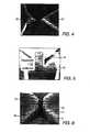
- FIG. 4is a pictorial representation of a scanning electron microscopy (“SEM”) image of a 90 nm pole tip patterned using the conventional process shown in FIGS. 1-3;
- SEMscanning electron microscopy
- FIG. 5is a pictorial representation of a focus ion beam (“FIB”) cross sectional image of a 120 nm plated pole tip patterned using the conventional process shown in FIGS. 1-3;
- FIBfocus ion beam
- FIG. 6is a pictorial representation of an SEM image of the 120 nm trench patterned using the conventional process shown in FIGS. 1-3 before it was plated to form the pole tip shown in FIG. 5;
- FIGS. 7-10illustrate a certain embodiment of a method for patterning a sub-100 nm narrow trench
- FIG. 11is a graph of dissolution rate vs. bake temperature for PMGI
- FIG. 12is a pictorial representation of an atomic force microscopy (“AFM”) image of the surface of a seed layer
- FIGS. 13-14are pictorial representations of AFM images showing the seed layer in FIG. 12 after deposition, exposure, and development of a resist layer, with and without an undercoat dissolution layer, respectively;
- FIG. 15is a pictorial representation of a FIB cross sectional image of a 90 nm pole tip patterned using the conventional process shown in FIGS. 1-3;
- FIGS. 16-17are pictorial representations of FIB cross sectional images of a 90 nm pole tip patterned using the process illustrated in FIGS. 7-10;
- FIG. 18is a pictorial representation of an FIB image of the plated pole tip shown in FIG. 15;
- FIGS. 19-20are pictorial representations of FIB images of the plated pole tips shown in FIGS. 16-17;
- FIGS. 21-22are pictorial representations of FIB cross sectional images of very narrow pole tips successfully printed and plated using the process illustrated in FIGS. 7 - 10 .
- FIGS. 1 through 3A conventional electron beam, or “e-beam,” lithographic process for patterning a sub-100 nm trench is illustrated in FIGS. 1 through 3.
- the pole tipis created by electro-deposition of high magnetic moment material into the narrow trench.
- the conventional processconsists of providing a substrate 30 on which a resist layer 33 is deposited.
- the substrate 30is first coated with a non-magnetic seed layer 36 prior to deposition of the resist layer 33 .
- the substrate 30can be AlTiC, an alloy of aluminum, titanium, and carbon.
- the seed layer 36can be nickel vanadium (“NiV”).
- Alternative seed layer materialscan include nickel phosphorus, nickel molybdenum, nickel chromium, nickel tungsten, gold, and copper.
- the resist layer 33can be, for example, a deep ultravoid (“DUV”) resist layer, such as UV113, which can be obtained from industry suppliers such as Hoechst Celanese, Sumitomo, and Shipley.
- the DUV resist layer 33is exposed to an electron beam to pattern a narrow trench.
- a “pattern” of the trenchis created in the resist layer 33 by the electron beam.
- the resist layer 33is developed using an appropriate solution to define, or “print,” the narrow trench 39 , as shown in FIG. 3 .
- the narrow trench 39is ready to be plated, such as by electro-deposition, with a high magnetic moment material to form, for example, a pole tip.
- the plating materialis a high magnetic moment material, for example CoNiFe.
- the remaining resist layer 33can be removed by an appropriate strip solution, for example NMP. If plating is successful, only a plated pole tip will remain.
- FIG. 4there is shown a sub-100 nm pole tip 42 is shown which was printed using a conventional electron beam lithography process such as described above.
- a narrow trench having a CD of about 90 nmwas printed using a 0.65 ⁇ m thick DUV resist layer, giving an aspect ratio of approximately 7.3:1.
- the attempt to electroplate the narrow trenchfailed, as indicated by the gap in the middle of the pole tip 42 .
- FIG. 5shows a printed and plated 120 nm pole tip 45 , demarcated generally by a dotted rectangular outline, which reveals an undercut profile 48 , i.e., rounded base, at the bottom of the pole tip 45 .
- undercutrefers to the side walls of the pole tip not being vertical at the bottom. This condition tends to indicate that the prior inability to successfully plate sub-100 nm narrow trenches by electro-deposition methods may result from such an undercut profile 48 created at the bottom of the plated pole tip 45 .
- the undercut profile 48may prevent the plating material from attaching to the seed layer, or substrate, at the bottom of the trench.
- a close examination of the bottom of the corresponding patterned resist 51shown in FIG.
- the failure to completely clear the resist 51 from the bottom 57 of the narrow trench 60 during the developing processcan potentially be due to a couple of reasons.
- the first such reasoncan be that the resist 51 simply tends to adhere to the seed layer 66 , and is thus difficult to completely remove.
- the second reasonwhich may also be related to the first reason, can be that the narrowness of the trench 60 limits the ability of the aqueous base developing solution, or a sufficient amount thereof, to penetrate all the way to the bottom 57 of the trench 60 to sufficiently clear away all of the resist 51 .
- the second reasonregards the physics of diffusion of liquids into a very narrow trench.
- the width of the trench 60is so small, i.e., less than 100 nm, it can be difficult for a sufficient amount of fresh development solution liquid to diffuse into the trench 60 and thereby penetrate all the way to the bottom 57 of the trench 60 to completely remove all of the resist 51 from the seed layer 66 .
- the methodcan include employing a thin layer of polymer as an undercoat dissolution layer 70 disposed intermediate the substrate 73 and the resist layer 76 .
- the undercoat dissolution layer 70will normally be disposed on a non-magnetic seed layer 79 with which the substrate 70 is normally first coated with prior to deposition of the undercoat dissolution layer 70 .
- the undercoat dissolution layer 70can be dissolvable in a standard aqueous base developer solution, such as tetra-methyl ammonium hydroxide (“TMAH”).
- the undercoat dissolution layer 70will preferably meet three criteria. First, the dissolution layer 70 should have a dissolution rate greater than the dissolution rate of the resist layer 76 , i.e., the dissolution layer should be quickly and easily dissolved compared to the resist layer 76 during the developing process. Second, ideally, the dissolution rate of the material comprising the undercoat dissolution layer 70 will be temperature dependent. This will permit the dissolution rate of the undercoat layer 70 to be tunable by control of the bake temperature. Third, and lastly, use of the undercoat dissolution layer 70 must enable the printing and plating of a sub-100 nm narrow trench 82 wherein the bottom 85 of the trench 82 is completely clear of resist 76 .
- a preferred undercoat dissolution layer 70is be polymethylglutarimide (“PMGI”), which can be purchased from MicroChem Corporation. PMGI is also commercially known as SAL-110 or LOL-1000 when purchased from the Shipley Company. The difference between SAL-110 and LOL-1000 is its molecular weight (Mw). The Mw of SAL-110 is 110,000 Daltons and the Mw of LOL-1000 is approximately 20,000 Daltons.
- PMGIis the best known material for use as the undercoat dissolution layer
- other materialswhich have similar properties, e.g., a dissolution rate greater than the resist layer 76 , temperature dependent dissolution rate, etc., such that sub-100 nm trenches can be successfully plated, could be substituted for use as the undercoat dissolution layer in light of the teachings of the invention as disclosed herein.
- the methodcan generally comprise the following steps: (1) providing a thin PMGI undercoat dissolution layer 70 on a seed layer 79 (or simply on a substrate 73 ), as shown in FIG. 7; (2) providing a resist layer 76 on top of the PMGI layer 70 , as shown in FIG. 8; (3) exposing the resist 76 and PMGI 70 layers to a radiation source capable of sub-100 nm resolution to pattern a narrow trench, as shown in FIG. 9; (4) developing the exposed resist 76 and PMGI 70 layers to print the narrow trench 82 , as shown in FIG.
- the PMGI undercoat layer 70is generally completely removed from the bottom 85 of the trench 82 by the development solution so that the side walls 88 of the trench 82 are generally vertical, especially at the bottom 85 ; and (5) plating the trench 82 with a high magnetic moment material to form a pole tip (not shown).
- the thickness of the thin PMGI layer 70can be from about 10 nm to about 50 nm, and can also be related to the thickness of the resist layer 76 .
- the thickness of the resist layer 76is also variable, as is the width of the trench 82 , since the combination of these dimensions define the aspect ratio of the trench 82 .
- Electron beam lithographycan be utilized in this embodiment, but it is to be understood that other radiation sources capable of sub-100 nm resolution could be utilized.
- radiation sources used for lithographycan be classified into photon lithography (optical, UV, deep UV), electron beam lithography, and ion beam lithography. Resolution is limited by the wavelength of the radiation source. Consequently, lithography processes using very short wavelength radiation sources are preferred. Some of the preferred lithography processes for making sub-100 nm features include electron beam lithography, X-ray lithography, extreme ultraviolet (EUV) lithography, and ion-beam lithography.
- EUVextreme ultraviolet
- FIG. 1Other embodiments of the invention can comprise one or more of the following additional steps.
- baking the PMGI layer 70 after it has been deposited; baking the resist layer 76 after it has been deposited on the PMGI layer 70 ; and baking the resist 76 and PMGI 70 layers after patterning the narrow trench 82 .
- the PMGI dissolution rateis temperature dependent, using different temperatures provides control over the dissolution rate of PMGI.
- the resist layer 76is initially baked immediately after being coated on the PMGI layer 70 . This process is commonly referred to as “post apply bake” (PAB).
- PABpost apply bake
- the process used to deposit the resist layer 76 on the PMGI layer 70can result in the resist layer 76 containing up to 15% residual solvent.
- the PAB stepis used to remove this residual solvent prior to electron beam exposure.
- the second baking processis performed after e-beam exposure, and is referred to as “post exposure bake” (PEB).
- PEBis normally performed immediately after e-beam exposure.
- chemical reactionsoccur when the wafer is baked above a given chemical activation energy.
- PEBis used to induce new reactions that aid in developing subsequent relief images in the resist layer 76 .
- LDD-26Wis a basic salt TMAH with a surfactant included.
- TMAHcan include potassium hydroxide (“KOH”) and, a relatively weaker solution known as AZ developer (consisting of sodium hydroxide buffered with a phosphoric acid, trisodium salt and silicic acid).
- KOHpotassium hydroxide
- AZ developerrelatively weaker solution
- various types of developers, as well as variable strength formulations of the samee.g., solution diluted by H 2 O
- Such developer solutionscan be obtained from industry suppliers such as Hoechst Celanese, Sumitomo, and Shipley.
- the bake temperature, PEB or PAB, and the bake timecan be manipulated to control various properties of the process.
- the dissolution rate of PMGIhas been found to vary as a function of the bake temperature.
- the dissolution rate of PMGIdecreases. Consequently, if the bake temperature is too high, an insufficient amount of the PMGI layer 70 can be dissolved, thus leaving the same type of foot at the base of the side walls 88 of the narrow trench 82 as described previously.
- the bake temperatureis too low, too much of the exposed PMGI layer 70 may be dissolved, thus creating an undercut below the side walls 88 of the trench 82 .
- FIG. 12there is shown the surface of a seed layer 90 , for example NiV, on a substrate, which can be AlTiC.
- the surface of the seed layer 90consists primarily of approximately 10 nm grains. Additional images of an area near a printed narrow trench (the trench itself is not shown in the figures) are provided in FIGS. 13 and 14. These images suggest that a method using a PMGI undercoat layer can clear resist residual at the bottom of a narrow trench.
- FIG. 13shows the topography of an area of a seed layer 96 near the bottom of a narrow trench that was printed in accordance with a method according to the invention as described in FIGS.
- the seed layer 96was coated with a PMGI undercoat layer, and a UV113 resist layer.
- the imagereveals that the surface of the seed layer 96 is generally smooth and clear, with very similar structure, i.e., lots of approximately 10 nm grains, as that of the surface of the bare seed layer 90 shown in FIG. 12 .
- a totally different featureis observed on the surface of the seed layer 99 in FIG. 14 .
- the trenchwas patterned and printed according to the conventional process described in FIGS. 1 through 3, i.e., the seed layer 99 was coated with a UV113 resist layer, but no PMGI undercoat layer.
- the seed layer 99has a rougher surface compared to either the bare seed layer 90 or the seed layer 96 , which had a PMGI undercoat layer.
- Data from grain size analysis of the image in FIG. 14indicates that many “bulk-like” clusters with dimensions of roughly 20 nm to 60 nm remain on the surface of the seed layer 99 .
- the datasuggests that in a process which does not utilize an undercoat dissolution layer, the resist does not completely clear the bottom of the narrow trench on the nanometer scale.
- some resist residuals on the scale of tens of nanometersadhere to the surface of the seed layer 99 . It can be very difficult, if not impossible, to completely clear every trace of the small resist residuals using the conventional develop process due to the extremely narrow width and high aspect ratio of the trenches being patterned and printed.
- FIGS. 15 through 17which providing a direct comparison of the PMGI undercoat layer effect on plated 90 nm top poles.
- FIG. 15shows a 90 nm top pole 102 which was printed and plated, unsuccessfully (see FIG. 18 ), without using a PMGI undercoat layer process.
- FIGS. 16 and 17show 90 nm top poles 105 , 108 , respectively, which were printed and successfully plated using a PMGI undercoat layer process.
- the top pole 105 in FIG. 16was plated with NiFe whereas the top pole 108 in FIG. 17 was plated with CoNiFe.
- FIGS. 18 through 20show the side walls of the plated pole tips in FIGS. 15 through 17, respectively.
- FIGS.more clearly illustrate the benefits of the PMGI undercoat layer process.
- the pole tip 102 printed without using a PMGI undercoat layer processcould not be successfully plated, in this case with CoNiFe, as indicated by the break in the middle of the pole tip 102 .
- the pole tips 105 and 108 in FIGS. 19 and 20were successfully plated with NiFe and CoNiFe, respectively.
- the PMGI undercoat layer processalso results in generally smooth side walls on both the NiFe plated pole tip 105 and the CoNiFe plated pole tip 108 .
- FIGS. 21 and 22further demonstrate the success of utilizing a PMGI undercoat dissolution layer.
- the use of the PMGI undercoat layerenables printing and plating narrow trenches having a critical dimension far less than 100 nm.
- FIG. 21, for example,shows a pole tip 111 having a CD of 30 nm and an aspect ratio of 8.3:1.
- FIG. 22shows an even smaller pole tip 114 , having a CD of 22 nm and an aspect ratio of 4.5:1.
- both pole tips 111 , 114were successfully plated with NiFe.
- Alternative high magnetic moment materialscould also be utilized in addition to NiFe.
- the 22 nm pole tip 114is believed to be the narrowest electro-deposited pole tip ever fabricated.
Landscapes
- Engineering & Computer Science (AREA)
- Manufacturing & Machinery (AREA)
- Power Engineering (AREA)
- Magnetic Heads (AREA)
- Photosensitive Polymer And Photoresist Processing (AREA)
Abstract
Description
Claims (16)
Priority Applications (1)
| Application Number | Priority Date | Filing Date | Title |
|---|---|---|---|
| US10/108,309US6815358B2 (en) | 2001-09-06 | 2002-03-28 | Electron beam lithography method for plating sub-100 nm trenches |
Applications Claiming Priority (2)
| Application Number | Priority Date | Filing Date | Title |
|---|---|---|---|
| US31769901P | 2001-09-06 | 2001-09-06 | |
| US10/108,309US6815358B2 (en) | 2001-09-06 | 2002-03-28 | Electron beam lithography method for plating sub-100 nm trenches |
Publications (2)
| Publication Number | Publication Date |
|---|---|
| US20030045110A1 US20030045110A1 (en) | 2003-03-06 |
| US6815358B2true US6815358B2 (en) | 2004-11-09 |
Family
ID=26805765
Family Applications (1)
| Application Number | Title | Priority Date | Filing Date |
|---|---|---|---|
| US10/108,309Expired - Fee RelatedUS6815358B2 (en) | 2001-09-06 | 2002-03-28 | Electron beam lithography method for plating sub-100 nm trenches |
Country Status (1)
| Country | Link |
|---|---|
| US (1) | US6815358B2 (en) |
Cited By (1)
| Publication number | Priority date | Publication date | Assignee | Title |
|---|---|---|---|---|
| US20050252780A1 (en)* | 2004-05-14 | 2005-11-17 | Driskill-Smith Alexander A G | Methods for improving positioning performance of electron beam lithography on magnetic wafers |
Families Citing this family (3)
| Publication number | Priority date | Publication date | Assignee | Title |
|---|---|---|---|---|
| JP3710795B2 (en)* | 2003-05-16 | 2005-10-26 | 東京応化工業株式会社 | Negative photoresist composition |
| US8278220B2 (en)* | 2008-08-08 | 2012-10-02 | Fei Company | Method to direct pattern metals on a substrate |
| US8532931B2 (en)* | 2008-09-07 | 2013-09-10 | Edward Lakatos | Calculating sample size for clinical trial |
Citations (15)
| Publication number | Priority date | Publication date | Assignee | Title |
|---|---|---|---|---|
| DE3635462A1 (en) | 1985-10-21 | 1987-04-23 | Sharp Kk | FIELD EFFECT PRESSURE SENSOR |
| US4933743A (en) | 1989-03-11 | 1990-06-12 | Fairchild Semiconductor Corporation | High performance interconnect system for an integrated circuit |
| US5185294A (en) | 1991-11-22 | 1993-02-09 | International Business Machines Corporation | Boron out-diffused surface strap process |
| US5360698A (en) | 1992-09-21 | 1994-11-01 | Eastman Kodak Company | Deep UV lift-off resist process |
| US5604073A (en) | 1994-01-12 | 1997-02-18 | International Business Machines Corporation | Azo dyes as adhesion promotion additive in polydimethylglutarimide |
| US5670404A (en) | 1996-06-21 | 1997-09-23 | Industrial Technology Research Institute | Method for making self-aligned bit line contacts on a DRAM circuit having a planarized insulating layer |
| US5786253A (en) | 1997-04-18 | 1998-07-28 | United Microelectronics Corporation | Method of making a multi-level ROM device |
| US5798559A (en) | 1996-03-29 | 1998-08-25 | Vlsi Technology, Inc. | Integrated circuit structure having an air dielectric and dielectric support pillars |
| US5802700A (en) | 1994-04-19 | 1998-09-08 | International Business Machines Corporation | Method of making a planarized thin film magnetic write head with submicron trackwidth |
| US5828121A (en) | 1994-07-15 | 1998-10-27 | United Microelectronics Corporation | Multi-level conduction structure for VLSI circuits |
| US5972570A (en)* | 1997-07-17 | 1999-10-26 | International Business Machines Corporation | Method of photolithographically defining three regions with one mask step and self aligned isolation structure formed thereby |
| EP0651433B1 (en) | 1993-11-02 | 2000-07-12 | Siemens Aktiengesellschaft | Method of making a contact hole to a doped region |
| US6218056B1 (en) | 1999-03-30 | 2001-04-17 | International Business Machines Corporation | Method of making highly defined bilayer lift-off mask |
| US6303260B1 (en)* | 2000-03-31 | 2001-10-16 | Microchem Corp. | Dissolution rate modifiers for lift-off resists |
| US6316360B1 (en) | 1998-04-21 | 2001-11-13 | Micron Technology, Inc. | High aspect ratio metallization structures for shallow junction devices, and methods of forming the same |
- 2002
- 2002-03-28USUS10/108,309patent/US6815358B2/ennot_activeExpired - Fee Related
Patent Citations (16)
| Publication number | Priority date | Publication date | Assignee | Title |
|---|---|---|---|---|
| DE3635462A1 (en) | 1985-10-21 | 1987-04-23 | Sharp Kk | FIELD EFFECT PRESSURE SENSOR |
| US4933743A (en) | 1989-03-11 | 1990-06-12 | Fairchild Semiconductor Corporation | High performance interconnect system for an integrated circuit |
| US5185294A (en) | 1991-11-22 | 1993-02-09 | International Business Machines Corporation | Boron out-diffused surface strap process |
| EP0543158A2 (en) | 1991-11-22 | 1993-05-26 | International Business Machines Corporation | Method of conducting strap formation in a semiconductor device |
| US5360698A (en) | 1992-09-21 | 1994-11-01 | Eastman Kodak Company | Deep UV lift-off resist process |
| EP0651433B1 (en) | 1993-11-02 | 2000-07-12 | Siemens Aktiengesellschaft | Method of making a contact hole to a doped region |
| US5604073A (en) | 1994-01-12 | 1997-02-18 | International Business Machines Corporation | Azo dyes as adhesion promotion additive in polydimethylglutarimide |
| US5802700A (en) | 1994-04-19 | 1998-09-08 | International Business Machines Corporation | Method of making a planarized thin film magnetic write head with submicron trackwidth |
| US5828121A (en) | 1994-07-15 | 1998-10-27 | United Microelectronics Corporation | Multi-level conduction structure for VLSI circuits |
| US5798559A (en) | 1996-03-29 | 1998-08-25 | Vlsi Technology, Inc. | Integrated circuit structure having an air dielectric and dielectric support pillars |
| US5670404A (en) | 1996-06-21 | 1997-09-23 | Industrial Technology Research Institute | Method for making self-aligned bit line contacts on a DRAM circuit having a planarized insulating layer |
| US5786253A (en) | 1997-04-18 | 1998-07-28 | United Microelectronics Corporation | Method of making a multi-level ROM device |
| US5972570A (en)* | 1997-07-17 | 1999-10-26 | International Business Machines Corporation | Method of photolithographically defining three regions with one mask step and self aligned isolation structure formed thereby |
| US6316360B1 (en) | 1998-04-21 | 2001-11-13 | Micron Technology, Inc. | High aspect ratio metallization structures for shallow junction devices, and methods of forming the same |
| US6218056B1 (en) | 1999-03-30 | 2001-04-17 | International Business Machines Corporation | Method of making highly defined bilayer lift-off mask |
| US6303260B1 (en)* | 2000-03-31 | 2001-10-16 | Microchem Corp. | Dissolution rate modifiers for lift-off resists |
Cited By (2)
| Publication number | Priority date | Publication date | Assignee | Title |
|---|---|---|---|---|
| US20050252780A1 (en)* | 2004-05-14 | 2005-11-17 | Driskill-Smith Alexander A G | Methods for improving positioning performance of electron beam lithography on magnetic wafers |
| US7172786B2 (en)* | 2004-05-14 | 2007-02-06 | Hitachi Global Storage Technologies Netherlands B.V. | Methods for improving positioning performance of electron beam lithography on magnetic wafers |
Also Published As
| Publication number | Publication date |
|---|---|
| US20030045110A1 (en) | 2003-03-06 |
Similar Documents
| Publication | Publication Date | Title |
|---|---|---|
| Snow et al. | Fabrication of Si nanostructures with an atomic force microscope | |
| US20100104768A1 (en) | Method of making optical transducers | |
| Albrecht et al. | Bit-patterned magnetic recording: Theory, media fabrication, and recording performance | |
| Rooks et al. | Low stress development of poly (methylmethacrylate) for high aspect ratio structures | |
| Lodder | Methods for preparing patterned media for high-density recording | |
| Sohn et al. | Fabrication of nanostructures using atomic‐force‐microscope‐based lithography | |
| US7368227B2 (en) | Method to print photoresist lines with negative sidewalls | |
| US20100215788A1 (en) | Mold and method for producing the same | |
| US5725997A (en) | Method for preparing a resist pattern of t-shaped cross section | |
| US7605006B2 (en) | Method of manufacturing a magnetic head | |
| Fontana et al. | E-beam writing: a next-generation lithography approach for thin-film head critical features | |
| US6547975B1 (en) | Magnetic pole fabrication process and device | |
| US6815358B2 (en) | Electron beam lithography method for plating sub-100 nm trenches | |
| WO2004081665A1 (en) | Chemical amplification type positive resist composition | |
| JP2922855B2 (en) | T-shaped resist pattern, method of manufacturing the same, and magnetoresistive thin film element | |
| US20120082800A1 (en) | Method for manufacturing magnetic recording medium | |
| US20110168665A1 (en) | Creation of mirror-image patterns by imprint and image tone reversal | |
| US7175972B2 (en) | Method for fabricating a thin film magnetic head | |
| Ishibashi et al. | Combining atomic force microscopic lithography with photolithography | |
| EP1460626A1 (en) | Method for manufacturing stamper for information medium manufacture, stamper, and photoresist original disk | |
| US8404432B2 (en) | Lithography process | |
| Yang et al. | Electron-beam lithography method for sub-50-nm isolated trench with high aspect ratio | |
| US7172786B2 (en) | Methods for improving positioning performance of electron beam lithography on magnetic wafers | |
| JP4263331B2 (en) | Resist pattern forming method, frame plating method, and thin film magnetic head manufacturing method | |
| US7982984B2 (en) | Magnetic transfer master carrier, magnetic transfer method, and magnetic recording medium |
Legal Events
| Date | Code | Title | Description |
|---|---|---|---|
| AS | Assignment | Owner name:SEAGATE TECHNOLOGY LLC, CALIFORNIA Free format text:ASSIGNMENT OF ASSIGNORS INTEREST;ASSIGNORS:YANG, XIAOMIN;ECKERT, ANDREW ROBERT;REEL/FRAME:012868/0923 Effective date:20020326 | |
| FPAY | Fee payment | Year of fee payment:4 | |
| AS | Assignment | Owner name:WELLS FARGO BANK, NATIONAL ASSOCIATION, AS COLLATERAL AGENT AND SECOND PRIORITY REPRESENTATIVE, CALIFORNIA Free format text:SECURITY AGREEMENT;ASSIGNORS:MAXTOR CORPORATION;SEAGATE TECHNOLOGY LLC;SEAGATE TECHNOLOGY INTERNATIONAL;REEL/FRAME:022757/0017 Effective date:20090507 Owner name:JPMORGAN CHASE BANK, N.A., AS ADMINISTRATIVE AGENT AND FIRST PRIORITY REPRESENTATIVE, NEW YORK Free format text:SECURITY AGREEMENT;ASSIGNORS:MAXTOR CORPORATION;SEAGATE TECHNOLOGY LLC;SEAGATE TECHNOLOGY INTERNATIONAL;REEL/FRAME:022757/0017 Effective date:20090507 Owner name:JPMORGAN CHASE BANK, N.A., AS ADMINISTRATIVE AGENT Free format text:SECURITY AGREEMENT;ASSIGNORS:MAXTOR CORPORATION;SEAGATE TECHNOLOGY LLC;SEAGATE TECHNOLOGY INTERNATIONAL;REEL/FRAME:022757/0017 Effective date:20090507 Owner name:WELLS FARGO BANK, NATIONAL ASSOCIATION, AS COLLATE Free format text:SECURITY AGREEMENT;ASSIGNORS:MAXTOR CORPORATION;SEAGATE TECHNOLOGY LLC;SEAGATE TECHNOLOGY INTERNATIONAL;REEL/FRAME:022757/0017 Effective date:20090507 | |
| AS | Assignment | Owner name:SEAGATE TECHNOLOGY LLC, CALIFORNIA Free format text:RELEASE;ASSIGNOR:JPMORGAN CHASE BANK, N.A., AS ADMINISTRATIVE AGENT;REEL/FRAME:025662/0001 Effective date:20110114 Owner name:SEAGATE TECHNOLOGY HDD HOLDINGS, CALIFORNIA Free format text:RELEASE;ASSIGNOR:JPMORGAN CHASE BANK, N.A., AS ADMINISTRATIVE AGENT;REEL/FRAME:025662/0001 Effective date:20110114 Owner name:MAXTOR CORPORATION, CALIFORNIA Free format text:RELEASE;ASSIGNOR:JPMORGAN CHASE BANK, N.A., AS ADMINISTRATIVE AGENT;REEL/FRAME:025662/0001 Effective date:20110114 Owner name:SEAGATE TECHNOLOGY INTERNATIONAL, CALIFORNIA Free format text:RELEASE;ASSIGNOR:JPMORGAN CHASE BANK, N.A., AS ADMINISTRATIVE AGENT;REEL/FRAME:025662/0001 Effective date:20110114 | |
| AS | Assignment | Owner name:THE BANK OF NOVA SCOTIA, AS ADMINISTRATIVE AGENT, CANADA Free format text:SECURITY AGREEMENT;ASSIGNOR:SEAGATE TECHNOLOGY LLC;REEL/FRAME:026010/0350 Effective date:20110118 Owner name:THE BANK OF NOVA SCOTIA, AS ADMINISTRATIVE AGENT, Free format text:SECURITY AGREEMENT;ASSIGNOR:SEAGATE TECHNOLOGY LLC;REEL/FRAME:026010/0350 Effective date:20110118 | |
| FPAY | Fee payment | Year of fee payment:8 | |
| AS | Assignment | Owner name:SEAGATE TECHNOLOGY LLC, CALIFORNIA Free format text:TERMINATION AND RELEASE OF SECURITY INTEREST IN PATENT RIGHTS;ASSIGNOR:WELLS FARGO BANK, NATIONAL ASSOCIATION, AS COLLATERAL AGENT AND SECOND PRIORITY REPRESENTATIVE;REEL/FRAME:030833/0001 Effective date:20130312 Owner name:SEAGATE TECHNOLOGY INTERNATIONAL, CAYMAN ISLANDS Free format text:TERMINATION AND RELEASE OF SECURITY INTEREST IN PATENT RIGHTS;ASSIGNOR:WELLS FARGO BANK, NATIONAL ASSOCIATION, AS COLLATERAL AGENT AND SECOND PRIORITY REPRESENTATIVE;REEL/FRAME:030833/0001 Effective date:20130312 Owner name:EVAULT INC. (F/K/A I365 INC.), CALIFORNIA Free format text:TERMINATION AND RELEASE OF SECURITY INTEREST IN PATENT RIGHTS;ASSIGNOR:WELLS FARGO BANK, NATIONAL ASSOCIATION, AS COLLATERAL AGENT AND SECOND PRIORITY REPRESENTATIVE;REEL/FRAME:030833/0001 Effective date:20130312 Owner name:SEAGATE TECHNOLOGY US HOLDINGS, INC., CALIFORNIA Free format text:TERMINATION AND RELEASE OF SECURITY INTEREST IN PATENT RIGHTS;ASSIGNOR:WELLS FARGO BANK, NATIONAL ASSOCIATION, AS COLLATERAL AGENT AND SECOND PRIORITY REPRESENTATIVE;REEL/FRAME:030833/0001 Effective date:20130312 | |
| REMI | Maintenance fee reminder mailed | ||
| LAPS | Lapse for failure to pay maintenance fees | ||
| STCH | Information on status: patent discontinuation | Free format text:PATENT EXPIRED DUE TO NONPAYMENT OF MAINTENANCE FEES UNDER 37 CFR 1.362 | |
| FP | Lapsed due to failure to pay maintenance fee | Effective date:20161109 | |
| AS | Assignment | Owner name:SEAGATE TECHNOLOGY PUBLIC LIMITED COMPANY, CALIFORNIA Free format text:RELEASE BY SECURED PARTY;ASSIGNOR:THE BANK OF NOVA SCOTIA;REEL/FRAME:072193/0001 Effective date:20250303 Owner name:SEAGATE TECHNOLOGY, CALIFORNIA Free format text:RELEASE BY SECURED PARTY;ASSIGNOR:THE BANK OF NOVA SCOTIA;REEL/FRAME:072193/0001 Effective date:20250303 Owner name:SEAGATE TECHNOLOGY HDD HOLDINGS, CALIFORNIA Free format text:RELEASE BY SECURED PARTY;ASSIGNOR:THE BANK OF NOVA SCOTIA;REEL/FRAME:072193/0001 Effective date:20250303 Owner name:I365 INC., CALIFORNIA Free format text:RELEASE BY SECURED PARTY;ASSIGNOR:THE BANK OF NOVA SCOTIA;REEL/FRAME:072193/0001 Effective date:20250303 Owner name:SEAGATE TECHNOLOGY LLC, CALIFORNIA Free format text:RELEASE BY SECURED PARTY;ASSIGNOR:THE BANK OF NOVA SCOTIA;REEL/FRAME:072193/0001 Effective date:20250303 Owner name:SEAGATE TECHNOLOGY INTERNATIONAL, CAYMAN ISLANDS Free format text:RELEASE BY SECURED PARTY;ASSIGNOR:THE BANK OF NOVA SCOTIA;REEL/FRAME:072193/0001 Effective date:20250303 Owner name:SEAGATE HDD CAYMAN, CAYMAN ISLANDS Free format text:RELEASE BY SECURED PARTY;ASSIGNOR:THE BANK OF NOVA SCOTIA;REEL/FRAME:072193/0001 Effective date:20250303 Owner name:SEAGATE TECHNOLOGY (US) HOLDINGS, INC., CALIFORNIA Free format text:RELEASE BY SECURED PARTY;ASSIGNOR:THE BANK OF NOVA SCOTIA;REEL/FRAME:072193/0001 Effective date:20250303 |