US6815286B2 - Memory device - Google Patents
Memory deviceDownload PDFInfo
- Publication number
- US6815286B2 US6815286B2US10/238,880US23888002AUS6815286B2US 6815286 B2US6815286 B2US 6815286B2US 23888002 AUS23888002 AUS 23888002AUS 6815286 B2US6815286 B2US 6815286B2
- Authority
- US
- United States
- Prior art keywords
- layer
- conductive electrode
- charged species
- passive
- memory cell
- Prior art date
- Legal status (The legal status is an assumption and is not a legal conclusion. Google has not performed a legal analysis and makes no representation as to the accuracy of the status listed.)
- Expired - Lifetime, expires
Links
Images


Classifications
- G—PHYSICS
- G11—INFORMATION STORAGE
- G11C—STATIC STORES
- G11C13/00—Digital stores characterised by the use of storage elements not covered by groups G11C11/00, G11C23/00, or G11C25/00
- G11C13/0002—Digital stores characterised by the use of storage elements not covered by groups G11C11/00, G11C23/00, or G11C25/00 using resistive RAM [RRAM] elements
- G11C13/0021—Auxiliary circuits
- G11C13/0064—Verifying circuits or methods
- H—ELECTRICITY
- H10—SEMICONDUCTOR DEVICES; ELECTRIC SOLID-STATE DEVICES NOT OTHERWISE PROVIDED FOR
- H10K—ORGANIC ELECTRIC SOLID-STATE DEVICES
- H10K19/00—Integrated devices, or assemblies of multiple devices, comprising at least one organic element specially adapted for rectifying, amplifying, oscillating or switching, covered by group H10K10/00
- H10K19/202—Integrated devices comprising a common active layer
- B—PERFORMING OPERATIONS; TRANSPORTING
- B82—NANOTECHNOLOGY
- B82Y—SPECIFIC USES OR APPLICATIONS OF NANOSTRUCTURES; MEASUREMENT OR ANALYSIS OF NANOSTRUCTURES; MANUFACTURE OR TREATMENT OF NANOSTRUCTURES
- B82Y10/00—Nanotechnology for information processing, storage or transmission, e.g. quantum computing or single electron logic
- G—PHYSICS
- G11—INFORMATION STORAGE
- G11C—STATIC STORES
- G11C11/00—Digital stores characterised by the use of particular electric or magnetic storage elements; Storage elements therefor
- G11C11/21—Digital stores characterised by the use of particular electric or magnetic storage elements; Storage elements therefor using electric elements
- G11C11/34—Digital stores characterised by the use of particular electric or magnetic storage elements; Storage elements therefor using electric elements using semiconductor devices
- G—PHYSICS
- G11—INFORMATION STORAGE
- G11C—STATIC STORES
- G11C11/00—Digital stores characterised by the use of particular electric or magnetic storage elements; Storage elements therefor
- G11C11/56—Digital stores characterised by the use of particular electric or magnetic storage elements; Storage elements therefor using storage elements with more than two stable states represented by steps, e.g. of voltage, current, phase, frequency
- G11C11/5664—Digital stores characterised by the use of particular electric or magnetic storage elements; Storage elements therefor using storage elements with more than two stable states represented by steps, e.g. of voltage, current, phase, frequency using organic memory material storage elements
- G—PHYSICS
- G11—INFORMATION STORAGE
- G11C—STATIC STORES
- G11C13/00—Digital stores characterised by the use of storage elements not covered by groups G11C11/00, G11C23/00, or G11C25/00
- G11C13/0002—Digital stores characterised by the use of storage elements not covered by groups G11C11/00, G11C23/00, or G11C25/00 using resistive RAM [RRAM] elements
- G11C13/0009—RRAM elements whose operation depends upon chemical change
- G11C13/0014—RRAM elements whose operation depends upon chemical change comprising cells based on organic memory material
- G11C13/0016—RRAM elements whose operation depends upon chemical change comprising cells based on organic memory material comprising polymers
- G—PHYSICS
- G11—INFORMATION STORAGE
- G11C—STATIC STORES
- G11C13/00—Digital stores characterised by the use of storage elements not covered by groups G11C11/00, G11C23/00, or G11C25/00
- G11C13/0002—Digital stores characterised by the use of storage elements not covered by groups G11C11/00, G11C23/00, or G11C25/00 using resistive RAM [RRAM] elements
- G11C13/0021—Auxiliary circuits
- G11C13/0069—Writing or programming circuits or methods
- H—ELECTRICITY
- H10—SEMICONDUCTOR DEVICES; ELECTRIC SOLID-STATE DEVICES NOT OTHERWISE PROVIDED FOR
- H10B—ELECTRONIC MEMORY DEVICES
- H10B41/00—Electrically erasable-and-programmable ROM [EEPROM] devices comprising floating gates
- H10B41/30—Electrically erasable-and-programmable ROM [EEPROM] devices comprising floating gates characterised by the memory core region
- H—ELECTRICITY
- H10—SEMICONDUCTOR DEVICES; ELECTRIC SOLID-STATE DEVICES NOT OTHERWISE PROVIDED FOR
- H10K—ORGANIC ELECTRIC SOLID-STATE DEVICES
- H10K19/00—Integrated devices, or assemblies of multiple devices, comprising at least one organic element specially adapted for rectifying, amplifying, oscillating or switching, covered by group H10K10/00
- H—ELECTRICITY
- H10—SEMICONDUCTOR DEVICES; ELECTRIC SOLID-STATE DEVICES NOT OTHERWISE PROVIDED FOR
- H10N—ELECTRIC SOLID-STATE DEVICES NOT OTHERWISE PROVIDED FOR
- H10N70/00—Solid-state devices having no potential barriers, and specially adapted for rectifying, amplifying, oscillating or switching
- H10N70/011—Manufacture or treatment of multistable switching devices
- H10N70/021—Formation of switching materials, e.g. deposition of layers
- H10N70/023—Formation of switching materials, e.g. deposition of layers by chemical vapor deposition, e.g. MOCVD, ALD
- H—ELECTRICITY
- H10—SEMICONDUCTOR DEVICES; ELECTRIC SOLID-STATE DEVICES NOT OTHERWISE PROVIDED FOR
- H10N—ELECTRIC SOLID-STATE DEVICES NOT OTHERWISE PROVIDED FOR
- H10N70/00—Solid-state devices having no potential barriers, and specially adapted for rectifying, amplifying, oscillating or switching
- H10N70/20—Multistable switching devices, e.g. memristors
- H10N70/24—Multistable switching devices, e.g. memristors based on migration or redistribution of ionic species, e.g. anions, vacancies
- H10N70/245—Multistable switching devices, e.g. memristors based on migration or redistribution of ionic species, e.g. anions, vacancies the species being metal cations, e.g. programmable metallization cells
- H—ELECTRICITY
- H10—SEMICONDUCTOR DEVICES; ELECTRIC SOLID-STATE DEVICES NOT OTHERWISE PROVIDED FOR
- H10N—ELECTRIC SOLID-STATE DEVICES NOT OTHERWISE PROVIDED FOR
- H10N70/00—Solid-state devices having no potential barriers, and specially adapted for rectifying, amplifying, oscillating or switching
- H10N70/801—Constructional details of multistable switching devices
- H10N70/821—Device geometry
- H10N70/826—Device geometry adapted for essentially vertical current flow, e.g. sandwich or pillar type devices
- H—ELECTRICITY
- H10—SEMICONDUCTOR DEVICES; ELECTRIC SOLID-STATE DEVICES NOT OTHERWISE PROVIDED FOR
- H10N—ELECTRIC SOLID-STATE DEVICES NOT OTHERWISE PROVIDED FOR
- H10N70/00—Solid-state devices having no potential barriers, and specially adapted for rectifying, amplifying, oscillating or switching
- H10N70/801—Constructional details of multistable switching devices
- H10N70/841—Electrodes
- H10N70/8416—Electrodes adapted for supplying ionic species
- H—ELECTRICITY
- H10—SEMICONDUCTOR DEVICES; ELECTRIC SOLID-STATE DEVICES NOT OTHERWISE PROVIDED FOR
- H10N—ELECTRIC SOLID-STATE DEVICES NOT OTHERWISE PROVIDED FOR
- H10N70/00—Solid-state devices having no potential barriers, and specially adapted for rectifying, amplifying, oscillating or switching
- H10N70/801—Constructional details of multistable switching devices
- H10N70/881—Switching materials
- H10N70/882—Compounds of sulfur, selenium or tellurium, e.g. chalcogenides
- H10N70/8822—Sulfides, e.g. CuS
- H—ELECTRICITY
- H10—SEMICONDUCTOR DEVICES; ELECTRIC SOLID-STATE DEVICES NOT OTHERWISE PROVIDED FOR
- H10N—ELECTRIC SOLID-STATE DEVICES NOT OTHERWISE PROVIDED FOR
- H10N70/00—Solid-state devices having no potential barriers, and specially adapted for rectifying, amplifying, oscillating or switching
- H10N70/801—Constructional details of multistable switching devices
- H10N70/881—Switching materials
- H10N70/882—Compounds of sulfur, selenium or tellurium, e.g. chalcogenides
- H10N70/8825—Selenides, e.g. GeSe
- H—ELECTRICITY
- H10—SEMICONDUCTOR DEVICES; ELECTRIC SOLID-STATE DEVICES NOT OTHERWISE PROVIDED FOR
- H10N—ELECTRIC SOLID-STATE DEVICES NOT OTHERWISE PROVIDED FOR
- H10N70/00—Solid-state devices having no potential barriers, and specially adapted for rectifying, amplifying, oscillating or switching
- H10N70/801—Constructional details of multistable switching devices
- H10N70/881—Switching materials
- H10N70/882—Compounds of sulfur, selenium or tellurium, e.g. chalcogenides
- H10N70/8828—Tellurides, e.g. GeSbTe
- H—ELECTRICITY
- H10—SEMICONDUCTOR DEVICES; ELECTRIC SOLID-STATE DEVICES NOT OTHERWISE PROVIDED FOR
- H10N—ELECTRIC SOLID-STATE DEVICES NOT OTHERWISE PROVIDED FOR
- H10N70/00—Solid-state devices having no potential barriers, and specially adapted for rectifying, amplifying, oscillating or switching
- H10N70/801—Constructional details of multistable switching devices
- H10N70/881—Switching materials
- H10N70/883—Oxides or nitrides
- H10N70/8833—Binary metal oxides, e.g. TaOx
- H—ELECTRICITY
- H10—SEMICONDUCTOR DEVICES; ELECTRIC SOLID-STATE DEVICES NOT OTHERWISE PROVIDED FOR
- H10N—ELECTRIC SOLID-STATE DEVICES NOT OTHERWISE PROVIDED FOR
- H10N70/00—Solid-state devices having no potential barriers, and specially adapted for rectifying, amplifying, oscillating or switching
- H10N70/801—Constructional details of multistable switching devices
- H10N70/881—Switching materials
- H10N70/883—Oxides or nitrides
- H10N70/8836—Complex metal oxides, e.g. perovskites, spinels
- G—PHYSICS
- G11—INFORMATION STORAGE
- G11C—STATIC STORES
- G11C13/00—Digital stores characterised by the use of storage elements not covered by groups G11C11/00, G11C23/00, or G11C25/00
- G11C13/04—Digital stores characterised by the use of storage elements not covered by groups G11C11/00, G11C23/00, or G11C25/00 using optical elements ; using other beam accessed elements, e.g. electron or ion beam
- G—PHYSICS
- G11—INFORMATION STORAGE
- G11C—STATIC STORES
- G11C2213/00—Indexing scheme relating to G11C13/00 for features not covered by this group
- G11C2213/10—Resistive cells; Technology aspects
- G11C2213/11—Metal ion trapping, i.e. using memory material including cavities, pores or spaces in form of tunnels or channels wherein metal ions can be trapped but do not react and form an electro-deposit creating filaments or dendrites
- G—PHYSICS
- G11—INFORMATION STORAGE
- G11C—STATIC STORES
- G11C2213/00—Indexing scheme relating to G11C13/00 for features not covered by this group
- G11C2213/10—Resistive cells; Technology aspects
- G11C2213/15—Current-voltage curve
- G—PHYSICS
- G11—INFORMATION STORAGE
- G11C—STATIC STORES
- G11C2213/00—Indexing scheme relating to G11C13/00 for features not covered by this group
- G11C2213/30—Resistive cell, memory material aspects
- G11C2213/34—Material includes an oxide or a nitride
- G—PHYSICS
- G11—INFORMATION STORAGE
- G11C—STATIC STORES
- G11C2213/00—Indexing scheme relating to G11C13/00 for features not covered by this group
- G11C2213/30—Resistive cell, memory material aspects
- G11C2213/35—Material including carbon, e.g. graphite, grapheme
- G—PHYSICS
- G11—INFORMATION STORAGE
- G11C—STATIC STORES
- G11C2213/00—Indexing scheme relating to G11C13/00 for features not covered by this group
- G11C2213/50—Resistive cell structure aspects
- G11C2213/52—Structure characterized by the electrode material, shape, etc.
- G—PHYSICS
- G11—INFORMATION STORAGE
- G11C—STATIC STORES
- G11C2213/00—Indexing scheme relating to G11C13/00 for features not covered by this group
- G11C2213/50—Resistive cell structure aspects
- G11C2213/56—Structure including two electrodes, a memory active layer and a so called passive or source or reservoir layer which is NOT an electrode, wherein the passive or source or reservoir layer is a source of ions which migrate afterwards in the memory active layer to be only trapped there, to form conductive filaments there or to react with the material of the memory active layer in redox way
- G—PHYSICS
- G11—INFORMATION STORAGE
- G11C—STATIC STORES
- G11C2213/00—Indexing scheme relating to G11C13/00 for features not covered by this group
- G11C2213/70—Resistive array aspects
- G11C2213/71—Three dimensional array
- G—PHYSICS
- G11—INFORMATION STORAGE
- G11C—STATIC STORES
- G11C2213/00—Indexing scheme relating to G11C13/00 for features not covered by this group
- G11C2213/70—Resistive array aspects
- G11C2213/77—Array wherein the memory element being directly connected to the bit lines and word lines without any access device being used
- H—ELECTRICITY
- H10—SEMICONDUCTOR DEVICES; ELECTRIC SOLID-STATE DEVICES NOT OTHERWISE PROVIDED FOR
- H10K—ORGANIC ELECTRIC SOLID-STATE DEVICES
- H10K10/00—Organic devices specially adapted for rectifying, amplifying, oscillating or switching; Organic capacitors or resistors having potential barriers
- H10K10/701—Organic molecular electronic devices
- H—ELECTRICITY
- H10—SEMICONDUCTOR DEVICES; ELECTRIC SOLID-STATE DEVICES NOT OTHERWISE PROVIDED FOR
- H10K—ORGANIC ELECTRIC SOLID-STATE DEVICES
- H10K85/00—Organic materials used in the body or electrodes of devices covered by this subclass
- H10K85/10—Organic polymers or oligomers
- H—ELECTRICITY
- H10—SEMICONDUCTOR DEVICES; ELECTRIC SOLID-STATE DEVICES NOT OTHERWISE PROVIDED FOR
- H10K—ORGANIC ELECTRIC SOLID-STATE DEVICES
- H10K85/00—Organic materials used in the body or electrodes of devices covered by this subclass
- H10K85/10—Organic polymers or oligomers
- H10K85/111—Organic polymers or oligomers comprising aromatic, heteroaromatic, or aryl chains, e.g. polyaniline, polyphenylene or polyphenylene vinylene
- H10K85/113—Heteroaromatic compounds comprising sulfur or selene, e.g. polythiophene
- H10K85/1135—Polyethylene dioxythiophene [PEDOT]; Derivatives thereof
- H—ELECTRICITY
- H10—SEMICONDUCTOR DEVICES; ELECTRIC SOLID-STATE DEVICES NOT OTHERWISE PROVIDED FOR
- H10K—ORGANIC ELECTRIC SOLID-STATE DEVICES
- H10K85/00—Organic materials used in the body or electrodes of devices covered by this subclass
- H10K85/10—Organic polymers or oligomers
- H10K85/141—Organic polymers or oligomers comprising aliphatic or olefinic chains, e.g. poly N-vinylcarbazol, PVC or PTFE
- H10K85/143—Polyacetylene; Derivatives thereof
- H—ELECTRICITY
- H10—SEMICONDUCTOR DEVICES; ELECTRIC SOLID-STATE DEVICES NOT OTHERWISE PROVIDED FOR
- H10K—ORGANIC ELECTRIC SOLID-STATE DEVICES
- H10K85/00—Organic materials used in the body or electrodes of devices covered by this subclass
- H10K85/10—Organic polymers or oligomers
- H10K85/141—Organic polymers or oligomers comprising aliphatic or olefinic chains, e.g. poly N-vinylcarbazol, PVC or PTFE
- H10K85/146—Organic polymers or oligomers comprising aliphatic or olefinic chains, e.g. poly N-vinylcarbazol, PVC or PTFE poly N-vinylcarbazol; Derivatives thereof
- H—ELECTRICITY
- H10—SEMICONDUCTOR DEVICES; ELECTRIC SOLID-STATE DEVICES NOT OTHERWISE PROVIDED FOR
- H10K—ORGANIC ELECTRIC SOLID-STATE DEVICES
- H10K85/00—Organic materials used in the body or electrodes of devices covered by this subclass
- H10K85/30—Coordination compounds
- H—ELECTRICITY
- H10—SEMICONDUCTOR DEVICES; ELECTRIC SOLID-STATE DEVICES NOT OTHERWISE PROVIDED FOR
- H10K—ORGANIC ELECTRIC SOLID-STATE DEVICES
- H10K85/00—Organic materials used in the body or electrodes of devices covered by this subclass
- H10K85/30—Coordination compounds
- H10K85/311—Phthalocyanine
- H—ELECTRICITY
- H10—SEMICONDUCTOR DEVICES; ELECTRIC SOLID-STATE DEVICES NOT OTHERWISE PROVIDED FOR
- H10K—ORGANIC ELECTRIC SOLID-STATE DEVICES
- H10K85/00—Organic materials used in the body or electrodes of devices covered by this subclass
- H10K85/40—Organosilicon compounds, e.g. TIPS pentacene
- H—ELECTRICITY
- H10—SEMICONDUCTOR DEVICES; ELECTRIC SOLID-STATE DEVICES NOT OTHERWISE PROVIDED FOR
- H10K—ORGANIC ELECTRIC SOLID-STATE DEVICES
- H10K85/00—Organic materials used in the body or electrodes of devices covered by this subclass
- H10K85/60—Organic compounds having low molecular weight
- H10K85/611—Charge transfer complexes
- H—ELECTRICITY
- H10—SEMICONDUCTOR DEVICES; ELECTRIC SOLID-STATE DEVICES NOT OTHERWISE PROVIDED FOR
- H10K—ORGANIC ELECTRIC SOLID-STATE DEVICES
- H10K85/00—Organic materials used in the body or electrodes of devices covered by this subclass
- H10K85/60—Organic compounds having low molecular weight
- H10K85/649—Aromatic compounds comprising a hetero atom
Definitions
- This present inventionrelates to novel memory devices.
- the inventionis useful in the development, manufacture, and use of a variety of devices and/or technologies, including, inter alia, memory devices for electronic computers, associative memory systems, circuit elements with programmable resistance for creating synapses for neuronal nets, direct access data banks, and new types of video/audio equipment.
- Modern electronic computersemploy several different types of memory devices for various purposes and functions requiring different performance/operating characteristics, e.g., read/write and storage/retrieval speeds.
- the multiplicity of different requirements for the various memory devicessubstantially complicates the operation of computer systems, increases start-up times, and complicates data storage.
- a number of electronic memory or switching deviceshave been proposed or developed which include a bi-stable element that can be controllably alternated between high impedance and low impedance states by application of an electrical input, e.g., a voltage equal to or greater than a threshold voltage.
- Memory and switching devices utilizing such threshold-type behaviorhave been demonstrated with both organic and inorganic thin film semiconductor materials, including amorphous silicon, chalcogenides such as arsenic trisulphide-silver (As 2 S 3 —Ag), organic materials, and heterostructures such as SrZrO 3 (0.2% Cr)/SrRuO 3 . See, for example: U.S. Pat. Nos.
- U.S. Pat. No. 6,055,180 to Gudeson, et al.discloses an electrically addressable, passive storage device for registration, storage, and/or processing of data, comprising a functional medium in the form of a continuous or patterned structure capable of undergoing a physical or chemical change of state.
- the functional mediumcomprises individually addressable cells each of which represents a registered or detected value or is assigned a predetermined logical value. Each cell is sandwiched between an anode and cathode (electrode means) which contact the functional medium of the cell for electrical coupling therethrough, with the functional medium having a non-linear impedance characteristic, whereby the cell can be directly supplied with energy for effecting a change in the physical or chemical state in the cell.
- a disadvantage/drawback of the storage device of U.S. Pat. No. 6,055,180is that writing of information can occur only once, and reading of the stored information is performed optically, thereby increasing the size and complexity of the device and its use, at the same time reducing reliability of reading of the information due to the difficulty in accurately positioning the optical beam.
- an alternate writing method utilizing thermal breakdown caused by application of a high voltageis also disadvantageous in that writing of information can only occur once, and high voltages, hence high electrical fields, are required.
- JP 62-260401discloses a memory cell with a three-layer structure comprised of a pair of electrodes with a high temperature compound (i.e., molecule) sandwiched therebetween, which memory cell operates on a principle relying upon a change of electrical resistance of the compound upon application of an external electric field. Since the conductivity of the compound can be controllably altered between two very different levels, information in bit form can be stored therein.
- a high temperature compoundi.e., molecule
- U.S. Pat. No. 5,761,116 to Kozicki et al.discloses a “programmable metallization cell” comprised of a “fast ion conductor”, such as a film or layer of a chalcogenide doped with a metal ion, e.g., silver or copper, and a pair of electrodes, i.e., an anode (e.g., of silver) and a cathode (e.g., of aluminum), spaced apart at a set distance on the surface of the doped chalcogenide.
- the silver or copper ionscan be caused to move through the chalcogenide film or layer under the influence of an electric field.
- a non-volatile metal dendrite(“nano-wire”) grows on the surface of the chalcogenide film or layer (“fast ion conductor”) from the cathode to the anode, significantly reducing the electrical resistance between the anode and cathode.
- the growth rate of the dendriteis a function of the applied voltage and the interval of its application. Dendrite growth may be terminated by removing the applied voltage and the dendrite may be retracted towards the cathode by reversing the polarity of the applied voltage.
- U.S. Pat. No. 5,670,818 to Forouhi et al.discloses a read-only memory device in the form of an electrically programmable antifuse comprised of a layer of amorphous silicon between metal conductors. Under application of a high voltage, a portion of the amorphous silicon layer undergoes a phase change and atoms from the metal conductors migrate into the silicon layer, resulting in formation of a thin conducting filament (“nano-wire”) composed of a complex mixture of silicon and metal.
- nano-wirethin conducting filament
- U.S. Pat. No. 4,652,894 to Potember et al.discloses a current-controlled, bi-stable threshold or memory switch, comprised of a layer of a polycrystalline metal-organic semiconductor material sandwiched between a pair of metallic electrodes, wherein the layer of metal-organic semiconductor material is an electron acceptor for providing fast switching at low voltages between high and low impedance states.
- the present inventionhas as its principal aim the development of a universal memory device/system for high speed data storage and retrieval, with capability of long term storage at high bit densities.
- An advantage of the present inventionis an improved memory storage and retrieval device.
- Another advantage of the present inventionis an improved memory storage and retrieval device not requiring formation of conventional semiconductor junctions.
- Yet another advantage of the present inventionis an improved memory storage and retrieval device which can be readily fabricated from a variety of materials.
- Still another advantage of the present inventionis an improved memory storage and retrieval device having very high read and write speeds, long term data retention, and high data storage density.
- a memory storage and retrieval devicecomprising:
- At least one passive layercomprised of a source material for varying the electrical conductivity of the at least one active layer upon application of an electrical potential difference between the first and second electrodes.
- the electrical conductivity of the at least one active layeris reversibly varied upon introduction and removal of charged species; and the at least one passive layer is comprised of a source material for reversibly donating the charged species to and accepting the charged species from the active layer.
- the charged speciescomprise ions or a combination of ions and electrons, the ions being selected from the group consisting of: metal ions, metal-containing ions, non-metal ions, and non-metal-containing ions.
- Embodiments of the present inventioninclude those wherein the layer stack comprises a pair of active layers in mutual contact; and the layer stack may further comprise:
- At least one barrier layercomprised of a material which impedes spontaneous movement of the charged species when the electrical potential difference is not applied between the first and second electrodes.
- inventionsinclude those wherein the at least one barrier layer is positioned within the stack intermediate the active layer and the passive layer; embodiments wherein the layer stack comprises first and second active layers and the at least one barrier layer is positioned within the stack intermediate the first and second active layers; and embodiments wherein the layer stack comprises first and second passive layers in respective contact with the first and second electrically conductive electrodes.
- the at least one active layer and the at least one passive layerare each comprised of the same material, e.g., an intercalation compound such as Li x VSe 2 or Li x HfSe 2 , whereby the stack effectively comprises a single layer.
- an intercalation compoundsuch as Li x VSe 2 or Li x HfSe 2
- each of the first and second electrically conductive electrodescomprises at least one electrically conductive material selected from the group consisting of metals, metal alloys, metal nitrides, oxides, sulfides, carbon, and polymers; and according to particular embodiments of the invention, each of the first and second electrically conductive electrodes comprises at least one material selected from the group consisting of aluminum (Al), silver (Ag), copper (Cu), titanium (Ti), tungsten (W), their alloys and nitrides, amorphous carbon, transparent oxides, transparent sulfides, and conductive organic polymers, each of the first and second electrically conductive electrodes being from about 3,000 to about 8,000 ⁇ thick, preferably about 5,000 ⁇ thick.
- the at least one active layercomprises at least one material with a relatively lower intrinsic electrical conductivity when free of the charged species and a relatively higher electrical conductivity when doped with the charged species, i.e., the at least one active layer comprises at least one material selected from the group consisting of dielectrics, semiconductors, ferroelectrics, ceramics, organic polymers, molecular crystals, and composites thereof, wherein the at least one active layer includes a plurality of channels or pores extending therethrough for facilitating movement of the charged species therein, selected from the group consisting of Si, amorphous Si, organic polymers, silicon dioxide (SiO 2 ), aluminum oxide (Al 2 O 3 ), titanium dioxide (TiO 2 ), boron nitride (BN), carbon tri-nitride (CN 3 ), copper oxide (Cu 2 O), vanadium oxide (V 2 O 3 ), ferroelectric materials, materials containing electrolyte clusters, and intercalation compounds selected from Li x VSe 2 and
- the at least one passive layercomprises at least one super-ionic conductor material or intercalation compound, wherein the at least one super-ionic conductor material or intercalation compound reversibly donates and accepts charged species; e.g., ions or ions+electrons, the ions being selected from the group consisting of silver (Ag), copper (Cu), gold (Au), lithium (Li), sodium (Na), potassium (K), zinc (Zn), magnesium (Mg), other metal or metal-containing ions, hydrogen (H), oxygen (O), fluorine (F), and other halogen-containing ions; and the at least one super-ionic conductor material or intercalation compound is selected from the group consisting of AgI, AgBr, Ag 2 S, Ag 2 Se, Ag 2 ⁇ x Te, RbAg 4 I 5 , CuI, CuBr, Cu 2 ⁇ x S, Cu 2 ⁇ x Se, Cu 2 ⁇ x Te, Ag x Cu 2 ⁇ x S, Cu 3 Hg
- the at least one barrier layercomprises at least one material selected from the group consisting of Li 3 N and LiAlF 4 and is from about 20 to about 300 ⁇ thick, preferably about 50 ⁇ thick.
- FIGS. 1 (A)- 1 (B)show, in schematic, partially cut-away perspective view, an example of a two-layer memory device 10 according to the invention for illustrating the principle of conductivity modulation;
- FIG. 2is a current (I)-voltage (V) plot for illustrating operation of memory devices according to the invention
- FIG. 3is a plot of voltage (V) and current (I) vs. time (in nsec.) during switching of memory devices according to the invention from a high resistance “off” state (corresponding to a logical 0) to a low resistance “on” state (corresponding to a logical 1); and
- FIGS. 4-9illustrate in simplified, schematic cross-sectional view, several memory device constructions according to the invention, each comprising a layer stack between a pair of vertically spaced apart first and second electrodes.
- the present inventionis based upon the discovery by the inventors that: (1) materials exist, or can be prepared, which can be made to exhibit reversible change, i.e., modulation, of their electrical conductivity upon application and subsequent removal of an electrical field; and (2) useful devices, in particular memory devices, can be fabricated wherein the phenomenon of reversible conductivity change or modulation exhibited by such materials forms the basis for operation of the devices.
- active layers according to the present inventionare susceptible to conductivity modulation by means of reversible doping/withdrawal of charged species, e.g., ions or ions+electrons, under the influence of applied electric fields of appropriate polarity.
- materials suitable for use as the active layerstypically comprise a plurality of micro-channels or pores for facilitating reversible movement of the charged species therethrough, and typically are selected from among Si, amorphous Si, organic polymers, silicon dioxide (SiO 2 ), aluminum oxide (Al 2 O 3 ), titanium dioxide (TiO 2 ), vanadium oxide (V 2 O 3 ), boron nitride (BN), carbon tri-nitride (CN 3 ), copper oxide (Cu 2 O), ferroelectric materials, materials containing electrolyte clusters, and intercalation compounds selected from Li x VSe 2 and Li x HfSe 2 .
- a key feature of the present inventionis the presence of an additional layer of material, termed a passive layer, for reversibly functioning as a source of the charged species, e.g., ions or ions+electrons, which are introduced (injected) into the active layer during application of the first polarity electrical field and as an acceptor (sink) of the charged species which are removed (withdrawn) from the active layer during application of the second, opposite polarity electrical field.
- a passive layerfor reversibly functioning as a source of the charged species, e.g., ions or ions+electrons, which are introduced (injected) into the active layer during application of the first polarity electrical field and as an acceptor (sink) of the charged species which are removed (withdrawn) from the active layer during application of the second, opposite polarity electrical field.
- materials suitable for use as the passive layerinclude those which readily and reversibly donate/accept charged species, for example, compounds with mobile ions, including super-ionic conductors and intercalation compounds, e.g., AgI, AgBr, Ag 2 S, Ag 2 Se, Ag 2 ⁇ x Te, RbAg 4 I 5 , CuI, CuBr, Cu 2 ⁇ x S, Cu 2 ⁇ x Se, Cu 2 ⁇ x Te, Ag x Cu 2 ⁇ x S, Cu 3 HgI 4 , Cu 3 HgI 4 , AuI, Au 2 S, Au 2 Se, Au 2 S 3 , Na x Cu y Se 2 , LiNiO 2 , Li x TiS 2 , Li x MoSe 2 , Li x TaS 2 , Li x VSe 2 , Li x HfSe 2 , Li x WO 3 , Cu x WO 3 , Na x WO 3 , Na ⁇ -Al 2 O 3 , (AgI)
- Li x VSe 2Li x HfSe 2
- Li x VSe 2Li x HfSe 2
- Materials usable as the passive layerare characterized by the ease, i.e., rapidity, with which they donate and accept charged species, e.g., ions or ions+electrons, under the influence of a relatively weak electric field, i.e., within the range of electric fields used in typical semiconductor devices such as flash memories.
- a relatively weak electric fieldi.e., within the range of electric fields used in typical semiconductor devices such as flash memories.
- application of a first polarity electric field to a layer stack comprised of at least one active layer and at least one passive layerwill draw charged species such as ions or ions+electrons from the latter into the former, and application of a second, opposite polarity electric field will “pull” at least some of the ions or ions+electrons out of the former layer and return them to the latter layer.
- the donation and acceptance of the charged speciesis reversible and can be modulated for extremely long time periods and for millions of cycles.
- the performance of memory cells or devicesis a function of the conductivity modulation characteristics of the material(s) of the active layer.
- the ease with which charged species such as ions or ions+electrons are reversibly donated to the active layer (i.e., doped therein) and withdrawn therefromdetermines the ease with which “programming” and “erasing” of the memory device occurs. Since this feature necessitates facile movement of the charged species, e.g., ions or ions+electrons, into and out from the active layer, the ions or ions+electrons will travel freely in the material, and thus have a tendency to return to their initial state or location under the influence of internal electrical fields (as during absence of the externally applied electrical field).
- the interval during which relaxation occursis controlled, i.e., the interval when the previously injected mobile ions or ions+electrons are partially displaced or move out of the active layer and return to the passive layer and the conductivity therefore decreases, is controlled.
- controlmay, for example, be achieved by providing at least one barrier layer for impeding motion of the charged species in the absence of an applied electrical field. Therefore, for a material to be useful as a barrier layer, it must have the property of not permitting easy travel therethrough of charged species such as ions or ions+electrons, or a property of not attracting, or even repelling, ions or ions+electrons.
- the barrier layerlimits spontaneous movement of the charged species (i.e., movement in the absence of an externally applied electric field) between the active layer and the passive layer, thereby increasing the data retention time of the memory device.
- Suitable materials for use as the barrier layer according to the inventioninclude Li 3 N and LiAlF 4 .
- a layer stackwhich comprises at least one active layer and at least one passive layer, and optionally including at least one barrier layer.
- the layer stackis sandwiched between a pair of electrically conductive electrodes which serve as electrical connections for supplying the requisite externally applied electrical fields.
- Suitable electrically conductive materials for use as electrodesinclude metals, metal alloys, metal nitrides, oxides, sulfides, carbon, and polymers, including for example: aluminum (Al), silver (Ag), copper (Cu), titanium (Ti), tungsten (W), their alloys and nitrides, amorphous carbon, transparent oxides, transparent sulfides, and organic polymers.
- the work functions of the particular materials utilized for the electrodesdetermines the ease with which charged species are injected into the device under the influence of the applied electric field, and in turn, affects the memory function of the device, i.e., the speed at which the device can be programmed, read, and erased, as well as the amount of electrical power required to perform these functions.
- one of the electrodesmay, in some instances, serve as a reactant material for forming the passive layer of the device.
- memory device 10comprises an upper electrode 1 and a lower electrode 2 with a layer stack interposed therebetween, comprised of an upper, active layer 3 (bounded on opposite vertically extending sides by encapsulation layer 9 ) in contact with upper electrode 1 and a lower, passive layer 5 in contact with lower electrode 2 .
- Passive layer 5is a source (i.e., donor) and acceptor of a charged species, illustratively (but not limitatively) positively charged ions 6 (typically metal ions) and active layer 3 is a poorly electrically conducting material (e.g., an insulator) including a plurality of micro-channels or pores 7 extending generally vertically between passive layer 5 and upper electrode 1 for facilitating injection and transport of the ions 6 in the active layer 3 .
- FIG. 1 (A)illustrates the condition of memory device 10 when in the high resistance, low conductivity “off” state, i.e., no applied electric field, with ions 6 essentially confined to passive layer 5 and the micro-channels or pores 7 substantially devoid of ions 6 ; whereas FIG.
- FIG. 1 (B)illustrates the condition of memory device 10 when in the low resistance, high conductivity “on” state, i.e., after application of an electric field of polarity and strength sufficient to cause ions 6 from the passive layer 5 to be injected (donated) into the micro-channels or pores 7 of the active layer 3 to form electrically conductive “nano-wires” 8 .
- ions 6may be present within micro-channels or pores 7 when device 10 is in the “off” state; however, the amount of ions is insufficient to establish electrically conductive “nano-wires” 8 ).
- FIG. 2shown therein is a current (I)-voltage (V) plot for illustrating operation of memory devices according to the invention.
- Vcurrent
- Vvoltage
- V Tprogramming threshold voltage
- the devicequickly switches from the high resistance “off” state along curve 2 .
- ions from the passive layerare mobilized by the applied electric field, injected into the active layer, and arranged into conductive micro-channels (as shown in FIG. 1 (B)).
- the sharp decrease in resistancecorresponds to the point at which formation of the electrically conductive micro-channels is complete, thereby providing a low resistance.
- the memory devicecan be read at any voltage below the threshold voltage V T , i.e., the “read region”.
- a low voltagemay be utilized to probe the device and check its resistance, wherein a low current indicates the device is in the high resistance, “off” state, and a high current indicates the device is in the low resistance, “on” state.
- the “read” operationis non-destructive and does not disturb the state of the device.
- the applied voltagemay be reduced towards 0 V along curve 3 .
- the slope of the I-V curveindicates the memory device is in the low resistance state, since the steeper the slope of the I-V curve, the lower the resistance.
- the difference between the “on” and “off” statesis termed the “on/off ratio”, which may be as high as 9 orders of magnitude for the inventive devices, i.e., from several M′ ⁇ to ⁇ 100-200′ ⁇ , but typically is ⁇ 4-6 orders of magnitude.
- erasemay be performed by applying an increasingly negative voltage (along curve 3 ) until the erase threshold voltage V E is reached, at which point the device rapidly switches back to the high resistance “off” state along curve 4 .
- Erase threshold voltages V Eare typically in the same range as programming threshold voltages V T , but can be tuned depending upon the choice of materials for the active and passive layers, electrodes, and layer thicknesses.
- an erase operationcorresponds to the removal of a minimum amount of charged species, e.g., ions from the micro-channels or pores sufficient to interrupt continuity of the conductive nano-wires. As a consequence, only a small number of ions needs to be removed from the micro-channels or pores to effectively sever the conductive wire and thereby increase the resistance.
- FIG. 3is a plot of voltage (V) and current (I) vs. time (in nsec.) during switching of memory devices according to the invention from a high resistance “off” state (corresponding to a logical 0) to a low resistance “on” state (corresponding to a logical 1), it is evident that switching times are very fast, i.e., on the order of about 100 nsec., indicating high operational speed.
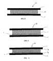
- FIGS. 4-9A variety of device constructions comprising a layer stack between a pair of vertically spaced apart first and second electrodes are possible according to the invention, as illustrated in simplified, schematic cross-sectional view in FIGS. 4-9, wherein each of the various constituent layers is comprised of one or more of the above-described materials indicated as suitable for use as that constituent layer.
- FIG. 4shows a memory device 20 according to the invention, comprising a single layer sandwiched between a pair of electrodes, i.e., a combined active layer/passive layer 3 / 5 (such as of Li x VSe 2 or Li x HfSe 2 , as described above), or a composite material comprised of a porous dielectric doped with ions or ion clusters) sandwiched between upper and lower electrodes 1 and 2 ;
- a combined active layer/passive layer 3 / 5such as of Li x VSe 2 or Li x HfSe 2 , as described above
- a composite material comprised of a porous dielectric doped with ions or ion clusterssandwiched between upper and lower electrodes 1 and 2 ;
- FIG. 5shows a memory device 30 according to the invention, comprising a layer stack sandwiched between upper and lower electrodes 1 and 2 , the layer stack including an upper, active layer 3 and a lower, passive layer 5 ;
- FIG. 6shows a memory device 40 according to the invention, comprising a layer stack sandwiched between upper and lower electrodes 1 and 2 , the layer stack including a pair of active layers 3 including a first, upper active layer 3 A and a second, lower active layer 3 B , and a lower, passive layer 5 ;
- FIG. 7shows a memory device 50 according to the invention, comprising a layer stack sandwiched between upper and lower electrodes 1 and 2 , the layer stack including an upper, active layer 3 and a lower, passive layer 5 , with a barrier layer 4 inserted between the upper, active layer 3 and the lower, passive layer 5 ;
- FIG. 8shows a memory device 60 according to the invention, comprising a layer stack sandwiched between upper and lower electrodes 1 and 2 , the layer stack including a pair of active layers 3 including a first, upper active layer 3 A and a second, lower active layer 3 B , a barrier layer 4 inserted between the first, upper active layer 3 A and the second, lower active layer 3 B , and a lower passive layer 5 ; and
- FIG. 9shows a memory device 70 according to the invention, comprising a layer stack sandwiched between upper and lower electrodes 1 and 2 , the layer stack including a first, upper passive layer 5 A , a pair of active layers 3 including a first, upper active layer 3 A and a second, lower active layer 3 B , a barrier layer 4 inserted between the first, upper active layer 3 A and the second, lower active layer 3 B , and a second, lower passive layer 5 B .
- each of the constituent layers of each of the embodiments illustrated in FIGS. 4-9are as follows:
- first and second electrically conductive electrodes 1 and 2from about 3,000 to about 8,000 ⁇ , with 5,000 ⁇ presently preferred;
- active layer 3 or active layers 3 A and 3 Bfrom about 50 to about 1,000 ⁇ thick, with 100 ⁇ presently preferred;
- passive layer 5 or passive layers 5 A and 5 Bfrom about 20 to about 100 ⁇ thick, with 50 ⁇ presently preferred;
- barrier layer 4from about 20 to about 300 ⁇ thick, with 50 ⁇ presently preferred.
- the electrodesare formed via conventional thin film deposition techniques, e.g., thermal evaporation, sputtering, e-beam evaporation, etc.;
- the passive layermay be formed by conventional thin film deposition techniques such as thermal evaporation, CVD, spin coating, or by first depositing a layer of a metal ultimately included in the passive layer, e.g., by reacting an initially formed Cu layer with a S, Se, or Te-containing gas or liquid to form a layer of a reaction product, e.g., Cu 2 S or Cu 2 Se in contact with the Cu layer;
- porous active layerssuch as porous Si or organic materials may be formed according to well-known thin film deposition techniques, such as thermal evaporation, spin coating, CVD, etc.
- Preferable pore sizesare 10-100 ⁇ , with 30 ⁇ preferred;
- active layerscomprising electrolyte clusters, i.e., groups of particles with 10-100 ⁇ sizes may be introduced into the pores of porous Si or SiO 2 in a concentration of about 10-30% by dipping the porous Si or SiO 2 in a saturated electrolyte solution, followed by evaporation of the solvent to yield particles, i.e., clusters, of electrolyte.
- HfSe 2may be prepared by CVD from HfCl 4 and H 2 Se.
- Ti/Li x VSe 2 /Al(or Ti), wherein Li x VSe 2 serves as a combined active+passive layer (as in FIG. 4 ).
- the first, or lower electrode of Ti or Alwas vapor deposited on the surface of an insulating layer at a thickness of about 3,000-8,000 ⁇ , preferably about 5,000 ⁇ .
- the Li x VSe 2 combined active+passive layerwas deposited via CVD at a thickness of about 50-300 ⁇ , preferably about 100 ⁇ , with Li ions intercalated by treatment with a solution of n-butyl lithium in hexane.
- the second, or upper electrode of Ti or Alwas vapor deposited on the Li x VSe 2 layer at a thickness of about 3,000-8,000 ⁇ , preferably about 5,000 ⁇ .
- Ti/Li x TiS 2 /VSe 2 /Al(or Ti), wherein Li x TiS 2 serves as a passive layer and VSe 2 serves as an active layer (as in FIG. 5 ).
- This cellwas fabricated in similar manner as Example 1, except that the VSe 2 active layer was deposited by CVD on the surface of the Li x TiS 2 passive layer prior to deposition of the second, upper electrode.
- the thickness of the VSe 2 active layerwas about 50-300 ⁇ , preferably 100 ⁇ .
- Li x VSe 2serves as a passive layer and HfSe 2 serves as an active layer, each layer being deposited via CVD.
- Li x VSe 2serves as a passive layer
- Li 3 Nserves as a barrier layer
- VSe 2serves as an active layer (as in FIG. 7 ).
- the Li 3 N barrier layermay also be deposited via CVD and is about 20-100 ⁇ thick, preferably about 50 ⁇ thick.
- Ti/Li x TiS 2 /a-Si/Al(or Ti), similar to Example 2, except for an amorphous silicon (a-Si) active layer (formed by CVD) substituted for VSe 2 .
- a-Siamorphous silicon
- Ti/Li x TiS 2 /p-Si/Al(or Ti), similar to Example 5, except for a porous silicon (p-Si) active layer (formed by CVD) substituted for a-Si.
- p-Siporous silicon
- Ti/Li x TiS 2 /p-SiO 2 /Al(or Ti), similar to Examples 5 and 6, except for a porous silicon dioxide (p-SiO 2 ) active layer (formed by CVD or from a sol-gel of tetraethoxyorthosilicate, TEOS) substituted for a-Si or p-Si.
- p-SiO 2porous silicon dioxide
- Ti/Cu 2 ⁇ x S/p-SiO 2 /Al(or Ti), similar to Example 7, except that Cu 2 ⁇ x S (preferably Cu 1.8 S) is substituted for Li x TiS 2 as a passive layer.
- the Cu 2 ⁇ x S passive layermay be formed by first depositing (e.g., vapor depositing) an about 100-300 ⁇ thick layer of Cu (150 ⁇ presently preferred) on the surface of the lower electrode (Ti), followed by an about 15 min. treatment of the Cu layer with H 2 S gas in a chamber at room temperature for reaction to form Cu 2 ⁇ x S.
- Ti/Cu 2 ⁇ x S/Cu 2 O/Alsimilar to Example 8, except that CuO is substituted for p-SiO 2 as an active layer.
- the Cu 2 ⁇ x S passive layeris first formed by depositing (e.g., vapor depositing) an about 200-400 ⁇ thick layer of Cu (250 ⁇ presently preferred) on the surface of the lower electrode (Ti), followed by an about 10 min. treatment of the Cu layer with H 2 S gas in a chamber at room temperature for reaction to form Cu 2 ⁇ x S.
- the Cu 2 ⁇ x S layeris then reacted with O 2 gas in a chamber for about 10 min. to form a layer of Cu 2 O over the layer of Cu 2 ⁇ x S.
- Ti/Cu 2 ⁇ x Se/p-SiO 2 /Al(or Ti), similar to Example 8, except that Cu 2 ⁇ x Se is substituted for Cu 2 ⁇ x S as the passive layer by using H 2 Se gas in place of H 2 S for reaction with the initially deposited Cu layer.
- the Ag 2 S passive layermay be formed by first depositing (e.g., vapor depositing) an about 100-300 ⁇ thick layer of Ag (150 ⁇ presently preferred) on the surface of the lower electrode (Ti), followed by about 15 min. reaction with H 2 S in a chamber at room temperature to form Ag 2 S.
- Ti/Cu 2 ⁇ x S/BN/Alsimilar to Example 8, with an about 50-300 ⁇ thick layer of CVD-deposited BN (100 ⁇ presently preferred) substituted for p-SiO 2 as the active layer.
- Ti/Cu 2 ⁇ x S/C 3 N/Alsimilar to Example 8, with an about 50-300 ⁇ thick layer of CVD-deposited, amorphous C 3 N (100 ⁇ presently preferred) substituted for p-SiO 2 as the active layer.
- Ti/Cu 2 ⁇ x S/BaTiO 3 /Alsimilar to Example 8, with an about 50-300 ⁇ thick layer of CVD-deposited, ferroelectric BaTiO 3 (100 ⁇ presently preferred) substituted for p-SiO 2 as the active layer.
- Ti/Cu 2 ⁇ x S/polyester/Alsimilar to Example 8, with an about 50-300 ⁇ thick layer of spin-coated polystyrene (100 ⁇ presently preferred) substituted for p-SiO 2 as the active layer.
- the CuWO 3 passive layermay be formed by first depositing (e.g., vapor depositing) an about 100-300 ⁇ thick layer (150 ⁇ presently preferred) of tungsten (W) on the surface of the lower (Ti) electrode, and reacting the W layer with O 2 gas in a chamber for about 10 min. to form a layer of WO 3 .
- a layer of CuIis then spin-coated onto the layer of WO 3 and the combination reacted at about 150° C. to form Cu x WO 3 .
- the Cu—CuI passive layermay be formed by first depositing (e.g., vapor depositing) an about 100-300 ⁇ thick layer (150 ⁇ presently preferred) of copper (Cu) on the surface of the lower (Ti) electrode, followed by spin-coating a layer of CuI on the Cu layer.
- Example 11Ag/Ag 2 S/p-SiO 2 /Al (or Ti), similar to Example 11, except that the first electrode is made of Ag rather than Ti.
- inventive devices or cells fabricated according to the inventive concept and methodologyreflect the extreme flexibility and versatility with regard to device structures and materials selection afforded by the present invention.
- the inventive devicesare well suited for use in a variety of applications currently employing conventional semiconductor-based memory devices.
- the inventive memory devicesare readily fabricated in cost-effective manner utilizing conventional manufacturing technologies.
Landscapes
- Engineering & Computer Science (AREA)
- Chemical & Material Sciences (AREA)
- Computer Hardware Design (AREA)
- Nanotechnology (AREA)
- Crystallography & Structural Chemistry (AREA)
- Theoretical Computer Science (AREA)
- Mathematical Physics (AREA)
- Physics & Mathematics (AREA)
- Manufacturing & Machinery (AREA)
- Materials Engineering (AREA)
- Semiconductor Memories (AREA)
- Nitrogen And Oxygen Or Sulfur-Condensed Heterocyclic Ring Systems (AREA)
- Read Only Memory (AREA)
Abstract
Description
Claims (30)
Priority Applications (5)
| Application Number | Priority Date | Filing Date | Title |
|---|---|---|---|
| US10/304,863US6806526B2 (en) | 2001-08-13 | 2002-11-27 | Memory device |
| US10/414,353US6864522B2 (en) | 2001-08-13 | 2003-04-15 | Memory device |
| US10/413,829US6768157B2 (en) | 2001-08-13 | 2003-04-15 | Memory device |
| US10/413,818US6858481B2 (en) | 2001-08-13 | 2003-04-15 | Memory device with active and passive layers |
| US10/413,841US6838720B2 (en) | 2001-08-13 | 2003-04-15 | Memory device with active passive layers |
Applications Claiming Priority (1)
| Application Number | Priority Date | Filing Date | Title |
|---|---|---|---|
| PCT/RU2001/000334WO2003017282A1 (en) | 2001-08-13 | 2001-08-13 | Memory cell |
Related Parent Applications (2)
| Application Number | Title | Priority Date | Filing Date |
|---|---|---|---|
| PCT/RU2001/000334Continuation-In-PartWO2003017282A1 (en) | 2001-08-13 | 2001-08-13 | Memory cell |
| US10/304,863Continuation-In-PartUS6806526B2 (en) | 2001-08-13 | 2002-11-27 | Memory device |
Related Child Applications (6)
| Application Number | Title | Priority Date | Filing Date |
|---|---|---|---|
| PCT/RU2001/000334Continuation-In-PartWO2003017282A1 (en) | 2001-08-13 | 2001-08-13 | Memory cell |
| US10/304,863Continuation-In-PartUS6806526B2 (en) | 2001-08-13 | 2002-11-27 | Memory device |
| US10/413,818Continuation-In-PartUS6858481B2 (en) | 2001-08-13 | 2003-04-15 | Memory device with active and passive layers |
| US10/414,353ContinuationUS6864522B2 (en) | 2001-08-13 | 2003-04-15 | Memory device |
| US10/413,841Continuation-In-PartUS6838720B2 (en) | 2001-08-13 | 2003-04-15 | Memory device with active passive layers |
| US10/413,829Continuation-In-PartUS6768157B2 (en) | 2001-08-13 | 2003-04-15 | Memory device |
Publications (2)
| Publication Number | Publication Date |
|---|---|
| US20030053350A1 US20030053350A1 (en) | 2003-03-20 |
| US6815286B2true US6815286B2 (en) | 2004-11-09 |
Family
ID=20129643
Family Applications (5)
| Application Number | Title | Priority Date | Filing Date |
|---|---|---|---|
| US10/486,864Expired - LifetimeUS6992323B2 (en) | 2001-08-13 | 2001-08-13 | Memory cell |
| US10/238,880Expired - LifetimeUS6815286B2 (en) | 2001-08-13 | 2002-09-11 | Memory device |
| US10/414,353Expired - LifetimeUS6864522B2 (en) | 2001-08-13 | 2003-04-15 | Memory device |
| US10/776,850Expired - Fee RelatedUS7026702B2 (en) | 2001-08-13 | 2004-02-11 | Memory device |
| US10/776,870Expired - Fee RelatedUS7254053B2 (en) | 2001-08-13 | 2004-02-11 | Active programming and operation of a memory device |
Family Applications Before (1)
| Application Number | Title | Priority Date | Filing Date |
|---|---|---|---|
| US10/486,864Expired - LifetimeUS6992323B2 (en) | 2001-08-13 | 2001-08-13 | Memory cell |
Family Applications After (3)
| Application Number | Title | Priority Date | Filing Date |
|---|---|---|---|
| US10/414,353Expired - LifetimeUS6864522B2 (en) | 2001-08-13 | 2003-04-15 | Memory device |
| US10/776,850Expired - Fee RelatedUS7026702B2 (en) | 2001-08-13 | 2004-02-11 | Memory device |
| US10/776,870Expired - Fee RelatedUS7254053B2 (en) | 2001-08-13 | 2004-02-11 | Active programming and operation of a memory device |
Country Status (8)
| Country | Link |
|---|---|
| US (5) | US6992323B2 (en) |
| EP (1) | EP1434232B1 (en) |
| JP (1) | JP2005500682A (en) |
| KR (1) | KR100860134B1 (en) |
| CN (1) | CN100419906C (en) |
| BR (1) | BR0117103A (en) |
| DE (1) | DE60130586T2 (en) |
| WO (1) | WO2003017282A1 (en) |
Cited By (71)
| Publication number | Priority date | Publication date | Assignee | Title |
|---|---|---|---|---|
| US20040245517A1 (en)* | 2003-06-03 | 2004-12-09 | Campbell Kristy A. | Diode/superionic conductor/polymer memory structure |
| US20050277234A1 (en)* | 2003-04-15 | 2005-12-15 | Erik Brandon | Flexible carbon-based ohmic contacts for organic transistors |
| US7102156B1 (en)* | 2004-12-23 | 2006-09-05 | Spansion Llc Advanced Micro Devices, Inc | Memory elements using organic active layer |
| US20070008603A1 (en)* | 2005-07-11 | 2007-01-11 | Sotzing Gregory A | Electrochromic devices utilizing very low band gap conjugated counter electrodes: preparation and use |
| US20070230235A1 (en)* | 2004-11-26 | 2007-10-04 | C/O Semiconductor Energy Laboratory Co., Ltd. | Semiconductor Device |
| US7307321B1 (en)* | 2005-03-25 | 2007-12-11 | Spansion Llc | Memory device with improved data retention |
| US20080001143A1 (en)* | 2006-06-28 | 2008-01-03 | Semiconductor Energy Laboratory Co., Ltd. | Semiconductor device and manufacturing method thereof |
| US20080017849A1 (en)* | 2006-03-10 | 2008-01-24 | Semiconductor Energy Laboratory Co., Ltd. | Memory element and semiconductor device |
| US20090014707A1 (en)* | 2006-10-20 | 2009-01-15 | Wei Lu | Non-volatile solid state resistive switching devices |
| US20090140231A1 (en)* | 2005-04-27 | 2009-06-04 | Semiconductor Energy Labortory Co., Ltd. | Semiconductor device and method of manufacturing the same |
| US20110120856A1 (en)* | 2009-11-23 | 2011-05-26 | International Business Machines Corporation | Memory Cell and Select Element |
| US8374018B2 (en) | 2010-07-09 | 2013-02-12 | Crossbar, Inc. | Resistive memory using SiGe material |
| US8391049B2 (en) | 2010-09-29 | 2013-03-05 | Crossbar, Inc. | Resistor structure for a non-volatile memory device and method |
| US8394670B2 (en) | 2011-05-31 | 2013-03-12 | Crossbar, Inc. | Vertical diodes for non-volatile memory device |
| US8399881B2 (en) | 2005-03-25 | 2013-03-19 | Semiconductor Energy Laboratory Co., Ltd. | Memory element, memory device, and semiconductor device |
| US8404553B2 (en) | 2010-08-23 | 2013-03-26 | Crossbar, Inc. | Disturb-resistant non-volatile memory device and method |
| US8441835B2 (en) | 2010-06-11 | 2013-05-14 | Crossbar, Inc. | Interface control for improved switching in RRAM |
| US8450710B2 (en) | 2011-05-27 | 2013-05-28 | Crossbar, Inc. | Low temperature p+ silicon junction material for a non-volatile memory device |
| US8450209B2 (en) | 2010-11-05 | 2013-05-28 | Crossbar, Inc. | p+ Polysilicon material on aluminum for non-volatile memory device and method |
| US8467227B1 (en) | 2010-11-04 | 2013-06-18 | Crossbar, Inc. | Hetero resistive switching material layer in RRAM device and method |
| US8492195B2 (en) | 2010-08-23 | 2013-07-23 | Crossbar, Inc. | Method for forming stackable non-volatile resistive switching memory devices |
| US8519485B2 (en) | 2010-06-11 | 2013-08-27 | Crossbar, Inc. | Pillar structure for memory device and method |
| US8558212B2 (en) | 2010-09-29 | 2013-10-15 | Crossbar, Inc. | Conductive path in switching material in a resistive random access memory device and control |
| US8658476B1 (en) | 2012-04-20 | 2014-02-25 | Crossbar, Inc. | Low temperature P+ polycrystalline silicon material for non-volatile memory device |
| US8659929B2 (en) | 2011-06-30 | 2014-02-25 | Crossbar, Inc. | Amorphous silicon RRAM with non-linear device and operation |
| US8716098B1 (en) | 2012-03-09 | 2014-05-06 | Crossbar, Inc. | Selective removal method and structure of silver in resistive switching device for a non-volatile memory device |
| US8765566B2 (en) | 2012-05-10 | 2014-07-01 | Crossbar, Inc. | Line and space architecture for a non-volatile memory device |
| US8790819B1 (en)* | 2006-10-06 | 2014-07-29 | Greatbatch Ltd. | Implantable medical assembly |
| US8791010B1 (en) | 2010-12-31 | 2014-07-29 | Crossbar, Inc. | Silver interconnects for stacked non-volatile memory device and method |
| US8796658B1 (en) | 2012-05-07 | 2014-08-05 | Crossbar, Inc. | Filamentary based non-volatile resistive memory device and method |
| US8809831B2 (en) | 2010-07-13 | 2014-08-19 | Crossbar, Inc. | On/off ratio for non-volatile memory device and method |
| US8815696B1 (en) | 2010-12-31 | 2014-08-26 | Crossbar, Inc. | Disturb-resistant non-volatile memory device using via-fill and etchback technique |
| US8884261B2 (en) | 2010-08-23 | 2014-11-11 | Crossbar, Inc. | Device switching using layered device structure |
| US8889521B1 (en) | 2012-09-14 | 2014-11-18 | Crossbar, Inc. | Method for silver deposition for a non-volatile memory device |
| US8930174B2 (en) | 2010-12-28 | 2015-01-06 | Crossbar, Inc. | Modeling technique for resistive random access memory (RRAM) cells |
| US8934280B1 (en) | 2013-02-06 | 2015-01-13 | Crossbar, Inc. | Capacitive discharge programming for two-terminal memory cells |
| US8947908B2 (en) | 2010-11-04 | 2015-02-03 | Crossbar, Inc. | Hetero-switching layer in a RRAM device and method |
| US8946673B1 (en) | 2012-08-24 | 2015-02-03 | Crossbar, Inc. | Resistive switching device structure with improved data retention for non-volatile memory device and method |
| US8946669B1 (en) | 2012-04-05 | 2015-02-03 | Crossbar, Inc. | Resistive memory device and fabrication methods |
| US8946046B1 (en) | 2012-05-02 | 2015-02-03 | Crossbar, Inc. | Guided path for forming a conductive filament in RRAM |
| US8982647B2 (en) | 2012-11-14 | 2015-03-17 | Crossbar, Inc. | Resistive random access memory equalization and sensing |
| US9012307B2 (en) | 2010-07-13 | 2015-04-21 | Crossbar, Inc. | Two terminal resistive switching device structure and method of fabricating |
| US9087576B1 (en) | 2012-03-29 | 2015-07-21 | Crossbar, Inc. | Low temperature fabrication method for a three-dimensional memory device and structure |
| US9112145B1 (en) | 2013-01-31 | 2015-08-18 | Crossbar, Inc. | Rectified switching of two-terminal memory via real time filament formation |
| US9153623B1 (en) | 2010-12-31 | 2015-10-06 | Crossbar, Inc. | Thin film transistor steering element for a non-volatile memory device |
| US9191000B2 (en) | 2011-07-29 | 2015-11-17 | Crossbar, Inc. | Field programmable gate array utilizing two-terminal non-volatile memory |
| US9252191B2 (en) | 2011-07-22 | 2016-02-02 | Crossbar, Inc. | Seed layer for a p+ silicon germanium material for a non-volatile memory device and method |
| US9312483B2 (en) | 2012-09-24 | 2016-04-12 | Crossbar, Inc. | Electrode structure for a non-volatile memory device and method |
| US9324942B1 (en) | 2013-01-31 | 2016-04-26 | Crossbar, Inc. | Resistive memory cell with solid state diode |
| US9401475B1 (en) | 2010-08-23 | 2016-07-26 | Crossbar, Inc. | Method for silver deposition for a non-volatile memory device |
| US9406379B2 (en) | 2013-01-03 | 2016-08-02 | Crossbar, Inc. | Resistive random access memory with non-linear current-voltage relationship |
| US9412790B1 (en) | 2012-12-04 | 2016-08-09 | Crossbar, Inc. | Scalable RRAM device architecture for a non-volatile memory device and method |
| US9520557B2 (en) | 2008-10-20 | 2016-12-13 | The Regents Of The University Of Michigan | Silicon based nanoscale crossbar memory |
| US9543359B2 (en) | 2011-05-31 | 2017-01-10 | Crossbar, Inc. | Switching device having a non-linear element |
| US9564587B1 (en) | 2011-06-30 | 2017-02-07 | Crossbar, Inc. | Three-dimensional two-terminal memory with enhanced electric field and segmented interconnects |
| US9570678B1 (en) | 2010-06-08 | 2017-02-14 | Crossbar, Inc. | Resistive RAM with preferental filament formation region and methods |
| US9576616B2 (en) | 2012-10-10 | 2017-02-21 | Crossbar, Inc. | Non-volatile memory with overwrite capability and low write amplification |
| US9583701B1 (en) | 2012-08-14 | 2017-02-28 | Crossbar, Inc. | Methods for fabricating resistive memory device switching material using ion implantation |
| USRE46335E1 (en) | 2010-11-04 | 2017-03-07 | Crossbar, Inc. | Switching device having a non-linear element |
| US9601690B1 (en) | 2011-06-30 | 2017-03-21 | Crossbar, Inc. | Sub-oxide interface layer for two-terminal memory |
| US9601692B1 (en) | 2010-07-13 | 2017-03-21 | Crossbar, Inc. | Hetero-switching layer in a RRAM device and method |
| US9620206B2 (en) | 2011-05-31 | 2017-04-11 | Crossbar, Inc. | Memory array architecture with two-terminal memory cells |
| US9627443B2 (en) | 2011-06-30 | 2017-04-18 | Crossbar, Inc. | Three-dimensional oblique two-terminal memory with enhanced electric field |
| US9633723B2 (en) | 2011-06-23 | 2017-04-25 | Crossbar, Inc. | High operating speed resistive random access memory |
| US9685608B2 (en) | 2012-04-13 | 2017-06-20 | Crossbar, Inc. | Reduced diffusion in metal electrode for two-terminal memory |
| US9729155B2 (en) | 2011-07-29 | 2017-08-08 | Crossbar, Inc. | Field programmable gate array utilizing two-terminal non-volatile memory |
| US9735358B2 (en) | 2012-08-14 | 2017-08-15 | Crossbar, Inc. | Noble metal / non-noble metal electrode for RRAM applications |
| US9741765B1 (en) | 2012-08-14 | 2017-08-22 | Crossbar, Inc. | Monolithically integrated resistive memory using integrated-circuit foundry compatible processes |
| US10056907B1 (en) | 2011-07-29 | 2018-08-21 | Crossbar, Inc. | Field programmable gate array utilizing two-terminal non-volatile memory |
| US10290801B2 (en) | 2014-02-07 | 2019-05-14 | Crossbar, Inc. | Scalable silicon based resistive memory device |
| US11068620B2 (en) | 2012-11-09 | 2021-07-20 | Crossbar, Inc. | Secure circuit integrated with memory layer |
Families Citing this family (196)
| Publication number | Priority date | Publication date | Assignee | Title |
|---|---|---|---|---|
| WO2002091496A2 (en) | 2001-05-07 | 2002-11-14 | Advanced Micro Devices, Inc. | Reversible field-programmable electric interconnects |
| KR100900080B1 (en) | 2001-05-07 | 2009-06-01 | 어드밴스드 마이크로 디바이시즈, 인코포레이티드 | Memory device having self-assembled polymer film and manufacturing method thereof |
| US6873540B2 (en) | 2001-05-07 | 2005-03-29 | Advanced Micro Devices, Inc. | Molecular memory cell |
| WO2002091495A2 (en) | 2001-05-07 | 2002-11-14 | Coatue Corporation | Molecular memory device |
| CN100367528C (en) | 2001-05-07 | 2008-02-06 | 先进微装置公司 | Switching device with memory effect |
| US6768157B2 (en) | 2001-08-13 | 2004-07-27 | Advanced Micro Devices, Inc. | Memory device |
| US6806526B2 (en) | 2001-08-13 | 2004-10-19 | Advanced Micro Devices, Inc. | Memory device |
| US6838720B2 (en) | 2001-08-13 | 2005-01-04 | Advanced Micro Devices, Inc. | Memory device with active passive layers |
| WO2003017282A1 (en) | 2001-08-13 | 2003-02-27 | Advanced Micro Devices, Inc. | Memory cell |
| US6858481B2 (en) | 2001-08-13 | 2005-02-22 | Advanced Micro Devices, Inc. | Memory device with active and passive layers |
| US9269043B2 (en) | 2002-03-12 | 2016-02-23 | Knowm Tech, Llc | Memristive neural processor utilizing anti-hebbian and hebbian technology |
| US7392230B2 (en) | 2002-03-12 | 2008-06-24 | Knowmtech, Llc | Physical neural network liquid state machine utilizing nanotechnology |
| US8156057B2 (en) | 2003-03-27 | 2012-04-10 | Knowm Tech, Llc | Adaptive neural network utilizing nanotechnology-based components |
| US6889216B2 (en) | 2002-03-12 | 2005-05-03 | Knowm Tech, Llc | Physical neural network design incorporating nanotechnology |
| US7398259B2 (en) | 2002-03-12 | 2008-07-08 | Knowmtech, Llc | Training of a physical neural network |
| US7412428B2 (en) | 2002-03-12 | 2008-08-12 | Knowmtech, Llc. | Application of hebbian and anti-hebbian learning to nanotechnology-based physical neural networks |
| US7752151B2 (en) | 2002-06-05 | 2010-07-06 | Knowmtech, Llc | Multilayer training in a physical neural network formed utilizing nanotechnology |
| US7827131B2 (en) | 2002-08-22 | 2010-11-02 | Knowm Tech, Llc | High density synapse chip using nanoparticles |
| US7012276B2 (en) | 2002-09-17 | 2006-03-14 | Advanced Micro Devices, Inc. | Organic thin film Zener diodes |
| US6836398B1 (en)* | 2002-10-31 | 2004-12-28 | Advanced Micro Devices, Inc. | System and method of forming a passive layer by a CMP process |
| WO2004070789A2 (en)* | 2003-02-03 | 2004-08-19 | The Regent Of The University Of California | Rewritable nano-surface organic electrical bistable devices |
| US6656763B1 (en)* | 2003-03-10 | 2003-12-02 | Advanced Micro Devices, Inc. | Spin on polymers for organic memory devices |
| US6995445B2 (en)* | 2003-03-14 | 2006-02-07 | The Trustees Of Princeton University | Thin film organic position sensitive detectors |
| US6977389B2 (en)* | 2003-06-02 | 2005-12-20 | Advanced Micro Devices, Inc. | Planar polymer memory device |
| US20050006640A1 (en)* | 2003-06-26 | 2005-01-13 | Jackson Warren B. | Polymer-based memory element |
| US6787458B1 (en)* | 2003-07-07 | 2004-09-07 | Advanced Micro Devices, Inc. | Polymer memory device formed in via opening |
| US7259039B2 (en)* | 2003-07-09 | 2007-08-21 | Spansion Llc | Memory device and methods of using and making the device |
| JP4321524B2 (en)* | 2003-07-18 | 2009-08-26 | 日本電気株式会社 | Switching element, switching element driving method, rewritable logic integrated circuit, and memory element |
| US7426501B2 (en) | 2003-07-18 | 2008-09-16 | Knowntech, Llc | Nanotechnology neural network methods and systems |
| KR100615586B1 (en)* | 2003-07-23 | 2006-08-25 | 삼성전자주식회사 | Phase change memory device having a local phase change region in a porous dielectric film and a method of manufacturing the same |
| US7274035B2 (en)* | 2003-09-03 | 2007-09-25 | The Regents Of The University Of California | Memory devices based on electric field programmable films |
| DE10342026A1 (en)* | 2003-09-11 | 2005-04-28 | Infineon Technologies Ag | Memory cell with ion conduction storage mechanism and method for its production |
| US6852586B1 (en)* | 2003-10-01 | 2005-02-08 | Advanced Micro Devices, Inc. | Self assembly of conducting polymer for formation of polymer memory cell |
| US7015504B2 (en)* | 2003-11-03 | 2006-03-21 | Advanced Micro Devices, Inc. | Sidewall formation for high density polymer memory element array |
| JP2005150156A (en)* | 2003-11-11 | 2005-06-09 | Toshiba Corp | Magnetic storage |
| WO2005086627A2 (en)* | 2003-12-03 | 2005-09-22 | The Regents Of The University Of California | Three-terminal electrical bistable devices |
| JP4385778B2 (en)* | 2004-01-29 | 2009-12-16 | ソニー株式会社 | Storage device |
| US6956761B2 (en)* | 2004-03-10 | 2005-10-18 | Micron Technology, Inc. | Method to manufacture polymer memory with copper ion switching species |
| CA2500938A1 (en)* | 2004-03-24 | 2005-09-24 | Rohm And Haas Company | Memory devices based on electric field programmable films |
| ATE486369T1 (en)* | 2004-03-26 | 2010-11-15 | Nxp Bv | ELECTRICAL DEVICE COMPRISING A PHASE CHANGE MATERIAL |
| US7205595B2 (en)* | 2004-03-31 | 2007-04-17 | Intel Corporation | Polymer memory device with electron traps |
| US7608855B2 (en)* | 2004-04-02 | 2009-10-27 | Spansion Llc | Polymer dielectrics for memory element array interconnect |
| WO2006001923A2 (en)* | 2004-05-17 | 2006-01-05 | The Regents Of The University Of California | Bistable nanoparticle- polymer composite for use in memory devices |
| US20050274609A1 (en)* | 2004-05-18 | 2005-12-15 | Yong Chen | Composition of matter which results in electronic switching through intra- or inter- molecular charge transfer, or charge transfer between molecules and electrodes induced by an electrical field |
| DE102004024610B3 (en)* | 2004-05-18 | 2005-12-29 | Infineon Technologies Ag | Solid electrolyte switching element |
| US7554111B2 (en)* | 2004-05-20 | 2009-06-30 | The Regents Of The University Of California | Nanoparticle-polymer bistable devices |
| DE102004031135A1 (en)* | 2004-06-28 | 2006-01-19 | Infineon Technologies Ag | Resistive semiconductor element based on a solid-state ion conductor |
| US7157732B2 (en)* | 2004-07-01 | 2007-01-02 | Spansion Llc | Switchable memory diode-a new memory device |
| US7220982B2 (en)* | 2004-07-27 | 2007-05-22 | Micron Technology, Inc. | Amorphous carbon-based non-volatile memory |
| US20060035474A1 (en)* | 2004-08-10 | 2006-02-16 | Pavel Komilovich | Increasing retention time for memory devices |
| US7199394B2 (en)* | 2004-08-17 | 2007-04-03 | Spansion Llc | Polymer memory device with variable period of retention time |
| US7289353B2 (en) | 2004-08-17 | 2007-10-30 | Spansion, Llc | Systems and methods for adjusting programming thresholds of polymer memory cells |
| US7166543B2 (en)* | 2004-08-30 | 2007-01-23 | Micron Technology, Inc. | Methods for forming an enriched metal oxide surface for use in a semiconductor device |
| DE102004046392A1 (en)* | 2004-09-24 | 2006-04-06 | Infineon Technologies Ag | Semiconductor memory |
| WO2006039439A2 (en) | 2004-09-30 | 2006-04-13 | Cummins-Allison Corp. | Magnetic detection system for use in currency processing and method and apparatus for using the same |
| US7557782B2 (en)* | 2004-10-20 | 2009-07-07 | Hewlett-Packard Development Company, L.P. | Display device including variable optical element and programmable resistance element |
| GB2437188A (en)* | 2004-10-28 | 2007-10-17 | Univ California | Organic-complex thin film for nonvolatile memory applications |
| US7221599B1 (en)* | 2004-11-01 | 2007-05-22 | Spansion, Llc | Polymer memory cell operation |
| US7876596B2 (en)* | 2004-11-08 | 2011-01-25 | Waseda University | Memory element and method for manufacturing same |
| KR100657911B1 (en)* | 2004-11-10 | 2006-12-14 | 삼성전자주식회사 | Nonvolatile Memory Device with One Resistor and One Diode |
| KR100651656B1 (en)* | 2004-11-29 | 2006-12-01 | 한국과학기술연구원 | Phase Change Memory Cells with Transparent Conductive Oxide Electrode Contact Materials |
| EP1820215A4 (en)* | 2004-12-07 | 2008-11-12 | Semiconductor Energy Lab | MEMORY DEVICE AND SEMICONDUCTOR DEVICE |
| FR2880177B1 (en) | 2004-12-23 | 2007-05-18 | Commissariat Energie Atomique | MEMORY PMC HAVING IMPROVED RETENTION TIME AND WRITING SPEED |
| US7208757B1 (en)* | 2004-12-23 | 2007-04-24 | Spansion Llc | Memory element with nitrogen-containing active layer |
| US7273766B1 (en)* | 2005-01-12 | 2007-09-25 | Spansion Llc | Variable density and variable persistent organic memory devices, methods, and fabrication |
| US7084062B1 (en) | 2005-01-12 | 2006-08-01 | Advanced Micro Devices, Inc. | Use of Ta-capped metal line to improve formation of memory element films |
| KR101067582B1 (en)* | 2005-01-20 | 2011-09-27 | 삼성전자주식회사 | Multi-State Driving Method of Memory Devices |
| DE102005004107A1 (en)* | 2005-01-28 | 2006-08-17 | Infineon Technologies Ag | Integrated semiconductor memory with an arrangement of nonvolatile memory cells and method |
| US7502769B2 (en) | 2005-01-31 | 2009-03-10 | Knowmtech, Llc | Fractal memory and computational methods and systems based on nanotechnology |
| KR101078125B1 (en)* | 2005-02-07 | 2011-10-28 | 삼성전자주식회사 | Nonvolatile Nano-channel Memory Device using Mesoporous Material |
| KR101036975B1 (en)* | 2005-02-14 | 2011-05-25 | 삼성전자주식회사 | Resistive memory devices with resistor part for controlling switching window |
| US8193606B2 (en) | 2005-02-28 | 2012-06-05 | Semiconductor Energy Laboratory Co., Ltd. | Semiconductor device including a memory element |
| KR100682939B1 (en) | 2005-03-16 | 2007-02-15 | 삼성전자주식회사 | Semiconductor memory device using solid electrolyte of three-dimensional structure and manufacturing method thereof |
| US7145824B2 (en)* | 2005-03-22 | 2006-12-05 | Spansion Llc | Temperature compensation of thin film diode voltage threshold in memory sensing circuit |
| US7579631B2 (en)* | 2005-03-22 | 2009-08-25 | Spansion Llc | Variable breakdown characteristic diode |
| US7180770B2 (en)* | 2005-03-24 | 2007-02-20 | Hewlett-Packard Development Company, L.P. | Series diode thermally assisted MRAM |
| US7830015B2 (en)* | 2005-03-25 | 2010-11-09 | Spansion Llc | Memory device with improved data retention |
| US8098521B2 (en)* | 2005-03-31 | 2012-01-17 | Spansion Llc | Method of providing an erase activation energy of a memory device |
| US7344913B1 (en) | 2005-04-06 | 2008-03-18 | Spansion Llc | Spin on memory cell active layer doped with metal ions |
| US7776682B1 (en)* | 2005-04-20 | 2010-08-17 | Spansion Llc | Ordered porosity to direct memory element formation |
| US20060245235A1 (en)* | 2005-05-02 | 2006-11-02 | Advanced Micro Devices, Inc. | Design and operation of a resistance switching memory cell with diode |
| US7812404B2 (en)* | 2005-05-09 | 2010-10-12 | Sandisk 3D Llc | Nonvolatile memory cell comprising a diode and a resistance-switching material |
| US20060256608A1 (en)* | 2005-05-11 | 2006-11-16 | Spansion Llc | Resistive memory device with improved data retention and reduced power |
| JP4552752B2 (en)* | 2005-05-16 | 2010-09-29 | ソニー株式会社 | Storage element manufacturing method and storage device manufacturing method |
| NO324539B1 (en)* | 2005-06-14 | 2007-11-19 | Thin Film Electronics Asa | Process in the manufacture of a ferroelectric memory device |
| US7286388B1 (en)* | 2005-06-23 | 2007-10-23 | Spansion Llc | Resistive memory device with improved data retention |
| US7361586B2 (en)* | 2005-07-01 | 2008-04-22 | Spansion Llc | Preamorphization to minimize void formation |
| US20070009821A1 (en)* | 2005-07-08 | 2007-01-11 | Charlotte Cutler | Devices containing multi-bit data |
| US7935957B2 (en)* | 2005-08-12 | 2011-05-03 | Semiconductor Energy Laboratory Co., Ltd. | Memory device and a semiconductor device |
| RU2297625C1 (en)* | 2005-09-14 | 2007-04-20 | Сергей Анатольевич Ермаков | Electrolytic memory cell for electronic memorizing devices and method for manufacturing said devices |
| US7582893B2 (en)* | 2005-09-15 | 2009-09-01 | Spansion Llc | Semiconductor memory device comprising one or more injecting bilayer electrodes |
| US7633129B1 (en)* | 2005-09-16 | 2009-12-15 | Spansion Llc | Memory devices with active and passive layers having multiple self-assembled sublayers |
| US7307280B1 (en)* | 2005-09-16 | 2007-12-11 | Spansion Llc | Memory devices with active and passive doped sol-gel layers |
| US7268364B2 (en)* | 2005-09-23 | 2007-09-11 | Aculon, Inc. | Hybrid devices |
| US7632706B2 (en)* | 2005-10-21 | 2009-12-15 | Spansion Llc | System and method for processing an organic memory cell |
| US7741638B2 (en)* | 2005-11-23 | 2010-06-22 | Hewlett-Packard Development Company, L.P. | Control layer for a nanoscale electronic switching device |
| US8173995B2 (en)* | 2005-12-23 | 2012-05-08 | E. I. Du Pont De Nemours And Company | Electronic device including an organic active layer and process for forming the electronic device |
| FR2895531B1 (en)* | 2005-12-23 | 2008-05-09 | Commissariat Energie Atomique | IMPROVED METHOD FOR MAKING MEMORY CELLS OF THE PMC TYPE |
| KR20070075812A (en)* | 2006-01-16 | 2007-07-24 | 삼성전자주식회사 | Resistive memory device including an amorphous solid electrolyte layer in a storage node |
| KR101206605B1 (en)* | 2006-02-02 | 2012-11-29 | 삼성전자주식회사 | Organic memory devices and preparation method thereof |
| JP5417709B2 (en)* | 2006-02-09 | 2014-02-19 | 日本電気株式会社 | Switching element, rewritable logic integrated circuit, and memory element |
| US8089110B1 (en)* | 2006-02-09 | 2012-01-03 | Spansion Llc | Switchable memory diodes based on ferroelectric/conjugated polymer heterostructures and/or their composites |
| US7605410B2 (en)* | 2006-02-23 | 2009-10-20 | Semiconductor Energy Laboratory Co., Ltd. | Semiconductor device and manufacturing method thereof |
| US7875871B2 (en)* | 2006-03-31 | 2011-01-25 | Sandisk 3D Llc | Heterojunction device comprising a semiconductor and a resistivity-switching oxide or nitride |
| US8502198B2 (en)* | 2006-04-28 | 2013-08-06 | Hewlett-Packard Development Company, L.P. | Switching device and methods for controlling electron tunneling therein |
| US8115282B2 (en)* | 2006-07-25 | 2012-02-14 | Adesto Technology Corporation | Memory cell device and method of manufacture |
| EP1883109B1 (en)* | 2006-07-28 | 2013-05-15 | Semiconductor Energy Laboratory Co., Ltd. | Memory element and method of manufacturing thereof |
| FR2905028B1 (en)* | 2006-08-21 | 2008-12-19 | Commissariat Energie Atomique | ELECTROCHEMICAL MEMORY DEVICE |
| KR100836759B1 (en)* | 2006-10-04 | 2008-06-10 | 삼성전자주식회사 | Organic memory device and method of forming the same |
| KR101249117B1 (en)* | 2006-11-13 | 2013-03-29 | 삼성전자주식회사 | Metallocenyl dendrimer, organic memory device using the same and preparation method thereof |
| US7988057B2 (en) | 2006-11-28 | 2011-08-02 | Semiconductor Energy Laboratory Co., Ltd. | Memory device and semiconductor device |
| US7902086B2 (en)* | 2006-12-08 | 2011-03-08 | Spansion Llc | Prevention of oxidation of carrier ions to improve memory retention properties of polymer memory cell |
| US7449742B2 (en)* | 2006-12-20 | 2008-11-11 | Spansion Llc | Memory device with active layer of dendrimeric material |
| US7930257B2 (en) | 2007-01-05 | 2011-04-19 | Knowm Tech, Llc | Hierarchical temporal memory utilizing nanotechnology |
| KR101313784B1 (en)* | 2007-01-12 | 2013-10-01 | 삼성전자주식회사 | Resistive random access memory device and method for manufacturing the same |
| US7667220B2 (en)* | 2007-01-19 | 2010-02-23 | Macronix International Co., Ltd. | Multilevel-cell memory structures employing multi-memory with tungsten oxides and manufacturing method |
| US8373148B2 (en)* | 2007-04-26 | 2013-02-12 | Spansion Llc | Memory device with improved performance |
| US8233308B2 (en)* | 2007-06-29 | 2012-07-31 | Sandisk 3D Llc | Memory cell that employs a selectively deposited reversible resistance-switching element and methods of forming the same |
| US7824956B2 (en) | 2007-06-29 | 2010-11-02 | Sandisk 3D Llc | Memory cell that employs a selectively grown reversible resistance-switching element and methods of forming the same |
| US7902537B2 (en) | 2007-06-29 | 2011-03-08 | Sandisk 3D Llc | Memory cell that employs a selectively grown reversible resistance-switching element and methods of forming the same |
| US20090104756A1 (en)* | 2007-06-29 | 2009-04-23 | Tanmay Kumar | Method to form a rewriteable memory cell comprising a diode and a resistivity-switching grown oxide |
| JP5227544B2 (en)* | 2007-07-12 | 2013-07-03 | 株式会社日立製作所 | Semiconductor device |
| RU2376677C2 (en)* | 2007-07-23 | 2009-12-20 | Физико-технологический институт Российской академии наук (статус государственного учреждения) | Memory cell with conducting layer-dielectric-conducting layer structure |
| US8946020B2 (en)* | 2007-09-06 | 2015-02-03 | Spansion, Llc | Method of forming controllably conductive oxide |
| FR2922368A1 (en)* | 2007-10-16 | 2009-04-17 | Commissariat Energie Atomique | METHOD FOR MANUFACTURING A CBRAM MEMORY HAVING IMPROVED RELIABILITY |
| US7558101B1 (en)* | 2007-12-14 | 2009-07-07 | Spansion Llc | Scan sensing method that improves sensing margins |
| FR2928768B1 (en) | 2008-03-13 | 2010-04-09 | Commissariat Energie Atomique | NON-VOLATILE ELECTROCHEMICAL MEMORY DEVICE |
| US8133793B2 (en) | 2008-05-16 | 2012-03-13 | Sandisk 3D Llc | Carbon nano-film reversible resistance-switchable elements and methods of forming the same |
| KR101435517B1 (en)* | 2008-05-28 | 2014-08-29 | 삼성전자주식회사 | Image sensor using photodetecting molecule and driving method thereof |
| US8569730B2 (en)* | 2008-07-08 | 2013-10-29 | Sandisk 3D Llc | Carbon-based interface layer for a memory device and methods of forming the same |
| US20100032640A1 (en)* | 2008-08-07 | 2010-02-11 | Sandisk 3D Llc | Memory cell that includes a carbon-based memory element and methods of forming the same |
| US20100108976A1 (en)* | 2008-10-30 | 2010-05-06 | Sandisk 3D Llc | Electronic devices including carbon-based films, and methods of forming such devices |
| US8835892B2 (en)* | 2008-10-30 | 2014-09-16 | Sandisk 3D Llc | Electronic devices including carbon nano-tube films having boron nitride-based liners, and methods of forming the same |
| US8421050B2 (en)* | 2008-10-30 | 2013-04-16 | Sandisk 3D Llc | Electronic devices including carbon nano-tube films having carbon-based liners, and methods of forming the same |
| US8183121B2 (en) | 2009-03-31 | 2012-05-22 | Sandisk 3D Llc | Carbon-based films, and methods of forming the same, having dielectric filler material and exhibiting reduced thermal resistance |
| US8519372B2 (en) | 2009-07-30 | 2013-08-27 | Hewlett-Packard Development Company, L.P. | Electroforming-free nanoscale switching device |
| WO2011041772A2 (en)* | 2009-10-02 | 2011-04-07 | The University Of Memphis Research Foundation | Memory devices, methods of storing and reading data, smm junctions, and methods of preparing alumina substrates |
| US8551855B2 (en)* | 2009-10-23 | 2013-10-08 | Sandisk 3D Llc | Memory cell that includes a carbon-based reversible resistance switching element compatible with a steering element, and methods of forming the same |
| US8481396B2 (en)* | 2009-10-23 | 2013-07-09 | Sandisk 3D Llc | Memory cell that includes a carbon-based reversible resistance switching element compatible with a steering element, and methods of forming the same |
| US20110156012A1 (en)* | 2009-11-12 | 2011-06-30 | Sony Corporation | Double layer hardmask for organic devices |
| US8551850B2 (en)* | 2009-12-07 | 2013-10-08 | Sandisk 3D Llc | Methods of forming a reversible resistance-switching metal-insulator-metal structure |
| US20120313070A1 (en)* | 2010-01-29 | 2012-12-13 | Williams R Stanley | Controlled switching memristor |
| US8389375B2 (en)* | 2010-02-11 | 2013-03-05 | Sandisk 3D Llc | Memory cell formed using a recess and methods for forming the same |
| US8416609B2 (en) | 2010-02-15 | 2013-04-09 | Micron Technology, Inc. | Cross-point memory cells, non-volatile memory arrays, methods of reading a memory cell, methods of programming a memory cell, methods of writing to and reading from a memory cell, and computer systems |
| US8437174B2 (en) | 2010-02-15 | 2013-05-07 | Micron Technology, Inc. | Memcapacitor devices, field effect transistor devices, non-volatile memory arrays, and methods of programming |
| US8237146B2 (en)* | 2010-02-24 | 2012-08-07 | Sandisk 3D Llc | Memory cell with silicon-containing carbon switching layer and methods for forming the same |
| CN101807669A (en)* | 2010-03-29 | 2010-08-18 | 南京大学 | Organic memory |
| US8471360B2 (en) | 2010-04-14 | 2013-06-25 | Sandisk 3D Llc | Memory cell with carbon switching material having a reduced cross-sectional area and methods for forming the same |
| US8735858B2 (en) | 2010-04-30 | 2014-05-27 | Hewlett-Packard Development Company, L.P. | Ionic devices with interacting species |
| KR20130119322A (en)* | 2010-05-11 | 2013-10-31 | 예다 리서치 앤드 디벨럽먼트 캄파니 리미티드 | Solid, multi-state molecular random access memory(ram) |
| US8634224B2 (en) | 2010-08-12 | 2014-01-21 | Micron Technology, Inc. | Memory cells, non-volatile memory arrays, methods of operating memory cells, methods of writing to and reading from a memory cell, and methods of programming a memory cell |
| WO2012023992A1 (en) | 2010-08-20 | 2012-02-23 | Rhodia Operations | Films containing electrically conductive polymers |
| CN102130295A (en)* | 2010-12-17 | 2011-07-20 | 天津理工大学 | A resistive variable memory based on vanadium oxide thin film and its preparation method |
| GB2488583A (en)* | 2011-03-03 | 2012-09-05 | Nds Ltd | Preventing unauthorized access to data stored in non-volatile memories |
| US8361651B2 (en) | 2011-04-29 | 2013-01-29 | Toyota Motor Engineering & Manufacturing North America, Inc. | Active material for rechargeable battery |
| KR20130022819A (en)* | 2011-08-26 | 2013-03-07 | 한양대학교 산학협력단 | Non-volatile polymer memory devices containing buffer layer and fabrication method thereof |
| CN103208514B (en)* | 2012-01-14 | 2017-05-17 | 盛况 | Semiconductor device containing metals and preparation method of semiconductor device |
| US9653159B2 (en)* | 2012-01-18 | 2017-05-16 | Xerox Corporation | Memory device based on conductance switching in polymer/electrolyte junctions |
| US8673493B2 (en) | 2012-05-29 | 2014-03-18 | Toyota Motor Engineering & Manufacturing North America, Inc. | Indium-tin binary anodes for rechargeable magnesium-ion batteries |
| US8647770B2 (en) | 2012-05-30 | 2014-02-11 | Toyota Motor Engineering & Manufacturing North America, Inc. | Bismuth-tin binary anodes for rechargeable magnesium-ion batteries |
| US9685619B2 (en) | 2012-07-09 | 2017-06-20 | Yeda Research And Development Co. Ltd. | Logic circuits with plug and play solid-state molecular chips |
| CN103078055B (en)* | 2013-01-04 | 2015-06-03 | 华中科技大学 | Unit, device and method for simulating biological neuronal synapsis |
| US9130157B2 (en) | 2013-07-26 | 2015-09-08 | Micron Technology, Inc. | Memory cells having a number of conductive diffusion barrier materials and manufacturing methods |
| CN104518083B (en)* | 2013-09-26 | 2017-03-15 | 中国科学院宁波材料技术与工程研究所 | A kind of memory element of resistive random access memory (RRAM) and preparation method thereof |
| IL229525A0 (en) | 2013-11-20 | 2014-01-30 | Yeda Res & Dev | Metal-based tris-bipyridyl complexes and uses thereof in electrochromic applications |
| US20170047513A1 (en)* | 2014-04-21 | 2017-02-16 | University Of Washington | Proton resistive memory devices and methods |
| DE102015000120A1 (en)* | 2015-01-07 | 2016-07-07 | Merck Patent Gmbh | Electronic component |
| WO2016152492A1 (en)* | 2015-03-26 | 2016-09-29 | 富士フイルム株式会社 | Matrix device and method for producing matrix device |
| CN104894530B (en)* | 2015-06-09 | 2018-02-02 | 国家纳米科学中心 | A kind of two-dimentional transition metal chalcogenide film and its preparation method and application |
| US10483462B1 (en)* | 2015-06-17 | 2019-11-19 | Crossbar, Inc. | Formation of structurally robust nanoscale Ag-based conductive structure |
| WO2017052546A1 (en)* | 2015-09-24 | 2017-03-30 | Hewlett Packard Enterprise Development Lp | Selector with porous oxide layer |
| DE102016003461A1 (en)* | 2016-03-23 | 2017-09-28 | Forschungszentrum Jülich GmbH | Method for producing a memory, memory, and use of the memory |
| CN105932154B (en)* | 2016-05-17 | 2018-10-09 | 浙江师范大学 | Material with stable threshold resistance transformation characteristic and dynamic RAM part |
| US10204997B2 (en)* | 2016-09-21 | 2019-02-12 | Boe Technology Group Co., Ltd. | Thin film transistor, display substrate and display panel having the same, and fabricating method thereof |
| US10352971B2 (en)* | 2016-09-30 | 2019-07-16 | Arm Ltd. | Voltage detection with correlated electron switch |
| US9947379B1 (en) | 2016-10-06 | 2018-04-17 | National Technology & Engineering Solutions Of Sandia, Llc | Device and methods for writing and erasing analog information in small memory units via voltage pulses |
| GB201620835D0 (en) | 2016-12-07 | 2017-01-18 | Australian Advanced Mat Pty Ltd | Resistive switching memory |
| US10164179B2 (en)* | 2017-01-13 | 2018-12-25 | International Business Machines Corporation | Memristive device based on alkali-doping of transitional metal oxides |
| US10429343B1 (en) | 2017-02-09 | 2019-10-01 | National Technology & Engineering Solutions Of Sandia, Llc | Tunable ionic electronic transistor |
| US10229736B2 (en)* | 2017-06-22 | 2019-03-12 | International Business Machines Corporation | Memristive device based on reversible intercalated ion transfer between two meta-stable phases |
| CN109957194A (en)* | 2017-12-14 | 2019-07-02 | 中国科学院深圳先进技术研究院 | A kind of composite film and its production method |
| US10586591B2 (en) | 2018-01-08 | 2020-03-10 | International Business Machines Corporation | High speed thin film two terminal resistive memory |
| US10777267B2 (en) | 2018-01-08 | 2020-09-15 | International Business Machines Corporation | High speed thin film two terminal resistive memory |
| US10700093B1 (en) | 2018-12-20 | 2020-06-30 | Sandisk Technologies Llc | Ferroelectric memory devices employing conductivity modulation of a thin semiconductor material or a two-dimensional charge carrier gas and methods of operating the same |
| US11177284B2 (en) | 2018-12-20 | 2021-11-16 | Sandisk Technologies Llc | Ferroelectric memory devices containing a two-dimensional charge carrier gas channel and methods of making the same |
| US11455521B2 (en) | 2019-03-01 | 2022-09-27 | International Business Machines Corporation | Neuromorphic device driven by copper ion intercalation |
| CN110224064B (en)* | 2019-06-26 | 2020-10-27 | 西安交通大学 | BN (Al) film-based resistance switch and preparation method thereof |
| WO2021038475A1 (en)* | 2019-08-27 | 2021-03-04 | Oti Lumionics Inc. | Light transmissive electrode for light emitting devices |
| US11222920B2 (en) | 2020-02-04 | 2022-01-11 | Western Digital Technologies, Inc. | Magnetic device including multiferroic regions and methods of forming the same |
| US11107516B1 (en) | 2020-02-24 | 2021-08-31 | Sandisk Technologies Llc | Ferroelectric memory devices containing a two-dimensional charge carrier gas channel and methods of making the same |
| US11264562B1 (en) | 2020-08-27 | 2022-03-01 | Western Digital Technologies, Inc. | Multiferroic-assisted voltage controlled magnetic anisotropy memory device and methods of manufacturing the same |
| US11276446B1 (en) | 2020-08-27 | 2022-03-15 | Western Digital Technologies, Inc. | Multiferroic-assisted voltage controlled magnetic anisotropy memory device and methods of manufacturing the same |
| TWI775427B (en) | 2021-05-07 | 2022-08-21 | 財團法人工業技術研究院 | Ferroelectric memories |
| US12366881B1 (en) | 2021-08-23 | 2025-07-22 | National Technology & Engineering Solutions Of Sandia, Llc | Programming analog memory elements in a neomorphic computing system |
| JP2023081627A (en)* | 2021-12-01 | 2023-06-13 | キオクシア株式会社 | organic molecular memory |
| CN120152609B (en)* | 2025-05-13 | 2025-08-22 | 华中科技大学 | A relaxation type memristor and its preparation method and application |
Citations (90)
| Publication number | Priority date | Publication date | Assignee | Title |
|---|---|---|---|---|
| US3719933A (en) | 1970-04-02 | 1973-03-06 | Matsushita Electric Industrial Co Ltd | Memory device having lead dioxide particles therein |
| US3810127A (en) | 1970-06-23 | 1974-05-07 | Intel Corp | Programmable circuit {13 {11 the method of programming thereof and the devices so programmed |
| US4267583A (en) | 1978-11-27 | 1981-05-12 | Nippon Electric Co., Ltd. | Memory test device with write and pseudo write signals |
| US4267558A (en) | 1979-01-05 | 1981-05-12 | Texas Instruments Incorporated | Electrically erasable memory with self-limiting erase |
| US4371883A (en) | 1980-03-14 | 1983-02-01 | The Johns Hopkins University | Current controlled bistable electrical organic thin film switching device |
| US4616340A (en) | 1981-10-14 | 1986-10-07 | Agency Of Industrial Science & Technology | Non-volatile semiconductor memory |
| US4631562A (en) | 1985-05-31 | 1986-12-23 | Rca Corporation | Zener diode structure |
| US4652894A (en) | 1980-03-14 | 1987-03-24 | The Johns Hopkins University | Electrical organic thin film switching device switching between detectably different oxidation states |
| US4677742A (en) | 1983-01-18 | 1987-07-07 | Energy Conversion Devices, Inc. | Electronic matrix arrays and method for making the same |
| US4727514A (en) | 1986-02-11 | 1988-02-23 | Texas Instruments Incorporated | Programmable memory with memory cells programmed by addressing |
| US4733375A (en) | 1984-05-28 | 1988-03-22 | Seiko Epson Corporation | Non-volatile memory circuit |
| EP0268370A2 (en) | 1986-10-13 | 1988-05-25 | Canon Kabushiki Kaisha | Switching device |
| US4834911A (en) | 1986-08-25 | 1989-05-30 | Electro-Organic Company | Intrinsically conductive and semiconductive polymers, products formed with such polymers and methods of forming same |
| US4839700A (en) | 1987-12-16 | 1989-06-13 | California Institute Of Technology | Solid-state non-volatile electronically programmable reversible variable resistance device |
| US4860254A (en) | 1986-01-31 | 1989-08-22 | Bayer Aktiengesellschaft | Non-volatile electronic memory |
| EP0385688A2 (en) | 1989-02-27 | 1990-09-05 | Matsushita Electric Industrial Co., Ltd. | Ferroelectric liquid crystal composition and ferroelectric liquid crystal display device |
| US5012445A (en) | 1987-10-13 | 1991-04-30 | Hitachi, Ltd. | Programmable read only memory being capable of controlling internal writing voltage of external voltage |
| US5034192A (en) | 1984-11-23 | 1991-07-23 | Massachusetts Institute Of Technology | Molecule-based microelectronic devices |
| US5130380A (en) | 1990-05-29 | 1992-07-14 | Carew Evan B | Conductive polymers |
| US5136212A (en) | 1988-02-18 | 1992-08-04 | Canon Kabushiki Kaisha | Electron emitting device, electron generator employing said electron emitting device, and method for driving said generator |
| US5153681A (en) | 1989-07-25 | 1992-10-06 | Matsushita Electric Industrial Co., Ltd. | Electrcally plastic device and its control method |
| WO1993004506A1 (en) | 1991-08-19 | 1993-03-04 | Energy Conversion Devices, Inc. | Electrically erasable, directly overwritable, multibit single cell memory elements and arrays fabricated therefrom |
| US5196912A (en) | 1988-10-28 | 1993-03-23 | Casio Computer Co., Ltd. | Thin film transistor having memory function and method for using thin film transistor as memory element |
| US5206525A (en) | 1989-12-27 | 1993-04-27 | Nippon Petrochemicals Co., Ltd. | Electric element capable of controlling the electric conductivity of π-conjugated macromolecular materials |
| US5245543A (en) | 1990-12-21 | 1993-09-14 | Texas Instruments Incorporated | Method and apparatus for integrated circuit design |
| US5296716A (en) | 1991-01-18 | 1994-03-22 | Energy Conversion Devices, Inc. | Electrically erasable, directly overwritable, multibit single cell memory elements and arrays fabricated therefrom |
| US5315131A (en) | 1990-11-22 | 1994-05-24 | Matsushita Electric Industrial Co., Ltd. | Electrically reprogrammable nonvolatile memory device |
| US5355235A (en) | 1991-08-15 | 1994-10-11 | Kabushiki Kaisha Toshiba | Organic field effect element having organic layers with different carrier concentrations |
| US5392236A (en) | 1992-06-30 | 1995-02-21 | Nec Corporation | Semiconductor memory device |
| JPH07106440A (en) | 1993-10-04 | 1995-04-21 | Hitachi Ltd | Nonvolatile semiconductor memory device and application system using the same |
| US5412614A (en) | 1991-08-16 | 1995-05-02 | U.S. Philips Corporation | Electronic matrix array devices and systems incorporating such devices |
| US5431883A (en) | 1991-01-24 | 1995-07-11 | Commissariat Energie Atomique | Detector for the detection of chemical species or photons using a field effect transistor |
| US5440518A (en) | 1991-06-12 | 1995-08-08 | Hazani; Emanuel | Non-volatile memory circuits, architecture and methods |
| EP0727822A2 (en) | 1995-02-14 | 1996-08-21 | Canon Kabushiki Kaisha | Semiconductor memory device |
| US5563081A (en) | 1992-03-23 | 1996-10-08 | Rohm Co., Inc. | Method for making a nonvolatile memory device utilizing a field effect transistor having a ferroelectric gate film |
| US5572472A (en) | 1995-04-14 | 1996-11-05 | Delco Electronics Corporation | Integrated zener-zap nonvolatile memory cell with programming and pretest capability |
| US5579199A (en) | 1992-11-26 | 1996-11-26 | Sharp Kabushiki Kaisha | Non-volatile memory device and a method for producing the same |
| RU2071126C1 (en) | 1992-08-27 | 1996-12-27 | Кригер Юрий Генрихович | Storage element |
| US5670818A (en) | 1990-04-12 | 1997-09-23 | Actel Corporation | Electrically programmable antifuse |
| US5691935A (en) | 1995-07-13 | 1997-11-25 | Douglass; Barry G. | Memory element and method of operation thereof |
| US5698874A (en) | 1993-11-02 | 1997-12-16 | Sony Corporation | Photoelectric cell having first and second insulated gates on first and second channel forming regions |
| US5734605A (en) | 1996-09-10 | 1998-03-31 | Motorola, Inc. | Multi-layer magnetic tunneling junction memory cells |
| DE19640239A1 (en) | 1996-09-30 | 1998-04-02 | Siemens Ag | Storage cell with polymer capacitor |
| US5761115A (en) | 1996-05-30 | 1998-06-02 | Axon Technologies Corporation | Programmable metallization cell structure and method of making same |
| US5770885A (en) | 1990-04-12 | 1998-06-23 | Actel Corporation | Electrically programmable antifuse incorporating dielectric and amorphous silicon interlayers |
| US5818749A (en) | 1993-08-20 | 1998-10-06 | Micron Technology, Inc. | Integrated circuit memory device |
| US5849403A (en) | 1995-09-13 | 1998-12-15 | Kabushiki Kaisha Toshiba | Organic thin film device |
| WO1999004440A1 (en) | 1997-07-14 | 1999-01-28 | Technion Research And Development Foundation Ltd. | Microelectronic components and electronic networks comprising dna |
| US5869882A (en) | 1994-09-30 | 1999-02-09 | Texas Instruments Incorporated | Zener diode structure with high reverse breakdown voltage |
| WO1999008325A2 (en) | 1997-07-22 | 1999-02-18 | Thin Film Electronics Asa | Electrode means, with or without functional elements and an electrode device formed of said means |
| WO1999014762A1 (en) | 1997-09-01 | 1999-03-25 | Thin Film Electronics Asa | A read-only memory and read-only memory device |
| WO1999019900A2 (en) | 1997-10-14 | 1999-04-22 | Patterning Technologies Limited | Method of forming an electronic device |
| US5900662A (en) | 1995-11-06 | 1999-05-04 | Sgs Thomson Microelectronics S.R.L. | MOS technology power device with low output resistance and low capacitance, and related manufacturing process |
| US6055180A (en) | 1997-06-17 | 2000-04-25 | Thin Film Electronics Asa | Electrically addressable passive device, method for electrical addressing of the same and uses of the device and the method |
| US6060338A (en) | 1989-01-10 | 2000-05-09 | Mitsubishi Denki Kabushiki Kaisha | Method of making a field effect transistor |
| WO2000026918A1 (en) | 1998-10-30 | 2000-05-11 | Nikolai Schwabe | Magnetic storage device |
| US6064589A (en) | 1998-02-02 | 2000-05-16 | Walker; Darryl G. | Double gate DRAM memory cell |
| US6088319A (en) | 1995-06-23 | 2000-07-11 | Thin Film Electronics Asa | Method for writing of data in an optical memory, apparatus for performing the method and optical memory formed thereby |
| WO2000048196A1 (en) | 1999-02-11 | 2000-08-17 | Arizona Board Of Regents | Programmable microelectronic devices and methods of forming and programming same |
| US6118684A (en) | 1997-10-03 | 2000-09-12 | Yihong; Wu | Optical memories using electron trapping material |
| US6128214A (en) | 1999-03-29 | 2000-10-03 | Hewlett-Packard | Molecular wire crossbar memory |
| US6150705A (en) | 1993-07-07 | 2000-11-21 | Actel Corporation | Dielectric-polysilicon-dielectric-polysilicon-dielectric antifuse for field programmable logic application |
| DE19959904A1 (en) | 1999-12-11 | 2001-06-28 | Edward William Schlag | Regulating electric current through medium, useful as molecular switch in electronics or chemical process control, involves changing parameter inhibiting internal motion of adjacent molecular sections of chain molecule |
| US6288697B1 (en) | 1996-11-15 | 2001-09-11 | Sharp Kabushiki Kaisha | Method and circuit for driving display device |
| US6292396B1 (en) | 1999-04-21 | 2001-09-18 | Stmicroelectronics S.A. | Method and device for the programming of an electrically programmable non-volatile memory for improved reliability |
| US6349054B1 (en) | 2000-12-25 | 2002-02-19 | Mitsubishi Denki Kabushiki Kaisha | Thin film magnetic memory device including memory cells having a magnetic tunnel junction |
| US6353559B2 (en) | 1998-02-19 | 2002-03-05 | Sanyo Electric Co., Ltd. | Write circuit for a semiconductor memory device |
| WO2002035580A2 (en) | 2000-10-24 | 2002-05-02 | Molecular Electronics Corporation | Three-terminal field-controlled molecular devices |
| US6384427B1 (en) | 1999-10-29 | 2002-05-07 | Semiconductor Energy Laboratory Co., Ltd. | Electronic device |
| WO2002037500A1 (en) | 2000-10-31 | 2002-05-10 | The Regents Of The University Of California | Organic bistable device and organic memory cells |
| WO2002043071A1 (en) | 2000-11-27 | 2002-05-30 | Thin Film Electronics Asa | A ferroelectric memory circuit and method for its fabrication |
| US6403396B1 (en) | 1998-01-28 | 2002-06-11 | Thin Film Electronics Asa | Method for generation of electrically conducting or semiconducting structures in three dimensions and methods for erasure of the same structures |
| US6403397B1 (en) | 2000-06-28 | 2002-06-11 | Agere Systems Guardian Corp. | Process for fabricating organic semiconductor device involving selective patterning |
| US6407953B1 (en) | 2001-02-02 | 2002-06-18 | Matrix Semiconductor, Inc. | Memory array organization and related test method particularly well suited for integrated circuits having write-once memory arrays |
| US6418049B1 (en) | 1997-12-04 | 2002-07-09 | Arizona Board Of Regents | Programmable sub-surface aggregating metallization structure and method of making same |
| US6424553B2 (en) | 2000-03-22 | 2002-07-23 | Thin Film Electronics Asa | Multidimensional addressing architecture for electronic devices |
| US6426891B1 (en) | 1999-10-27 | 2002-07-30 | Sony Corporation | Nonvolatile memory with a two-terminal switching element and its driving method |
| US6429457B1 (en) | 1998-01-16 | 2002-08-06 | Thin Film Electronics Asa | Field-effect transistor |
| US6449184B2 (en) | 2000-06-19 | 2002-09-10 | Matsushita Electric Industrial Co., Ltd. | Method for driving semiconductor memory |
| US6459095B1 (en) | 1999-03-29 | 2002-10-01 | Hewlett-Packard Company | Chemically synthesized and assembled electronics devices |
| WO2002078003A2 (en) | 2001-03-21 | 2002-10-03 | Matrix Semiconductor, Inc. | Method and apparatus for biasing selected and unselected array lines when writing a memory array |
| US6461916B1 (en) | 1997-03-28 | 2002-10-08 | Hitachi, Ltd. | Non-volatile semiconductor memory and method of making same, and semiconductor device and method of making the device |
| WO2002091494A1 (en) | 2001-05-07 | 2002-11-14 | Advanced Micro Devices, Inc. | Switch element having memeory effect |
| WO2002091385A1 (en) | 2001-05-07 | 2002-11-14 | Advanced Micro Devices, Inc. | Molecular memory cell |
| WO2002091496A2 (en) | 2001-05-07 | 2002-11-14 | Advanced Micro Devices, Inc. | Reversible field-programmable electric interconnects |
| WO2002091495A2 (en) | 2001-05-07 | 2002-11-14 | Coatue Corporation | Molecular memory device |
| WO2002091384A1 (en) | 2001-05-07 | 2002-11-14 | Advanced Micro Devices, Inc. | A memory device with a self-assembled polymer film and method of making the same |
| WO2002091476A1 (en) | 2001-05-07 | 2002-11-14 | Advanced Micro Devices, Inc. | Floating gate memory device using composite molecular material |
| US6487106B1 (en) | 1999-01-12 | 2002-11-26 | Arizona Board Of Regents | Programmable microelectronic devices and method of forming and programming same |
| WO2003017282A1 (en) | 2001-08-13 | 2003-02-27 | Advanced Micro Devices, Inc. | Memory cell |
Family Cites Families (46)
| Publication number | Priority date | Publication date | Assignee | Title |
|---|---|---|---|---|
| US4146876A (en)* | 1977-06-29 | 1979-03-27 | International Business Machines Corporation | Matrix addressed electrochromic display |
| US4663270A (en) | 1984-04-25 | 1987-05-05 | The Johns Hopkins University | Multistate optical switching and memory using an amphoteric organic charge transfer material |
| FR2618570B1 (en)* | 1987-07-24 | 1990-10-19 | Warszawski Bernard | LIGHT MODULATION PROCESS |
| JPH01103137A (en)* | 1987-10-15 | 1989-04-20 | Mitsubishi Electric Corp | Motor |
| JP3153537B2 (en)* | 1988-03-29 | 2001-04-09 | 株式会社東芝 | Organic thin type device |
| JPH0260166A (en)* | 1988-08-26 | 1990-02-28 | Nippon Telegr & Teleph Corp <Ntt> | Memory device using full valene thin film |
| JPH03104281A (en)* | 1989-09-19 | 1991-05-01 | Toshiba Corp | Organic thin film element |
| JP3169618B2 (en)* | 1989-12-27 | 2001-05-28 | 日本石油化学株式会社 | Electrical element |
| US5475341A (en) | 1992-06-01 | 1995-12-12 | Yale University | Sub-nanoscale electronic systems and devices |
| US6320200B1 (en) | 1992-06-01 | 2001-11-20 | Yale University | Sub-nanoscale electronic devices and processes |
| JPH0628841A (en)* | 1992-07-08 | 1994-02-04 | Makoto Yano | Storage element using chemical reaction |
| JP2692591B2 (en)* | 1994-06-30 | 1997-12-17 | 株式会社日立製作所 | Optical memory device and optical circuit using the same |
| EP0821826B1 (en)* | 1996-02-16 | 2003-07-23 | Koninklijke Philips Electronics N.V. | Write-once read-many electrical memory element of a conjugated polymer or oligomer |
| JPH09232526A (en)* | 1996-02-27 | 1997-09-05 | Mitsubishi Chem Corp | Optical information processing element |
| US5841180A (en)* | 1996-03-27 | 1998-11-24 | Canon Kabushiki Kaisha | Photoelectric conversion device, method of driving photoelectric conversion device, and system having the device |
| US5761116A (en)* | 1996-10-07 | 1998-06-02 | Advanced Micro Devices, Inc. | Vpp only scalable EEPROM memory cell having transistors with thin tunnel gate oxide |
| US5942775A (en)* | 1997-04-30 | 1999-08-24 | Lucent Technologies Inc. | Photosensing device with improved spectral response and low thermal leakage |
| JP3636579B2 (en)* | 1997-11-04 | 2005-04-06 | キヤノン株式会社 | Photoelectric conversion device, method for driving photoelectric conversion device, and system having the photoelectric conversion device |
| US6169686B1 (en)* | 1997-11-20 | 2001-01-02 | Hewlett-Packard Company | Solid-state memory with magnetic storage cells |
| JPH11214640A (en)* | 1998-01-28 | 1999-08-06 | Hitachi Ltd | Semiconductor storage element, semiconductor storage device, and control method therefor |
| US6069820A (en)* | 1998-02-20 | 2000-05-30 | Kabushiki Kaisha Toshiba | Spin dependent conduction device |
| US6348700B1 (en) | 1998-10-27 | 2002-02-19 | The Mitre Corporation | Monomolecular rectifying wire and logic based thereupon |
| JP2000164361A (en)* | 1998-11-25 | 2000-06-16 | Tdk Corp | Organic el element |
| US6232626B1 (en)* | 1999-02-01 | 2001-05-15 | Micron Technology, Inc. | Trench photosensor for a CMOS imager |
| WO2000049659A1 (en) | 1999-02-17 | 2000-08-24 | International Business Machines Corporation | Microelectronic device for storing information and method thereof |
| JP2000268973A (en)* | 1999-03-17 | 2000-09-29 | Tdk Corp | Organic EL device |
| JP2000268969A (en)* | 1999-03-17 | 2000-09-29 | Tdk Corp | Organic electroluminescent element |
| US6314019B1 (en) | 1999-03-29 | 2001-11-06 | Hewlett-Packard Company | Molecular-wire crossbar interconnect (MWCI) for signal routing and communications |
| US6208553B1 (en) | 1999-07-01 | 2001-03-27 | The Regents Of The University Of California | High density non-volatile memory device incorporating thiol-derivatized porphyrins |
| US6381169B1 (en)* | 1999-07-01 | 2002-04-30 | The Regents Of The University Of California | High density non-volatile memory device |
| US6324091B1 (en) | 2000-01-14 | 2001-11-27 | The Regents Of The University Of California | Tightly coupled porphyrin macrocycles for molecular memory storage |
| US6212093B1 (en) | 2000-01-14 | 2001-04-03 | North Carolina State University | High-density non-volatile memory devices incorporating sandwich coordination compounds |
| US6272038B1 (en) | 2000-01-14 | 2001-08-07 | North Carolina State University | High-density non-volatile memory devices incorporating thiol-derivatized porphyrin trimers |
| US6611037B1 (en)* | 2000-08-28 | 2003-08-26 | Micron Technology, Inc. | Multi-trench region for accumulation of photo-generated charge in a CMOS imager |
| US20040146786A1 (en)* | 2001-05-10 | 2004-07-29 | Takaya Sato | Nonaqueous electolytic solution, composition for polymer gel electrolyte, polymer gel electrolyte, secondary cell, and electric double-layer capacitor |
| US6838720B2 (en)* | 2001-08-13 | 2005-01-04 | Advanced Micro Devices, Inc. | Memory device with active passive layers |
| US6858481B2 (en)* | 2001-08-13 | 2005-02-22 | Advanced Micro Devices, Inc. | Memory device with active and passive layers |
| US6768157B2 (en)* | 2001-08-13 | 2004-07-27 | Advanced Micro Devices, Inc. | Memory device |
| US6806526B2 (en)* | 2001-08-13 | 2004-10-19 | Advanced Micro Devices, Inc. | Memory device |
| US6462365B1 (en)* | 2001-11-06 | 2002-10-08 | Omnivision Technologies, Inc. | Active pixel having reduced dark current in a CMOS image sensor |
| US6885573B2 (en)* | 2002-03-15 | 2005-04-26 | Hewlett-Packard Development Company, L.P. | Diode for use in MRAM devices and method of manufacture |
| US6900488B1 (en)* | 2002-10-31 | 2005-05-31 | Advanced Micro Devices, Inc. | Multi-cell organic memory element and methods of operating and fabricating |
| US6870183B2 (en)* | 2002-11-04 | 2005-03-22 | Advanced Micro Devices, Inc. | Stacked organic memory devices and methods of operating and fabricating |
| US6873543B2 (en)* | 2003-05-30 | 2005-03-29 | Hewlett-Packard Development Company, L.P. | Memory device |
| US6839275B2 (en)* | 2003-06-04 | 2005-01-04 | Hewlett-Packard Development Company, L.P. | Memory system having control circuit configured to receive data, provide encoded received data to match a fault pattern in the array of memory cells |
| CA2500938A1 (en)* | 2004-03-24 | 2005-09-24 | Rohm And Haas Company | Memory devices based on electric field programmable films |
- 2001
- 2001-08-13WOPCT/RU2001/000334patent/WO2003017282A1/enactiveIP Right Grant
- 2001-08-13BRBR0117103-8Apatent/BR0117103A/ennot_activeApplication Discontinuation
- 2001-08-13JPJP2003522101Apatent/JP2005500682A/enactivePending
- 2001-08-13DEDE60130586Tpatent/DE60130586T2/ennot_activeExpired - Lifetime
- 2001-08-13USUS10/486,864patent/US6992323B2/ennot_activeExpired - Lifetime
- 2001-08-13CNCNB018235379Apatent/CN100419906C/ennot_activeExpired - Lifetime
- 2001-08-13KRKR1020047002228Apatent/KR100860134B1/ennot_activeExpired - Lifetime
- 2001-08-13EPEP01274446Apatent/EP1434232B1/ennot_activeExpired - Lifetime
- 2002
- 2002-09-11USUS10/238,880patent/US6815286B2/ennot_activeExpired - Lifetime
- 2003
- 2003-04-15USUS10/414,353patent/US6864522B2/ennot_activeExpired - Lifetime
- 2004
- 2004-02-11USUS10/776,850patent/US7026702B2/ennot_activeExpired - Fee Related
- 2004-02-11USUS10/776,870patent/US7254053B2/ennot_activeExpired - Fee Related
Patent Citations (97)
| Publication number | Priority date | Publication date | Assignee | Title |
|---|---|---|---|---|
| US3719933A (en) | 1970-04-02 | 1973-03-06 | Matsushita Electric Industrial Co Ltd | Memory device having lead dioxide particles therein |
| US3810127A (en) | 1970-06-23 | 1974-05-07 | Intel Corp | Programmable circuit {13 {11 the method of programming thereof and the devices so programmed |
| US4267583A (en) | 1978-11-27 | 1981-05-12 | Nippon Electric Co., Ltd. | Memory test device with write and pseudo write signals |
| US4267558A (en) | 1979-01-05 | 1981-05-12 | Texas Instruments Incorporated | Electrically erasable memory with self-limiting erase |
| US4652894A (en) | 1980-03-14 | 1987-03-24 | The Johns Hopkins University | Electrical organic thin film switching device switching between detectably different oxidation states |
| US4371883A (en) | 1980-03-14 | 1983-02-01 | The Johns Hopkins University | Current controlled bistable electrical organic thin film switching device |
| US4616340A (en) | 1981-10-14 | 1986-10-07 | Agency Of Industrial Science & Technology | Non-volatile semiconductor memory |
| US4677742A (en) | 1983-01-18 | 1987-07-07 | Energy Conversion Devices, Inc. | Electronic matrix arrays and method for making the same |
| USRE34974E (en) | 1984-05-28 | 1995-06-20 | Seiko Epson Corporation | Non-volatile memory circuit |
| US4733375A (en) | 1984-05-28 | 1988-03-22 | Seiko Epson Corporation | Non-volatile memory circuit |
| US5034192A (en) | 1984-11-23 | 1991-07-23 | Massachusetts Institute Of Technology | Molecule-based microelectronic devices |
| US4631562A (en) | 1985-05-31 | 1986-12-23 | Rca Corporation | Zener diode structure |
| US4860254A (en) | 1986-01-31 | 1989-08-22 | Bayer Aktiengesellschaft | Non-volatile electronic memory |
| US4727514A (en) | 1986-02-11 | 1988-02-23 | Texas Instruments Incorporated | Programmable memory with memory cells programmed by addressing |
| US4834911A (en) | 1986-08-25 | 1989-05-30 | Electro-Organic Company | Intrinsically conductive and semiconductive polymers, products formed with such polymers and methods of forming same |
| EP0268370A2 (en) | 1986-10-13 | 1988-05-25 | Canon Kabushiki Kaisha | Switching device |
| EP0268370A3 (en) | 1986-10-13 | 1989-05-31 | Canon Kabushiki Kaisha | Switching device |
| US5012445A (en) | 1987-10-13 | 1991-04-30 | Hitachi, Ltd. | Programmable read only memory being capable of controlling internal writing voltage of external voltage |
| US4839700A (en) | 1987-12-16 | 1989-06-13 | California Institute Of Technology | Solid-state non-volatile electronically programmable reversible variable resistance device |
| US5136212A (en) | 1988-02-18 | 1992-08-04 | Canon Kabushiki Kaisha | Electron emitting device, electron generator employing said electron emitting device, and method for driving said generator |
| US5196912A (en) | 1988-10-28 | 1993-03-23 | Casio Computer Co., Ltd. | Thin film transistor having memory function and method for using thin film transistor as memory element |
| US6060338A (en) | 1989-01-10 | 2000-05-09 | Mitsubishi Denki Kabushiki Kaisha | Method of making a field effect transistor |
| EP0385688A2 (en) | 1989-02-27 | 1990-09-05 | Matsushita Electric Industrial Co., Ltd. | Ferroelectric liquid crystal composition and ferroelectric liquid crystal display device |
| US5153681A (en) | 1989-07-25 | 1992-10-06 | Matsushita Electric Industrial Co., Ltd. | Electrcally plastic device and its control method |
| US5206525A (en) | 1989-12-27 | 1993-04-27 | Nippon Petrochemicals Co., Ltd. | Electric element capable of controlling the electric conductivity of π-conjugated macromolecular materials |
| US5670818A (en) | 1990-04-12 | 1997-09-23 | Actel Corporation | Electrically programmable antifuse |
| US5770885A (en) | 1990-04-12 | 1998-06-23 | Actel Corporation | Electrically programmable antifuse incorporating dielectric and amorphous silicon interlayers |
| US5130380A (en) | 1990-05-29 | 1992-07-14 | Carew Evan B | Conductive polymers |
| US5315131A (en) | 1990-11-22 | 1994-05-24 | Matsushita Electric Industrial Co., Ltd. | Electrically reprogrammable nonvolatile memory device |
| US5245543A (en) | 1990-12-21 | 1993-09-14 | Texas Instruments Incorporated | Method and apparatus for integrated circuit design |
| US5319564A (en) | 1990-12-21 | 1994-06-07 | Texas Instruments Incorporated | Method and apparatus for integrated circuit design |
| US5296716A (en) | 1991-01-18 | 1994-03-22 | Energy Conversion Devices, Inc. | Electrically erasable, directly overwritable, multibit single cell memory elements and arrays fabricated therefrom |
| US5431883A (en) | 1991-01-24 | 1995-07-11 | Commissariat Energie Atomique | Detector for the detection of chemical species or photons using a field effect transistor |
| US5440518A (en) | 1991-06-12 | 1995-08-08 | Hazani; Emanuel | Non-volatile memory circuits, architecture and methods |
| US5355235A (en) | 1991-08-15 | 1994-10-11 | Kabushiki Kaisha Toshiba | Organic field effect element having organic layers with different carrier concentrations |
| US5412614A (en) | 1991-08-16 | 1995-05-02 | U.S. Philips Corporation | Electronic matrix array devices and systems incorporating such devices |
| WO1993004506A1 (en) | 1991-08-19 | 1993-03-04 | Energy Conversion Devices, Inc. | Electrically erasable, directly overwritable, multibit single cell memory elements and arrays fabricated therefrom |
| US5563081A (en) | 1992-03-23 | 1996-10-08 | Rohm Co., Inc. | Method for making a nonvolatile memory device utilizing a field effect transistor having a ferroelectric gate film |
| US5392236A (en) | 1992-06-30 | 1995-02-21 | Nec Corporation | Semiconductor memory device |
| RU2071126C1 (en) | 1992-08-27 | 1996-12-27 | Кригер Юрий Генрихович | Storage element |
| US5579199A (en) | 1992-11-26 | 1996-11-26 | Sharp Kabushiki Kaisha | Non-volatile memory device and a method for producing the same |
| US6150705A (en) | 1993-07-07 | 2000-11-21 | Actel Corporation | Dielectric-polysilicon-dielectric-polysilicon-dielectric antifuse for field programmable logic application |
| US5818749A (en) | 1993-08-20 | 1998-10-06 | Micron Technology, Inc. | Integrated circuit memory device |
| JPH07106440A (en) | 1993-10-04 | 1995-04-21 | Hitachi Ltd | Nonvolatile semiconductor memory device and application system using the same |
| US5698874A (en) | 1993-11-02 | 1997-12-16 | Sony Corporation | Photoelectric cell having first and second insulated gates on first and second channel forming regions |
| US5869882A (en) | 1994-09-30 | 1999-02-09 | Texas Instruments Incorporated | Zener diode structure with high reverse breakdown voltage |
| EP0727822A2 (en) | 1995-02-14 | 1996-08-21 | Canon Kabushiki Kaisha | Semiconductor memory device |
| US5572472A (en) | 1995-04-14 | 1996-11-05 | Delco Electronics Corporation | Integrated zener-zap nonvolatile memory cell with programming and pretest capability |
| US6088319A (en) | 1995-06-23 | 2000-07-11 | Thin Film Electronics Asa | Method for writing of data in an optical memory, apparatus for performing the method and optical memory formed thereby |
| US5691935A (en) | 1995-07-13 | 1997-11-25 | Douglass; Barry G. | Memory element and method of operation thereof |
| US5849403A (en) | 1995-09-13 | 1998-12-15 | Kabushiki Kaisha Toshiba | Organic thin film device |
| US5900662A (en) | 1995-11-06 | 1999-05-04 | Sgs Thomson Microelectronics S.R.L. | MOS technology power device with low output resistance and low capacitance, and related manufacturing process |
| US5761115A (en) | 1996-05-30 | 1998-06-02 | Axon Technologies Corporation | Programmable metallization cell structure and method of making same |
| US5896312A (en) | 1996-05-30 | 1999-04-20 | Axon Technologies Corporation | Programmable metallization cell structure and method of making same |
| US5914893A (en) | 1996-05-30 | 1999-06-22 | Axon Technologies Corporation | Programmable metallization cell structure and method of making same |
| US5734605A (en) | 1996-09-10 | 1998-03-31 | Motorola, Inc. | Multi-layer magnetic tunneling junction memory cells |
| DE19640239A1 (en) | 1996-09-30 | 1998-04-02 | Siemens Ag | Storage cell with polymer capacitor |
| US6288697B1 (en) | 1996-11-15 | 2001-09-11 | Sharp Kabushiki Kaisha | Method and circuit for driving display device |
| US6461916B1 (en) | 1997-03-28 | 2002-10-08 | Hitachi, Ltd. | Non-volatile semiconductor memory and method of making same, and semiconductor device and method of making the device |
| US6055180A (en) | 1997-06-17 | 2000-04-25 | Thin Film Electronics Asa | Electrically addressable passive device, method for electrical addressing of the same and uses of the device and the method |
| WO1999004440A1 (en) | 1997-07-14 | 1999-01-28 | Technion Research And Development Foundation Ltd. | Microelectronic components and electronic networks comprising dna |
| US6326936B1 (en) | 1997-07-22 | 2001-12-04 | Thin Film Electronics Asa | Electrode means, comprising polymer materials, with or without functional elements and an electrode device formed of said means |
| WO1999008325A2 (en) | 1997-07-22 | 1999-02-18 | Thin Film Electronics Asa | Electrode means, with or without functional elements and an electrode device formed of said means |
| WO1999014762A1 (en) | 1997-09-01 | 1999-03-25 | Thin Film Electronics Asa | A read-only memory and read-only memory device |
| US6118684A (en) | 1997-10-03 | 2000-09-12 | Yihong; Wu | Optical memories using electron trapping material |
| WO1999019900A2 (en) | 1997-10-14 | 1999-04-22 | Patterning Technologies Limited | Method of forming an electronic device |
| US6418049B1 (en) | 1997-12-04 | 2002-07-09 | Arizona Board Of Regents | Programmable sub-surface aggregating metallization structure and method of making same |
| US6429457B1 (en) | 1998-01-16 | 2002-08-06 | Thin Film Electronics Asa | Field-effect transistor |
| US6432739B1 (en) | 1998-01-28 | 2002-08-13 | Thin Film Electronics Asa | Method for generating electrical conducting or semiconducting structures in two or three dimensions, a method for erasing the same structures and an electric field generator/modulator for use with the method for generating |
| US6403396B1 (en) | 1998-01-28 | 2002-06-11 | Thin Film Electronics Asa | Method for generation of electrically conducting or semiconducting structures in three dimensions and methods for erasure of the same structures |
| US6064589A (en) | 1998-02-02 | 2000-05-16 | Walker; Darryl G. | Double gate DRAM memory cell |
| US6353559B2 (en) | 1998-02-19 | 2002-03-05 | Sanyo Electric Co., Ltd. | Write circuit for a semiconductor memory device |
| WO2000026918A1 (en) | 1998-10-30 | 2000-05-11 | Nikolai Schwabe | Magnetic storage device |
| US6487106B1 (en) | 1999-01-12 | 2002-11-26 | Arizona Board Of Regents | Programmable microelectronic devices and method of forming and programming same |
| WO2000048196A1 (en) | 1999-02-11 | 2000-08-17 | Arizona Board Of Regents | Programmable microelectronic devices and methods of forming and programming same |
| US6459095B1 (en) | 1999-03-29 | 2002-10-01 | Hewlett-Packard Company | Chemically synthesized and assembled electronics devices |
| US6128214A (en) | 1999-03-29 | 2000-10-03 | Hewlett-Packard | Molecular wire crossbar memory |
| US6292396B1 (en) | 1999-04-21 | 2001-09-18 | Stmicroelectronics S.A. | Method and device for the programming of an electrically programmable non-volatile memory for improved reliability |
| US6426891B1 (en) | 1999-10-27 | 2002-07-30 | Sony Corporation | Nonvolatile memory with a two-terminal switching element and its driving method |
| US6384427B1 (en) | 1999-10-29 | 2002-05-07 | Semiconductor Energy Laboratory Co., Ltd. | Electronic device |
| DE19959904A1 (en) | 1999-12-11 | 2001-06-28 | Edward William Schlag | Regulating electric current through medium, useful as molecular switch in electronics or chemical process control, involves changing parameter inhibiting internal motion of adjacent molecular sections of chain molecule |
| US6424553B2 (en) | 2000-03-22 | 2002-07-23 | Thin Film Electronics Asa | Multidimensional addressing architecture for electronic devices |
| US6449184B2 (en) | 2000-06-19 | 2002-09-10 | Matsushita Electric Industrial Co., Ltd. | Method for driving semiconductor memory |
| US6403397B1 (en) | 2000-06-28 | 2002-06-11 | Agere Systems Guardian Corp. | Process for fabricating organic semiconductor device involving selective patterning |
| WO2002035580A2 (en) | 2000-10-24 | 2002-05-02 | Molecular Electronics Corporation | Three-terminal field-controlled molecular devices |
| WO2002037500A1 (en) | 2000-10-31 | 2002-05-10 | The Regents Of The University Of California | Organic bistable device and organic memory cells |
| WO2002043071A1 (en) | 2000-11-27 | 2002-05-30 | Thin Film Electronics Asa | A ferroelectric memory circuit and method for its fabrication |
| US6349054B1 (en) | 2000-12-25 | 2002-02-19 | Mitsubishi Denki Kabushiki Kaisha | Thin film magnetic memory device including memory cells having a magnetic tunnel junction |
| US6407953B1 (en) | 2001-02-02 | 2002-06-18 | Matrix Semiconductor, Inc. | Memory array organization and related test method particularly well suited for integrated circuits having write-once memory arrays |
| WO2002078003A2 (en) | 2001-03-21 | 2002-10-03 | Matrix Semiconductor, Inc. | Method and apparatus for biasing selected and unselected array lines when writing a memory array |
| WO2002091385A1 (en) | 2001-05-07 | 2002-11-14 | Advanced Micro Devices, Inc. | Molecular memory cell |
| WO2002091496A2 (en) | 2001-05-07 | 2002-11-14 | Advanced Micro Devices, Inc. | Reversible field-programmable electric interconnects |
| WO2002091495A2 (en) | 2001-05-07 | 2002-11-14 | Coatue Corporation | Molecular memory device |
| WO2002091384A1 (en) | 2001-05-07 | 2002-11-14 | Advanced Micro Devices, Inc. | A memory device with a self-assembled polymer film and method of making the same |
| WO2002091476A1 (en) | 2001-05-07 | 2002-11-14 | Advanced Micro Devices, Inc. | Floating gate memory device using composite molecular material |
| WO2002091494A1 (en) | 2001-05-07 | 2002-11-14 | Advanced Micro Devices, Inc. | Switch element having memeory effect |
| WO2003017282A1 (en) | 2001-08-13 | 2003-02-27 | Advanced Micro Devices, Inc. | Memory cell |
Non-Patent Citations (45)
| Title |
|---|
| "A Disrupted Organic Film: Could Memories Be Made of This?," ORNL Review, vol. 33, No. 2, 2000. |
| "Electrical current distribution across a metal-insulator-metal structure during bistable switching", C. Rossel et al., J. Appl. Phys., Apr. 24, 2001, pp. 1-8. |
| "Electrical switching and memory phenomena in Cu-TCNQ thin films", R. S. Potember et al., Appl. Phys. Lett., 34(6), Mar. 15, 1979, pp. 405-407. |
| "Molecular analogue memory cell based on electrical switching and memory in molecular thin films", J. H. Kreiger et al., Synthetic Metals, 7730, pp. 1-4, 2000. |
| "Reproducible switching effect in thin oxide films for memory applications", A. Beck et al., Applied Physics Letters, vol. 77, No. 1, pp. 139-141. |
| "Structural Instability of One-Dimensional Systems as a Physical Principle Underlying The Functioning of Molecular Electronic Devices", Y. H. Kreiger, Journal of Structural Chemistry, vol. 40, No. 4, pp. 594-619, 1999. |
| "Study of Test Structures of a Molecular Memory Element", Y. G. Kriger et al., Journal of Structural Chemistry, vol. 34, No. 6, pp. 152-156, 1994. |
| "Technical Summary of Programmable Metallization Cell Memory Technology," Version 1.3, Dec. 2001. |
| "The 1998 Conference Archive," The Sixth Foresight Conference on Molecular Nanotechnology, Nov. 12-15, 1998, www.foresight.org/Conferences/MNT6/index.html. |
| Beck, A. et al., "Reproducible Switching Effect in Thin Oxide Films for Memory Applications," Applied Physics Letters, vol. 77, No. 1, pp. 139-141, Jul. 3, 2000. |
| Bernard, Allen, "A Big Name in Chips Helps Coatue in Molecular Memory Race," Aug. 27, 2000, www.nanoelectronicsplanet.com/features/article/0,4028,6571-1452831.00.html. |
| Chen, J. et al., "Room-temperature Negative Differential Resistance in Nanoscale Molecular Junctions," Applied Physics Letters, vol. 77, No. 8, Aug. 21, 2000. |
| Collier, C. P. et al., "Electrically Configurable Molecular-Based Logic Gates," Science, vol. 285, pp. 391-394, Jul. 16, 1999. |
| Gannon, Andrew, "Toward the Next Generation CD," Physical Review Focus, Feb. 16, 2000. |
| Gao, H. J. et al., "Reversible, Nanometer-Scale Conductance Transitions in an Organic Complex," Physical Review Letters, vol. 84, No. 8, pp. 1780-1783, Feb. 21, 2000. |
| Gao, H. J. et al., "Using a New Kind of Organic Complex System of Electrical Bistability for Ultrahigh Density Data Storage," J. Vac. Sci. Technol. B vol. 15, No. 4, pp. 1581-1583, Jul./Aug. 1997. |
| International Search Report, PCT/RU01/00334, search completed Feb. 14, 2002. |
| International Search Report, PCT/US02/14236, search completed Aug. 14, 2002. |
| International Search Report, PCT/US02/14237, search completed Sep. 9, 2002. |
| International Search Report, PCT/US02/14238, search completed Aug. 9, 2002. |
| International Search Report, PCT/US02/14239, search completed Aug. 20, 2002. |
| International Search Report, PCT/US02/14269, search completed Mar. 27, 2003. |
| International Search Report, PCT/US02/14270, search completed Mar. 28, 2003. |
| Japanese patent abstract of publication No. 01-103137, Apr. 20, 1989. |
| Japanese patent abstract of publication No. 01278781, Nov. 9, 1989. |
| Japanese patent abstract of publication No. 61107723, May 26, 1986. |
| Japanese patent abstract of publication No. 63293729, Nov. 30, 1998. |
| Krieger, Ju. H. et al., "Molecular Analogue Memory Cell Based on Electrical Switching and Memory in Molecular Thin Films," Synthetic Metals, 7730 (2000), pp. 1-4. |
| Krieger, Juri H. et al., "Molecular Analogue Memory Cell," Sixth Foresight Conference on Molecular Nanotechnology, Santa Clara, California, Nov. 12-15, 1998. |
| Krieger, Yu, G., "Molecular Electronics: Current State and Future Trends," Journal of Structural Chemistry, vol. 34, No. 6, pp. 896-904, Nov-Dec. 1993. |
| Krieger, Yu. G. et al., "Study of Test Structures of a Molecular Memory Element," Institute of Inorganic Chemistry, Siberian Branch, Russian Academy of Sciences. Translated from Zhumal Strukturnoi Khimii, vol. 34, No. 6, pp. 152-156, Nov.-Dec. 1993. Original article submitted Apr. 27, 1993. |
| Krieger, Yu. H., "Structural Instability of One-Dimensional Systems as a Physical Principle Underlying the Functioning of Molecular Electronic Devices," Journal of Structural Chemistry, vol. 40, No. 4, pp. 594-619, Jul.-Aug. 1999. |
| Kurita, Ryo et al., "Field Modulation Effects on Charge-Density-Wave Conduction in NbSe,." Physica B. 284-288 (2000), pp. 1161-1662. |
| Ma, L. P. et al., "Data Storage With 0.7 nm Recording Marks on a Crystalline Organic Thin Film by a Scanning Tunneling Microscope," Applied Physics Letters, vol. 73, No. 6, pp. 850-852, Aug. 10, 1998. |
| Ma, L.P. et al., "Nanometer-Scale Recording on an Organic Complex Thin Film With a Scanning Tunneling Microscope," Applied Physics Letters, vol. 69, No. 24, pp. 3752-3753, Dec. 9, 1996. |
| Machida, Yasuhiko et al., "Electrical Switching in Evaporated Lead Phthalocyanine Films," Japanese Journal of Applied Physics, vol. 28, No. 2, pp. 297-298, Feb. 1989. |
| Molecular Electronics: Current State and Future Trends, Y.G. Kreiger, Journal of Structural Chemistry, vol. 34, No. 6, pp. 75-85, Nov.-Dec., 1993. |
| Ovshinsky, Stanford R., "Localized States in the Gap of Amorphous Semiconductors," Physical Review Letters, vol. 36, No. 24, pp. 1469-1472, Jun. 14, 1976. |
| Potember, R. S. et al., "Electrical Switching and Memory Phenomena in Cu-TCNQ Thin Films," Applied Physics Letters, vol. 34, No. 6, pp. 405-407, Mar. 15, 1979. |
| Reed, M.A. et al., "Molecular Random Access Memory Cell," Applied Physics Letters, vol. 78, No. 23, pp. 3735-3737, Jun. 4, 2001. |
| Rossel, C. et al., "Electrical Current Distribution Across a Metal-Insulator-Metal Structure During Bistable Switching," Apr. 24, 2001. |
| Rotman, David, "Molecular Memory," Technology Review, May 2001. |
| Semiconductor Times, pp. 5-6, Jul. 2002. |
| Stikeman, Alexandra, "Polymer Memory: The Plastic Path to Better Data Storage," Technology Review, p. 31, Sep. 2002. |
| Zhou, C. et al., "Nanoscale Metal/Self-Assembled Monolayer/Metal Heterostructures", Applied Physics Letters, vol. 71, No. 5, pp. 611-613, Aug. 4, 1997. |
Cited By (112)
| Publication number | Priority date | Publication date | Assignee | Title |
|---|---|---|---|---|
| US20050277234A1 (en)* | 2003-04-15 | 2005-12-15 | Erik Brandon | Flexible carbon-based ohmic contacts for organic transistors |
| US7297621B2 (en)* | 2003-04-15 | 2007-11-20 | California Institute Of Technology | Flexible carbon-based ohmic contacts for organic transistors |
| US20040245517A1 (en)* | 2003-06-03 | 2004-12-09 | Campbell Kristy A. | Diode/superionic conductor/polymer memory structure |
| US6921912B2 (en) | 2003-06-03 | 2005-07-26 | Micron Technology, Inc. | Diode/superionic conductor/polymer memory structure |
| US9985076B2 (en) | 2003-06-03 | 2018-05-29 | Micron Technology, Inc. | Diode/superionic conductor/polymer memory structure |
| US20040262591A1 (en)* | 2003-06-03 | 2004-12-30 | Campbell Kristy A. | Diode/superionic conductor/polymer memory structure |
| US9614004B2 (en) | 2003-06-03 | 2017-04-04 | Micron Technology, Inc. | Diode/superionic conductor/polymer memory structure |
| US9236119B2 (en) | 2003-06-03 | 2016-01-12 | Micron Technology, Inc. | Diode/superionic conductor/polymer memory structure |
| US7338851B2 (en) | 2003-06-03 | 2008-03-04 | Micron Technology, Inc. | Diode/superionic conductor/polymer memory structure |
| US20080237563A1 (en)* | 2003-06-03 | 2008-10-02 | Campbell Kristy A | Diode/superionic conductor/polymer memory structure |
| US20070230235A1 (en)* | 2004-11-26 | 2007-10-04 | C/O Semiconductor Energy Laboratory Co., Ltd. | Semiconductor Device |
| US20100055896A1 (en)* | 2004-11-26 | 2010-03-04 | Semiconductor Energy Laboratory Co., Ltd. | Semiconductor device |
| US8295104B2 (en) | 2004-11-26 | 2012-10-23 | Semiconductor Energy Laboratory Co., Ltd. | Semiconductor device |
| US7688624B2 (en) | 2004-11-26 | 2010-03-30 | Semiconductor Energy Laboratory Co., Ltd. | Semiconductor device |
| US7102156B1 (en)* | 2004-12-23 | 2006-09-05 | Spansion Llc Advanced Micro Devices, Inc | Memory elements using organic active layer |
| US7307321B1 (en)* | 2005-03-25 | 2007-12-11 | Spansion Llc | Memory device with improved data retention |
| US8399881B2 (en) | 2005-03-25 | 2013-03-19 | Semiconductor Energy Laboratory Co., Ltd. | Memory element, memory device, and semiconductor device |
| US8288197B2 (en) | 2005-04-27 | 2012-10-16 | Semiconductor Energy Laboratory Co., Ltd. | Method for manufacturing a semiconductor device including a memory device comprising an insulator mixture region in a conductive layer |
| US20090140231A1 (en)* | 2005-04-27 | 2009-06-04 | Semiconductor Energy Labortory Co., Ltd. | Semiconductor device and method of manufacturing the same |
| US7746533B2 (en)* | 2005-07-11 | 2010-06-29 | The University Of Connecticut | Electrochromic devices utilizing very low band gap conjugated counter electrodes: preparation and use |
| US20070008603A1 (en)* | 2005-07-11 | 2007-01-11 | Sotzing Gregory A | Electrochromic devices utilizing very low band gap conjugated counter electrodes: preparation and use |
| US8421061B2 (en) | 2006-03-10 | 2013-04-16 | Semiconductor Energy Laboratory Co., Ltd. | Memory element and semiconductor device including the memory element |
| US20080017849A1 (en)* | 2006-03-10 | 2008-01-24 | Semiconductor Energy Laboratory Co., Ltd. | Memory element and semiconductor device |
| US7719001B2 (en) | 2006-06-28 | 2010-05-18 | Semiconductor Energy Laboratory Co., Ltd | Semiconductor device with metal oxides and an organic compound |
| US20080001143A1 (en)* | 2006-06-28 | 2008-01-03 | Semiconductor Energy Laboratory Co., Ltd. | Semiconductor device and manufacturing method thereof |
| US8790819B1 (en)* | 2006-10-06 | 2014-07-29 | Greatbatch Ltd. | Implantable medical assembly |
| US20090014707A1 (en)* | 2006-10-20 | 2009-01-15 | Wei Lu | Non-volatile solid state resistive switching devices |
| US10134985B2 (en) | 2006-10-20 | 2018-11-20 | The Regents Of The University Of Michigan | Non-volatile solid state resistive switching devices |
| US10090463B2 (en) | 2006-10-20 | 2018-10-02 | The Regents Of The University Of Michigan | Non-volatile solid state resistive switching devices |
| US9520557B2 (en) | 2008-10-20 | 2016-12-13 | The Regents Of The University Of Michigan | Silicon based nanoscale crossbar memory |
| US8279665B2 (en)* | 2009-11-23 | 2012-10-02 | International Business Machines Corporation | Memory cell and select element |
| US20110120856A1 (en)* | 2009-11-23 | 2011-05-26 | International Business Machines Corporation | Memory Cell and Select Element |
| US9570678B1 (en) | 2010-06-08 | 2017-02-14 | Crossbar, Inc. | Resistive RAM with preferental filament formation region and methods |
| US8441835B2 (en) | 2010-06-11 | 2013-05-14 | Crossbar, Inc. | Interface control for improved switching in RRAM |
| US8519485B2 (en) | 2010-06-11 | 2013-08-27 | Crossbar, Inc. | Pillar structure for memory device and method |
| US8599601B2 (en) | 2010-06-11 | 2013-12-03 | Crossbar, Inc. | Interface control for improved switching in RRAM |
| US8993397B2 (en) | 2010-06-11 | 2015-03-31 | Crossbar, Inc. | Pillar structure for memory device and method |
| US9036400B2 (en) | 2010-07-09 | 2015-05-19 | Crossbar, Inc. | Method and structure of monolithically integrated IC and resistive memory using IC foundry-compatible processes |
| US8374018B2 (en) | 2010-07-09 | 2013-02-12 | Crossbar, Inc. | Resistive memory using SiGe material |
| US8750019B2 (en) | 2010-07-09 | 2014-06-10 | Crossbar, Inc. | Resistive memory using SiGe material |
| US9012307B2 (en) | 2010-07-13 | 2015-04-21 | Crossbar, Inc. | Two terminal resistive switching device structure and method of fabricating |
| US9755143B2 (en) | 2010-07-13 | 2017-09-05 | Crossbar, Inc. | On/off ratio for nonvolatile memory device and method |
| US9601692B1 (en) | 2010-07-13 | 2017-03-21 | Crossbar, Inc. | Hetero-switching layer in a RRAM device and method |
| US8809831B2 (en) | 2010-07-13 | 2014-08-19 | Crossbar, Inc. | On/off ratio for non-volatile memory device and method |
| US8404553B2 (en) | 2010-08-23 | 2013-03-26 | Crossbar, Inc. | Disturb-resistant non-volatile memory device and method |
| US10224370B2 (en) | 2010-08-23 | 2019-03-05 | Crossbar, Inc. | Device switching using layered device structure |
| US9590013B2 (en) | 2010-08-23 | 2017-03-07 | Crossbar, Inc. | Device switching using layered device structure |
| US9412789B1 (en) | 2010-08-23 | 2016-08-09 | Crossbar, Inc. | Stackable non-volatile resistive switching memory device and method of fabricating the same |
| US8884261B2 (en) | 2010-08-23 | 2014-11-11 | Crossbar, Inc. | Device switching using layered device structure |
| US9401475B1 (en) | 2010-08-23 | 2016-07-26 | Crossbar, Inc. | Method for silver deposition for a non-volatile memory device |
| US8492195B2 (en) | 2010-08-23 | 2013-07-23 | Crossbar, Inc. | Method for forming stackable non-volatile resistive switching memory devices |
| US9035276B2 (en) | 2010-08-23 | 2015-05-19 | Crossbar, Inc. | Stackable non-volatile resistive switching memory device |
| US8648327B2 (en) | 2010-08-23 | 2014-02-11 | Crossbar, Inc. | Stackable non-volatile resistive switching memory devices |
| US8391049B2 (en) | 2010-09-29 | 2013-03-05 | Crossbar, Inc. | Resistor structure for a non-volatile memory device and method |
| US8912523B2 (en) | 2010-09-29 | 2014-12-16 | Crossbar, Inc. | Conductive path in switching material in a resistive random access memory device and control |
| US9129887B2 (en) | 2010-09-29 | 2015-09-08 | Crossbar, Inc. | Resistor structure for a non-volatile memory device and method |
| US8558212B2 (en) | 2010-09-29 | 2013-10-15 | Crossbar, Inc. | Conductive path in switching material in a resistive random access memory device and control |
| USRE46335E1 (en) | 2010-11-04 | 2017-03-07 | Crossbar, Inc. | Switching device having a non-linear element |
| US8659933B2 (en) | 2010-11-04 | 2014-02-25 | Crossbar, Inc. | Hereto resistive switching material layer in RRAM device and method |
| US8467227B1 (en) | 2010-11-04 | 2013-06-18 | Crossbar, Inc. | Hetero resistive switching material layer in RRAM device and method |
| US8947908B2 (en) | 2010-11-04 | 2015-02-03 | Crossbar, Inc. | Hetero-switching layer in a RRAM device and method |
| US8450209B2 (en) | 2010-11-05 | 2013-05-28 | Crossbar, Inc. | p+ Polysilicon material on aluminum for non-volatile memory device and method |
| US8930174B2 (en) | 2010-12-28 | 2015-01-06 | Crossbar, Inc. | Modeling technique for resistive random access memory (RRAM) cells |
| US8791010B1 (en) | 2010-12-31 | 2014-07-29 | Crossbar, Inc. | Silver interconnects for stacked non-volatile memory device and method |
| US9831289B2 (en) | 2010-12-31 | 2017-11-28 | Crossbar, Inc. | Disturb-resistant non-volatile memory device using via-fill and etchback technique |
| US9153623B1 (en) | 2010-12-31 | 2015-10-06 | Crossbar, Inc. | Thin film transistor steering element for a non-volatile memory device |
| US8815696B1 (en) | 2010-12-31 | 2014-08-26 | Crossbar, Inc. | Disturb-resistant non-volatile memory device using via-fill and etchback technique |
| US8450710B2 (en) | 2011-05-27 | 2013-05-28 | Crossbar, Inc. | Low temperature p+ silicon junction material for a non-volatile memory device |
| US9543359B2 (en) | 2011-05-31 | 2017-01-10 | Crossbar, Inc. | Switching device having a non-linear element |
| US8394670B2 (en) | 2011-05-31 | 2013-03-12 | Crossbar, Inc. | Vertical diodes for non-volatile memory device |
| US9620206B2 (en) | 2011-05-31 | 2017-04-11 | Crossbar, Inc. | Memory array architecture with two-terminal memory cells |
| US9633723B2 (en) | 2011-06-23 | 2017-04-25 | Crossbar, Inc. | High operating speed resistive random access memory |
| US9564587B1 (en) | 2011-06-30 | 2017-02-07 | Crossbar, Inc. | Three-dimensional two-terminal memory with enhanced electric field and segmented interconnects |
| US9601690B1 (en) | 2011-06-30 | 2017-03-21 | Crossbar, Inc. | Sub-oxide interface layer for two-terminal memory |
| US9627443B2 (en) | 2011-06-30 | 2017-04-18 | Crossbar, Inc. | Three-dimensional oblique two-terminal memory with enhanced electric field |
| US8659929B2 (en) | 2011-06-30 | 2014-02-25 | Crossbar, Inc. | Amorphous silicon RRAM with non-linear device and operation |
| US9570683B1 (en) | 2011-06-30 | 2017-02-14 | Crossbar, Inc. | Three-dimensional two-terminal memory with enhanced electric field and segmented interconnects |
| US9252191B2 (en) | 2011-07-22 | 2016-02-02 | Crossbar, Inc. | Seed layer for a p+ silicon germanium material for a non-volatile memory device and method |
| US9191000B2 (en) | 2011-07-29 | 2015-11-17 | Crossbar, Inc. | Field programmable gate array utilizing two-terminal non-volatile memory |
| US9729155B2 (en) | 2011-07-29 | 2017-08-08 | Crossbar, Inc. | Field programmable gate array utilizing two-terminal non-volatile memory |
| US10056907B1 (en) | 2011-07-29 | 2018-08-21 | Crossbar, Inc. | Field programmable gate array utilizing two-terminal non-volatile memory |
| US8716098B1 (en) | 2012-03-09 | 2014-05-06 | Crossbar, Inc. | Selective removal method and structure of silver in resistive switching device for a non-volatile memory device |
| US9087576B1 (en) | 2012-03-29 | 2015-07-21 | Crossbar, Inc. | Low temperature fabrication method for a three-dimensional memory device and structure |
| US8946669B1 (en) | 2012-04-05 | 2015-02-03 | Crossbar, Inc. | Resistive memory device and fabrication methods |
| US9673255B2 (en) | 2012-04-05 | 2017-06-06 | Crossbar, Inc. | Resistive memory device and fabrication methods |
| US10910561B1 (en) | 2012-04-13 | 2021-02-02 | Crossbar, Inc. | Reduced diffusion in metal electrode for two-terminal memory |
| US9685608B2 (en) | 2012-04-13 | 2017-06-20 | Crossbar, Inc. | Reduced diffusion in metal electrode for two-terminal memory |
| US9793474B2 (en) | 2012-04-20 | 2017-10-17 | Crossbar, Inc. | Low temperature P+ polycrystalline silicon material for non-volatile memory device |
| US8658476B1 (en) | 2012-04-20 | 2014-02-25 | Crossbar, Inc. | Low temperature P+ polycrystalline silicon material for non-volatile memory device |
| US9972778B2 (en) | 2012-05-02 | 2018-05-15 | Crossbar, Inc. | Guided path for forming a conductive filament in RRAM |
| US8946046B1 (en) | 2012-05-02 | 2015-02-03 | Crossbar, Inc. | Guided path for forming a conductive filament in RRAM |
| US8796658B1 (en) | 2012-05-07 | 2014-08-05 | Crossbar, Inc. | Filamentary based non-volatile resistive memory device and method |
| US9385319B1 (en) | 2012-05-07 | 2016-07-05 | Crossbar, Inc. | Filamentary based non-volatile resistive memory device and method |
| US8765566B2 (en) | 2012-05-10 | 2014-07-01 | Crossbar, Inc. | Line and space architecture for a non-volatile memory device |
| US9735358B2 (en) | 2012-08-14 | 2017-08-15 | Crossbar, Inc. | Noble metal / non-noble metal electrode for RRAM applications |
| US9741765B1 (en) | 2012-08-14 | 2017-08-22 | Crossbar, Inc. | Monolithically integrated resistive memory using integrated-circuit foundry compatible processes |
| US9583701B1 (en) | 2012-08-14 | 2017-02-28 | Crossbar, Inc. | Methods for fabricating resistive memory device switching material using ion implantation |
| US10096653B2 (en) | 2012-08-14 | 2018-10-09 | Crossbar, Inc. | Monolithically integrated resistive memory using integrated-circuit foundry compatible processes |
| US8946673B1 (en) | 2012-08-24 | 2015-02-03 | Crossbar, Inc. | Resistive switching device structure with improved data retention for non-volatile memory device and method |
| US8889521B1 (en) | 2012-09-14 | 2014-11-18 | Crossbar, Inc. | Method for silver deposition for a non-volatile memory device |
| US9312483B2 (en) | 2012-09-24 | 2016-04-12 | Crossbar, Inc. | Electrode structure for a non-volatile memory device and method |
| US9576616B2 (en) | 2012-10-10 | 2017-02-21 | Crossbar, Inc. | Non-volatile memory with overwrite capability and low write amplification |
| US12254124B1 (en) | 2012-11-09 | 2025-03-18 | Crossbar, Inc. | Secure circuit integrated with memory layer |
| US11836277B2 (en) | 2012-11-09 | 2023-12-05 | Crossbar, Inc. | Secure circuit integrated with memory layer |
| US11068620B2 (en) | 2012-11-09 | 2021-07-20 | Crossbar, Inc. | Secure circuit integrated with memory layer |
| US8982647B2 (en) | 2012-11-14 | 2015-03-17 | Crossbar, Inc. | Resistive random access memory equalization and sensing |
| US9412790B1 (en) | 2012-12-04 | 2016-08-09 | Crossbar, Inc. | Scalable RRAM device architecture for a non-volatile memory device and method |
| US9406379B2 (en) | 2013-01-03 | 2016-08-02 | Crossbar, Inc. | Resistive random access memory with non-linear current-voltage relationship |
| US9324942B1 (en) | 2013-01-31 | 2016-04-26 | Crossbar, Inc. | Resistive memory cell with solid state diode |
| US9112145B1 (en) | 2013-01-31 | 2015-08-18 | Crossbar, Inc. | Rectified switching of two-terminal memory via real time filament formation |
| US8934280B1 (en) | 2013-02-06 | 2015-01-13 | Crossbar, Inc. | Capacitive discharge programming for two-terminal memory cells |
| US10290801B2 (en) | 2014-02-07 | 2019-05-14 | Crossbar, Inc. | Scalable silicon based resistive memory device |
Also Published As
| Publication number | Publication date |
|---|---|
| US20030053350A1 (en) | 2003-03-20 |
| KR20040035734A (en) | 2004-04-29 |
| CN100419906C (en) | 2008-09-17 |
| BR0117103A (en) | 2004-08-10 |
| DE60130586D1 (en) | 2007-10-31 |
| EP1434232B1 (en) | 2007-09-19 |
| US20030179633A1 (en) | 2003-09-25 |
| DE60130586T2 (en) | 2008-06-19 |
| US20040159835A1 (en) | 2004-08-19 |
| EP1434232A1 (en) | 2004-06-30 |
| EP1434232A4 (en) | 2005-09-07 |
| US6864522B2 (en) | 2005-03-08 |
| WO2003017282A1 (en) | 2003-02-27 |
| JP2005500682A (en) | 2005-01-06 |
| US20040246768A1 (en) | 2004-12-09 |
| US20040160801A1 (en) | 2004-08-19 |
| KR100860134B1 (en) | 2008-09-25 |
| US6992323B2 (en) | 2006-01-31 |
| US7254053B2 (en) | 2007-08-07 |
| US7026702B2 (en) | 2006-04-11 |
| CN1543652A (en) | 2004-11-03 |
Similar Documents
| Publication | Publication Date | Title |
|---|---|---|
| US6815286B2 (en) | Memory device | |
| US6806526B2 (en) | Memory device | |
| US6768157B2 (en) | Memory device | |
| Zhao et al. | Reversible alternation between bipolar and unipolar resistive switching in Ag/MoS 2/Au structure for multilevel flexible memory | |
| US6858481B2 (en) | Memory device with active and passive layers | |
| US6838720B2 (en) | Memory device with active passive layers | |
| Zahoor et al. | Resistive random access memory: introduction to device mechanism, materials and application to neuromorphic computing | |
| Shan et al. | Solution-processed resistive switching memory devices based on hybrid organic–inorganic materials and composites | |
| US8502343B1 (en) | Nanoelectric memristor device with dilute magnetic semiconductors | |
| US7511294B2 (en) | Resistive memory element with shortened erase time | |
| US8420481B2 (en) | Memory cell device and method of manufacture | |
| KR100996191B1 (en) | Nonvolatile Memory Device and Manufacturing Method Thereof | |
| US7821809B2 (en) | Nonvolatile memory device and method including resistor and transistor | |
| US10885431B2 (en) | Three-terminal neuromorphic vertical sensing | |
| Nikam et al. | Exploring the cutting‐edge frontiers of electrochemical random access memories (ECRAMs) for neuromorphic computing: revolutionary advances in material‐to‐device engineering | |
| Chabungbam et al. | Enhanced memory window and efficient resistive switching in stabilized BaTiO3-based RRAM through incorporation of Al2O3 interlayer | |
| Krieger et al. | Non-traditional, non-volatile memory based on switching and retention phenomena in polymeric thin films | |
| US20070126001A1 (en) | Organic semiconductor device and method of fabricating the same | |
| KR20060082868A (en) | Resistive switching semiconductor memory | |
| JP2008182154A (en) | Memory device | |
| JP2008277827A (en) | Nonvolatile memory device and manufacturing method thereof | |
| RU2256957C2 (en) | Memory cell | |
| KR20130021716A (en) | Resistance random access memory including quantum dots and method of manufacturing the same | |
| KR101460165B1 (en) | Nonvolatile memory device | |
| How et al. | Memory Devices |
Legal Events
| Date | Code | Title | Description |
|---|---|---|---|
| AS | Assignment | Owner name:COATUE CORPORATION, MASSACHUSETTS Free format text:ASSIGNMENT OF ASSIGNORS INTEREST;ASSIGNORS:KRIEGER, JURI;YUDANOV, NIKOLAI;REEL/FRAME:013549/0868 Effective date:20021126 | |
| AS | Assignment | Owner name:ADVANCED MICRO DEVICES, INC., CALIFORNIA Free format text:ASSIGNMENT OF ASSIGNORS INTEREST;ASSIGNOR:COATUE CORPORATION;REEL/FRAME:014265/0481 Effective date:20030708 | |
| STCF | Information on status: patent grant | Free format text:PATENTED CASE | |
| AS | Assignment | Owner name:SPANSION INC., CALIFORNIA Free format text:ASSIGNMENT OF ASSIGNORS INTEREST;ASSIGNOR:ADVANCED MICRO DEVICES, INC.;REEL/FRAME:019047/0532 Effective date:20070131 | |
| AS | Assignment | Owner name:SPANSION LLC, CALIFORNIA Free format text:ASSIGNMENT OF ASSIGNORS INTEREST;ASSIGNOR:SPANSION INC.;REEL/FRAME:019069/0301 Effective date:20070131 | |
| FPAY | Fee payment | Year of fee payment:4 | |
| AS | Assignment | Owner name:BARCLAYS BANK PLC,NEW YORK Free format text:SECURITY AGREEMENT;ASSIGNORS:SPANSION LLC;SPANSION INC.;SPANSION TECHNOLOGY INC.;AND OTHERS;REEL/FRAME:024522/0338 Effective date:20100510 Owner name:BARCLAYS BANK PLC, NEW YORK Free format text:SECURITY AGREEMENT;ASSIGNORS:SPANSION LLC;SPANSION INC.;SPANSION TECHNOLOGY INC.;AND OTHERS;REEL/FRAME:024522/0338 Effective date:20100510 | |
| FPAY | Fee payment | Year of fee payment:8 | |
| AS | Assignment | Owner name:SPANSION INC., CALIFORNIA Free format text:RELEASE BY SECURED PARTY;ASSIGNOR:BARCLAYS BANK PLC;REEL/FRAME:035201/0159 Effective date:20150312 Owner name:SPANSION LLC, CALIFORNIA Free format text:RELEASE BY SECURED PARTY;ASSIGNOR:BARCLAYS BANK PLC;REEL/FRAME:035201/0159 Effective date:20150312 Owner name:SPANSION TECHNOLOGY LLC, CALIFORNIA Free format text:RELEASE BY SECURED PARTY;ASSIGNOR:BARCLAYS BANK PLC;REEL/FRAME:035201/0159 Effective date:20150312 | |
| FPAY | Fee payment | Year of fee payment:12 | |
| AS | Assignment | Owner name:SPANSION LLC, CALIFORNIA Free format text:PARTIAL RELEASE OF SECURITY INTEREST IN PATENTS;ASSIGNOR:MORGAN STANLEY SENIOR FUNDING, INC., AS COLLATERAL AGENT;REEL/FRAME:039708/0001 Effective date:20160811 Owner name:CYPRESS SEMICONDUCTOR CORPORATION, CALIFORNIA Free format text:PARTIAL RELEASE OF SECURITY INTEREST IN PATENTS;ASSIGNOR:MORGAN STANLEY SENIOR FUNDING, INC., AS COLLATERAL AGENT;REEL/FRAME:039708/0001 Effective date:20160811 |