US6815278B1 - Ultra-thin silicon-on-insulator and strained-silicon-direct-on-insulator with hybrid crystal orientations - Google Patents
Ultra-thin silicon-on-insulator and strained-silicon-direct-on-insulator with hybrid crystal orientationsDownload PDFInfo
- Publication number
- US6815278B1 US6815278B1US10/647,395US64739503AUS6815278B1US 6815278 B1US6815278 B1US 6815278B1US 64739503 AUS64739503 AUS 64739503AUS 6815278 B1US6815278 B1US 6815278B1
- Authority
- US
- United States
- Prior art keywords
- layer
- semiconductor layer
- semiconductor
- strained
- insulator
- Prior art date
- Legal status (The legal status is an assumption and is not a legal conclusion. Google has not performed a legal analysis and makes no representation as to the accuracy of the status listed.)
- Expired - Lifetime
Links
- 239000012212insulatorSubstances0.000titleclaimsdescription43
- 239000013078crystalSubstances0.000titleabstractdescription36
- 239000004065semiconductorSubstances0.000claimsabstractdescription185
- 239000000463materialSubstances0.000claimsabstractdescription50
- 238000005530etchingMethods0.000claimsabstractdescription24
- 239000000758substrateSubstances0.000claimsabstractdescription19
- 238000000034methodMethods0.000claimsdescription58
- 229910000577Silicon-germaniumInorganic materials0.000claimsdescription37
- 229910045601alloyInorganic materials0.000claimsdescription29
- 239000000956alloySubstances0.000claimsdescription29
- 230000000873masking effectEffects0.000claimsdescription26
- 125000006850spacer groupChemical group0.000claimsdescription20
- 238000004519manufacturing processMethods0.000claimsdescription8
- 238000001020plasma etchingMethods0.000claimsdescription8
- 238000010438heat treatmentMethods0.000claimsdescription6
- 230000015572biosynthetic processEffects0.000claimsdescription5
- 238000000151depositionMethods0.000claimsdescription5
- 238000005468ion implantationMethods0.000claimsdescription5
- 230000008021depositionEffects0.000claimsdescription4
- 239000001301oxygenSubstances0.000claimsdescription3
- 229910052760oxygenInorganic materials0.000claimsdescription3
- QVGXLLKOCUKJST-UHFFFAOYSA-Natomic oxygenChemical compound[O]QVGXLLKOCUKJST-UHFFFAOYSA-N0.000claimsdescription2
- 238000001459lithographyMethods0.000claimsdescription2
- 238000000926separation methodMethods0.000claimsdescription2
- 235000012431wafersNutrition0.000description64
- 230000037230mobilityEffects0.000description9
- 238000000407epitaxyMethods0.000description7
- 239000007943implantSubstances0.000description6
- 238000002955isolationMethods0.000description6
- 150000002500ionsChemical class0.000description5
- 150000004767nitridesChemical class0.000description5
- 238000005229chemical vapour depositionMethods0.000description4
- 239000000126substanceSubstances0.000description4
- 229910003811SiGeCInorganic materials0.000description3
- XUIMIQQOPSSXEZ-UHFFFAOYSA-NSiliconChemical compound[Si]XUIMIQQOPSSXEZ-UHFFFAOYSA-N0.000description3
- 238000000137annealingMethods0.000description3
- 238000005137deposition processMethods0.000description3
- 238000005516engineering processMethods0.000description3
- 239000011810insulating materialSubstances0.000description3
- 229910003465moissaniteInorganic materials0.000description3
- 238000000623plasma-assisted chemical vapour depositionMethods0.000description3
- 229910052710siliconInorganic materials0.000description3
- 239000010703siliconSubstances0.000description3
- 229910010271silicon carbideInorganic materials0.000description3
- 229910001218Gallium arsenideInorganic materials0.000description2
- 229910000927Ge alloyInorganic materials0.000description2
- 229910000673Indium arsenideInorganic materials0.000description2
- VYPSYNLAJGMNEJ-UHFFFAOYSA-NSilicium dioxideChemical compoundO=[Si]=OVYPSYNLAJGMNEJ-UHFFFAOYSA-N0.000description2
- 150000001875compoundsChemical class0.000description2
- 239000001257hydrogenSubstances0.000description2
- 229910052739hydrogenInorganic materials0.000description2
- RPQDHPTXJYYUPQ-UHFFFAOYSA-Nindium arsenideChemical compound[In]#[As]RPQDHPTXJYYUPQ-UHFFFAOYSA-N0.000description2
- 238000010884ion-beam techniqueMethods0.000description2
- 229910044991metal oxideInorganic materials0.000description2
- 150000004706metal oxidesChemical class0.000description2
- -1oxygen ionsChemical class0.000description2
- 238000005240physical vapour depositionMethods0.000description2
- 238000005498polishingMethods0.000description2
- UFHFLCQGNIYNRP-UHFFFAOYSA-NHydrogenChemical compound[H][H]UFHFLCQGNIYNRP-UHFFFAOYSA-N0.000description1
- 238000000231atomic layer depositionMethods0.000description1
- 230000004888barrier functionEffects0.000description1
- 238000000224chemical solution depositionMethods0.000description1
- 229910052681coesiteInorganic materials0.000description1
- 230000000295complement effectEffects0.000description1
- 239000004020conductorSubstances0.000description1
- 229910052906cristobaliteInorganic materials0.000description1
- 238000000280densificationMethods0.000description1
- 238000009792diffusion processMethods0.000description1
- 238000001312dry etchingMethods0.000description1
- 230000005669field effectEffects0.000description1
- 238000011049fillingMethods0.000description1
- 238000000227grindingMethods0.000description1
- 238000002513implantationMethods0.000description1
- 239000011261inert gasSubstances0.000description1
- 238000010329laser etchingMethods0.000description1
- 239000000203mixtureSubstances0.000description1
- 230000003647oxidationEffects0.000description1
- 238000007254oxidation reactionMethods0.000description1
- 239000000377silicon dioxideSubstances0.000description1
- 229910052682stishoviteInorganic materials0.000description1
- 229910052905tridymiteInorganic materials0.000description1
- 238000001039wet etchingMethods0.000description1
Images


Classifications
- H—ELECTRICITY
- H10—SEMICONDUCTOR DEVICES; ELECTRIC SOLID-STATE DEVICES NOT OTHERWISE PROVIDED FOR
- H10D—INORGANIC ELECTRIC SEMICONDUCTOR DEVICES
- H10D30/00—Field-effect transistors [FET]
- H10D30/01—Manufacture or treatment
- H10D30/021—Manufacture or treatment of FETs having insulated gates [IGFET]
- H10D30/031—Manufacture or treatment of FETs having insulated gates [IGFET] of thin-film transistors [TFT]
- H10D30/0321—Manufacture or treatment of FETs having insulated gates [IGFET] of thin-film transistors [TFT] comprising silicon, e.g. amorphous silicon or polysilicon
- H10D30/0323—Manufacture or treatment of FETs having insulated gates [IGFET] of thin-film transistors [TFT] comprising silicon, e.g. amorphous silicon or polysilicon comprising monocrystalline silicon
- H—ELECTRICITY
- H01—ELECTRIC ELEMENTS
- H01L—SEMICONDUCTOR DEVICES NOT COVERED BY CLASS H10
- H01L21/00—Processes or apparatus adapted for the manufacture or treatment of semiconductor or solid state devices or of parts thereof
- H01L21/70—Manufacture or treatment of devices consisting of a plurality of solid state components formed in or on a common substrate or of parts thereof; Manufacture of integrated circuit devices or of parts thereof
- H01L21/71—Manufacture of specific parts of devices defined in group H01L21/70
- H01L21/76—Making of isolation regions between components
- H01L21/762—Dielectric regions, e.g. EPIC dielectric isolation, LOCOS; Trench refilling techniques, SOI technology, use of channel stoppers
- H01L21/7624—Dielectric regions, e.g. EPIC dielectric isolation, LOCOS; Trench refilling techniques, SOI technology, use of channel stoppers using semiconductor on insulator [SOI] technology
- H01L21/76264—SOI together with lateral isolation, e.g. using local oxidation of silicon, or dielectric or polycristalline material refilled trench or air gap isolation regions, e.g. completely isolated semiconductor islands
- H01L21/76278—Vertical isolation by selective deposition of single crystal silicon, i.e. SEG techniques
- H—ELECTRICITY
- H10—SEMICONDUCTOR DEVICES; ELECTRIC SOLID-STATE DEVICES NOT OTHERWISE PROVIDED FOR
- H10D—INORGANIC ELECTRIC SEMICONDUCTOR DEVICES
- H10D30/00—Field-effect transistors [FET]
- H10D30/60—Insulated-gate field-effect transistors [IGFET]
- H10D30/67—Thin-film transistors [TFT]
- H10D30/674—Thin-film transistors [TFT] characterised by the active materials
- H10D30/6741—Group IV materials, e.g. germanium or silicon carbide
- H10D30/6743—Silicon
- H10D30/6744—Monocrystalline silicon
- H—ELECTRICITY
- H10—SEMICONDUCTOR DEVICES; ELECTRIC SOLID-STATE DEVICES NOT OTHERWISE PROVIDED FOR
- H10D—INORGANIC ELECTRIC SEMICONDUCTOR DEVICES
- H10D30/00—Field-effect transistors [FET]
- H10D30/60—Insulated-gate field-effect transistors [IGFET]
- H10D30/751—Insulated-gate field-effect transistors [IGFET] having composition variations in the channel regions
- H—ELECTRICITY
- H10—SEMICONDUCTOR DEVICES; ELECTRIC SOLID-STATE DEVICES NOT OTHERWISE PROVIDED FOR
- H10D—INORGANIC ELECTRIC SEMICONDUCTOR DEVICES
- H10D62/00—Semiconductor bodies, or regions thereof, of devices having potential barriers
- H10D62/40—Crystalline structures
- H10D62/405—Orientations of crystalline planes
- H—ELECTRICITY
- H10—SEMICONDUCTOR DEVICES; ELECTRIC SOLID-STATE DEVICES NOT OTHERWISE PROVIDED FOR
- H10D—INORGANIC ELECTRIC SEMICONDUCTOR DEVICES
- H10D86/00—Integrated devices formed in or on insulating or conducting substrates, e.g. formed in silicon-on-insulator [SOI] substrates or on stainless steel or glass substrates
- H10D86/01—Manufacture or treatment
- H—ELECTRICITY
- H10—SEMICONDUCTOR DEVICES; ELECTRIC SOLID-STATE DEVICES NOT OTHERWISE PROVIDED FOR
- H10D—INORGANIC ELECTRIC SEMICONDUCTOR DEVICES
- H10D86/00—Integrated devices formed in or on insulating or conducting substrates, e.g. formed in silicon-on-insulator [SOI] substrates or on stainless steel or glass substrates
- H10D86/201—Integrated devices formed in or on insulating or conducting substrates, e.g. formed in silicon-on-insulator [SOI] substrates or on stainless steel or glass substrates the substrates comprising an insulating layer on a semiconductor body, e.g. SOI
Definitions
- the present inventionrelates to high-performance metal oxide semiconductor field effect transistors (MOSFETs) for digital or analog applications, and more particularly to MOSFETs utilizing carrier mobility enhancement from substrate surface orientation.
- MOSFETsmetal oxide semiconductor field effect transistors
- CMOScomplementary metal oxide semiconductor
- nFETsi.e., n-channel MOSFETs
- pFETsi.e., p-channel MOSFETs
- Sisemiconductor wafers
- Sisemiconductor wafers
- most of today's semiconductor devicesare built upon Si having a (100) crystal orientation.
- Electronsare known to have a high mobility for a (100) Si surface orientation, but holes are known to have high mobility for a (110) surface orientation. That is, hole mobility values on (100) Si are roughly 2 ⁇ -4 ⁇ lower than the corresponding electron hole mobility for this crystallographic orientation.
- pFETsare typically designed with larger widths in order to balance pull-up currents against the nFET pull-down currents and achieve uniform circuit switching. pFETs having larger widths are undesirable since they take up a significant amount of chip area.
- the (110) Si surfaceis optimal for pFET devices because of excellent hole mobility, yet such a crystal orientation is completely inappropriate for nFET devices.
- the (100) Si surfaceis optimal for nFET devices since that crystal orientation favors electron mobility.
- a needalso exists to provide a method to form such an integrated semiconductor device in which both the nFETs and the pFETs are formed on a silicon-on-insulator substrate having different crystallographic orientations in which the semiconducting layers that the devices are built upon are substantially coplanar and have substantially the same thickness.
- One object of the present inventionis to provide a method of fabricating integrated semiconductor devices such that different types of CMOS devices are formed upon a specific crystal orientation of a silicon-on-insulator (SOI) substrate that enhances the performance of each device.
- SOIsilicon-on-insulator
- Another object of the present inventionis to provide a method of fabricating integrated semiconductor devices such that the pFETs are located on a (110) crystallographic plane, while the nFETs are located on a (100) crystallographic plane of the same SOI substrate.
- a further object of the present inventionis to provide a method of integrating SOI technology with CMOS technology using simple and easy processing steps.
- a still further object of the present inventionis to provide a method of fabricating an integrated semiconductor structure in which both CMOS devices, i.e., pFETs and nFETs, are SOI like.
- a yet further object of the present inventionis to provide a method of fabricating an integrated semiconductor structure comprising an SOI substrate having different crystal orientations in which the semiconducting layers that the devices are built upon are substantially coplanar and have substantially the same thickness.
- the inventive methodbegins with fist providing a structure that includes a carrier wafer and a film stack comprising at least a first semiconductor layer of a first crystal orientation and an overlying second semiconductor layer of a second crystal orientation which differs from the first crystal orientation.
- This providing stepincludes forming a substrate that includes the first semiconductor layer and the carrier wafer and then bonding at least the second semiconductor layer to the first semiconductor layer.
- An openingi.e., trench, is then formed into the structure mentioned above which exposes a portion of the first semiconductor layer.
- a semiconductor material having the same crystal orientation as the first semiconductor layeris epitaxially grown in the opening on the exposed surface of the first semiconductor layer. Spacers are typically formed on the exposed sidewalls of the opening prior to forming the semiconductor material.
- An insulator layeris formed atop the structure and a handling wafer is bonded to the insulator layer. The resultant structure is flipped, top to bottom, and the carrier wafer is removed exposing the first semiconductor layer. The exposed first semiconductor layer is then removed and a portion of the previously grown semiconductor layer is etched back to provide a structure in which the semiconductor material having the first crystallographic orientation is substantially coplanar and of substantially the same thickness as that of the second semiconductor layer.
- At least one nFET and at least one pFETmay then be formed on either the second semiconductor layer or the semiconductor material depending on the surface orientation of that layer.
- Both CMOS devices, i.e., the nFET and the pFETare SOI like devices since that are formed in an SOT layer, i.e., the second semiconductor layer or the regrown semiconductor material, that is separated from the handling wafer by the insulator layer.
- the present inventionalso provides a method of fabricating a uniform strained-silicon-direct-on-insulator (SSDOI) structure across a wafer that has different crystal orientations for nFETs and pFETS.
- the SSDOI structureis made using processing steps similar to those described above.
- graded SiGe alloy layers and strained Si layersare used.
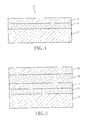
- FIG. 1is a pictorial representation (through a cross sectional view) illustrating an initial structure in which a first semiconductor layer having a first crystal orientation is formed on carrier wafer that includes an optional etch stop layer.
- FIG. 2is a pictorial representation (through a cross sectional view) illustrating a second semiconductor layer having a second crystal orientation that differs from the first crystal orientation formed on the substrate of FIG. 1 by wafer bonding.
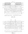
- FIG. 3is a pictorial representation (through a cross sectional view) illustrating a semiconductor material that is selectively grown from the first semiconductor layer though an opening where the second semiconductor layer and the sidewalls of the opening are covered by masking materials.
- FIG. 4is a pictorial representation (through a cross sectional view) illustrating a structure of FIG. 3 after the surface is planarized and the masking layer used during the semiconductor material growth is removed.
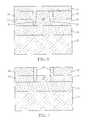
- FIG. 5is a pictorial representation (through a cross sectional view) illustrating a structure that is formed after an insulator layer is deposited and a handling wafer is bonded thereto.
- FIG. 6is a pictorial representation (through a cross sectional view) illustrating a structure after wafer flipping, and after the wafer carrier and the optional etch stop layer have been removed.
- FIG. 7is a pictorial representation (through a cross sectional view) illustrating a structure after the first semiconductor layer of the original structure has been removed and after the semiconductor material has been etched back to level out with the second semiconductor layer.
- FIG. 8is a pictorial representation (through a cross sectional view) illustrating a structure after the surface has been planarized by removing the optional insulator layer and after the spacers have been etched back.
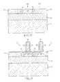
- FIG. 9is a pictorial representation (through a cross sectional view) illustrating a final structure of the present invention including an nFET and a pFET located on a surface with different crystal orientation, yet the same SOI thickness.
- FIG. 10is a pictorial representation (through a cross sectional view) illustrating a graded SiGe buffer layer and a strained Si layer grown on a semiconductor layer of a specific crystal orientation.
- FIG. 11is a pictorial representation (through a cross sectional view) illustrating a graded SiGe buffer layer and stained Si layer grown on a semiconductor layer of a specific crystal orientation that differs from the crystal orientation of the semiconductor layer of FIG. 10 .
- FIG. 12is a pictorial representation (through a cross sectional view) illustrating a structure after flip bonding of the structures of FIGS. 10 and 11 with a silicon handling wafer, and removal of the original carrier wafer, optional etch stop layer and the first semiconductor layer.
- FIG. 13is a pictorial representation (through a cross sectional view) illustrating a structure after the optional insulator layer and the second semiconductor layer are removed.
- FIG. 14is a pictorial representation (through a cross sectional view) illustrating a structure after the graded SiGe buffer layer is removed and after the spacer has been recessed.
- FIG. 15is a pictorial representation (through a cross sectional view) illustrating a structure after a masking cap is formed on top of the strained silicon.
- FIG. 16is a pictorial representation (through a cross sectional view) illustrating structure after a second graded SiGe buffer layer and stained silicon layer are selectively grown on a patterned substrate.
- the present inventionwhich provides a method of forming an SOI structure with the same thickness of the top SOI layer across the entire wafer where some area contains different crystal orientations and/or materials from the rest of the area, will now be described in greater detail by referring to the drawings that accompany the present application.
- like and corresponding elementsare referred to by like reference numerals.
- Initial substrate 10comprises a carrier wafer 12 , an optional etch stop layer 14 located on the carrier wafer 12 , and a first semiconductor layer 16 of a first crystal orientation on the optional etch stop layer 14 .
- the first semiconductor layer 16is located directly on the carrier wafer 12 .
- Carrier wafer 12is comprised of any semiconductor material including, for example, Si, SiC, SiGe, SiGeC, Ge alloys, GaAs, InAs, InP as well as other III/V or II/VI compound semiconductors.
- the thickness and crystal orientation of the carrier waferis inconsequential to the present invention.
- Optional etch stop layer 14may comprise an insulating material such as an oxide, nitride, oxynitride or any combination thereof, or, in some embodiments, the optional etch layer 14 may be a semiconductor material.
- the etch stop layer 14is optional as long as the carrier wafer 12 can be removed selectively from the first semiconductor layer 16 .
- the thickness of the optional etch stop layer 14may vary depending on the material and technique used in forming the same. Typically, however, the optional etch stop layer 14 has a thickness of from about 100 to about 1000 nm.
- the optional etch stop layer 14may be formed by a deposition process, including for example, chemical vapor deposition (CVD), plasma-enhanced chemical vapor deposition (PECVD), physical vapor deposition (PVP), or an epitaxial growth method, or by ion implantation and annealing.
- CVDchemical vapor deposition
- PECVDplasma-enhanced chemical vapor deposition
- PVPphysical vapor deposition
- epitaxial growth methodor by ion implantation and annealing.
- the first semiconductor layer 16is comprised of any semiconductor material including, for example, Si, SiC, SiGe, SiGeC, Ge alloys, GaAs, InAs, InP as well as other III/V or II/VI compound semiconductors.
- the optional etch stop layer 14is formed by ion implantation and annealing
- the first semiconductor layer 16is an SOI layer of a silicon-on-insulator structure.
- the first semiconductor layer 16has a first crystallographic orientation, which is preferably (100). Although a (100) crystal orientation is preferred, the first semiconductor layer 16 may have a (111), or a (110) crystallographic orientation.
- the thickness of the first semiconductor layer 16may vary depending on the technique used in fabricating the same. Typically, however, the first semiconductor layer 16 has a thickness of from about 5 to about 500 nm, with a thickness of from about 5 to about 100 nm being more highly preferred.
- the initial substrate 10 shown in FIG. 1is made using conventional processes well known to those skilled in the art.
- the initial substrate 10can be formed using various deposition techniques wherein layers 14 and 16 are grown or deposited on a surface of the carrier wafer 12 .
- the initial substrate 10can be formed using a separation by ion implantation of oxygen (SIMOX) process or wafer bonding and thinning by using a smart cut or other related thinning process.
- SIMOXion implantation of oxygen
- oxygen ionsare first implanted into a carrier wafer and then a buried oxide region is formed by annealing.
- the carrier wafer 12can be any material that can be bonded with the first semiconductor layer 16 and thereafter go through a subsequent high temperature process.
- a second semiconductor layer 20 having a second crystallographic orientation that differs from the first crystallographic orientation of the first semiconductor layer 16is applied to the structure shown in FIG. 1 .
- the second semiconductor layer 20may be formed directly atop the first semiconductor layer 16 , or as is shown in FIG. 2, an insulator 18 may be formed between the first semiconductor layer 16 and the second semiconductor layer 20 .
- the insulator 18is optional if the two semiconductor layers, i.e., layers 16 and 20 , can be directly bonded on top of each other and removed selectively from one another in a subsequent step.
- the structure with, or without, the optional insulator 18is formed utilizing a thermal bonding process followed by an optional thinning process.
- the bondingis achieved by first bringing two wafers into intimate contact with other; optionally applying an external force to the contacted wafers; and then heating the two contacted wafers under conditions that are capable of bonding the two wafers together.
- the two wafers used in fabricating the bonded structure shown in FIG. 2may include two SOI wafers, wherein one of the wafers includes the second semiconductor layer 20 and the other wafer, see FIG.
- the present inventionincludes the first semiconductor layer 16 ; an SOI wafer and a bulk semiconductor wafer; two bulk semiconductor wafers in which at least one of the wafers contains the insulating layer 18 thereon; or an SOI wafer and a bulk wafer which includes an ion implant region, such as a H 2 implant region, which can be used to split a portion of at least one of the wafers during bonding.
- the present inventionalso contemplates the use of two bulk wafers where one of the wafers has H 2 implanted therein.
- the heating step of the bonding processmay be performed in the presence or absence of an external force.
- the heating stepis typically performed in an inert ambient at a temperature of from about 600° to about 1300° C. for a time period of from about 2 to about 20 hours. More preferably, the bonding is performed at a temperature of from about 900° to about 1200° C. for a time period of from about 2 to about 20 hours.
- inert ambientis used in the present invention to denote an atmosphere in which an inert gas, such as He, Ar, N 2 , Xe, Kr or a mixture thereof, is employed.
- a preferred ambient used during the bonding processis N 2 .
- an initial heating stepthat is performed at a temperature of from about 200° to about 500° C. may be employed prior to the previously mentioned heating step.
- some material layers of at least one of the SOI wafersmay be removed after bonding utilizing a planarization process such as chemical mechanical polishing (CMP) or grinding and etching.
- CMPchemical mechanical polishing
- the ion implant regionforms a porous region during bonding which causes a portion of the wafer above the ion implant region to break off leaving a bonded wafer such as is shown, for example, in FIG. 2 .
- the implant regionis typically comprised of hydrogen ions that are implanted into the surface of the wafer utilizing ion implantation conditions that are well known to those skilled in the art.
- the optional insulator 18may have a variable thickness, but typically, the optional insulator 18 has a thickness of from about 100 to about 1000 nm. Insofar as the second semiconductor layer 20 is concerned, the thickness of that layer may also vary depending upon its origin. Typically, however, the second semiconductor layer 20 has a thickness of from about 10 to about 500 nm, with a thickness of from about 20 to about 100 nm being more highly preferred. As stated above, the second semiconductor layer 20 has a second crystallographic orientation that is different from the crystallographic orientation of the first semiconductor layer 16 . The second semiconductor layer 20 thus preferably has a (110) crystal orientation. Although a (110) crystal orientation is preferred, the second semiconductor layer 20 may have a (111), or a (100) crystallographic orientation depending on the crystallographic orientation of the first semiconductor layer 16 .
- semiconductor material layer 28is formed selectively on an exposed bottom surface of the first semiconductor layer 16 through an opening 25 .
- the structure including the semiconductor material layer 28is shown in FIG. 3 .
- the structure shown in FIG. 3also includes an optional pad layer 22 , patterned masking layer 24 , and spacers 26 .
- the structure shown in FIG. 3is formed by optionally forming pad layer 22 on an upper surface of the second semiconductor layer 20 by a thermal process, such as oxidation, or by a conventional deposition process such as chemical vapor deposition (CVD), plasma-enhanced CVD, atomic layer deposition, chemical solution deposition as well as other like deposition processes.
- the optional pad layer 22is comprised of an insulating material including, oxides, nitrides, oxynitrides or any combination thereof.
- the optional pad layer 22may have a variable thickness depending on the technique used in forming the same.
- the optional pad layer 22serves as an etch layer during the later removal of the patterned masking layer 24 .
- a patterned masking layer 24is then formed on a predetermined portion of the bonded structure so as to protect a portion (or portions) of the structure, while leaving at least one other portion of the bonded structure unprotected.
- the protected portions of the bonded structuredefine a first device region of the structure, whereas the unprotected portions of the bonded structure define a second device area.
- the patterned masking layer 24is a nitride or oxynitride layer that is formed and patterned utilizing lithography and etching.
- the structureis subjected to one or more etching steps so as to provide at least one opening (or trench) 25 that exposes a surface of the first semiconductor layer 16 .
- the one or more etching steps used at this point of the present inventionremove the unprotected portions of the optional pad layer 22 , as well as underlying portions of the second semiconductor layer 20 , and, if present, a portion of the insulator 18 .
- the etchingmay be performed utilizing a single etching process or multiple etching steps may be employed.
- the etching used at this point of the present inventionmay include a dry etching process such as reactive-ion etching, ion beam etching, plasma etching or laser etching, a wet etching process wherein a chemical etchant is employed or any combination thereof.
- the etchingmay stop on the upper surface of the first semiconductor layer 16 or it may stop at a region slightly below the upper surface of the first semiconductor layer 16 .
- reactive-ion etchingRIE is used in selectively removing the unprotected portions of the optional pad layer 22 , the second semiconductor layer 20 and, if present, the optional insulator 18 .
- the opening 25has exposed sidewalls after etching which include the remaining optional pad layer 22 , the remaining second semiconductor layer 20 , the remaining optional insulator 18 as well as the remaining first semiconductor layer 16 .
- the exposed sidewalls of layers 22 , 20 and 18are aligned with an outer most edge of patterned masking layer 24 .
- a spacer 26is formed on each of the exposed sidewalls in the at least one opening 25 .
- the spacer 26which is formed by deposition and etching, is comprised of an insulating material such as, for example, an oxide.
- the spacer 26is used in the present invention as a selective epitaxy block mask to block epitaxy from the second semiconductor layer 20 exposed on the etched sidewall to ensure high-quality single grain crystals in the etched area after epitaxy.
- a semiconductor material 28is formed selectively on the exposed surface of the first semiconductor layer 16 providing the structure shown, for example, in FIG. 3 .
- the semiconductor material 28has a crystallographic orientation that is the same as the crystallographic orientation of the first semiconductor layer 16 .
- the semiconductor material 28may comprise any Si-containing semiconductor, such as Si, strained Si, SiGe, SiC, SiGeC or combinations thereof, which is capable of being formed utilizing a selective epitaxial growth method.
- semiconductor material 28is comprised of Si.
- semiconductor material 28may be referred to as a regrown semiconductor material.
- the semiconductor material 28 formed by the epitaxy processmay be grown higher than the upper surface of the patterned masking layer 24 and then polished back to the upper surface of the patterned masking layer 24 to remove any possible facet growth.
- An upper surface of the semiconductor material 28can be recessed so as to be substantially level with an upper surface of the second semiconductor layer 20 . This recess may be achieved by utilizing a reactive ion etch process.
- the semiconductor material 28may be a different material from the fist semiconductor layer 16 .
- a SiGe alloymay be grown on a Si layer.
- the patterned masking layer 24 as well as the optional pad layer 22are removed from the structure to provide the structure shown, for example, in FIG. 4 .
- the spacer 26 on each of the trench sidewallscan be recessed somewhat below the surfaces of semiconductor layers 28 and 20 .
- the removal of the patterned masking layer 24is performed utilizing an etching process or by a chemical mechanical polishing (CMP) process. If present, the optional pad layer 22 is removed thereafter using an etching process that selectively removes the pad layer 22 as compared with semiconductor material.
- CMPchemical mechanical polishing
- Insulator layer 30is formed over the structure shown in FIG. 4 and thereafter that resultant structure is bonded to a handling wafer 32 so as to provide the structure shown, for example, in FIG. 5 .
- Insulator layer 30can comprise an oxide, nitride, oxynitride or any combination thereof.
- the insulator layer 30is an oxide such as, for example, SiO 2 .
- the insulator layer 30may be formed by deposition or, alternatively, a thermal growing process may be employed.
- the thickness of the insulator layer 30may vary, but typically the insulator layer 30 has a thickness of from about 100 to about 500 nm. In some instances, it may be necessary to polish the insulator layer 30 after its formation to ensure a flat surface for wafer bonding.
- Handling wafer 32may comprise the same or different semiconductor material as the carrier wafer 12 . Bonding is achieved using the aforementioned bonding process. The thickness of the handling wafer 32 is inconsequential to the present invention.
- the bonded structure shown in FIG. 5is flipped, top to bottom, such that the carrier wafer 12 is on top and the handling wafer 32 is on bottom.
- the carrier wafer 12 and, if present, the optional etch stop layer 14are removed providing the structure shown, for example, in FIG. 6 .
- a surface of fist semiconductor layer 16is exposed after flipping and removal of the carrier wafer 12 and the optional etch stop layer 14 .
- the removalis achieved utilizing one or more etching steps, planarization or a combination thereof.
- FIG. 7there is shown the structure that is formed after the first semiconductor layer 16 is removed from the structure illustrated in FIG. 6 .
- the first semiconductor layer 16is removed utilizing an etching process such as reactive-ion etching, ion beam etching, or plasma etching.
- the regrown semiconductor material 28is now etched back by a reactive-ion etching process so as to be level with the upper surface of second semiconductor layer 20 .
- the optional insulator 18is removed and the spacers 26 are recessed below the surfaces of semiconductor materials 20 and 28 to provide the structure shown, for example, in FIG. 8 .
- the removal of the optional insulator 18 and the recessing of the spacers 26are achieved utilizing the same or different etching process.
- first device regions labeled as 100 and a second device region labeled as 102are shown.
- the first device regionsinclude the second semiconductor layer 20
- the second device region 102includes the regrown semiconductor material 28 .
- Both active areasare SOI areas since an insulating layer 30 separates the active areas from the handling wafer 32 .
- the structure of FIG. 8contains the regrown semiconductor material 28 which is substantially coplanar and of substantially the same thickness as that of the second semiconductor layer 20 .
- the regrown semiconductor material 28has a different crystal orientation as compared with that of the second semiconductor layer 20 .
- an isolation region 34such as a shallow trench isolation region, is typically formed so as to isolate the first semiconductor device regions 100 from the second semiconductor device region 102 .
- the isolation regions 34replace the spacers 26 .
- spacers 26are used as the isolation region 34 .
- the isolation region 34is formed in the region in which the spacers are present utilizing processing steps that are well-known to those skilled in the art including, for example, trench definition and etching; optionally lining the trench with a diffusion barrier; and filling the trench with a trench dielectric such as an oxide. After the trench fill, the structure may be planarized and an optional densification process step may be performed to densify the trench dielectric.
- the resultant substantially planar structure containing isolation region 34is shown, for example, in FIG. 9 .
- This drawingalso shows the integrated structure that is formed after a first semiconductor device 50 is formed on a portion of the second semiconductor layer 20 and a second semiconductor device 52 is formed on the regrown semiconductor material 28 .
- the semiconductor devicesinclude gate dielectric 54 , gate conductor 56 and gate spacers 58 .
- the source/drain regionsare shown, but are not separately labeled.
- the semiconductor devicesare formed utilizing CMOS processing steps that are well known to those skilled in the art.
- the semiconductor devicesmay be nFETs or pFETs, with nFETs preferably being formed atop a semiconductor layer having a (100) crystal surface, while pFETs are preferably formed atop a semiconductor layer having a (110) crystal orientation.
- the present inventionalso contemplates an embodiment in which a strained-silicon-direct-on-insulator (SSDOI) structure with an nFET and pFET on different crystal orientations, but with the same SOI thickness across the wafer is formed.
- SSDOIstrained-silicon-direct-on-insulator
- the structure shown in FIG. 2is first provided utilizing the processing techniques described above.
- the structure shown in FIG. 2comprises carrier wafer 12 , optional etch stop layer 14 , first semiconductor layer 16 , optional insulator layer 18 and second semiconductor layer 20 .
- a first graded SiGe alloy layer 60is formed on top of the second semiconductor layer 20 .
- the first graded SiGe alloy layer 60is formed utilizing an epitaxial growth method.
- the thickness of the first graded SiGe alloy layer 60may vary depending on the conditions used during the epitaxial growth process and the Ge concentration. Typically, however, the first graded SiGe alloy layer 60 has a thickness of from about 100 to about 2000 nm.
- the Ge content in the first graded SiGe alloy layeris typically from 0 to about 50 atomic %
- a first strained Si layer 62 having a predetermined crystal orientationis formed on the graded SiGe alloy layer.
- the first strained Si layer 62is a thin layer having a thickness of about 30 nm or less depending on the magnitude of the strain. Typically, higher strained Si requires thin Si layers.
- the first strained Si layer 62is formed utilizing an epitaxial growth method that is capable of forming a strained Si layer. The resultant structure including first graded SiGe layer 60 and first strained Si layer 62 is illustrated in FIG. 10 .
- the structure shown in FIG. 11is provided utilizing similar processing steps used in forming the structure shown in FIG. 3 .
- the structure shown in FIG. 11includes a second graded SiGe alloy layer 66 and a second strained Si layer 68 that are formed selectively on an exposed surface of the first semiconductor layer 16 through an opening 25 .
- the structure shown in FIG. 11also includes an optional pad layer 22 , patterned masking layer 24 , and spacers 26 .
- the procedures used in forming the structure shown in FIG. 3are used in forming the structure shown in FIG. 11 except that the semiconductor material 28 used in FIG.
- the second graded SiGe alloy layer 66 and the second strained Si layer 68is replaced with the second graded SiGe alloy layer 66 and the second strained Si layer 68 .
- the second strained Si layer 68has a crystal orientation that differs from the first strained Si layer 62 .
- the Ge content in the second graded SiGe alloy layeris typically from 0 to 50 atomic %.
- the top surface of the second strained Si layer 68is substantially coplanar with the top surface of the first strained Si layer 62 .
- the second graded SiGe alloy layer 66may be grown higher than the upper surface of the patterned masking layer 24 , and then polished back to the upper surface of the patterned masking layer 24 .
- the second graded SiGe alloy layer 66may be recessed down to achieve a structure having a coplanar top surface of strained Si.
- FIG. 12shows the structure that is formed after insulator layer 30 formation on the surface of the structure shown in FIG. 11, bonding the insulator layer 30 to a handling wafer 32 , flipping the structure top to bottom and then removing the first semiconductor layer 16 .
- the processing stepsare the same as described above in connection with FIGS. 4-7.
- FIG. 13there is shown the resultant structure that is formed after optional insulator 18 and the second semiconductor layer 20 are removed from the structure.
- the removal of the optional insulator 18 and the second semiconductor layer 20is performed utilizing different etching processes in which the chemical etchant used in each etching process is selective for the specific material being removed.
- a surface of the first graded SiGe alloy layer 60is exposed after these removal steps.
- the first and second graded SiGe alloy layers 60 and 66are removed selective to the strained Si layers 62 and 68 .
- the spacers 26are recessed at this point of the present invention below the surfaces of strained Si layers 62 and 68 .
- a uniform SSDOI structurehas been obtained across the wafer having different crystal orientations.
- Semiconductor devicessuch as shown in FIG. 9 can be formed atop the different crystallographic planes.
- the first graded SiGe alloy layer 60 and the first strained Si layer 62are formed after providing the structure shown in FIG. 3 .
- the structure shown in FIG. 3is first provided and the layers 66 and 68 as well as masking cap 70 are formed so as to provide the structure shown, for example, in FIG. 15 .
- Layers 66 and 68are selectively grown atop the first semiconductor layer 16 .
- Masking cap 70which is typically comprised of an oxide, nitride or oxynitride is formed on the second strained Si layer 68 by deposition or a thermal process.
- the masking layer 24 and the spacer 26are used as selective epitaxy masks for the formation of the second graded SiGe alloy layer 66 and the second strained Si layer 68 .
- the masking cap 70 and the spacer 26are used as selective epitaxy masks for the formation of the first graded SiGe alloy layer 60 and the first strained Si layer 62 .).
- the structure including layers 66 and 68is shown, for example, in FIG. 16 .
- the first graded SiGe alloy layer 60 and the first strained Si layer 62are selectively grown on top of the second semiconductor layer 20 after removing the patterned masking layer 24 and the optional pad layer 22 .
- the remaining processing stepsare the same as the previously described SSDOI embodiment.
- the masking cap 70can be removed either before the wafer bonding steps of it can remain in the final structure.
Landscapes
- Engineering & Computer Science (AREA)
- Microelectronics & Electronic Packaging (AREA)
- Condensed Matter Physics & Semiconductors (AREA)
- General Physics & Mathematics (AREA)
- Manufacturing & Machinery (AREA)
- Computer Hardware Design (AREA)
- Physics & Mathematics (AREA)
- Power Engineering (AREA)
- Chemical & Material Sciences (AREA)
- Crystallography & Structural Chemistry (AREA)
- Recrystallisation Techniques (AREA)
- Metal-Oxide And Bipolar Metal-Oxide Semiconductor Integrated Circuits (AREA)
- Thin Film Transistor (AREA)
- Element Separation (AREA)
Abstract
Description
Claims (17)
Priority Applications (4)
| Application Number | Priority Date | Filing Date | Title |
|---|---|---|---|
| US10/647,395US6815278B1 (en) | 2003-08-25 | 2003-08-25 | Ultra-thin silicon-on-insulator and strained-silicon-direct-on-insulator with hybrid crystal orientations |
| CNB2004100578408ACN100339975C (en) | 2003-08-25 | 2004-08-19 | Manufacturing method of strained silicon-on-insulator |
| CNB200710109001XACN100505276C (en) | 2003-08-25 | 2004-08-19 | strained silicon insulator |
| US10/932,982US7098508B2 (en) | 2003-08-25 | 2004-09-02 | Ultra-thin silicon-on-insulator and strained-silicon-direct-on-insulator with hybrid crystal orientations |
Applications Claiming Priority (1)
| Application Number | Priority Date | Filing Date | Title |
|---|---|---|---|
| US10/647,395US6815278B1 (en) | 2003-08-25 | 2003-08-25 | Ultra-thin silicon-on-insulator and strained-silicon-direct-on-insulator with hybrid crystal orientations |
Related Child Applications (1)
| Application Number | Title | Priority Date | Filing Date |
|---|---|---|---|
| US10/932,982DivisionUS7098508B2 (en) | 2003-08-25 | 2004-09-02 | Ultra-thin silicon-on-insulator and strained-silicon-direct-on-insulator with hybrid crystal orientations |
Publications (1)
| Publication Number | Publication Date |
|---|---|
| US6815278B1true US6815278B1 (en) | 2004-11-09 |
Family
ID=33311117
Family Applications (2)
| Application Number | Title | Priority Date | Filing Date |
|---|---|---|---|
| US10/647,395Expired - LifetimeUS6815278B1 (en) | 2003-08-25 | 2003-08-25 | Ultra-thin silicon-on-insulator and strained-silicon-direct-on-insulator with hybrid crystal orientations |
| US10/932,982Expired - LifetimeUS7098508B2 (en) | 2003-08-25 | 2004-09-02 | Ultra-thin silicon-on-insulator and strained-silicon-direct-on-insulator with hybrid crystal orientations |
Family Applications After (1)
| Application Number | Title | Priority Date | Filing Date |
|---|---|---|---|
| US10/932,982Expired - LifetimeUS7098508B2 (en) | 2003-08-25 | 2004-09-02 | Ultra-thin silicon-on-insulator and strained-silicon-direct-on-insulator with hybrid crystal orientations |
Country Status (2)
| Country | Link |
|---|---|
| US (2) | US6815278B1 (en) |
| CN (2) | CN100339975C (en) |
Cited By (60)
| Publication number | Priority date | Publication date | Assignee | Title |
|---|---|---|---|---|
| US20030168165A1 (en)* | 2002-03-08 | 2003-09-11 | Hatfield Stephen F. | Hot melt pressure sensitive adhesives for disposable articles |
| US20050116290A1 (en)* | 2003-12-02 | 2005-06-02 | De Souza Joel P. | Planar substrate with selected semiconductor crystal orientations formed by localized amorphization and recrystallization of stacked template layers |
| US20050181549A1 (en)* | 2004-02-17 | 2005-08-18 | Barr Alexander L. | Semiconductor structure having strained semiconductor and method therefor |
| US20060063368A1 (en)* | 2004-09-17 | 2006-03-23 | Shashank Sharma | Reduction of a feature dimension in a nano-scale device |
| US20060084244A1 (en)* | 2003-04-04 | 2006-04-20 | Yee-Chia Yeo | Silicon-on-insulator chip with multiple crystal orientations |
| US20060105533A1 (en)* | 2004-11-16 | 2006-05-18 | Chong Yung F | Method for engineering hybrid orientation/material semiconductor substrate |
| US20060108643A1 (en)* | 2003-10-29 | 2006-05-25 | International Business Machines Corporation | CMOS on hybrid substrate with different crystal orientations using silicon-to-silicon direct wafer bonding |
| US20060113629A1 (en)* | 2004-11-30 | 2006-06-01 | Andy Wei | Technique for forming a substrate having crystalline semiconductor regions of different characteristics located above a crystalline bulk substrate |
| US20060226491A1 (en)* | 2005-04-06 | 2006-10-12 | International Business Machines Corporation | Inverted multilayer semiconductor device assembly |
| US20060244068A1 (en)* | 2005-04-27 | 2006-11-02 | International Business Machines Corporation | Field effect transistor with mixed-crystal-orientation channel and source/drain regions |
| US20060286781A1 (en)* | 2005-06-16 | 2006-12-21 | International Business Machines Corporation | Crystal imprinting methods for fabricating subsrates with thin active silicon layers |
| US20060284250A1 (en)* | 2005-06-16 | 2006-12-21 | International Business Machines Corporation | Hybrid oriented substrates and crystal imprinting methods for forming such hybrid oriented substrates |
| US20060284251A1 (en)* | 2005-06-16 | 2006-12-21 | International Business Machines Corporation | Coplanar silicon-on-insulator (SOI) regions of different crystal orientations and methods of making the same |
| US20060286778A1 (en)* | 2005-06-21 | 2006-12-21 | International Business Machines Corporation | Method of manufacturing dual orientation wafers |
| US20060292834A1 (en)* | 2005-06-24 | 2006-12-28 | Taiwan Semiconductor Manufacturing Company, Ltd. | High performance transistors with hybrid crystal orientations |
| US20070029553A1 (en)* | 2005-08-08 | 2007-02-08 | North Carolina State University | Methods of fabricating strained semiconductor-on-insulator field-effect transistors and related devices |
| US20070034950A1 (en)* | 2005-08-09 | 2007-02-15 | Samsung Electronics Co., Ltd. | Semiconductor wafer and method of fabricating the same |
| US20070096206A1 (en)* | 2005-11-03 | 2007-05-03 | International Business Machines Corporation | Gate electrode stress control for finfet performance enhancement |
| US20070096170A1 (en)* | 2005-11-02 | 2007-05-03 | International Business Machines Corporation | Low modulus spacers for channel stress enhancement |
| US20070102769A1 (en)* | 2005-11-08 | 2007-05-10 | Taiwan Semiconductor Manufacturing Company, Ltd. | Dual SOI structure |
| US20070120154A1 (en)* | 2005-11-30 | 2007-05-31 | International Business Machines Corporation | Finfet structure with multiply stressed gate electrode |
| US20070122965A1 (en)* | 2005-09-29 | 2007-05-31 | International Business Machines Corporation | Stress engineering using dual pad nitride with selective soi device architecture |
| US20070145481A1 (en)* | 2005-12-22 | 2007-06-28 | Armin Tilke | Silicon-on-insulator chip having multiple crystal orientations |
| US20070158743A1 (en)* | 2006-01-11 | 2007-07-12 | International Business Machines Corporation | Thin silicon single diffusion field effect transistor for enhanced drive performance with stress film liners |
| US20070202635A1 (en)* | 2006-02-27 | 2007-08-30 | Ellis-Monaghan John J | Multi-orientation semiconductor-on-insulator (soi) substrate, and method of fabricating same |
| US20070218654A1 (en)* | 2006-03-14 | 2007-09-20 | Spencer Gregory S | Silicon deposition over dual surface orientation substrates to promote uniform polishing |
| US20070218659A1 (en)* | 2006-03-14 | 2007-09-20 | Spencer Gregory S | Selective silicon deposition for planarized dual surface orientation integration |
| US20070267723A1 (en)* | 2006-05-16 | 2007-11-22 | Kerry Bernstein | Double-sided integrated circuit chips |
| US20070267634A1 (en)* | 2006-05-19 | 2007-11-22 | International Business Machines Corporation | Hybrid strained orientated substrates and devices |
| US20070281436A1 (en)* | 2006-05-31 | 2007-12-06 | Sadaka Mariam G | Trench liner for DSO integration |
| US20080087961A1 (en)* | 2006-10-11 | 2008-04-17 | International Business Machines Corporation | Method of reducing stacking faults through annealing |
| US20080173901A1 (en)* | 2007-01-18 | 2008-07-24 | International Business Machines Corporation | Cmos devices having channel regions with a v-shaped trench and hybrid channel orientations, and method for forming the same |
| US20080220280A1 (en)* | 2007-03-06 | 2008-09-11 | Hsu Louis C | Defect-free hybrid orientation technology for semiconductor devices |
| FR2913815A1 (en)* | 2007-06-06 | 2008-09-19 | Soitec Silicon On Insulator | Hybrid substrate manufacturing method for telecommunication network, involves forming dielectric/polymer layer on structure, assembling layer with support substrates, and eliminating initial substrate until buried layer is eliminated |
| CN100424824C (en)* | 2005-01-18 | 2008-10-08 | 国际商业机器公司 | Method of forming semiconductor substrate |
| CN100428475C (en)* | 2005-01-05 | 2008-10-22 | 国际商业机器公司 | Semiconductor structure with enhanced carrier mobility and method of manufacturing the same |
| US20080274595A1 (en)* | 2007-05-01 | 2008-11-06 | Spencer Gregory S | Dual substrate orientation or bulk on SOI integrations using oxidation for silicon epitaxy spacer formation |
| US20080286888A1 (en)* | 2007-05-18 | 2008-11-20 | International Business Machines Corporation | Test structures and methodology for detecting hot defects |
| FR2917235A1 (en)* | 2007-06-06 | 2008-12-12 | Soitec Silicon On Insulator | METHOD FOR PRODUCING HYBRID COMPONENTS |
| CN100466267C (en)* | 2005-07-15 | 2009-03-04 | 国际商业机器公司 | Semiconductor structure and manufacturing method thereof |
| CN100479161C (en)* | 2005-02-01 | 2009-04-15 | 国际商业机器公司 | Semiconductor device and method of manufacturing same |
| US7528027B1 (en) | 2008-03-25 | 2009-05-05 | International Business Machines Corporation | Structure and method for manufacturing device with ultra thin SOI at the tip of a V-shape channel |
| US20090121260A1 (en)* | 2007-11-14 | 2009-05-14 | Kerry Bernstein | Double-sided integrated circuit chips |
| DE102004060961B4 (en)* | 2004-12-17 | 2010-06-02 | Advanced Micro Devices, Inc., Sunnyvale | A method of manufacturing a hybrid semiconductor substrate over a buried insulating layer |
| US20100200896A1 (en)* | 2009-02-09 | 2010-08-12 | International Business Machines Corporation | Embedded stress elements on surface thin direct silicon bond substrates |
| US7790540B2 (en) | 2006-08-25 | 2010-09-07 | International Business Machines Corporation | Structure and method to use low k stress liner to reduce parasitic capacitance |
| US20100244139A1 (en)* | 2004-06-24 | 2010-09-30 | International Business Machines Corporation | Strained-silicon cmos device and method |
| US7863197B2 (en) | 2006-01-09 | 2011-01-04 | International Business Machines Corporation | Method of forming a cross-section hourglass shaped channel region for charge carrier mobility modification |
| US7935993B2 (en) | 2006-01-10 | 2011-05-03 | International Business Machines Corporation | Semiconductor device structure having enhanced performance FET device |
| US20110175164A1 (en)* | 2010-01-19 | 2011-07-21 | International Business Machines Corporation | Device structure, layout and fabrication method for uniaxially strained transistors |
| US20110175166A1 (en)* | 2010-01-19 | 2011-07-21 | International Business Machines Corporation | Strained cmos device, circuit and method of fabrication |
| US8053304B2 (en)* | 2009-02-24 | 2011-11-08 | Taiwan Semiconductor Manufacturing Company, Ltd. | Method of forming high-mobility devices including epitaxially growing a semiconductor layer on a dislocation-blocking layer in a recess formed in a semiconductor substrate |
| DE112005003123B4 (en)* | 2004-12-08 | 2011-11-10 | Globalfoundries Inc. | A semiconductor device and method of making a semiconductor device having a plurality of stacked hybrid orientation layers |
| US8093084B2 (en) | 2009-04-30 | 2012-01-10 | Freescale Semiconductor, Inc. | Semiconductor device with photonics |
| US8569159B2 (en) | 2008-02-28 | 2013-10-29 | International Business Machines Corporation | CMOS structure including non-planar hybrid orientation substrate with planar gate electrodes and method for fabrication |
| US8598006B2 (en) | 2010-03-16 | 2013-12-03 | International Business Machines Corporation | Strain preserving ion implantation methods |
| US8629501B2 (en) | 2007-09-25 | 2014-01-14 | International Business Machines Corporation | Stress-generating structure for semiconductor-on-insulator devices |
| US8728905B2 (en) | 2007-11-15 | 2014-05-20 | International Business Machines Corporation | Stress-generating shallow trench isolation structure having dual composition |
| US9105689B1 (en) | 2014-03-24 | 2015-08-11 | Silanna Semiconductor U.S.A., Inc. | Bonded semiconductor structure with SiGeC layer as etch stop |
| US9269608B2 (en)* | 2014-03-24 | 2016-02-23 | Qualcomm Switch Corp. | Bonded semiconductor structure with SiGeC/SiGeBC layer as etch stop |
Families Citing this family (42)
| Publication number | Priority date | Publication date | Assignee | Title |
|---|---|---|---|---|
| JP4267266B2 (en)* | 2001-07-10 | 2009-05-27 | 株式会社半導体エネルギー研究所 | Method for manufacturing semiconductor device |
| US6830962B1 (en)* | 2003-08-05 | 2004-12-14 | International Business Machines Corporation | Self-aligned SOI with different crystal orientation using wafer bonding and SIMOX processes |
| US8450806B2 (en)* | 2004-03-31 | 2013-05-28 | International Business Machines Corporation | Method for fabricating strained silicon-on-insulator structures and strained silicon-on insulator structures formed thereby |
| US7393733B2 (en) | 2004-12-01 | 2008-07-01 | Amberwave Systems Corporation | Methods of forming hybrid fin field-effect transistor structures |
| US7282425B2 (en)* | 2005-01-31 | 2007-10-16 | International Business Machines Corporation | Structure and method of integrating compound and elemental semiconductors for high-performance CMOS |
| WO2006103491A1 (en)* | 2005-03-29 | 2006-10-05 | S.O.I.Tec Silicon On Insulator Technologies | Hybrid fully soi-type multilayer structure |
| US9153645B2 (en) | 2005-05-17 | 2015-10-06 | Taiwan Semiconductor Manufacturing Company, Ltd. | Lattice-mismatched semiconductor structures with reduced dislocation defect densities and related methods for device fabrication |
| US8324660B2 (en) | 2005-05-17 | 2012-12-04 | Taiwan Semiconductor Manufacturing Company, Ltd. | Lattice-mismatched semiconductor structures with reduced dislocation defect densities and related methods for device fabrication |
| KR101329388B1 (en) | 2005-07-26 | 2013-11-14 | 앰버웨이브 시스템즈 코포레이션 | Solutions for integrated circuit integration of alternative active area materials |
| US7638842B2 (en) | 2005-09-07 | 2009-12-29 | Amberwave Systems Corporation | Lattice-mismatched semiconductor structures on insulators |
| US7605447B2 (en)* | 2005-09-22 | 2009-10-20 | International Business Machines Corporation | Highly manufacturable SRAM cells in substrates with hybrid crystal orientation |
| US8441000B2 (en)* | 2006-02-01 | 2013-05-14 | International Business Machines Corporation | Heterojunction tunneling field effect transistors, and methods for fabricating the same |
| WO2007112066A2 (en) | 2006-03-24 | 2007-10-04 | Amberwave Systems Corporation | Lattice-mismatched semiconductor structures and related methods for device fabrication |
| US20070252216A1 (en)* | 2006-04-28 | 2007-11-01 | Infineon Technologies Ag | Semiconductor device and a method of manufacturing such a semiconductor device |
| US7435639B2 (en)* | 2006-05-31 | 2008-10-14 | Freescale Semiconductor, Inc. | Dual surface SOI by lateral epitaxial overgrowth |
| US8173551B2 (en) | 2006-09-07 | 2012-05-08 | Taiwan Semiconductor Manufacturing Co., Ltd. | Defect reduction using aspect ratio trapping |
| WO2008039495A1 (en) | 2006-09-27 | 2008-04-03 | Amberwave Systems Corporation | Tri-gate field-effect transistors formed by aspect ratio trapping |
| WO2008039534A2 (en) | 2006-09-27 | 2008-04-03 | Amberwave Systems Corporation | Quantum tunneling devices and circuits with lattice- mismatched semiconductor structures |
| US8502263B2 (en) | 2006-10-19 | 2013-08-06 | Taiwan Semiconductor Manufacturing Company, Ltd. | Light-emitter-based devices with lattice-mismatched semiconductor structures |
| WO2008124154A2 (en) | 2007-04-09 | 2008-10-16 | Amberwave Systems Corporation | Photovoltaics on silicon |
| US7825328B2 (en) | 2007-04-09 | 2010-11-02 | Taiwan Semiconductor Manufacturing Company, Ltd. | Nitride-based multi-junction solar cell modules and methods for making the same |
| US8304805B2 (en) | 2009-01-09 | 2012-11-06 | Taiwan Semiconductor Manufacturing Company, Ltd. | Semiconductor diodes fabricated by aspect ratio trapping with coalesced films |
| US8237151B2 (en) | 2009-01-09 | 2012-08-07 | Taiwan Semiconductor Manufacturing Company, Ltd. | Diode-based devices and methods for making the same |
| US7547641B2 (en)* | 2007-06-05 | 2009-06-16 | International Business Machines Corporation | Super hybrid SOI CMOS devices |
| US8329541B2 (en) | 2007-06-15 | 2012-12-11 | Taiwan Semiconductor Manufacturing Company, Ltd. | InP-based transistor fabrication |
| JP2010538495A (en) | 2007-09-07 | 2010-12-09 | アンバーウェーブ・システムズ・コーポレーション | Multi-junction solar cell |
| US8039401B2 (en)* | 2007-12-14 | 2011-10-18 | Fairchild Semiconductor Corporation | Structure and method for forming hybrid substrate |
| US8183667B2 (en) | 2008-06-03 | 2012-05-22 | Taiwan Semiconductor Manufacturing Co., Ltd. | Epitaxial growth of crystalline material |
| US8274097B2 (en) | 2008-07-01 | 2012-09-25 | Taiwan Semiconductor Manufacturing Company, Ltd. | Reduction of edge effects from aspect ratio trapping |
| US8981427B2 (en) | 2008-07-15 | 2015-03-17 | Taiwan Semiconductor Manufacturing Company, Ltd. | Polishing of small composite semiconductor materials |
| EP2335273A4 (en) | 2008-09-19 | 2012-01-25 | Taiwan Semiconductor Mfg | FORMATION OF DEVICES BY GROWTH OF EPITAXIAL LAYERS |
| US20100072515A1 (en) | 2008-09-19 | 2010-03-25 | Amberwave Systems Corporation | Fabrication and structures of crystalline material |
| US8253211B2 (en) | 2008-09-24 | 2012-08-28 | Taiwan Semiconductor Manufacturing Company, Ltd. | Semiconductor sensor structures with reduced dislocation defect densities |
| US8629446B2 (en) | 2009-04-02 | 2014-01-14 | Taiwan Semiconductor Manufacturing Company, Ltd. | Devices formed from a non-polar plane of a crystalline material and method of making the same |
| US8242510B2 (en)* | 2010-01-28 | 2012-08-14 | Intersil Americas Inc. | Monolithic integration of gallium nitride and silicon devices and circuits, structure and method |
| CN101986435B (en)* | 2010-06-25 | 2012-12-19 | 中国科学院上海微系统与信息技术研究所 | Manufacturing method of metal oxide semiconductor (MOS) device structure for preventing floating body and self-heating effect |
| US8643061B2 (en)* | 2010-10-20 | 2014-02-04 | International Business Machines Corporation | Structure of high-K metal gate semiconductor transistor |
| US8492237B2 (en) | 2011-03-08 | 2013-07-23 | International Business Machines Corporation | Methods of fabricating a bipolar junction transistor with a self-aligned emitter and base |
| US8685804B2 (en) | 2011-10-03 | 2014-04-01 | International Business Machines Corporation | Enhancement of charge carrier mobility in transistors |
| FR3051596B1 (en) | 2016-05-17 | 2022-11-18 | Soitec Silicon On Insulator | METHOD FOR MANUFACTURING A STRESSED-ON-INSULATOR SEMICONDUCTOR-TYPE SUBSTRATE |
| JP6763703B2 (en)* | 2016-06-17 | 2020-09-30 | ラピスセミコンダクタ株式会社 | Semiconductor devices and methods for manufacturing semiconductor devices |
| US11798991B2 (en)* | 2019-06-28 | 2023-10-24 | Intel Corporation | Amorphization and regrowth of source-drain regions from the bottom-side of a semiconductor assembly |
Citations (2)
| Publication number | Priority date | Publication date | Assignee | Title |
|---|---|---|---|---|
| US5296403A (en)* | 1990-01-31 | 1994-03-22 | Research Development Corp. Of Japan | Method of manufacturing a static induction field-effect transistor |
| US6670694B2 (en)* | 2001-05-31 | 2003-12-30 | Kabushiki Kaisha Toshiba | Semiconductor device |
Family Cites Families (15)
| Publication number | Priority date | Publication date | Assignee | Title |
|---|---|---|---|---|
| US4768076A (en)* | 1984-09-14 | 1988-08-30 | Hitachi, Ltd. | Recrystallized CMOS with different crystal planes |
| JPH01162376A (en)* | 1987-12-18 | 1989-06-26 | Fujitsu Ltd | Manufacture of semiconductor device |
| JPH0697401A (en)* | 1991-07-12 | 1994-04-08 | Seijirou Furukawa | Semiconductor device and manufacturing method thereof |
| US5532511A (en)* | 1992-10-23 | 1996-07-02 | Research Development Corp. Of Japan | Semiconductor device comprising a highspeed static induction transistor |
| JPH09246505A (en)* | 1996-03-01 | 1997-09-19 | Hitachi Ltd | Semiconductor integrated circuit device |
| US5963817A (en)* | 1997-10-16 | 1999-10-05 | International Business Machines Corporation | Bulk and strained silicon on insulator using local selective oxidation |
| JP3804375B2 (en)* | 1999-12-09 | 2006-08-02 | 株式会社日立製作所 | Semiconductor device and power switching drive system using the same |
| JP2002158357A (en)* | 2000-11-16 | 2002-05-31 | Sony Corp | Soi semiconductor device and its manufacturing method |
| JP3669491B2 (en)* | 2001-03-29 | 2005-07-06 | 独立行政法人産業技術総合研究所 | Negative resistance field effect element |
| US6603156B2 (en)* | 2001-03-31 | 2003-08-05 | International Business Machines Corporation | Strained silicon on insulator structures |
| US6903384B2 (en)* | 2003-01-15 | 2005-06-07 | Sharp Laboratories Of America, Inc. | System and method for isolating silicon germanium dislocation regions in strained-silicon CMOS applications |
| US7157774B2 (en)* | 2003-01-31 | 2007-01-02 | Taiwan Semiconductor Manufacturing Co., Ltd. | Strained silicon-on-insulator transistors with mesa isolation |
| US6803270B2 (en)* | 2003-02-21 | 2004-10-12 | International Business Machines Corporation | CMOS performance enhancement using localized voids and extended defects |
| US6911379B2 (en)* | 2003-03-05 | 2005-06-28 | Taiwan Semiconductor Manufacturing Company, Ltd. | Method of forming strained silicon on insulator substrate |
| US6902962B2 (en)* | 2003-04-04 | 2005-06-07 | Taiwan Semiconductor Manufacturing Company, Ltd. | Silicon-on-insulator chip with multiple crystal orientations |
- 2003
- 2003-08-25USUS10/647,395patent/US6815278B1/ennot_activeExpired - Lifetime
- 2004
- 2004-08-19CNCNB2004100578408Apatent/CN100339975C/ennot_activeExpired - Fee Related
- 2004-08-19CNCNB200710109001XApatent/CN100505276C/ennot_activeExpired - Fee Related
- 2004-09-02USUS10/932,982patent/US7098508B2/ennot_activeExpired - Lifetime
Patent Citations (2)
| Publication number | Priority date | Publication date | Assignee | Title |
|---|---|---|---|---|
| US5296403A (en)* | 1990-01-31 | 1994-03-22 | Research Development Corp. Of Japan | Method of manufacturing a static induction field-effect transistor |
| US6670694B2 (en)* | 2001-05-31 | 2003-12-30 | Kabushiki Kaisha Toshiba | Semiconductor device |
Cited By (132)
| Publication number | Priority date | Publication date | Assignee | Title |
|---|---|---|---|---|
| US20030168165A1 (en)* | 2002-03-08 | 2003-09-11 | Hatfield Stephen F. | Hot melt pressure sensitive adhesives for disposable articles |
| US7704809B2 (en) | 2003-04-04 | 2010-04-27 | Taiwan Semiconductor Manufacturing Company, Ltd. | Silicon-on-insulator chip with multiple crystal orientations |
| US20080160727A1 (en)* | 2003-04-04 | 2008-07-03 | Yee-Chia Yeo | Silicon-on-Insulator Chip with Multiple Crystal Orientations |
| US7368334B2 (en)* | 2003-04-04 | 2008-05-06 | Taiwan Semiconductor Manufacturing Company, Ltd. | Silicon-on-insulator chip with multiple crystal orientations |
| US20060084244A1 (en)* | 2003-04-04 | 2006-04-20 | Yee-Chia Yeo | Silicon-on-insulator chip with multiple crystal orientations |
| US7364958B2 (en)* | 2003-10-29 | 2008-04-29 | International Business Machines Corporation | CMOS on hybrid substrate with different crystal orientations using silicon-to-silicon direct wafer bonding |
| US20060108643A1 (en)* | 2003-10-29 | 2006-05-25 | International Business Machines Corporation | CMOS on hybrid substrate with different crystal orientations using silicon-to-silicon direct wafer bonding |
| US20080108184A1 (en)* | 2003-12-02 | 2008-05-08 | International Business Machines Corporation | Planar substrate with selected semiconductor crystal orientations formed by localized amorphization and recrystallization of stacked template layers |
| US7785939B2 (en) | 2003-12-02 | 2010-08-31 | International Business Machines Corporation | Planar substrate with selected semiconductor crystal orientations formed by localized amorphization and recrystallization of stacked template layers |
| US20050116290A1 (en)* | 2003-12-02 | 2005-06-02 | De Souza Joel P. | Planar substrate with selected semiconductor crystal orientations formed by localized amorphization and recrystallization of stacked template layers |
| WO2005081748A3 (en)* | 2004-02-17 | 2006-06-08 | Freescale Semiconductor Inc | Semiconductor structure having strained semiconductor and method therefor |
| US20050181549A1 (en)* | 2004-02-17 | 2005-08-18 | Barr Alexander L. | Semiconductor structure having strained semiconductor and method therefor |
| US7205210B2 (en)* | 2004-02-17 | 2007-04-17 | Freescale Semiconductor, Inc. | Semiconductor structure having strained semiconductor and method therefor |
| US20100244139A1 (en)* | 2004-06-24 | 2010-09-30 | International Business Machines Corporation | Strained-silicon cmos device and method |
| US20060063368A1 (en)* | 2004-09-17 | 2006-03-23 | Shashank Sharma | Reduction of a feature dimension in a nano-scale device |
| US7189635B2 (en)* | 2004-09-17 | 2007-03-13 | Hewlett-Packard Development Company, L.P. | Reduction of a feature dimension in a nano-scale device |
| US20060105533A1 (en)* | 2004-11-16 | 2006-05-18 | Chong Yung F | Method for engineering hybrid orientation/material semiconductor substrate |
| US20060113629A1 (en)* | 2004-11-30 | 2006-06-01 | Andy Wei | Technique for forming a substrate having crystalline semiconductor regions of different characteristics located above a crystalline bulk substrate |
| US7381624B2 (en)* | 2004-11-30 | 2008-06-03 | Advanced Micro Devices, Inc. | Technique for forming a substrate having crystalline semiconductor regions of different characteristics located above a crystalline bulk substrate |
| DE112005003123B4 (en)* | 2004-12-08 | 2011-11-10 | Globalfoundries Inc. | A semiconductor device and method of making a semiconductor device having a plurality of stacked hybrid orientation layers |
| DE102004060961B4 (en)* | 2004-12-17 | 2010-06-02 | Advanced Micro Devices, Inc., Sunnyvale | A method of manufacturing a hybrid semiconductor substrate over a buried insulating layer |
| CN100428475C (en)* | 2005-01-05 | 2008-10-22 | 国际商业机器公司 | Semiconductor structure with enhanced carrier mobility and method of manufacturing the same |
| CN100424824C (en)* | 2005-01-18 | 2008-10-08 | 国际商业机器公司 | Method of forming semiconductor substrate |
| CN100479161C (en)* | 2005-02-01 | 2009-04-15 | 国际商业机器公司 | Semiconductor device and method of manufacturing same |
| US20060226491A1 (en)* | 2005-04-06 | 2006-10-12 | International Business Machines Corporation | Inverted multilayer semiconductor device assembly |
| US7547917B2 (en) | 2005-04-06 | 2009-06-16 | International Business Machines Corporation | Inverted multilayer semiconductor device assembly |
| US7465992B2 (en)* | 2005-04-27 | 2008-12-16 | International Business Machines Corporation | Field effect transistor with mixed-crystal-orientation channel and source/drain regions |
| US20060244068A1 (en)* | 2005-04-27 | 2006-11-02 | International Business Machines Corporation | Field effect transistor with mixed-crystal-orientation channel and source/drain regions |
| US7875960B2 (en) | 2005-06-16 | 2011-01-25 | International Business Machines Corporation | Hybrid oriented substrates and crystal imprinting methods for forming such hybrid oriented substrates |
| US7393730B2 (en) | 2005-06-16 | 2008-07-01 | International Business Machines Corporation | Coplanar silicon-on-insulator (SOI) regions of different crystal orientations and methods of making the same |
| US7525121B2 (en) | 2005-06-16 | 2009-04-28 | International Business Machines Corporation | Coplanar silicon-on-insulator (SOI) regions of different crystal orientations and methods of making the same |
| US20060286781A1 (en)* | 2005-06-16 | 2006-12-21 | International Business Machines Corporation | Crystal imprinting methods for fabricating subsrates with thin active silicon layers |
| US7473985B2 (en) | 2005-06-16 | 2009-01-06 | International Business Machines Corporation | Hybrid oriented substrates and crystal imprinting methods for forming such hybrid oriented substrates |
| US20060284250A1 (en)* | 2005-06-16 | 2006-12-21 | International Business Machines Corporation | Hybrid oriented substrates and crystal imprinting methods for forming such hybrid oriented substrates |
| US7651929B2 (en) | 2005-06-16 | 2010-01-26 | International Business Machines Corporation | Hybrid oriented substrates and crystal imprinting methods for forming such hybrid oriented substrates |
| US20080050890A1 (en)* | 2005-06-16 | 2008-02-28 | International Business Machines Corporation | Hybrid oriented substrates and crystal imprinting methods for forming such hybrid oriented substrates |
| US20080050891A1 (en)* | 2005-06-16 | 2008-02-28 | Ibm | Coplanar silicon-on-insulator (soi) regions of different crystal orientations and methods of making the same |
| US20080283920A1 (en)* | 2005-06-16 | 2008-11-20 | International Business Machines Corporation | Hybrid oriented substrates and crystal imprinting methods for forming such hybrid oriented substrates |
| US7358164B2 (en) | 2005-06-16 | 2008-04-15 | International Business Machines Corporation | Crystal imprinting methods for fabricating substrates with thin active silicon layers |
| US20060284251A1 (en)* | 2005-06-16 | 2006-12-21 | International Business Machines Corporation | Coplanar silicon-on-insulator (SOI) regions of different crystal orientations and methods of making the same |
| US7439108B2 (en) | 2005-06-16 | 2008-10-21 | International Business Machines Corporation | Coplanar silicon-on-insulator (SOI) regions of different crystal orientations and methods of making the same |
| US20080146006A1 (en)* | 2005-06-16 | 2008-06-19 | International Business Machines Corporation | Crystal imprinting methods for fabricating substrates with thin active silicon layers |
| US7803700B2 (en) | 2005-06-16 | 2010-09-28 | International Business Machines Corporation | Crystal imprinting methods for fabricating substrates with thin active silicon layers |
| US7799609B2 (en) | 2005-06-21 | 2010-09-21 | International Business Machines Corporation | Method of manufacturing dual orientation wafers |
| US7344962B2 (en) | 2005-06-21 | 2008-03-18 | International Business Machines Corporation | Method of manufacturing dual orientation wafers |
| US20080096370A1 (en)* | 2005-06-21 | 2008-04-24 | International Business Machines Corporation | Method of manufacturing dual orientation wafers |
| US20060286778A1 (en)* | 2005-06-21 | 2006-12-21 | International Business Machines Corporation | Method of manufacturing dual orientation wafers |
| US7611937B2 (en) | 2005-06-24 | 2009-11-03 | Taiwan Semiconductor Manufacturing Company, Ltd. | High performance transistors with hybrid crystal orientations |
| US20060292834A1 (en)* | 2005-06-24 | 2006-12-28 | Taiwan Semiconductor Manufacturing Company, Ltd. | High performance transistors with hybrid crystal orientations |
| CN100466267C (en)* | 2005-07-15 | 2009-03-04 | 国际商业机器公司 | Semiconductor structure and manufacturing method thereof |
| US20070029553A1 (en)* | 2005-08-08 | 2007-02-08 | North Carolina State University | Methods of fabricating strained semiconductor-on-insulator field-effect transistors and related devices |
| US7211458B2 (en)* | 2005-08-08 | 2007-05-01 | North Carolina State University | Methods of fabricating strained semiconductor-on-insulator field-effect transistors and related devices |
| US20070034950A1 (en)* | 2005-08-09 | 2007-02-15 | Samsung Electronics Co., Ltd. | Semiconductor wafer and method of fabricating the same |
| US7675091B2 (en)* | 2005-08-09 | 2010-03-09 | Samsung Electronics Co., Ltd. | Semiconductor wafer and method of fabricating the same |
| US7550364B2 (en) | 2005-09-29 | 2009-06-23 | International Business Machines Corporation | Stress engineering using dual pad nitride with selective SOI device architecture |
| US20070122965A1 (en)* | 2005-09-29 | 2007-05-31 | International Business Machines Corporation | Stress engineering using dual pad nitride with selective soi device architecture |
| US20070096170A1 (en)* | 2005-11-02 | 2007-05-03 | International Business Machines Corporation | Low modulus spacers for channel stress enhancement |
| US20070096206A1 (en)* | 2005-11-03 | 2007-05-03 | International Business Machines Corporation | Gate electrode stress control for finfet performance enhancement |
| US7655511B2 (en) | 2005-11-03 | 2010-02-02 | International Business Machines Corporation | Gate electrode stress control for finFET performance enhancement |
| US7960801B2 (en) | 2005-11-03 | 2011-06-14 | International Business Machines Corporation | Gate electrode stress control for finFET performance enhancement description |
| US20070102769A1 (en)* | 2005-11-08 | 2007-05-10 | Taiwan Semiconductor Manufacturing Company, Ltd. | Dual SOI structure |
| US7986029B2 (en)* | 2005-11-08 | 2011-07-26 | Taiwan Semiconductor Manufacturing Company, Ltd. | Dual SOI structure |
| US7564081B2 (en) | 2005-11-30 | 2009-07-21 | International Business Machines Corporation | finFET structure with multiply stressed gate electrode |
| US20070120154A1 (en)* | 2005-11-30 | 2007-05-31 | International Business Machines Corporation | Finfet structure with multiply stressed gate electrode |
| US10217812B2 (en) | 2005-12-22 | 2019-02-26 | Infineon Technologies Ag | Silicon-on-insulator chip having multiple crystal orientations |
| US20070145481A1 (en)* | 2005-12-22 | 2007-06-28 | Armin Tilke | Silicon-on-insulator chip having multiple crystal orientations |
| DE102006060886B4 (en)* | 2005-12-22 | 2017-05-24 | Infineon Technologies Ag | SOI arrangement with multiple crystal orientations and associated SOI device and related manufacturing methods |
| US8319285B2 (en) | 2005-12-22 | 2012-11-27 | Infineon Technologies Ag | Silicon-on-insulator chip having multiple crystal orientations |
| US7863197B2 (en) | 2006-01-09 | 2011-01-04 | International Business Machines Corporation | Method of forming a cross-section hourglass shaped channel region for charge carrier mobility modification |
| US7935993B2 (en) | 2006-01-10 | 2011-05-03 | International Business Machines Corporation | Semiconductor device structure having enhanced performance FET device |
| US20070158743A1 (en)* | 2006-01-11 | 2007-07-12 | International Business Machines Corporation | Thin silicon single diffusion field effect transistor for enhanced drive performance with stress film liners |
| US20070202635A1 (en)* | 2006-02-27 | 2007-08-30 | Ellis-Monaghan John J | Multi-orientation semiconductor-on-insulator (soi) substrate, and method of fabricating same |
| US7531392B2 (en)* | 2006-02-27 | 2009-05-12 | International Business Machines Corporation | Multi-orientation semiconductor-on-insulator (SOI) substrate, and method of fabricating same |
| US20070218654A1 (en)* | 2006-03-14 | 2007-09-20 | Spencer Gregory S | Silicon deposition over dual surface orientation substrates to promote uniform polishing |
| WO2007106627A3 (en)* | 2006-03-14 | 2007-12-13 | Freescale Semiconductor Inc | Silicon deposition over dual surface orientation substrates to promote uniform polishing |
| US7378306B2 (en) | 2006-03-14 | 2008-05-27 | Freescale Semiconductor, Inc. | Selective silicon deposition for planarized dual surface orientation integration |
| US20070218659A1 (en)* | 2006-03-14 | 2007-09-20 | Spencer Gregory S | Selective silicon deposition for planarized dual surface orientation integration |
| US7754587B2 (en) | 2006-03-14 | 2010-07-13 | Freescale Semiconductor, Inc. | Silicon deposition over dual surface orientation substrates to promote uniform polishing |
| US20070267723A1 (en)* | 2006-05-16 | 2007-11-22 | Kerry Bernstein | Double-sided integrated circuit chips |
| US8689152B2 (en) | 2006-05-16 | 2014-04-01 | International Business Machines Corporation | Double-sided integrated circuit chips |
| US20100044759A1 (en)* | 2006-05-16 | 2010-02-25 | International Business Machines Corporation | Double-sided integrated circuit chips |
| US7670927B2 (en) | 2006-05-16 | 2010-03-02 | International Business Machines Corporation | Double-sided integrated circuit chips |
| US8421126B2 (en) | 2006-05-16 | 2013-04-16 | International Business Machines Corporation | Double-sided integrated circuit chips |
| US7989312B2 (en) | 2006-05-16 | 2011-08-02 | International Business Machines Corporation | Double-sided integrated circuit chips |
| US8471306B2 (en) | 2006-05-16 | 2013-06-25 | International Business Machines Corporation | Double-sided integrated circuit chips |
| US20080311708A1 (en)* | 2006-05-19 | 2008-12-18 | Kangguo Cheng | Hybrid strained orientated substrates and devices |
| US20070267634A1 (en)* | 2006-05-19 | 2007-11-22 | International Business Machines Corporation | Hybrid strained orientated substrates and devices |
| US7776674B2 (en) | 2006-05-19 | 2010-08-17 | International Business Machines Corporation | Hybrid strained orientated substrates and devices |
| US7436006B2 (en) | 2006-05-19 | 2008-10-14 | International Business Machines Corporation | Hybrid strained orientated substrates and devices |
| US7898003B2 (en) | 2006-05-19 | 2011-03-01 | International Business Machines Corporation | Hybrid strained orientated substrates and devices |
| US20090001429A1 (en)* | 2006-05-19 | 2009-01-01 | Kangguo Cheng | Hybrid strained orientated substrates and devices |
| US20070281436A1 (en)* | 2006-05-31 | 2007-12-06 | Sadaka Mariam G | Trench liner for DSO integration |
| US7544548B2 (en)* | 2006-05-31 | 2009-06-09 | Freescale Semiconductor, Inc. | Trench liner for DSO integration |
| US7790540B2 (en) | 2006-08-25 | 2010-09-07 | International Business Machines Corporation | Structure and method to use low k stress liner to reduce parasitic capacitance |
| US7820501B2 (en) | 2006-10-11 | 2010-10-26 | International Business Machines Corporation | Decoder for a stationary switch machine |
| US20080087961A1 (en)* | 2006-10-11 | 2008-04-17 | International Business Machines Corporation | Method of reducing stacking faults through annealing |
| US20100283089A1 (en)* | 2006-10-11 | 2010-11-11 | International Business Machines Corporation | Method of reducing stacking faults through annealing |
| US7956417B2 (en) | 2006-10-11 | 2011-06-07 | International Business Machines Corporation | Method of reducing stacking faults through annealing |
| US20080173901A1 (en)* | 2007-01-18 | 2008-07-24 | International Business Machines Corporation | Cmos devices having channel regions with a v-shaped trench and hybrid channel orientations, and method for forming the same |
| US7781278B2 (en) | 2007-01-18 | 2010-08-24 | International Business Machines Corporation | CMOS devices having channel regions with a V-shaped trench and hybrid channel orientations, and method for forming the same |
| US7790522B2 (en) | 2007-03-06 | 2010-09-07 | International Business Machines Corporation | Defect-free hybrid orientation technology for semiconductor devices |
| US20080220280A1 (en)* | 2007-03-06 | 2008-09-11 | Hsu Louis C | Defect-free hybrid orientation technology for semiconductor devices |
| US7777306B2 (en) | 2007-03-06 | 2010-08-17 | International Business Machines Corporation | Defect-free hybrid orientation technology for semiconductor devices |
| US20090305472A1 (en)* | 2007-03-06 | 2009-12-10 | Hsu Louis C | Defect-free hybrid orientation technology for semiconductor devices |
| US7790528B2 (en) | 2007-05-01 | 2010-09-07 | Freescale Semiconductor, Inc. | Dual substrate orientation or bulk on SOI integrations using oxidation for silicon epitaxy spacer formation |
| US20080274595A1 (en)* | 2007-05-01 | 2008-11-06 | Spencer Gregory S | Dual substrate orientation or bulk on SOI integrations using oxidation for silicon epitaxy spacer formation |
| US20080286888A1 (en)* | 2007-05-18 | 2008-11-20 | International Business Machines Corporation | Test structures and methodology for detecting hot defects |
| FR2913815A1 (en)* | 2007-06-06 | 2008-09-19 | Soitec Silicon On Insulator | Hybrid substrate manufacturing method for telecommunication network, involves forming dielectric/polymer layer on structure, assembling layer with support substrates, and eliminating initial substrate until buried layer is eliminated |
| FR2917235A1 (en)* | 2007-06-06 | 2008-12-12 | Soitec Silicon On Insulator | METHOD FOR PRODUCING HYBRID COMPONENTS |
| US8871607B2 (en) | 2007-06-06 | 2014-10-28 | S.O.I. Tec Silicon On Insulator Technologies | Method for producing hybrid components |
| WO2008148882A3 (en)* | 2007-06-06 | 2009-07-23 | Soitec Silicon On Insulator | Method for producing hybrid components |
| US9305999B2 (en) | 2007-09-25 | 2016-04-05 | Globalfoundries Inc. | Stress-generating structure for semiconductor-on-insulator devices |
| US8629501B2 (en) | 2007-09-25 | 2014-01-14 | International Business Machines Corporation | Stress-generating structure for semiconductor-on-insulator devices |
| US20090121260A1 (en)* | 2007-11-14 | 2009-05-14 | Kerry Bernstein | Double-sided integrated circuit chips |
| US8013342B2 (en) | 2007-11-14 | 2011-09-06 | International Business Machines Corporation | Double-sided integrated circuit chips |
| US9013001B2 (en) | 2007-11-15 | 2015-04-21 | International Business Machines Corporation | Stress-generating shallow trench isolation structure having dual composition |
| US8728905B2 (en) | 2007-11-15 | 2014-05-20 | International Business Machines Corporation | Stress-generating shallow trench isolation structure having dual composition |
| US8569159B2 (en) | 2008-02-28 | 2013-10-29 | International Business Machines Corporation | CMOS structure including non-planar hybrid orientation substrate with planar gate electrodes and method for fabrication |
| US7528027B1 (en) | 2008-03-25 | 2009-05-05 | International Business Machines Corporation | Structure and method for manufacturing device with ultra thin SOI at the tip of a V-shape channel |
| US20100200896A1 (en)* | 2009-02-09 | 2010-08-12 | International Business Machines Corporation | Embedded stress elements on surface thin direct silicon bond substrates |
| US8053304B2 (en)* | 2009-02-24 | 2011-11-08 | Taiwan Semiconductor Manufacturing Company, Ltd. | Method of forming high-mobility devices including epitaxially growing a semiconductor layer on a dislocation-blocking layer in a recess formed in a semiconductor substrate |
| US8242564B2 (en) | 2009-04-30 | 2012-08-14 | Freescale Semiconductor, Inc. | Semiconductor device with photonics |
| US8093084B2 (en) | 2009-04-30 | 2012-01-10 | Freescale Semiconductor, Inc. | Semiconductor device with photonics |
| US8288218B2 (en) | 2010-01-19 | 2012-10-16 | International Business Machines Corporation | Device structure, layout and fabrication method for uniaxially strained transistors |
| US8933515B2 (en) | 2010-01-19 | 2015-01-13 | International Business Machines Corporation | Device structure, layout and fabrication method for uniaxially strained transistors |
| US20110175164A1 (en)* | 2010-01-19 | 2011-07-21 | International Business Machines Corporation | Device structure, layout and fabrication method for uniaxially strained transistors |
| US8169025B2 (en) | 2010-01-19 | 2012-05-01 | International Business Machines Corporation | Strained CMOS device, circuit and method of fabrication |
| US20110175166A1 (en)* | 2010-01-19 | 2011-07-21 | International Business Machines Corporation | Strained cmos device, circuit and method of fabrication |
| US8598006B2 (en) | 2010-03-16 | 2013-12-03 | International Business Machines Corporation | Strain preserving ion implantation methods |
| US9105689B1 (en) | 2014-03-24 | 2015-08-11 | Silanna Semiconductor U.S.A., Inc. | Bonded semiconductor structure with SiGeC layer as etch stop |
| US9269608B2 (en)* | 2014-03-24 | 2016-02-23 | Qualcomm Switch Corp. | Bonded semiconductor structure with SiGeC/SiGeBC layer as etch stop |
| JP2017509158A (en)* | 2014-03-24 | 2017-03-30 | クアルコム,インコーポレイテッド | Junction type semiconductor structure using SiGeC layer as etch stop |
Also Published As
| Publication number | Publication date |
|---|---|
| US20050045995A1 (en) | 2005-03-03 |
| CN100339975C (en) | 2007-09-26 |
| CN1591826A (en) | 2005-03-09 |
| US7098508B2 (en) | 2006-08-29 |
| CN101079433A (en) | 2007-11-28 |
| CN100505276C (en) | 2009-06-24 |
Similar Documents
| Publication | Publication Date | Title |
|---|---|---|
| US6815278B1 (en) | Ultra-thin silicon-on-insulator and strained-silicon-direct-on-insulator with hybrid crystal orientations | |
| US7915100B2 (en) | Hybrid orientation CMOS with partial insulation process | |
| US7691688B2 (en) | Strained silicon CMOS on hybrid crystal orientations | |
| US6830962B1 (en) | Self-aligned SOI with different crystal orientation using wafer bonding and SIMOX processes | |
| US7023057B2 (en) | CMOS on hybrid substrate with different crystal orientations using silicon-to-silicon direct wafer bonding | |
| US7833854B2 (en) | Structure and method of fabricating a hybrid substrate for high-performance hybrid-orientation silicon-on-insulator CMOS devices | |
| US7034362B2 (en) | Double silicon-on-insulator (SOI) metal oxide semiconductor field effect transistor (MOSFET) structures | |
| US6995456B2 (en) | High-performance CMOS SOI devices on hybrid crystal-oriented substrates | |
| US9355887B2 (en) | Dual trench isolation for CMOS with hybrid orientations | |
| US7329923B2 (en) | High-performance CMOS devices on hybrid crystal oriented substrates | |
| US20060214225A1 (en) | High performance field effect transistors on SOI substrate with stress-inducing material as buried insulator and methods |
Legal Events
| Date | Code | Title | Description |
|---|---|---|---|
| AS | Assignment | Owner name:INTERNATIONAL BUSINESS MACHINES CORPORATION, NEW Y Free format text:ASSIGNMENT OF ASSIGNORS INTEREST;ASSIGNORS:IEONG, MEIKEI;YANG, MIN;REEL/FRAME:014449/0346;SIGNING DATES FROM 20030812 TO 20030819 | |
| FEPP | Fee payment procedure | Free format text:PAYOR NUMBER ASSIGNED (ORIGINAL EVENT CODE: ASPN); ENTITY STATUS OF PATENT OWNER: LARGE ENTITY | |
| STCF | Information on status: patent grant | Free format text:PATENTED CASE | |
| CC | Certificate of correction | ||
| FPAY | Fee payment | Year of fee payment:4 | |
| REMI | Maintenance fee reminder mailed | ||
| FPAY | Fee payment | Year of fee payment:8 | |
| SULP | Surcharge for late payment | Year of fee payment:7 | |
| AS | Assignment | Owner name:GLOBALFOUNDRIES U.S. 2 LLC, NEW YORK Free format text:ASSIGNMENT OF ASSIGNORS INTEREST;ASSIGNOR:INTERNATIONAL BUSINESS MACHINES CORPORATION;REEL/FRAME:036550/0001 Effective date:20150629 | |
| AS | Assignment | Owner name:GLOBALFOUNDRIES INC., CAYMAN ISLANDS Free format text:ASSIGNMENT OF ASSIGNORS INTEREST;ASSIGNORS:GLOBALFOUNDRIES U.S. 2 LLC;GLOBALFOUNDRIES U.S. INC.;REEL/FRAME:036779/0001 Effective date:20150910 | |
| FPAY | Fee payment | Year of fee payment:12 | |
| AS | Assignment | Owner name:WILMINGTON TRUST, NATIONAL ASSOCIATION, DELAWARE Free format text:SECURITY AGREEMENT;ASSIGNOR:GLOBALFOUNDRIES INC.;REEL/FRAME:049490/0001 Effective date:20181127 | |
| AS | Assignment | Owner name:GLOBALFOUNDRIES U.S. INC., CALIFORNIA Free format text:ASSIGNMENT OF ASSIGNORS INTEREST;ASSIGNOR:GLOBALFOUNDRIES INC.;REEL/FRAME:054633/0001 Effective date:20201022 | |
| AS | Assignment | Owner name:GLOBALFOUNDRIES INC., CAYMAN ISLANDS Free format text:RELEASE BY SECURED PARTY;ASSIGNOR:WILMINGTON TRUST, NATIONAL ASSOCIATION;REEL/FRAME:054636/0001 Effective date:20201117 | |
| AS | Assignment | Owner name:GLOBALFOUNDRIES U.S. INC., NEW YORK Free format text:RELEASE BY SECURED PARTY;ASSIGNOR:WILMINGTON TRUST, NATIONAL ASSOCIATION;REEL/FRAME:056987/0001 Effective date:20201117 |