US6815266B2 - Method for manufacturing sidewall contacts for a chalcogenide memory device - Google Patents
Method for manufacturing sidewall contacts for a chalcogenide memory deviceDownload PDFInfo
- Publication number
- US6815266B2 US6815266B2US10/331,850US33185002AUS6815266B2US 6815266 B2US6815266 B2US 6815266B2US 33185002 AUS33185002 AUS 33185002AUS 6815266 B2US6815266 B2US 6815266B2
- Authority
- US
- United States
- Prior art keywords
- layer
- chalcogenide
- conductive layer
- opening
- contact
- Prior art date
- Legal status (The legal status is an assumption and is not a legal conclusion. Google has not performed a legal analysis and makes no representation as to the accuracy of the status listed.)
- Expired - Lifetime
Links
Images


Classifications
- H—ELECTRICITY
- H01—ELECTRIC ELEMENTS
- H01L—SEMICONDUCTOR DEVICES NOT COVERED BY CLASS H10
- H01L21/00—Processes or apparatus adapted for the manufacture or treatment of semiconductor or solid state devices or of parts thereof
- H01L21/70—Manufacture or treatment of devices consisting of a plurality of solid state components formed in or on a common substrate or of parts thereof; Manufacture of integrated circuit devices or of parts thereof
- H01L21/71—Manufacture of specific parts of devices defined in group H01L21/70
- H01L21/768—Applying interconnections to be used for carrying current between separate components within a device comprising conductors and dielectrics
- H01L21/76801—Applying interconnections to be used for carrying current between separate components within a device comprising conductors and dielectrics characterised by the formation and the after-treatment of the dielectrics, e.g. smoothing
- H01L21/76802—Applying interconnections to be used for carrying current between separate components within a device comprising conductors and dielectrics characterised by the formation and the after-treatment of the dielectrics, e.g. smoothing by forming openings in dielectrics
- H01L21/76805—Applying interconnections to be used for carrying current between separate components within a device comprising conductors and dielectrics characterised by the formation and the after-treatment of the dielectrics, e.g. smoothing by forming openings in dielectrics the opening being a via or contact hole penetrating the underlying conductor
- H—ELECTRICITY
- H10—SEMICONDUCTOR DEVICES; ELECTRIC SOLID-STATE DEVICES NOT OTHERWISE PROVIDED FOR
- H10N—ELECTRIC SOLID-STATE DEVICES NOT OTHERWISE PROVIDED FOR
- H10N70/00—Solid-state devices having no potential barriers, and specially adapted for rectifying, amplifying, oscillating or switching
- H10N70/011—Manufacture or treatment of multistable switching devices
- H—ELECTRICITY
- H10—SEMICONDUCTOR DEVICES; ELECTRIC SOLID-STATE DEVICES NOT OTHERWISE PROVIDED FOR
- H10N—ELECTRIC SOLID-STATE DEVICES NOT OTHERWISE PROVIDED FOR
- H10N70/00—Solid-state devices having no potential barriers, and specially adapted for rectifying, amplifying, oscillating or switching
- H10N70/20—Multistable switching devices, e.g. memristors
- H10N70/231—Multistable switching devices, e.g. memristors based on solid-state phase change, e.g. between amorphous and crystalline phases, Ovshinsky effect
- H—ELECTRICITY
- H10—SEMICONDUCTOR DEVICES; ELECTRIC SOLID-STATE DEVICES NOT OTHERWISE PROVIDED FOR
- H10N—ELECTRIC SOLID-STATE DEVICES NOT OTHERWISE PROVIDED FOR
- H10N70/00—Solid-state devices having no potential barriers, and specially adapted for rectifying, amplifying, oscillating or switching
- H10N70/801—Constructional details of multistable switching devices
- H10N70/821—Device geometry
- H—ELECTRICITY
- H10—SEMICONDUCTOR DEVICES; ELECTRIC SOLID-STATE DEVICES NOT OTHERWISE PROVIDED FOR
- H10N—ELECTRIC SOLID-STATE DEVICES NOT OTHERWISE PROVIDED FOR
- H10N70/00—Solid-state devices having no potential barriers, and specially adapted for rectifying, amplifying, oscillating or switching
- H10N70/801—Constructional details of multistable switching devices
- H10N70/841—Electrodes
- H10N70/8418—Electrodes adapted for focusing electric field or current, e.g. tip-shaped
Definitions
- the present inventionrelates to memory devices in general, and in particular to chalcogenide memory devices. Still more particularly, the present invention relates to a method for manufacturing sidewall contacts for a chalcogenide memory device.
- phase change materialsthat can be electrically switched between a generally amorphous first structural state and a generally crystalline second structural state for electronic memory applications is well-known in the art. Phase change materials may also be electrically switched between different detectable states of local order across the entire spectrum between the completely amorphous and the completely crystalline states.
- phase change materialsexhibit different electrical characteristics according to their state.
- chalcogenide materialsexhibit a lower electrical conductivity in its amorphous state than it does in its crystalline state.
- the chalcogenide materials for making memory cellsare typically compounds containing one or more elements selected from the group of tellurium, selenium, antimony, and germanium. Such chalcogenide materials can be switched between numerous electrically detectable conditions of varying resistivity in nanosecond time periods by using picojoules of energy. The resulting memory cell is truly non-volatile and will maintain the integrity of the stored information without the need for periodic signal refresh.
- chalcogenide memory cellsrequire that a region of the chalcogenide memory material, called the chalcogenide active region, be subjected to a current pulse with a current density typically between 10 5 and 10 6 amperes/cm 2 .
- a current densitytypically between 10 5 and 10 6 amperes/cm 2 .
- Such current densitymay be accomplished by making a small pore or opening in a dielectric material that is itself deposited onto a bottom electrode material.
- the chalcogenide materialis then deposited over the dielectric material and into the pore to contact with the bottom electrode material.
- a top electrode materialis then deposited over the chalcogenide material.
- Carbonis a commonly used electrode material although other materials, such as molybdenum and titanium nitride, have also been used.
- the size of the chalcogenide active regionis primarily defined by the volume of chalcogenide material that is contained within the pore delineated by the opening in the dielectric material.
- the upper portion of the chalcogenide material not contained within the poreacts as an electrode that in turn contacts with the top electrode material.
- the chalcogenide active regionmakes contact with the bottom electrode at an interface area that is substantially equal to the cross sectional area of the pore.
- the minimum achievable dimension of a contact for a chalcogenide memory deviceis limited by lithography tools.
- the size of a contactwhich is determined by the diameter of the pore, varies with the square of photolithography feature size error and also with the square of the variability in etch bias.
- step coveragealso becomes an issue because aspect ratio in the pore increases as the pore diameter decreases. This leads to reduced yield, reduced reliability and reduced cycling endurance. Consequently, it is desirable to provide an improve method for manufacturing contacts for a chalcogenide memory device.
- a first conductive layeris initially deposited on top of a first oxide layer.
- the first conductive layeris then patterned and etched using well-known processes.
- a second oxide layeris deposited on top of the first conductive layer and the first oxide layer.
- An openingis then etched into at least the first oxide layer such that a portion of the first conductive layer is exposed within the opening.
- the exposed portion of the first conductive layeris then removed from the opening such that the first conductive layer is flush with an inner surface or sidewall of the opening.
- a second conductive layeris deposited on top of the chalcogenide layer.
- FIG. 1is a block diagram of a chalcogenide memory device in which a preferred embodiment of the present invention is incorporated;
- FIG. 2is a circuit diagram of the memory matrix within the chalcogenide memory device from FIG. 1, in accordance with a preferred embodiment of the present invention
- FIGS. 3 a - 3 gare pictorial representations of a process for making a sidewall contact within the chalcogenide memory device from FIG. 1, in accordance with a preferred embodiment of the present invention.
- FIG. 4is a high-level process flow diagram of a method for manufacturing the sidewall contact from FIGS. 3 a - 3 g , in accordance with a preferred embodiment of the present invention.
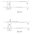
- FIG. 1there is illustrated a block diagram of a chalcogenide memory device in which a preferred embodiment of the present invention is incorporated.
- a memory matrix 11is formed on a substrate 10 .
- an addressing matrix 12is suitably connected to memory matrix 11 through connections 13 .
- Addressing matrix 12preferably includes various signal generating means that control and read pulses applied to memory matrix 11 .
- memory matrix 11includes an x-y grid with each of memory cells 20 being connected in series with an access device 21 at the cross points of x address lines 22 and y address lines 23 .
- Access device 21can be a diode or a transistor.
- Address lines 22 and 23are separately connected to external addressing circuitry, such as addressing matrix 12 from FIG. 1, in a manner that is well-known in the art.
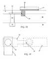
- FIGS. 3 a - 3 gare pictorial representations of a process for making a sidewall contact to be used in the chalcogenide memory device from FIG. 1, in accordance with a preferred embodiment of the present invention.
- a diffusion 31is first formed within a substrate 30 using well-known masking and doping techniques.
- Substrate 30may be silicon, gallium arsenide (GaAs), silicon molybdenum (SiMo) or any wafer material.
- a dielectric layer 32is deposited on top of substrate 30 .
- Dielectric layer 32may be silicon dioxide (SiO 2 ) or silicon nitride (SiN 2 ).
- a conventional contact (or via) 33is formed, using well-known masking and etching techniques, within dielectric layer 32 .
- the material sputtered inside contact 33is preferably tungsten (W). With the current technology, the size of contact 33 is preferably around 0.25 um in diameter.
- Bottom electrode layer 34is deposited on top of dielectric layer 32 , as shown in FIG. 3 b , using well-known masking and depositing techniques.
- Bottom electrode layer 34can be a metal layer such as titanium-aluminum nitride (TiAlN) or a polysilicon layer.
- TiAlNtitanium-aluminum nitride
- bottom electrode layer 34extends from contact 33 to a location at which a sidewall contact will be built.
- the cross-sectional dimension (i.e., width and thickness) of bottom electrode layer 34dictates the size of the contact area of the to-be built sidewall contact.
- bottom electrode layer 34is approximately 300 ⁇ thick.
- a dielectric layer 35which may be made of the same material as dielectric layer 32 , is deposited on top of bottom electrode layer 34 and dielectric layer 32 , as shown in FIG. 3 c .
- a opening 36is formed near one end of bottom electrode layer 34 within dielectric layer 32 , using well-known masking and etching techniques.
- the diameter of opening 36may be the same or larger than the diameter of contact 33 . With the current technology, the size of opening 36 is preferably around 0.25 um in diameter.
- etching processis use to etch the “exposed” portion of bottom electrode layer 34 within opening 36 to form a sidewall contact 39 , as shown in FIG. 3 d .
- a metal etch having high directional etch componentis preferably used to reduce undercutting of bottom electrode into the sidewall of opening 36 .
- the size of sidewall contact 39is the cross-sectional dimension of bottom electrode layer 34 .
- opening 36may be optionally etched deeper than dielectric layer 35 (i.e., deeper bottom electrode layer 34 ), as shown in FIG. 3 d.
- a chalcogenide layer 37is then deposited on top of bottom dielectric layer 34 , as shown in FIG. 3 e , using well-known masking and depositing techniques.
- chalcogenide layer 37is approximately 500 ⁇ thick.
- the sidewall of opening 36is covered with chalcogenide.
- sidewall contact 39is also covered with chalcogenide.
- Conventional masking and depositing techniquescan be used to deposit chalcogenide into opening 36 because the relatively large diameter of opening 36 does not pose any step coverage problem as compared to a relatively small opening. Thus, greater adhesion is made between sidewall contact 39 and chalcogenide layer 37 .
- FIG. 3 fA top view of FIG. 3 e is depicted in FIG. 3 f . As shown, sidewall contact 39 is in touch with the chalcogenide material within opening 36 . Consequently, bottom electrode layer 34 is in electrical connection with chalcogenide layer 37 .
- top electrode layer 38is deposited and patterned on top of chalcogenide layer 37 , as shown in FIG. 3 g using well-known masking and depositing techniques.
- Top electrode layer 38can be a metal layer or a polysilicon layer.
- dielectric layer 40is deposited on top of top electrode layer 38 and dielectric layer 35 .
- Dielectric layer 40may or may not be made of the same material as dielectric layers 32 and 35 .
- FIG. 4there is depicted a high-level process flow diagram of a method for manufacturing the sidewall contact from FIGS. 3 a - 3 g , in accordance with a preferred embodiment of the present invention.
- a first contactis formed within a first oxide layer on a substrate, as shown in block 42 .
- the first contactis for contacting a diffusion contained within the substrate.
- a first conductive layeris deposited and patterned on top of the first oxide layer, as depicted in block 43 .
- a second oxide layeris deposited on top of the first conductive layer and the first oxide layer, as shown in block 44 .
- An openingis then etched within the second oxide layer such that a portion of the first conductive layer is exposed within the opening, as depicted in block 45 .
- the exposed portion of the first conductive layeris removed from the opening by a well-known etching process such that the first conductive layer is flush with an inner surface (or sidewall) of the opening to form a sidewall contact, as shown in block 46 .
- a second conductive layeris deposited and patterned on top of the chalcogenide layer, as shown in block 48 .
- the present inventionprovides an improved method for manufacturing sidewall contacts for a chalcogenide memory device.
Landscapes
- Engineering & Computer Science (AREA)
- Manufacturing & Machinery (AREA)
- Physics & Mathematics (AREA)
- Condensed Matter Physics & Semiconductors (AREA)
- General Physics & Mathematics (AREA)
- Computer Hardware Design (AREA)
- Microelectronics & Electronic Packaging (AREA)
- Power Engineering (AREA)
- Semiconductor Memories (AREA)
Abstract
Description
Claims (10)
Priority Applications (2)
| Application Number | Priority Date | Filing Date | Title |
|---|---|---|---|
| US10/331,850US6815266B2 (en) | 2002-12-30 | 2002-12-30 | Method for manufacturing sidewall contacts for a chalcogenide memory device |
| US10/831,785US6909107B2 (en) | 2002-12-30 | 2004-04-26 | Method for manufacturing sidewall contacts for a chalcogenide memory device |
Applications Claiming Priority (1)
| Application Number | Priority Date | Filing Date | Title |
|---|---|---|---|
| US10/331,850US6815266B2 (en) | 2002-12-30 | 2002-12-30 | Method for manufacturing sidewall contacts for a chalcogenide memory device |
Related Child Applications (1)
| Application Number | Title | Priority Date | Filing Date |
|---|---|---|---|
| US10/831,785DivisionUS6909107B2 (en) | 2002-12-30 | 2004-04-26 | Method for manufacturing sidewall contacts for a chalcogenide memory device |
Publications (2)
| Publication Number | Publication Date |
|---|---|
| US20040126925A1 US20040126925A1 (en) | 2004-07-01 |
| US6815266B2true US6815266B2 (en) | 2004-11-09 |
Family
ID=32393157
Family Applications (2)
| Application Number | Title | Priority Date | Filing Date |
|---|---|---|---|
| US10/331,850Expired - LifetimeUS6815266B2 (en) | 2002-12-30 | 2002-12-30 | Method for manufacturing sidewall contacts for a chalcogenide memory device |
| US10/831,785Expired - LifetimeUS6909107B2 (en) | 2002-12-30 | 2004-04-26 | Method for manufacturing sidewall contacts for a chalcogenide memory device |
Family Applications After (1)
| Application Number | Title | Priority Date | Filing Date |
|---|---|---|---|
| US10/831,785Expired - LifetimeUS6909107B2 (en) | 2002-12-30 | 2004-04-26 | Method for manufacturing sidewall contacts for a chalcogenide memory device |
Country Status (1)
| Country | Link |
|---|---|
| US (2) | US6815266B2 (en) |
Cited By (8)
| Publication number | Priority date | Publication date | Assignee | Title |
|---|---|---|---|---|
| US20040166604A1 (en)* | 2003-02-25 | 2004-08-26 | Samsung Electronics Co. Ltd. | Phase changeable memory cells and methods of fabricating the same |
| US20050056937A1 (en)* | 2003-09-15 | 2005-03-17 | International Business Machines Corporation | Connection device and method of forming a connection device |
| US20060148125A1 (en)* | 2003-03-21 | 2006-07-06 | Hideki Horii | Phase changable memory device structures |
| US20080073638A1 (en)* | 2006-08-25 | 2008-03-27 | Micron Technology, Inc. | Programmable resistance memory devices and systems using the same and methods of forming the same |
| US20090189142A1 (en)* | 2008-01-25 | 2009-07-30 | Industrial Technology Research Institute | Phase-Change Memory |
| US20100006814A1 (en)* | 2008-07-11 | 2010-01-14 | Industrial Technology Research Institute | Phase-change memory element |
| US20100117050A1 (en)* | 2008-11-12 | 2010-05-13 | Industrial Technology Research Institute | Phase-change memory element |
| US8227785B2 (en)* | 2010-11-11 | 2012-07-24 | Micron Technology, Inc. | Chalcogenide containing semiconductors with chalcogenide gradient |
Families Citing this family (144)
| Publication number | Priority date | Publication date | Assignee | Title |
|---|---|---|---|---|
| US7319057B2 (en)* | 2001-10-30 | 2008-01-15 | Ovonyx, Inc. | Phase change material memory device |
| US6864503B2 (en)* | 2002-08-09 | 2005-03-08 | Macronix International Co., Ltd. | Spacer chalcogenide memory method and device |
| EP1439583B1 (en)* | 2003-01-15 | 2013-04-10 | STMicroelectronics Srl | Sublithographic contact structure, in particular for a phase change memory cell, and fabrication process thereof |
| US7067865B2 (en)* | 2003-06-06 | 2006-06-27 | Macronix International Co., Ltd. | High density chalcogenide memory cells |
| US20050184282A1 (en)* | 2004-02-20 | 2005-08-25 | Li-Shyue Lai | Phase change memory cell and method of its manufacture |
| US7608503B2 (en)* | 2004-11-22 | 2009-10-27 | Macronix International Co., Ltd. | Side wall active pin memory and manufacturing method |
| US7220983B2 (en)* | 2004-12-09 | 2007-05-22 | Macronix International Co., Ltd. | Self-aligned small contact phase-change memory method and device |
| US20080277642A1 (en)* | 2005-01-25 | 2008-11-13 | Nxp B.V. | Fabrication of Phase-Change Resistor Using a Backend Process |
| US8653495B2 (en)* | 2005-04-11 | 2014-02-18 | Micron Technology, Inc. | Heating phase change material |
| US7696503B2 (en) | 2005-06-17 | 2010-04-13 | Macronix International Co., Ltd. | Multi-level memory cell having phase change element and asymmetrical thermal boundary |
| US7598512B2 (en)* | 2005-06-17 | 2009-10-06 | Macronix International Co., Ltd. | Thin film fuse phase change cell with thermal isolation layer and manufacturing method |
| US7238994B2 (en)* | 2005-06-17 | 2007-07-03 | Macronix International Co., Ltd. | Thin film plate phase change ram circuit and manufacturing method |
| US7321130B2 (en)* | 2005-06-17 | 2008-01-22 | Macronix International Co., Ltd. | Thin film fuse phase change RAM and manufacturing method |
| US7534647B2 (en) | 2005-06-17 | 2009-05-19 | Macronix International Co., Ltd. | Damascene phase change RAM and manufacturing method |
| US7504652B2 (en)* | 2005-07-13 | 2009-03-17 | Taiwan Semiconductor Manufacturing Company, Ltd. | Phase change random access memory |
| US7394088B2 (en) | 2005-11-15 | 2008-07-01 | Macronix International Co., Ltd. | Thermally contained/insulated phase change memory device and method (combined) |
| US7450411B2 (en) | 2005-11-15 | 2008-11-11 | Macronix International Co., Ltd. | Phase change memory device and manufacturing method |
| US7635855B2 (en) | 2005-11-15 | 2009-12-22 | Macronix International Co., Ltd. | I-shaped phase change memory cell |
| US7786460B2 (en)* | 2005-11-15 | 2010-08-31 | Macronix International Co., Ltd. | Phase change memory device and manufacturing method |
| US7414258B2 (en) | 2005-11-16 | 2008-08-19 | Macronix International Co., Ltd. | Spacer electrode small pin phase change memory RAM and manufacturing method |
| US7449710B2 (en) | 2005-11-21 | 2008-11-11 | Macronix International Co., Ltd. | Vacuum jacket for phase change memory element |
| US7829876B2 (en) | 2005-11-21 | 2010-11-09 | Macronix International Co., Ltd. | Vacuum cell thermal isolation for a phase change memory device |
| US7507986B2 (en)* | 2005-11-21 | 2009-03-24 | Macronix International Co., Ltd. | Thermal isolation for an active-sidewall phase change memory cell |
| US7479649B2 (en)* | 2005-11-21 | 2009-01-20 | Macronix International Co., Ltd. | Vacuum jacketed electrode for phase change memory element |
| CN100524878C (en)* | 2005-11-21 | 2009-08-05 | 旺宏电子股份有限公司 | Programmable resistive material memory array with air-insulated cells |
| US7599217B2 (en)* | 2005-11-22 | 2009-10-06 | Macronix International Co., Ltd. | Memory cell device and manufacturing method |
| US7459717B2 (en) | 2005-11-28 | 2008-12-02 | Macronix International Co., Ltd. | Phase change memory cell and manufacturing method |
| US7688619B2 (en) | 2005-11-28 | 2010-03-30 | Macronix International Co., Ltd. | Phase change memory cell and manufacturing method |
| US7521364B2 (en)* | 2005-12-02 | 2009-04-21 | Macronix Internation Co., Ltd. | Surface topology improvement method for plug surface areas |
| US7531825B2 (en) | 2005-12-27 | 2009-05-12 | Macronix International Co., Ltd. | Method for forming self-aligned thermal isolation cell for a variable resistance memory array |
| US8062833B2 (en) | 2005-12-30 | 2011-11-22 | Macronix International Co., Ltd. | Chalcogenide layer etching method |
| US7595218B2 (en)* | 2006-01-09 | 2009-09-29 | Macronix International Co., Ltd. | Programmable resistive RAM and manufacturing method |
| US20070158632A1 (en)* | 2006-01-09 | 2007-07-12 | Macronix International Co., Ltd. | Method for Fabricating a Pillar-Shaped Phase Change Memory Element |
| US7741636B2 (en)* | 2006-01-09 | 2010-06-22 | Macronix International Co., Ltd. | Programmable resistive RAM and manufacturing method |
| US7560337B2 (en)* | 2006-01-09 | 2009-07-14 | Macronix International Co., Ltd. | Programmable resistive RAM and manufacturing method |
| US7432206B2 (en) | 2006-01-24 | 2008-10-07 | Macronix International Co., Ltd. | Self-aligned manufacturing method, and manufacturing method for thin film fuse phase change ram |
| US7956358B2 (en) | 2006-02-07 | 2011-06-07 | Macronix International Co., Ltd. | I-shaped phase change memory cell with thermal isolation |
| US7554144B2 (en) | 2006-04-17 | 2009-06-30 | Macronix International Co., Ltd. | Memory device and manufacturing method |
| US7928421B2 (en)* | 2006-04-21 | 2011-04-19 | Macronix International Co., Ltd. | Phase change memory cell with vacuum spacer |
| US7423300B2 (en)* | 2006-05-24 | 2008-09-09 | Macronix International Co., Ltd. | Single-mask phase change memory element |
| US7696506B2 (en) | 2006-06-27 | 2010-04-13 | Macronix International Co., Ltd. | Memory cell with memory material insulation and manufacturing method |
| US7785920B2 (en)* | 2006-07-12 | 2010-08-31 | Macronix International Co., Ltd. | Method for making a pillar-type phase change memory element |
| US7442603B2 (en)* | 2006-08-16 | 2008-10-28 | Macronix International Co., Ltd. | Self-aligned structure and method for confining a melting point in a resistor random access memory |
| JP4257352B2 (en)* | 2006-08-22 | 2009-04-22 | エルピーダメモリ株式会社 | Semiconductor memory device and manufacturing method of semiconductor memory device |
| US7772581B2 (en)* | 2006-09-11 | 2010-08-10 | Macronix International Co., Ltd. | Memory device having wide area phase change element and small electrode contact area |
| US7504653B2 (en)* | 2006-10-04 | 2009-03-17 | Macronix International Co., Ltd. | Memory cell device with circumferentially-extending memory element |
| US7510929B2 (en)* | 2006-10-18 | 2009-03-31 | Macronix International Co., Ltd. | Method for making memory cell device |
| US7388771B2 (en) | 2006-10-24 | 2008-06-17 | Macronix International Co., Ltd. | Methods of operating a bistable resistance random access memory with multiple memory layers and multilevel memory states |
| US7527985B2 (en)* | 2006-10-24 | 2009-05-05 | Macronix International Co., Ltd. | Method for manufacturing a resistor random access memory with reduced active area and reduced contact areas |
| US20080094885A1 (en)* | 2006-10-24 | 2008-04-24 | Macronix International Co., Ltd. | Bistable Resistance Random Access Memory Structures with Multiple Memory Layers and Multilevel Memory States |
| US7863655B2 (en) | 2006-10-24 | 2011-01-04 | Macronix International Co., Ltd. | Phase change memory cells with dual access devices |
| US8067762B2 (en)* | 2006-11-16 | 2011-11-29 | Macronix International Co., Ltd. | Resistance random access memory structure for enhanced retention |
| US7682868B2 (en) | 2006-12-06 | 2010-03-23 | Macronix International Co., Ltd. | Method for making a keyhole opening during the manufacture of a memory cell |
| US7476587B2 (en)* | 2006-12-06 | 2009-01-13 | Macronix International Co., Ltd. | Method for making a self-converged memory material element for memory cell |
| US20080137400A1 (en)* | 2006-12-06 | 2008-06-12 | Macronix International Co., Ltd. | Phase Change Memory Cell with Thermal Barrier and Method for Fabricating the Same |
| US7473576B2 (en)* | 2006-12-06 | 2009-01-06 | Macronix International Co., Ltd. | Method for making a self-converged void and bottom electrode for memory cell |
| US7697316B2 (en)* | 2006-12-07 | 2010-04-13 | Macronix International Co., Ltd. | Multi-level cell resistance random access memory with metal oxides |
| US7903447B2 (en)* | 2006-12-13 | 2011-03-08 | Macronix International Co., Ltd. | Method, apparatus and computer program product for read before programming process on programmable resistive memory cell |
| US8344347B2 (en)* | 2006-12-15 | 2013-01-01 | Macronix International Co., Ltd. | Multi-layer electrode structure |
| US7718989B2 (en)* | 2006-12-28 | 2010-05-18 | Macronix International Co., Ltd. | Resistor random access memory cell device |
| US7515461B2 (en)* | 2007-01-05 | 2009-04-07 | Macronix International Co., Ltd. | Current compliant sensing architecture for multilevel phase change memory |
| US7433226B2 (en)* | 2007-01-09 | 2008-10-07 | Macronix International Co., Ltd. | Method, apparatus and computer program product for read before programming process on multiple programmable resistive memory cell |
| US7440315B2 (en) | 2007-01-09 | 2008-10-21 | Macronix International Co., Ltd. | Method, apparatus and computer program product for stepped reset programming process on programmable resistive memory cell |
| US7663135B2 (en) | 2007-01-31 | 2010-02-16 | Macronix International Co., Ltd. | Memory cell having a side electrode contact |
| US7535756B2 (en) | 2007-01-31 | 2009-05-19 | Macronix International Co., Ltd. | Method to tighten set distribution for PCRAM |
| US7619311B2 (en) | 2007-02-02 | 2009-11-17 | Macronix International Co., Ltd. | Memory cell device with coplanar electrode surface and method |
| US7701759B2 (en)* | 2007-02-05 | 2010-04-20 | Macronix International Co., Ltd. | Memory cell device and programming methods |
| US7483292B2 (en)* | 2007-02-07 | 2009-01-27 | Macronix International Co., Ltd. | Memory cell with separate read and program paths |
| US7463512B2 (en)* | 2007-02-08 | 2008-12-09 | Macronix International Co., Ltd. | Memory element with reduced-current phase change element |
| US8138028B2 (en)* | 2007-02-12 | 2012-03-20 | Macronix International Co., Ltd | Method for manufacturing a phase change memory device with pillar bottom electrode |
| US7884343B2 (en)* | 2007-02-14 | 2011-02-08 | Macronix International Co., Ltd. | Phase change memory cell with filled sidewall memory element and method for fabricating the same |
| US8008643B2 (en)* | 2007-02-21 | 2011-08-30 | Macronix International Co., Ltd. | Phase change memory cell with heater and method for fabricating the same |
| US7619237B2 (en)* | 2007-02-21 | 2009-11-17 | Macronix International Co., Ltd. | Programmable resistive memory cell with self-forming gap |
| US7956344B2 (en)* | 2007-02-27 | 2011-06-07 | Macronix International Co., Ltd. | Memory cell with memory element contacting ring-shaped upper end of bottom electrode |
| US7786461B2 (en) | 2007-04-03 | 2010-08-31 | Macronix International Co., Ltd. | Memory structure with reduced-size memory element between memory material portions |
| US8610098B2 (en)* | 2007-04-06 | 2013-12-17 | Macronix International Co., Ltd. | Phase change memory bridge cell with diode isolation device |
| US7569844B2 (en) | 2007-04-17 | 2009-08-04 | Macronix International Co., Ltd. | Memory cell sidewall contacting side electrode |
| US7755076B2 (en)* | 2007-04-17 | 2010-07-13 | Macronix International Co., Ltd. | 4F2 self align side wall active phase change memory |
| US7483316B2 (en)* | 2007-04-24 | 2009-01-27 | Macronix International Co., Ltd. | Method and apparatus for refreshing programmable resistive memory |
| US8513637B2 (en)* | 2007-07-13 | 2013-08-20 | Macronix International Co., Ltd. | 4F2 self align fin bottom electrodes FET drive phase change memory |
| US7777215B2 (en) | 2007-07-20 | 2010-08-17 | Macronix International Co., Ltd. | Resistive memory structure with buffer layer |
| US7884342B2 (en)* | 2007-07-31 | 2011-02-08 | Macronix International Co., Ltd. | Phase change memory bridge cell |
| US7729161B2 (en) | 2007-08-02 | 2010-06-01 | Macronix International Co., Ltd. | Phase change memory with dual word lines and source lines and method of operating same |
| US9018615B2 (en)* | 2007-08-03 | 2015-04-28 | Macronix International Co., Ltd. | Resistor random access memory structure having a defined small area of electrical contact |
| US8178386B2 (en)* | 2007-09-14 | 2012-05-15 | Macronix International Co., Ltd. | Phase change memory cell array with self-converged bottom electrode and method for manufacturing |
| US7642125B2 (en)* | 2007-09-14 | 2010-01-05 | Macronix International Co., Ltd. | Phase change memory cell in via array with self-aligned, self-converged bottom electrode and method for manufacturing |
| US7551473B2 (en)* | 2007-10-12 | 2009-06-23 | Macronix International Co., Ltd. | Programmable resistive memory with diode structure |
| US7919766B2 (en) | 2007-10-22 | 2011-04-05 | Macronix International Co., Ltd. | Method for making self aligning pillar memory cell device |
| US7804083B2 (en)* | 2007-11-14 | 2010-09-28 | Macronix International Co., Ltd. | Phase change memory cell including a thermal protect bottom electrode and manufacturing methods |
| US7646631B2 (en)* | 2007-12-07 | 2010-01-12 | Macronix International Co., Ltd. | Phase change memory cell having interface structures with essentially equal thermal impedances and manufacturing methods |
| US7639527B2 (en) | 2008-01-07 | 2009-12-29 | Macronix International Co., Ltd. | Phase change memory dynamic resistance test and manufacturing methods |
| US7879643B2 (en)* | 2008-01-18 | 2011-02-01 | Macronix International Co., Ltd. | Memory cell with memory element contacting an inverted T-shaped bottom electrode |
| US7879645B2 (en) | 2008-01-28 | 2011-02-01 | Macronix International Co., Ltd. | Fill-in etching free pore device |
| US8158965B2 (en) | 2008-02-05 | 2012-04-17 | Macronix International Co., Ltd. | Heating center PCRAM structure and methods for making |
| US8084842B2 (en) | 2008-03-25 | 2011-12-27 | Macronix International Co., Ltd. | Thermally stabilized electrode structure |
| US8030634B2 (en) | 2008-03-31 | 2011-10-04 | Macronix International Co., Ltd. | Memory array with diode driver and method for fabricating the same |
| US7825398B2 (en) | 2008-04-07 | 2010-11-02 | Macronix International Co., Ltd. | Memory cell having improved mechanical stability |
| US7791057B2 (en) | 2008-04-22 | 2010-09-07 | Macronix International Co., Ltd. | Memory cell having a buried phase change region and method for fabricating the same |
| US8077505B2 (en) | 2008-05-07 | 2011-12-13 | Macronix International Co., Ltd. | Bipolar switching of phase change device |
| US7701750B2 (en) | 2008-05-08 | 2010-04-20 | Macronix International Co., Ltd. | Phase change device having two or more substantial amorphous regions in high resistance state |
| US7825397B2 (en)* | 2008-05-23 | 2010-11-02 | Seagate Technology Llc | Short bridge phase change memory cells |
| US8415651B2 (en) | 2008-06-12 | 2013-04-09 | Macronix International Co., Ltd. | Phase change memory cell having top and bottom sidewall contacts |
| US8134857B2 (en) | 2008-06-27 | 2012-03-13 | Macronix International Co., Ltd. | Methods for high speed reading operation of phase change memory and device employing same |
| US7932506B2 (en) | 2008-07-22 | 2011-04-26 | Macronix International Co., Ltd. | Fully self-aligned pore-type memory cell having diode access device |
| US7903457B2 (en) | 2008-08-19 | 2011-03-08 | Macronix International Co., Ltd. | Multiple phase change materials in an integrated circuit for system on a chip application |
| US7719913B2 (en) | 2008-09-12 | 2010-05-18 | Macronix International Co., Ltd. | Sensing circuit for PCRAM applications |
| US8324605B2 (en) | 2008-10-02 | 2012-12-04 | Macronix International Co., Ltd. | Dielectric mesh isolated phase change structure for phase change memory |
| US7897954B2 (en)* | 2008-10-10 | 2011-03-01 | Macronix International Co., Ltd. | Dielectric-sandwiched pillar memory device |
| US8036014B2 (en) | 2008-11-06 | 2011-10-11 | Macronix International Co., Ltd. | Phase change memory program method without over-reset |
| US8907316B2 (en) | 2008-11-07 | 2014-12-09 | Macronix International Co., Ltd. | Memory cell access device having a pn-junction with polycrystalline and single crystal semiconductor regions |
| US8664689B2 (en) | 2008-11-07 | 2014-03-04 | Macronix International Co., Ltd. | Memory cell access device having a pn-junction with polycrystalline plug and single-crystal semiconductor regions |
| US7869270B2 (en) | 2008-12-29 | 2011-01-11 | Macronix International Co., Ltd. | Set algorithm for phase change memory cell |
| US8089137B2 (en) | 2009-01-07 | 2012-01-03 | Macronix International Co., Ltd. | Integrated circuit memory with single crystal silicon on silicide driver and manufacturing method |
| US8107283B2 (en) | 2009-01-12 | 2012-01-31 | Macronix International Co., Ltd. | Method for setting PCRAM devices |
| US8030635B2 (en) | 2009-01-13 | 2011-10-04 | Macronix International Co., Ltd. | Polysilicon plug bipolar transistor for phase change memory |
| US8064247B2 (en) | 2009-01-14 | 2011-11-22 | Macronix International Co., Ltd. | Rewritable memory device based on segregation/re-absorption |
| US8933536B2 (en) | 2009-01-22 | 2015-01-13 | Macronix International Co., Ltd. | Polysilicon pillar bipolar transistor with self-aligned memory element |
| US8084760B2 (en) | 2009-04-20 | 2011-12-27 | Macronix International Co., Ltd. | Ring-shaped electrode and manufacturing method for same |
| US8173987B2 (en) | 2009-04-27 | 2012-05-08 | Macronix International Co., Ltd. | Integrated circuit 3D phase change memory array and manufacturing method |
| US8097871B2 (en) | 2009-04-30 | 2012-01-17 | Macronix International Co., Ltd. | Low operational current phase change memory structures |
| US7933139B2 (en) | 2009-05-15 | 2011-04-26 | Macronix International Co., Ltd. | One-transistor, one-resistor, one-capacitor phase change memory |
| US7968876B2 (en) | 2009-05-22 | 2011-06-28 | Macronix International Co., Ltd. | Phase change memory cell having vertical channel access transistor |
| US8350316B2 (en) | 2009-05-22 | 2013-01-08 | Macronix International Co., Ltd. | Phase change memory cells having vertical channel access transistor and memory plane |
| US8809829B2 (en) | 2009-06-15 | 2014-08-19 | Macronix International Co., Ltd. | Phase change memory having stabilized microstructure and manufacturing method |
| US8406033B2 (en) | 2009-06-22 | 2013-03-26 | Macronix International Co., Ltd. | Memory device and method for sensing and fixing margin cells |
| US8363463B2 (en) | 2009-06-25 | 2013-01-29 | Macronix International Co., Ltd. | Phase change memory having one or more non-constant doping profiles |
| US8238149B2 (en) | 2009-06-25 | 2012-08-07 | Macronix International Co., Ltd. | Methods and apparatus for reducing defect bits in phase change memory |
| US8110822B2 (en) | 2009-07-15 | 2012-02-07 | Macronix International Co., Ltd. | Thermal protect PCRAM structure and methods for making |
| US8198619B2 (en) | 2009-07-15 | 2012-06-12 | Macronix International Co., Ltd. | Phase change memory cell structure |
| US7894254B2 (en) | 2009-07-15 | 2011-02-22 | Macronix International Co., Ltd. | Refresh circuitry for phase change memory |
| US8064248B2 (en) | 2009-09-17 | 2011-11-22 | Macronix International Co., Ltd. | 2T2R-1T1R mix mode phase change memory array |
| US8178387B2 (en) | 2009-10-23 | 2012-05-15 | Macronix International Co., Ltd. | Methods for reducing recrystallization time for a phase change material |
| US8729521B2 (en) | 2010-05-12 | 2014-05-20 | Macronix International Co., Ltd. | Self aligned fin-type programmable memory cell |
| US8310864B2 (en) | 2010-06-15 | 2012-11-13 | Macronix International Co., Ltd. | Self-aligned bit line under word line memory array |
| US8395935B2 (en) | 2010-10-06 | 2013-03-12 | Macronix International Co., Ltd. | Cross-point self-aligned reduced cell size phase change memory |
| US8497705B2 (en) | 2010-11-09 | 2013-07-30 | Macronix International Co., Ltd. | Phase change device for interconnection of programmable logic device |
| US8467238B2 (en) | 2010-11-15 | 2013-06-18 | Macronix International Co., Ltd. | Dynamic pulse operation for phase change memory |
| CN103022347B (en)* | 2011-09-27 | 2016-03-09 | 中芯国际集成电路制造(北京)有限公司 | Semiconductor device and manufacture method thereof |
| US8987700B2 (en) | 2011-12-02 | 2015-03-24 | Macronix International Co., Ltd. | Thermally confined electrode for programmable resistance memory |
| US9336879B2 (en) | 2014-01-24 | 2016-05-10 | Macronix International Co., Ltd. | Multiple phase change materials in an integrated circuit for system on a chip application |
| US9559113B2 (en) | 2014-05-01 | 2017-01-31 | Macronix International Co., Ltd. | SSL/GSL gate oxide in 3D vertical channel NAND |
| US9159412B1 (en) | 2014-07-15 | 2015-10-13 | Macronix International Co., Ltd. | Staggered write and verify for phase change memory |
| US9672906B2 (en) | 2015-06-19 | 2017-06-06 | Macronix International Co., Ltd. | Phase change memory with inter-granular switching |
| US11158788B2 (en)* | 2018-10-30 | 2021-10-26 | International Business Machines Corporation | Atomic layer deposition and physical vapor deposition bilayer for additive patterning |
Citations (11)
| Publication number | Priority date | Publication date | Assignee | Title |
|---|---|---|---|---|
| US4242698A (en) | 1977-11-02 | 1980-12-30 | Texas Instruments Incorporated | Maximum density interconnections for large scale integrated circuits |
| US5276290A (en) | 1991-06-24 | 1994-01-04 | Shipley Company Inc. | Electroplating process and composition |
| US5321211A (en) | 1992-04-30 | 1994-06-14 | Sgs-Thomson Microelectronics, Inc. | Integrated circuit via structure |
| US5408130A (en) | 1992-08-31 | 1995-04-18 | Motorola, Inc. | Interconnection structure for conductive layers |
| US5407864A (en) | 1992-07-24 | 1995-04-18 | Samsung Electronics Co., Ltd. | Process for mounting a semiconductor chip and depositing contacts into through holes of a circuit board and of an insulating interposer and onto the chip |
| US5528000A (en) | 1993-08-18 | 1996-06-18 | Shipley Company, L.L.C. | Electroplating process and composition |
| US5879955A (en) | 1995-06-07 | 1999-03-09 | Micron Technology, Inc. | Method for fabricating an array of ultra-small pores for chalcogenide memory cells |
| US6124192A (en) | 1999-09-27 | 2000-09-26 | Vanguard International Semicondutor Corporation | Method for fabricating ultra-small interconnections using simplified patterns and sidewall contact plugs |
| US6337266B1 (en)* | 1996-07-22 | 2002-01-08 | Micron Technology, Inc. | Small electrode for chalcogenide memories |
| US6340631B1 (en) | 2000-05-31 | 2002-01-22 | Taiwan Semiconductor Manufacturing Company, Ltd | Method for laying out wide metal lines with embedded contacts/vias |
| US6653193B2 (en)* | 2000-12-08 | 2003-11-25 | Micron Technology, Inc. | Resistance variable device |
Family Cites Families (14)
| Publication number | Priority date | Publication date | Assignee | Title |
|---|---|---|---|---|
| US5789277A (en)* | 1996-07-22 | 1998-08-04 | Micron Technology, Inc. | Method of making chalogenide memory device |
| US5814527A (en)* | 1996-07-22 | 1998-09-29 | Micron Technology, Inc. | Method of making small pores defined by a disposable internal spacer for use in chalcogenide memories |
| JP3583583B2 (en)* | 1997-07-08 | 2004-11-04 | 株式会社東芝 | Semiconductor device and manufacturing method thereof |
| JP4237344B2 (en)* | 1998-09-29 | 2009-03-11 | 株式会社東芝 | Semiconductor device and manufacturing method thereof |
| JP3785003B2 (en)* | 1999-09-20 | 2006-06-14 | 株式会社東芝 | Method for manufacturing nonvolatile semiconductor memory device |
| JP2001168306A (en)* | 1999-12-09 | 2001-06-22 | Toshiba Corp | Nonvolatile semiconductor memory device and method of manufacturing the same |
| US6440837B1 (en)* | 2000-07-14 | 2002-08-27 | Micron Technology, Inc. | Method of forming a contact structure in a semiconductor device |
| US6613604B2 (en)* | 2001-08-02 | 2003-09-02 | Ovonyx, Inc. | Method for making small pore for use in programmable resistance memory element |
| US6545903B1 (en)* | 2001-12-17 | 2003-04-08 | Texas Instruments Incorporated | Self-aligned resistive plugs for forming memory cell with phase change material |
| US6855975B2 (en)* | 2002-04-10 | 2005-02-15 | Micron Technology, Inc. | Thin film diode integrated with chalcogenide memory cell |
| US7018863B2 (en)* | 2002-08-22 | 2006-03-28 | Micron Technology, Inc. | Method of manufacture of a resistance variable memory cell |
| KR100469128B1 (en)* | 2002-11-07 | 2005-01-29 | 삼성전자주식회사 | Method of forming floating gate of non-volatile memory device having self-aligned shallow trench isolation |
| JP3936315B2 (en)* | 2003-07-04 | 2007-06-27 | 株式会社東芝 | Semiconductor memory device and manufacturing method thereof |
| US7396720B2 (en)* | 2004-07-27 | 2008-07-08 | Micron Technology, Inc. | High coupling memory cell |
- 2002
- 2002-12-30USUS10/331,850patent/US6815266B2/ennot_activeExpired - Lifetime
- 2004
- 2004-04-26USUS10/831,785patent/US6909107B2/ennot_activeExpired - Lifetime
Patent Citations (12)
| Publication number | Priority date | Publication date | Assignee | Title |
|---|---|---|---|---|
| US4242698A (en) | 1977-11-02 | 1980-12-30 | Texas Instruments Incorporated | Maximum density interconnections for large scale integrated circuits |
| US5276290A (en) | 1991-06-24 | 1994-01-04 | Shipley Company Inc. | Electroplating process and composition |
| US5321211A (en) | 1992-04-30 | 1994-06-14 | Sgs-Thomson Microelectronics, Inc. | Integrated circuit via structure |
| US5407864A (en) | 1992-07-24 | 1995-04-18 | Samsung Electronics Co., Ltd. | Process for mounting a semiconductor chip and depositing contacts into through holes of a circuit board and of an insulating interposer and onto the chip |
| US5408130A (en) | 1992-08-31 | 1995-04-18 | Motorola, Inc. | Interconnection structure for conductive layers |
| US5528000A (en) | 1993-08-18 | 1996-06-18 | Shipley Company, L.L.C. | Electroplating process and composition |
| US5879955A (en) | 1995-06-07 | 1999-03-09 | Micron Technology, Inc. | Method for fabricating an array of ultra-small pores for chalcogenide memory cells |
| US6002140A (en) | 1995-06-07 | 1999-12-14 | Micron Technology, Inc. | Method for fabricating an array of ultra-small pores for chalcogenide memory cells |
| US6337266B1 (en)* | 1996-07-22 | 2002-01-08 | Micron Technology, Inc. | Small electrode for chalcogenide memories |
| US6124192A (en) | 1999-09-27 | 2000-09-26 | Vanguard International Semicondutor Corporation | Method for fabricating ultra-small interconnections using simplified patterns and sidewall contact plugs |
| US6340631B1 (en) | 2000-05-31 | 2002-01-22 | Taiwan Semiconductor Manufacturing Company, Ltd | Method for laying out wide metal lines with embedded contacts/vias |
| US6653193B2 (en)* | 2000-12-08 | 2003-11-25 | Micron Technology, Inc. | Resistance variable device |
Cited By (33)
| Publication number | Priority date | Publication date | Assignee | Title |
|---|---|---|---|---|
| US20110108794A1 (en)* | 2003-02-25 | 2011-05-12 | Yongho Ha | Phase Changeable Memory Devices |
| US7323734B2 (en)* | 2003-02-25 | 2008-01-29 | Samsung Electronics Co., Ltd. | Phase changeable memory cells |
| US20050245030A1 (en)* | 2003-02-25 | 2005-11-03 | Samsung Electronics Co., Ltd. | Phase changeable memory cells and methods of fabricating the same |
| US7893417B2 (en) | 2003-02-25 | 2011-02-22 | Samsung Electronics Co., Ltd. | Phase changeable memory devices |
| US20080272359A1 (en)* | 2003-02-25 | 2008-11-06 | Samsung Electronics Co., Ltd. | Phase changeable memory cells |
| US7329579B2 (en)* | 2003-02-25 | 2008-02-12 | Samsung Electronics Co., Ltd. | Phase changeable memory cells and methods of fabricating the same |
| US20040166604A1 (en)* | 2003-02-25 | 2004-08-26 | Samsung Electronics Co. Ltd. | Phase changeable memory cells and methods of fabricating the same |
| US7397092B2 (en) | 2003-03-21 | 2008-07-08 | Samsung Electronics Co., Ltd. | Phase changable memory device structures |
| US20080272357A1 (en)* | 2003-03-21 | 2008-11-06 | Samsung Electronics Co., Ltd. | Phase Changeable Memory Device Structures |
| US20060148125A1 (en)* | 2003-03-21 | 2006-07-06 | Hideki Horii | Phase changable memory device structures |
| US7763878B2 (en) | 2003-03-21 | 2010-07-27 | Samsung Electronics Co., Ltd. | Phase changeable memory device structures |
| US7342301B2 (en)* | 2003-09-15 | 2008-03-11 | International Business Machines Corporation | Connection device with actuating element for changing a conductive state of a via |
| US20050056937A1 (en)* | 2003-09-15 | 2005-03-17 | International Business Machines Corporation | Connection device and method of forming a connection device |
| US20060214301A1 (en)* | 2003-09-15 | 2006-09-28 | Frank David J | Connection device |
| US7074707B2 (en)* | 2003-09-15 | 2006-07-11 | International Business Machines Corporation | Method of fabricating a connection device |
| US20100065806A1 (en)* | 2006-08-25 | 2010-03-18 | Jun Liu | Programmable resistance memory devices and systems using the same and methods of forming the same |
| US7638357B2 (en)* | 2006-08-25 | 2009-12-29 | Micron Technology, Inc. | Programmable resistance memory devices and systems using the same and methods of forming the same |
| US20080073638A1 (en)* | 2006-08-25 | 2008-03-27 | Micron Technology, Inc. | Programmable resistance memory devices and systems using the same and methods of forming the same |
| US7960813B2 (en) | 2006-08-25 | 2011-06-14 | Micron Technology, Inc. | Programmable resistance memory devices and systems using the same and methods of forming the same |
| US8426838B2 (en) | 2008-01-25 | 2013-04-23 | Higgs Opl. Capital Llc | Phase-change memory |
| US9087985B2 (en) | 2008-01-25 | 2015-07-21 | Higgs Opl.Capital Llc | Phase-change memory |
| US20090189142A1 (en)* | 2008-01-25 | 2009-07-30 | Industrial Technology Research Institute | Phase-Change Memory |
| US8716099B2 (en) | 2008-01-25 | 2014-05-06 | Higgs Opl. Capital Llc | Phase-change memory |
| TWI387056B (en)* | 2008-07-11 | 2013-02-21 | Higgs Opl Capital Llc | Phase change memory and method for fabricating the same |
| US20100006814A1 (en)* | 2008-07-11 | 2010-01-14 | Industrial Technology Research Institute | Phase-change memory element |
| US7919768B2 (en) | 2008-07-11 | 2011-04-05 | Industrial Technology Research Institute | Phase-change memory element |
| US8604457B2 (en) | 2008-11-12 | 2013-12-10 | Higgs Opl. Capital Llc | Phase-change memory element |
| US8884260B2 (en) | 2008-11-12 | 2014-11-11 | Higgs Opl. Capital Llc | Phase change memory element |
| US20100117050A1 (en)* | 2008-11-12 | 2010-05-13 | Industrial Technology Research Institute | Phase-change memory element |
| US9245924B2 (en) | 2008-11-12 | 2016-01-26 | Higgs Opl. Capital Llc | Phase change memory element |
| US9735352B2 (en) | 2008-11-12 | 2017-08-15 | Gula Consulting Limited Liability Company | Phase change memory element |
| US10573807B2 (en) | 2008-11-12 | 2020-02-25 | Gula Consulting Limited Liability Company | Phase change memory element |
| US8227785B2 (en)* | 2010-11-11 | 2012-07-24 | Micron Technology, Inc. | Chalcogenide containing semiconductors with chalcogenide gradient |
Also Published As
| Publication number | Publication date |
|---|---|
| US20040197976A1 (en) | 2004-10-07 |
| US20040126925A1 (en) | 2004-07-01 |
| US6909107B2 (en) | 2005-06-21 |
Similar Documents
| Publication | Publication Date | Title |
|---|---|---|
| US6815266B2 (en) | Method for manufacturing sidewall contacts for a chalcogenide memory device | |
| US6514788B2 (en) | Method for manufacturing contacts for a Chalcogenide memory device | |
| US8026505B2 (en) | Memory device | |
| US7888666B2 (en) | Common word line edge contact phase-change memory | |
| EP0946975B1 (en) | A device and method for fabricating a small area of contact between electrodes | |
| US7687881B2 (en) | Small electrode for phase change memories | |
| US8143612B2 (en) | Phase change memory cell in via array with self-aligned, self-converged bottom electrode and method for manufacturing | |
| US7371604B2 (en) | Method of forming a contact structure | |
| WO1998036446A9 (en) | A method for fabricating a small area of contact between electrodes | |
| US20050029627A1 (en) | Damascene conductive line for contacting an underlying memory element | |
| US7525176B2 (en) | Phase change memory cell design with adjusted seam location |
Legal Events
| Date | Code | Title | Description |
|---|---|---|---|
| FEPP | Fee payment procedure | Free format text:PAYOR NUMBER ASSIGNED (ORIGINAL EVENT CODE: ASPN); ENTITY STATUS OF PATENT OWNER: LARGE ENTITY | |
| AS | Assignment | Owner name:BAE SYSTEMS INFORMATION AND ELECTRONIC SYSTEMS INT Free format text:ASSIGNMENT OF ASSIGNORS INTEREST;ASSIGNOR:RODGERS, JOHN C.;REEL/FRAME:014252/0172 Effective date:20031203 | |
| AS | Assignment | Owner name:BAE SYSTEMS INFORMATION AND ELECTRONIC SYSTEMS INT Free format text:ASSIGNMENT OF ASSIGNORS INTEREST;ASSIGNOR:RODGERS, JOHN C.;REEL/FRAME:014719/0752 Effective date:20040610 Owner name:BAE SYSTEMS INFORMATION AND ELECTRONIC SYSTEMS INT Free format text:ASSIGNMENT OF ASSIGNORS INTEREST;ASSIGNOR:RODGERS, JOHN C.;REEL/FRAME:014719/0777 Effective date:20040610 Owner name:OVNYX, INC., IDAHO Free format text:ASSIGNMENT OF ASSIGNORS INTEREST;ASSIGNOR:MAIMON, JON D.;REEL/FRAME:014719/0801 Effective date:20040608 Owner name:OVONYX, INC., IDAHO Free format text:ASSIGNMENT OF ASSIGNORS INTEREST;ASSIGNOR:MAIMON, JON D.;REEL/FRAME:014719/0797 Effective date:20040608 | |
| STCF | Information on status: patent grant | Free format text:PATENTED CASE | |
| CC | Certificate of correction | ||
| FPAY | Fee payment | Year of fee payment:4 | |
| FPAY | Fee payment | Year of fee payment:8 | |
| AS | Assignment | Owner name:U.S. NAVY AS REPRESENTED BY THE SECRETARY OF THE N Free format text:CONFIRMATORY LICENSE;ASSIGNOR:BAE SYSTEMS;REEL/FRAME:029582/0476 Effective date:20050426 | |
| AS | Assignment | Owner name:CARLOW INNOVATIONS LLC, VIRGINIA Free format text:ASSIGNMENT OF ASSIGNORS INTEREST;ASSIGNOR:OVONYX, INC.;REEL/FRAME:037244/0954 Effective date:20150731 | |
| FPAY | Fee payment | Year of fee payment:12 | |
| AS | Assignment | Owner name:OVONYX MEMORY TECHNOLOGY, LLC, VIRGINIA Free format text:CHANGE OF NAME;ASSIGNOR:CARLOW INNOVATIONS, LLC;REEL/FRAME:039379/0077 Effective date:20160708 |