US6815241B2 - GaN structures having low dislocation density and methods of manufacture - Google Patents
GaN structures having low dislocation density and methods of manufactureDownload PDFInfo
- Publication number
- US6815241B2 US6815241B2US10/255,181US25518102AUS6815241B2US 6815241 B2US6815241 B2US 6815241B2US 25518102 AUS25518102 AUS 25518102AUS 6815241 B2US6815241 B2US 6815241B2
- Authority
- US
- United States
- Prior art keywords
- layer
- depositing
- group iii
- low temperature
- high temperature
- Prior art date
- Legal status (The legal status is an assumption and is not a legal conclusion. Google has not performed a legal analysis and makes no representation as to the accuracy of the status listed.)
- Expired - Lifetime, expires
Links
- 238000000034methodMethods0.000titleclaimsabstractdescription69
- 238000004519manufacturing processMethods0.000titleclaimsdescription16
- 239000000463materialSubstances0.000claimsabstractdescription44
- 239000000758substrateSubstances0.000claimsdescription43
- 238000000151depositionMethods0.000claimsdescription39
- 150000001875compoundsChemical class0.000claimsdescription11
- 238000001947vapour-phase growthMethods0.000claimsdescription10
- 239000002648laminated materialSubstances0.000claimsdescription4
- 239000004065semiconductorSubstances0.000abstractdescription38
- 229910002601GaNInorganic materials0.000description77
- 230000007547defectEffects0.000description8
- 150000004767nitridesChemical class0.000description7
- 229910052594sapphireInorganic materials0.000description7
- 239000010980sapphireSubstances0.000description7
- JMASRVWKEDWRBT-UHFFFAOYSA-NGallium nitrideChemical compound[Ga]#NJMASRVWKEDWRBT-UHFFFAOYSA-N0.000description6
- 229910002704AlGaNInorganic materials0.000description4
- 239000013078crystalSubstances0.000description4
- -1nitride compoundsChemical class0.000description4
- VYPSYNLAJGMNEJ-UHFFFAOYSA-Nsilicon dioxideInorganic materialsO=[Si]=OVYPSYNLAJGMNEJ-UHFFFAOYSA-N0.000description4
- 208000012868OvergrowthDiseases0.000description3
- 238000005253claddingMethods0.000description3
- 238000005516engineering processMethods0.000description3
- 238000005530etchingMethods0.000description3
- 235000012239silicon dioxideNutrition0.000description3
- 238000004581coalescenceMethods0.000description2
- 238000002248hydride vapour-phase epitaxyMethods0.000description2
- 238000001451molecular beam epitaxyMethods0.000description2
- 230000003287optical effectEffects0.000description2
- 238000001020plasma etchingMethods0.000description2
- 239000010453quartzSubstances0.000description2
- 238000004544sputter depositionMethods0.000description2
- 235000012431wafersNutrition0.000description2
- 229910001218Gallium arsenideInorganic materials0.000description1
- OAICVXFJPJFONN-UHFFFAOYSA-NPhosphorusChemical compound[P]OAICVXFJPJFONN-UHFFFAOYSA-N0.000description1
- 239000000853adhesiveSubstances0.000description1
- 230000001070adhesive effectEffects0.000description1
- 238000000137annealingMethods0.000description1
- 230000000903blocking effectEffects0.000description1
- 238000005229chemical vapour depositionMethods0.000description1
- 238000004140cleaningMethods0.000description1
- 229910052681coesiteInorganic materials0.000description1
- 238000004320controlled atmosphereMethods0.000description1
- 238000007796conventional methodMethods0.000description1
- 229910052906cristobaliteInorganic materials0.000description1
- 230000008021depositionEffects0.000description1
- 230000001627detrimental effectEffects0.000description1
- 239000010432diamondSubstances0.000description1
- 229910003460diamondInorganic materials0.000description1
- 238000001312dry etchingMethods0.000description1
- 230000000694effectsEffects0.000description1
- 239000002223garnetSubstances0.000description1
- 239000011521glassSubstances0.000description1
- 230000008595infiltrationEffects0.000description1
- 238000001764infiltrationMethods0.000description1
- 239000007788liquidSubstances0.000description1
- 229910052751metalInorganic materials0.000description1
- 239000002184metalSubstances0.000description1
- 238000012986modificationMethods0.000description1
- 230000004048modificationEffects0.000description1
- 230000001902propagating effectEffects0.000description1
- 238000000926separation methodMethods0.000description1
- 239000000377silicon dioxideSubstances0.000description1
- 229910052682stishoviteInorganic materials0.000description1
- 238000003860storageMethods0.000description1
- 229910052905tridymiteInorganic materials0.000description1
- 238000007740vapor depositionMethods0.000description1
Images


Classifications
- C—CHEMISTRY; METALLURGY
- C30—CRYSTAL GROWTH
- C30B—SINGLE-CRYSTAL GROWTH; UNIDIRECTIONAL SOLIDIFICATION OF EUTECTIC MATERIAL OR UNIDIRECTIONAL DEMIXING OF EUTECTOID MATERIAL; REFINING BY ZONE-MELTING OF MATERIAL; PRODUCTION OF A HOMOGENEOUS POLYCRYSTALLINE MATERIAL WITH DEFINED STRUCTURE; SINGLE CRYSTALS OR HOMOGENEOUS POLYCRYSTALLINE MATERIAL WITH DEFINED STRUCTURE; AFTER-TREATMENT OF SINGLE CRYSTALS OR A HOMOGENEOUS POLYCRYSTALLINE MATERIAL WITH DEFINED STRUCTURE; APPARATUS THEREFOR
- C30B25/00—Single-crystal growth by chemical reaction of reactive gases, e.g. chemical vapour-deposition growth
- C30B25/02—Epitaxial-layer growth
- B—PERFORMING OPERATIONS; TRANSPORTING
- B82—NANOTECHNOLOGY
- B82Y—SPECIFIC USES OR APPLICATIONS OF NANOSTRUCTURES; MEASUREMENT OR ANALYSIS OF NANOSTRUCTURES; MANUFACTURE OR TREATMENT OF NANOSTRUCTURES
- B82Y20/00—Nanooptics, e.g. quantum optics or photonic crystals
- C—CHEMISTRY; METALLURGY
- C30—CRYSTAL GROWTH
- C30B—SINGLE-CRYSTAL GROWTH; UNIDIRECTIONAL SOLIDIFICATION OF EUTECTIC MATERIAL OR UNIDIRECTIONAL DEMIXING OF EUTECTOID MATERIAL; REFINING BY ZONE-MELTING OF MATERIAL; PRODUCTION OF A HOMOGENEOUS POLYCRYSTALLINE MATERIAL WITH DEFINED STRUCTURE; SINGLE CRYSTALS OR HOMOGENEOUS POLYCRYSTALLINE MATERIAL WITH DEFINED STRUCTURE; AFTER-TREATMENT OF SINGLE CRYSTALS OR A HOMOGENEOUS POLYCRYSTALLINE MATERIAL WITH DEFINED STRUCTURE; APPARATUS THEREFOR
- C30B29/00—Single crystals or homogeneous polycrystalline material with defined structure characterised by the material or by their shape
- C30B29/10—Inorganic compounds or compositions
- C30B29/40—AIIIBV compounds wherein A is B, Al, Ga, In or Tl and B is N, P, As, Sb or Bi
- H—ELECTRICITY
- H01—ELECTRIC ELEMENTS
- H01L—SEMICONDUCTOR DEVICES NOT COVERED BY CLASS H10
- H01L21/00—Processes or apparatus adapted for the manufacture or treatment of semiconductor or solid state devices or of parts thereof
- H01L21/02—Manufacture or treatment of semiconductor devices or of parts thereof
- H01L21/02104—Forming layers
- H01L21/02365—Forming inorganic semiconducting materials on a substrate
- H01L21/02367—Substrates
- H01L21/0237—Materials
- H01L21/02373—Group 14 semiconducting materials
- H01L21/02378—Silicon carbide
- H—ELECTRICITY
- H01—ELECTRIC ELEMENTS
- H01L—SEMICONDUCTOR DEVICES NOT COVERED BY CLASS H10
- H01L21/00—Processes or apparatus adapted for the manufacture or treatment of semiconductor or solid state devices or of parts thereof
- H01L21/02—Manufacture or treatment of semiconductor devices or of parts thereof
- H01L21/02104—Forming layers
- H01L21/02365—Forming inorganic semiconducting materials on a substrate
- H01L21/02367—Substrates
- H01L21/0237—Materials
- H01L21/0242—Crystalline insulating materials
- H—ELECTRICITY
- H01—ELECTRIC ELEMENTS
- H01L—SEMICONDUCTOR DEVICES NOT COVERED BY CLASS H10
- H01L21/00—Processes or apparatus adapted for the manufacture or treatment of semiconductor or solid state devices or of parts thereof
- H01L21/02—Manufacture or treatment of semiconductor devices or of parts thereof
- H01L21/02104—Forming layers
- H01L21/02365—Forming inorganic semiconducting materials on a substrate
- H01L21/02436—Intermediate layers between substrates and deposited layers
- H01L21/02439—Materials
- H01L21/02455—Group 13/15 materials
- H01L21/02458—Nitrides
- H—ELECTRICITY
- H01—ELECTRIC ELEMENTS
- H01L—SEMICONDUCTOR DEVICES NOT COVERED BY CLASS H10
- H01L21/00—Processes or apparatus adapted for the manufacture or treatment of semiconductor or solid state devices or of parts thereof
- H01L21/02—Manufacture or treatment of semiconductor devices or of parts thereof
- H01L21/02104—Forming layers
- H01L21/02365—Forming inorganic semiconducting materials on a substrate
- H01L21/02436—Intermediate layers between substrates and deposited layers
- H01L21/02439—Materials
- H01L21/02469—Group 12/16 materials
- H01L21/02472—Oxides
- H—ELECTRICITY
- H01—ELECTRIC ELEMENTS
- H01L—SEMICONDUCTOR DEVICES NOT COVERED BY CLASS H10
- H01L21/00—Processes or apparatus adapted for the manufacture or treatment of semiconductor or solid state devices or of parts thereof
- H01L21/02—Manufacture or treatment of semiconductor devices or of parts thereof
- H01L21/02104—Forming layers
- H01L21/02365—Forming inorganic semiconducting materials on a substrate
- H01L21/02436—Intermediate layers between substrates and deposited layers
- H01L21/02494—Structure
- H01L21/02496—Layer structure
- H01L21/02502—Layer structure consisting of two layers
- H—ELECTRICITY
- H01—ELECTRIC ELEMENTS
- H01L—SEMICONDUCTOR DEVICES NOT COVERED BY CLASS H10
- H01L21/00—Processes or apparatus adapted for the manufacture or treatment of semiconductor or solid state devices or of parts thereof
- H01L21/02—Manufacture or treatment of semiconductor devices or of parts thereof
- H01L21/02104—Forming layers
- H01L21/02365—Forming inorganic semiconducting materials on a substrate
- H01L21/02518—Deposited layers
- H01L21/02521—Materials
- H01L21/02538—Group 13/15 materials
- H01L21/0254—Nitrides
- H—ELECTRICITY
- H01—ELECTRIC ELEMENTS
- H01L—SEMICONDUCTOR DEVICES NOT COVERED BY CLASS H10
- H01L21/00—Processes or apparatus adapted for the manufacture or treatment of semiconductor or solid state devices or of parts thereof
- H01L21/02—Manufacture or treatment of semiconductor devices or of parts thereof
- H01L21/02104—Forming layers
- H01L21/02365—Forming inorganic semiconducting materials on a substrate
- H01L21/02612—Formation types
- H01L21/02617—Deposition types
- H01L21/0262—Reduction or decomposition of gaseous compounds, e.g. CVD
- H—ELECTRICITY
- H01—ELECTRIC ELEMENTS
- H01L—SEMICONDUCTOR DEVICES NOT COVERED BY CLASS H10
- H01L21/00—Processes or apparatus adapted for the manufacture or treatment of semiconductor or solid state devices or of parts thereof
- H01L21/02—Manufacture or treatment of semiconductor devices or of parts thereof
- H01L21/02104—Forming layers
- H01L21/02365—Forming inorganic semiconducting materials on a substrate
- H01L21/02612—Formation types
- H01L21/02617—Deposition types
- H01L21/02636—Selective deposition, e.g. simultaneous growth of mono- and non-monocrystalline semiconductor materials
- H01L21/02639—Preparation of substrate for selective deposition
- H—ELECTRICITY
- H01—ELECTRIC ELEMENTS
- H01L—SEMICONDUCTOR DEVICES NOT COVERED BY CLASS H10
- H01L21/00—Processes or apparatus adapted for the manufacture or treatment of semiconductor or solid state devices or of parts thereof
- H01L21/02—Manufacture or treatment of semiconductor devices or of parts thereof
- H01L21/02104—Forming layers
- H01L21/02365—Forming inorganic semiconducting materials on a substrate
- H01L21/02612—Formation types
- H01L21/02617—Deposition types
- H01L21/02636—Selective deposition, e.g. simultaneous growth of mono- and non-monocrystalline semiconductor materials
- H01L21/02647—Lateral overgrowth
- H—ELECTRICITY
- H01—ELECTRIC ELEMENTS
- H01S—DEVICES USING THE PROCESS OF LIGHT AMPLIFICATION BY STIMULATED EMISSION OF RADIATION [LASER] TO AMPLIFY OR GENERATE LIGHT; DEVICES USING STIMULATED EMISSION OF ELECTROMAGNETIC RADIATION IN WAVE RANGES OTHER THAN OPTICAL
- H01S5/00—Semiconductor lasers
- H01S5/30—Structure or shape of the active region; Materials used for the active region
- H01S5/34—Structure or shape of the active region; Materials used for the active region comprising quantum well or superlattice structures, e.g. single quantum well [SQW] lasers, multiple quantum well [MQW] lasers or graded index separate confinement heterostructure [GRINSCH] lasers
- H01S5/343—Structure or shape of the active region; Materials used for the active region comprising quantum well or superlattice structures, e.g. single quantum well [SQW] lasers, multiple quantum well [MQW] lasers or graded index separate confinement heterostructure [GRINSCH] lasers in AIIIBV compounds, e.g. AlGaAs-laser, InP-based laser
- H01S5/34333—Structure or shape of the active region; Materials used for the active region comprising quantum well or superlattice structures, e.g. single quantum well [SQW] lasers, multiple quantum well [MQW] lasers or graded index separate confinement heterostructure [GRINSCH] lasers in AIIIBV compounds, e.g. AlGaAs-laser, InP-based laser with a well layer based on Ga(In)N or Ga(In)P, e.g. blue laser
- H—ELECTRICITY
- H10—SEMICONDUCTOR DEVICES; ELECTRIC SOLID-STATE DEVICES NOT OTHERWISE PROVIDED FOR
- H10H—INORGANIC LIGHT-EMITTING SEMICONDUCTOR DEVICES HAVING POTENTIAL BARRIERS
- H10H20/00—Individual inorganic light-emitting semiconductor devices having potential barriers, e.g. light-emitting diodes [LED]
- H10H20/01—Manufacture or treatment
- H10H20/011—Manufacture or treatment of bodies, e.g. forming semiconductor layers
- H10H20/013—Manufacture or treatment of bodies, e.g. forming semiconductor layers having light-emitting regions comprising only Group III-V materials
- H10H20/0133—Manufacture or treatment of bodies, e.g. forming semiconductor layers having light-emitting regions comprising only Group III-V materials with a substrate not being Group III-V materials
- H10H20/01335—Manufacture or treatment of bodies, e.g. forming semiconductor layers having light-emitting regions comprising only Group III-V materials with a substrate not being Group III-V materials the light-emitting regions comprising nitride materials
- H—ELECTRICITY
- H01—ELECTRIC ELEMENTS
- H01S—DEVICES USING THE PROCESS OF LIGHT AMPLIFICATION BY STIMULATED EMISSION OF RADIATION [LASER] TO AMPLIFY OR GENERATE LIGHT; DEVICES USING STIMULATED EMISSION OF ELECTROMAGNETIC RADIATION IN WAVE RANGES OTHER THAN OPTICAL
- H01S2304/00—Special growth methods for semiconductor lasers
- H01S2304/12—Pendeo epitaxial lateral overgrowth [ELOG], e.g. for growing GaN based blue laser diodes
- H—ELECTRICITY
- H01—ELECTRIC ELEMENTS
- H01S—DEVICES USING THE PROCESS OF LIGHT AMPLIFICATION BY STIMULATED EMISSION OF RADIATION [LASER] TO AMPLIFY OR GENERATE LIGHT; DEVICES USING STIMULATED EMISSION OF ELECTROMAGNETIC RADIATION IN WAVE RANGES OTHER THAN OPTICAL
- H01S5/00—Semiconductor lasers
- H01S5/02—Structural details or components not essential to laser action
- H01S5/0206—Substrates, e.g. growth, shape, material, removal or bonding
- H01S5/0213—Sapphire, quartz or diamond based substrates
- H—ELECTRICITY
- H01—ELECTRIC ELEMENTS
- H01S—DEVICES USING THE PROCESS OF LIGHT AMPLIFICATION BY STIMULATED EMISSION OF RADIATION [LASER] TO AMPLIFY OR GENERATE LIGHT; DEVICES USING STIMULATED EMISSION OF ELECTROMAGNETIC RADIATION IN WAVE RANGES OTHER THAN OPTICAL
- H01S5/00—Semiconductor lasers
- H01S5/02—Structural details or components not essential to laser action
- H01S5/0206—Substrates, e.g. growth, shape, material, removal or bonding
- H01S5/0218—Substrates comprising semiconducting materials from other groups of the Periodic Table than the materials of the active layer
- H—ELECTRICITY
- H01—ELECTRIC ELEMENTS
- H01S—DEVICES USING THE PROCESS OF LIGHT AMPLIFICATION BY STIMULATED EMISSION OF RADIATION [LASER] TO AMPLIFY OR GENERATE LIGHT; DEVICES USING STIMULATED EMISSION OF ELECTROMAGNETIC RADIATION IN WAVE RANGES OTHER THAN OPTICAL
- H01S5/00—Semiconductor lasers
- H01S5/20—Structure or shape of the semiconductor body to guide the optical wave ; Confining structures perpendicular to the optical axis, e.g. index or gain guiding, stripe geometry, broad area lasers, gain tailoring, transverse or lateral reflectors, special cladding structures, MQW barrier reflection layers
- H01S5/2004—Confining in the direction perpendicular to the layer structure
- H01S5/2009—Confining in the direction perpendicular to the layer structure by using electron barrier layers
Definitions
- the inventions disclosed hereinrelate to various GaN semiconductor devices, including those with a selective etching low-temperature buffer, and related methods for growing single crystal III-V compound semiconductor layers, including those where such layers include nitrides.
- GaN and its related semiconductorshave been used to produce UV, blue, green, red LEDs and UV and near UV lasers.
- the LEDs using GaN materialshave been widely used in large indoor/outdoor displays, traffic signals, local lighting and others.
- Lasers using GaN materialstend to have life spans on the order of hundreds of hours. It is desirable that such devices have a lifespan of about 10,000 or more hours to be practicable in consumer electronics.
- the short lifetime in GaN lasersis due to the increased defects in the initial GaN layer which results in defects being transported to light emitting layers.
- a usual GaN device structureconsists of multiple layers of different type of materials and is built using epitaxial methods. Each layer requires near perfect crystal structure. Since there is no lattice matched substrate materials available for GaN material, GaN materials has to be grown in lattice mismatch substrate such as sapphire, SiC and etc. Thus, initial GaN layer grown has high defect density caused by lattice mismatch. The defects generated in initial GaN growth will propagate into sequential layers resulting in high defect density in critical layers for devices. The defects in critical layers of the device are detrimental to lifetime. Thus there is a need for initial GaN layer in mismatched substrate having low densities of defects being producible through conventional and reasonably inexpensive methods.
- U.S. Pat. No. 5,563,422 and related U.S. Pat. Nos. 5,767,581; 5,877,558 and 6,093,965describe GaN based semiconductor devices, some of which are light producing.
- U.S. Pat. No. 5,578,839 and related U.S. Pat. Nos. 5,880,486 and 6,078,063also describe GaN light-emitting semiconductor devices.
- U.S. Pat. No. 5,689,123 and related U.S. Pat. No. 5,689,123describe III-V arsenide-nitride semiconductor devices.
- U.S. Pat. No. 5,739,554 and related U.S. Pat. No. 6,120,600describe light emitting diodes having a GaN active layer.
- U.S. Pat. No. 5,886,367describes a epitaxial wafer and a light emitting devices using the same.
- U.S. Pat. No. 5,987,048 and related U.S. Pat. No. 6,118,801describe GaN based semiconductor lasers.
- U.S. Pat. No. 5,945,689describes light emitting devices using group III nitride compounds.
- U.S. Pat. No. 5,970,080describes GaN light emitting elements and methods of manufacture.
- U.S. Pat. No. 6,005,258also describes GaN based light emitting semiconductor devices.
- U.S. Pat. No. 6,017,807describes P-type GaN semiconductor devices and methods of manufacture.
- U.S. Pat. No. 6,020,602also describes GaN based light emitting devices and methods of manufacture.
- U.S. Pat. No. 6,027,992describes GaN semiconductor devices and methods of manufacture.
- U.S. Pat. No. 6,028,887describes a GaN semiconductor laser having an AlGaN cladding layer.
- U.S. Pat. No. 6,033,490describes methods of growing GaN layers on quartz substrates.
- U.S. Pat. No. 6,051,849discloses structures having an underlying gallium nitride layer, a patterned layer, and a vertical and lateral gallium nitride layer having a low disclocation density.
- U.S. Pat. No. 6,067,309also describes a GaN light-emitting semiconductor device.
- U.S. Pat. No. 6,069,021describes semiconductor devices including group III nitride crystal layers and methods of manufacture.
- U.S. Pat. No. 6,069,440describes a nitride compound light emitting device having a garnet fluorescent phosphor.
- 6,072,189describes group III light-emitting diodes and laser diodes on a sapphire substrate.
- U.S. Pat. No. 6,078,064describes an InGaN light emitting diode.
- U.S. Pat. No. 6,091,083describes a GaN semiconductor light emitting device having a non-flat buffer layer.
- U.S. Pat. No. 6,093,952describes a high-power GaN schottky rectifier.
- U.S. Pat. No. 6,100,106describes processes of the manufacture of nitride based semiconductor light emitting devices.
- U.S. Pat. No. 6,110,809describes the manufacture of wafers with group III metal nitride epitaxial layers.
- 6,111,275describes GaN compound semiconductor light emitting devices and methods of manufacture.
- U.S. Pat. No. 6,111,277describes light emitting semiconductor devices having mask layers to prevent threading dislocations from propagating to successive semiconductor layers during manufacture.
- U.S. Pat. No. 6,113,985describes the manufacture of group III nitride targets for use in sputtering and similar equipment.
- U.S. Pat. No. 6,121,636describes a GaN light emitting diode having a reflective film to prevent the infiltration of light to mounting adhesive.
- U.S. Pat. No. 6,121,637describes a packaged light emitting semiconductor device. All of the above U.S. patents in their entirety are hereby incorporated by reference.
- Included in the inventionare laminates having layers of group III-V materials having low dislocation densities, semiconductor devices fabricated using low dislocation density group III-V layers, and methods for making these structures.
- the inventionsit is desired to provide methods for growing one or more group III-V compound semiconductor layers of nitrides having low dislocation densities on a substrate that has a large lattice mismatch compared with GaN and other group III-V compounds.
- Some of the inventionsare concerned with GaN layers, GaN semiconductor devices, and semiconductor lasers fabricated from GaN materials.
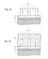
- FIGS. 1 a - 1 bdepict a method of creating a low dislocation density GaN layer on a substrate.
- FIGS. 2 a - 2 cdepict a method of creating a low dislocation density GaN layer on a substrate.
- FIGS. 3 a - 3 idepict an improved method of creating a GaN layer having areas of reduced dislocations on a substrate.
- FIG. 4depicts a semiconductor laser fabricated on a low dislocation area of a GaN layer on a lattice mismatch substrate.
- One first related method of creating GaN semiconductor layersuses a sapphire or SiC substrate and metalorganic chemical vapor deposition (MOCVD).
- MOCVDmetalorganic chemical vapor deposition
- Conventional methodsutilize a first annealing step in which the substrate is heated to a high temperature, 1000° C. or higher, in a controlled atmosphere, such as pure H2.
- a very thin buffer layer of GaN or AlN grown at a low temperaturefor example 400 to 600° C. for a sapphire substrate since the critical layer thickness to release the lattice mismatch between GaN (or AlN) and sapphire or SiC substrate to generate dislocations at low temperature will be thicker than higher growth temperature.
- the GaN layer grownis less than a critical thickness, the GaN layer will be relatively free of defects.
- a successive base layer of undoped GaNis grown at a high temperature, typically over 1000° C., to a specified thickness, for example 2 ⁇ m.
- Successive layers of doped GaN or other compatible materialsmay then be deposited on the base layer to form a semiconductor device. In practice this method yields layers of GaN with relatively high densities of dislocations.
- a laminateis produced following the procedure of the first method having a substrate 101 , a buffer layer 102 , a base layer 103 .
- a series of strips of SiO2, Si x N 1 ⁇ x , or other materialis deposited to the base layer in the GaN ⁇ 1 ⁇ overscore (1) ⁇ 00> direction forming a mask layer 104 , as shown in FIG. 1 a .
- the width of the strips compared to the separation between the strips 105is usually made to be 1:2.
- a new high temperature GaN layer 106is re-grown at a high temperature of more than 1000° C., first vertically and then laterally over the mask strips until the lateral growth fronts coalesce to form a continuous layer, as in FIG. 1 b .
- the material grown laterally over the mask stripsis the overgrowth region 107 .
- the growth of the high temperature GaN layeris generally thought to proceed by an islanding and coalescence mechanism.
- the initial growth of the high temperature GaN layerappears in the form of islands with a truncated hexagonal pyramid shape, the islands coalescing where they meet. After coalescence and further growth the layer eventually becomes flat.
- the dislocation density of the GaN layer in the overgrowth regionwill be greatly reduced, and can be used as a new high-quality substrate for producing successive GaN compound layers also having a reduced dislocation density.
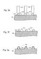
- a laminateis produced following the procedure of the first method having a substrate 201 , a buffer layer 202 , a base layer 203 .
- a patterned mask layeris applied 204 leaving apertures 205 , as shown in FIG. 2 a .
- the GaNis then selectively etched down to the substrate through apertures 205 leaving troughs 206 , as shown in FIG. 2 b .
- the pattern maskis then removed.
- the laminateis then introduced into a MOCVD apparatus for growth of a new high temperature GaN layer 207 , with overgrowth regions 208 having improved dislocation density, as shown in FIG. 2 c.
- GaNsuch as sapphire, sapphire/quartz, SiC, Si, GaAs, glass, diamond and others
- FIG. 3demonstrates steps of a method of the invention by showing a laminate material in cross-section at various stages of the method.
- the first step of the methodis to obtain a substrate 300 such as one of those listed above or another appropriate substrate, as shown in FIG. 3 a .
- a vapor phase deposition techniqueis used to grow a low temperature buffer layer 302 a on substrate 300 , as shown in FIG. 3 b .
- MOCVD, sputtering deposition, MBE (molecular beam epitaxy) and HVPE (hydride vapor phase epitaxy)are among suitable techniques for growing a low temperature buffer layer.
- the temperature for growing a low temperature buffer layer according to the inventionwill preferably be in the range of from about 200° C.
- the material for the low temperature buffer layermay include AlN, GaN, or ZnO and other suitable materials.
- An example of appropriate thickness for the low temperature buffer layeris about 10-50 nm, although low temperature buffer layers of greater or less thickness may also be constructed according to the inventive concepts.
- a pattern mask layer 304 ais deposited to the laminate, as shown in FIG. 3 c . Selected portions of the mask are removed leaving islands of mask 304 b with apertures 306 in between. In some methods the islands are strips, intended to produce strips of low temperature buffer material. Apertures 306 should generally run in the GaN ⁇ 1 ⁇ overscore (1) ⁇ 00> direction in order to achieve low dislocation densities.
- the mask layeris a photo-sensitive resist layer deposited in liquid form using spin-coat technology, and baked or cured to harden. This layer is typically at least several micrometers thick to provide structural strength. The photo-resist mask is then exposed to light through a photo mask having a predetermined pattern. The non-exposed portions of the photo-resist are then removed.
- the low-temperature buffer 302 ais selectively etched down in the direction of the substrate 300 , by which material from the low temperature buffer layer is removed.
- the resultis a number of low temperature buffer material islands 302 b separated by troughs 308 , as shown in FIG. 3 e .
- these islandsmay be features of a larger mass of low temperature buffer material, such as peninsulas, so long as they are separated by empty troughs.
- the walls of the islands 302 bmay not necessarily be perpendicular to the substrate, but may have a slope which is a side effect of many etchant processes.
- a dry etching technologysuch as ICP (intensed coupled plasma) and RIE (reactive ion etching) can be used for the etching step.
- ICPintensed coupled plasma
- RIEreactive ion etching
- the remaining mask 304 bis removed in a cleaning step, with the resulting structure of FIG. 3 f .
- the troughs 308there is preferably no appreciable low temperature buffer material.
- the ratio of the width of the low temperature buffer islands to the troughsmay be as desired, although it will be seen that a wider trough may produce proportionately more areas of low dislocation density material, but may also require longer successive growth periods.
- the substrate 300 with the above-described low temperature buffer islands 302 b and intervening troughs 306is next re-introduced into a vapor deposition growth chamber for re-growth of a vertically grown layer.
- the substrate temperatureis raised to a high temperature, preferably greater than 1000° C.
- GaNforms only on the low-temperature buffer strips 302 b but not on the substrate 300 in the troughs 306 .
- the aforementioned temperature and V/III ratio(the V/III ratio is from 50000 to 500) is considered optimal for the enhancement of vertical growth.
- a certain thickness of material 309is grown, preferably about 0.7 ⁇ m to about 1 ⁇ m, as shown in FIG. 3 g .
- the V/III ratiois changed (10000 to 100) for the enhancement of lateral growth.
- the growth of materialcontinues generally in the direction of the arrows. So called threading dislocations are continued in that direction of growth, leading to material which is relatively high in dislocations.
- the lateral growth fronts 310 originating from the low temperature buffer islandscoalesce at divisions 312 to form a continuous layer of GaN 314 .
- the growth of the GaN layeris allowed to continue until a desired thickness is achieved in accordance with flatness, structural, thermal, and other requirements.
- 3 ishows the resulting laminate with divisions 312 where growth fronts have met, regions having high dislocation density 316 , and regions of low dislocation density 318 .
- the surface of the resulting GaN layerincludes areas 320 with reduced dislocation density on which other III/V structures may be grown inheriting the low dislocation density of the underlying layer.
- the second growth temperaturecan be ranged from about 800 to about 130° C.
- V/III ratiocan be about 50,000 to about 100
- spacing between islandscan be ranged from about 10 to about 500 ⁇ m
- the layer thicknesscan be ranged from about 2 to about 100 ⁇ m.
- a substrate 401is provided.
- the substrate 401may be of any of the previously mentioned substrate materials or another suitable material.
- low temperature buffer strips 402 with intervening troughsare formed as already described.
- GaNis re-grown on the strips in a new layer 403 a , and that new layer eventually coalesces over the troughs to form a continuous and uninterrupted layer 403 b .
- Region 404provides a low dislocation density substrate for the remaining semiconductor layers.
- an n-type GaN contact layer 405from 1 to 5 ⁇ m in thickness is grown followed by a n-type AlGaN/GaN strain-layer supperlattice (SLS) 406 from 0.3 ⁇ m to 1.5 ⁇ m in thickness as a cladding layer. Then a 0.1 to 0.2 ⁇ m n-type GaN as a guiding layer 407 is deposited. Next, 1 to 10 periods of InGaN/GaN multiple-quantum-well structures, shown as five layers 408 a - 408 e , that are 0.01-0.02 ⁇ m in thickness are deposited. These layers 408 a - 408 e are the active layers from which light is produced.
- SLSn-type AlGaN/GaN strain-layer supperlattice
- a p-AIGaN electron blocking layer 409is deposited.
- a 0.1 to 0.2 ⁇ m thick p-type GaN layer 410is formed to serve as a top guiding layer.
- the top guiding layer 410is followed by a 0.3 u to 1.5 ⁇ m thick p-type AlGaN/GaN SLS as a top cladding layer 411 .
- a 0.01 to 0.2 ⁇ m p-GaN contact layer 412is formed.
- InGaN/GaN-based LED's and lasershigh performance InGaN/GaN-based LED's and lasers, AlGaN/GaN-based UV-LED's and lasers, and GaN-based electron devices can be formed.
Landscapes
- Engineering & Computer Science (AREA)
- Physics & Mathematics (AREA)
- Chemical & Material Sciences (AREA)
- Condensed Matter Physics & Semiconductors (AREA)
- General Physics & Mathematics (AREA)
- Power Engineering (AREA)
- Microelectronics & Electronic Packaging (AREA)
- Computer Hardware Design (AREA)
- Manufacturing & Machinery (AREA)
- Materials Engineering (AREA)
- Crystallography & Structural Chemistry (AREA)
- Organic Chemistry (AREA)
- Metallurgy (AREA)
- Nanotechnology (AREA)
- Optics & Photonics (AREA)
- Biophysics (AREA)
- Life Sciences & Earth Sciences (AREA)
- Chemical Kinetics & Catalysis (AREA)
- General Chemical & Material Sciences (AREA)
- Electromagnetism (AREA)
- Inorganic Chemistry (AREA)
- Semiconductor Lasers (AREA)
- Led Devices (AREA)
Abstract
Description
Claims (16)
Priority Applications (1)
| Application Number | Priority Date | Filing Date | Title |
|---|---|---|---|
| US10/255,181US6815241B2 (en) | 2002-09-25 | 2002-09-25 | GaN structures having low dislocation density and methods of manufacture |
Applications Claiming Priority (1)
| Application Number | Priority Date | Filing Date | Title |
|---|---|---|---|
| US10/255,181US6815241B2 (en) | 2002-09-25 | 2002-09-25 | GaN structures having low dislocation density and methods of manufacture |
Publications (2)
| Publication Number | Publication Date |
|---|---|
| US20040057482A1 US20040057482A1 (en) | 2004-03-25 |
| US6815241B2true US6815241B2 (en) | 2004-11-09 |
Family
ID=31993445
Family Applications (1)
| Application Number | Title | Priority Date | Filing Date |
|---|---|---|---|
| US10/255,181Expired - LifetimeUS6815241B2 (en) | 2002-09-25 | 2002-09-25 | GaN structures having low dislocation density and methods of manufacture |
Country Status (1)
| Country | Link |
|---|---|
| US (1) | US6815241B2 (en) |
Cited By (37)
| Publication number | Priority date | Publication date | Assignee | Title |
|---|---|---|---|---|
| US20050003572A1 (en)* | 2003-04-30 | 2005-01-06 | Osram Opto Semiconductors Gmbh | Method for fabricating a plurality of semiconductor chips |
| US20060214179A1 (en)* | 2001-08-24 | 2006-09-28 | Cao Group, Inc. | Semiconductor light source for illuminating a physical space including a 3-dimensional lead frame |
| US20060285328A1 (en)* | 2005-06-15 | 2006-12-21 | Syribeys Philip J | Light source for dental and medical procedures |
| US20080062703A1 (en)* | 2001-08-24 | 2008-03-13 | Cao Group, Inc. | Light Bulb Utilizing a Replaceable LED Light Source |
| US20080073641A1 (en)* | 2006-09-27 | 2008-03-27 | Amberwave Systems Corporation | Quantum tunneling devices and circuits with lattice-mismatched semiconductor structures |
| US20080299691A1 (en)* | 2007-05-31 | 2008-12-04 | Rajaram Bhat | GaN lasers on ALN substrates and methods of fabrication |
| US7626246B2 (en) | 2005-07-26 | 2009-12-01 | Amberwave Systems Corporation | Solutions for integrated circuit integration of alternative active area materials |
| US7638842B2 (en) | 2005-09-07 | 2009-12-29 | Amberwave Systems Corporation | Lattice-mismatched semiconductor structures on insulators |
| US20100096643A1 (en)* | 2001-08-24 | 2010-04-22 | Cao Group, Inc. | Semiconductor light source for illuminating a physical space including a 3-dimensional lead frame |
| US20100187964A1 (en)* | 2008-05-01 | 2010-07-29 | Cao Group, Inc. | LED Lighting Device |
| US7777250B2 (en)* | 2006-03-24 | 2010-08-17 | Taiwan Semiconductor Manufacturing Company, Ltd. | Lattice-mismatched semiconductor structures and related methods for device fabrication |
| US20100207502A1 (en)* | 2009-02-17 | 2010-08-19 | Densen Cao | LED Light Bulbs for Space Lighting |
| US7799592B2 (en) | 2006-09-27 | 2010-09-21 | Taiwan Semiconductor Manufacturing Company, Ltd. | Tri-gate field-effect transistors formed by aspect ratio trapping |
| US20110234082A1 (en)* | 2001-08-24 | 2011-09-29 | Cao Group, Inc. | Light bulb utilizing a replaceable led light source |
| US8113830B2 (en) | 2005-05-27 | 2012-02-14 | Kerr Corporation | Curing light instrument |
| US8173551B2 (en) | 2006-09-07 | 2012-05-08 | Taiwan Semiconductor Manufacturing Co., Ltd. | Defect reduction using aspect ratio trapping |
| US8231383B2 (en) | 2002-08-08 | 2012-07-31 | Kerr Corporation | Curing light instrument |
| US8237151B2 (en) | 2009-01-09 | 2012-08-07 | Taiwan Semiconductor Manufacturing Company, Ltd. | Diode-based devices and methods for making the same |
| US8253211B2 (en) | 2008-09-24 | 2012-08-28 | Taiwan Semiconductor Manufacturing Company, Ltd. | Semiconductor sensor structures with reduced dislocation defect densities |
| US8274097B2 (en) | 2008-07-01 | 2012-09-25 | Taiwan Semiconductor Manufacturing Company, Ltd. | Reduction of edge effects from aspect ratio trapping |
| US8304805B2 (en) | 2009-01-09 | 2012-11-06 | Taiwan Semiconductor Manufacturing Company, Ltd. | Semiconductor diodes fabricated by aspect ratio trapping with coalesced films |
| US8324660B2 (en) | 2005-05-17 | 2012-12-04 | Taiwan Semiconductor Manufacturing Company, Ltd. | Lattice-mismatched semiconductor structures with reduced dislocation defect densities and related methods for device fabrication |
| US8329541B2 (en) | 2007-06-15 | 2012-12-11 | Taiwan Semiconductor Manufacturing Company, Ltd. | InP-based transistor fabrication |
| US8344242B2 (en) | 2007-09-07 | 2013-01-01 | Taiwan Semiconductor Manufacturing Company, Ltd. | Multi-junction solar cells |
| US8384196B2 (en) | 2008-09-19 | 2013-02-26 | Taiwan Semiconductor Manufacturing Company, Ltd. | Formation of devices by epitaxial layer overgrowth |
| US8502263B2 (en) | 2006-10-19 | 2013-08-06 | Taiwan Semiconductor Manufacturing Company, Ltd. | Light-emitter-based devices with lattice-mismatched semiconductor structures |
| US8568140B2 (en) | 1998-01-20 | 2013-10-29 | Jozef Kovac | Apparatus and method for curing materials with radiation |
| US8624103B2 (en) | 2007-04-09 | 2014-01-07 | Taiwan Semiconductor Manufacturing Company, Ltd. | Nitride-based multi-junction solar cell modules and methods for making the same |
| US8629446B2 (en) | 2009-04-02 | 2014-01-14 | Taiwan Semiconductor Manufacturing Company, Ltd. | Devices formed from a non-polar plane of a crystalline material and method of making the same |
| US8822248B2 (en) | 2008-06-03 | 2014-09-02 | Taiwan Semiconductor Manufacturing Company, Ltd. | Epitaxial growth of crystalline material |
| US8981427B2 (en) | 2008-07-15 | 2015-03-17 | Taiwan Semiconductor Manufacturing Company, Ltd. | Polishing of small composite semiconductor materials |
| US9066777B2 (en) | 2009-04-02 | 2015-06-30 | Kerr Corporation | Curing light device |
| US9072572B2 (en) | 2009-04-02 | 2015-07-07 | Kerr Corporation | Dental light device |
| US9153645B2 (en) | 2005-05-17 | 2015-10-06 | Taiwan Semiconductor Manufacturing Company, Ltd. | Lattice-mismatched semiconductor structures with reduced dislocation defect densities and related methods for device fabrication |
| US9508890B2 (en) | 2007-04-09 | 2016-11-29 | Taiwan Semiconductor Manufacturing Company, Ltd. | Photovoltaics on silicon |
| US9984872B2 (en) | 2008-09-19 | 2018-05-29 | Taiwan Semiconductor Manufacturing Company, Ltd. | Fabrication and structures of crystalline material |
| US11342442B2 (en) | 2012-07-17 | 2022-05-24 | Unm Rainforest Innovations | Semiconductor product comprising a heteroepitaxial layer grown on a seed area of a nanostructured pedestal |
Families Citing this family (14)
| Publication number | Priority date | Publication date | Assignee | Title |
|---|---|---|---|---|
| EP1782457A2 (en)* | 2004-08-31 | 2007-05-09 | HONDA MOTOR CO., Ltd. | Growth of nitride semiconductor crystals |
| WO2007145873A2 (en)* | 2006-06-05 | 2007-12-21 | Cohen Philip I | Growth of low dislocation density group-iii nitrides and related thin-film structures |
| US7769066B2 (en)* | 2006-11-15 | 2010-08-03 | Cree, Inc. | Laser diode and method for fabricating same |
| US7834367B2 (en) | 2007-01-19 | 2010-11-16 | Cree, Inc. | Low voltage diode with reduced parasitic resistance and method for fabricating |
| EP2171748A1 (en)* | 2007-07-26 | 2010-04-07 | S.O.I.Tec Silicon on Insulator Technologies | Epitaxial methods and templates grown by the methods |
| US9012937B2 (en)* | 2007-10-10 | 2015-04-21 | Cree, Inc. | Multiple conversion material light emitting diode package and method of fabricating same |
| US8183086B2 (en)* | 2009-06-16 | 2012-05-22 | Chien-Min Sung | Diamond GaN devices and associated methods |
| JP2015216311A (en)* | 2014-05-13 | 2015-12-03 | 株式会社ニューフレアテクノロジー | Semiconductor substrate, semiconductor substrate manufacturing method, and semiconductor device |
| TWI533467B (en)* | 2014-05-13 | 2016-05-11 | 國立中山大學 | Epitaxial structure of light-emitting elements |
| WO2018204916A1 (en)* | 2017-05-05 | 2018-11-08 | The Regents Of The University Of California | Method of removing a substrate |
| CN108598036B (en)* | 2018-06-26 | 2020-03-27 | 苏州汉骅半导体有限公司 | Manufacturing method of GaN-on-diamond device |
| JP7614607B2 (en)* | 2021-03-25 | 2025-01-16 | 旭化成株式会社 | Laser diode manufacturing method, laser diode |
| JP7728868B2 (en)* | 2021-06-17 | 2025-08-25 | 京セラ株式会社 | Semiconductor laser body and semiconductor laser element |
| CN113921664B (en)* | 2021-10-11 | 2023-01-06 | 松山湖材料实验室 | A growth method of high-quality nitride ultraviolet light-emitting structure |
Citations (40)
| Publication number | Priority date | Publication date | Assignee | Title |
|---|---|---|---|---|
| US5563422A (en) | 1993-04-28 | 1996-10-08 | Nichia Chemical Industries, Ltd. | Gallium nitride-based III-V group compound semiconductor device and method of producing the same |
| US5578839A (en) | 1992-11-20 | 1996-11-26 | Nichia Chemical Industries, Ltd. | Light-emitting gallium nitride-based compound semiconductor device |
| US5689123A (en) | 1994-04-07 | 1997-11-18 | Sdl, Inc. | III-V aresenide-nitride semiconductor materials and devices |
| US5739554A (en) | 1995-05-08 | 1998-04-14 | Cree Research, Inc. | Double heterojunction light emitting diode with gallium nitride active layer |
| US5751752A (en) | 1994-09-14 | 1998-05-12 | Rohm Co., Ltd. | Semiconductor light emitting device and manufacturing method therefor |
| US5886367A (en) | 1996-08-07 | 1999-03-23 | Showa Denko K.K. | Epitaxial wafer device including an active layer having a two-phase structure and light-emitting device using the wafer |
| US5945689A (en) | 1995-03-17 | 1999-08-31 | Toyoda Gosei Co., Ltd. | Light-emitting semiconductor device using group III nitride compound |
| US5970080A (en) | 1996-03-07 | 1999-10-19 | Sharp Kabushiki Kaisha | Gallium nitride compound semiconductor light emitting element and method for fabricating the same |
| US5981977A (en) | 1997-07-04 | 1999-11-09 | Kabushiki Kaisha Toshiba | Nitride compound semiconductor light emitting element and its manufacturing method |
| US5987048A (en) | 1996-07-26 | 1999-11-16 | Kabushiki Kaisha Toshiba | Gallium nitride-based compound semiconductor laser and method of manufacturing the same |
| US6005258A (en) | 1994-03-22 | 1999-12-21 | Toyoda Gosei Co., Ltd. | Light-emitting semiconductor device using group III Nitrogen compound having emission layer doped with donor and acceptor impurities |
| US6017807A (en) | 1997-04-17 | 2000-01-25 | Kabushiki Kaisha Toshba | P-type GaN compound semiconductor and method for manufacturing the same |
| US6020602A (en) | 1996-09-10 | 2000-02-01 | Kabushiki Kaisha Toshba | GaN based optoelectronic device and method for manufacturing the same |
| US6028877A (en) | 1996-12-13 | 2000-02-22 | Nec Corporation | Gallium nitride based semiconductor laser with an improved aluminum gallium nitride cladding layer disposed between an active region and a substrate |
| US6027992A (en) | 1997-12-18 | 2000-02-22 | Advanced Micro Devices | Semiconductor device having a gallium and nitrogen containing barrier layer and method of manufacturing thereof |
| US6033490A (en) | 1997-09-02 | 2000-03-07 | Nec Corporation | Growth of GaN layers on quartz substrates |
| US6043140A (en) | 1996-06-17 | 2000-03-28 | Sony Corporation | Method for growing a nitride compound semiconductor |
| US6051849A (en) | 1998-02-27 | 2000-04-18 | North Carolina State University | Gallium nitride semiconductor structures including a lateral gallium nitride layer that extends from an underlying gallium nitride layer |
| US6067309A (en) | 1996-09-06 | 2000-05-23 | Kabushiki Kaisha Toshiba | Compound semiconductor light-emitting device of gallium nitride series |
| US6069439A (en) | 1997-03-31 | 2000-05-30 | Kabushiki Kaisha Toshiba | Phosphor material, method of manufacturing the same and display device |
| US6069440A (en) | 1996-07-29 | 2000-05-30 | Nichia Kagaku Kogyo Kabushiki Kaisha | Light emitting device having a nitride compound semiconductor and a phosphor containing a garnet fluorescent material |
| US6069021A (en) | 1997-05-14 | 2000-05-30 | Showa Denko K.K. | Method of growing group III nitride semiconductor crystal layer and semiconductor device incorporating group III nitride semiconductor crystal layer |
| US6067931A (en) | 1996-11-04 | 2000-05-30 | General Electric Company | Thermal processor for semiconductor wafers |
| US6072189A (en) | 1997-07-10 | 2000-06-06 | Sharp Kabushiki Kaisha | III-nitride optoelectronic semiconductor device containing Lattice mismatched III-nitride semiconductor materials |
| US6078064A (en) | 1998-05-04 | 2000-06-20 | Epistar Co. | Indium gallium nitride light emitting diode |
| US6086683A (en) | 1995-07-13 | 2000-07-11 | Toshiba Corp. | Low-melting alloy and cream solder using a powder of the alloy |
| US6086673A (en) | 1998-04-02 | 2000-07-11 | Massachusetts Institute Of Technology | Process for producing high-quality III-V nitride substrates |
| US6091083A (en) | 1997-06-02 | 2000-07-18 | Sharp Kabushiki Kaisha | Gallium nitride type compound semiconductor light-emitting device having buffer layer with non-flat surface |
| US6093952A (en) | 1999-03-31 | 2000-07-25 | California Institute Of Technology | Higher power gallium nitride schottky rectifier |
| US6100106A (en) | 1997-11-17 | 2000-08-08 | Nec Corporation | Fabrication of nitride semiconductor light-emitting device |
| US6111277A (en) | 1997-10-24 | 2000-08-29 | Sony Corporation | Semiconductor device as well as light emitting semiconductor device |
| US6110809A (en) | 1998-03-26 | 2000-08-29 | Sze; Simon M. | Method for manufacturing an epitaxial wafer with a group III metal nitride epitaxial layer |
| US6111275A (en) | 1996-09-06 | 2000-08-29 | Sharp Kabushiki Kaisha | Gallium nitride group compound semiconductor light-emitting device and method for fabricating the same |
| US6110257A (en) | 1997-05-16 | 2000-08-29 | Advanced Technology Materials, Inc. | Low concentration gas delivery system utilizing sorbent-based gas storage and delivery system |
| US6113807A (en) | 1997-12-03 | 2000-09-05 | Futaba Denshi Kogyo K.K. | Phosphor and method for producing same |
| US6113965A (en) | 1997-07-15 | 2000-09-05 | Lipton, Division Of Conopco, Inc. | Producing theaflavin |
| US6113993A (en) | 1998-10-28 | 2000-09-05 | Battelle Memorial Institute | Method of coating a substrate with a calcium phosphate compound |
| US6121637A (en) | 1997-10-03 | 2000-09-19 | Rohm Co., Ltd. | Semiconductor light emitting device with increased luminous power |
| US6121636A (en) | 1997-05-06 | 2000-09-19 | Sony Corporation | Semiconductor light emitting device |
| US20030045017A1 (en)* | 2001-09-06 | 2003-03-06 | Kazumasa Hiramatsu | Method for fabricating III-V Group compound semiconductor |
Family Cites Families (1)
| Publication number | Priority date | Publication date | Assignee | Title |
|---|---|---|---|---|
| US6113985A (en)* | 1999-04-27 | 2000-09-05 | The United States Of America As Represented By Secretary Of The Air Force | Process for the manufacture of group III nitride targets for use in sputtering and similar equipment |
- 2002
- 2002-09-25USUS10/255,181patent/US6815241B2/ennot_activeExpired - Lifetime
Patent Citations (49)
| Publication number | Priority date | Publication date | Assignee | Title |
|---|---|---|---|---|
| US5880486A (en) | 1992-11-20 | 1999-03-09 | Nichia Chemical Industries, Ltd. | Light-emitting gallium nitride-based compound semiconductor device |
| US5578839A (en) | 1992-11-20 | 1996-11-26 | Nichia Chemical Industries, Ltd. | Light-emitting gallium nitride-based compound semiconductor device |
| US6078063A (en) | 1992-11-20 | 2000-06-20 | Nichia Chemical Industries Ltd. | Light-emitting gallium nitride-based compound semiconductor device |
| US5767581A (en) | 1993-04-28 | 1998-06-16 | Nichia Chemical Industries, Ltd. | Gallium nitride-based III-V group compound semiconductor |
| US6093965A (en) | 1993-04-28 | 2000-07-25 | Nichia Chemical Industries Ltd. | Gallium nitride-based III-V group compound semiconductor |
| US5877558A (en) | 1993-04-28 | 1999-03-02 | Nichia Chemical Industries, Ltd. | Gallium nitride-based III-V group compound semiconductor |
| US5563422A (en) | 1993-04-28 | 1996-10-08 | Nichia Chemical Industries, Ltd. | Gallium nitride-based III-V group compound semiconductor device and method of producing the same |
| US6005258A (en) | 1994-03-22 | 1999-12-21 | Toyoda Gosei Co., Ltd. | Light-emitting semiconductor device using group III Nitrogen compound having emission layer doped with donor and acceptor impurities |
| US5689123A (en) | 1994-04-07 | 1997-11-18 | Sdl, Inc. | III-V aresenide-nitride semiconductor materials and devices |
| US6100546A (en) | 1994-04-07 | 2000-08-08 | Sdl, Inc. | III-V arsenide-nitride semiconductor |
| US6115399A (en) | 1994-09-14 | 2000-09-05 | Rohm Co. Ltd. | Semiconductor light emitting device |
| US5751752A (en) | 1994-09-14 | 1998-05-12 | Rohm Co., Ltd. | Semiconductor light emitting device and manufacturing method therefor |
| US5945689A (en) | 1995-03-17 | 1999-08-31 | Toyoda Gosei Co., Ltd. | Light-emitting semiconductor device using group III nitride compound |
| US5739554A (en) | 1995-05-08 | 1998-04-14 | Cree Research, Inc. | Double heterojunction light emitting diode with gallium nitride active layer |
| US6120600A (en) | 1995-05-08 | 2000-09-19 | Cree, Inc. | Double heterojunction light emitting diode with gallium nitride active layer |
| US6086683A (en) | 1995-07-13 | 2000-07-11 | Toshiba Corp. | Low-melting alloy and cream solder using a powder of the alloy |
| US5970080A (en) | 1996-03-07 | 1999-10-19 | Sharp Kabushiki Kaisha | Gallium nitride compound semiconductor light emitting element and method for fabricating the same |
| US6043140A (en) | 1996-06-17 | 2000-03-28 | Sony Corporation | Method for growing a nitride compound semiconductor |
| US5987048A (en) | 1996-07-26 | 1999-11-16 | Kabushiki Kaisha Toshiba | Gallium nitride-based compound semiconductor laser and method of manufacturing the same |
| US6118801A (en) | 1996-07-26 | 2000-09-12 | Kabushiki Kaisha Toshiba | Gallium nitride-based compound semiconductor laser and method of manufacturing the same |
| US6069440A (en) | 1996-07-29 | 2000-05-30 | Nichia Kagaku Kogyo Kabushiki Kaisha | Light emitting device having a nitride compound semiconductor and a phosphor containing a garnet fluorescent material |
| US5886367A (en) | 1996-08-07 | 1999-03-23 | Showa Denko K.K. | Epitaxial wafer device including an active layer having a two-phase structure and light-emitting device using the wafer |
| US6067309A (en) | 1996-09-06 | 2000-05-23 | Kabushiki Kaisha Toshiba | Compound semiconductor light-emitting device of gallium nitride series |
| US6111275A (en) | 1996-09-06 | 2000-08-29 | Sharp Kabushiki Kaisha | Gallium nitride group compound semiconductor light-emitting device and method for fabricating the same |
| US6020602A (en) | 1996-09-10 | 2000-02-01 | Kabushiki Kaisha Toshba | GaN based optoelectronic device and method for manufacturing the same |
| US6067931A (en) | 1996-11-04 | 2000-05-30 | General Electric Company | Thermal processor for semiconductor wafers |
| US6028877A (en) | 1996-12-13 | 2000-02-22 | Nec Corporation | Gallium nitride based semiconductor laser with an improved aluminum gallium nitride cladding layer disposed between an active region and a substrate |
| US6069439A (en) | 1997-03-31 | 2000-05-30 | Kabushiki Kaisha Toshiba | Phosphor material, method of manufacturing the same and display device |
| US6017807A (en) | 1997-04-17 | 2000-01-25 | Kabushiki Kaisha Toshba | P-type GaN compound semiconductor and method for manufacturing the same |
| US6121636A (en) | 1997-05-06 | 2000-09-19 | Sony Corporation | Semiconductor light emitting device |
| US6069021A (en) | 1997-05-14 | 2000-05-30 | Showa Denko K.K. | Method of growing group III nitride semiconductor crystal layer and semiconductor device incorporating group III nitride semiconductor crystal layer |
| US6110257A (en) | 1997-05-16 | 2000-08-29 | Advanced Technology Materials, Inc. | Low concentration gas delivery system utilizing sorbent-based gas storage and delivery system |
| US6091083A (en) | 1997-06-02 | 2000-07-18 | Sharp Kabushiki Kaisha | Gallium nitride type compound semiconductor light-emitting device having buffer layer with non-flat surface |
| US5981977A (en) | 1997-07-04 | 1999-11-09 | Kabushiki Kaisha Toshiba | Nitride compound semiconductor light emitting element and its manufacturing method |
| US6072189A (en) | 1997-07-10 | 2000-06-06 | Sharp Kabushiki Kaisha | III-nitride optoelectronic semiconductor device containing Lattice mismatched III-nitride semiconductor materials |
| US6113965A (en) | 1997-07-15 | 2000-09-05 | Lipton, Division Of Conopco, Inc. | Producing theaflavin |
| US6033490A (en) | 1997-09-02 | 2000-03-07 | Nec Corporation | Growth of GaN layers on quartz substrates |
| US6121637A (en) | 1997-10-03 | 2000-09-19 | Rohm Co., Ltd. | Semiconductor light emitting device with increased luminous power |
| US6111277A (en) | 1997-10-24 | 2000-08-29 | Sony Corporation | Semiconductor device as well as light emitting semiconductor device |
| US6100106A (en) | 1997-11-17 | 2000-08-08 | Nec Corporation | Fabrication of nitride semiconductor light-emitting device |
| US6113807A (en) | 1997-12-03 | 2000-09-05 | Futaba Denshi Kogyo K.K. | Phosphor and method for producing same |
| US6027992A (en) | 1997-12-18 | 2000-02-22 | Advanced Micro Devices | Semiconductor device having a gallium and nitrogen containing barrier layer and method of manufacturing thereof |
| US6051849A (en) | 1998-02-27 | 2000-04-18 | North Carolina State University | Gallium nitride semiconductor structures including a lateral gallium nitride layer that extends from an underlying gallium nitride layer |
| US6110809A (en) | 1998-03-26 | 2000-08-29 | Sze; Simon M. | Method for manufacturing an epitaxial wafer with a group III metal nitride epitaxial layer |
| US6086673A (en) | 1998-04-02 | 2000-07-11 | Massachusetts Institute Of Technology | Process for producing high-quality III-V nitride substrates |
| US6078064A (en) | 1998-05-04 | 2000-06-20 | Epistar Co. | Indium gallium nitride light emitting diode |
| US6113993A (en) | 1998-10-28 | 2000-09-05 | Battelle Memorial Institute | Method of coating a substrate with a calcium phosphate compound |
| US6093952A (en) | 1999-03-31 | 2000-07-25 | California Institute Of Technology | Higher power gallium nitride schottky rectifier |
| US20030045017A1 (en)* | 2001-09-06 | 2003-03-06 | Kazumasa Hiramatsu | Method for fabricating III-V Group compound semiconductor |
Cited By (106)
| Publication number | Priority date | Publication date | Assignee | Title |
|---|---|---|---|---|
| US9572643B2 (en) | 1998-01-20 | 2017-02-21 | Kerr Corporation | Apparatus and method for curing materials with radiation |
| US9622839B2 (en) | 1998-01-20 | 2017-04-18 | Kerr Corporation | Apparatus and method for curing materials with radiation |
| US8568140B2 (en) | 1998-01-20 | 2013-10-29 | Jozef Kovac | Apparatus and method for curing materials with radiation |
| US7728345B2 (en) | 2001-08-24 | 2010-06-01 | Cao Group, Inc. | Semiconductor light source for illuminating a physical space including a 3-dimensional lead frame |
| US8201985B2 (en) | 2001-08-24 | 2012-06-19 | Cao Group, Inc. | Light bulb utilizing a replaceable LED light source |
| US8569785B2 (en) | 2001-08-24 | 2013-10-29 | Cao Group, Inc. | Semiconductor light source for illuminating a physical space including a 3-dimensional lead frame |
| US8723212B2 (en) | 2001-08-24 | 2014-05-13 | Cao Group, Inc. | Semiconductor light source |
| US8882334B2 (en) | 2001-08-24 | 2014-11-11 | Cao Group, Inc. | Light bulb utilizing a replaceable LED light source |
| US20060214179A1 (en)* | 2001-08-24 | 2006-09-28 | Cao Group, Inc. | Semiconductor light source for illuminating a physical space including a 3-dimensional lead frame |
| US20100224905A1 (en)* | 2001-08-24 | 2010-09-09 | Cao Group, Inc. | Semiconductor Light Source |
| US20080062703A1 (en)* | 2001-08-24 | 2008-03-13 | Cao Group, Inc. | Light Bulb Utilizing a Replaceable LED Light Source |
| US20100096643A1 (en)* | 2001-08-24 | 2010-04-22 | Cao Group, Inc. | Semiconductor light source for illuminating a physical space including a 3-dimensional lead frame |
| US9761775B2 (en) | 2001-08-24 | 2017-09-12 | Epistar Corporation | Semiconductor light source |
| US20110234082A1 (en)* | 2001-08-24 | 2011-09-29 | Cao Group, Inc. | Light bulb utilizing a replaceable led light source |
| US7976211B2 (en) | 2001-08-24 | 2011-07-12 | Densen Cao | Light bulb utilizing a replaceable LED light source |
| US8231383B2 (en) | 2002-08-08 | 2012-07-31 | Kerr Corporation | Curing light instrument |
| US7291509B2 (en)* | 2003-04-30 | 2007-11-06 | Osram Opto Semiconductors Gmbh | Method for fabricating a plurality of semiconductor chips |
| US20050003572A1 (en)* | 2003-04-30 | 2005-01-06 | Osram Opto Semiconductors Gmbh | Method for fabricating a plurality of semiconductor chips |
| US8987028B2 (en) | 2005-05-17 | 2015-03-24 | Taiwan Semiconductor Manufacturing Company, Ltd. | Lattice-mismatched semiconductor structures with reduced dislocation defect densities and related methods for device fabrication |
| US9219112B2 (en) | 2005-05-17 | 2015-12-22 | Taiwan Semiconductor Manufacturing Company, Ltd. | Lattice-mismatched semiconductor structures with reduced dislocation defect densities and related methods for device fabrication |
| US8324660B2 (en) | 2005-05-17 | 2012-12-04 | Taiwan Semiconductor Manufacturing Company, Ltd. | Lattice-mismatched semiconductor structures with reduced dislocation defect densities and related methods for device fabrication |
| US11251272B2 (en) | 2005-05-17 | 2022-02-15 | Taiwan Semiconductor Manufacturing Company, Ltd. | Lattice-mismatched semiconductor structures with reduced dislocation defect densities and related methods for device fabrication |
| US8629477B2 (en) | 2005-05-17 | 2014-01-14 | Taiwan Semiconductor Manufacturing Company, Ltd. | Lattice-mismatched semiconductor structures with reduced dislocation defect densities and related methods for device fabrication |
| US8519436B2 (en) | 2005-05-17 | 2013-08-27 | Taiwan Semiconductor Manufacturing Company, Ltd. | Lattice-mismatched semiconductor structures with reduced dislocation defect densities and related methods for device fabrication |
| US9431243B2 (en) | 2005-05-17 | 2016-08-30 | Taiwan Semiconductor Manufacturing Company, Ltd. | Lattice-mismatched semiconductor structures with reduced dislocation defect densities and related methods for device fabrication |
| US9153645B2 (en) | 2005-05-17 | 2015-10-06 | Taiwan Semiconductor Manufacturing Company, Ltd. | Lattice-mismatched semiconductor structures with reduced dislocation defect densities and related methods for device fabrication |
| US10522629B2 (en) | 2005-05-17 | 2019-12-31 | Taiwan Semiconductor Manufacturing Company, Ltd. | Lattice-mismatched semiconductor structures with reduced dislocation defect densities and related methods for device fabrication |
| US8796734B2 (en) | 2005-05-17 | 2014-08-05 | Taiwan Semiconductor Manufacturing Company, Ltd. | Lattice-mismatched semiconductor structures with reduced dislocation defect densities and related methods for device fabrication |
| US8113830B2 (en) | 2005-05-27 | 2012-02-14 | Kerr Corporation | Curing light instrument |
| US7490967B2 (en) | 2005-06-15 | 2009-02-17 | Philip Syribeys | Solid state light source including cooling system |
| US20060285328A1 (en)* | 2005-06-15 | 2006-12-21 | Syribeys Philip J | Light source for dental and medical procedures |
| US7626246B2 (en) | 2005-07-26 | 2009-12-01 | Amberwave Systems Corporation | Solutions for integrated circuit integration of alternative active area materials |
| US7638842B2 (en) | 2005-09-07 | 2009-12-29 | Amberwave Systems Corporation | Lattice-mismatched semiconductor structures on insulators |
| US8878243B2 (en) | 2006-03-24 | 2014-11-04 | Taiwan Semiconductor Manufacturing Company, Ltd. | Lattice-mismatched semiconductor structures and related methods for device fabrication |
| US10074536B2 (en) | 2006-03-24 | 2018-09-11 | Taiwan Semiconductor Manufacturing Company, Ltd. | Lattice-mismatched semiconductor structures and related methods for device fabrication |
| US7777250B2 (en)* | 2006-03-24 | 2010-08-17 | Taiwan Semiconductor Manufacturing Company, Ltd. | Lattice-mismatched semiconductor structures and related methods for device fabrication |
| US8847279B2 (en) | 2006-09-07 | 2014-09-30 | Taiwan Semiconductor Manufacturing Company, Ltd. | Defect reduction using aspect ratio trapping |
| US9318325B2 (en) | 2006-09-07 | 2016-04-19 | Taiwan Semiconductor Manufacturing Company, Ltd. | Defect reduction using aspect ratio trapping |
| US8173551B2 (en) | 2006-09-07 | 2012-05-08 | Taiwan Semiconductor Manufacturing Co., Ltd. | Defect reduction using aspect ratio trapping |
| US9818819B2 (en) | 2006-09-07 | 2017-11-14 | Taiwan Semiconductor Manufacturing Company, Ltd. | Defect reduction using aspect ratio trapping |
| US8216951B2 (en) | 2006-09-27 | 2012-07-10 | Taiwan Semiconductor Manufacturing Company, Ltd. | Quantum tunneling devices and circuits with lattice-mismatched semiconductor structures |
| US9105522B2 (en) | 2006-09-27 | 2015-08-11 | Taiwan Semiconductor Manufacturing Company, Ltd. | Quantum tunneling devices and circuits with lattice-mismatched semiconductor structures |
| US7875958B2 (en) | 2006-09-27 | 2011-01-25 | Taiwan Semiconductor Manufacturing Company, Ltd. | Quantum tunneling devices and circuits with lattice-mismatched semiconductor structures |
| US20080073641A1 (en)* | 2006-09-27 | 2008-03-27 | Amberwave Systems Corporation | Quantum tunneling devices and circuits with lattice-mismatched semiconductor structures |
| US8629047B2 (en) | 2006-09-27 | 2014-01-14 | Taiwan Semiconductor Manufacturing Company, Ltd. | Quantum tunneling devices and circuits with lattice-mismatched semiconductor structures |
| US7799592B2 (en) | 2006-09-27 | 2010-09-21 | Taiwan Semiconductor Manufacturing Company, Ltd. | Tri-gate field-effect transistors formed by aspect ratio trapping |
| US9559712B2 (en) | 2006-09-27 | 2017-01-31 | Taiwan Semiconductor Manufacturing Company, Ltd. | Quantum tunneling devices and circuits with lattice-mismatched semiconductor structures |
| US8860160B2 (en) | 2006-09-27 | 2014-10-14 | Taiwan Semiconductor Manufacturing Company, Ltd. | Quantum tunneling devices and circuits with lattice-mismatched semiconductor structures |
| US8502263B2 (en) | 2006-10-19 | 2013-08-06 | Taiwan Semiconductor Manufacturing Company, Ltd. | Light-emitter-based devices with lattice-mismatched semiconductor structures |
| US10468551B2 (en) | 2006-10-19 | 2019-11-05 | Taiwan Semiconductor Manufacturing Company, Ltd. | Light-emitter-based devices with lattice-mismatched semiconductor structures |
| US9449868B2 (en) | 2007-04-09 | 2016-09-20 | Taiwan Semiconductor Manufacutring Company, Ltd. | Methods of forming semiconductor diodes by aspect ratio trapping with coalesced films |
| US9853118B2 (en) | 2007-04-09 | 2017-12-26 | Taiwan Semiconductor Manufacturing Company, Ltd. | Diode-based devices and methods for making the same |
| US9040331B2 (en) | 2007-04-09 | 2015-05-26 | Taiwan Semiconductor Manufacturing Company, Ltd. | Diode-based devices and methods for making the same |
| US9508890B2 (en) | 2007-04-09 | 2016-11-29 | Taiwan Semiconductor Manufacturing Company, Ltd. | Photovoltaics on silicon |
| US9543472B2 (en) | 2007-04-09 | 2017-01-10 | Taiwan Semiconductor Manufacturing Company, Ltd. | Diode-based devices and methods for making the same |
| US9853176B2 (en) | 2007-04-09 | 2017-12-26 | Taiwan Semiconductor Manufacturing Company, Ltd. | Nitride-based multi-junction solar cell modules and methods for making the same |
| US9231073B2 (en) | 2007-04-09 | 2016-01-05 | Taiwan Semiconductor Manufacturing Company, Ltd. | Diode-based devices and methods for making the same |
| US10680126B2 (en) | 2007-04-09 | 2020-06-09 | Taiwan Semiconductor Manufacturing Company, Ltd. | Photovoltaics on silicon |
| US8624103B2 (en) | 2007-04-09 | 2014-01-07 | Taiwan Semiconductor Manufacturing Company, Ltd. | Nitride-based multi-junction solar cell modules and methods for making the same |
| US20080299691A1 (en)* | 2007-05-31 | 2008-12-04 | Rajaram Bhat | GaN lasers on ALN substrates and methods of fabrication |
| US7615389B2 (en) | 2007-05-31 | 2009-11-10 | Corning Incorporated | GaN lasers on ALN substrates and methods of fabrication |
| US9780190B2 (en) | 2007-06-15 | 2017-10-03 | Taiwan Semiconductor Manufacturing Company, Ltd. | InP-based transistor fabrication |
| US8329541B2 (en) | 2007-06-15 | 2012-12-11 | Taiwan Semiconductor Manufacturing Company, Ltd. | InP-based transistor fabrication |
| US8344242B2 (en) | 2007-09-07 | 2013-01-01 | Taiwan Semiconductor Manufacturing Company, Ltd. | Multi-junction solar cells |
| US10002981B2 (en) | 2007-09-07 | 2018-06-19 | Taiwan Semiconductor Manufacturing Company, Ltd. | Multi-junction solar cells |
| US7963667B2 (en) | 2008-05-01 | 2011-06-21 | Stan Thurgood | LED lighting device |
| US20100187964A1 (en)* | 2008-05-01 | 2010-07-29 | Cao Group, Inc. | LED Lighting Device |
| US8465179B2 (en) | 2008-05-01 | 2013-06-18 | Cao Group, Inc. | LED lighting device |
| US9365949B2 (en) | 2008-06-03 | 2016-06-14 | Taiwan Semiconductor Manufacturing Company, Ltd. | Epitaxial growth of crystalline material |
| US10961639B2 (en) | 2008-06-03 | 2021-03-30 | Taiwan Semiconductor Manufacturing Company, Ltd. | Epitaxial growth of crystalline material |
| US8822248B2 (en) | 2008-06-03 | 2014-09-02 | Taiwan Semiconductor Manufacturing Company, Ltd. | Epitaxial growth of crystalline material |
| US8994070B2 (en) | 2008-07-01 | 2015-03-31 | Taiwan Semiconductor Manufacturing Company, Ltd. | Reduction of edge effects from aspect ratio trapping |
| US9640395B2 (en) | 2008-07-01 | 2017-05-02 | Taiwan Semiconductor Manufacturing Company, Ltd. | Reduction of edge effects from aspect ratio trapping |
| US8274097B2 (en) | 2008-07-01 | 2012-09-25 | Taiwan Semiconductor Manufacturing Company, Ltd. | Reduction of edge effects from aspect ratio trapping |
| US8629045B2 (en) | 2008-07-01 | 2014-01-14 | Taiwan Semiconductor Manufacturing Company, Ltd. | Reduction of edge effects from aspect ratio trapping |
| US9356103B2 (en) | 2008-07-01 | 2016-05-31 | Taiwan Semiconductor Manufacturing Company, Ltd. | Reduction of edge effects from aspect ratio trapping |
| US8981427B2 (en) | 2008-07-15 | 2015-03-17 | Taiwan Semiconductor Manufacturing Company, Ltd. | Polishing of small composite semiconductor materials |
| US9287128B2 (en) | 2008-07-15 | 2016-03-15 | Taiwan Semiconductor Manufacturing Company, Ltd. | Polishing of small composite semiconductor materials |
| US9607846B2 (en) | 2008-07-15 | 2017-03-28 | Taiwan Semiconductor Manufacturing Company, Ltd. | Polishing of small composite semiconductor materials |
| US8384196B2 (en) | 2008-09-19 | 2013-02-26 | Taiwan Semiconductor Manufacturing Company, Ltd. | Formation of devices by epitaxial layer overgrowth |
| US9984872B2 (en) | 2008-09-19 | 2018-05-29 | Taiwan Semiconductor Manufacturing Company, Ltd. | Fabrication and structures of crystalline material |
| US9934967B2 (en) | 2008-09-19 | 2018-04-03 | Taiwan Semiconductor Manufacturing Co., Ltd. | Formation of devices by epitaxial layer overgrowth |
| US9105549B2 (en) | 2008-09-24 | 2015-08-11 | Taiwan Semiconductor Manufacturing Company, Ltd. | Semiconductor sensor structures with reduced dislocation defect densities |
| US8253211B2 (en) | 2008-09-24 | 2012-08-28 | Taiwan Semiconductor Manufacturing Company, Ltd. | Semiconductor sensor structures with reduced dislocation defect densities |
| US8809106B2 (en) | 2008-09-24 | 2014-08-19 | Taiwan Semiconductor Manufacturing Company, Ltd. | Method for semiconductor sensor structures with reduced dislocation defect densities |
| US9455299B2 (en) | 2008-09-24 | 2016-09-27 | Taiwan Semiconductor Manufacturing Company, Ltd. | Methods for semiconductor sensor structures with reduced dislocation defect densities |
| US8765510B2 (en) | 2009-01-09 | 2014-07-01 | Taiwan Semiconductor Manufacturing Company, Ltd. | Semiconductor diodes fabricated by aspect ratio trapping with coalesced films |
| US9029908B2 (en) | 2009-01-09 | 2015-05-12 | Taiwan Semiconductor Manufacturing Company, Ltd. | Semiconductor diodes fabricated by aspect ratio trapping with coalesced films |
| US8237151B2 (en) | 2009-01-09 | 2012-08-07 | Taiwan Semiconductor Manufacturing Company, Ltd. | Diode-based devices and methods for making the same |
| US8304805B2 (en) | 2009-01-09 | 2012-11-06 | Taiwan Semiconductor Manufacturing Company, Ltd. | Semiconductor diodes fabricated by aspect ratio trapping with coalesced films |
| US20100207502A1 (en)* | 2009-02-17 | 2010-08-19 | Densen Cao | LED Light Bulbs for Space Lighting |
| US8653723B2 (en) | 2009-02-17 | 2014-02-18 | Cao Group, Inc. | LED light bulbs for space lighting |
| US9072572B2 (en) | 2009-04-02 | 2015-07-07 | Kerr Corporation | Dental light device |
| US8629446B2 (en) | 2009-04-02 | 2014-01-14 | Taiwan Semiconductor Manufacturing Company, Ltd. | Devices formed from a non-polar plane of a crystalline material and method of making the same |
| US9066777B2 (en) | 2009-04-02 | 2015-06-30 | Kerr Corporation | Curing light device |
| US9576951B2 (en) | 2009-04-02 | 2017-02-21 | Taiwan Semiconductor Manufacturing Company, Ltd. | Devices formed from a non-polar plane of a crystalline material and method of making the same |
| US9693846B2 (en) | 2009-04-02 | 2017-07-04 | Kerr Corporation | Dental light device |
| US9730778B2 (en) | 2009-04-02 | 2017-08-15 | Kerr Corporation | Curing light device |
| US9299562B2 (en) | 2009-04-02 | 2016-03-29 | Taiwan Semiconductor Manufacturing Company, Ltd. | Devices formed from a non-polar plane of a crystalline material and method of making the same |
| US9987110B2 (en) | 2009-04-02 | 2018-06-05 | Kerr Corporation | Dental light device |
| US11342442B2 (en) | 2012-07-17 | 2022-05-24 | Unm Rainforest Innovations | Semiconductor product comprising a heteroepitaxial layer grown on a seed area of a nanostructured pedestal |
| US11342441B2 (en) | 2012-07-17 | 2022-05-24 | Unm Rainforest Innovations | Method of forming a seed area and growing a heteroepitaxial layer on the seed area |
| US11342438B1 (en) | 2012-07-17 | 2022-05-24 | Unm Rainforest Innovations | Device with heteroepitaxial structure made using a growth mask |
| US11349011B2 (en) | 2012-07-17 | 2022-05-31 | Unm Rainforest Innovations | Method of making heteroepitaxial structures and device formed by the method |
| US11374106B2 (en) | 2012-07-17 | 2022-06-28 | Unm Rainforest Innovations | Method of making heteroepitaxial structures and device formed by the method |
| US11456370B2 (en) | 2012-07-17 | 2022-09-27 | Unm Rainforest Innovations | Semiconductor product comprising a heteroepitaxial layer grown on a seed area of a nanostructured pedestal |
Also Published As
| Publication number | Publication date |
|---|---|
| US20040057482A1 (en) | 2004-03-25 |
Similar Documents
| Publication | Publication Date | Title |
|---|---|---|
| US6815241B2 (en) | GaN structures having low dislocation density and methods of manufacture | |
| US8878252B2 (en) | III-V compound semiconductor epitaxy from a non-III-V substrate | |
| US7198971B2 (en) | Nitride semiconductor thin film having fewer defects and method of growing the same | |
| KR100700677B1 (en) | Semiconductor thin films, semiconductor devices and semiconductor devices, and methods of manufacturing the same | |
| US8803189B2 (en) | III-V compound semiconductor epitaxy using lateral overgrowth | |
| US20140127848A1 (en) | Nitride semiconductor light-emittting device and process for producing the same | |
| JP2004336040A (en) | Method for manufacturing a plurality of semiconductor chips and electronic semiconductor substrate | |
| JPH11145516A (en) | Manufacture of gallium nitride compound semiconductor | |
| KR20050106356A (en) | Semiconductor light-emitting element and method for manufacturing same, integrated semiconductor light-emitting device and method for manufacturing same, image display and method for manufacturing same, and illuminating device and method for manufacturing same | |
| JPH10321911A (en) | Method for producing compound semiconductor epitaxy layer on single crystal silicon and light emitting diode produced thereby | |
| JP2002335051A (en) | Nitride semiconductor element and forming method thereof | |
| US20070141741A1 (en) | Semiconductor laminated structure and method of manufacturing nitirde semiconductor crystal substrate and nitirde semiconductor device | |
| JPH11135832A (en) | Gallium nitride group compound semiconductor and manufacture therefor | |
| US20050156175A1 (en) | High quality nitride semiconductor thin film and method for growing the same | |
| KR101211076B1 (en) | GaN-BASED SEMICONDUCTOR LIGHT-EMITTING ELEMENT AND METHOD FOR FABRICATING SAME | |
| KR100878512B1 (en) | BANN semiconductor substrate manufacturing method | |
| JP2000091253A (en) | Method of producing gallium nitride based compound semiconductor | |
| JP2000174393A (en) | Group III nitride semiconductor, method of manufacturing the same, and group III nitride semiconductor device | |
| KR20050062832A (en) | Preparation of nitride semiconductor template for light emitter | |
| JP2002353134A (en) | Nitride based semiconductor element and method for forming nitride based semiconductor | |
| JP2006005044A (en) | Nitride system semiconductor light emitting device and its manufacturing method | |
| JP4698053B2 (en) | Method for producing group III nitride compound semiconductor | |
| JP3680751B2 (en) | Group III nitride compound semiconductor manufacturing method and group III nitride compound semiconductor device | |
| KR100773555B1 (en) | Low defect semiconductor substrate and manufacturing method thereof | |
| JP4381397B2 (en) | Nitride semiconductor device and method for forming nitride semiconductor |
Legal Events
| Date | Code | Title | Description |
|---|---|---|---|
| AS | Assignment | Owner name:CAO GROUP, INC., UTAH Free format text:ASSIGNMENT OF ASSIGNORS INTEREST;ASSIGNOR:WANG, TAO;REEL/FRAME:013479/0698 Effective date:20021004 | |
| STCF | Information on status: patent grant | Free format text:PATENTED CASE | |
| FPAY | Fee payment | Year of fee payment:4 | |
| FPAY | Fee payment | Year of fee payment:8 | |
| FEPP | Fee payment procedure | Free format text:PAT HOLDER NO LONGER CLAIMS SMALL ENTITY STATUS, ENTITY STATUS SET TO UNDISCOUNTED (ORIGINAL EVENT CODE: STOL); ENTITY STATUS OF PATENT OWNER: LARGE ENTITY | |
| SULP | Surcharge for late payment | ||
| AS | Assignment | Owner name:EPISTAR CORPORATION, TAIWAN Free format text:ASSIGNMENT OF ASSIGNORS INTEREST;ASSIGNOR:CAO GROUP, INC.;REEL/FRAME:036709/0596 Effective date:20150712 | |
| AS | Assignment | Owner name:EPISTAR CORPORATION, TAIWAN Free format text:CORRECTIVE ASSIGNMENT TO CORRECT THE ASSIGNEE'S ADDRESS PREVIOUSLY RECORDED ON REEL 036709 FRAME 0596. ASSIGNOR(S) HEREBY CONFIRMS THE ASSIGNMENT;ASSIGNOR:CAO GROUP, INC.;REEL/FRAME:036771/0838 Effective date:20150712 | |
| FPAY | Fee payment | Year of fee payment:12 |