US6814898B1 - Imprint lithography utilizing room temperature embossing - Google Patents
Imprint lithography utilizing room temperature embossingDownload PDFInfo
- Publication number
- US6814898B1 US6814898B1US09/966,105US96610501AUS6814898B1US 6814898 B1US6814898 B1US 6814898B1US 96610501 AUS96610501 AUS 96610501AUS 6814898 B1US6814898 B1US 6814898B1
- Authority
- US
- United States
- Prior art keywords
- substrate
- layer
- stamper
- imprinter
- servo pattern
- Prior art date
- Legal status (The legal status is an assumption and is not a legal conclusion. Google has not performed a legal analysis and makes no representation as to the accuracy of the status listed.)
- Expired - Fee Related, expires
Links
Images


Classifications
- G—PHYSICS
- G03—PHOTOGRAPHY; CINEMATOGRAPHY; ANALOGOUS TECHNIQUES USING WAVES OTHER THAN OPTICAL WAVES; ELECTROGRAPHY; HOLOGRAPHY
- G03F—PHOTOMECHANICAL PRODUCTION OF TEXTURED OR PATTERNED SURFACES, e.g. FOR PRINTING, FOR PROCESSING OF SEMICONDUCTOR DEVICES; MATERIALS THEREFOR; ORIGINALS THEREFOR; APPARATUS SPECIALLY ADAPTED THEREFOR
- G03F7/00—Photomechanical, e.g. photolithographic, production of textured or patterned surfaces, e.g. printing surfaces; Materials therefor, e.g. comprising photoresists; Apparatus specially adapted therefor
- G03F7/0002—Lithographic processes using patterning methods other than those involving the exposure to radiation, e.g. by stamping
- B—PERFORMING OPERATIONS; TRANSPORTING
- B82—NANOTECHNOLOGY
- B82Y—SPECIFIC USES OR APPLICATIONS OF NANOSTRUCTURES; MEASUREMENT OR ANALYSIS OF NANOSTRUCTURES; MANUFACTURE OR TREATMENT OF NANOSTRUCTURES
- B82Y10/00—Nanotechnology for information processing, storage or transmission, e.g. quantum computing or single electron logic
- B—PERFORMING OPERATIONS; TRANSPORTING
- B82—NANOTECHNOLOGY
- B82Y—SPECIFIC USES OR APPLICATIONS OF NANOSTRUCTURES; MEASUREMENT OR ANALYSIS OF NANOSTRUCTURES; MANUFACTURE OR TREATMENT OF NANOSTRUCTURES
- B82Y40/00—Manufacture or treatment of nanostructures
- G—PHYSICS
- G11—INFORMATION STORAGE
- G11B—INFORMATION STORAGE BASED ON RELATIVE MOVEMENT BETWEEN RECORD CARRIER AND TRANSDUCER
- G11B5/00—Recording by magnetisation or demagnetisation of a record carrier; Reproducing by magnetic means; Record carriers therefor
- G11B5/74—Record carriers characterised by the form, e.g. sheet shaped to wrap around a drum
- G11B5/743—Patterned record carriers, wherein the magnetic recording layer is patterned into magnetic isolated data islands, e.g. discrete tracks
- G—PHYSICS
- G11—INFORMATION STORAGE
- G11B—INFORMATION STORAGE BASED ON RELATIVE MOVEMENT BETWEEN RECORD CARRIER AND TRANSDUCER
- G11B5/00—Recording by magnetisation or demagnetisation of a record carrier; Reproducing by magnetic means; Record carriers therefor
- G11B5/74—Record carriers characterised by the form, e.g. sheet shaped to wrap around a drum
- G11B5/82—Disk carriers
- G—PHYSICS
- G11—INFORMATION STORAGE
- G11B—INFORMATION STORAGE BASED ON RELATIVE MOVEMENT BETWEEN RECORD CARRIER AND TRANSDUCER
- G11B5/00—Recording by magnetisation or demagnetisation of a record carrier; Reproducing by magnetic means; Record carriers therefor
- G11B5/84—Processes or apparatus specially adapted for manufacturing record carriers
- G11B5/855—Coating only part of a support with a magnetic layer
Definitions
- the present inventionrelates to methods and devices for forming submicron sized features and patterns in large area substrate surfaces by means of imprint lithography.
- the inventionhas particular utility in the formation of servo patterns in the surfaces of substrates utilized in the manufacture of data/information storage and retrieval media, e.g., hard disk magnetic media.
- UVultra-violet
- e-beamelectron beam
- SPscanning probe
- Thermal imprint lithographyhas been recently studied and developed as a low cost alternative technique for fine dimension pattern/feature formation in the surface of a substrate or workpiece, as for example, described in U.S. Pat. Nos. 4,731,155; 5,772,905; 5,817,242; 6,117,344; 6,165,911; 6,168,845 B1; 6,190,929 B1; and 6,228,294 B1, the disclosures of which are incorporated herein by reference.
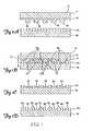
- a typical thermal imprint lithographic process for forming nano-dimensioned patterns/features in a substrate surfaceis illustrated with reference to the schematic, cross-sectional views of FIGS. 1 (A)- 1 (D).
- a mold 10also known as a stamper or imprinter
- main or support body 12having upper and lower opposed surfaces
- molding layer 14also referred to as an imprinting surface
- molding layer 14includes a plurality of features 16 having a desired shape or surface contour.
- a substrate or workpiece 18 carrying a thin film layer 20 on an upper surface thereofis positioned below, and in facing relation to the molding layer 14 .
- Thin film layer 20e.g., of polymethyl methacrylate (PMMA), may be formed on the substrate/workpiece surface by any appropriate technique, e.g., spin casting.
- PMMApolymethyl methacrylate
- FIG. 1 (B)Adverting to FIG. 1 (B), shown therein is a compressive molding step, wherein mold 10 is pressed into the thin film layer 20 in the direction shown by arrow 22 , so as to form depressed, i.e., compressed, regions 24 .
- features 16 of the molding layer 14are not pressed all of the way into the thin film layer 20 and thus do not contact the surface of the underlying substrate 18 .
- the top surface portions 24 a of thin film 20may contact depressed surface portions 16 a of molding layer 14 .
- the top surface portions 24 asubstantially conform to the shape of the depressed surface portions 16 a , for example, flat.
- FIG. 1 (C)shows the cross-sectional surface contour of the thin film layer 20 following removal of mold 10 .
- the molded, or imprinted, thin film layer 20includes a plurality of recesses formed at compressed regions 24 which generally conform to the shape or surface contour of features 16 of the molding layer 14 .
- the surface-molded workpieceis subjected to processing to remove the compressed portions 24 of thin film 20 to selectively expose portions 28 of the underlying substrate 18 separated by raised features 26 .
- Selective removal of the compressed portions 24may be accomplished by any appropriate process, e.g., reactive ion etching (RIE), wet chemical etching, or ion or electron beam irradiation.
- RIEreactive ion etching
- the thus-patterned thin film layer 20may subsequently be utilized as an etch mask or irradiation mask for selective removal of the exposed substrate portions 28 , after which the patterned thin film layer 20 is itself selectively removed, leaving a patterned substrate 18 .
- the above-described imprint lithographic processingis capable of providing sub-micron-dimensioned features, as by utilizing a mold 10 provided with patterned features 16 comprising pillars, holes, trenches, etc., by means of e-beam lithography, RIE, or other appropriate patterning method. Typical depths of features 16 range from about 5 to about 500 nm, depending upon the desired lateral dimension.
- the material of the molding layer 14is typically selected to be hard relative to the thin film layer 20 , the latter typically comprising a thermoplastic material which is softened when heated.
- suitable materials for use as the molding layer 14include metals, dielectrics, semiconductors, ceramics, and composite materials.
- Suitable materials for use as thin film layer 20include thermoplastic polymers which can be heated to above their glass temperature, T g , such that the material exhibits low viscosity and enhanced flow.
- thermoplastic polymer materialsWhile nanoimprint lithographic techniques, such as described above, afford the possibility of a low-cost, mass manufacturing technology for fabrication of sub-100 nm structures, features, etc., for semiconductor ICs, integrated optical, magnetic, and mechanical devices, the problem of non-uniform replication and sticking of the thermoplastic polymer materials to the molding layer 14 when the latter is applied to a large-area substrate, e.g., as in the formation of servo patterns in 95 mm diameter disks used in hard disk drives, arising from differences in thermal expansion/contraction characteristics of the mold and substrate materials, has not heretofore been addressed.
- stamper/imprinterthe components of the imprinting system, i.e., substrate, resist layer, and mold or imprint tool (referred to in the art as a stamper/imprinter) to undergo large thermal swings or cycling, e.g., within a range of about 100° C.
- Imprint lithography toolsvariously termed molds, stampers, imprinters, masks, etc., conventionally have been fabricated by electroforming nickel (Ni) or copper (Cu) onto a master plate comprising a patterned photoresist, or by etching through a substrate, e.g., of silicon (Si), coated with a layer of patterned photoresist.
- Ninickel
- Cucopper
- the former techniqueis typically utilized in the replication of vinyl audio records and optical disks; whereas the latter technique has been utilized to fabricate tools having very small feature sizes, e.g., ⁇ 20 nm, by means of e-beam techniques.
- thermal expansion/contraction characteristics of these materialsare substantially and significantly different from those of either the glass, ceramic, glass-ceramic composite, or nickel-phosphorus coated aluminum (Al/Ni—P) substrates typically utilized in fabricating magnetic media for use in hard disk drives, which differences in thermal expansion/contraction characteristics disadvantageously result in the above-mentioned degradation in imprint quality, e.g., resist deformation, poor mold release (sticking) causing resist peeling, and damage leading to loss of dimensional integrity, pattern/feature definition, etc.
- thermal lithographic imprintingAnother drawback associated with thermal lithographic imprinting is the very long heating and cooling times required for performing the pattern embossing process, which disadvantageously results in correspondingly long cycles times (on the order of several minutes) and significantly increased cost when forming part of a high product throughput manufacturing process, e.g., manufacture of substrates for hard disk magnetic recording media.
- the present inventionaddresses and solves problems and difficulties such as degradation of replication quality due to resist deformation, peeling, and poor mold release, attendant upon the use of thermal imprint lithography for pattern definition in substrate/workpiece surfaces, such as in the fabrication of hard disk substrates with integrally formed servo patterns, while maintaining full capability with all aspects of conventional automated manufacturing technology for pattern formation by imprint lithography. Further, the methodology and means afforded by the present invention enjoy diverse utility in the imprint lithographic patterning of a variety of substrates and workpieces.
- An advantage of the present inventionis an improved method of performing imprint lithography.
- Another advantage of the present inventionis an improved method of forming a servo pattern in a surface of a substrate for a hard disk recording medium.
- Yet another advantage of the present inventionis an improved substrate for a hard disk magnetic recording medium including a servo pattern formed in a surface thereof.
- the foregoing and other advantagesare obtained in part by a method of performing imprint lithography of a surface of a workpiece including a substrate and a layer of an imprintable resist material, wherein a stamper/imprinter comprised of a material having thermal expansion characteristics different from the material of the substrate is utilized for embossing a desired pattern in the workpiece surface, the method comprising conducting the embossing at room temperature, whereby deleterious effects arising from differences in thermal expansion/contraction characteristics of the stamper/imprinter and workpiece are avoided.
- the stamper/imprintercomprises:
- the support body (a) and the imprinting surface (b) of the stamper/imprinterare composed of the same material, e.g., a metal material, such as nickel (Ni); whereas, according to other particular embodiments of the present invention, the support body (a) and the imprinting surface (b) are composed of different materials, e.g., the imprinting surface (b) is made of silicon (Si) and the support body (b) is made of a metal.
- the imprinting surface (b)has a negative image of a servo pattern for a recording medium formed therein, e.g., a negative image of a servo pattern for a disk-shaped magnetic recording medium;
- the workpieceincludes a substrate for a hard disk magnetic recording medium, the substrate having a surface and comprising a material selected from the group consisting of glass, ceramics, glass-ceramics composites, polymers, metals, and metal alloys;
- the workpiecefurther includes a layer of an imprintable resist material overlying the substrate surface and presenting an exposed upper surface; and the servo pattern is embossed at room temperature in the exposed upper surface of the layer of resist material to form a servo-patterned resist layer.
- the thickness of the layer of resist materialis less than the depth of the features of the negative image of the servo pattern of the imprinting surface (b); and the method further comprises steps of selectively forming the servo pattern in the hard disk substrate material utilizing the servo-patterned resist layer as an etch mask or irradiation mask and selectively removing the servo-patterned resist layer subsequent to forming of the servo pattern in the hard disk substrate material.
- Embodiments of the present inventioninclude performing the room temperature embossing of the servo pattern in the layer of resist material comprising utilizing a press for high pressure urging of the imprinting surface of the stamper/imprinter against the exposed upper surface of the layer of resist material.
- Another aspect of the present inventionis a method of forming a servo pattern in the surface of a substrate for a magnetic recording medium, comprising the steps of:
- the methodfurther comprises the steps of:
- step (e)selectively removing the servo-patterned layer of resist material subsequent to performing step (d).
- step (a)comprises providing a disk-shaped substrate comprising a material selected from the group consisting of glass, ceramics, glass-ceramics composites, polymers, metals, and metal alloys; and step (b) comprises providing a stamper/imprinter wherein at least the imprinting surface is comprised of a metal material.
- step (a)comprises providing a disk-shaped substrate comprised of glass or NiP-coated Al; and step (b) comprises providing a stamper/imprinter including an imprinting surface comprised of Ni.
- step (a)comprises providing a workpiece including a resist layer having a thickness less than the depth of the features of the negative image of the servo pattern in the imprinting surface of the imprinter/stamper; and step (c) comprises performing room temperature embossing of the servo pattern utilizing a press for high pressure urging of the imprinting surface of the stamper/imprinter against the exposed upper surface of the layer of resist material.
- Still another aspect of the present inventionis a substrate for a hard disk magnetic recording medium, comprising a servo pattern formed in a surface thereof by a process comprising room temperature embossing of the servo pattern in a layer of an imprintable resist material overlying the substrate surface.
- FIGS. 1 (A)- 1 (D)are schematic, simplified cross-sectional views illustrating a process sequence for performing thermal imprint lithography of a thin resist film on a substrate (workpiece) according to the conventional art;
- FIG. 2is a photomicrograph of a resist-coated glass substrate imprinted with a servo pattern according to the room temperature process of the present invention.
- FIG. 3is a photomicrograph of the servo-patterned glass substrate of FIG. 2 after reactive ion etching (RIE) of the glass substrate and resist removal.
- RIEreactive ion etching
- the present inventionaddresses and solves problems attendant upon the use of stampers/imprinters and workpieces of different materials, hence different thermal expansion/contraction characteristics, when performing imprint lithography at elevated temperatures, e.g., nanoimprint lithography for forming submicron-dimensioned patterns and features in substrate surfaces utilized in various technologies such as semiconductor IC processing and magnetic recording media manufacture, and is based upon the discovery that degradation of pattern replication fidelity arising from resist damage, loss of dimensional accuracy, peeling, sticking, etc., can be eliminated, or at least minimized, so as to facilitate accurate, high quality replication of a desired feature or pattern in an imprintable layer, e.g., of a resist material, on a workpiece surface.
- an imprintable layere.g., of a resist material
- imprinting of the pattern in a resist layer overlying a substrate of a workpieceis accomplished at room temperature, i.e., without thermal input, by means of a device, e.g., a hydraulic press, capable of urging the imprinting surface of the stamper/imprinter against the exposed upper surface of the imprintable resist layer with a sufficient force, e.g., ⁇ 20,000-40,000 lbs. onto a 95 mm diameter disk, such that the surface of the resist layer accurately conforms to the surface topography of the stamper/imprinter.
- a devicee.g., a hydraulic press
- the inventive methodologyavoids, or at least minimizes, the above-described deleterious effects on replication fidelity associated with the differences in thermal expansion/characteristics of the stamper/imprinter and the workpiece arising from the different materials utilized for the former and the latter.
- a metal-based stamper/imprinterwas utilized for forming a servo pattern in a disk-shaped glass substrate of a type typically employed as a substrate for a hard disk magnetic recording medium.
- a 95 mm diameter glass disk substratewas spin-coated with an approximately 130 nm thick layer of an imprintable photoresist material (Shipley 1805) from approximately a 15. mm radius to the outer diameter, after which the resist-coated substrate was pre-baked at 90° C. for approximately 40 min.
- a metal-based stampercomprising a Ni imprinting surface having a negative image of a servo pattern for a disk-shaped magnetic recording medium formed therein was prepared.
- the feature (“format”) height of the negative image servo patternwas greater than the thickness of the resist layer, i.e., about 160 mm.
- a resilient (rubber) padwas placed on the back surface of the substrate and another flat, polished steel plate was placed over the back side of the stamper/imprinter.
- the sandwich-type assemblywas then placed in a manually-actuated hydraulic press and a compressive force of about 20,000 lbs. was applied thereto for about 10 sec.
- the assembly with imprinted resist layerwas then removed from the press and disassembled.
- the resist layerwas determined to have a well-defined servo format pattern formed therein that replicated the negative image pattern of the imprinting surface of the stamper/imprinter with excellent fidelity, as is apparent from the photomicrograph of FIG. 2 .
- the imprinted workpiecewas then subjected to reactive ion etching (RIE) in a CHF 3 /Ar atmosphere at 450 Watts power for about 15 minutes to selectively etch the servo format pattern into the glass substrate, using the servo-patterned photoresist layer as an etch (or irradiation) mask.
- RIEreactive ion etching
- the remaining photoresist after RIEwas then removed by etching in a pure O 2 plasma at 200 Watts power for about 5 minutes.
- a metal-based stamper/imprinterwas utilized for forming a servo pattern in a disk-shaped metal substrate of a type typically employed as a substrate for a hard disk magnetic recording medium. More specifically, according to this example, an 84 mm diameter NiP-coated Al disk substrate was spin-coated with an about 90 nm thick layer of an imprintable photoresist material (Shipley 1805). An assembly of the coated disk and a stamper/imprinter including a Ni imprinting surface having a negative image of a servo pattern for a disk-shaped magnetic recording medium formed therein was prepared as in the first example and placed in an automatic hydraulic press (Carver) for 10 sec. at approximately 40,000 lbs.
- Carverautomatic hydraulic press
- the servo pattern of the imprinting surfacewas faithfully replicated in the imprintable resist layer in well-defined manner, after which the imprinted resist layer was utilized as an etch or irradiation mask for selectively forming the servo pattern in the underlying NiP/Al substrate, followed by removal of the residual resist layer.
- the stamper/imprintermay comprise different materials, e.g., an imprinting surface made of a patterned silicon (Si) layer overlying a metal support body or layer.
- the imprinting surfacemay be made of a material selected on the basis of its wear resistance, non-stick properties, and/or ease of surface patterning.
- the material of the imprinting surfacetherefore, may be substantially different from that of the underlying support body or layer, the latter material being selected on the basis of economic considerations, e.g., low cost, and physical properties, e.g., mechanical robustness.
- the inventive means and methodologyprovides for the performance of imprint lithography with improved replication fidelity and substantially reduced cycle times, i.e., on the order of about 10 sec., compared with cycle times of several minutes according to conventional thermal imprint lithographic processing at elevated temperatures.
- inventive methodologyreadily permits the use of stampers/imprinters and substrates/workpieces of different materials having substantially different thermal expansion/contraction characteristics, e.g., widely utilized stampers/imprinters with Ni imprinting surfaces can be readily employed for imprinting of glass and metal-based substrates/workpieces, e.g., Al-based substrates, such as are conventionally utilized in the fabrication of hard disk magnetic recording media.
- inventive methodologyis not limited to use as described above in the illustrative examples; rather, the invention can be practiced with a wide variety of substrates/workpieces, such as, for example, semiconductor substrates utilized in integrated circuit (IC) device manufacture, and the imprinted patterns capable of being formed by the invention are not limited to servo patterns for magnetic recording media, and may, for example, include metallization patterns of semiconductor IC devices.
- substrates/workpiecessuch as, for example, semiconductor substrates utilized in integrated circuit (IC) device manufacture
- imprinted patterns capable of being formed by the inventionare not limited to servo patterns for magnetic recording media, and may, for example, include metallization patterns of semiconductor IC devices.
Landscapes
- Engineering & Computer Science (AREA)
- Chemical & Material Sciences (AREA)
- Nanotechnology (AREA)
- Physics & Mathematics (AREA)
- General Physics & Mathematics (AREA)
- Crystallography & Structural Chemistry (AREA)
- Condensed Matter Physics & Semiconductors (AREA)
- Manufacturing & Machinery (AREA)
- Mathematical Physics (AREA)
- Theoretical Computer Science (AREA)
- Manufacturing Of Magnetic Record Carriers (AREA)
Abstract
Description
Claims (20)
Priority Applications (1)
| Application Number | Priority Date | Filing Date | Title |
|---|---|---|---|
| US09/966,105US6814898B1 (en) | 2000-10-17 | 2001-10-01 | Imprint lithography utilizing room temperature embossing |
Applications Claiming Priority (2)
| Application Number | Priority Date | Filing Date | Title |
|---|---|---|---|
| US24141800P | 2000-10-17 | 2000-10-17 | |
| US09/966,105US6814898B1 (en) | 2000-10-17 | 2001-10-01 | Imprint lithography utilizing room temperature embossing |
Publications (1)
| Publication Number | Publication Date |
|---|---|
| US6814898B1true US6814898B1 (en) | 2004-11-09 |
Family
ID=33312931
Family Applications (1)
| Application Number | Title | Priority Date | Filing Date |
|---|---|---|---|
| US09/966,105Expired - Fee RelatedUS6814898B1 (en) | 2000-10-17 | 2001-10-01 | Imprint lithography utilizing room temperature embossing |
Country Status (1)
| Country | Link |
|---|---|
| US (1) | US6814898B1 (en) |
Cited By (56)
| Publication number | Priority date | Publication date | Assignee | Title |
|---|---|---|---|---|
| US20030179481A1 (en)* | 2001-02-16 | 2003-09-25 | Mcneil Michael | Patterned medium |
| US20040211755A1 (en)* | 2003-01-07 | 2004-10-28 | Atsushi Yusa | Imprint manufacture method and apparatus, magnetic recording medium and its manufacture apparatus |
| US20050120545A1 (en)* | 2002-11-27 | 2005-06-09 | Wachenschwanz David E. | Magnetic discrete track recording disk |
| US20050238967A1 (en)* | 2004-04-27 | 2005-10-27 | The Board Of Trustees Of The University Of Illinois | Composite patterning devices for soft lithography |
| US20060079094A1 (en)* | 2004-10-09 | 2006-04-13 | Bianca Schreder | Method for microstructuring flat glass substrates |
| US20060110890A1 (en)* | 2004-11-19 | 2006-05-25 | International Business Machines Corporation | Cut-and-paste imprint lithographic mold and method therefor |
| US20060131785A1 (en)* | 2004-12-16 | 2006-06-22 | Asml Holding N.V. | System and method for patterning both sides of a substrate utilizing imprint lithography |
| US20060130678A1 (en)* | 2004-12-16 | 2006-06-22 | Asml Holding N.V. | Method and apparatus for imprint pattern replication |
| US20060130317A1 (en)* | 2004-12-16 | 2006-06-22 | Asml Holding, N.V. | Method and system for making a computer hard drive platen using a nano-plate |
| US20060131270A1 (en)* | 2004-12-16 | 2006-06-22 | Asml Holding, N.V. | Method and system for making a nano-plate for imprint lithography |
| US20060180805A1 (en)* | 2002-10-02 | 2006-08-17 | Norbert Lutz | Film comprising organic semiconductors |
| KR100633019B1 (en)* | 2004-12-24 | 2006-10-12 | 한국기계연구원 | Stamping and Substrate Separation Process in Microimprint Lithography Process and Its Apparatus |
| US20060255505A1 (en)* | 2005-05-11 | 2006-11-16 | Micron Technology, Inc. | Imprint templates for imprint lithography, and methods of patterning a plurality of substrates |
| US7147790B2 (en) | 2002-11-27 | 2006-12-12 | Komag, Inc. | Perpendicular magnetic discrete track recording disk |
| US20070032089A1 (en)* | 2004-06-04 | 2007-02-08 | The Board Of Trustees Of The University Of Illinois | Printable Semiconductor Structures and Related Methods of Making and Assembling |
| KR100693992B1 (en) | 2005-08-20 | 2007-03-12 | 이헌 | Nickel stamp and manufacturing method for easy release coating of self-aligned single layer |
| US20070059497A1 (en)* | 2002-05-08 | 2007-03-15 | Xudong Huang | Reversal imprint technique |
| US20070121375A1 (en)* | 2005-11-29 | 2007-05-31 | Asml Holding N.V. | System and method for forming nanodisks used in imprint lithography and nanodisk and memory disk formed thereby |
| US20070145613A1 (en)* | 2005-12-22 | 2007-06-28 | Tdk Corporation | Concave/convex pattern forming method and information recording medium manufacturing method |
| US20070257396A1 (en)* | 2006-05-05 | 2007-11-08 | Jian Wang | Device and method of forming nanoimprinted structures |
| US20080055581A1 (en)* | 2004-04-27 | 2008-03-06 | Rogers John A | Devices and methods for pattern generation by ink lithography |
| US20080084006A1 (en)* | 2006-10-10 | 2008-04-10 | Jun Gao | Hydraulic-facilitated contact lithography apparatus, system and method |
| US20080087636A1 (en)* | 2006-10-12 | 2008-04-17 | Wei Wu | Contact lithography apparatus and method |
| US20080131548A1 (en)* | 2006-12-01 | 2008-06-05 | Seagate Technology Llc | Thermal expansion compensated stampers/imprinters for fabricating patterned recording media |
| EP1972996A1 (en) | 2007-03-21 | 2008-09-24 | Erich Dipl.-Ing. Thallner | Method and device for generating a nanostructured disc |
| US20090199960A1 (en)* | 2004-06-04 | 2009-08-13 | Nuzzo Ralph G | Pattern Transfer Printing by Kinetic Control of Adhesion to an Elastomeric Stamp |
| US7972875B2 (en) | 2007-01-17 | 2011-07-05 | The Board Of Trustees Of The University Of Illinois | Optical systems fabricated by printing-based assembly |
| US7982296B2 (en) | 2004-06-04 | 2011-07-19 | The Board Of Trustees Of The University Of Illinois | Methods and devices for fabricating and assembling printable semiconductor elements |
| US8097926B2 (en) | 2008-10-07 | 2012-01-17 | Mc10, Inc. | Systems, methods, and devices having stretchable integrated circuitry for sensing and delivering therapy |
| US8198621B2 (en) | 2004-06-04 | 2012-06-12 | The Board Of Trustees Of The University Of Illinois | Stretchable form of single crystal silicon for high performance electronics on rubber substrates |
| US8367035B2 (en) | 2006-03-03 | 2013-02-05 | The Board Of Trustees Of The University Of Illinois | Methods of making spatially aligned nanotubes and nanotube arrays |
| US8372726B2 (en) | 2008-10-07 | 2013-02-12 | Mc10, Inc. | Methods and applications of non-planar imaging arrays |
| US8389862B2 (en) | 2008-10-07 | 2013-03-05 | Mc10, Inc. | Extremely stretchable electronics |
| US8470701B2 (en) | 2008-04-03 | 2013-06-25 | Advanced Diamond Technologies, Inc. | Printable, flexible and stretchable diamond for thermal management |
| US8552299B2 (en) | 2008-03-05 | 2013-10-08 | The Board Of Trustees Of The University Of Illinois | Stretchable and foldable electronic devices |
| US8666471B2 (en) | 2010-03-17 | 2014-03-04 | The Board Of Trustees Of The University Of Illinois | Implantable biomedical devices on bioresorbable substrates |
| US8865489B2 (en) | 2009-05-12 | 2014-10-21 | The Board Of Trustees Of The University Of Illinois | Printed assemblies of ultrathin, microscale inorganic light emitting diodes for deformable and semitransparent displays |
| US8886334B2 (en) | 2008-10-07 | 2014-11-11 | Mc10, Inc. | Systems, methods, and devices using stretchable or flexible electronics for medical applications |
| US8934965B2 (en) | 2011-06-03 | 2015-01-13 | The Board Of Trustees Of The University Of Illinois | Conformable actively multiplexed high-density surface electrode array for brain interfacing |
| US8946683B2 (en) | 2008-06-16 | 2015-02-03 | The Board Of Trustees Of The University Of Illinois | Medium scale carbon nanotube thin film integrated circuits on flexible plastic substrates |
| US9159635B2 (en) | 2011-05-27 | 2015-10-13 | Mc10, Inc. | Flexible electronic structure |
| US9171794B2 (en) | 2012-10-09 | 2015-10-27 | Mc10, Inc. | Embedding thin chips in polymer |
| US9289132B2 (en) | 2008-10-07 | 2016-03-22 | Mc10, Inc. | Catheter balloon having stretchable integrated circuitry and sensor array |
| US9442285B2 (en) | 2011-01-14 | 2016-09-13 | The Board Of Trustees Of The University Of Illinois | Optical component array having adjustable curvature |
| JP2016192519A (en)* | 2015-03-31 | 2016-11-10 | 株式会社協同インターナショナル | Replica mold and manufacturing method thereof |
| US9554484B2 (en) | 2012-03-30 | 2017-01-24 | The Board Of Trustees Of The University Of Illinois | Appendage mountable electronic devices conformable to surfaces |
| US9691873B2 (en) | 2011-12-01 | 2017-06-27 | The Board Of Trustees Of The University Of Illinois | Transient devices designed to undergo programmable transformations |
| US9723122B2 (en) | 2009-10-01 | 2017-08-01 | Mc10, Inc. | Protective cases with integrated electronics |
| US9765934B2 (en) | 2011-05-16 | 2017-09-19 | The Board Of Trustees Of The University Of Illinois | Thermally managed LED arrays assembled by printing |
| US9936574B2 (en) | 2009-12-16 | 2018-04-03 | The Board Of Trustees Of The University Of Illinois | Waterproof stretchable optoelectronics |
| US10441185B2 (en) | 2009-12-16 | 2019-10-15 | The Board Of Trustees Of The University Of Illinois | Flexible and stretchable electronic systems for epidermal electronics |
| US10918298B2 (en) | 2009-12-16 | 2021-02-16 | The Board Of Trustees Of The University Of Illinois | High-speed, high-resolution electrophysiology in-vivo using conformal electronics |
| US10925543B2 (en) | 2015-11-11 | 2021-02-23 | The Board Of Trustees Of The University Of Illinois | Bioresorbable silicon electronics for transient implants |
| US11029198B2 (en) | 2015-06-01 | 2021-06-08 | The Board Of Trustees Of The University Of Illinois | Alternative approach for UV sensing |
| US11118965B2 (en) | 2015-06-01 | 2021-09-14 | The Board Of Trustees Of The University Of Illinois | Miniaturized electronic systems with wireless power and near-field communication capabilities |
| US20220088834A1 (en)* | 2016-12-22 | 2022-03-24 | Illumina, Inc. | Imprinting apparatus |
Citations (3)
| Publication number | Priority date | Publication date | Assignee | Title |
|---|---|---|---|---|
| US4900111A (en)* | 1989-02-15 | 1990-02-13 | American Bank Note Holographics, Inc. | Embossed holograms formed on hard metal surfaces |
| US5279689A (en)* | 1989-06-30 | 1994-01-18 | E. I. Du Pont De Nemours And Company | Method for replicating holographic optical elements |
| US5427599A (en)* | 1987-06-09 | 1995-06-27 | International Business Machines Corporation | System for stamping an optical storage disk |
- 2001
- 2001-10-01USUS09/966,105patent/US6814898B1/ennot_activeExpired - Fee Related
Patent Citations (3)
| Publication number | Priority date | Publication date | Assignee | Title |
|---|---|---|---|---|
| US5427599A (en)* | 1987-06-09 | 1995-06-27 | International Business Machines Corporation | System for stamping an optical storage disk |
| US4900111A (en)* | 1989-02-15 | 1990-02-13 | American Bank Note Holographics, Inc. | Embossed holograms formed on hard metal surfaces |
| US5279689A (en)* | 1989-06-30 | 1994-01-18 | E. I. Du Pont De Nemours And Company | Method for replicating holographic optical elements |
Cited By (132)
| Publication number | Priority date | Publication date | Assignee | Title |
|---|---|---|---|---|
| US7471484B2 (en) | 2001-02-16 | 2008-12-30 | Wd Media, Inc. | Patterned medium and recording head |
| US7019924B2 (en) | 2001-02-16 | 2006-03-28 | Komag, Incorporated | Patterned medium and recording head |
| US20030179481A1 (en)* | 2001-02-16 | 2003-09-25 | Mcneil Michael | Patterned medium |
| US20060139814A1 (en)* | 2001-02-16 | 2006-06-29 | David Wachenschwanz | Patterned medium and recording head |
| US20070059497A1 (en)* | 2002-05-08 | 2007-03-15 | Xudong Huang | Reversal imprint technique |
| US7655498B2 (en)* | 2002-10-02 | 2010-02-02 | Leonhard Kurz Stiftung & Co. Kg | Film comprising organic semiconductors |
| US20060180805A1 (en)* | 2002-10-02 | 2006-08-17 | Norbert Lutz | Film comprising organic semiconductors |
| US7608193B2 (en) | 2002-11-27 | 2009-10-27 | Wd Media, Inc. | Perpendicular magnetic discrete track recording disk |
| US20050120545A1 (en)* | 2002-11-27 | 2005-06-09 | Wachenschwanz David E. | Magnetic discrete track recording disk |
| US7656615B2 (en) | 2002-11-27 | 2010-02-02 | Wd Media, Inc. | Perpendicular magnetic recording disk with a soft magnetic layer having a discrete track recording pattern |
| US20070039922A1 (en)* | 2002-11-27 | 2007-02-22 | Wachenschwanz David E | Perpendicular magnetic discrete track recording disk |
| US7549209B2 (en) | 2002-11-27 | 2009-06-23 | Wd Media, Inc. | Method of fabricating a magnetic discrete track recording disk |
| US20070041306A1 (en)* | 2002-11-27 | 2007-02-22 | Wachenschwanz David E | Perpendicular magnetic discrete track recording disk |
| US7147790B2 (en) | 2002-11-27 | 2006-12-12 | Komag, Inc. | Perpendicular magnetic discrete track recording disk |
| US20040211755A1 (en)* | 2003-01-07 | 2004-10-28 | Atsushi Yusa | Imprint manufacture method and apparatus, magnetic recording medium and its manufacture apparatus |
| US7736558B2 (en)* | 2003-01-07 | 2010-06-15 | Hitachi Maxell, Ltd. | Imprint manufacture method |
| CN102004393B (en)* | 2004-04-27 | 2013-05-01 | 伊利诺伊大学评议会 | Composite patterning devices for soft lithography |
| WO2005104756A3 (en)* | 2004-04-27 | 2009-04-02 | Univ Illinois | Composite patterning devices for soft lithography |
| US20050238967A1 (en)* | 2004-04-27 | 2005-10-27 | The Board Of Trustees Of The University Of Illinois | Composite patterning devices for soft lithography |
| US20080055581A1 (en)* | 2004-04-27 | 2008-03-06 | Rogers John A | Devices and methods for pattern generation by ink lithography |
| US7195733B2 (en)* | 2004-04-27 | 2007-03-27 | The Board Of Trustees Of The University Of Illinois | Composite patterning devices for soft lithography |
| US9761444B2 (en) | 2004-06-04 | 2017-09-12 | The Board Of Trustees Of The University Of Illinois | Methods and devices for fabricating and assembling printable semiconductor elements |
| US8754396B2 (en) | 2004-06-04 | 2014-06-17 | The Board Of Trustees Of The University Of Illinois | Stretchable form of single crystal silicon for high performance electronics on rubber substrates |
| US7799699B2 (en) | 2004-06-04 | 2010-09-21 | The Board Of Trustees Of The University Of Illinois | Printable semiconductor structures and related methods of making and assembling |
| US12074213B2 (en) | 2004-06-04 | 2024-08-27 | The Board Of Trustees Of The University Of Illinois | Methods and devices for fabricating and assembling printable semiconductor elements |
| US9515025B2 (en) | 2004-06-04 | 2016-12-06 | The Board Of Trustees Of The University Of Illinois | Stretchable form of single crystal silicon for high performance electronics on rubber substrates |
| US8198621B2 (en) | 2004-06-04 | 2012-06-12 | The Board Of Trustees Of The University Of Illinois | Stretchable form of single crystal silicon for high performance electronics on rubber substrates |
| US20090199960A1 (en)* | 2004-06-04 | 2009-08-13 | Nuzzo Ralph G | Pattern Transfer Printing by Kinetic Control of Adhesion to an Elastomeric Stamp |
| US11456258B2 (en) | 2004-06-04 | 2022-09-27 | The Board Of Trustees Of The University Of Illinois | Stretchable form of single crystal silicon for high performance electronics on rubber substrates |
| US11088268B2 (en) | 2004-06-04 | 2021-08-10 | The Board Of Trustees Of The University Of Illinois | Methods and devices for fabricating and assembling printable semiconductor elements |
| US8440546B2 (en) | 2004-06-04 | 2013-05-14 | The Board Of Trustees Of The University Of Illinois | Methods and devices for fabricating and assembling printable semiconductor elements |
| US9450043B2 (en) | 2004-06-04 | 2016-09-20 | The Board Of Trustees Of The University Of Illinois | Methods and devices for fabricating and assembling printable semiconductor elements |
| US10374072B2 (en) | 2004-06-04 | 2019-08-06 | The Board Of Trustees Of The University Of Illinois | Methods and devices for fabricating and assembling printable semiconductor elements |
| US8664699B2 (en) | 2004-06-04 | 2014-03-04 | The Board Of Trustees Of The University Of Illinois | Methods and devices for fabricating and assembling printable semiconductor elements |
| US8394706B2 (en) | 2004-06-04 | 2013-03-12 | The Board Of Trustees Of The University Of Illinois | Printable semiconductor structures and related methods of making and assembling |
| US8039847B2 (en) | 2004-06-04 | 2011-10-18 | The Board Of Trustees Of The University Of Illinois | Printable semiconductor structures and related methods of making and assembling |
| US7982296B2 (en) | 2004-06-04 | 2011-07-19 | The Board Of Trustees Of The University Of Illinois | Methods and devices for fabricating and assembling printable semiconductor elements |
| US10204864B2 (en) | 2004-06-04 | 2019-02-12 | The Board Of Trustees Of The University Of Illinois | Stretchable form of single crystal silicon for high performance electronics on rubber substrates |
| US9768086B2 (en) | 2004-06-04 | 2017-09-19 | The Board Of Trustees Of The University Of Illinois | Methods and devices for fabricating and assembling printable semiconductor elements |
| US7943491B2 (en) | 2004-06-04 | 2011-05-17 | The Board Of Trustees Of The University Of Illinois | Pattern transfer printing by kinetic control of adhesion to an elastomeric stamp |
| US9105555B2 (en) | 2004-06-04 | 2015-08-11 | The Board Of Trustees Of The University Of Illinois | Stretchable form of single crystal silicon for high performance electronics on rubber substrates |
| US20070032089A1 (en)* | 2004-06-04 | 2007-02-08 | The Board Of Trustees Of The University Of Illinois | Printable Semiconductor Structures and Related Methods of Making and Assembling |
| US7476623B2 (en)* | 2004-10-09 | 2009-01-13 | Schott Ag | Method for microstructuring flat glass substrates |
| US20080257860A1 (en)* | 2004-10-09 | 2008-10-23 | Bianca Schreder | Method for microstructuring flat glass substrates |
| US20060079094A1 (en)* | 2004-10-09 | 2006-04-13 | Bianca Schreder | Method for microstructuring flat glass substrates |
| US20080116602A1 (en)* | 2004-11-19 | 2008-05-22 | International Business Machines Corporation | Cut-and-paste imprint lithographic mold and method therefor |
| US7344955B2 (en)* | 2004-11-19 | 2008-03-18 | International Business Machines Corporation | Cut-and-paste imprint lithographic mold and method therefor |
| US20060110890A1 (en)* | 2004-11-19 | 2006-05-25 | International Business Machines Corporation | Cut-and-paste imprint lithographic mold and method therefor |
| US7776709B2 (en)* | 2004-11-19 | 2010-08-17 | International Business Machines Corporation | Cut-and-paste imprint lithographic mold and method therefor |
| US20080163769A1 (en)* | 2004-12-16 | 2008-07-10 | Asml Holding N.V. | System and method for patterning both sides of a substrate utilizing imprint lithography |
| US7409759B2 (en) | 2004-12-16 | 2008-08-12 | Asml Holding N.V. | Method for making a computer hard drive platen using a nano-plate |
| US7331283B2 (en) | 2004-12-16 | 2008-02-19 | Asml Holding N.V. | Method and apparatus for imprint pattern replication |
| US7363854B2 (en) | 2004-12-16 | 2008-04-29 | Asml Holding N.V. | System and method for patterning both sides of a substrate utilizing imprint lithography |
| US20060130678A1 (en)* | 2004-12-16 | 2006-06-22 | Asml Holding N.V. | Method and apparatus for imprint pattern replication |
| US20060130317A1 (en)* | 2004-12-16 | 2006-06-22 | Asml Holding, N.V. | Method and system for making a computer hard drive platen using a nano-plate |
| US20060131270A1 (en)* | 2004-12-16 | 2006-06-22 | Asml Holding, N.V. | Method and system for making a nano-plate for imprint lithography |
| US7882780B2 (en) | 2004-12-16 | 2011-02-08 | Asml Holding N.V. | System and method for patterning both sides of a substrate utilizing imprint lithography |
| US20060131785A1 (en)* | 2004-12-16 | 2006-06-22 | Asml Holding N.V. | System and method for patterning both sides of a substrate utilizing imprint lithography |
| US7410591B2 (en) | 2004-12-16 | 2008-08-12 | Asml Holding N.V. | Method and system for making a nano-plate for imprint lithography |
| KR100633019B1 (en)* | 2004-12-24 | 2006-10-12 | 한국기계연구원 | Stamping and Substrate Separation Process in Microimprint Lithography Process and Its Apparatus |
| US20060255505A1 (en)* | 2005-05-11 | 2006-11-16 | Micron Technology, Inc. | Imprint templates for imprint lithography, and methods of patterning a plurality of substrates |
| US7767129B2 (en) | 2005-05-11 | 2010-08-03 | Micron Technology, Inc. | Imprint templates for imprint lithography, and methods of patterning a plurality of substrates |
| KR100693992B1 (en) | 2005-08-20 | 2007-03-12 | 이헌 | Nickel stamp and manufacturing method for easy release coating of self-aligned single layer |
| US20080285428A1 (en)* | 2005-11-29 | 2008-11-20 | Asml Holding N.V. | System and Method for Forming Nanodisks Used in Imprint Lithography and Nanodisk and Memory Disk Formed Thereby |
| US7399422B2 (en) | 2005-11-29 | 2008-07-15 | Asml Holding N.V. | System and method for forming nanodisks used in imprint lithography and nanodisk and memory disk formed thereby |
| US20070121375A1 (en)* | 2005-11-29 | 2007-05-31 | Asml Holding N.V. | System and method for forming nanodisks used in imprint lithography and nanodisk and memory disk formed thereby |
| US7701668B2 (en) | 2005-11-29 | 2010-04-20 | Asml Holding Nv | System and method for forming nanodisks used in imprint lithography and nanodisk and memory disk formed thereby |
| US20070145613A1 (en)* | 2005-12-22 | 2007-06-28 | Tdk Corporation | Concave/convex pattern forming method and information recording medium manufacturing method |
| US8367035B2 (en) | 2006-03-03 | 2013-02-05 | The Board Of Trustees Of The University Of Illinois | Methods of making spatially aligned nanotubes and nanotube arrays |
| US20070257396A1 (en)* | 2006-05-05 | 2007-11-08 | Jian Wang | Device and method of forming nanoimprinted structures |
| US7830498B2 (en) | 2006-10-10 | 2010-11-09 | Hewlett-Packard Development Company, L.P. | Hydraulic-facilitated contact lithography apparatus, system and method |
| US20080084006A1 (en)* | 2006-10-10 | 2008-04-10 | Jun Gao | Hydraulic-facilitated contact lithography apparatus, system and method |
| US7768628B2 (en) | 2006-10-12 | 2010-08-03 | Hewlett-Packard Development Company, L.P. | Contact lithography apparatus and method |
| US20080087636A1 (en)* | 2006-10-12 | 2008-04-17 | Wei Wu | Contact lithography apparatus and method |
| US20120058312A1 (en)* | 2006-12-01 | 2012-03-08 | Seagate Technology Llc | Thermal compensated stampers/imprinters |
| US7919029B2 (en)* | 2006-12-01 | 2011-04-05 | Seagate Technology Llc | Thermal compensated stampers/imprinters |
| US20080131548A1 (en)* | 2006-12-01 | 2008-06-05 | Seagate Technology Llc | Thermal expansion compensated stampers/imprinters for fabricating patterned recording media |
| US8323018B2 (en)* | 2006-12-01 | 2012-12-04 | Seagate Technology Llc | Thermal compensated stampers/imprinters |
| US11309305B2 (en) | 2007-01-17 | 2022-04-19 | The Board Of Trustees Of The University Of Illinois | Optical systems fabricated by printing-based assembly |
| US9601671B2 (en) | 2007-01-17 | 2017-03-21 | The Board Of Trustees Of The University Of Illinois | Optical systems fabricated by printing-based assembly |
| US10424572B2 (en) | 2007-01-17 | 2019-09-24 | The Board Of Trustees Of The University Of Illinois | Optical systems fabricated by printing-based assembly |
| US10504882B2 (en) | 2007-01-17 | 2019-12-10 | The Board Of Trustees Of The University Of Illinois | Optical systems fabricated by printing-based assembly |
| US12136620B2 (en) | 2007-01-17 | 2024-11-05 | The Board Of Trustees Of The University Of Illinois | Optical systems fabricated by printing-based assembly |
| US9117940B2 (en) | 2007-01-17 | 2015-08-25 | The Board Of Trustees Of The University Of Illinois | Optical systems fabricated by printing-based assembly |
| US7972875B2 (en) | 2007-01-17 | 2011-07-05 | The Board Of Trustees Of The University Of Illinois | Optical systems fabricated by printing-based assembly |
| US8722458B2 (en) | 2007-01-17 | 2014-05-13 | The Board Of Trustees Of The University Of Illinois | Optical systems fabricated by printing-based assembly |
| US10361180B2 (en) | 2007-01-17 | 2019-07-23 | The Board Of Trustees Of The University Of Illinois | Optical systems fabricated by printing-based assembly |
| US8142701B2 (en) | 2007-03-21 | 2012-03-27 | Erich Thallner | Method and device for producing a nanopatterned disc |
| US20080233331A1 (en)* | 2007-03-21 | 2008-09-25 | Erich Thallner | Method and device for producing a nanopatterned disc |
| EP1972996A1 (en) | 2007-03-21 | 2008-09-24 | Erich Dipl.-Ing. Thallner | Method and device for generating a nanostructured disc |
| US8591794B2 (en) | 2007-03-21 | 2013-11-26 | Erich Thallner | Method and device for producing a nanopatterned disc |
| US8905772B2 (en) | 2008-03-05 | 2014-12-09 | The Board Of Trustees Of The University Of Illinois | Stretchable and foldable electronic devices |
| US8552299B2 (en) | 2008-03-05 | 2013-10-08 | The Board Of Trustees Of The University Of Illinois | Stretchable and foldable electronic devices |
| US10292261B2 (en) | 2008-03-05 | 2019-05-14 | The Board Of Trustees Of The University Of Illinois | Stretchable and foldable electronic devices |
| US10064269B2 (en) | 2008-03-05 | 2018-08-28 | The Board Of Trustees Of The University Of Illinois | Stretchable and foldable electronic devices |
| US8470701B2 (en) | 2008-04-03 | 2013-06-25 | Advanced Diamond Technologies, Inc. | Printable, flexible and stretchable diamond for thermal management |
| US8946683B2 (en) | 2008-06-16 | 2015-02-03 | The Board Of Trustees Of The University Of Illinois | Medium scale carbon nanotube thin film integrated circuits on flexible plastic substrates |
| US9516758B2 (en) | 2008-10-07 | 2016-12-06 | Mc10, Inc. | Extremely stretchable electronics |
| US9289132B2 (en) | 2008-10-07 | 2016-03-22 | Mc10, Inc. | Catheter balloon having stretchable integrated circuitry and sensor array |
| US8389862B2 (en) | 2008-10-07 | 2013-03-05 | Mc10, Inc. | Extremely stretchable electronics |
| US9012784B2 (en) | 2008-10-07 | 2015-04-21 | Mc10, Inc. | Extremely stretchable electronics |
| US8886334B2 (en) | 2008-10-07 | 2014-11-11 | Mc10, Inc. | Systems, methods, and devices using stretchable or flexible electronics for medical applications |
| US8372726B2 (en) | 2008-10-07 | 2013-02-12 | Mc10, Inc. | Methods and applications of non-planar imaging arrays |
| US8536667B2 (en) | 2008-10-07 | 2013-09-17 | Mc10, Inc. | Systems, methods, and devices having stretchable integrated circuitry for sensing and delivering therapy |
| US8097926B2 (en) | 2008-10-07 | 2012-01-17 | Mc10, Inc. | Systems, methods, and devices having stretchable integrated circuitry for sensing and delivering therapy |
| US9647171B2 (en) | 2009-05-12 | 2017-05-09 | The Board Of Trustees Of The University Of Illinois | Printed assemblies of ultrathin, microscale inorganic light emitting diodes for deformable and semitransparent displays |
| US10546841B2 (en) | 2009-05-12 | 2020-01-28 | The Board Of Trustees Of The University Of Illinois | Printed assemblies of ultrathin, microscale inorganic light emitting diodes for deformable and semitransparent displays |
| US8865489B2 (en) | 2009-05-12 | 2014-10-21 | The Board Of Trustees Of The University Of Illinois | Printed assemblies of ultrathin, microscale inorganic light emitting diodes for deformable and semitransparent displays |
| US9723122B2 (en) | 2009-10-01 | 2017-08-01 | Mc10, Inc. | Protective cases with integrated electronics |
| US11057991B2 (en) | 2009-12-16 | 2021-07-06 | The Board Of Trustees Of The University Of Illinois | Waterproof stretchable optoelectronics |
| US9936574B2 (en) | 2009-12-16 | 2018-04-03 | The Board Of Trustees Of The University Of Illinois | Waterproof stretchable optoelectronics |
| US10918298B2 (en) | 2009-12-16 | 2021-02-16 | The Board Of Trustees Of The University Of Illinois | High-speed, high-resolution electrophysiology in-vivo using conformal electronics |
| US10441185B2 (en) | 2009-12-16 | 2019-10-15 | The Board Of Trustees Of The University Of Illinois | Flexible and stretchable electronic systems for epidermal electronics |
| US8666471B2 (en) | 2010-03-17 | 2014-03-04 | The Board Of Trustees Of The University Of Illinois | Implantable biomedical devices on bioresorbable substrates |
| US9986924B2 (en) | 2010-03-17 | 2018-06-05 | The Board Of Trustees Of The University Of Illinois | Implantable biomedical devices on bioresorbable substrates |
| US9442285B2 (en) | 2011-01-14 | 2016-09-13 | The Board Of Trustees Of The University Of Illinois | Optical component array having adjustable curvature |
| US9765934B2 (en) | 2011-05-16 | 2017-09-19 | The Board Of Trustees Of The University Of Illinois | Thermally managed LED arrays assembled by printing |
| US9159635B2 (en) | 2011-05-27 | 2015-10-13 | Mc10, Inc. | Flexible electronic structure |
| US8934965B2 (en) | 2011-06-03 | 2015-01-13 | The Board Of Trustees Of The University Of Illinois | Conformable actively multiplexed high-density surface electrode array for brain interfacing |
| US10349860B2 (en) | 2011-06-03 | 2019-07-16 | The Board Of Trustees Of The University Of Illinois | Conformable actively multiplexed high-density surface electrode array for brain interfacing |
| US9691873B2 (en) | 2011-12-01 | 2017-06-27 | The Board Of Trustees Of The University Of Illinois | Transient devices designed to undergo programmable transformations |
| US10396173B2 (en) | 2011-12-01 | 2019-08-27 | The Board Of Trustees Of The University Of Illinois | Transient devices designed to undergo programmable transformations |
| US9554484B2 (en) | 2012-03-30 | 2017-01-24 | The Board Of Trustees Of The University Of Illinois | Appendage mountable electronic devices conformable to surfaces |
| US10357201B2 (en) | 2012-03-30 | 2019-07-23 | The Board Of Trustees Of The University Of Illinois | Appendage mountable electronic devices conformable to surfaces |
| US10052066B2 (en) | 2012-03-30 | 2018-08-21 | The Board Of Trustees Of The University Of Illinois | Appendage mountable electronic devices conformable to surfaces |
| US9171794B2 (en) | 2012-10-09 | 2015-10-27 | Mc10, Inc. | Embedding thin chips in polymer |
| JP2016192519A (en)* | 2015-03-31 | 2016-11-10 | 株式会社協同インターナショナル | Replica mold and manufacturing method thereof |
| US11029198B2 (en) | 2015-06-01 | 2021-06-08 | The Board Of Trustees Of The University Of Illinois | Alternative approach for UV sensing |
| US11118965B2 (en) | 2015-06-01 | 2021-09-14 | The Board Of Trustees Of The University Of Illinois | Miniaturized electronic systems with wireless power and near-field communication capabilities |
| US10925543B2 (en) | 2015-11-11 | 2021-02-23 | The Board Of Trustees Of The University Of Illinois | Bioresorbable silicon electronics for transient implants |
| US20220088834A1 (en)* | 2016-12-22 | 2022-03-24 | Illumina, Inc. | Imprinting apparatus |
| US12157252B2 (en)* | 2016-12-22 | 2024-12-03 | Illumina, Inc. | Imprinting apparatus including silicon master with a plurality of nanofeatures and an anti-stick layer having a cyclosiloxane and method of forming |
Similar Documents
| Publication | Publication Date | Title |
|---|---|---|
| US6814898B1 (en) | Imprint lithography utilizing room temperature embossing | |
| US6949199B1 (en) | Heat-transfer-stamp process for thermal imprint lithography | |
| US6869557B1 (en) | Multi-level stamper for improved thermal imprint lithography | |
| US7448860B2 (en) | Surface modified stamper for imprint lithography | |
| McClelland et al. | Nanoscale patterning of magnetic islands by imprint lithography using a flexible mold | |
| JP4712370B2 (en) | Composite stamper for imprint lithography | |
| US6753130B1 (en) | Resist removal from patterned recording media | |
| US5772905A (en) | Nanoimprint lithography | |
| Komuro et al. | Imprint characteristics by photo-induced solidification of liquid polymer | |
| US7378028B2 (en) | Method for fabricating patterned magnetic recording media | |
| US8323018B2 (en) | Thermal compensated stampers/imprinters | |
| US8109752B2 (en) | Imprinting stamper and method of manufacturing the same | |
| US20050082700A1 (en) | Dry passivation process for stamper/imprinter family making for patterned recording media | |
| US20100009025A1 (en) | Mold for pattern transfer | |
| CN100437759C (en) | Method and apparatus for manufacturing plate-like structure | |
| WO2007099907A1 (en) | Imprinting mold and method of imprinting | |
| JPH0736239B2 (en) | Optical storage disk manufacturing method and manufacturing apparatus | |
| JP2006148055A (en) | Method for performing hot embossing lithography | |
| JP4058425B2 (en) | Stamper, imprint method, and information recording medium manufacturing method | |
| JP2008126450A (en) | Mold, manufacturing method thereof, and magnetic recording medium | |
| CN100407372C (en) | Imprint method and manufacturing method of information recording medium | |
| EP0939399A3 (en) | Optical recording medium, and method of manufacturing same | |
| US7105280B1 (en) | Utilizing permanent master for making stampers/imprinters for patterning of recording media | |
| Wagner et al. | Nanoimprint lithography: Review of aspects and applications | |
| JP2009226750A (en) | Mold structure for imprint, imprinting method using mold structure for imprint, magnetic recording medium, and its manufacturing method |
Legal Events
| Date | Code | Title | Description |
|---|---|---|---|
| AS | Assignment | Owner name:SEAGATE TECHNOLOGY LLC, CALIFORNIA Free format text:ASSIGNMENT OF ASSIGNORS INTEREST;ASSIGNORS:DEEMAN, NEIL;GAUZNER, GENNADY;REEL/FRAME:012228/0486;SIGNING DATES FROM 20010824 TO 20010925 | |
| AS | Assignment | Owner name:JPMORGAN CHASE BANK, AS COLLATERAL AGENT, NEW YORK Free format text:SECURITY AGREEMENT;ASSIGNOR:SEAGATE TECHNOLOGY LLC;REEL/FRAME:013177/0001 Effective date:20020513 Owner name:JPMORGAN CHASE BANK, AS COLLATERAL AGENT,NEW YORK Free format text:SECURITY AGREEMENT;ASSIGNOR:SEAGATE TECHNOLOGY LLC;REEL/FRAME:013177/0001 Effective date:20020513 | |
| AS | Assignment | Owner name:SEAGATE TECHNOLOGY LLC, CALIFORNIA Free format text:RELEASE OF SECURITY INTERESTS IN PATENT RIGHTS;ASSIGNOR:JPMORGAN CHASE BANK, N.A. (FORMERLY KNOWN AS THE CHASE MANHATTAN BANK AND JPMORGAN CHASE BANK), AS ADMINISTRATIVE AGENT;REEL/FRAME:016967/0001 Effective date:20051130 | |
| FPAY | Fee payment | Year of fee payment:4 | |
| AS | Assignment | Owner name:WELLS FARGO BANK, NATIONAL ASSOCIATION, AS COLLATERAL AGENT AND SECOND PRIORITY REPRESENTATIVE, CALIFORNIA Free format text:SECURITY AGREEMENT;ASSIGNORS:MAXTOR CORPORATION;SEAGATE TECHNOLOGY LLC;SEAGATE TECHNOLOGY INTERNATIONAL;REEL/FRAME:022757/0017 Effective date:20090507 Owner name:JPMORGAN CHASE BANK, N.A., AS ADMINISTRATIVE AGENT AND FIRST PRIORITY REPRESENTATIVE, NEW YORK Free format text:SECURITY AGREEMENT;ASSIGNORS:MAXTOR CORPORATION;SEAGATE TECHNOLOGY LLC;SEAGATE TECHNOLOGY INTERNATIONAL;REEL/FRAME:022757/0017 Effective date:20090507 Owner name:JPMORGAN CHASE BANK, N.A., AS ADMINISTRATIVE AGENT Free format text:SECURITY AGREEMENT;ASSIGNORS:MAXTOR CORPORATION;SEAGATE TECHNOLOGY LLC;SEAGATE TECHNOLOGY INTERNATIONAL;REEL/FRAME:022757/0017 Effective date:20090507 Owner name:WELLS FARGO BANK, NATIONAL ASSOCIATION, AS COLLATE Free format text:SECURITY AGREEMENT;ASSIGNORS:MAXTOR CORPORATION;SEAGATE TECHNOLOGY LLC;SEAGATE TECHNOLOGY INTERNATIONAL;REEL/FRAME:022757/0017 Effective date:20090507 | |
| AS | Assignment | Owner name:SEAGATE TECHNOLOGY INTERNATIONAL, CALIFORNIA Free format text:RELEASE;ASSIGNOR:JPMORGAN CHASE BANK, N.A., AS ADMINISTRATIVE AGENT;REEL/FRAME:025662/0001 Effective date:20110114 Owner name:SEAGATE TECHNOLOGY LLC, CALIFORNIA Free format text:RELEASE;ASSIGNOR:JPMORGAN CHASE BANK, N.A., AS ADMINISTRATIVE AGENT;REEL/FRAME:025662/0001 Effective date:20110114 Owner name:MAXTOR CORPORATION, CALIFORNIA Free format text:RELEASE;ASSIGNOR:JPMORGAN CHASE BANK, N.A., AS ADMINISTRATIVE AGENT;REEL/FRAME:025662/0001 Effective date:20110114 Owner name:SEAGATE TECHNOLOGY HDD HOLDINGS, CALIFORNIA Free format text:RELEASE;ASSIGNOR:JPMORGAN CHASE BANK, N.A., AS ADMINISTRATIVE AGENT;REEL/FRAME:025662/0001 Effective date:20110114 | |
| AS | Assignment | Owner name:THE BANK OF NOVA SCOTIA, AS ADMINISTRATIVE AGENT, CANADA Free format text:SECURITY AGREEMENT;ASSIGNOR:SEAGATE TECHNOLOGY LLC;REEL/FRAME:026010/0350 Effective date:20110118 Owner name:THE BANK OF NOVA SCOTIA, AS ADMINISTRATIVE AGENT, Free format text:SECURITY AGREEMENT;ASSIGNOR:SEAGATE TECHNOLOGY LLC;REEL/FRAME:026010/0350 Effective date:20110118 | |
| FPAY | Fee payment | Year of fee payment:8 | |
| AS | Assignment | Owner name:EVAULT INC. (F/K/A I365 INC.), CALIFORNIA Free format text:TERMINATION AND RELEASE OF SECURITY INTEREST IN PATENT RIGHTS;ASSIGNOR:WELLS FARGO BANK, NATIONAL ASSOCIATION, AS COLLATERAL AGENT AND SECOND PRIORITY REPRESENTATIVE;REEL/FRAME:030833/0001 Effective date:20130312 Owner name:SEAGATE TECHNOLOGY INTERNATIONAL, CAYMAN ISLANDS Free format text:TERMINATION AND RELEASE OF SECURITY INTEREST IN PATENT RIGHTS;ASSIGNOR:WELLS FARGO BANK, NATIONAL ASSOCIATION, AS COLLATERAL AGENT AND SECOND PRIORITY REPRESENTATIVE;REEL/FRAME:030833/0001 Effective date:20130312 Owner name:SEAGATE TECHNOLOGY US HOLDINGS, INC., CALIFORNIA Free format text:TERMINATION AND RELEASE OF SECURITY INTEREST IN PATENT RIGHTS;ASSIGNOR:WELLS FARGO BANK, NATIONAL ASSOCIATION, AS COLLATERAL AGENT AND SECOND PRIORITY REPRESENTATIVE;REEL/FRAME:030833/0001 Effective date:20130312 Owner name:SEAGATE TECHNOLOGY LLC, CALIFORNIA Free format text:TERMINATION AND RELEASE OF SECURITY INTEREST IN PATENT RIGHTS;ASSIGNOR:WELLS FARGO BANK, NATIONAL ASSOCIATION, AS COLLATERAL AGENT AND SECOND PRIORITY REPRESENTATIVE;REEL/FRAME:030833/0001 Effective date:20130312 | |
| REMI | Maintenance fee reminder mailed | ||
| LAPS | Lapse for failure to pay maintenance fees | ||
| STCH | Information on status: patent discontinuation | Free format text:PATENT EXPIRED DUE TO NONPAYMENT OF MAINTENANCE FEES UNDER 37 CFR 1.362 | |
| FP | Lapsed due to failure to pay maintenance fee | Effective date:20161109 | |
| AS | Assignment | Owner name:SEAGATE TECHNOLOGY PUBLIC LIMITED COMPANY, CALIFORNIA Free format text:RELEASE BY SECURED PARTY;ASSIGNOR:THE BANK OF NOVA SCOTIA;REEL/FRAME:072193/0001 Effective date:20250303 Owner name:SEAGATE TECHNOLOGY, CALIFORNIA Free format text:RELEASE BY SECURED PARTY;ASSIGNOR:THE BANK OF NOVA SCOTIA;REEL/FRAME:072193/0001 Effective date:20250303 Owner name:SEAGATE TECHNOLOGY HDD HOLDINGS, CALIFORNIA Free format text:RELEASE BY SECURED PARTY;ASSIGNOR:THE BANK OF NOVA SCOTIA;REEL/FRAME:072193/0001 Effective date:20250303 Owner name:I365 INC., CALIFORNIA Free format text:RELEASE BY SECURED PARTY;ASSIGNOR:THE BANK OF NOVA SCOTIA;REEL/FRAME:072193/0001 Effective date:20250303 Owner name:SEAGATE TECHNOLOGY LLC, CALIFORNIA Free format text:RELEASE BY SECURED PARTY;ASSIGNOR:THE BANK OF NOVA SCOTIA;REEL/FRAME:072193/0001 Effective date:20250303 Owner name:SEAGATE TECHNOLOGY INTERNATIONAL, CAYMAN ISLANDS Free format text:RELEASE BY SECURED PARTY;ASSIGNOR:THE BANK OF NOVA SCOTIA;REEL/FRAME:072193/0001 Effective date:20250303 Owner name:SEAGATE HDD CAYMAN, CAYMAN ISLANDS Free format text:RELEASE BY SECURED PARTY;ASSIGNOR:THE BANK OF NOVA SCOTIA;REEL/FRAME:072193/0001 Effective date:20250303 Owner name:SEAGATE TECHNOLOGY (US) HOLDINGS, INC., CALIFORNIA Free format text:RELEASE BY SECURED PARTY;ASSIGNOR:THE BANK OF NOVA SCOTIA;REEL/FRAME:072193/0001 Effective date:20250303 |