US6813293B2 - Long wavelength VCSEL with tunnel junction, and implant - Google Patents
Long wavelength VCSEL with tunnel junction, and implantDownload PDFInfo
- Publication number
- US6813293B2 US6813293B2US10/301,380US30138002AUS6813293B2US 6813293 B2US6813293 B2US 6813293B2US 30138002 AUS30138002 AUS 30138002AUS 6813293 B2US6813293 B2US 6813293B2
- Authority
- US
- United States
- Prior art keywords
- vcsel
- mirror
- tunnel junction
- region
- active region
- Prior art date
- Legal status (The legal status is an assumption and is not a legal conclusion. Google has not performed a legal analysis and makes no representation as to the accuracy of the status listed.)
- Expired - Fee Related
Links
- 239000007943implantSubstances0.000titleclaimsabstractdescription29
- 238000002955isolationMethods0.000claimsabstractdescription26
- 230000003647oxidationEffects0.000claimsabstractdescription21
- 238000007254oxidation reactionMethods0.000claimsabstractdescription21
- 239000000463materialSubstances0.000claimsdescription33
- 239000000758substrateSubstances0.000claimsdescription13
- 230000002093peripheral effectEffects0.000claims12
- 239000003989dielectric materialSubstances0.000claims2
- 230000005641tunnelingEffects0.000claims2
- 229910001218Gallium arsenideInorganic materials0.000description9
- VYPSYNLAJGMNEJ-UHFFFAOYSA-NSilicium dioxideChemical compoundO=[Si]=OVYPSYNLAJGMNEJ-UHFFFAOYSA-N0.000description8
- 229910000980Aluminium gallium arsenideInorganic materials0.000description5
- GWEVSGVZZGPLCZ-UHFFFAOYSA-NTitan oxideChemical compoundO=[Ti]=OGWEVSGVZZGPLCZ-UHFFFAOYSA-N0.000description4
- 229910052681coesiteInorganic materials0.000description4
- 229910052906cristobaliteInorganic materials0.000description4
- 150000002500ionsChemical class0.000description4
- 239000000377silicon dioxideSubstances0.000description4
- 125000006850spacer groupChemical group0.000description4
- 229910052682stishoviteInorganic materials0.000description4
- 229910052905tridymiteInorganic materials0.000description4
- 230000004888barrier functionEffects0.000description3
- XAGFODPZIPBFFR-UHFFFAOYSA-NaluminiumChemical compound[Al]XAGFODPZIPBFFR-UHFFFAOYSA-N0.000description2
- 229910052782aluminiumInorganic materials0.000description2
- PNEYBMLMFCGWSK-UHFFFAOYSA-Naluminium oxideInorganic materials[O-2].[O-2].[O-2].[Al+3].[Al+3]PNEYBMLMFCGWSK-UHFFFAOYSA-N0.000description2
- 229910052593corundumInorganic materials0.000description2
- 238000000034methodMethods0.000description2
- 239000000203mixtureSubstances0.000description2
- 238000012986modificationMethods0.000description2
- 230000004048modificationEffects0.000description2
- 230000003287optical effectEffects0.000description2
- 229910001845yogo sapphireInorganic materials0.000description2
- 229910000530Gallium indium arsenideInorganic materials0.000description1
- 230000005684electric fieldEffects0.000description1
- 238000009713electroplatingMethods0.000description1
- 238000002513implantationMethods0.000description1
- 230000000737periodic effectEffects0.000description1
Images


Classifications
- H—ELECTRICITY
- H01—ELECTRIC ELEMENTS
- H01S—DEVICES USING THE PROCESS OF LIGHT AMPLIFICATION BY STIMULATED EMISSION OF RADIATION [LASER] TO AMPLIFY OR GENERATE LIGHT; DEVICES USING STIMULATED EMISSION OF ELECTROMAGNETIC RADIATION IN WAVE RANGES OTHER THAN OPTICAL
- H01S5/00—Semiconductor lasers
- H01S5/10—Construction or shape of the optical resonator, e.g. extended or external cavity, coupled cavities, bent-guide, varying width, thickness or composition of the active region
- H01S5/18—Surface-emitting [SE] lasers, e.g. having both horizontal and vertical cavities
- H01S5/183—Surface-emitting [SE] lasers, e.g. having both horizontal and vertical cavities having only vertical cavities, e.g. vertical cavity surface-emitting lasers [VCSEL]
- H01S5/18308—Surface-emitting [SE] lasers, e.g. having both horizontal and vertical cavities having only vertical cavities, e.g. vertical cavity surface-emitting lasers [VCSEL] having a special structure for lateral current or light confinement
- H—ELECTRICITY
- H01—ELECTRIC ELEMENTS
- H01S—DEVICES USING THE PROCESS OF LIGHT AMPLIFICATION BY STIMULATED EMISSION OF RADIATION [LASER] TO AMPLIFY OR GENERATE LIGHT; DEVICES USING STIMULATED EMISSION OF ELECTROMAGNETIC RADIATION IN WAVE RANGES OTHER THAN OPTICAL
- H01S5/00—Semiconductor lasers
- H01S5/04—Processes or apparatus for excitation, e.g. pumping, e.g. by electron beams
- H01S5/042—Electrical excitation ; Circuits therefor
- H01S5/0425—Electrodes, e.g. characterised by the structure
- H01S5/04254—Electrodes, e.g. characterised by the structure characterised by the shape
- H—ELECTRICITY
- H01—ELECTRIC ELEMENTS
- H01S—DEVICES USING THE PROCESS OF LIGHT AMPLIFICATION BY STIMULATED EMISSION OF RADIATION [LASER] TO AMPLIFY OR GENERATE LIGHT; DEVICES USING STIMULATED EMISSION OF ELECTROMAGNETIC RADIATION IN WAVE RANGES OTHER THAN OPTICAL
- H01S5/00—Semiconductor lasers
- H01S5/04—Processes or apparatus for excitation, e.g. pumping, e.g. by electron beams
- H01S5/042—Electrical excitation ; Circuits therefor
- H01S5/0425—Electrodes, e.g. characterised by the structure
- H01S5/04256—Electrodes, e.g. characterised by the structure characterised by the configuration
- H01S5/04257—Electrodes, e.g. characterised by the structure characterised by the configuration having positive and negative electrodes on the same side of the substrate
- H—ELECTRICITY
- H01—ELECTRIC ELEMENTS
- H01S—DEVICES USING THE PROCESS OF LIGHT AMPLIFICATION BY STIMULATED EMISSION OF RADIATION [LASER] TO AMPLIFY OR GENERATE LIGHT; DEVICES USING STIMULATED EMISSION OF ELECTROMAGNETIC RADIATION IN WAVE RANGES OTHER THAN OPTICAL
- H01S5/00—Semiconductor lasers
- H01S5/10—Construction or shape of the optical resonator, e.g. extended or external cavity, coupled cavities, bent-guide, varying width, thickness or composition of the active region
- H01S5/18—Surface-emitting [SE] lasers, e.g. having both horizontal and vertical cavities
- H01S5/183—Surface-emitting [SE] lasers, e.g. having both horizontal and vertical cavities having only vertical cavities, e.g. vertical cavity surface-emitting lasers [VCSEL]
- H01S5/18308—Surface-emitting [SE] lasers, e.g. having both horizontal and vertical cavities having only vertical cavities, e.g. vertical cavity surface-emitting lasers [VCSEL] having a special structure for lateral current or light confinement
- H01S5/18311—Surface-emitting [SE] lasers, e.g. having both horizontal and vertical cavities having only vertical cavities, e.g. vertical cavity surface-emitting lasers [VCSEL] having a special structure for lateral current or light confinement using selective oxidation
- H—ELECTRICITY
- H01—ELECTRIC ELEMENTS
- H01S—DEVICES USING THE PROCESS OF LIGHT AMPLIFICATION BY STIMULATED EMISSION OF RADIATION [LASER] TO AMPLIFY OR GENERATE LIGHT; DEVICES USING STIMULATED EMISSION OF ELECTROMAGNETIC RADIATION IN WAVE RANGES OTHER THAN OPTICAL
- H01S5/00—Semiconductor lasers
- H01S5/10—Construction or shape of the optical resonator, e.g. extended or external cavity, coupled cavities, bent-guide, varying width, thickness or composition of the active region
- H01S5/18—Surface-emitting [SE] lasers, e.g. having both horizontal and vertical cavities
- H01S5/183—Surface-emitting [SE] lasers, e.g. having both horizontal and vertical cavities having only vertical cavities, e.g. vertical cavity surface-emitting lasers [VCSEL]
- H01S5/18308—Surface-emitting [SE] lasers, e.g. having both horizontal and vertical cavities having only vertical cavities, e.g. vertical cavity surface-emitting lasers [VCSEL] having a special structure for lateral current or light confinement
- H01S5/18316—Airgap confined
- H—ELECTRICITY
- H01—ELECTRIC ELEMENTS
- H01S—DEVICES USING THE PROCESS OF LIGHT AMPLIFICATION BY STIMULATED EMISSION OF RADIATION [LASER] TO AMPLIFY OR GENERATE LIGHT; DEVICES USING STIMULATED EMISSION OF ELECTROMAGNETIC RADIATION IN WAVE RANGES OTHER THAN OPTICAL
- H01S5/00—Semiconductor lasers
- H01S5/10—Construction or shape of the optical resonator, e.g. extended or external cavity, coupled cavities, bent-guide, varying width, thickness or composition of the active region
- H01S5/18—Surface-emitting [SE] lasers, e.g. having both horizontal and vertical cavities
- H01S5/183—Surface-emitting [SE] lasers, e.g. having both horizontal and vertical cavities having only vertical cavities, e.g. vertical cavity surface-emitting lasers [VCSEL]
- H01S5/18308—Surface-emitting [SE] lasers, e.g. having both horizontal and vertical cavities having only vertical cavities, e.g. vertical cavity surface-emitting lasers [VCSEL] having a special structure for lateral current or light confinement
- H01S5/18322—Position of the structure
- H01S5/1833—Position of the structure with more than one structure
- H—ELECTRICITY
- H01—ELECTRIC ELEMENTS
- H01S—DEVICES USING THE PROCESS OF LIGHT AMPLIFICATION BY STIMULATED EMISSION OF RADIATION [LASER] TO AMPLIFY OR GENERATE LIGHT; DEVICES USING STIMULATED EMISSION OF ELECTROMAGNETIC RADIATION IN WAVE RANGES OTHER THAN OPTICAL
- H01S5/00—Semiconductor lasers
- H01S5/10—Construction or shape of the optical resonator, e.g. extended or external cavity, coupled cavities, bent-guide, varying width, thickness or composition of the active region
- H01S5/18—Surface-emitting [SE] lasers, e.g. having both horizontal and vertical cavities
- H01S5/183—Surface-emitting [SE] lasers, e.g. having both horizontal and vertical cavities having only vertical cavities, e.g. vertical cavity surface-emitting lasers [VCSEL]
- H01S5/18361—Structure of the reflectors, e.g. hybrid mirrors
- H01S5/18369—Structure of the reflectors, e.g. hybrid mirrors based on dielectric materials
- H—ELECTRICITY
- H01—ELECTRIC ELEMENTS
- H01S—DEVICES USING THE PROCESS OF LIGHT AMPLIFICATION BY STIMULATED EMISSION OF RADIATION [LASER] TO AMPLIFY OR GENERATE LIGHT; DEVICES USING STIMULATED EMISSION OF ELECTROMAGNETIC RADIATION IN WAVE RANGES OTHER THAN OPTICAL
- H01S5/00—Semiconductor lasers
- H01S5/10—Construction or shape of the optical resonator, e.g. extended or external cavity, coupled cavities, bent-guide, varying width, thickness or composition of the active region
- H01S5/18—Surface-emitting [SE] lasers, e.g. having both horizontal and vertical cavities
- H01S5/183—Surface-emitting [SE] lasers, e.g. having both horizontal and vertical cavities having only vertical cavities, e.g. vertical cavity surface-emitting lasers [VCSEL]
- H01S5/18361—Structure of the reflectors, e.g. hybrid mirrors
- H01S5/18377—Structure of the reflectors, e.g. hybrid mirrors comprising layers of different kind of materials, e.g. combinations of semiconducting with dielectric or metallic layers
- H—ELECTRICITY
- H01—ELECTRIC ELEMENTS
- H01S—DEVICES USING THE PROCESS OF LIGHT AMPLIFICATION BY STIMULATED EMISSION OF RADIATION [LASER] TO AMPLIFY OR GENERATE LIGHT; DEVICES USING STIMULATED EMISSION OF ELECTROMAGNETIC RADIATION IN WAVE RANGES OTHER THAN OPTICAL
- H01S5/00—Semiconductor lasers
- H01S5/20—Structure or shape of the semiconductor body to guide the optical wave ; Confining structures perpendicular to the optical axis, e.g. index or gain guiding, stripe geometry, broad area lasers, gain tailoring, transverse or lateral reflectors, special cladding structures, MQW barrier reflection layers
- H01S5/2054—Methods of obtaining the confinement
- H01S5/2059—Methods of obtaining the confinement by means of particular conductivity zones, e.g. obtained by particle bombardment or diffusion
- H01S5/2063—Methods of obtaining the confinement by means of particular conductivity zones, e.g. obtained by particle bombardment or diffusion obtained by particle bombardment
- H—ELECTRICITY
- H01—ELECTRIC ELEMENTS
- H01S—DEVICES USING THE PROCESS OF LIGHT AMPLIFICATION BY STIMULATED EMISSION OF RADIATION [LASER] TO AMPLIFY OR GENERATE LIGHT; DEVICES USING STIMULATED EMISSION OF ELECTROMAGNETIC RADIATION IN WAVE RANGES OTHER THAN OPTICAL
- H01S5/00—Semiconductor lasers
- H01S5/30—Structure or shape of the active region; Materials used for the active region
- H01S5/305—Structure or shape of the active region; Materials used for the active region characterised by the doping materials used in the laser structure
- H01S5/3095—Tunnel junction
Definitions
- the present inventionpertains to vertical cavity surface emitting lasers (VCSELs) and particularly to tunnel junction VCSELs having long wavelengths, namely, 1200 to 1800 nanometer wavelengths.
- VCSELsvertical cavity surface emitting lasers
- tunnel junction VCSELshaving long wavelengths, namely, 1200 to 1800 nanometer wavelengths.
- a long wavelength VCSEL having a tunnel junction and a thick mirror layeris difficult to isolate because of the high doping used in the tunnel junction.
- Island isolation or trenchescan provide direct current (D.C.) isolation for such VCSELs.
- D.C.direct current
- an implantneeds to be used; however, it will not adequately compensate the tunnel junction. Because the implant can go deeper than the tunnel junction into the p region and down to the active region it can form an insulating region under the tunnel junction which reduces the capacitance.
- Some VCSEL isolationis shown in U.S. Pat. No. 5,903,588.
- U.S. Pat. No. 5,903,588issued May 11, 1999, and entitled “Laser with a Selectively Changed Current Confining Layer,” is expressly incorporated herein by reference into this description.
- An isolation implant used for isolation of a VCSELshould go through and past the tunnel junction of the VCSEL into and optimally through the p layer. This implant results in a semi-insulating region that reduces capacitance under the tunnel junction. Internal trenches about the VCSEL aperture can be utilized to reduce a required oxidation distance and thus reduce variability of the aperture diameter.
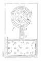
- FIG. 1shows a cross-section of a VCSEL having tunnel junction, with implant and island or trench isolation
- FIG. 2shows a cross-section of another configuration of a tunnel junction VCSEL
- FIG. 3 areveals a layout having a trench around a VCSEL including a bond pad and its connecting bridge to the VCSEL;
- FIG. 3 bshows a bond pad having several bridges connecting it to the VCSEL.
- FIG. 4 areveals interior trenches on the VCSEL device for reducing a required oxidation distance
- FIG. 4 bshows a cross-section of several interior trenches on the VCSEL device
- FIG. 5shows a bonding pad and the connecting bridge to a VCSEL also having interior oxidation trenches.
- FIG. 1shows a manufacturable structure of a VCSEL having deep implant isolation.
- a VCSEL that emits light having a 1200 to 1800 nanometer (nm) wavelengthis described, though the same structures and techniques adjusted for the wavelength are advantageous for other wavelength VCSELs such as 850 nm, 980 nm or 660 nm VCSELs.
- a distributed Bragg reflector N-mirror 11is situated on a substrate 36 .
- Mirror 11may be composed of 30 to 50 pairs of layers. Each layer of the pair is about one-fourth of the optical design wavelength ( ⁇ ) of light to be emitted by the VCSEL.
- Each pair of layersmay be InGaAsP and InP, AlGaAsSb and InP, or AlGaPSb and InP, respectively, for a 1550 nm InP VCSEL. These layers are lattice matched to InP and may or may not be fully N-doped. They may be partially doped for the intra-cavity type of device.
- An active region 12 having InAlGaAs strained quantum wells and InAlAs barriers, also of a strained composition,is on mirror 11 . Active region 12 is not doped or is unintentionally doped.
- An oxidizable layer(s) or region 13is on active region 12 . Layer(s) 13 has InAlAs material.
- the composition of layer 13may be high in Al content and thus easily oxidizable. Another kind of oxidizable material may be present in layer 13 . Lateral oxidation regions 23 are made and extend to the periphery of the inside aperture of current confinement. The material of region 13 may or may not be lattice matched. Region 13 is P-doped. A tunnel junction 14 may be on region 13 . This junction 14 has a highly doped P material adjacent ( ⁇ 1e20/cm3) to a highly doped N material ( ⁇ 3e19/cm3) that results in the junction. The materials may include InAlGaAs and InP. Another distributed Bragg reflector N-mirror 15 is on tunnel junction 14 . It may have about 35 pairs of layers of InGaAsP and InP, InAlGaAs and InP or InAlGaAs and InAlAs. These layers of mirror 15 may be lattice material to InP.
- a 1310 nm VCSEL 10may be a GaAs substrate based device.
- an appropriate substrate 36may be an N mirror 11 having from 25 to 40 pairs of layers of AlGaAs and GaAs or AlAs and GaAs, respectively. These materials are lattice matched and may or may not be fully N-doped. They may be partially doped for the intra-cavity type of device.
- an active region 12On mirror 11 is an active region 12 having quantum wells and barriers. There may be one to five quantum wells. There may be included in active region 12 a spacer layer above or below the quantum wells to extend the cavity multiples of half wavelengths. The spacer may have periodic doping peaked at the nulls of the optical field.
- the material of active region 12may include quantum wells of InGaAsN or InGaAsNSb, barrier layers of GaAs or GaAsN, GaAsSbN or a combination thereof, and confining layers of GaAs, AlGaAs, GaAsP or some combination thereof.
- the quantum wells of region 12are not doped or may be unintentionally doped.
- On region 12may be a region 13 having a partially oxidized layer that extends inward up to the periphery of where the current of an operating VCSEL 10 may be confined is centered on the null of the electric field.
- the materialmay include AlGaAs which has a high proportion of Al for lateral oxidation of the region.
- the materialmay be lattice matched and P-doped.
- a tunnel junction 14having highly doped P and N materials adjacent to each other to form a junction.
- the materialsmay be GaAs, AlGaAs or InGaAs. They may be or may not be lattice matched.
- an N mirror 15On tunnel junction 14 is an N mirror 15 .
- Mirror 15may have 16 to 25 pairs of layers of AlGaAs and GaAs and may contain a spacer which is a multiple of half wavelengths thick which may be periodically doped.
- a 1550 nm VCSEL 10may be a GaAs substrate based device.
- the material structure of this VCSELmay be the same as that of the 1310 nm GaAs VCSEL.
- the content distribution of the various materialsmay vary from one illustrative embodiment to another.
- VCSEL 10 of FIG. 1may be structured as an island with volume 18 of material removed or with a trench 19 around it or at least partially around it. Both types of structures are illustrated on the right and left sides, respectively, of FIG. 1 .
- Island 20is formed by the removal of material from volume 18 .
- Island 20 or trench 19is around at least active region 12 of VCSEL 10 and may provide tunnel junction 14 with D.C. isolation.
- Island 20 or trench 19may be used as an entry or source for lateral oxidation 23 to provide added isolation. Oxidation trenches 23 provide current confinement and thus may reduce variability in the diameter of the aperture.
- an isolation implant of volumes 21 and 22may be utilized.
- Implants 21 and 22are of sufficient depth to create a semi-insulating isolation to reduce the capacitance between tunnel junction 14 and the substrate. Buried implant 21 may go down through tunnel junction 14 and through a region including tunnel junction 14 and the quantum wells of active region 12 . The implant may be through more layers or regions, including down past active region 12 . Implant species may include H + ions, D + ions or He ++ ions. The energy range of an implant may be between 35 KeV and 2000 KeV. The energy dose of the implanting may be between 1E14 and 5E16 atoms/cm 2 and is optimally about 7E14 atoms/cm3.
- FIG. 2shows a VCSEL 30 having an upper mirror structure different than that of VCSEL 10 .
- VCSEL 30may have a spacer in the active region and/or one of the mirrors as in VCSEL 10 noted above.
- VCSEL 30has an N mirror 11 on a substrate 36 and an active region 12 on mirror 11 .
- On active region 12is an oxidation region 13 with lateral oxidized trenches 23 .
- Oxidation region 13is p-doped.
- region 13is tunnel junction 14 . Up to this point, the material and numbers of pairs of layers may be the same as those of VCSEL 10 .
- upper N-mirror 15may have a stack of 11 pairs of layers at a maximum.
- the materials of these layersmay be the same as those of mirror 15 of VCSEL 10 .
- That structuremay be an island 24 .
- a mirror structure 25that is an extension of mirror 15 .
- Itis an island 26 relative to the top of mirror 15 .
- Around island 26may be a contact 27 on top of mirror 15 .
- implant 21can reach down into active layer 12 .
- Implant 22may be situated in a portion of mirror 11 about or outside the perimeter of island 24 .
- Onemay do the same depth implant into or past active region 12 in VCSEL 10 as in VCSEL 30 with more energy but availability of implanters with sufficient energy may be a problem.
- a distinguishing feature between VCSEL 10 and VCSEL 30is the shorter mirror 15 with a dielectric mirror 25 stack or island 26 on mirror 15 of island 24 .
- Mirror 25may have 3 to 4 pairs of TiO 2 and SiO 2 , 2 to 3 pairs of Si and SiO 2 , 2 to 3 pairs of Si and Al 2 O 3 , or 4 to 5 pairs of TiO 2 and Al 2 O 3 , respectively.
- a contact 16On top of mirror 15 of VCSEL 10 is a contact 16 and the rest of the top surface of mirror 15 has a layer 17 of dielectric such as, for example, SiO 2 .
- a layer 17 of dielectricsuch as, for example, SiO 2 .
- contact 27 and mirror 25On the top of mirror 15 of VCSEL 30 is contact 27 and mirror 25 , as noted above.
- a layer 28 of dielectric on stack 25may be, for example, SiO 2 .
- Another contactmay be at the bottom of substrate 36 but may be brought up to be connectable from the top of the respective VCSEL 10 or 30 . In both VCSELs, the dielectric may cover light aperture 37 and not block the emitted light.
- FIG. 3 ashows VCSEL 10 having a bonding pad 29 and bridging connection 31 .
- device 10 or 30may be made without bridging between the bond pad and the device by taking advantage of the buried implant that goes at least through and under the tunnel junction, but which may be also elsewhere in the chip.
- Trench 19 in FIG. 3 agoes around VCSEL 10 and under bridge 31 at an area 38 close to its connection with contact 16 .
- Bridge 31at area 38 over trench 19 , may be an air bridge which might be made with the removal of sacrificial material beneath it, or it may be on a planarization layer, or have a trench filling under it or it may be electroplated with a patterned electroplating technique.
- a dielectric 32Around and under bonding pad 29 and its connecting bridge 31 to contact 16 may be a dielectric 32 .
- Dielectric 32may be contiguous with dielectric 17 of VCSEL 10 .
- Dielectric 17is situated over VCSEL 10 light aperture 37 .
- Dielectric 32might not be used in this pad 29 configuration.
- Trench 19goes around pad 29 and along the sides of bridge 31 , but on the periphery of dielectric 32 if pad 29 utilizes a dielectric.
- the dielectricmay provide both reduced capacitance and D.C. isolation of the VCSEL.
- VCSEL 10 of FIG. 3 amay have interior trenches like those of VCSEL 10 in FIG. 4 a.
- FIG. 3 bshows VCSEL 10 having several bridges 39 connecting bonding pad 29 to contact 16 .
- VCSEL 10 of this Figuremay have interior trenches like trenches 33 of VCSEL 10 in FIG. 4 a as described below.
- VCSEL 10 of FIG. 3 bmay also have a trench at least around a portion of its perimeter.
- FIG. 4 areveals VCSEL 10 having interior oxidation trenches 33 .
- VCSEL 30 of FIG. 2may also have trenches 33 .
- FIG. 4 bis a cross-section of trenches 33 which extend through top mirror 15 , tunnel junction 14 and oxidizable layer 13 having, for example, a high content of aluminum.
- Trenches 33may extend into or past active area 12 .
- Trenches 33enable oxidation in various layers, particularly layer 13 , having a high proportion of aluminum or other easily oxidizable material, to better provide isolation for tunnel junction 14 and current confinement.
- Trenches 33may define aperture 37 .
- FIG. 5shows not only interior trenches 33 of VCSEL 10 but also trenches 34 along connecting bridge 31 and trenches 35 in pad 29 .
- the layers from mirror 15 of VCSEL 10 down to substrate 36may be present through that portion of pad 29 and bridge 31 .
- trenches 34 and 35may go down to oxidizable layer 13 .
- Trenches 34 and 35may enable oxidation in layer 13 under pad 29 and bridge 31 for some isolation of the pad and connecting bridge.
- the trenchesmay be about 4 by 4 microns wide and be from 10 to 20 microns apart from one another.
- the bridgemay or may not be present.
Landscapes
- Physics & Mathematics (AREA)
- Condensed Matter Physics & Semiconductors (AREA)
- General Physics & Mathematics (AREA)
- Electromagnetism (AREA)
- Optics & Photonics (AREA)
- Semiconductor Lasers (AREA)
Abstract
Description
Claims (63)
Priority Applications (4)
| Application Number | Priority Date | Filing Date | Title |
|---|---|---|---|
| US10/301,380US6813293B2 (en) | 2002-11-21 | 2002-11-21 | Long wavelength VCSEL with tunnel junction, and implant |
| AU2003300970AAU2003300970A1 (en) | 2002-11-21 | 2003-11-20 | Long wavelength vcsel with tunnel junction and implant |
| PCT/US2003/040047WO2004049528A2 (en) | 2002-11-21 | 2003-11-20 | Long wavelength vcsel with tunnel junction and implant |
| CA002506667ACA2506667A1 (en) | 2002-11-21 | 2003-11-20 | Long wavelength vcsel with tunnel junction and implant |
Applications Claiming Priority (1)
| Application Number | Priority Date | Filing Date | Title |
|---|---|---|---|
| US10/301,380US6813293B2 (en) | 2002-11-21 | 2002-11-21 | Long wavelength VCSEL with tunnel junction, and implant |
Publications (2)
| Publication Number | Publication Date |
|---|---|
| US20040101009A1 US20040101009A1 (en) | 2004-05-27 |
| US6813293B2true US6813293B2 (en) | 2004-11-02 |
Family
ID=32324531
Family Applications (1)
| Application Number | Title | Priority Date | Filing Date |
|---|---|---|---|
| US10/301,380Expired - Fee RelatedUS6813293B2 (en) | 2002-11-21 | 2002-11-21 | Long wavelength VCSEL with tunnel junction, and implant |
Country Status (4)
| Country | Link |
|---|---|
| US (1) | US6813293B2 (en) |
| AU (1) | AU2003300970A1 (en) |
| CA (1) | CA2506667A1 (en) |
| WO (1) | WO2004049528A2 (en) |
Cited By (13)
| Publication number | Priority date | Publication date | Assignee | Title |
|---|---|---|---|---|
| US20050083979A1 (en)* | 2003-10-17 | 2005-04-21 | Leary Michael H. | Tunnel-junction structure incorporating N-type layer comprising nitrogen and a group VI dopant |
| US20050094692A1 (en)* | 2003-10-31 | 2005-05-05 | Kim Jin K. | Tunnel junction utilizing GaPSb, AlGaPSb |
| US20050286587A1 (en)* | 2004-06-25 | 2005-12-29 | Finisar Corporation | Vertical cavity surface emitting laser optimized for thermal sensitivity |
| US20050286586A1 (en)* | 2004-06-25 | 2005-12-29 | Finisar Corporation | Geometric optimizations for reducing spontaneous emissions in photodiodes |
| US20050286584A1 (en)* | 2004-06-25 | 2005-12-29 | Finisar Corporation, | Optical apertures for reducing spontaneous emissions in photodiodes |
| US20060243962A1 (en)* | 2005-04-28 | 2006-11-02 | Shiang-Feng Tang | Quantum dot resonant tunneling device |
| US20070127533A1 (en)* | 2005-12-05 | 2007-06-07 | Raycan Co., Ltd. | Long-wavelength vertical cavity surface emitting lasers having oxide aperture and method for manufacturing the same |
| US20080285612A1 (en)* | 2007-05-14 | 2008-11-20 | Sumitomo Electric Industries, Ltd. | Surface emitting semiconductor laser |
| US7599594B1 (en)* | 2006-06-07 | 2009-10-06 | The United States Of America As Represented By Director, National Security Agency | Method of fabricating waveguide using sacrificial spacer layer |
| TWI424646B (en)* | 2008-08-14 | 2014-01-21 | Sony Corp | Vertical cavity surface emitting laser |
| US20150010032A1 (en)* | 2007-04-18 | 2015-01-08 | Sony Corporation | Light-emitting element and method for manufacturing the same |
| US20210044087A1 (en)* | 2018-03-07 | 2021-02-11 | Sony Semiconductor Solutions Corporation | Surface emitting laser |
| US11424597B2 (en) | 2017-01-30 | 2022-08-23 | Oepic Semiconductors, Inc. | Tunnel junction for GaAs based VCSELs and method therefor |
Families Citing this family (21)
| Publication number | Priority date | Publication date | Assignee | Title |
|---|---|---|---|---|
| KR100487224B1 (en)* | 2002-12-18 | 2005-05-03 | 삼성전자주식회사 | Vertical cavity surface emitting laser and method for fabricating the same |
| US7903712B2 (en)* | 2003-09-04 | 2011-03-08 | Neophotonics Corporation | Method for reducing capacitance and improving high frequency performance in vertical cavity surface emitting lasers (VCSELs) |
| JP5272308B2 (en)* | 2004-09-21 | 2013-08-28 | 日本電気株式会社 | Current confinement structure and semiconductor laser |
| WO2006039341A2 (en)* | 2004-10-01 | 2006-04-13 | Finisar Corporation | Vertical cavity surface emitting laser having multiple top-side contacts |
| US7860137B2 (en)* | 2004-10-01 | 2010-12-28 | Finisar Corporation | Vertical cavity surface emitting laser with undoped top mirror |
| US8815617B2 (en)* | 2004-10-01 | 2014-08-26 | Finisar Corporation | Passivation of VCSEL sidewalls |
| US7826506B2 (en)* | 2004-10-01 | 2010-11-02 | Finisar Corporation | Vertical cavity surface emitting laser having multiple top-side contacts |
| KR100627703B1 (en)* | 2004-12-14 | 2006-09-26 | 한국전자통신연구원 | Hybrid metal bonded surface emitting laser and its manufacturing method |
| US7321117B2 (en)* | 2005-09-22 | 2008-01-22 | Honeywell International Inc. | Optical particulate sensor in oil quality detection |
| JP4892940B2 (en)* | 2005-11-29 | 2012-03-07 | 富士ゼロックス株式会社 | Surface emitting semiconductor laser device and manufacturing method thereof |
| US8078063B2 (en)* | 2008-02-05 | 2011-12-13 | Finisar Corporation | Monolithic power monitor and wavelength detector |
| JP5802768B2 (en)* | 2011-03-17 | 2015-11-04 | フィニサー コーポレイション | Laser with InGaAs (P) quantum well with indium InGaP barrier layer with reduced decomposition |
| US20130126826A1 (en)* | 2011-11-14 | 2013-05-23 | Quantum Electro Opto Systems Sdn. Bhd. | Optical Tilted Charge Devices And Methods |
| EP3424113B1 (en) | 2016-03-04 | 2021-04-28 | Princeton Optronics, Inc. | High-speed vcsel device |
| US11404848B2 (en)* | 2018-12-24 | 2022-08-02 | Seoul Viosys Co., Ltd. | Vertical-cavity surface-emitting laser |
| US11764544B2 (en)* | 2019-02-28 | 2023-09-19 | Seoul Viosys Co., Ltd. | Vertical-cavity surface-emitting laser |
| WO2021192533A1 (en)* | 2020-03-26 | 2021-09-30 | ソニーセミコンダクタソリューションズ株式会社 | Vertical cavity surface emitting laser element, method for manufacturing vertical cavity surface emitting laser element, and photoelectric conversion device |
| CN112736642A (en)* | 2020-11-10 | 2021-04-30 | 深圳瑞波光电子有限公司 | Laser chip |
| US11831129B2 (en)* | 2020-12-23 | 2023-11-28 | Lumentum Operations Llc | Vertical cavity surface emitting laser design with shorter oxidation length and/or larger number of trenches |
| US12308618B2 (en)* | 2021-04-26 | 2025-05-20 | Lumentum Operations Llc | Matrix addressable vertical cavity surface emitting laser array |
| US12334711B2 (en) | 2021-05-19 | 2025-06-17 | Mellanox Technologies, Ltd. | Fabricating semiconductor devices, such as VCSELs, with an oxide confinement layer |
Citations (146)
| Publication number | Priority date | Publication date | Assignee | Title |
|---|---|---|---|---|
| US4317085A (en) | 1979-09-12 | 1982-02-23 | Xerox Corporation | Channeled mesa laser |
| US4466694A (en) | 1978-06-15 | 1984-08-21 | Her Majesty The Queen In Right Of Canada, As Represented By The Minister Of National Defence Of Her Majesty's Canadian Government | Wavelength selective optical coupler |
| US4660207A (en) | 1984-11-21 | 1987-04-21 | Northern Telecom Limited | Surface-emitting light emitting device |
| US4675058A (en) | 1983-12-14 | 1987-06-23 | Honeywell Inc. | Method of manufacturing a high-bandwidth, high radiance, surface emitting LED |
| EP0288184A2 (en) | 1987-04-21 | 1988-10-26 | Gec-Marconi Limited | Semiconductor diode laser array |
| US4784722A (en) | 1985-01-22 | 1988-11-15 | Massachusetts Institute Of Technology | Method forming surface emitting diode laser |
| US4885592A (en) | 1987-12-28 | 1989-12-05 | Kofol J Stephen | Electronically steerable antenna |
| US4901327A (en) | 1988-10-24 | 1990-02-13 | General Dynamics Corporation, Electronics Division | Transverse injection surface emitting laser |
| US4943970A (en) | 1988-10-24 | 1990-07-24 | General Dynamics Corporation, Electronics Division | Surface emitting laser |
| US4956844A (en) | 1989-03-17 | 1990-09-11 | Massachusetts Institute Of Technology | Two-dimensional surface-emitting laser array |
| US5031187A (en) | 1990-02-14 | 1991-07-09 | Bell Communications Research, Inc. | Planar array of vertical-cavity, surface-emitting lasers |
| US5052016A (en) | 1990-05-18 | 1991-09-24 | University Of New Mexico | Resonant-periodic-gain distributed-feedback surface-emitting semiconductor laser |
| US5056098A (en) | 1990-07-05 | 1991-10-08 | At&T Bell Laboratories | Vertical cavity laser with mirror having controllable reflectivity |
| US5062115A (en) | 1990-12-28 | 1991-10-29 | Xerox Corporation | High density, independently addressable, surface emitting semiconductor laser/light emitting diode arrays |
| US5068869A (en) | 1987-06-19 | 1991-11-26 | Lockheed Missiles & Space Company, Inc. | Surface-emitting laser diode |
| US5079774A (en) | 1990-12-27 | 1992-01-07 | International Business Machines Corporation | Polarization-tunable optoelectronic devices |
| US5115442A (en) | 1990-04-13 | 1992-05-19 | At&T Bell Laboratories | Top-emitting surface emitting laser structures |
| US5117469A (en) | 1991-02-01 | 1992-05-26 | Bell Communications Research, Inc. | Polarization-dependent and polarization-diversified opto-electronic devices using a strained quantum well |
| US5140605A (en) | 1991-06-27 | 1992-08-18 | Xerox Corporation | Thermally stabilized diode laser structure |
| US5157537A (en) | 1991-02-01 | 1992-10-20 | Yeda Research And Development Co., Ltd. | Distributed resonant cavity light beam modulator |
| US5158908A (en) | 1990-08-31 | 1992-10-27 | At&T Bell Laboratories | Distributed bragg reflectors and devices incorporating same |
| US5212706A (en) | 1991-12-03 | 1993-05-18 | University Of Connecticut | Laser diode assembly with tunnel junctions and providing multiple beams |
| US5216680A (en) | 1991-07-11 | 1993-06-01 | Board Of Regents, The University Of Texas System | Optical guided-mode resonance filter |
| US5216263A (en) | 1990-11-29 | 1993-06-01 | Xerox Corporation | High density, independently addressable, surface emitting semiconductor laser-light emitting diode arrays |
| US5237581A (en) | 1990-11-14 | 1993-08-17 | Nec Corporation | Semiconductor multilayer reflector and light emitting device with the same |
| US5245622A (en) | 1992-05-07 | 1993-09-14 | Bandgap Technology Corporation | Vertical-cavity surface-emitting lasers with intra-cavity structures |
| US5258990A (en) | 1991-11-07 | 1993-11-02 | The United States Of America As Represented By The Secretary Of The United States Department Of Energy | Visible light surface emitting semiconductor laser |
| US5262360A (en) | 1990-12-31 | 1993-11-16 | The Board Of Trustees Of The University Of Illinois | AlGaAs native oxide |
| US5285466A (en) | 1992-05-20 | 1994-02-08 | Wisconsin Alumni Research Foundation | Feedback mechanism for vertical cavity surface emitting lasers |
| US5293392A (en) | 1992-07-31 | 1994-03-08 | Motorola, Inc. | Top emitting VCSEL with etch stop layer |
| US5317587A (en) | 1992-08-06 | 1994-05-31 | Motorola, Inc. | VCSEL with separate control of current distribution and optical mode |
| DE4240706A1 (en) | 1992-12-03 | 1994-06-09 | Siemens Ag | Surface emitting laser diode |
| US5325386A (en) | 1992-04-21 | 1994-06-28 | Bandgap Technology Corporation | Vertical-cavity surface emitting laser assay display system |
| US5331654A (en) | 1993-03-05 | 1994-07-19 | Photonics Research Incorporated | Polarized surface-emitting laser |
| US5337183A (en) | 1991-02-01 | 1994-08-09 | Yeda Research And Development Co. Ltd. | Distributed resonant cavity light beam modulator |
| US5349599A (en) | 1990-03-29 | 1994-09-20 | Larkins Eric C | Bistable optical laser based on a heterostructure PNPN thyristor |
| US5351256A (en) | 1993-04-28 | 1994-09-27 | The United States Of America As Represented By The United States Department Of Energy | Electrically injected visible vertical cavity surface emitting laser diodes |
| US5359618A (en) | 1993-06-01 | 1994-10-25 | Motorola, Inc. | High efficiency VCSEL and method of fabrication |
| US5359447A (en) | 1993-06-25 | 1994-10-25 | Hewlett-Packard Company | Optical communication with vertical-cavity surface-emitting laser operating in multiple transverse modes |
| US5363397A (en) | 1992-10-29 | 1994-11-08 | Internatioal Business Machines Corporation | Integrated short cavity laser with bragg mirrors |
| US5373520A (en) | 1992-08-12 | 1994-12-13 | Fujitsu Limited | Surface emitting laser and method of manufacturing the same |
| US5376580A (en) | 1993-03-19 | 1994-12-27 | Hewlett-Packard Company | Wafer bonding of light emitting diode layers |
| US5386426A (en) | 1992-09-10 | 1995-01-31 | Hughes Aircraft Company | Narrow bandwidth laser array system |
| US5390209A (en) | 1994-01-05 | 1995-02-14 | At&T Corp. | Article comprising a semiconductor laser that is non-degenerate with regard to polarization |
| US5396508A (en) | 1992-09-22 | 1995-03-07 | Xerox Corporation | Polarization switchable quantum well laser |
| US5404373A (en) | 1991-11-08 | 1995-04-04 | University Of New Mexico | Electro-optical device |
| US5412678A (en) | 1992-09-22 | 1995-05-02 | Xerox Corporation | Multi-beam, orthogonally-polarized emitting monolithic quantum well lasers |
| US5412680A (en) | 1994-03-18 | 1995-05-02 | Photonics Research Incorporated | Linear polarization of semiconductor laser |
| US5416044A (en) | 1993-03-12 | 1995-05-16 | Matsushita Electric Industrial Co., Ltd. | Method for producing a surface-emitting laser |
| US5428634A (en) | 1992-11-05 | 1995-06-27 | The United States Of America As Represented By The United States Department Of Energy | Visible light emitting vertical cavity surface emitting lasers |
| US5438584A (en) | 1992-09-22 | 1995-08-01 | Xerox Corporation | Dual polarization laser diode with quaternary material system |
| US5446754A (en) | 1993-11-05 | 1995-08-29 | Photonics Research Incorporated | Phased array semiconductor laser |
| US5465263A (en) | 1992-12-12 | 1995-11-07 | Xerox Corporation | Monolithic, multiple wavelength, dual polarization laser diode arrays |
| US5475701A (en) | 1993-12-29 | 1995-12-12 | Honeywell Inc. | Integrated laser power monitor |
| US5493577A (en) | 1994-12-21 | 1996-02-20 | Sandia Corporation | Efficient semiconductor light-emitting device and method |
| US5497390A (en) | 1992-01-31 | 1996-03-05 | Nippon Telegraph And Telephone Corporation | Polarization mode switching semiconductor laser apparatus |
| US5513202A (en) | 1994-02-25 | 1996-04-30 | Matsushita Electric Industrial Co., Ltd. | Vertical-cavity surface-emitting semiconductor laser |
| US5530715A (en) | 1994-11-29 | 1996-06-25 | Motorola, Inc. | Vertical cavity surface emitting laser having continuous grading |
| US5557626A (en) | 1994-06-15 | 1996-09-17 | Motorola | Patterned mirror VCSEL with adjustable selective etch region |
| US5561683A (en) | 1994-01-27 | 1996-10-01 | Kwon; O'dae | Circular grating surface emitting laser diode |
| US5568499A (en)* | 1995-04-07 | 1996-10-22 | Sandia Corporation | Optical device with low electrical and thermal resistance bragg reflectors |
| US5568498A (en) | 1993-09-10 | 1996-10-22 | Telefonaktiebolaget Lm Ericsson | Laser device with laser structures connected in series in an optical cavity |
| US5574738A (en) | 1995-06-07 | 1996-11-12 | Honeywell Inc. | Multi-gigahertz frequency-modulated vertical-cavity surface emitting laser |
| US5581571A (en) | 1994-04-08 | 1996-12-03 | The Board Of Trustees Of The University Of Illinois | Semiconductor devices and methods |
| US5586131A (en) | 1993-12-10 | 1996-12-17 | Canon Kabushiki Kaisha | Oscillation polarization mode selective semiconductor laser, light source apparatus and optical communication system using the laser |
| US5590145A (en) | 1994-02-23 | 1996-12-31 | Canon Kabushiki Kaisha | Light-emitting apparatus capable of selecting polarization direction, optical communication system, and polarization modulation control method |
| US5598300A (en) | 1995-06-05 | 1997-01-28 | Board Of Regents, The University Of Texas System | Efficient bandpass reflection and transmission filters with low sidebands based on guided-mode resonance effects |
| US5606572A (en) | 1994-03-24 | 1997-02-25 | Vixel Corporation | Integration of laser with photodiode for feedback control |
| US5625729A (en) | 1994-08-12 | 1997-04-29 | Brown; Thomas G. | Optoelectronic device for coupling between an external optical wave and a local optical wave for optical modulators and detectors |
| EP0776076A1 (en) | 1995-11-21 | 1997-05-28 | Thomson-Csf | Optoelectronic quantum well device |
| US5646978A (en) | 1995-04-27 | 1997-07-08 | Lucent Technologies Inc. | Method and apparatus for providing interswitch handover in personal communication services systems |
| US5645462A (en) | 1991-10-08 | 1997-07-08 | Canon Kabushiki Kaisha | Electron-emitting device, and electron beam-generating apparatus and image-forming apparatus employing the device |
| US5648978A (en) | 1995-01-04 | 1997-07-15 | Canon Kabushiki Kaisha | Oscillation polarization mode selective semiconductor laser, modulation method therefor and optical communication system using the same |
| US5679963A (en) | 1995-12-05 | 1997-10-21 | Sandia Corporation | Semiconductor tunnel junction with enhancement layer |
| US5692083A (en) | 1996-03-13 | 1997-11-25 | The Whitaker Corporation | In-line unitary optical device mount and package therefor |
| US5699373A (en) | 1994-03-17 | 1997-12-16 | Canon Kabushiki Kaisha | Oscillation polarization selective semiconductor laser and optical communication system using the same |
| US5712188A (en) | 1995-12-21 | 1998-01-27 | Electronics And Telecommunications Research Institute | Fabrication method of polarization-controlled surface-emitting laser diode using tilted-cavity |
| US5727014A (en) | 1995-10-31 | 1998-03-10 | Hewlett-Packard Company | Vertical-cavity surface-emitting laser generating light with a defined direction of polarization |
| US5726805A (en) | 1996-06-25 | 1998-03-10 | Sandia Corporation | Optical filter including a sub-wavelength periodic structure and method of making |
| US5727013A (en) | 1995-10-27 | 1998-03-10 | Wisconsin Alumni Research Foundation | Single lobe surface emitting complex coupled distributed feedback semiconductor laser |
| US5774487A (en) | 1996-10-16 | 1998-06-30 | Honeywell Inc. | Filamented multi-wavelength vertical-cavity surface emitting laser |
| US5778018A (en) | 1994-10-13 | 1998-07-07 | Nec Corporation | VCSELs (vertical-cavity surface emitting lasers) and VCSEL-based devices |
| US5781575A (en) | 1993-09-10 | 1998-07-14 | Telefonaktiebolaget Lm Ericsson | Surface emitting laser device with a vertical cavity |
| US5784399A (en) | 1996-12-19 | 1998-07-21 | Xerox Corporation | Polarization mode selection by distributed Bragg reflector in a quantum well laser |
| US5790733A (en) | 1996-06-07 | 1998-08-04 | Minnesota Mining And Manufactouring Company | Optoelectronic device receptacle and method of making same |
| US5805624A (en) | 1996-07-30 | 1998-09-08 | Hewlett-Packard Company | Long-wavelength infra-red vertical cavity surface-emitting laser on a gallium arsenide substrate |
| US5828684A (en) | 1995-12-29 | 1998-10-27 | Xerox Corporation | Dual polarization quantum well laser in the 200 to 600 nanometers range |
| US5838715A (en) | 1996-06-20 | 1998-11-17 | Hewlett-Packard Company | High intensity single-mode VCSELs |
| US5838705A (en) | 1996-11-04 | 1998-11-17 | Motorola, Inc. | Light emitting device having a defect inhibition layer |
| US5892784A (en) | 1994-10-27 | 1999-04-06 | Hewlett-Packard Company | N-drive p-common surface emitting laser fabricated on n+ substrate |
| US5892787A (en) | 1994-10-27 | 1999-04-06 | Hewlett-Packard Company | N-drive, p-common light-emitting devices fabricated on an n-type substrate and method of making same |
| US5896408A (en) | 1997-08-15 | 1999-04-20 | Hewlett-Packard Company | Near planar native-oxide VCSEL devices and arrays using converging oxide ringlets |
| US5901166A (en) | 1994-02-18 | 1999-05-04 | Canon Kabushiki Kaisha | Oscillation polarization mode selective semiconductor laser, light transmitter and optical communication system using the laser |
| US5903590A (en) | 1996-05-20 | 1999-05-11 | Sandia Corporation | Vertical-cavity surface-emitting laser device |
| US5903588A (en) | 1997-03-06 | 1999-05-11 | Honeywell Inc. | Laser with a selectively changed current confining layer |
| US5903589A (en) | 1995-12-18 | 1999-05-11 | Picolight, Incorporated | Oxidizable semiconductor device having cavities which allow for improved oxidation of the semiconductor device |
| US5908408A (en) | 1996-09-13 | 1999-06-01 | Mcgary; R. Kern | Non-reusable retractable safety syringe |
| US5936266A (en) | 1997-07-22 | 1999-08-10 | The Board Of Trustees Of The University Of Illinois | Semiconductor devices and methods with tunnel contact hole sources |
| US5940422A (en) | 1996-06-28 | 1999-08-17 | Honeywell Inc. | Laser with an improved mode control |
| US5953362A (en) | 1997-12-15 | 1999-09-14 | Pamulapati; Jagadeesh | Strain induce control of polarization states in vertical cavity surface emitting lasers and method of making same |
| US5978401A (en) | 1995-10-25 | 1999-11-02 | Honeywell Inc. | Monolithic vertical cavity surface emitting laser and resonant cavity photodetector transceiver |
| US5978408A (en) | 1997-02-07 | 1999-11-02 | Xerox Corporation | Highly compact vertical cavity surface emitting lasers |
| US5995531A (en) | 1997-11-04 | 1999-11-30 | Motorola, Inc. | VCSEL having polarization control and method of making same |
| US6002705A (en) | 1997-12-03 | 1999-12-14 | Xerox Corporation | Wavelength and polarization multiplexed vertical cavity surface emitting lasers |
| US6008675A (en) | 1996-07-31 | 1999-12-28 | Canon Kabushiki Kaisha | Polarization-mode selective semiconductor laser with a bending channel stripe, apparatus including the same and optical communication system using the same |
| US6043104A (en) | 1996-08-28 | 2000-03-28 | Canon Kabushiki Kaisha | Fabrication method of a polarization selective semiconductor laser |
| US6046065A (en) | 1996-09-13 | 2000-04-04 | Alcatel | Process for fabricating a semiconductor opto-electronic component and component and matrix of components fabricated by this process |
| US6052398A (en) | 1997-04-03 | 2000-04-18 | Alcatel | Surface emitting semiconductor laser |
| US6055262A (en) | 1997-06-11 | 2000-04-25 | Honeywell Inc. | Resonant reflector for improved optoelectronic device performance and enhanced applicability |
| US6060743A (en) | 1997-05-21 | 2000-05-09 | Kabushiki Kaisha Toshiba | Semiconductor memory device having multilayer group IV nanocrystal quantum dot floating gate and method of manufacturing the same |
| US6078601A (en) | 1997-03-07 | 2000-06-20 | Smith; David F. | Method for controlling the operation of a laser |
| US6086263A (en) | 1996-06-13 | 2000-07-11 | 3M Innovative Properties Company | Active device receptacle |
| US6133590A (en) | 1995-11-29 | 2000-10-17 | The Secretary Of State For Defence In Her Britannic Majesty's Government Of The United Kingdom Of Great Britain And Northern Irelands | Low resistance contact semiconductor diode |
| US6144682A (en) | 1998-10-29 | 2000-11-07 | Xerox Corporation | Spatial absorptive and phase shift filter layer to reduce modal reflectivity for higher order modes in a vertical cavity surface emitting laser |
| US6154480A (en) | 1997-10-02 | 2000-11-28 | Board Of Regents, The University Of Texas System | Vertical-cavity laser and laser array incorporating guided-mode resonance effects and method for making the same |
| US6185241B1 (en) | 1998-10-29 | 2001-02-06 | Xerox Corporation | Metal spatial filter to enhance model reflectivity in a vertical cavity surface emitting laser |
| US6191890B1 (en) | 1996-03-29 | 2001-02-20 | Interuniversitair Micro-Elektronica Centrum Vzw | Optical system with a dielectric subwavelength structure having high reflectivity and polarization selectivity |
| US6212312B1 (en) | 1999-09-17 | 2001-04-03 | U.T. Battelle, Llc | Optical multiplexer/demultiplexer using resonant grating filters |
| US6238944B1 (en) | 1999-12-21 | 2001-05-29 | Xerox Corporation | Buried heterostructure vertical-cavity surface-emitting laser diodes using impurity induced layer disordering (IILD) via a buried impurity source |
| US20010004414A1 (en) | 1999-12-13 | 2001-06-21 | Gerhard Kuhn | Coupling configuration |
| US6302596B1 (en) | 1999-07-07 | 2001-10-16 | International Business Machines Corporation | Small form factor optoelectronic transceivers |
| US6339496B1 (en) | 1999-06-22 | 2002-01-15 | University Of Maryland | Cavity-less vertical semiconductor optical amplifier |
| US6369403B1 (en) | 1999-05-27 | 2002-04-09 | The Board Of Trustees Of The University Of Illinois | Semiconductor devices and methods with tunnel contact hole sources and non-continuous barrier layer |
| US6372533B2 (en) | 1998-11-05 | 2002-04-16 | Gore Enterprise Holdings, Inc. | Method of making a semiconductor device with aligned oxide apertures and contact to an intervening layer |
| US6392257B1 (en) | 2000-02-10 | 2002-05-21 | Motorola Inc. | Semiconductor structure, semiconductor device, communicating device, integrated circuit, and process for fabricating the same |
| US6411638B1 (en) | 1999-08-31 | 2002-06-25 | Honeywell Inc. | Coupled cavity anti-guided vertical-cavity surface-emitting laser |
| US6410941B1 (en) | 2000-06-30 | 2002-06-25 | Motorola, Inc. | Reconfigurable systems using hybrid integrated circuits with optical ports |
| US6427066B1 (en) | 2000-06-30 | 2002-07-30 | Motorola, Inc. | Apparatus and method for effecting communications among a plurality of remote stations |
| US6459709B1 (en) | 2001-01-31 | 2002-10-01 | Nova Crystals, Inc. | Wavelength-tunable semiconductor laser diode |
| US6462360B1 (en) | 2001-08-06 | 2002-10-08 | Motorola, Inc. | Integrated gallium arsenide communications systems |
| US6472694B1 (en) | 2001-07-23 | 2002-10-29 | Motorola, Inc. | Microprocessor structure having a compound semiconductor layer |
| US6477285B1 (en) | 2000-06-30 | 2002-11-05 | Motorola, Inc. | Integrated circuits with optical signal propagation |
| US6487230B1 (en) | 1998-04-14 | 2002-11-26 | Bandwidth 9, Inc | Vertical cavity apparatus with tunnel junction |
| US6487231B1 (en) | 1998-04-14 | 2002-11-26 | Bandwidth 9, Inc. | Vertical cavity apparatus with tunnel junction |
| US6490311B1 (en) | 1998-04-14 | 2002-12-03 | Bandwidth 9, Inc. | Vertical cavity apparatus with tunnel junction |
| US6493373B1 (en) | 1998-04-14 | 2002-12-10 | Bandwidth 9, Inc. | Vertical cavity apparatus with tunnel junction |
| US6493371B1 (en) | 1998-04-14 | 2002-12-10 | Bandwidth9, Inc. | Vertical cavity apparatus with tunnel junction |
| US6493372B1 (en) | 1998-04-14 | 2002-12-10 | Bandwidth 9, Inc. | Vertical cavity apparatus with tunnel junction |
| US6496621B1 (en) | 1998-09-22 | 2002-12-17 | Digital Optics Corp. | Fiber coupler system and associated methods for reducing back reflections |
| US6498358B1 (en) | 2001-07-20 | 2002-12-24 | Motorola, Inc. | Structure and method for fabricating an electro-optic system having an electrochromic diffraction grating |
| US6501973B1 (en) | 2000-06-30 | 2002-12-31 | Motorola, Inc. | Apparatus and method for measuring selected physical condition of an animate subject |
| US6515308B1 (en) | 2001-12-21 | 2003-02-04 | Xerox Corporation | Nitride-based VCSEL or light emitting diode with p-n tunnel junction current injection |
| US6535541B1 (en) | 1998-04-14 | 2003-03-18 | Bandwidth 9, Inc | Vertical cavity apparatus with tunnel junction |
| US6542531B2 (en) | 2001-03-15 | 2003-04-01 | Ecole Polytechnique Federale De Lausanne | Vertical cavity surface emitting laser and a method of fabrication thereof |
| US6556607B1 (en)* | 2000-06-23 | 2003-04-29 | Picolight, Incorporated | Temperature compensated lasers |
| US6567435B1 (en) | 1999-03-19 | 2003-05-20 | Optical Communication Products, Inc. | VCSEL power monitoring system using plastic encapsulation techniques |
Family Cites Families (1)
| Publication number | Priority date | Publication date | Assignee | Title |
|---|---|---|---|---|
| US6905900B1 (en)* | 2000-11-28 | 2005-06-14 | Finisar Corporation | Versatile method and system for single mode VCSELs |
- 2002
- 2002-11-21USUS10/301,380patent/US6813293B2/ennot_activeExpired - Fee Related
- 2003
- 2003-11-20CACA002506667Apatent/CA2506667A1/ennot_activeAbandoned
- 2003-11-20AUAU2003300970Apatent/AU2003300970A1/ennot_activeAbandoned
- 2003-11-20WOPCT/US2003/040047patent/WO2004049528A2/ennot_activeApplication Discontinuation
Patent Citations (161)
| Publication number | Priority date | Publication date | Assignee | Title |
|---|---|---|---|---|
| US4466694A (en) | 1978-06-15 | 1984-08-21 | Her Majesty The Queen In Right Of Canada, As Represented By The Minister Of National Defence Of Her Majesty's Canadian Government | Wavelength selective optical coupler |
| US4317085A (en) | 1979-09-12 | 1982-02-23 | Xerox Corporation | Channeled mesa laser |
| US4675058A (en) | 1983-12-14 | 1987-06-23 | Honeywell Inc. | Method of manufacturing a high-bandwidth, high radiance, surface emitting LED |
| US4660207A (en) | 1984-11-21 | 1987-04-21 | Northern Telecom Limited | Surface-emitting light emitting device |
| US4784722A (en) | 1985-01-22 | 1988-11-15 | Massachusetts Institute Of Technology | Method forming surface emitting diode laser |
| EP0288184A2 (en) | 1987-04-21 | 1988-10-26 | Gec-Marconi Limited | Semiconductor diode laser array |
| US5068869A (en) | 1987-06-19 | 1991-11-26 | Lockheed Missiles & Space Company, Inc. | Surface-emitting laser diode |
| US4885592A (en) | 1987-12-28 | 1989-12-05 | Kofol J Stephen | Electronically steerable antenna |
| US4901327A (en) | 1988-10-24 | 1990-02-13 | General Dynamics Corporation, Electronics Division | Transverse injection surface emitting laser |
| US4943970A (en) | 1988-10-24 | 1990-07-24 | General Dynamics Corporation, Electronics Division | Surface emitting laser |
| US4956844A (en) | 1989-03-17 | 1990-09-11 | Massachusetts Institute Of Technology | Two-dimensional surface-emitting laser array |
| US5031187A (en) | 1990-02-14 | 1991-07-09 | Bell Communications Research, Inc. | Planar array of vertical-cavity, surface-emitting lasers |
| US5349599A (en) | 1990-03-29 | 1994-09-20 | Larkins Eric C | Bistable optical laser based on a heterostructure PNPN thyristor |
| US5115442A (en) | 1990-04-13 | 1992-05-19 | At&T Bell Laboratories | Top-emitting surface emitting laser structures |
| US5052016A (en) | 1990-05-18 | 1991-09-24 | University Of New Mexico | Resonant-periodic-gain distributed-feedback surface-emitting semiconductor laser |
| US5056098A (en) | 1990-07-05 | 1991-10-08 | At&T Bell Laboratories | Vertical cavity laser with mirror having controllable reflectivity |
| US5158908A (en) | 1990-08-31 | 1992-10-27 | At&T Bell Laboratories | Distributed bragg reflectors and devices incorporating same |
| US5237581A (en) | 1990-11-14 | 1993-08-17 | Nec Corporation | Semiconductor multilayer reflector and light emitting device with the same |
| US5216263A (en) | 1990-11-29 | 1993-06-01 | Xerox Corporation | High density, independently addressable, surface emitting semiconductor laser-light emitting diode arrays |
| US5317170A (en) | 1990-11-29 | 1994-05-31 | Xerox Corporation | High density, independently addressable, surface emitting semiconductor laser/light emitting diode arrays without a substrate |
| US5079774A (en) | 1990-12-27 | 1992-01-07 | International Business Machines Corporation | Polarization-tunable optoelectronic devices |
| US5337074A (en) | 1990-12-28 | 1994-08-09 | Xerox Corporation | Opto-electronic line printer having a high density, independently addressable, surface emitting semiconductor laser/light emitting diode array |
| US5062115A (en) | 1990-12-28 | 1991-10-29 | Xerox Corporation | High density, independently addressable, surface emitting semiconductor laser/light emitting diode arrays |
| US5373522A (en) | 1990-12-31 | 1994-12-13 | The Board Of Trustees Of The University Of Illinois | Semiconductor devices with native aluminum oxide regions |
| US5567980A (en) | 1990-12-31 | 1996-10-22 | The Board Of Trustees Of The University Of Illinois | Native oxide of an aluminum-bearing group III-V semiconductor |
| US5262360A (en) | 1990-12-31 | 1993-11-16 | The Board Of Trustees Of The University Of Illinois | AlGaAs native oxide |
| US5696023A (en) | 1990-12-31 | 1997-12-09 | The Board Of Trustees Of The University Of Illinois | Method for making aluminum gallium arsenide semiconductor device with native oxide layer |
| US5117469A (en) | 1991-02-01 | 1992-05-26 | Bell Communications Research, Inc. | Polarization-dependent and polarization-diversified opto-electronic devices using a strained quantum well |
| US5337183A (en) | 1991-02-01 | 1994-08-09 | Yeda Research And Development Co. Ltd. | Distributed resonant cavity light beam modulator |
| US5157537A (en) | 1991-02-01 | 1992-10-20 | Yeda Research And Development Co., Ltd. | Distributed resonant cavity light beam modulator |
| US5140605A (en) | 1991-06-27 | 1992-08-18 | Xerox Corporation | Thermally stabilized diode laser structure |
| US5216680A (en) | 1991-07-11 | 1993-06-01 | Board Of Regents, The University Of Texas System | Optical guided-mode resonance filter |
| US5645462A (en) | 1991-10-08 | 1997-07-08 | Canon Kabushiki Kaisha | Electron-emitting device, and electron beam-generating apparatus and image-forming apparatus employing the device |
| US5642376A (en) | 1991-11-07 | 1997-06-24 | Vixel Corporation | Visible light surface emitting semiconductor laser |
| US5258990A (en) | 1991-11-07 | 1993-11-02 | The United States Of America As Represented By The Secretary Of The United States Department Of Energy | Visible light surface emitting semiconductor laser |
| US5404373A (en) | 1991-11-08 | 1995-04-04 | University Of New Mexico | Electro-optical device |
| US5212706A (en) | 1991-12-03 | 1993-05-18 | University Of Connecticut | Laser diode assembly with tunnel junctions and providing multiple beams |
| US5497390A (en) | 1992-01-31 | 1996-03-05 | Nippon Telegraph And Telephone Corporation | Polarization mode switching semiconductor laser apparatus |
| US5325386A (en) | 1992-04-21 | 1994-06-28 | Bandgap Technology Corporation | Vertical-cavity surface emitting laser assay display system |
| US5245622A (en) | 1992-05-07 | 1993-09-14 | Bandgap Technology Corporation | Vertical-cavity surface-emitting lasers with intra-cavity structures |
| US5285466A (en) | 1992-05-20 | 1994-02-08 | Wisconsin Alumni Research Foundation | Feedback mechanism for vertical cavity surface emitting lasers |
| US5293392A (en) | 1992-07-31 | 1994-03-08 | Motorola, Inc. | Top emitting VCSEL with etch stop layer |
| US5317587A (en) | 1992-08-06 | 1994-05-31 | Motorola, Inc. | VCSEL with separate control of current distribution and optical mode |
| US5373520A (en) | 1992-08-12 | 1994-12-13 | Fujitsu Limited | Surface emitting laser and method of manufacturing the same |
| US5386426A (en) | 1992-09-10 | 1995-01-31 | Hughes Aircraft Company | Narrow bandwidth laser array system |
| US5396508A (en) | 1992-09-22 | 1995-03-07 | Xerox Corporation | Polarization switchable quantum well laser |
| US5412678A (en) | 1992-09-22 | 1995-05-02 | Xerox Corporation | Multi-beam, orthogonally-polarized emitting monolithic quantum well lasers |
| US5438584A (en) | 1992-09-22 | 1995-08-01 | Xerox Corporation | Dual polarization laser diode with quaternary material system |
| US5363397A (en) | 1992-10-29 | 1994-11-08 | Internatioal Business Machines Corporation | Integrated short cavity laser with bragg mirrors |
| US5428634A (en) | 1992-11-05 | 1995-06-27 | The United States Of America As Represented By The United States Department Of Energy | Visible light emitting vertical cavity surface emitting lasers |
| US5555255A (en) | 1992-12-03 | 1996-09-10 | Siemens Aktiengesellschaft | Surface-emitting laser diode |
| DE4240706A1 (en) | 1992-12-03 | 1994-06-09 | Siemens Ag | Surface emitting laser diode |
| US5465263A (en) | 1992-12-12 | 1995-11-07 | Xerox Corporation | Monolithic, multiple wavelength, dual polarization laser diode arrays |
| US5331654A (en) | 1993-03-05 | 1994-07-19 | Photonics Research Incorporated | Polarized surface-emitting laser |
| US5416044A (en) | 1993-03-12 | 1995-05-16 | Matsushita Electric Industrial Co., Ltd. | Method for producing a surface-emitting laser |
| US5376580A (en) | 1993-03-19 | 1994-12-27 | Hewlett-Packard Company | Wafer bonding of light emitting diode layers |
| US5351256A (en) | 1993-04-28 | 1994-09-27 | The United States Of America As Represented By The United States Department Of Energy | Electrically injected visible vertical cavity surface emitting laser diodes |
| US5359618A (en) | 1993-06-01 | 1994-10-25 | Motorola, Inc. | High efficiency VCSEL and method of fabrication |
| US5359447A (en) | 1993-06-25 | 1994-10-25 | Hewlett-Packard Company | Optical communication with vertical-cavity surface-emitting laser operating in multiple transverse modes |
| US5568498A (en) | 1993-09-10 | 1996-10-22 | Telefonaktiebolaget Lm Ericsson | Laser device with laser structures connected in series in an optical cavity |
| US5781575A (en) | 1993-09-10 | 1998-07-14 | Telefonaktiebolaget Lm Ericsson | Surface emitting laser device with a vertical cavity |
| US5446754A (en) | 1993-11-05 | 1995-08-29 | Photonics Research Incorporated | Phased array semiconductor laser |
| US5586131A (en) | 1993-12-10 | 1996-12-17 | Canon Kabushiki Kaisha | Oscillation polarization mode selective semiconductor laser, light source apparatus and optical communication system using the laser |
| US5475701A (en) | 1993-12-29 | 1995-12-12 | Honeywell Inc. | Integrated laser power monitor |
| US5390209A (en) | 1994-01-05 | 1995-02-14 | At&T Corp. | Article comprising a semiconductor laser that is non-degenerate with regard to polarization |
| US5561683A (en) | 1994-01-27 | 1996-10-01 | Kwon; O'dae | Circular grating surface emitting laser diode |
| US5901166A (en) | 1994-02-18 | 1999-05-04 | Canon Kabushiki Kaisha | Oscillation polarization mode selective semiconductor laser, light transmitter and optical communication system using the laser |
| US5590145A (en) | 1994-02-23 | 1996-12-31 | Canon Kabushiki Kaisha | Light-emitting apparatus capable of selecting polarization direction, optical communication system, and polarization modulation control method |
| US5513202A (en) | 1994-02-25 | 1996-04-30 | Matsushita Electric Industrial Co., Ltd. | Vertical-cavity surface-emitting semiconductor laser |
| US5699373A (en) | 1994-03-17 | 1997-12-16 | Canon Kabushiki Kaisha | Oscillation polarization selective semiconductor laser and optical communication system using the same |
| US5412680A (en) | 1994-03-18 | 1995-05-02 | Photonics Research Incorporated | Linear polarization of semiconductor laser |
| US5606572A (en) | 1994-03-24 | 1997-02-25 | Vixel Corporation | Integration of laser with photodiode for feedback control |
| US5581571A (en) | 1994-04-08 | 1996-12-03 | The Board Of Trustees Of The University Of Illinois | Semiconductor devices and methods |
| US5557626A (en) | 1994-06-15 | 1996-09-17 | Motorola | Patterned mirror VCSEL with adjustable selective etch region |
| US5625729A (en) | 1994-08-12 | 1997-04-29 | Brown; Thomas G. | Optoelectronic device for coupling between an external optical wave and a local optical wave for optical modulators and detectors |
| US5778018A (en) | 1994-10-13 | 1998-07-07 | Nec Corporation | VCSELs (vertical-cavity surface emitting lasers) and VCSEL-based devices |
| US5892784A (en) | 1994-10-27 | 1999-04-06 | Hewlett-Packard Company | N-drive p-common surface emitting laser fabricated on n+ substrate |
| US5892787A (en) | 1994-10-27 | 1999-04-06 | Hewlett-Packard Company | N-drive, p-common light-emitting devices fabricated on an n-type substrate and method of making same |
| US5530715A (en) | 1994-11-29 | 1996-06-25 | Motorola, Inc. | Vertical cavity surface emitting laser having continuous grading |
| US5493577A (en) | 1994-12-21 | 1996-02-20 | Sandia Corporation | Efficient semiconductor light-emitting device and method |
| US5648978A (en) | 1995-01-04 | 1997-07-15 | Canon Kabushiki Kaisha | Oscillation polarization mode selective semiconductor laser, modulation method therefor and optical communication system using the same |
| US5568499A (en)* | 1995-04-07 | 1996-10-22 | Sandia Corporation | Optical device with low electrical and thermal resistance bragg reflectors |
| US5646978A (en) | 1995-04-27 | 1997-07-08 | Lucent Technologies Inc. | Method and apparatus for providing interswitch handover in personal communication services systems |
| US5598300A (en) | 1995-06-05 | 1997-01-28 | Board Of Regents, The University Of Texas System | Efficient bandpass reflection and transmission filters with low sidebands based on guided-mode resonance effects |
| US5574738A (en) | 1995-06-07 | 1996-11-12 | Honeywell Inc. | Multi-gigahertz frequency-modulated vertical-cavity surface emitting laser |
| US5978401A (en) | 1995-10-25 | 1999-11-02 | Honeywell Inc. | Monolithic vertical cavity surface emitting laser and resonant cavity photodetector transceiver |
| US5727013A (en) | 1995-10-27 | 1998-03-10 | Wisconsin Alumni Research Foundation | Single lobe surface emitting complex coupled distributed feedback semiconductor laser |
| US5727014A (en) | 1995-10-31 | 1998-03-10 | Hewlett-Packard Company | Vertical-cavity surface-emitting laser generating light with a defined direction of polarization |
| US5818066A (en) | 1995-11-21 | 1998-10-06 | Thomson-Csf | Optoelectronic quantum well device having an optical resonant cavity and sustaining inter subband transitions |
| EP0776076A1 (en) | 1995-11-21 | 1997-05-28 | Thomson-Csf | Optoelectronic quantum well device |
| US6133590A (en) | 1995-11-29 | 2000-10-17 | The Secretary Of State For Defence In Her Britannic Majesty's Government Of The United Kingdom Of Great Britain And Northern Irelands | Low resistance contact semiconductor diode |
| US6455879B1 (en) | 1995-11-29 | 2002-09-24 | Qinetiq Limited | Low resistance contact semiconductor diode |
| US5679963A (en) | 1995-12-05 | 1997-10-21 | Sandia Corporation | Semiconductor tunnel junction with enhancement layer |
| US5903589A (en) | 1995-12-18 | 1999-05-11 | Picolight, Incorporated | Oxidizable semiconductor device having cavities which allow for improved oxidation of the semiconductor device |
| US6269109B1 (en) | 1995-12-18 | 2001-07-31 | Picolight Incorporated | Conductive element with lateral oxidation barrier |
| US6014395A (en) | 1995-12-18 | 2000-01-11 | Picolight Incorporated | Oxidizable semiconductor device having cavities which allow for improved oxidation of the semiconductor device |
| US6459713B2 (en) | 1995-12-18 | 2002-10-01 | Picolight Incorporated | Conductive element with lateral oxidation barrier |
| US5712188A (en) | 1995-12-21 | 1998-01-27 | Electronics And Telecommunications Research Institute | Fabrication method of polarization-controlled surface-emitting laser diode using tilted-cavity |
| US5828684A (en) | 1995-12-29 | 1998-10-27 | Xerox Corporation | Dual polarization quantum well laser in the 200 to 600 nanometers range |
| US5692083A (en) | 1996-03-13 | 1997-11-25 | The Whitaker Corporation | In-line unitary optical device mount and package therefor |
| US6191890B1 (en) | 1996-03-29 | 2001-02-20 | Interuniversitair Micro-Elektronica Centrum Vzw | Optical system with a dielectric subwavelength structure having high reflectivity and polarization selectivity |
| US5903590A (en) | 1996-05-20 | 1999-05-11 | Sandia Corporation | Vertical-cavity surface-emitting laser device |
| US5790733A (en) | 1996-06-07 | 1998-08-04 | Minnesota Mining And Manufactouring Company | Optoelectronic device receptacle and method of making same |
| US6086263A (en) | 1996-06-13 | 2000-07-11 | 3M Innovative Properties Company | Active device receptacle |
| US5838715A (en) | 1996-06-20 | 1998-11-17 | Hewlett-Packard Company | High intensity single-mode VCSELs |
| US5726805A (en) | 1996-06-25 | 1998-03-10 | Sandia Corporation | Optical filter including a sub-wavelength periodic structure and method of making |
| US5940422A (en) | 1996-06-28 | 1999-08-17 | Honeywell Inc. | Laser with an improved mode control |
| US5805624A (en) | 1996-07-30 | 1998-09-08 | Hewlett-Packard Company | Long-wavelength infra-red vertical cavity surface-emitting laser on a gallium arsenide substrate |
| US6008675A (en) | 1996-07-31 | 1999-12-28 | Canon Kabushiki Kaisha | Polarization-mode selective semiconductor laser with a bending channel stripe, apparatus including the same and optical communication system using the same |
| US6043104A (en) | 1996-08-28 | 2000-03-28 | Canon Kabushiki Kaisha | Fabrication method of a polarization selective semiconductor laser |
| US6046065A (en) | 1996-09-13 | 2000-04-04 | Alcatel | Process for fabricating a semiconductor opto-electronic component and component and matrix of components fabricated by this process |
| US5908408A (en) | 1996-09-13 | 1999-06-01 | Mcgary; R. Kern | Non-reusable retractable safety syringe |
| US5774487A (en) | 1996-10-16 | 1998-06-30 | Honeywell Inc. | Filamented multi-wavelength vertical-cavity surface emitting laser |
| US5838705A (en) | 1996-11-04 | 1998-11-17 | Motorola, Inc. | Light emitting device having a defect inhibition layer |
| US5784399A (en) | 1996-12-19 | 1998-07-21 | Xerox Corporation | Polarization mode selection by distributed Bragg reflector in a quantum well laser |
| US5978408A (en) | 1997-02-07 | 1999-11-02 | Xerox Corporation | Highly compact vertical cavity surface emitting lasers |
| US6297068B1 (en) | 1997-02-07 | 2001-10-02 | Xerox Corporation | Method for highly compact vertical cavity surface emitting lasers |
| US6208681B1 (en) | 1997-02-07 | 2001-03-27 | Xerox Corporation | Highly compact vertical cavity surface emitting lasers |
| US5903588A (en) | 1997-03-06 | 1999-05-11 | Honeywell Inc. | Laser with a selectively changed current confining layer |
| US6078601A (en) | 1997-03-07 | 2000-06-20 | Smith; David F. | Method for controlling the operation of a laser |
| US6052398A (en) | 1997-04-03 | 2000-04-18 | Alcatel | Surface emitting semiconductor laser |
| US6060743A (en) | 1997-05-21 | 2000-05-09 | Kabushiki Kaisha Toshiba | Semiconductor memory device having multilayer group IV nanocrystal quantum dot floating gate and method of manufacturing the same |
| US6055262A (en) | 1997-06-11 | 2000-04-25 | Honeywell Inc. | Resonant reflector for improved optoelectronic device performance and enhanced applicability |
| US5936266A (en) | 1997-07-22 | 1999-08-10 | The Board Of Trustees Of The University Of Illinois | Semiconductor devices and methods with tunnel contact hole sources |
| US5896408A (en) | 1997-08-15 | 1999-04-20 | Hewlett-Packard Company | Near planar native-oxide VCSEL devices and arrays using converging oxide ringlets |
| US6154480A (en) | 1997-10-02 | 2000-11-28 | Board Of Regents, The University Of Texas System | Vertical-cavity laser and laser array incorporating guided-mode resonance effects and method for making the same |
| US5995531A (en) | 1997-11-04 | 1999-11-30 | Motorola, Inc. | VCSEL having polarization control and method of making same |
| US6002705A (en) | 1997-12-03 | 1999-12-14 | Xerox Corporation | Wavelength and polarization multiplexed vertical cavity surface emitting lasers |
| US5953362A (en) | 1997-12-15 | 1999-09-14 | Pamulapati; Jagadeesh | Strain induce control of polarization states in vertical cavity surface emitting lasers and method of making same |
| US6535541B1 (en) | 1998-04-14 | 2003-03-18 | Bandwidth 9, Inc | Vertical cavity apparatus with tunnel junction |
| US6487231B1 (en) | 1998-04-14 | 2002-11-26 | Bandwidth 9, Inc. | Vertical cavity apparatus with tunnel junction |
| US6490311B1 (en) | 1998-04-14 | 2002-12-03 | Bandwidth 9, Inc. | Vertical cavity apparatus with tunnel junction |
| US6493373B1 (en) | 1998-04-14 | 2002-12-10 | Bandwidth 9, Inc. | Vertical cavity apparatus with tunnel junction |
| US6493371B1 (en) | 1998-04-14 | 2002-12-10 | Bandwidth9, Inc. | Vertical cavity apparatus with tunnel junction |
| US6487230B1 (en) | 1998-04-14 | 2002-11-26 | Bandwidth 9, Inc | Vertical cavity apparatus with tunnel junction |
| US6493372B1 (en) | 1998-04-14 | 2002-12-10 | Bandwidth 9, Inc. | Vertical cavity apparatus with tunnel junction |
| US20030072526A1 (en) | 1998-09-22 | 2003-04-17 | Kathman Alan D. | Fiber coupler, system and associated methods for reducing back reflections |
| US6496621B1 (en) | 1998-09-22 | 2002-12-17 | Digital Optics Corp. | Fiber coupler system and associated methods for reducing back reflections |
| US6185241B1 (en) | 1998-10-29 | 2001-02-06 | Xerox Corporation | Metal spatial filter to enhance model reflectivity in a vertical cavity surface emitting laser |
| US6144682A (en) | 1998-10-29 | 2000-11-07 | Xerox Corporation | Spatial absorptive and phase shift filter layer to reduce modal reflectivity for higher order modes in a vertical cavity surface emitting laser |
| US6372533B2 (en) | 1998-11-05 | 2002-04-16 | Gore Enterprise Holdings, Inc. | Method of making a semiconductor device with aligned oxide apertures and contact to an intervening layer |
| US6567435B1 (en) | 1999-03-19 | 2003-05-20 | Optical Communication Products, Inc. | VCSEL power monitoring system using plastic encapsulation techniques |
| US6369403B1 (en) | 1999-05-27 | 2002-04-09 | The Board Of Trustees Of The University Of Illinois | Semiconductor devices and methods with tunnel contact hole sources and non-continuous barrier layer |
| US6339496B1 (en) | 1999-06-22 | 2002-01-15 | University Of Maryland | Cavity-less vertical semiconductor optical amplifier |
| US6302596B1 (en) | 1999-07-07 | 2001-10-16 | International Business Machines Corporation | Small form factor optoelectronic transceivers |
| US6411638B1 (en) | 1999-08-31 | 2002-06-25 | Honeywell Inc. | Coupled cavity anti-guided vertical-cavity surface-emitting laser |
| US6212312B1 (en) | 1999-09-17 | 2001-04-03 | U.T. Battelle, Llc | Optical multiplexer/demultiplexer using resonant grating filters |
| US20010004414A1 (en) | 1999-12-13 | 2001-06-21 | Gerhard Kuhn | Coupling configuration |
| US6238944B1 (en) | 1999-12-21 | 2001-05-29 | Xerox Corporation | Buried heterostructure vertical-cavity surface-emitting laser diodes using impurity induced layer disordering (IILD) via a buried impurity source |
| US6392257B1 (en) | 2000-02-10 | 2002-05-21 | Motorola Inc. | Semiconductor structure, semiconductor device, communicating device, integrated circuit, and process for fabricating the same |
| US6556607B1 (en)* | 2000-06-23 | 2003-04-29 | Picolight, Incorporated | Temperature compensated lasers |
| US6477285B1 (en) | 2000-06-30 | 2002-11-05 | Motorola, Inc. | Integrated circuits with optical signal propagation |
| US6427066B1 (en) | 2000-06-30 | 2002-07-30 | Motorola, Inc. | Apparatus and method for effecting communications among a plurality of remote stations |
| US6410941B1 (en) | 2000-06-30 | 2002-06-25 | Motorola, Inc. | Reconfigurable systems using hybrid integrated circuits with optical ports |
| US6501973B1 (en) | 2000-06-30 | 2002-12-31 | Motorola, Inc. | Apparatus and method for measuring selected physical condition of an animate subject |
| US6459709B1 (en) | 2001-01-31 | 2002-10-01 | Nova Crystals, Inc. | Wavelength-tunable semiconductor laser diode |
| US6542531B2 (en) | 2001-03-15 | 2003-04-01 | Ecole Polytechnique Federale De Lausanne | Vertical cavity surface emitting laser and a method of fabrication thereof |
| US6498358B1 (en) | 2001-07-20 | 2002-12-24 | Motorola, Inc. | Structure and method for fabricating an electro-optic system having an electrochromic diffraction grating |
| US6472694B1 (en) | 2001-07-23 | 2002-10-29 | Motorola, Inc. | Microprocessor structure having a compound semiconductor layer |
| US6462360B1 (en) | 2001-08-06 | 2002-10-08 | Motorola, Inc. | Integrated gallium arsenide communications systems |
| US6515308B1 (en) | 2001-12-21 | 2003-02-04 | Xerox Corporation | Nitride-based VCSEL or light emitting diode with p-n tunnel junction current injection |
Non-Patent Citations (89)
| Title |
|---|
| Banwell et al., "VCSE Laser Transmitters for Parallel Data Links", IEEE Journal of Quantum Electronics, vol. 29, No. 2, Feb. 1993, pp. 635-644. |
| Bowers et al., "Fused Vertical Cavity Lasers With Oxide Aperture", Final report for MICRO project 96-042, Industrial Sponsor: Hewlett Packard, 4 pages, 1996-97. |
| Catchmark et al., "High Temperature CW Operation of Vertical Cavity Top Surface-Emitting Lasers", CLEO 1993, p. 138. |
| Chemla et al., "Nonlinear Optical Properties of Semiconductor Quantum Wells", Optical Nonlinearities and Instabilities in Semiconductors, Academic Press, Inc., Copyright 1988, pp. 83-120. |
| Choa et al., "High-Speed Modulation of Vertical-Cavity Surface-Emitting Lasers",IEEE Photonics Technology Letter, vol. 3, No. 8, Aug. 1991, pp. 697-699. |
| Choe, et al., "Lateral oxidation of AIAs layers at elevated water vapour pressure using a closed-chamber system," Letter to the Editor, Semiconductor Science Technology, 15, pp. L35-L38, Aug. 2000. |
| Choquette et al, "Lithographically-Defined Gain Apertures Within Selecively Oxidized VCSELs", paper CtuL6, Conference on Lasers and Electro-Optics, San Francisco, California (2000). |
| Choquette et al., "High Single Mode Operation from Hybrid Ion Implanted/Selectively Oxidized VCSELs", 200 IEEE 17th Internationial Semiconductor Laser Conference, Monterrey, CA pp. 59-60. |
| Choquette, et al., "VCSELs in information systems: 10Gbps<-1 >oxide VCSELs for data communication", Optics In Information Systems, vol. 12, No. 1, p. 5, SPIE International Technical Group Newsletter, Apr. 2001. |
| Choquette, et al., "VCSELs in information systems: 10Gbps-1 oxide VCSELs for data communication", Optics In Information Systems, vol. 12, No. 1, p. 5, SPIE International Technical Group Newsletter, Apr. 2001. |
| Chua, et al., "Low-Threshold 1.57- mu m VC-SEL's Using Strain-Compensated Quantum Wells and Oxide/Metal Backmirror," IEEE Photonics Technology Letters, vol. 7, No. 5, pp. 444-446, May 1995. |
| Chua, et al., "Low-Threshold 1.57- μ m VC-SEL's Using Strain-Compensated Quantum Wells and Oxide/Metal Backmirror," IEEE Photonics Technology Letters, vol. 7, No. 5, pp. 444-446, May 1995. |
| Chua, et al., "Planar Laterally Oxidized Vertical-Cavity Lasers for Low-Threshold High-Density Top-Surface-Emitting Arrays," IEEE Photonics Technology Letters, vol. 9, No. 8, pp. 1060-1062, Aug. 1997. |
| Cox, J. A., et al., "Guided Mode Grating Resonant Filters for VCSEL Applications", Proceedings of the SPIE, The International Society for Optical Engineering, Diffractive and Holographic Device Technologies and Applications V, San Jose, California, Jan. 28-29, 1998, vol. 3291, pp. 70-71. |
| Farrier, Robert G., "Parametric control for wafer fabrication: New CIM Techniques for data analysis," Solid State Technology, pp. 99-105, Sep. 1997. |
| Fushimi, et al., "Degradation Mechanism in Carbon-doped GaAs Minority-carrier Injection Devices," 34<th >Annual IRPS Proceedings, Dallas, TX., Apr. 29-May 2, 1996, 8 pages. |
| Fushimi, et al., "Degradation Mechanism in Carbon-doped GaAs Minority-carrier Injection Devices," 34th Annual IRPS Proceedings, Dallas, TX., Apr. 29-May 2, 1996, 8 pages. |
| G. G. Ortiz, et al., "Monolithic Integration of In0.2 GA0.8As Vertical Cavity Surface-Emitting Lasers with Resonance-Enhanced Quantum Well Photodetectors", Electronics Letters, vol. 32, No. 13, Jun. 20, 1996, pp. 1205-1207. |
| G. Shtengel et al., "High-Speed Vertical-Cavity Surface-Emitting Lasers", Photon. Tech. Lett., vol. 5, No. 12, pp. 1359-1361 (Dec. 1993). |
| Geib, et al., "Comparison of Fabrication Approaches for Selectively Oxidized VCSEL Arrays," Proceedings of SPIE, vol. 3946, pp. 36-40, 2000. |
| Graf, Rudolph, Modern Dictionary of Electronics, 6<th >ed., Indiana: Howard W. Sams & Company, 1984, p. 694. |
| Graf, Rudolph, Modern Dictionary of Electronics, 6th ed., Indiana: Howard W. Sams & Company, 1984, p. 694. |
| Guenter et al., "Reliability of Proton-Implanted VCSELs for Data Communications", Invited Paper, SPIE, vol. 2683, OE LASE 96: Photonics West: Fabrication, Testing and Reliability of Semiconductor Lasers, (SPIE, Bellingham, WA 1996). |
| Guenter, et al., "Commercialization of Honeywell's VCSEL technology: further developments," Proceedings of the SPIE, vol. 4286, GSPIE 2000, 14 pages. |
| Hadley et al., "High-Power Single Mode Operation from Hybrid Ion Implanted/Selectively Oxidized VCSELs", 13th Annual Meeting IEEE Lasers and Electro-Optics Society 2000 Annual Meeting (LEOS 2000), Rio Grande, Puerto Rico, pp. 804-805. |
| Hawthorne, et al., "Reliability Study of 850 nm VCSELs for Data Communications," IEEE, pp. 1-11, May 1996. |
| Herrick, et al., "Highly reliable oxide VCSELs manufactured at HP/Agilent Technologies," Invited Paper, Proceedings of SPIE vol. 3946, pp. 14-19, 2000. |
| Hibbs-Brenner et al., "Performance, Uniformity and Yield of 850nm VCSELs Deposited by MOVPE", IEEE Phot. Tech. Lett., vol. 8, No. 1, pp. 7-9, Jan. 1996. |
| Hideaki Saito, et al., "Controlling polarization of quantum-dot surface-emitting lasers by using structurally anisotropic self-assembled quantum dots," American Institute of Physics, Appl, Phys. Lett. 71 (5), pp. 590-592, Aug. 4, 1997. |
| Hornak et al., "Low-Termperature (10K-300K) Characterization of MOVPE-Grown Vertical-Cavity Surface-Emitting Lasers", Photon. Tech. Lett., vol. 7, No. 10, pp. 1110-1112, Oct. 1995. |
| Huffaker et al., "Lasing Characteristics of Low Threshold Microcavity Layers Using Half-Wave Spacer Layers and Lateral Index Confinement", Appl. Phys. Lett., vol. 66, No. 14, pp. 1723-1725, Apr. 3, 1995. |
| Jewell et al., "Surface Emitting Microlasers for Photonic Switching & Intership Connections", Optical Engineering, vol. 29, No. 3, pp. 210-214, Mar. 1990. |
| Jiang et al., "High-Frequency Polarization Self-Modulation in Vertical-Cavity Surface-Emitting Lasers", Appl. Phys. Letters, vol. 63, No. 26, Dec. 27, 1993, pp. 2545-2547. |
| K.L. Lear et al., "Selectively Oxidized Vertical Cavity Surface-Emitting Lasers with 50% Power Conversion Efficiency", Elec. Lett., vol. 31, No. 3 pp. 208-209, Feb. 2, 1995. |
| Kash, et al., "Recombination in GaAs at the AIAs oxide-GaAs interface," Applied Physics Letters, vol. 67, No. 14, pp. 2022-2024, Oct. 2, 1995. |
| Kishino et al., "Resonant Cavity-Enhanced (RCE) Photodetectors", IEEE Journal of Quantum Electronics, vol. 27, No. 8, pp. 2025-2034. |
| Koley B., et al., "Dependence of lateral oxidation rate on thickness of AIAs layer of interest as a current aperture in vertical-cavity surface-emitting laser structures", Journal of Applied Physics, vol. 84, No. 1, pp. 600-605, Jul. 1, 1998. |
| Kuchibhotla et al., "Low-Voltage High Gain Resonant_Cavity Avalanche Photodiode", IEEE Phototonics Technology Letters, vol. 3, No. 4, pp. 354-356. |
| Lai et al., "Design of a Tunable GaAs/AlGaAs Multiple-Quantum-Well Resonant Cavity Photodetector", IEEE Journal of Quantum Electronics, vol. 30, No. 1, pp. 108-114. |
| Lee et al., "Top-Surface Emitting GaAs Four-Quantum-Well Lasers Emitting at 0-85 um", Electronics Letters, vol. 24, No. 11, May 24, 1990, pp. 710-711. |
| Lehman et al., "High Frequency Modulation Characteristics of Hybrid Dielectric/AlGaAs Mirror Singlemode VCSELs", Electronic Letters, vol. 31, No. 15, Jul. 20, 1995, pp. 1251-1252. |
| Maeda, et al., "Enhanced Glide of Dislocations in GaAs Single Crystals by Electron Beam Irradiation," Japanese Journal of Applied Physics, vol. 20, No. 3, pp. L165-L168, Mar. 1981. |
| Magnusson, "Integration of Guided-Mode Resonance Filters and VCSELs", Electo-Optics Research Center, Department of Electrical Engineering, University of Texas at Arlington, May 6, 1997. |
| Martinsson et al., "Transverse Mode Selection in Large-Area Oxide-Confined Vertical-Cavity Surface-Emitting Lasers Using a Shallow Surface Relief", IEEE Photon. Technol. Lett., 11(12), 1536-1538 (1999). |
| Miller et al., "Optical Bistability Due to Increasing Absorption", Optics Letters, vol. 9, No. 5, May 1984, pp. 162-164. |
| Min Soo Park and Byung Tae Ahn, "Polarization control of vertical-cavity surface-emitting lasers by electro-optic birefringence," Applied Physics Letter, vol. 76, No. 7, pp. 813-815, Feb. 14, 2000. |
| Morgan et al., "200 C, 96-nm Wavelength Range, Continuous-Wave Lasing from Unbonded GaAs MOVPE-Grown Vertical Cavity Surface-Emitting Lasers", IEEE Photonics Technology Letters, vol. 7, No. 5, May 1995, pp. 441-443. |
| Morgan et al., "High-Power Coherently Coupled 8×8 Vertical Cavity Surface Emitting Laser Array", Appl. Phys Letters, vol. 61, No. 10, Sep. 7, 1992, pp. 1160-1162. |
| Morgan et al., "High-Power Coherently Coupled 8x8 Vertical Cavity Surface Emitting Laser Array", Appl. Phys Letters, vol. 61, No. 10, Sep. 7, 1992, pp. 1160-1162. |
| Morgan et al., "Hybrid Dielectric/A1GaAs Mirror Spatially Filtered Vertical Cavity Top-Surface Emitting Laser", Appl. Phys. Letters, vol. 66, No. 10, Mar. 6, 1995, pp. 1157-1159. |
| Morgan et al., "Novel Hibrid-DBR Single-Mode Controlled GaAs Top-Emitting VCSEL with Record Low Voltage", 2 pages, dated prior to Dec. 29, 2000. |
| Morgan et al., "One Watt Vertical Cavity Surface Emitting Laser", Electron. Lett., vol. 29, No. 2, pp. 206-207, Jan. 21, 1993. |
| Morgan et al., "Producible GaAs-based MOVPE-Grown Vertical-Cavity Top-Surface Emitting Lasers with Record Performance", Elec. Lett., vol. 31, No. 6, pp. 462-464, Mar. 16, 1995. |
| Morgan et al., "Progress and Properties of High-Power Coherent Vertical Cavity Surface Emitting Laser Arrays", SPIE, Vo. 1850, Jan. 1993, pp. 100-108. |
| Morgan et al., "Progress in Planarized Vertical Cavity Surface Emitting Laser Devices and Arrays", SPIE, vol. 1562, Jul. 1991, pp. 149-159. |
| Morgan et al., "Spatial-Filtered Vertical-Cavity Top Surface-Emitting Lasers", CLEO, 1993, pp. 138-139. |
| Morgan et al., "Submilliamp, Low-Resistance, Continuous-Wave, Single-Mode GaAs Planar Vertical-Cavity Surface Emitting Lasers", Honeywell Technology Center, Jun. 6, 1995. |
| Morgan et al., "Transverse Mode Control of Vertical-Cavity Top-Surface Emitting Lasers", IEEE Photonics Technology Letters, vol. 4, No. 4, Apr. 1993, pp. 374-377. |
| Morgan et al., "Vertical-cavity surface-emitting laser arrays", Invited Paper, SPIE, vol. 2398, Feb. 6, 1995, pp. 65-93. |
| Morgan et al., Vertical-cavity surface emitting lasers come of age, Invited paper, SPIE, vol. 2683, 0-8194-2057, Mar. 1996, pp. 18-29. |
| Morgan, "High-Performance, Producible Vertical Cavity Lasers for Optical Interconnects", High Speed Electronics and Systems, vol. 5, No. 4, Dec. 1994, pp. 65-95. |
| Naone R.L., et al., "Tapered-apertures for high-efficiency miniature VCSELs", LEOS newsletter, vol. 13, No. 4, pp. 1-5, Aug. 1999. |
| Nugent et al., "Self-Pulsations in Vertical-Cavity Surface-Emitting Lasers", Electronic Letters, vol. 31, No. 1, Jan. 5, 1995, pp. 43-44. |
| Oh, T. H. et al., "Single-Mode Operation in Antiguided Vertical-Cavity Surface-Emitting Laser Using a Low-Temperature Grown AlGaAs Dielectric Aperture", IEEE Photon. Technol. Lett, 10(8), 1064-1066 (1998). |
| Osinski, et al., "Temperature and Thickness Dependence of Steam Oxidation of AIAs in Cylindrical Mesa Structure," IEEE Photonics Technology Letters, vol. 13, No. 7, pp. 687-689, Jul. 2001. |
| Peck, D. Stewart, Comprehensive Model for Humidity Testing Correlation, IEEE/IRPS, pp. 44-50, 1986. |
| Ries, et al., "Visible-spectrum (lambda =650nm) photopumped (pulsed, 300 K) laser operation of a vertical-cavity AIAs-AIGaAs/InAIP-InGaP quantum well heterostructure utilizing native oxide mirrors," Applied Physics Letters, vol. 67, No. 8, pp. 1107-1109, Aug. 21, 1995. |
| Ries, et al., "Visible-spectrum (λ =650nm) photopumped (pulsed, 300 K) laser operation of a vertical-cavity AIAs-AIGaAs/InAIP-InGaP quantum well heterostructure utilizing native oxide mirrors," Applied Physics Letters, vol. 67, No. 8, pp. 1107-1109, Aug. 21, 1995. |
| S.S. Wang and R. Magnusson, "Multilayer Waveguide-Grating Filters", Appl. Opt., vol. 34, No. 14, pp. 2414-2420, 1995. |
| S.S. Wang and R. Magnusson, "Theory and Applications of Guided-Mode Resonance Filters", Appl. Opt., vol. 32, No. 14, pp. 2606-2613, 1993. |
| Sah, et al., "Carrier Generation and Recombination in P-N Junctions and P-N Junction Characteristics," Proceedings of the IRE, pp. 1228-1243, Sep., 1957. |
| Schubert, "Resonant Cavity Light-Emitting Diode", Appl. Phys. Lett., vol. 60, No. 8, pp. 921-923, Feb. 24, 1992. |
| Shi, et al., "Photoluminescence study of hydrogenated aluminum oxide-semiconductor interface,"Applied Physics Letters, vol. 70, No. 10, pp. 1293-1295, Mar. 10, 1997. |
| Smith, R.E. et al., Polarization-Sensitive Subwavelength Antireflection Surfaces on a Semiconductor for 975 NM, Optics Letters, vol. 21, No. 15, Aug. 1, 1996, pp. 1201-1203. |
| Spicer, et al., "The Unified Model For Schottky Barrier Formation and MOS Interface States in 3-5 Compounds," Applications of Surface Science, vol. 9, pp. 83-01, 1981. |
| Suning Tang et al., "Design Limitations of Highly Parallel Free-Space Optical Interconnects Based on Arrays of Vertical Cavity Surface-Emitting Laser Diodes, Microlenses, and Photodetectors", Journal of Lightwave Technology, vol. 12, No. 11, Nov. 1, 1994, pp. 1971-1975. |
| T. Mukaihara, "Polarization Control of Vertical-cavity Surface-Emitting Lasers by a Birefringent Metal/Semiconductor Polarizer Terminating a Distributed Bragg Reflector," Tokyo Institute of Technology, Precision and Inteligence Laboratory, pp. 183-184. |
| Tao, Andrea, "Wet-Oxidation of Digitally Alloyed AIGaAs," National Nanofabrication Users Network, Research Experience for Undergraduates 2000, 2 pages. |
| Tautm, et al., Commerialization of Honeywell's VCSEL Technology, Published in Proceedings fo the SPIE, vol. 3946, SPI, 2000, 12 pages. |
| Tshikazu Mukaihara, et al., "A Novel Birefringent Distributed Bragg Reflector Using a Metal/Dielectric Polarizer for Polarization Control of Surface-Emitting Lasers," Japan J. Appl. Phys. vol. 33 (1994) pp. L227-L229, Part 2, No. 2B, Feb. 15, 1994. |
| Tu, Li-Wei et al., "Transparent conductive metal-oxide contacts in vertical-injection top-emitting quantum well lasers", Appl. Phys. Lett. 58 (8) Feb. 25, 1991, pp. 790-792. |
| U.S. patent application Publication, Publication No. US 2002/0154675 A1, entitled "Reliability-Enhancing Layers for Vertical Cavity Surface Emitting Lasers", Publication date Oct. 24, 2002. |
| U.S. patent application Ser. No. 09/751,422, filed Dec. 29, 2000, entitled "Resonant Reflector for Use with Optoelectronic Devices". |
| U.S. patent application Ser. No. 09/751,423, filed Dec. 29, 200, entitled "Spatially Modulated Reflector for an Optoelectronic Device". |
| Wieder, H.H., "Fermi level and surface barrier of GaxInI-xAs alloys," Applied Physics Letters, vol. 38, No. 3, pp. 170-171, Feb. 1, 1981. |
| Wipiejewski, et al., "VCSELs for datacom applications," Invited Paper, Part of the SPIE Conference on Vertical-Cavity Surface-Emitting Lasers III, San Jose, California, SPIE vol. 3627, pp. 14-22, Jan. 1999. |
| Y. M. Yang et al., "Ultralow Threshold Current Vertical Cavity Surface Emitting Lasers Obtained with Selective Oxidation", Elect. Lett. , vol. 31, No. 11, pp. 886-888, May 25, 1995. |
| Yablonovitch et al., "Photonic Bandgap Structures", J. Opt. Soc. Am. B., vol. 10, No. 2, pp. 283-295, Feb. 1993. |
| Young et al., "Enhanced Performance of Offset-Gain High Barrier Vertical-Cavity Surface-Emitting Lasers", IEEE J. Quantum Electron., vol. 29, No. 6, pp. 2013-2022, Jun. 1993. |
Cited By (25)
| Publication number | Priority date | Publication date | Assignee | Title |
|---|---|---|---|---|
| US20050083979A1 (en)* | 2003-10-17 | 2005-04-21 | Leary Michael H. | Tunnel-junction structure incorporating N-type layer comprising nitrogen and a group VI dopant |
| US7123638B2 (en)* | 2003-10-17 | 2006-10-17 | Avago Technologies General Ip (Singapore) Pte. Ltd. | Tunnel-junction structure incorporating N-type layer comprising nitrogen and a group VI dopant |
| US20050094692A1 (en)* | 2003-10-31 | 2005-05-05 | Kim Jin K. | Tunnel junction utilizing GaPSb, AlGaPSb |
| US7085298B2 (en)* | 2003-10-31 | 2006-08-01 | Finisar Corporation | Tunnel junction utilizing GaPSb, AlGaPSb |
| US20050286587A1 (en)* | 2004-06-25 | 2005-12-29 | Finisar Corporation | Vertical cavity surface emitting laser optimized for thermal sensitivity |
| US20050286586A1 (en)* | 2004-06-25 | 2005-12-29 | Finisar Corporation | Geometric optimizations for reducing spontaneous emissions in photodiodes |
| US20050286584A1 (en)* | 2004-06-25 | 2005-12-29 | Finisar Corporation, | Optical apertures for reducing spontaneous emissions in photodiodes |
| US7359419B2 (en)* | 2004-06-25 | 2008-04-15 | Finisar Corporation | Vertical cavity surface emitting laser optimized for thermal sensitivity |
| US7418021B2 (en)* | 2004-06-25 | 2008-08-26 | Finisar Corporation | Optical apertures for reducing spontaneous emissions in photodiodes |
| US7746911B2 (en) | 2004-06-25 | 2010-06-29 | Finisar Corporation | Geometric optimizations for reducing spontaneous emissions in photodiodes |
| US20060243962A1 (en)* | 2005-04-28 | 2006-11-02 | Shiang-Feng Tang | Quantum dot resonant tunneling device |
| US20070127533A1 (en)* | 2005-12-05 | 2007-06-07 | Raycan Co., Ltd. | Long-wavelength vertical cavity surface emitting lasers having oxide aperture and method for manufacturing the same |
| US7599594B1 (en)* | 2006-06-07 | 2009-10-06 | The United States Of America As Represented By Director, National Security Agency | Method of fabricating waveguide using sacrificial spacer layer |
| US20150010032A1 (en)* | 2007-04-18 | 2015-01-08 | Sony Corporation | Light-emitting element and method for manufacturing the same |
| US9407064B2 (en) | 2007-04-18 | 2016-08-02 | Sony Corporation | Light-emitting element and method for manufacturing the same |
| US9484713B2 (en) | 2007-04-18 | 2016-11-01 | Sony Corporation | Light-emitting element and method for manufacturing the same |
| US9941662B2 (en) | 2007-04-18 | 2018-04-10 | Sony Corporation | Light-emitting element and method for manufacturing the same |
| US10153613B2 (en) | 2007-04-18 | 2018-12-11 | Sony Corporation | Light-emitting element and method for manufacturing the same |
| US10833479B2 (en) | 2007-04-18 | 2020-11-10 | Sony Corporation | Light-emitting element and method for manufacturing the same |
| US11658463B2 (en) | 2007-04-18 | 2023-05-23 | Sony Group Corporation | Light-emitting element and method for manufacturing the same |
| US20080285612A1 (en)* | 2007-05-14 | 2008-11-20 | Sumitomo Electric Industries, Ltd. | Surface emitting semiconductor laser |
| US7809041B2 (en)* | 2007-05-14 | 2010-10-05 | Sumitomo Electric Industries, Ltd. | Surface emitting semiconductor laser |
| TWI424646B (en)* | 2008-08-14 | 2014-01-21 | Sony Corp | Vertical cavity surface emitting laser |
| US11424597B2 (en) | 2017-01-30 | 2022-08-23 | Oepic Semiconductors, Inc. | Tunnel junction for GaAs based VCSELs and method therefor |
| US20210044087A1 (en)* | 2018-03-07 | 2021-02-11 | Sony Semiconductor Solutions Corporation | Surface emitting laser |
Also Published As
| Publication number | Publication date |
|---|---|
| WO2004049528B1 (en) | 2005-01-13 |
| WO2004049528A3 (en) | 2004-11-04 |
| CA2506667A1 (en) | 2004-06-10 |
| WO2004049528A2 (en) | 2004-06-10 |
| AU2003300970A1 (en) | 2004-06-18 |
| US20040101009A1 (en) | 2004-05-27 |
Similar Documents
| Publication | Publication Date | Title |
|---|---|---|
| US6813293B2 (en) | Long wavelength VCSEL with tunnel junction, and implant | |
| KR100901951B1 (en) | Reliability-enhancing layers for vertical cavity surface emitting lasers | |
| US7251264B2 (en) | Distributed bragg reflector for optoelectronic device | |
| US5034958A (en) | Front-surface emitting diode laser | |
| US5729566A (en) | Light emitting device having an electrical contact through a layer containing oxidized material | |
| EP0611494B1 (en) | Red light surface emitting semiconductor laser | |
| US6570905B1 (en) | Vertical cavity surface emitting laser with reduced parasitic capacitance | |
| US20030103542A1 (en) | Resonant reflector for use with optoelectronic devices | |
| JPH07507183A (en) | Vertical cavity surface emitting laser with internal cavity structure | |
| US11303098B1 (en) | Multi-junction VCSEL with compact active region stack | |
| US6680963B2 (en) | Vertical-cavity surface emitting laser utilizing a reversed biased diode for improved current confinement | |
| US6904072B2 (en) | Vertical cavity surface emitting laser having a gain guide aperture interior to an oxide confinement layer | |
| CN116057798A (en) | Vertical cavity surface emitting laser element and method for manufacturing the same | |
| US10581225B1 (en) | Optical devices with bandwidth enhancing structures | |
| US20090213892A1 (en) | Vcsel with reduced light scattering within optical cavity | |
| US6816526B2 (en) | Gain guide implant in oxide vertical cavity surface emitting laser | |
| US7738526B2 (en) | Surface emitting semiconductor laser | |
| JP2009200137A (en) | Surface-emitting laser and array | |
| EP1648060B1 (en) | Funnel structure vertical external cavity surface-emitting laser (VECSEL) | |
| US6987791B2 (en) | Long wavelength vertical cavity surface emitting lasers | |
| US20030021318A1 (en) | Vertical-cavity surface emitting laser utilizing a high resistivity buried implant for improved current confinement | |
| RU2823169C1 (en) | Vertically emitting laser device | |
| US20220239070A1 (en) | Vertical-cavity surface-emitting laser | |
| CN116598887A (en) | Emitter with oxide layer-based reflector pairs |
Legal Events
| Date | Code | Title | Description |
|---|---|---|---|
| AS | Assignment | Owner name:HONEYWELL INTERNATIONAL INC., NEW JERSEY Free format text:ASSIGNMENT OF ASSIGNORS INTEREST;ASSIGNORS:JOHNSON, RALPH H.;WANG, TZU-YU;REEL/FRAME:013554/0474 Effective date:20021104 | |
| AS | Assignment | Owner name:FINISAR CORPORATION, CALIFORNIA Free format text:ASSIGNMENT OF ASSIGNORS INTEREST;ASSIGNOR:HONEYWELL INTERNATIONAL, INC.;REEL/FRAME:014468/0371 Effective date:20040301 Owner name:FINISAR CORPORATION, CALIFORNIA Free format text:ASSIGNMENT OF ASSIGNORS INTEREST;ASSIGNOR:HONEYWELL INTERNATIONAL, INC.;REEL/FRAME:014468/0407 Effective date:20040301 | |
| AS | Assignment | Owner name:FINISAR CORPORATION, CALIFORNIA Free format text:ASSIGNMENT OF ASSIGNORS INTEREST;ASSIGNOR:HONEYWELL INTERNATIONAL, INC.;REEL/FRAME:014499/0365 Effective date:20040301 | |
| FPAY | Fee payment | Year of fee payment:4 | |
| REMI | Maintenance fee reminder mailed | ||
| FPAY | Fee payment | Year of fee payment:8 | |
| REMI | Maintenance fee reminder mailed | ||
| LAPS | Lapse for failure to pay maintenance fees | ||
| STCH | Information on status: patent discontinuation | Free format text:PATENT EXPIRED DUE TO NONPAYMENT OF MAINTENANCE FEES UNDER 37 CFR 1.362 | |
| FP | Lapsed due to failure to pay maintenance fee | Effective date:20161102 | |
| AS | Assignment | Owner name:II-VI DELAWARE, INC., DELAWARE Free format text:ASSIGNMENT OF ASSIGNORS INTEREST;ASSIGNOR:FINISAR CORPORATION;REEL/FRAME:052286/0001 Effective date:20190924 |