US6812545B2 - Epitaxial base bipolar transistor with raised extrinsic base - Google Patents
Epitaxial base bipolar transistor with raised extrinsic baseDownload PDFInfo
- Publication number
- US6812545B2 US6812545B2US10/425,270US42527003AUS6812545B2US 6812545 B2US6812545 B2US 6812545B2US 42527003 AUS42527003 AUS 42527003AUS 6812545 B2US6812545 B2US 6812545B2
- Authority
- US
- United States
- Prior art keywords
- base
- emitter
- raised
- diffusion
- extrinsic
- Prior art date
- Legal status (The legal status is an assumption and is not a legal conclusion. Google has not performed a legal analysis and makes no representation as to the accuracy of the status listed.)
- Expired - Lifetime
Links
- 238000009792diffusion processMethods0.000claimsabstractdescription43
- 239000000758substrateSubstances0.000claimsabstractdescription39
- 239000004065semiconductorSubstances0.000claimsabstractdescription14
- 125000006850spacer groupChemical group0.000claimsabstractdescription10
- 239000012212insulatorSubstances0.000claimsabstractdescription9
- 238000000034methodMethods0.000abstractdescription51
- 239000013078crystalSubstances0.000abstractdescription13
- 229910021420polycrystalline siliconInorganic materials0.000description28
- 229920005591polysiliconPolymers0.000description28
- 150000004767nitridesChemical class0.000description12
- 239000002019doping agentSubstances0.000description11
- 238000002955isolationMethods0.000description11
- NJPPVKZQTLUDBO-UHFFFAOYSA-NnovaluronChemical compoundC1=C(Cl)C(OC(F)(F)C(OC(F)(F)F)F)=CC=C1NC(=O)NC(=O)C1=C(F)C=CC=C1FNJPPVKZQTLUDBO-UHFFFAOYSA-N0.000description11
- 238000001020plasma etchingMethods0.000description11
- 238000005530etchingMethods0.000description10
- 229910052581Si3N4Inorganic materials0.000description7
- 238000005468ion implantationMethods0.000description7
- HQVNEWCFYHHQES-UHFFFAOYSA-Nsilicon nitrideChemical compoundN12[Si]34N5[Si]62N3[Si]51N64HQVNEWCFYHHQES-UHFFFAOYSA-N0.000description7
- 229910000577Silicon-germaniumInorganic materials0.000description6
- 238000000151depositionMethods0.000description6
- 238000005137deposition processMethods0.000description6
- XUIMIQQOPSSXEZ-UHFFFAOYSA-NSiliconChemical compound[Si]XUIMIQQOPSSXEZ-UHFFFAOYSA-N0.000description5
- 230000015572biosynthetic processEffects0.000description5
- 238000005229chemical vapour depositionMethods0.000description5
- 239000007943implantSubstances0.000description5
- 229920002120photoresistant polymerPolymers0.000description5
- 229910052710siliconInorganic materials0.000description5
- 239000010703siliconSubstances0.000description5
- 238000000137annealingMethods0.000description4
- 238000011065in-situ storageMethods0.000description4
- 239000011810insulating materialSubstances0.000description4
- 150000002500ionsChemical class0.000description3
- 238000001459lithographyMethods0.000description3
- ZOXJGFHDIHLPTG-UHFFFAOYSA-NBoronChemical compound[B]ZOXJGFHDIHLPTG-UHFFFAOYSA-N0.000description2
- LEVVHYCKPQWKOP-UHFFFAOYSA-N[Si].[Ge]Chemical compound[Si].[Ge]LEVVHYCKPQWKOP-UHFFFAOYSA-N0.000description2
- 230000004913activationEffects0.000description2
- 229910052796boronInorganic materials0.000description2
- 230000003247decreasing effectEffects0.000description2
- 239000003989dielectric materialSubstances0.000description2
- 230000009977dual effectEffects0.000description2
- 238000004151rapid thermal annealingMethods0.000description2
- 229910021332silicideInorganic materials0.000description2
- FVBUAEGBCNSCDD-UHFFFAOYSA-Nsilicide(4-)Chemical compound[Si-4]FVBUAEGBCNSCDD-UHFFFAOYSA-N0.000description2
- 230000001052transient effectEffects0.000description2
- 239000003990capacitorSubstances0.000description1
- 238000000224chemical solution depositionMethods0.000description1
- 230000008021depositionEffects0.000description1
- 230000000694effectsEffects0.000description1
- 238000000407epitaxyMethods0.000description1
- 238000002513implantationMethods0.000description1
- 239000011261inert gasSubstances0.000description1
- 230000000873masking effectEffects0.000description1
- 239000000463materialSubstances0.000description1
- 230000003647oxidationEffects0.000description1
- 238000007254oxidation reactionMethods0.000description1
- 238000000623plasma-assisted chemical vapour depositionMethods0.000description1
- 230000008719thickeningEffects0.000description1
- 238000001039wet etchingMethods0.000description1
Images


Classifications
- H—ELECTRICITY
- H10—SEMICONDUCTOR DEVICES; ELECTRIC SOLID-STATE DEVICES NOT OTHERWISE PROVIDED FOR
- H10D—INORGANIC ELECTRIC SEMICONDUCTOR DEVICES
- H10D10/00—Bipolar junction transistors [BJT]
- H10D10/01—Manufacture or treatment
- H10D10/051—Manufacture or treatment of vertical BJTs
- H10D10/054—Forming extrinsic base regions on silicon substrate after insulating device isolation in vertical BJTs having single crystalline emitter, collector or base regions
- H—ELECTRICITY
- H10—SEMICONDUCTOR DEVICES; ELECTRIC SOLID-STATE DEVICES NOT OTHERWISE PROVIDED FOR
- H10D—INORGANIC ELECTRIC SEMICONDUCTOR DEVICES
- H10D10/00—Bipolar junction transistors [BJT]
- H10D10/01—Manufacture or treatment
- H10D10/021—Manufacture or treatment of heterojunction BJTs [HBT]
- H—ELECTRICITY
- H10—SEMICONDUCTOR DEVICES; ELECTRIC SOLID-STATE DEVICES NOT OTHERWISE PROVIDED FOR
- H10D—INORGANIC ELECTRIC SEMICONDUCTOR DEVICES
- H10D10/00—Bipolar junction transistors [BJT]
- H10D10/40—Vertical BJTs
- H—ELECTRICITY
- H10—SEMICONDUCTOR DEVICES; ELECTRIC SOLID-STATE DEVICES NOT OTHERWISE PROVIDED FOR
- H10D—INORGANIC ELECTRIC SEMICONDUCTOR DEVICES
- H10D10/00—Bipolar junction transistors [BJT]
- H10D10/80—Heterojunction BJTs
- H10D10/821—Vertical heterojunction BJTs
- H10D10/891—Vertical heterojunction BJTs comprising lattice-mismatched active layers, e.g. SiGe strained-layer transistors
- H—ELECTRICITY
- H10—SEMICONDUCTOR DEVICES; ELECTRIC SOLID-STATE DEVICES NOT OTHERWISE PROVIDED FOR
- H10D—INORGANIC ELECTRIC SEMICONDUCTOR DEVICES
- H10D62/00—Semiconductor bodies, or regions thereof, of devices having potential barriers
- H10D62/10—Shapes, relative sizes or dispositions of the regions of the semiconductor bodies; Shapes of the semiconductor bodies
- H10D62/17—Semiconductor regions connected to electrodes not carrying current to be rectified, amplified or switched, e.g. channel regions
- H10D62/177—Base regions of bipolar transistors, e.g. BJTs or IGBTs
Definitions
- the present inventionrelates to bipolar transistors, and more particularly to an epitaxial base bipolar transistor having a raised extrinsic base and methods of fabricating the same.
- High-base resistance in bipolar transistorsdegrades both the minimum noise and power gain cutoff frequency.
- a key component of the aforesaid resistanceis the extrinsic base resistance.
- ion implantation of the base regioncauses transient enhanced diffusion of the implanted dopants which widens the intrinsic base, and diffuses the pedestal implant as well as the intrinsic base itself.
- FIGS. 1 and 2Aare representative of prior art bipolar transistors in which the extrinsic base region is formed by ion implantation and activation annealing.
- FIG. 1is a cross-sectional view through a prior art silicon germanium (SiGe) bipolar device 10 using implanted extrinsic base regions
- FIG. 2Ais a top-down view of the raised portion of the device shown in FIG. 1 .
- Prior art bipolar device 10 of FIG. 1comprises subcollector region (e.g., N+ doped) 14 formed in Si substrate 12 (e.g., N-type).
- the substratealso includes collector contact region 15 and isolation regions 16 .
- a base region (e.g., P-type) 18 of silicon (monocrystalline or epitaxial over the substrate, and polysilicon over the isolation regions)is located on top of the Si substrate.
- Base region 18includes both intrinsic (P-doped) 18 i and extrinsic (N-doped) 18 e regions.
- the extrinsic base regionsurrounds the intrinsic region to a fixed depth below a Ge rich layer 20 .
- the polysilicon/epitaxial regioni.e., base region 18
- the polysilicon/epitaxial regionis about 500-3000 ⁇ thick.
- a Ge rich layerof about 250-1500 ⁇ , located 50-500 ⁇ from the top of the base.
- insulator 22On top of the base region is insulator 22 having an opening exposing the top of the base region. Overlapping this opening is polysilicon emitter (N+ doped) 24 . Some of the doping from the emitter region is diffused into the base region. Surrounding the emitter region are dielectric spacers 26 and a cap layer which is formed on the emitter polysilicon.
- a pedestal region 28(N+ doped) extending from the subcollector into the base region, but not contacting the isolation regions.
- the highly doped extrinsic base region of the baseextends laterally to contact the pedestal. As shown, prior art implantation and subsequent activation annealing causes. overlap between the pedestal and base regions.
- FIG. 2Athe result of the extrinsic base region implant on resistance is shown. Note the effect of misalignment on the resistance between the emitter and the extrinsic base. This must be compared to the situation in FIG. 2B where no extrinsic base implant exists.
- the intrinsic portion of the basehas a resistance of about 10,000 ohms/square while the extrinsic portion has a resistance of about 200 ohms/square.
- a capacitanceis associated with the PN junction. Equation (1) below shows the relationship-between the important parameters:
- f maxis the maximum frequency at which there is still power gain
- f tis the frequency at which the current gain goes to 1 (increases with higher pedestal doping)
- R Bis the base resistance and is the sum of both intrinsic and extrinsic resistance
- C CBis the collector base capacitance (increases with higher pedestal doping).
- the pedestal doseIn order to achieve higher performance and scale the device, the pedestal dose must be increased while keeping the extrinsic base resistance low. In current devices, this is a difficult problem as the ion dose increases.
- One object of the present inventionis to provide an epitaxial base bipolar transistor having a low-base resistance in which the capacitance of the device is not increased.
- a further object of the present inventionis to provide an epitaxial base bipolar transistor having minimum noise and power gain cutoff frequency.
- a still further object of the present inventionis to provide an epitaxial base bipolar transistor having high-operating device performance and increased switching speeds as compared to prior art bipolar devices.
- An even further object of the present inventionis to provide an epitaxial base bipolar transistor wherein the emitter is self-aligned and centered to the base.
- an epitaxial base bipolar transistor device having a raised extrinsic baseare provided in which the base region is not doped by ion implantation.
- the emitter regionis formed prior to forming the base region.
- the first method of the present inventioncomprises the steps of:
- the emitter to base surface height differenceis less than 20% of the emitter junction depth.
- the second method of the present inventionforms the raised extrinsic base prior to formation of the emitter region.
- the emitterwill be self-aligned and centered to the base.
- the second method of the present inventioncomprises the steps of:
- the emitter to base surface height differenceis less than 20% of the emitter junction depth.
- an intrinsic base bipolar transistor having a raised extrinsic baseis provided.
- the inventive bipolar transistorcomprises:
- a diffusion from the raised emitter and from the raised extrinsic base to provide an emitter diffusion and an extrinsic base diffusion in said single crystal substratewherein said emitter diffusion has an emitter diffusion junction depth, said emitter extends to said substrate surface and said base extends to said substrate surface, and said emitter to base surface height difference is less than 20% of said emitter junction depth.
- the emitteris self-aligned and centered to the base region.
- a further aspect of the present inventionis to provide a bipolar junction transistor in which the structure has resistance/capacitance control built therein.
- the inventive bipolar junction transistorcomprises:
- a self-aligned base/emitter structurewherein a base-resistance is independently controlled by a diffusion source of variable thickness, and wherein the base-capacitance is independently variable due to the combination of the thickness of the diffusion source and a thickness of an intrinsic-base epitaxial layer.
- FIG. 1is a cross-sectional view of a prior art silicon-germanium (SiGe) bipolar device having implanted extrinsic base regions.
- FIGS. 2A-2Bare top views of an extrinsic base region of FIG. 1 with ion implantation of the extrinsic base region, FIG. 2A, and without ion implantation of the extrinsic base region, FIG. 2 B.
- FIG. 3is a cross-sectional view of one inventive bipolar transistor of the present invention formed by the first method of the present invention.
- FIG. 4is a top view over the base region of the transistor shown in FIG. 3 .
- FIGS. 5-11are pictorial representations illustrating the first method of the present invention which is employed in forming the structure shown in FIG. 3 .
- FIGS. 12-13are pictorial representations illustrating a second embodiment of the first method of present invention.
- FIGS. 14-26are pictorial representations illustrating the second method of the present invention.
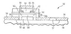
- FIG. 3is a cross-sectional view illustrating one possible configuration of the inventive epitaxial base bipolar transistor that is formed utilizing the first method of the present invention.
- FIG. 4shows a top-down view of the structure shown in FIG. 3 .
- device 50 shown in FIG. 3comprises subcollector (e.g., N+ doped) 52 in a single crystal semiconductor substrate (e.g., N type-Si substrate) 54 containing isolation regions (e.g., shallow trench isolation regions) 56 .
- a base region (e.g. P type) 58 of silicon (epitaxial Si over the silicon substrate, and polysilicon over the isolation regions)is located on top of the substrate surface.
- the basehas regions for forming both intrinsic (P doped) and extrinsic (P+ doped) regions, which are labeled as 58 i and 58 e , respectively.
- the base regionis about 500 to about 3000 ⁇ thick.
- Ge rich layer 60which has a thickness of from about 250 to about 1500 ⁇ located about 50 to about 500 ⁇ from the top of base 58 .
- insulator 62On top of the base region, is insulator 62 having an opening exposing the base region silicon. Overlapping this opening, is polysilicon emitter (N+ doped) region 64 which includes capping layer 65 that is made from an insulator, i.e., dielectric. Some of the doping from the emitter region is diffused into the base region.
- the extrinsic base regionsurrounds the intrinsic base region and the emitter, though it is to a fixed depth no deeper than the Ge rich layer and also surrounds most of the emitter, though it is separated from the emitter by insulator spacers 66 .
- pedestal region 68N+ doped extending from the subcollector into the base region., but not contacting the isolation regions.
- base region 58is a raised base region which extends to the surface of substrate 52 .
- the bipolar transistor of the present inventionincludes a diffusion from the raised emitter and from the raised extrinsic base which provides an emitter diffusion region and an extrinsic base diffusion region in the structure.
- the inventive bipolar transistoris further characterized as having an emitter diffusion region which has an emitter junction depth associated therewith and the emitter extends to the surface of substrate 52 .
- the inventive bipolar deviceis also characterized as having an emitter to base surface height difference that is less than 20% of the emitter junction.
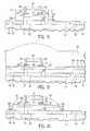
- FIGS. 5-11are pictorial representations through various processing steps of the first method of the present invention which are employed in forming the structure shown in FIG. 3 .
- the first method of the present inventionforms the emitter region prior to forming the extrinsic base.
- FIG. 5illustrates an initial structure 50 employed in the present invention.
- the initial structure shown in FIG. 5comprises a Si substrate 54 containing isolation regions 56 , subcollector 52 , subcollector contact 57 and pedestal region 68 .
- This initial structureis fabricated utilizing conventional process techniques well known in the art; therefore a detailed description of the same is not provided herein.
- a polysilicon intrinsic base layer 58 iis grown epitaxially on the surface of the Si substrate using a chemical vapor deposition (CVD) process.
- the intrinsic base layerhas a thickness of from about 500 to about 3000 ⁇ and is intrinsically doped with a P-type dopant.
- the intrinsic base layer of the present inventionalso includes a Ge rich layer 60 which has the above mentioned thickness located therein.
- a thin oxide layer 59 followed by a thin nitride layer 61are formed on the grown intrinsic base layer.
- the oxide and nitride layerswhich form a dual dielectric layer, are formed utilizing the same or different deposition process including, but not limited to: CVD, plasma-enhanced CVD, chemical solution deposition and other like deposition processes.
- the oxide layerhas a thickness of from about 50 to about 200 ⁇ , whereas the nitride layer has a thickness of from about 100 to about 500 ⁇ . It is also possible in the present invention to utilize an oxide layer that is the same or different from oxide layer 59 in place of nitride layer 61 .
- polysilicon layer 64is formed by conventional deposition processes such as CVD and thereafter the polysilicon layer is doped with an N-type doping utilizing a conventional ion implantation process.
- Layer 65which may be composed of a nitride or oxide is then formed on top of polysilicon layer 63 utilizing a conventional deposition process and thereafter nitride layer 61 and the emitter polysilicon is etched to form the raised emitter region.
- sidewall spacers 66are formed on the emitter by depositing 500-1000 ⁇ nitride and RIE the deposited nitride with a process that is selective to oxide, See FIG. 6 .
- oxide layer 59 not covered by spacers 64is removed by a conventional wet etching process.
- a P+ polysilicon film 70is deposited by conventional in-situ doping deposition processes such as CVD which are capable of depositing polysilicon at low temperatures, i.e., at temperatures of 550° C. or less.
- the P+ polysiliconhas a thickness of from about 5000 to about 30,000 ⁇ and it is highly doped having a dopant concentration on the order of 1 ⁇ 10 19 cm ⁇ 3 or above.
- the P+ polysilicon film used in this step of the present inventionmay or may not contain Ge.
- the low temperature deposition process employed in forming the P+ polysilicon filmreduces dopant diffusion in the existing films; namely the SiGe base layer.
- FIG. 9shows the inventive bipolar structure after the polysilicon layer has been RIE to form polysilicon sidewalls 72 around the emitter region. It is noted that polysilicon sidewalls 72 created in this step of the present invention are used in forming the raised extrinsic base region of the inventive bipolar transistor.
- a conventional photoresist mask 74is formed over the structure so as to define the extrinsic base region and any portion of the exposed base region is removed from the structure by utilizing a conventional etching processes well known in the art exposing the isolation regions. After this etching step, the photoresist mask is removed utilizing a conventional stripping process.
- FIG. 11show the structure after etching and subsequent removal of the photoresist mask.
- the structure of FIG. 11is then subjected to a rapid thermal annealing step which is used to diffuse and activate the N+ doping of the emitter and drive it into the intrinsic base to a fixed depth to the base-emitter junction.
- the annealing stepprovides the structure shown in FIG. 3 .
- the rapid thermal annealing processis carried out in an inert gas atmosphere such as N 2 or Ar at a temperature of greater than about 850° for a time period of less than about 30 seconds.
- the dopantis driven into the intrinsic base region to a depth of from about 50 to about 500 ⁇ below the top surface of the intrinsic base region.
- the annealing processalso drives in the P+ boron dopant from the extrinsic base into the intrinsic base.
- the extrinsic base outdiffusion from the P+ polysiliconnow contacts on the in-situ doped boron from the intrinsic base. Since ion implantation is not employed in the present invention in forming the extrinsic base region, no transient enhanced diffusion of dopants occurs; therefore decreasing the capacitance of the bipolar transistor.
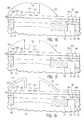
- FIGS. 12-13describe an alternative embodiment of the first method of the present invention which differs from above mentioned processing steps after the processing leading up to the structure of FIG. 8 are first performed, i.e., deposition of the extrinsic base polysilicon has been completed.
- a spacer RIE processis performed to form superspacer 80 shown in FIG. 13 .
- the superspaceris formed by first depositing a P+ dielectric material 80 on the structure shown in FIG., 8 so as to form the structure shown in FIG. 12 and thereafter selectively etching the dielectric material and portions of the base region. This saves the additional masking step as in FIG. 10 .
- the spacer etchis followed by a rapid thermal anneal to drive dopants down threw the emitter and base regions as described in the first embodiment.
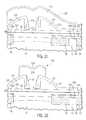
- FIGS. 14-26are pictorial representations illustrating the second method of the present invention.
- the second method of the present inventionforms the extrinsic base prior to forming the emitter region.
- the bipolar transistorincludes an emitter region that is self-aligned and centered to the base region.
- FIG. 14illustrates an initial structure employed in the second method of the present invention.
- the initial structure shown in FIG. 14includes an epitaxial/polysilicon base layer 58 containing embedded Ge rich layer 60 , formed on the surface of substrate 54 .
- the substrateincludes subcollector region 52 , subcollector contact 57 and isolation regions 56 .
- the isolation regionsare protected by oxide layer 108 and nitride layer 106 .
- the structure shown in FIG. 14is fabricated utilizing processing techniques that are well known to those skilled in the art; therefore a description concerning the same is not provided herein.
- mandrel 110formed from layers of oxide 112 , silicon nitride 114 , and a layer of tetraethylortosilicate (TEOS) 116 , respectively.
- the mandrelis formed by sequentially depositing each of the above mentioned layers and thereafter the deposited mandrel layers are patterned by conventional lithography and etching.
- the thicknesses of the individual layers that form the mandrelmay vary and are not important to the present invention.
- FIG. 15shows the formation of a layer of in-situ doped P+ polysilicon 118 on the structure.
- This in-situ doped layeris formed by conventional processes and it typically has a thickness of at least 1000 ⁇ .
- FIG. 16shows the structure after a RIE process has been performed to form wide superspacers 120 .
- the RIE process employed in this step of the present inventionis designed to be selective to polysilicon over oxide.
- TEOS layer 116is selectively etched stopping on nitride layer 114 by utilizing a conventional wet etch process forming trench 115 in the structure.
- FIG. 18shows the structure after a layer of oxide 122 having a thickness of from about 700 to about 1000 ⁇ has been formed over the P+ polysilicon layer. This oxide layer is typically formed by utilizing a high pressure oxidation process.
- FIG. 19shows the structure after depositing silicon nitride layer 124 and etching this silicon nitride layer by a spacer RIE process selective to oxide to form nitride spacers 124 on the structure. It should be noted that during this step of the second method of the present invention the silicon nitride present in the bottom of the trench is removed.
- FIG. 21shows the structure after a thick layer (on the order of 1500 ⁇ or greater) of N+ (As) doped polysilicon 126 has been deposited followed by the formation of a thin silicon nitride cap layer 128 .
- emitter 130is now formed by etching portions of the silicon nitride cap and the N+ doped polysilicon layer formed in FIG. 21 .
- the etching step used in the step of the inventionis selective for the above materials and it stops on the oxide layer grown in FIG. 18 .
- a layer of silicon nitride having a thickness of about 200 to about 500 ⁇is deposited by conventional means and a RIE process selective to oxide is performed to produce nitride spacers 132 on the exposed surface of the emitter region. The above steps are illustrated in FIG. 23 .
- FIG. 24shows the structure after a portion of oxide layer 122 has been removed therefrom utilizing a conventional etching process such as RIE.
- RIEetching process
- photoresistis deposited and patterned by lithography providing patterned photoresist 134 .
- a RIE processis thereafter employed to define the extrinsic base region. This is followed by a rapid thermal anneal process which is capable of forming the emitter base and driving down the emitter.
- FIG. 26shows the structure after a conventional silicide process is employed so as to form silicide regions 136 in the structure.
- bipolar structures of the present inventionregardless of which method is used in fabricating the same, have a lower collector base capacitance than previous prior art structures and a higher f t as the pedestal may be doped higher; therefore higher f max may be achieved.
- the present inventionalso provides a bipolar junction transistor which has resistance/capacitance control built therein.
- the inventive bipolar junction transistorincludes a bipolar junction transistor comprising a self-aligned base/emitter structure wherein a base-resistance is independently controlled by a diffusion source of variable thickness, and wherein the base-capacitance is independently variable due to the combination of the thickness of the diffusion source and a thickness of an intrinsic base epitaxial layer.
- the extrinsic base-collector capacitance (shown schematically as capacitors in FIG. 3) between the p+ diffusion source ( 72 in FIG. 11) and the selectively implanted collector ( 68 in FIG. 3)can be modulated by either thickening the epitaxial base region (layer 58 in FIG. 3) or by shallowing the diffusion of p+ dopants from the p+ diffusion source. Since the inventors have independent control of these two variables, the inventors can reduce the base-collector capacitance to increase device performance.
- the thickness of the epitaxial base regionis limited by other process constraints (such as selective epitaxy) that do not allow the ability to modulate the base-collector capacitance as in this disclosure.
Landscapes
- Bipolar Transistors (AREA)
Abstract
Description
Claims (7)
Priority Applications (1)
| Application Number | Priority Date | Filing Date | Title |
|---|---|---|---|
| US10/425,270US6812545B2 (en) | 2001-03-16 | 2003-04-29 | Epitaxial base bipolar transistor with raised extrinsic base |
Applications Claiming Priority (2)
| Application Number | Priority Date | Filing Date | Title |
|---|---|---|---|
| US09/810,856US6617220B2 (en) | 2001-03-16 | 2001-03-16 | Method for fabricating an epitaxial base bipolar transistor with raised extrinsic base |
| US10/425,270US6812545B2 (en) | 2001-03-16 | 2003-04-29 | Epitaxial base bipolar transistor with raised extrinsic base |
Related Parent Applications (1)
| Application Number | Title | Priority Date | Filing Date |
|---|---|---|---|
| US09/810,856DivisionUS6617220B2 (en) | 2001-03-16 | 2001-03-16 | Method for fabricating an epitaxial base bipolar transistor with raised extrinsic base |
Publications (2)
| Publication Number | Publication Date |
|---|---|
| US20030201517A1 US20030201517A1 (en) | 2003-10-30 |
| US6812545B2true US6812545B2 (en) | 2004-11-02 |
Family
ID=25204888
Family Applications (2)
| Application Number | Title | Priority Date | Filing Date |
|---|---|---|---|
| US09/810,856Expired - LifetimeUS6617220B2 (en) | 2001-03-16 | 2001-03-16 | Method for fabricating an epitaxial base bipolar transistor with raised extrinsic base |
| US10/425,270Expired - LifetimeUS6812545B2 (en) | 2001-03-16 | 2003-04-29 | Epitaxial base bipolar transistor with raised extrinsic base |
Family Applications Before (1)
| Application Number | Title | Priority Date | Filing Date |
|---|---|---|---|
| US09/810,856Expired - LifetimeUS6617220B2 (en) | 2001-03-16 | 2001-03-16 | Method for fabricating an epitaxial base bipolar transistor with raised extrinsic base |
Country Status (2)
| Country | Link |
|---|---|
| US (2) | US6617220B2 (en) |
| JP (1) | JP2002313798A (en) |
Cited By (14)
| Publication number | Priority date | Publication date | Assignee | Title |
|---|---|---|---|---|
| US20050024933A1 (en)* | 2003-05-07 | 2005-02-03 | Stmicroelectronics S.R.L. | Process for manufacturing device having selector transistors for storage elements and memory device fabricated thereby |
| US20050164454A1 (en)* | 2004-01-27 | 2005-07-28 | Micron Technology, Inc. | Selective epitaxy vertical integrated circuit components and methods |
| US20080078997A1 (en)* | 2005-07-06 | 2008-04-03 | Khater Marwan H | Method for forming a bipolar transistor device with self-aligned raised extrinsic base |
| US7863133B2 (en) | 2005-06-28 | 2011-01-04 | Micron Technology, Inc. | Oxide epitaxial isolation |
| US20130168821A1 (en)* | 2012-01-04 | 2013-07-04 | International Business Machines Corporation | Soi lateral bipolar transistor having multi-sided base contact and methods for making same |
| US8526220B2 (en) | 2011-06-12 | 2013-09-03 | International Business Machines Corporation | Complementary SOI lateral bipolar for SRAM in a low-voltage CMOS platform |
| US8531001B2 (en) | 2011-06-12 | 2013-09-10 | International Business Machines Corporation | Complementary bipolar inverter |
| US8536012B2 (en) | 2011-07-06 | 2013-09-17 | International Business Machines Corporation | Bipolar junction transistors with a link region connecting the intrinsic and extrinsic bases |
| US8796149B1 (en) | 2013-02-18 | 2014-08-05 | International Business Machines Corporation | Collector-up bipolar junction transistors in BiCMOS technology |
| US8917547B2 (en) | 2012-12-02 | 2014-12-23 | International Business Machines Corporation | Complementary SOI lateral bipolar for SRAM in a CMOS platform |
| US8916446B2 (en) | 2011-11-11 | 2014-12-23 | International Business Machines Corporation | Bipolar junction transistor with multiple emitter fingers |
| US8956945B2 (en) | 2013-02-04 | 2015-02-17 | International Business Machines Corporation | Trench isolation for bipolar junction transistors in BiCMOS technology |
| US9059138B2 (en) | 2012-01-25 | 2015-06-16 | International Business Machines Corporation | Heterojunction bipolar transistor with reduced sub-collector length, method of manufacture and design structure |
| US9093491B2 (en) | 2012-12-05 | 2015-07-28 | International Business Machines Corporation | Bipolar junction transistors with reduced base-collector junction capacitance |
Families Citing this family (30)
| Publication number | Priority date | Publication date | Assignee | Title |
|---|---|---|---|---|
| US6700818B2 (en) | 2002-01-31 | 2004-03-02 | Saifun Semiconductors Ltd. | Method for operating a memory device |
| US6975536B2 (en)* | 2002-01-31 | 2005-12-13 | Saifun Semiconductors Ltd. | Mass storage array and methods for operation thereof |
| US6767798B2 (en)* | 2002-04-09 | 2004-07-27 | Maxim Integrated Products, Inc. | Method of forming self-aligned NPN transistor with raised extrinsic base |
| US6936519B2 (en)* | 2002-08-19 | 2005-08-30 | Chartered Semiconductor Manufacturing, Ltd. | Double polysilicon bipolar transistor and method of manufacture therefor |
| US6962842B1 (en) | 2003-03-06 | 2005-11-08 | Maxim Integrated Products, Inc. | Method of removing a sacrificial emitter feature in a BICMOS process with a super self-aligned BJT |
| KR100518561B1 (en)* | 2003-03-06 | 2005-10-04 | 삼성전자주식회사 | Method for manufacturing bipolar device including germane gas pre-treatment on single crystalline silicon layer and apparatus by the same |
| KR100546332B1 (en)* | 2003-06-13 | 2006-01-26 | 삼성전자주식회사 | Bipolar junction transistor and method of manufacturing the same |
| TWI241025B (en)* | 2003-06-13 | 2005-10-01 | Samsung Electronics Co Ltd | Bipolar junction transistors and methods of manufacturing the same |
| FR2858877B1 (en)* | 2003-08-11 | 2005-10-21 | St Microelectronics Sa | BIPOLAR TRANSISTOR WITH HETEROJUNCTION |
| US7005359B2 (en)* | 2003-11-17 | 2006-02-28 | Intel Corporation | Bipolar junction transistor with improved extrinsic base region and method of fabrication |
| US6869852B1 (en) | 2004-01-09 | 2005-03-22 | International Business Machines Corporation | Self-aligned raised extrinsic base bipolar transistor structure and method |
| US7037798B2 (en) | 2004-01-09 | 2006-05-02 | International Business Machines Corporation | Bipolar transistor structure with self-aligned raised extrinsic base and methods |
| EP1733430A1 (en)* | 2004-03-10 | 2006-12-20 | Agere Systems, Inc. | A bipolar junction transistor having a high germanium concentration in a silicon-germanium layer and a method for forming the bipolar junction transistor |
| TW200620478A (en)* | 2004-08-20 | 2006-06-16 | Koninkl Philips Electronics Nv | Self-aligned epitaxially grown bipolar transistor |
| US7265018B2 (en)* | 2004-09-21 | 2007-09-04 | International Business Machines Corporation | Method to build self-aligned NPN in advanced BiCMOS technology |
| US7262484B2 (en)* | 2005-05-09 | 2007-08-28 | International Business Machines Corporation | Structure and method for performance improvement in vertical bipolar transistors |
| US20070023864A1 (en)* | 2005-07-28 | 2007-02-01 | International Business Machines Corporation | Methods of fabricating bipolar transistor for improved isolation, passivation and critical dimension control |
| US7342293B2 (en)* | 2005-12-05 | 2008-03-11 | International Business Machines Corporation | Bipolar junction transistors (BJTS) with second shallow trench isolation (STI) regions, and methods for forming same |
| JP2007250903A (en) | 2006-03-16 | 2007-09-27 | Matsushita Electric Ind Co Ltd | Heterojunction bipolar transistor and manufacturing method thereof |
| US7772060B2 (en)* | 2006-06-21 | 2010-08-10 | Texas Instruments Deutschland Gmbh | Integrated SiGe NMOS and PMOS transistors |
| US20080217742A1 (en)* | 2007-03-09 | 2008-09-11 | International Business Machines Corporation | Tailored bipolar transistor doping profile for improved reliability |
| US8020128B2 (en) | 2009-06-29 | 2011-09-13 | International Business Machines Corporation | Scaling of bipolar transistors |
| US10011920B2 (en) | 2011-02-23 | 2018-07-03 | International Business Machines Corporation | Low-temperature selective epitaxial growth of silicon for device integration |
| US8921194B2 (en) | 2011-11-11 | 2014-12-30 | International Business Machines Corporation | PNP bipolar junction transistor fabrication using selective epitaxy |
| CN102569069B (en)* | 2012-03-09 | 2014-08-27 | 中国科学院上海微系统与信息技术研究所 | SiGe-heterojunction bipolar transistor (HBT) and preparation method thereof |
| US9059212B2 (en) | 2012-10-31 | 2015-06-16 | International Business Machines Corporation | Back-end transistors with highly doped low-temperature contacts |
| US8785977B2 (en)* | 2012-11-08 | 2014-07-22 | Shanghai Hua Hong Nec Electronics Co., Ltd. | High speed SiGe HBT and manufacturing method thereof |
| US8912071B2 (en)* | 2012-12-06 | 2014-12-16 | International Business Machines Corporation | Selective emitter photovoltaic device |
| US11276682B1 (en)* | 2020-09-01 | 2022-03-15 | Newport Fab, Llc | Nickel silicide in bipolar complementary-metal-oxide-semiconductor (BiCMOS) device and method of manufacturing |
| US11588043B2 (en) | 2021-04-14 | 2023-02-21 | Globalfoundries U.S. Inc. | Bipolar transistor with elevated extrinsic base and methods to form same |
Citations (25)
| Publication number | Priority date | Publication date | Assignee | Title |
|---|---|---|---|---|
| US4319932A (en) | 1980-03-24 | 1982-03-16 | International Business Machines Corporation | Method of making high performance bipolar transistor with polysilicon base contacts |
| US4338138A (en) | 1980-03-03 | 1982-07-06 | International Business Machines Corporation | Process for fabricating a bipolar transistor |
| US4682409A (en) | 1985-06-21 | 1987-07-28 | Advanced Micro Devices, Inc. | Fast bipolar transistor for integrated circuit structure and method for forming same |
| US4799099A (en) | 1986-01-30 | 1989-01-17 | Texas Instruments Incorporated | Bipolar transistor in isolation well with angled corners |
| US4839305A (en) | 1988-06-28 | 1989-06-13 | Texas Instruments Incorporated | Method of making single polysilicon self-aligned transistor |
| US4960726A (en) | 1989-10-19 | 1990-10-02 | International Business Machines Corporation | BiCMOS process |
| US5008207A (en) | 1989-09-11 | 1991-04-16 | International Business Machines Corporation | Method of fabricating a narrow base transistor |
| US5017990A (en) | 1989-12-01 | 1991-05-21 | International Business Machines Corporation | Raised base bipolar transistor structure and its method of fabrication |
| US5101256A (en) | 1989-02-13 | 1992-03-31 | International Business Machines Corporation | Bipolar transistor with ultra-thin epitaxial base and method of fabricating same |
| US5117271A (en) | 1990-12-07 | 1992-05-26 | International Business Machines Corporation | Low capacitance bipolar junction transistor and fabrication process therfor |
| US5175607A (en) | 1990-04-26 | 1992-12-29 | Mitsubishi Denki Kabushiki Kaisha | Semiconductor device and manufacturing method thereof |
| US5194926A (en) | 1991-10-03 | 1993-03-16 | Motorola Inc. | Semiconductor device having an inverse-T bipolar transistor |
| US5217909A (en)* | 1990-07-18 | 1993-06-08 | Siemens Aktiengesellschaft | Method for manufacturing a bipolar transistor |
| US5298786A (en) | 1990-12-06 | 1994-03-29 | International Business Machines Corp. | SOI lateral bipolar transistor with edge-strapped base contact and method of fabricating same |
| US5488002A (en) | 1993-09-10 | 1996-01-30 | Kabushiki Kaisha Toshiba | Method for manufacturing self-aligned bipolar transistors using double diffusion |
| US5523245A (en) | 1994-05-12 | 1996-06-04 | Nec Corporation | Process for fabricating high-performance facet-free small-sized bipolar transistor |
| US5525818A (en) | 1992-08-31 | 1996-06-11 | Texas Instruments Incorporated | Reducing extrinsic base-collector capacitance |
| US5541120A (en)* | 1992-01-31 | 1996-07-30 | Analog Devices, Inc. | Method of making complementary bipolar polysilicon emitter devices |
| US5557131A (en) | 1992-10-19 | 1996-09-17 | At&T Global Information Solutions Company | Elevated emitter for double poly BICMOS devices |
| US5773350A (en) | 1997-01-28 | 1998-06-30 | National Semiconductor Corporation | Method for forming a self-aligned bipolar junction transistor with silicide extrinsic base contacts and selective epitaxial grown intrinsic base |
| US5925923A (en) | 1997-02-20 | 1999-07-20 | National Semiconductor Corporation | Merged single polysilicon bipolar NPN transistor |
| US6020246A (en) | 1998-03-13 | 2000-02-01 | National Semiconductor Corporation | Forming a self-aligned epitaxial base bipolar transistor |
| US6054358A (en)* | 1997-08-20 | 2000-04-25 | Nec Corporation | Semiconductor device and manufacturing method of the same |
| US6265276B1 (en) | 1994-07-12 | 2001-07-24 | Sony Corporation | Structure and fabrication of bipolar transistor |
| US6365451B2 (en) | 1997-12-17 | 2002-04-02 | Texas Instruments Incorporated | Transistor and method |
Family Cites Families (5)
| Publication number | Priority date | Publication date | Assignee | Title |
|---|---|---|---|---|
| US4927774A (en)* | 1988-06-10 | 1990-05-22 | British Telecommunications Plc | Self aligned bipolar fabrication process |
| US5162245A (en)* | 1988-06-28 | 1992-11-10 | Texas Instruments Incorporated | Self-aligned bipolar transistor using selective polysilicon growth |
| US5213989A (en)* | 1992-06-24 | 1993-05-25 | Motorola, Inc. | Method for forming a grown bipolar electrode contact using a sidewall seed |
| FR2804247B1 (en)* | 2000-01-21 | 2002-04-12 | St Microelectronics Sa | METHOD FOR PRODUCING A BIPOLAR TRANSISTOR WITH SELF-ALIGNED EXTRINSIC BASE |
| US6534372B1 (en)* | 2000-11-22 | 2003-03-18 | Newport Fab, Llc | Method for fabricating a self-aligned emitter in a bipolar transistor |
- 2001
- 2001-03-16USUS09/810,856patent/US6617220B2/ennot_activeExpired - Lifetime
- 2002
- 2002-02-27JPJP2002052091Apatent/JP2002313798A/enactivePending
- 2003
- 2003-04-29USUS10/425,270patent/US6812545B2/ennot_activeExpired - Lifetime
Patent Citations (25)
| Publication number | Priority date | Publication date | Assignee | Title |
|---|---|---|---|---|
| US4338138A (en) | 1980-03-03 | 1982-07-06 | International Business Machines Corporation | Process for fabricating a bipolar transistor |
| US4319932A (en) | 1980-03-24 | 1982-03-16 | International Business Machines Corporation | Method of making high performance bipolar transistor with polysilicon base contacts |
| US4682409A (en) | 1985-06-21 | 1987-07-28 | Advanced Micro Devices, Inc. | Fast bipolar transistor for integrated circuit structure and method for forming same |
| US4799099A (en) | 1986-01-30 | 1989-01-17 | Texas Instruments Incorporated | Bipolar transistor in isolation well with angled corners |
| US4839305A (en) | 1988-06-28 | 1989-06-13 | Texas Instruments Incorporated | Method of making single polysilicon self-aligned transistor |
| US5101256A (en) | 1989-02-13 | 1992-03-31 | International Business Machines Corporation | Bipolar transistor with ultra-thin epitaxial base and method of fabricating same |
| US5008207A (en) | 1989-09-11 | 1991-04-16 | International Business Machines Corporation | Method of fabricating a narrow base transistor |
| US4960726A (en) | 1989-10-19 | 1990-10-02 | International Business Machines Corporation | BiCMOS process |
| US5017990A (en) | 1989-12-01 | 1991-05-21 | International Business Machines Corporation | Raised base bipolar transistor structure and its method of fabrication |
| US5175607A (en) | 1990-04-26 | 1992-12-29 | Mitsubishi Denki Kabushiki Kaisha | Semiconductor device and manufacturing method thereof |
| US5217909A (en)* | 1990-07-18 | 1993-06-08 | Siemens Aktiengesellschaft | Method for manufacturing a bipolar transistor |
| US5298786A (en) | 1990-12-06 | 1994-03-29 | International Business Machines Corp. | SOI lateral bipolar transistor with edge-strapped base contact and method of fabricating same |
| US5117271A (en) | 1990-12-07 | 1992-05-26 | International Business Machines Corporation | Low capacitance bipolar junction transistor and fabrication process therfor |
| US5194926A (en) | 1991-10-03 | 1993-03-16 | Motorola Inc. | Semiconductor device having an inverse-T bipolar transistor |
| US5541120A (en)* | 1992-01-31 | 1996-07-30 | Analog Devices, Inc. | Method of making complementary bipolar polysilicon emitter devices |
| US5525818A (en) | 1992-08-31 | 1996-06-11 | Texas Instruments Incorporated | Reducing extrinsic base-collector capacitance |
| US5557131A (en) | 1992-10-19 | 1996-09-17 | At&T Global Information Solutions Company | Elevated emitter for double poly BICMOS devices |
| US5488002A (en) | 1993-09-10 | 1996-01-30 | Kabushiki Kaisha Toshiba | Method for manufacturing self-aligned bipolar transistors using double diffusion |
| US5523245A (en) | 1994-05-12 | 1996-06-04 | Nec Corporation | Process for fabricating high-performance facet-free small-sized bipolar transistor |
| US6265276B1 (en) | 1994-07-12 | 2001-07-24 | Sony Corporation | Structure and fabrication of bipolar transistor |
| US5773350A (en) | 1997-01-28 | 1998-06-30 | National Semiconductor Corporation | Method for forming a self-aligned bipolar junction transistor with silicide extrinsic base contacts and selective epitaxial grown intrinsic base |
| US5925923A (en) | 1997-02-20 | 1999-07-20 | National Semiconductor Corporation | Merged single polysilicon bipolar NPN transistor |
| US6054358A (en)* | 1997-08-20 | 2000-04-25 | Nec Corporation | Semiconductor device and manufacturing method of the same |
| US6365451B2 (en) | 1997-12-17 | 2002-04-02 | Texas Instruments Incorporated | Transistor and method |
| US6020246A (en) | 1998-03-13 | 2000-02-01 | National Semiconductor Corporation | Forming a self-aligned epitaxial base bipolar transistor |
Non-Patent Citations (5)
| Title |
|---|
| "Bipolar Transistor With Pedestal Subcollector Regions Self-Aligned Underneath Field Oxide Eegions", IBM Technical Disclosure Bulletin, pp. 252-253, Aug. 1988. |
| "Fabricating Pedestal Transistor", IBM Technical Disclosure Bulletin, pp. 179-180, Jun. 1971. |
| "Lateral Bipolar Transistor With Elevated Base Contact", IBM Technical Disclosure Bulletin, pp. 157-159, Nov. 1989. |
| Abstract of Japanese Patent No. 04207038 A, issued Nov. 30, 1990. |
| Abstract of Japanese Patent No. 09069528 A, issued Mar. 11, 1995. |
Cited By (28)
| Publication number | Priority date | Publication date | Assignee | Title |
|---|---|---|---|---|
| US20050024933A1 (en)* | 2003-05-07 | 2005-02-03 | Stmicroelectronics S.R.L. | Process for manufacturing device having selector transistors for storage elements and memory device fabricated thereby |
| US20050164454A1 (en)* | 2004-01-27 | 2005-07-28 | Micron Technology, Inc. | Selective epitaxy vertical integrated circuit components and methods |
| US20060006444A1 (en)* | 2004-01-27 | 2006-01-12 | Micron Technology, Inc. | Selective epitaxy vertical integrated circuit components and methods |
| US7372091B2 (en) | 2004-01-27 | 2008-05-13 | Micron Technology, Inc. | Selective epitaxy vertical integrated circuit components |
| US7514324B2 (en) | 2004-01-27 | 2009-04-07 | Micron Technology, Inc. | Selective epitaxy in vertical integrated circuit |
| US20090197379A1 (en)* | 2004-01-27 | 2009-08-06 | Leslie Terrence C | Selective epitaxy vertical integrated circuit components and methods |
| US7851309B2 (en) | 2004-01-27 | 2010-12-14 | Micron Technology, Inc. | Selective epitaxy vertical integrated circuit components and methods |
| US7863133B2 (en) | 2005-06-28 | 2011-01-04 | Micron Technology, Inc. | Oxide epitaxial isolation |
| US20080078997A1 (en)* | 2005-07-06 | 2008-04-03 | Khater Marwan H | Method for forming a bipolar transistor device with self-aligned raised extrinsic base |
| US7935986B2 (en) | 2005-07-06 | 2011-05-03 | International Business Machines Corporation | Method for forming a bipolar transistor device with self-aligned raised extrinsic base |
| US8847348B2 (en) | 2011-06-12 | 2014-09-30 | International Business Machines Corporation | Complementary bipolar inverter |
| US8526220B2 (en) | 2011-06-12 | 2013-09-03 | International Business Machines Corporation | Complementary SOI lateral bipolar for SRAM in a low-voltage CMOS platform |
| US8531001B2 (en) | 2011-06-12 | 2013-09-10 | International Business Machines Corporation | Complementary bipolar inverter |
| US8716837B2 (en) | 2011-07-06 | 2014-05-06 | International Business Machines Corporation | Bipolar junction transistors with a link region connecting the intrinsic and extrinsic bases |
| US8536012B2 (en) | 2011-07-06 | 2013-09-17 | International Business Machines Corporation | Bipolar junction transistors with a link region connecting the intrinsic and extrinsic bases |
| US8916446B2 (en) | 2011-11-11 | 2014-12-23 | International Business Machines Corporation | Bipolar junction transistor with multiple emitter fingers |
| US9159801B2 (en) | 2011-11-11 | 2015-10-13 | GlobalFoundries, Inc. | Bipolar junction transistor with multiple emitter fingers |
| US9293454B2 (en) | 2012-01-04 | 2016-03-22 | Globalfoundries Inc. | Bipolar junction transistor having multi-sided base contact |
| US20130168821A1 (en)* | 2012-01-04 | 2013-07-04 | International Business Machines Corporation | Soi lateral bipolar transistor having multi-sided base contact and methods for making same |
| US8946040B2 (en)* | 2012-01-04 | 2015-02-03 | International Business Machines Corporation | SOI lateral bipolar transistor having multi-sided base contact and methods for making same |
| US9059138B2 (en) | 2012-01-25 | 2015-06-16 | International Business Machines Corporation | Heterojunction bipolar transistor with reduced sub-collector length, method of manufacture and design structure |
| US8917547B2 (en) | 2012-12-02 | 2014-12-23 | International Business Machines Corporation | Complementary SOI lateral bipolar for SRAM in a CMOS platform |
| US8929133B2 (en) | 2012-12-02 | 2015-01-06 | International Business Machines Corporation | Complementary SOI lateral bipolar for SRAM in a CMOS platform |
| US9093491B2 (en) | 2012-12-05 | 2015-07-28 | International Business Machines Corporation | Bipolar junction transistors with reduced base-collector junction capacitance |
| US9240448B2 (en) | 2012-12-05 | 2016-01-19 | Globalfoundries Inc. | Bipolar junction transistors with reduced base-collector junction capacitance |
| US8956945B2 (en) | 2013-02-04 | 2015-02-17 | International Business Machines Corporation | Trench isolation for bipolar junction transistors in BiCMOS technology |
| US9337323B2 (en) | 2013-02-04 | 2016-05-10 | Globalfoundries Inc. | Trench isolation for bipolar junction transistors in BiCMOS technology |
| US8796149B1 (en) | 2013-02-18 | 2014-08-05 | International Business Machines Corporation | Collector-up bipolar junction transistors in BiCMOS technology |
Also Published As
| Publication number | Publication date |
|---|---|
| JP2002313798A (en) | 2002-10-25 |
| US6617220B2 (en) | 2003-09-09 |
| US20030201517A1 (en) | 2003-10-30 |
| US20020132438A1 (en) | 2002-09-19 |
Similar Documents
| Publication | Publication Date | Title |
|---|---|---|
| US6812545B2 (en) | Epitaxial base bipolar transistor with raised extrinsic base | |
| US6900519B2 (en) | Diffused extrinsic base and method for fabrication | |
| US5024957A (en) | Method of fabricating a bipolar transistor with ultra-thin epitaxial base | |
| US5101256A (en) | Bipolar transistor with ultra-thin epitaxial base and method of fabricating same | |
| US4839305A (en) | Method of making single polysilicon self-aligned transistor | |
| US6989557B2 (en) | Bipolar junction transistor and fabricating method | |
| US20150140771A1 (en) | Method for fabricating a bipolar transistor having self-aligned emitter contact | |
| KR100205017B1 (en) | Manufacturing method of heterojunction bipolar transistor | |
| US6794237B2 (en) | Lateral heterojunction bipolar transistor | |
| JPH04264735A (en) | Vertical bipolar transistor provided with u-shaped epitaxially grown peculiar region and its manufacture | |
| US7105415B2 (en) | Method for the production of a bipolar transistor | |
| US6913981B2 (en) | Method of fabricating a bipolar transistor using selective epitaxially grown SiGe base layer | |
| US6319786B1 (en) | Self-aligned bipolar transistor manufacturing method | |
| JPH0646638B2 (en) | Vertical bipolar transistor and method of manufacturing the same | |
| US6699741B1 (en) | Single poly bipolar transistor and method that uses a selectively epitaxially grown highly-boron-doped silicon layer as a diffusion source for an extrinsic base region | |
| US20020197807A1 (en) | Non-self-aligned SiGe heterojunction bipolar transistor | |
| JPH10326793A (en) | Method for manufacturing semiconductor device | |
| US5523614A (en) | Bipolar transistor having enhanced high speed operation through reduced base leakage current | |
| JP3332037B2 (en) | Method for defining two self-aligned regions on the upper surface of a substrate | |
| JP3456864B2 (en) | Semiconductor device and manufacturing method thereof | |
| US5175117A (en) | Method for making buried isolation | |
| US6696342B1 (en) | Small emitter and base-collector bi-polar transistor | |
| JP3908023B2 (en) | Manufacturing method of semiconductor device | |
| KR100422360B1 (en) | Bipolar transistor and fabricating method thereof | |
| US20060006416A1 (en) | Bipolar transistor with nonselective epitaxial base and raised extrinsic base |
Legal Events
| Date | Code | Title | Description |
|---|---|---|---|
| FEPP | Fee payment procedure | Free format text:PAYOR NUMBER ASSIGNED (ORIGINAL EVENT CODE: ASPN); ENTITY STATUS OF PATENT OWNER: LARGE ENTITY | |
| STCF | Information on status: patent grant | Free format text:PATENTED CASE | |
| FPAY | Fee payment | Year of fee payment:4 | |
| REMI | Maintenance fee reminder mailed | ||
| FPAY | Fee payment | Year of fee payment:8 | |
| SULP | Surcharge for late payment | Year of fee payment:7 | |
| AS | Assignment | Owner name:GLOBALFOUNDRIES U.S. 2 LLC, NEW YORK Free format text:ASSIGNMENT OF ASSIGNORS INTEREST;ASSIGNOR:INTERNATIONAL BUSINESS MACHINES CORPORATION;REEL/FRAME:036550/0001 Effective date:20150629 | |
| AS | Assignment | Owner name:GLOBALFOUNDRIES INC., CAYMAN ISLANDS Free format text:ASSIGNMENT OF ASSIGNORS INTEREST;ASSIGNORS:GLOBALFOUNDRIES U.S. 2 LLC;GLOBALFOUNDRIES U.S. INC.;REEL/FRAME:036779/0001 Effective date:20150910 | |
| FPAY | Fee payment | Year of fee payment:12 | |
| AS | Assignment | Owner name:WILMINGTON TRUST, NATIONAL ASSOCIATION, DELAWARE Free format text:SECURITY AGREEMENT;ASSIGNOR:GLOBALFOUNDRIES INC.;REEL/FRAME:049490/0001 Effective date:20181127 | |
| AS | Assignment | Owner name:GLOBALFOUNDRIES U.S. INC., CALIFORNIA Free format text:ASSIGNMENT OF ASSIGNORS INTEREST;ASSIGNOR:GLOBALFOUNDRIES INC.;REEL/FRAME:054633/0001 Effective date:20201022 | |
| AS | Assignment | Owner name:GLOBALFOUNDRIES INC., CAYMAN ISLANDS Free format text:RELEASE BY SECURED PARTY;ASSIGNOR:WILMINGTON TRUST, NATIONAL ASSOCIATION;REEL/FRAME:054636/0001 Effective date:20201117 | |
| AS | Assignment | Owner name:GLOBALFOUNDRIES U.S. INC., NEW YORK Free format text:RELEASE BY SECURED PARTY;ASSIGNOR:WILMINGTON TRUST, NATIONAL ASSOCIATION;REEL/FRAME:056987/0001 Effective date:20201117 |