US6811440B1 - Power connector - Google Patents
Power connectorDownload PDFInfo
- Publication number
- US6811440B1 US6811440B1US10/652,956US65295603AUS6811440B1US 6811440 B1US6811440 B1US 6811440B1US 65295603 AUS65295603 AUS 65295603AUS 6811440 B1US6811440 B1US 6811440B1
- Authority
- US
- United States
- Prior art keywords
- connector
- wafer
- edge
- conductive paths
- electrical
- Prior art date
- Legal status (The legal status is an assumption and is not a legal conclusion. Google has not performed a legal analysis and makes no representation as to the accuracy of the status listed.)
- Expired - Lifetime
Links
- 235000012431wafersNutrition0.000claimsdescription69
- 230000013011matingEffects0.000claimsdescription10
- RYGMFSIKBFXOCR-UHFFFAOYSA-NCopperChemical compound[Cu]RYGMFSIKBFXOCR-UHFFFAOYSA-N0.000description1
- 230000005540biological transmissionEffects0.000description1
- 238000010276constructionMethods0.000description1
- 229910052802copperInorganic materials0.000description1
- 239000010949copperSubstances0.000description1
- 238000010438heat treatmentMethods0.000description1
- 239000000463materialSubstances0.000description1
- 230000004048modificationEffects0.000description1
- 238000012986modificationMethods0.000description1
- 230000008054signal transmissionEffects0.000description1
Images


Classifications
- H—ELECTRICITY
- H01—ELECTRIC ELEMENTS
- H01R—ELECTRICALLY-CONDUCTIVE CONNECTIONS; STRUCTURAL ASSOCIATIONS OF A PLURALITY OF MUTUALLY-INSULATED ELECTRICAL CONNECTING ELEMENTS; COUPLING DEVICES; CURRENT COLLECTORS
- H01R12/00—Structural associations of a plurality of mutually-insulated electrical connecting elements, specially adapted for printed circuits, e.g. printed circuit boards [PCB], flat or ribbon cables, or like generally planar structures, e.g. terminal strips, terminal blocks; Coupling devices specially adapted for printed circuits, flat or ribbon cables, or like generally planar structures; Terminals specially adapted for contact with, or insertion into, printed circuits, flat or ribbon cables, or like generally planar structures
- H01R12/70—Coupling devices
- H01R12/7088—Arrangements for power supply
- H—ELECTRICITY
- H01—ELECTRIC ELEMENTS
- H01R—ELECTRICALLY-CONDUCTIVE CONNECTIONS; STRUCTURAL ASSOCIATIONS OF A PLURALITY OF MUTUALLY-INSULATED ELECTRICAL CONNECTING ELEMENTS; COUPLING DEVICES; CURRENT COLLECTORS
- H01R12/00—Structural associations of a plurality of mutually-insulated electrical connecting elements, specially adapted for printed circuits, e.g. printed circuit boards [PCB], flat or ribbon cables, or like generally planar structures, e.g. terminal strips, terminal blocks; Coupling devices specially adapted for printed circuits, flat or ribbon cables, or like generally planar structures; Terminals specially adapted for contact with, or insertion into, printed circuits, flat or ribbon cables, or like generally planar structures
- H01R12/70—Coupling devices
- H01R12/71—Coupling devices for rigid printing circuits or like structures
- H01R12/72—Coupling devices for rigid printing circuits or like structures coupling with the edge of the rigid printed circuits or like structures
- H01R12/722—Coupling devices for rigid printing circuits or like structures coupling with the edge of the rigid printed circuits or like structures coupling devices mounted on the edge of the printed circuits
- H01R12/724—Coupling devices for rigid printing circuits or like structures coupling with the edge of the rigid printed circuits or like structures coupling devices mounted on the edge of the printed circuits containing contact members forming a right angle
- H—ELECTRICITY
- H01—ELECTRIC ELEMENTS
- H01R—ELECTRICALLY-CONDUCTIVE CONNECTIONS; STRUCTURAL ASSOCIATIONS OF A PLURALITY OF MUTUALLY-INSULATED ELECTRICAL CONNECTING ELEMENTS; COUPLING DEVICES; CURRENT COLLECTORS
- H01R13/00—Details of coupling devices of the kinds covered by groups H01R12/70 or H01R24/00 - H01R33/00
- H01R13/46—Bases; Cases
- H01R13/514—Bases; Cases composed as a modular blocks or assembly, i.e. composed of co-operating parts provided with contact members or holding contact members between them
Definitions
- the inventionrelates generally to electrical connectors and, more particularly, to a right angle power connector.
- circuit componentssuch as daughter boards are connected to other circuit boards called backplanes, to which other circuit boards or electrical devices can connected. Often, these components are oriented with respect to each other such that a right angle connection is desired. Though many right angle connectors are in use, obstacles exist with using right angle connectors, particularly power connectors. In a straight connector, a number of current paths across the connector are typically all the same length, so that there is a uniform current path across the connector. In a right angle connector, however, some current paths are typically longer than others.
- Typical right angle power connectorshave a single copper path that is as large as possible to lower resistance. Whether the connector has a single contact or multiple discrete contacts, current flow will take the path of least resistance, which is usually the shortest path. At the backplane interface, one or more power planes beyond the backplane contact are provided that are as large as possible to handle the current load.
- the low resistance flow path on the right angle connectorwill draw more current flow than other flow paths. This increased current flow leads to more heat being produced in the contacts of the low resistance path, both in the power connector and the interfacing connector that is receiving the current. The heat can potentially build to a point where the interface connection deteriorates, or in a worse case scenario, a catastrophic failure occurs in the interface contacts.
- an electrical connectorin one embodiment, includes a housing and at least one electrical wafer that is receivable in the housing.
- the waferhas a first edge and a second edge that intersect each other and an array of conductive paths between the first and second edges.
- Each conductive pathhas a resistance between the first and second edges that is substantially equal.
- the electrical waferis a right angle printed circuit board wafer.
- the housingincludes a base portion and a cover portion and the base portion includes at least one slot to receive the wafer.
- the cover portionincludes a plurality of apertures configured to receive and stabilize the wafer.
- an electrical connectorin another embodiment, includes a housing and a plurality of electrical wafers receivable into the housing. Each wafer has a first edge and a second edge that intersect each other and a plurality of conductive paths between the first and second edges. The conductive paths configured such that current flow through the connector is substantially balanced over the plurality of conductive paths.
- the inventionalso provides an electrical wafer for a connector.
- the waferhas a first edge and a second edge that intersect each other.
- the first and second edgesinclude an array of contact pads with conductive paths between pairs of the first and second edge contact pads.
- Each conductive pathhas a resistance between respective first and second edge contact pads that is substantially equal.
- FIG. 1is a perspective view of a right angle connector formed in accordance with an exemplary embodiment of the present invention.
- FIG. 2is an exploded perspective view of the connector of FIG. 1 .
- FIG. 3is top plan view of an exemplary printed circuit board wafer according to one embodiment of the present invention.
- FIG. 4is a perspective view of an exemplary mating interface connector assembly for the connector of FIG. 1 .
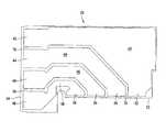
- FIG. 1illustrates a right angle power connector 10 that includes a housing 12 and a number of electrical wafers 20 .
- the housing 12includes a cover portion 14 and a base portion 16 .
- the base portion 16includes a plurality of contacts 18 that form a daughter card interface 22 .
- the contacts 18have a resilient upper end 19 that receive an edge of wafer 20 .
- the mating face 24 of the connector 10defines a backplane connector interface.
- the connector 10is referred to as a daughter card assembly that may be used to interconnect a daughter board to a backplane circuit.
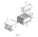
- FIG. 2shows an exploded view of the connector 10 of FIG. 1 .
- the housing base 16includes a plurality of slots 28 .
- the wafers 20are received into slots 28 with a card edge connection.
- An alignment slot 30is formed into the back wall 31 of the housing base 16 at each slot 28 .
- the connector 10is modular in construction and includes a plurality of wafers 20 .
- sixteen wafers 20are included in the power connector 10 , however, fewer or more than sixteen of wafers 20 may be used.
- Each wafer 20includes a daughter card edge 32 and a backplane edge 34 .
- the daughter card edge 32includes a series of contact pads 52 , 54 , 56 , and 58 .
- the backplane edge 34includes backplane contact pads 42 , 44 , 46 , and 48 . For purposes of illustration, only four contact pads are shown along edges 32 and 34 of the wafer 20 . It is to be understood, however, that any number of contact pads may be present.
- Each wafer 20is received in a slot 28 in the housing base 16 .
- the wafers 20are inserted into slots 28 in a downward direction indicated by the arrow A.
- the resilient ends 19 of contacts 18engage the daughter card contact pads 52 , 54 , 56 , and 58 on the wafer 20 to connect each wafer to the daughter card interface 22 .
- the contacts 18extend through the housing base 16 to become part of the daughter card interface 22 .
- the housing cover 14includes a plurality of alignment apertures 26 that receive the backplane edges 34 of wafers 20 .
- the apertures 26hold and stabilize the wafers 20 in slots 28 of the housing base 16 .
- the housing cover 14is attached by sliding the cover onto the base 16 in the direction of arrow B so that the backplane edges 34 of the wafers 20 extend through the apertures 26 .
- FIG. 3illustrates wafer 20 in detail.
- wafer 20is a printed circuit board (PCB) wafer.
- PCBprinted circuit board
- Each wafer 20includes a number of contact pads along the daughter card edge 32 and a comparable number of contact pads along the backplane edge 34 .
- four contact pads 52 , 54 , 56 , and 58are positioned along the daughter card edge 32 and four contact pads 42 , 44 , 46 , and 48 are positioned along the backplane edge 34 .
- Conductive paths or electrical traces 62 , 64 , 66 , and 68interconnect pairs of daughter card and backplane contact pads. Trace 62 connects daughter card contact pad 52 with backplane contact pad 42 .
- each wafer 20can have greater than or fewer than four traces.
- the wafer 20is illustrated as L-shaped, however other geometries are also possible.
- Daughter card edge 32 and backplane edge 34are substantially perpendicular to each other. However, in alternative embodiments, it is contemplated that edges 32 and 34 may intersect at other than a right angle. Due to the angular relationship, the current flow paths between corresponding daughter card and backplane contact pads, 42 and 52 , 44 and 54 , 46 and 56 , and 48 and 58 vary in length. To adjust for these flow path length differences, traces 62 , 64 , 66 , and 68 are configured so that the resistance of each trace between the daughter card and corresponding backplane contact pads 42 and 52 , 44 and 54 , 46 and 56 , and 48 and 58 is substantially equal so that current flow is evenly distributed through the wafer 20 .
- the even distribution of current flow through the wafer 20facilitates the avoidance of hot spots, particularly at the contacts of the backplane interface connector, as will be described, that often results from excessive current flow along flow paths of comparatively lower resistance. With an even distribution of current and a resulting even distribution of heating, more throughput through the connector 10 is possible.
- the resistance of the flow paths between the daughter card and backplane contact pads 42 and 52 , 44 and 54 , 46 and 56 , and 48 and 58can be changed by adjusting the geometric shape of the interconnecting traces 62 through 68 .
- Rresistance
- pa material conductivity constant
- Lpath length
- Across-sectional area
- the path length between the contact pads 52 and 42is established so that the trace area is adjusted for making final resistance balancing adjustments.
- the results of this analysisis reflected in FIG. 3 where the longest trace 62 , between daughter card contact pad 52 and backplane contact pad 42 , has the longest flow path and also the largest area, while the shortest trace 68 , has the shortest length and smallest area. That is, the length of each conductive path or trace 62 , 64 , 66 , and 68 is proportional to a minimum width of the respective trace.
- successive conductive paths along edges 32 and 34have increasing lengths and increasing widths, and thus, increasing areas.
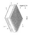
- FIG. 4illustrates an exemplary backplane interface mating connector 80 suitable for use with the connector 10 .
- the mating connector 80includes a housing 82 , a connector mating face 84 , and a backplane mating face 86 .
- a plurality of backplane contacts 88are received in contact cavities 92 in the housing 82 .
- Housing 82also includes a plurality of channels 90 that receive the backplane edges 34 of the wafers 20 when the mating connector 80 is mated with the connector 10 .
- Contacts 88have ends 94 that extend through the contact cavities 92 to engage the backplane contact pads 42 , 44 , 46 , and 48 on wafer 20 when connectors 10 and 80 are joined.
- the connector 10is attached to a daughter board through the daughter card interface 22 .
- the daughter boardtypically includes a multi-layered printed circuit board with multiple planes connected with through holes.
- the various planesinterface to a wafer 20 within the connector 10 via the resilient ends 19 of contacts 18 .
- the connector 10is modular and can be varied in size, e.g. the number of wafers 20 , to match the interconnection requirements of the particular application.
- the connector 10can include up to sixteen wafers 20 . Alternatively, being modular in form, any number of wafers 20 may be incorporated into the connector 10 .
- the backplane mating connector 80completes the connection between the daughter board and the backplane circuit through the terminal contacts 88 in the connector 80 .
- the backplanealso typically includes a multi-layered printed circuit board with through hole connections to the various layers. Using the connector 10 , power is delivered to the backplane interface 24 evenly distributed over the backplane contacts 42 , 44 , 46 , and 48 of each wafer 20 .
- the connector 10may also be used in signal applications. Further, the connector 10 may include both wafers adapted for signal transmission and wafers designed for power transmission in a common connector.
- the embodiments thus describedprovide a right angle power connector with resistively matched conductive paths through the right angle connector, so that current flow evenly distributed over the flow paths of the connector.
Landscapes
- Coupling Device And Connection With Printed Circuit (AREA)
- Details Of Connecting Devices For Male And Female Coupling (AREA)
Abstract
Description

Claims (20)
Priority Applications (1)
| Application Number | Priority Date | Filing Date | Title |
|---|---|---|---|
| US10/652,956US6811440B1 (en) | 2003-08-29 | 2003-08-29 | Power connector |
Applications Claiming Priority (1)
| Application Number | Priority Date | Filing Date | Title |
|---|---|---|---|
| US10/652,956US6811440B1 (en) | 2003-08-29 | 2003-08-29 | Power connector |
Publications (1)
| Publication Number | Publication Date |
|---|---|
| US6811440B1true US6811440B1 (en) | 2004-11-02 |
Family
ID=33300250
Family Applications (1)
| Application Number | Title | Priority Date | Filing Date |
|---|---|---|---|
| US10/652,956Expired - LifetimeUS6811440B1 (en) | 2003-08-29 | 2003-08-29 | Power connector |
Country Status (1)
| Country | Link |
|---|---|
| US (1) | US6811440B1 (en) |
Cited By (57)
| Publication number | Priority date | Publication date | Assignee | Title |
|---|---|---|---|---|
| US20050048817A1 (en)* | 2003-09-03 | 2005-03-03 | Cohen Thomas S. | High speed, high density electrical connector |
| US6932649B1 (en)* | 2004-03-19 | 2005-08-23 | Tyco Electronics Corporation | Active wafer for improved gigabit signal recovery, in a serial point-to-point architecture |
| US20060035521A1 (en)* | 2004-08-16 | 2006-02-16 | Ngo Hung V | Power contact having current flow guiding feature and electrical connector containing same |
| US20060046568A1 (en)* | 2004-08-31 | 2006-03-02 | Consoli John J | Electrical connector power wafers |
| US7402064B2 (en) | 2003-12-31 | 2008-07-22 | Fci Americas Technology, Inc. | Electrical power contacts and connectors comprising same |
| US20080214055A1 (en)* | 2006-12-20 | 2008-09-04 | Gulla Joseph M | Electrical connector assembly |
| US7425145B2 (en) | 2006-05-26 | 2008-09-16 | Fci Americas Technology, Inc. | Connectors and contacts for transmitting electrical power |
| US7458839B2 (en) | 2006-02-21 | 2008-12-02 | Fci Americas Technology, Inc. | Electrical connectors having power contacts with alignment and/or restraining features |
| US7476108B2 (en) | 2004-12-22 | 2009-01-13 | Fci Americas Technology, Inc. | Electrical power connectors with cooling features |
| US7541135B2 (en) | 2005-04-05 | 2009-06-02 | Fci Americas Technology, Inc. | Power contact having conductive plates with curved portions contact beams and board tails |
| USD606496S1 (en) | 2009-01-16 | 2009-12-22 | Fci Americas Technology, Inc. | Right-angle electrical connector |
| USD606497S1 (en) | 2009-01-16 | 2009-12-22 | Fci Americas Technology, Inc. | Vertical electrical connector |
| US7641500B2 (en) | 2007-04-04 | 2010-01-05 | Fci Americas Technology, Inc. | Power cable connector system |
| USD608293S1 (en) | 2009-01-16 | 2010-01-19 | Fci Americas Technology, Inc. | Vertical electrical connector |
| USD610548S1 (en) | 2009-01-16 | 2010-02-23 | Fci Americas Technology, Inc. | Right-angle electrical connector |
| US20100093209A1 (en)* | 2008-10-15 | 2010-04-15 | Hon Hai Precision Industry Co., Ltd. | Electrical connector assembly with improved resisting structure to ensure reliable contacting between ground shields thereof |
| USRE41283E1 (en) | 2003-01-28 | 2010-04-27 | Fci Americas Technology, Inc. | Power connector with safety feature |
| US7726982B2 (en) | 2006-06-15 | 2010-06-01 | Fci Americas Technology, Inc. | Electrical connectors with air-circulation features |
| CN101728667A (en)* | 2008-10-16 | 2010-06-09 | 富士康(昆山)电脑接插件有限公司 | Electric connector |
| USD618181S1 (en) | 2009-04-03 | 2010-06-22 | Fci Americas Technology, Inc. | Asymmetrical electrical connector |
| USD618180S1 (en) | 2009-04-03 | 2010-06-22 | Fci Americas Technology, Inc. | Asymmetrical electrical connector |
| US7749009B2 (en) | 2005-01-31 | 2010-07-06 | Fci Americas Technology, Inc. | Surface-mount connector |
| USD619099S1 (en) | 2009-01-30 | 2010-07-06 | Fci Americas Technology, Inc. | Electrical connector |
| US7762857B2 (en) | 2007-10-01 | 2010-07-27 | Fci Americas Technology, Inc. | Power connectors with contact-retention features |
| US20100210123A1 (en)* | 2009-02-16 | 2010-08-19 | Tyco Electronics Corporation | Card edge module connector assembly |
| US7905731B2 (en) | 2007-05-21 | 2011-03-15 | Fci Americas Technology, Inc. | Electrical connector with stress-distribution features |
| USD640637S1 (en) | 2009-01-16 | 2011-06-28 | Fci Americas Technology Llc | Vertical electrical connector |
| US20110165784A1 (en)* | 2008-01-17 | 2011-07-07 | Amphenol Corporation | Electrical connector assembly |
| US8062051B2 (en) | 2008-07-29 | 2011-11-22 | Fci Americas Technology Llc | Electrical communication system having latching and strain relief features |
| USD664096S1 (en) | 2009-01-16 | 2012-07-24 | Fci Americas Technology Llc | Vertical electrical connector |
| US8323049B2 (en) | 2009-01-30 | 2012-12-04 | Fci Americas Technology Llc | Electrical connector having power contacts |
| US20130277186A1 (en)* | 2012-04-23 | 2013-10-24 | Fujitsu Component Limited | Touch panel |
| USD718253S1 (en) | 2012-04-13 | 2014-11-25 | Fci Americas Technology Llc | Electrical cable connector |
| US8905651B2 (en) | 2012-01-31 | 2014-12-09 | Fci | Dismountable optical coupling device |
| USD720698S1 (en) | 2013-03-15 | 2015-01-06 | Fci Americas Technology Llc | Electrical cable connector |
| US8944831B2 (en) | 2012-04-13 | 2015-02-03 | Fci Americas Technology Llc | Electrical connector having ribbed ground plate with engagement members |
| USD727268S1 (en) | 2012-04-13 | 2015-04-21 | Fci Americas Technology Llc | Vertical electrical connector |
| USD727852S1 (en) | 2012-04-13 | 2015-04-28 | Fci Americas Technology Llc | Ground shield for a right angle electrical connector |
| US9017114B2 (en) | 2009-09-09 | 2015-04-28 | Amphenol Corporation | Mating contacts for high speed electrical connectors |
| US9048583B2 (en) | 2009-03-19 | 2015-06-02 | Fci Americas Technology Llc | Electrical connector having ribbed ground plate |
| USD733662S1 (en) | 2013-01-25 | 2015-07-07 | Fci Americas Technology Llc | Connector housing for electrical connector |
| US20150207247A1 (en)* | 2011-08-08 | 2015-07-23 | Molex Incorporated | Connector with tuned channel |
| WO2015186960A1 (en)* | 2014-06-03 | 2015-12-10 | Manycoresoft Co., Ltd. | Power connector device |
| USD746236S1 (en) | 2012-07-11 | 2015-12-29 | Fci Americas Technology Llc | Electrical connector housing |
| US9257778B2 (en) | 2012-04-13 | 2016-02-09 | Fci Americas Technology | High speed electrical connector |
| US9543703B2 (en) | 2012-07-11 | 2017-01-10 | Fci Americas Technology Llc | Electrical connector with reduced stack height |
| US9583851B2 (en)* | 2015-06-11 | 2017-02-28 | Lenovo Enterprise Solutions (Singapore) Pte. Ltd. | Orthogonal card edge connector |
| US9997868B1 (en) | 2017-07-24 | 2018-06-12 | Te Connectivity Corporation | Electrical connector with improved impedance characteristics |
| US10128597B2 (en) | 2016-06-10 | 2018-11-13 | Te Connectivity Corporation | Electrical contact pad for electrically contacting a connector |
| US10263352B2 (en) | 2016-06-10 | 2019-04-16 | Te Connectivity Corporation | Electrical contact pad for electrically contacting a connector |
| US10320099B2 (en) | 2016-06-10 | 2019-06-11 | Te Connectivity Corporation | Connector with asymmetric base section |
| US10965062B1 (en) | 2020-03-26 | 2021-03-30 | TE Connectivity Services Gmbh | Modular electrical connector with conductive coating to reduce crosstalk |
| US10998678B1 (en) | 2020-03-26 | 2021-05-04 | TE Connectivity Services Gmbh | Modular electrical connector with additional grounding |
| US11025014B1 (en) | 2020-03-26 | 2021-06-01 | TE CONNECTNITY SERVICES GmbH | Shield component for use with modular electrical connector to reduce crosstalk |
| US11031734B1 (en) | 2020-03-26 | 2021-06-08 | TE Connectivity Services Gmbh | Modular electrical connector with reduced crosstalk |
| US11264749B2 (en) | 2020-03-26 | 2022-03-01 | TE Connectivity Services Gmbh | Modular connector with printed circuit board wafer to reduce crosstalk |
| US11297712B2 (en) | 2020-03-26 | 2022-04-05 | TE Connectivity Services Gmbh | Modular printed circuit board wafer connector with reduced crosstalk |
Citations (6)
| Publication number | Priority date | Publication date | Assignee | Title |
|---|---|---|---|---|
| US4861272A (en) | 1988-03-31 | 1989-08-29 | E. I. Du Pont De Nemours And Company | Impedance controlled connector interface |
| US5066236A (en) | 1989-10-10 | 1991-11-19 | Amp Incorporated | Impedance matched backplane connector |
| US6293827B1 (en)* | 2000-02-03 | 2001-09-25 | Teradyne, Inc. | Differential signal electrical connector |
| US6379188B1 (en) | 1997-02-07 | 2002-04-30 | Teradyne, Inc. | Differential signal electrical connectors |
| US20030228776A1 (en)* | 2002-06-06 | 2003-12-11 | International Business Machines Corporation | Right angle board-to-board connector with balanced impedance |
| US6705902B1 (en)* | 2002-12-03 | 2004-03-16 | Hon Hai Precision Ind. Co., Ltd. | Connector assembly having contacts with uniform electrical property of resistance |
- 2003
- 2003-08-29USUS10/652,956patent/US6811440B1/ennot_activeExpired - Lifetime
Patent Citations (6)
| Publication number | Priority date | Publication date | Assignee | Title |
|---|---|---|---|---|
| US4861272A (en) | 1988-03-31 | 1989-08-29 | E. I. Du Pont De Nemours And Company | Impedance controlled connector interface |
| US5066236A (en) | 1989-10-10 | 1991-11-19 | Amp Incorporated | Impedance matched backplane connector |
| US6379188B1 (en) | 1997-02-07 | 2002-04-30 | Teradyne, Inc. | Differential signal electrical connectors |
| US6293827B1 (en)* | 2000-02-03 | 2001-09-25 | Teradyne, Inc. | Differential signal electrical connector |
| US20030228776A1 (en)* | 2002-06-06 | 2003-12-11 | International Business Machines Corporation | Right angle board-to-board connector with balanced impedance |
| US6705902B1 (en)* | 2002-12-03 | 2004-03-16 | Hon Hai Precision Ind. Co., Ltd. | Connector assembly having contacts with uniform electrical property of resistance |
Cited By (103)
| Publication number | Priority date | Publication date | Assignee | Title |
|---|---|---|---|---|
| USRE41283E1 (en) | 2003-01-28 | 2010-04-27 | Fci Americas Technology, Inc. | Power connector with safety feature |
| US7074086B2 (en)* | 2003-09-03 | 2006-07-11 | Amphenol Corporation | High speed, high density electrical connector |
| US20050048817A1 (en)* | 2003-09-03 | 2005-03-03 | Cohen Thomas S. | High speed, high density electrical connector |
| US7402064B2 (en) | 2003-12-31 | 2008-07-22 | Fci Americas Technology, Inc. | Electrical power contacts and connectors comprising same |
| US8062046B2 (en) | 2003-12-31 | 2011-11-22 | Fci Americas Technology Llc | Electrical power contacts and connectors comprising same |
| US7690937B2 (en) | 2003-12-31 | 2010-04-06 | Fci Americas Technology, Inc. | Electrical power contacts and connectors comprising same |
| US8187017B2 (en) | 2003-12-31 | 2012-05-29 | Fci Americas Technology Llc | Electrical power contacts and connectors comprising same |
| US7862359B2 (en) | 2003-12-31 | 2011-01-04 | Fci Americas Technology Llc | Electrical power contacts and connectors comprising same |
| US7775822B2 (en) | 2003-12-31 | 2010-08-17 | Fci Americas Technology, Inc. | Electrical connectors having power contacts with alignment/or restraining features |
| US7452249B2 (en) | 2003-12-31 | 2008-11-18 | Fci Americas Technology, Inc. | Electrical power contacts and connectors comprising same |
| US6932649B1 (en)* | 2004-03-19 | 2005-08-23 | Tyco Electronics Corporation | Active wafer for improved gigabit signal recovery, in a serial point-to-point architecture |
| US7182642B2 (en) | 2004-08-16 | 2007-02-27 | Fci Americas Technology, Inc. | Power contact having current flow guiding feature and electrical connector containing same |
| US20060035521A1 (en)* | 2004-08-16 | 2006-02-16 | Ngo Hung V | Power contact having current flow guiding feature and electrical connector containing same |
| US20060046568A1 (en)* | 2004-08-31 | 2006-03-02 | Consoli John J | Electrical connector power wafers |
| US7175445B2 (en) | 2004-08-31 | 2007-02-13 | Tyco Electronics Corporation | Electrical connector power wafers |
| US7476108B2 (en) | 2004-12-22 | 2009-01-13 | Fci Americas Technology, Inc. | Electrical power connectors with cooling features |
| US7749009B2 (en) | 2005-01-31 | 2010-07-06 | Fci Americas Technology, Inc. | Surface-mount connector |
| US7541135B2 (en) | 2005-04-05 | 2009-06-02 | Fci Americas Technology, Inc. | Power contact having conductive plates with curved portions contact beams and board tails |
| US7458839B2 (en) | 2006-02-21 | 2008-12-02 | Fci Americas Technology, Inc. | Electrical connectors having power contacts with alignment and/or restraining features |
| US7425145B2 (en) | 2006-05-26 | 2008-09-16 | Fci Americas Technology, Inc. | Connectors and contacts for transmitting electrical power |
| US7726982B2 (en) | 2006-06-15 | 2010-06-01 | Fci Americas Technology, Inc. | Electrical connectors with air-circulation features |
| US7985097B2 (en) | 2006-12-20 | 2011-07-26 | Amphenol Corporation | Electrical connector assembly |
| US20080214055A1 (en)* | 2006-12-20 | 2008-09-04 | Gulla Joseph M | Electrical connector assembly |
| US7641500B2 (en) | 2007-04-04 | 2010-01-05 | Fci Americas Technology, Inc. | Power cable connector system |
| US7905731B2 (en) | 2007-05-21 | 2011-03-15 | Fci Americas Technology, Inc. | Electrical connector with stress-distribution features |
| US7762857B2 (en) | 2007-10-01 | 2010-07-27 | Fci Americas Technology, Inc. | Power connectors with contact-retention features |
| US8469720B2 (en) | 2008-01-17 | 2013-06-25 | Amphenol Corporation | Electrical connector assembly |
| US9564696B2 (en) | 2008-01-17 | 2017-02-07 | Amphenol Corporation | Electrical connector assembly |
| US8727791B2 (en) | 2008-01-17 | 2014-05-20 | Amphenol Corporation | Electrical connector assembly |
| US9190745B2 (en) | 2008-01-17 | 2015-11-17 | Amphenol Corporation | Electrical connector assembly |
| US20110165784A1 (en)* | 2008-01-17 | 2011-07-07 | Amphenol Corporation | Electrical connector assembly |
| US8062051B2 (en) | 2008-07-29 | 2011-11-22 | Fci Americas Technology Llc | Electrical communication system having latching and strain relief features |
| US20100093209A1 (en)* | 2008-10-15 | 2010-04-15 | Hon Hai Precision Industry Co., Ltd. | Electrical connector assembly with improved resisting structure to ensure reliable contacting between ground shields thereof |
| CN101728667B (en)* | 2008-10-16 | 2013-08-14 | 富士康(昆山)电脑接插件有限公司 | Electric connector |
| CN101728667A (en)* | 2008-10-16 | 2010-06-09 | 富士康(昆山)电脑接插件有限公司 | Electric connector |
| USD606496S1 (en) | 2009-01-16 | 2009-12-22 | Fci Americas Technology, Inc. | Right-angle electrical connector |
| USD641709S1 (en) | 2009-01-16 | 2011-07-19 | Fci Americas Technology Llc | Vertical electrical connector |
| USD606497S1 (en) | 2009-01-16 | 2009-12-22 | Fci Americas Technology, Inc. | Vertical electrical connector |
| USD647058S1 (en) | 2009-01-16 | 2011-10-18 | Fci Americas Technology Llc | Vertical electrical connector |
| USD696199S1 (en) | 2009-01-16 | 2013-12-24 | Fci Americas Technology Llc | Vertical electrical connector |
| USD651981S1 (en) | 2009-01-16 | 2012-01-10 | Fci Americas Technology Llc | Vertical electrical connector |
| USD608293S1 (en) | 2009-01-16 | 2010-01-19 | Fci Americas Technology, Inc. | Vertical electrical connector |
| USD660245S1 (en) | 2009-01-16 | 2012-05-22 | Fci Americas Technology Llc | Vertical electrical connector |
| USD640637S1 (en) | 2009-01-16 | 2011-06-28 | Fci Americas Technology Llc | Vertical electrical connector |
| USD664096S1 (en) | 2009-01-16 | 2012-07-24 | Fci Americas Technology Llc | Vertical electrical connector |
| USD610548S1 (en) | 2009-01-16 | 2010-02-23 | Fci Americas Technology, Inc. | Right-angle electrical connector |
| USD619099S1 (en) | 2009-01-30 | 2010-07-06 | Fci Americas Technology, Inc. | Electrical connector |
| US8323049B2 (en) | 2009-01-30 | 2012-12-04 | Fci Americas Technology Llc | Electrical connector having power contacts |
| US7993147B2 (en)* | 2009-02-16 | 2011-08-09 | Tyco Electronics Corporation | Card edge module connector assembly |
| US20100210123A1 (en)* | 2009-02-16 | 2010-08-19 | Tyco Electronics Corporation | Card edge module connector assembly |
| US10096921B2 (en) | 2009-03-19 | 2018-10-09 | Fci Usa Llc | Electrical connector having ribbed ground plate |
| US9048583B2 (en) | 2009-03-19 | 2015-06-02 | Fci Americas Technology Llc | Electrical connector having ribbed ground plate |
| US9461410B2 (en) | 2009-03-19 | 2016-10-04 | Fci Americas Technology Llc | Electrical connector having ribbed ground plate |
| US10720721B2 (en) | 2009-03-19 | 2020-07-21 | Fci Usa Llc | Electrical connector having ribbed ground plate |
| USD618181S1 (en) | 2009-04-03 | 2010-06-22 | Fci Americas Technology, Inc. | Asymmetrical electrical connector |
| USD618180S1 (en) | 2009-04-03 | 2010-06-22 | Fci Americas Technology, Inc. | Asymmetrical electrical connector |
| USD653621S1 (en) | 2009-04-03 | 2012-02-07 | Fci Americas Technology Llc | Asymmetrical electrical connector |
| US9780493B2 (en) | 2009-09-09 | 2017-10-03 | Amphenol Corporation | Mating contacts for high speed electrical connectors |
| US9017114B2 (en) | 2009-09-09 | 2015-04-28 | Amphenol Corporation | Mating contacts for high speed electrical connectors |
| US20150207247A1 (en)* | 2011-08-08 | 2015-07-23 | Molex Incorporated | Connector with tuned channel |
| US20170302036A1 (en)* | 2011-08-08 | 2017-10-19 | Molex, Llc | Connector with tuned channel |
| US9312618B2 (en)* | 2011-08-08 | 2016-04-12 | Molex, Llc | Connector with tuned channel |
| US20200106218A1 (en)* | 2011-08-08 | 2020-04-02 | Molex, Llc | Connector with tuned channel |
| US9711911B2 (en)* | 2011-08-08 | 2017-07-18 | Molex, Llc | Connector with tuned channel |
| US10439334B2 (en)* | 2011-08-08 | 2019-10-08 | Molex, Llc | Connector with tuned channel |
| US10950982B2 (en)* | 2011-08-08 | 2021-03-16 | Molex, Llc | Connector with tuned channel |
| US20160190747A1 (en)* | 2011-08-08 | 2016-06-30 | Molex, Llc | Connector with tuned channel |
| US8905651B2 (en) | 2012-01-31 | 2014-12-09 | Fci | Dismountable optical coupling device |
| US8944831B2 (en) | 2012-04-13 | 2015-02-03 | Fci Americas Technology Llc | Electrical connector having ribbed ground plate with engagement members |
| US9831605B2 (en) | 2012-04-13 | 2017-11-28 | Fci Americas Technology Llc | High speed electrical connector |
| USD727268S1 (en) | 2012-04-13 | 2015-04-21 | Fci Americas Technology Llc | Vertical electrical connector |
| USD750025S1 (en) | 2012-04-13 | 2016-02-23 | Fci Americas Technology Llc | Vertical electrical connector |
| US9257778B2 (en) | 2012-04-13 | 2016-02-09 | Fci Americas Technology | High speed electrical connector |
| USD727852S1 (en) | 2012-04-13 | 2015-04-28 | Fci Americas Technology Llc | Ground shield for a right angle electrical connector |
| USD718253S1 (en) | 2012-04-13 | 2014-11-25 | Fci Americas Technology Llc | Electrical cable connector |
| USD816044S1 (en) | 2012-04-13 | 2018-04-24 | Fci Americas Technology Llc | Electrical cable connector |
| USD750030S1 (en) | 2012-04-13 | 2016-02-23 | Fci Americas Technology Llc | Electrical cable connector |
| USD790471S1 (en) | 2012-04-13 | 2017-06-27 | Fci Americas Technology Llc | Vertical electrical connector |
| USD748063S1 (en) | 2012-04-13 | 2016-01-26 | Fci Americas Technology Llc | Electrical ground shield |
| US20130277186A1 (en)* | 2012-04-23 | 2013-10-24 | Fujitsu Component Limited | Touch panel |
| USD746236S1 (en) | 2012-07-11 | 2015-12-29 | Fci Americas Technology Llc | Electrical connector housing |
| US9543703B2 (en) | 2012-07-11 | 2017-01-10 | Fci Americas Technology Llc | Electrical connector with reduced stack height |
| US9871323B2 (en) | 2012-07-11 | 2018-01-16 | Fci Americas Technology Llc | Electrical connector with reduced stack height |
| USD751507S1 (en) | 2012-07-11 | 2016-03-15 | Fci Americas Technology Llc | Electrical connector |
| USD745852S1 (en) | 2013-01-25 | 2015-12-22 | Fci Americas Technology Llc | Electrical connector |
| USD733662S1 (en) | 2013-01-25 | 2015-07-07 | Fci Americas Technology Llc | Connector housing for electrical connector |
| USD772168S1 (en) | 2013-01-25 | 2016-11-22 | Fci Americas Technology Llc | Connector housing for electrical connector |
| USD766832S1 (en) | 2013-01-25 | 2016-09-20 | Fci Americas Technology Llc | Electrical connector |
| USD720698S1 (en) | 2013-03-15 | 2015-01-06 | Fci Americas Technology Llc | Electrical cable connector |
| WO2015186960A1 (en)* | 2014-06-03 | 2015-12-10 | Manycoresoft Co., Ltd. | Power connector device |
| US20170133780A1 (en)* | 2015-06-11 | 2017-05-11 | Lenovo Enterprise Solutions (Singapore) Pte. Ltd. | Orthogonal card edge connector |
| US9583851B2 (en)* | 2015-06-11 | 2017-02-28 | Lenovo Enterprise Solutions (Singapore) Pte. Ltd. | Orthogonal card edge connector |
| US10320099B2 (en) | 2016-06-10 | 2019-06-11 | Te Connectivity Corporation | Connector with asymmetric base section |
| US10263352B2 (en) | 2016-06-10 | 2019-04-16 | Te Connectivity Corporation | Electrical contact pad for electrically contacting a connector |
| US10128597B2 (en) | 2016-06-10 | 2018-11-13 | Te Connectivity Corporation | Electrical contact pad for electrically contacting a connector |
| EP3469862B1 (en)* | 2016-06-10 | 2024-10-09 | TE Connectivity Solutions GmbH | Electrical contact pad for electrically contacting a connector |
| US9997868B1 (en) | 2017-07-24 | 2018-06-12 | Te Connectivity Corporation | Electrical connector with improved impedance characteristics |
| US10965062B1 (en) | 2020-03-26 | 2021-03-30 | TE Connectivity Services Gmbh | Modular electrical connector with conductive coating to reduce crosstalk |
| US10998678B1 (en) | 2020-03-26 | 2021-05-04 | TE Connectivity Services Gmbh | Modular electrical connector with additional grounding |
| US11025014B1 (en) | 2020-03-26 | 2021-06-01 | TE CONNECTNITY SERVICES GmbH | Shield component for use with modular electrical connector to reduce crosstalk |
| US11031734B1 (en) | 2020-03-26 | 2021-06-08 | TE Connectivity Services Gmbh | Modular electrical connector with reduced crosstalk |
| US11264749B2 (en) | 2020-03-26 | 2022-03-01 | TE Connectivity Services Gmbh | Modular connector with printed circuit board wafer to reduce crosstalk |
| US11297712B2 (en) | 2020-03-26 | 2022-04-05 | TE Connectivity Services Gmbh | Modular printed circuit board wafer connector with reduced crosstalk |
Similar Documents
| Publication | Publication Date | Title |
|---|---|---|
| US6811440B1 (en) | Power connector | |
| US11444398B2 (en) | High density electrical connector | |
| US10361520B2 (en) | High density electrical connector with shield plate louvers | |
| CN212342862U (en) | Electric connector, printed circuit board and conductive member | |
| US7591683B2 (en) | Contact terminal, extender with improved ground contact, and method for making the extender | |
| US7021942B2 (en) | Area array connector having stacked contacts for improved current carrying capacity | |
| JP4525959B2 (en) | Electrical connector having a housing for holding parallel circuit boards | |
| EP1382094B1 (en) | Electrical connector assembly for orthogonally mating circuit boards | |
| US7182642B2 (en) | Power contact having current flow guiding feature and electrical connector containing same | |
| US7497739B2 (en) | Electrical connector assembly | |
| US7985079B1 (en) | Connector assembly having a mating adapter | |
| US7425137B1 (en) | Connector for stacking circuit boards | |
| US7713083B1 (en) | Jumper device for controlling connection of pins of electrical device on mainboard | |
| US7220130B2 (en) | Electrical connector and system having contact array interface for engaging contacts at varying centerline spacing | |
| CN116683209A (en) | Hybrid card edge connector and power terminals for high power applications | |
| TW201707284A (en) | Wafer for electrical connector | |
| US10958002B2 (en) | Electrical power connector configured for high current density | |
| EP0107288A1 (en) | Electrical connector assembly for terminating flat shielded electrical cable | |
| KR101878049B1 (en) | Connector | |
| US7544104B2 (en) | Electrical interconnection with terminals in columns | |
| US7195493B1 (en) | Land grid array socket connector with location members | |
| US7175445B2 (en) | Electrical connector power wafers | |
| US5588849A (en) | Connector with pin terminals adapted for surface mounting | |
| US8083550B2 (en) | Electrical connector with cover | |
| US6369336B1 (en) | Printed circuit board |
Legal Events
| Date | Code | Title | Description |
|---|---|---|---|
| AS | Assignment | Owner name:TYCO ELECTRONICS CORPRATION, PENNSYLVANIA Free format text:ASSIGNMENT OF ASSIGNORS INTEREST;ASSIGNORS:ROTHERMEL, BRENT RYAN;SHARF, ALEX MICHAEL;GLOVER, DOUGLAS W.;REEL/FRAME:014456/0283;SIGNING DATES FROM 20030728 TO 20030729 | |
| STCF | Information on status: patent grant | Free format text:PATENTED CASE | |
| FPAY | Fee payment | Year of fee payment:4 | |
| REMI | Maintenance fee reminder mailed | ||
| FPAY | Fee payment | Year of fee payment:8 | |
| FPAY | Fee payment | Year of fee payment:12 | |
| AS | Assignment | Owner name:TE CONNECTIVITY CORPORATION, PENNSYLVANIA Free format text:CHANGE OF NAME;ASSIGNOR:TYCO ELECTRONICS CORPORATION;REEL/FRAME:041350/0085 Effective date:20170101 | |
| AS | Assignment | Owner name:TE CONNECTIVITY SERVICES GMBH, SWITZERLAND Free format text:CHANGE OF ADDRESS;ASSIGNOR:TE CONNECTIVITY SERVICES GMBH;REEL/FRAME:056514/0015 Effective date:20191101 Owner name:TE CONNECTIVITY SERVICES GMBH, SWITZERLAND Free format text:ASSIGNMENT OF ASSIGNORS INTEREST;ASSIGNOR:TE CONNECTIVITY CORPORATION;REEL/FRAME:056514/0048 Effective date:20180928 | |
| AS | Assignment | Owner name:TE CONNECTIVITY SOLUTIONS GMBH, SWITZERLAND Free format text:MERGER;ASSIGNOR:TE CONNECTIVITY SERVICES GMBH;REEL/FRAME:060885/0482 Effective date:20220301 |