US6810454B2 - Information processing apparatus having a bus using the protocol of the acknowledge type in the source clock synchronous system - Google Patents
Information processing apparatus having a bus using the protocol of the acknowledge type in the source clock synchronous systemDownload PDFInfo
- Publication number
- US6810454B2 US6810454B2US10/337,729US33772903AUS6810454B2US 6810454 B2US6810454 B2US 6810454B2US 33772903 AUS33772903 AUS 33772903AUS 6810454 B2US6810454 B2US 6810454B2
- Authority
- US
- United States
- Prior art keywords
- bus
- transfer
- source clock
- information processing
- module
- Prior art date
- Legal status (The legal status is an assumption and is not a legal conclusion. Google has not performed a legal analysis and makes no representation as to the accuracy of the status listed.)
- Expired - Fee Related
Links
Images


Classifications
- G—PHYSICS
- G06—COMPUTING OR CALCULATING; COUNTING
- G06F—ELECTRIC DIGITAL DATA PROCESSING
- G06F13/00—Interconnection of, or transfer of information or other signals between, memories, input/output devices or central processing units
- G06F13/38—Information transfer, e.g. on bus
- G06F13/40—Bus structure
- G06F13/4004—Coupling between buses
- G06F13/4027—Coupling between buses using bus bridges
- G06F13/405—Coupling between buses using bus bridges where the bridge performs a synchronising function
- G06F13/4059—Coupling between buses using bus bridges where the bridge performs a synchronising function where the synchronisation uses buffers, e.g. for speed matching between buses
- Y—GENERAL TAGGING OF NEW TECHNOLOGICAL DEVELOPMENTS; GENERAL TAGGING OF CROSS-SECTIONAL TECHNOLOGIES SPANNING OVER SEVERAL SECTIONS OF THE IPC; TECHNICAL SUBJECTS COVERED BY FORMER USPC CROSS-REFERENCE ART COLLECTIONS [XRACs] AND DIGESTS
- Y02—TECHNOLOGIES OR APPLICATIONS FOR MITIGATION OR ADAPTATION AGAINST CLIMATE CHANGE
- Y02D—CLIMATE CHANGE MITIGATION TECHNOLOGIES IN INFORMATION AND COMMUNICATION TECHNOLOGIES [ICT], I.E. INFORMATION AND COMMUNICATION TECHNOLOGIES AIMING AT THE REDUCTION OF THEIR OWN ENERGY USE
- Y02D10/00—Energy efficient computing, e.g. low power processors, power management or thermal management
Definitions
- the present inventionrelates to an information processing apparatus such as personal computers and work stations, and in particular to protocols of buses of these information processing apparatuses and internal buses of LSIs used in the information processing apparatus.
- Numeral 1301denotes a master module serving as a transfer source of data.
- Numeral 1303denotes a slave module serving as a transfer destination of data, and
- numeral 1304denotes a data bus.
- numerals 1400 and 1401denote timing relations between a system clock and output data observed on an output pin of the master module 1301 serving as the transfer source of data.
- numerals 1402 and 1403denote timing relations between the system clock and input data observed on an input pin of the slave module 1303 serving as the transfer destination of data.
- the clocks 1400 and 1402are distributed from the clock generator 1300 of FIG. 13 with the same phase.
- Data on the input pin of the slave module 1303is delayed from that on the output pin of the master module 1301 by a propagation delay time on the data bus 1304 . Since data must be transferred from the master module to the slave module in one cycle, the maximum operation frequency is typically determined on a synchronous bus by a maximum propagation delay time of the bus.
- a bus of a “source clock synchronous system”(or a source clock synchronous bus) is conceivable.
- a module serving as a transfer sourcetransmits a latch clock to be used in a module of a transfer destination together with transfer data.
- a bus configuration and a timing chart of a typical source clock synchronous systemare shown in FIGS. 15 and 16, respectively.
- numeral 1500denotes a signal line for a source clock which is transmitted from a master module serving as a transfer source to a slave module serving as a transfer destination.
- numerals 1600 and 1601denote timing relations between a source clock and output data observed on an output pin of the master module serving as the transfer source of data.
- Numerals 1602 and 1603denote timing relations between the source clock and input data observed on an input pin of the slave module serving as the transfer destination of data.
- FIG. 17shows transfer timing of the synchronous bus with a protocol of the acknowledge type.
- numeral 1700denotes a system clock common to modules on the bus
- numeral 1701denotes transfer data timing
- numeral 1702denotes acknowledge signal timing. If it is determined in the synchronous bus that a signal of the acknowledge type is issued necessarily two cycles after the data transfer cycle, association of transfer data with the report of the acknowledge type is very easy.
- the protocol of the acknowledge typethere are, for example, an acknowledge for notifying the master side that the slave side has certainly received data, a retry request for requesting the master side to retransfer data later because the slave side is not ready to receive data, and an error report for notifying the master side that data received by the slave side contained an error (such as a parity error).
- an error reportfor notifying the master side that data received by the slave side contained an error (such as a parity error).
- An object of the present inventionis to provide a bus of source clock synchronous system with a protocol of an acknowledge type in order to operate the bus with high reliability and a high efficiency and provide an information processing apparatus having a bus using the protocol of the acknowledge type in the source clock synchronous system.
- a source clock signaldedicated to acknowledge type signals on a signal line of a bus in order to transfer the acknowledge type signals as well by using the source clock synchronous system. Furthermore, in order to make possible control even if there are mixedly modules having different operation frequencies, an acknowledge signal is not provided for each cycle, but is provided for each basic transfer block having a substantial number of cycles.
- acknowledge type signalsare also transferred in the source clock synchronous system by using a source clock signal dedicated to the acknowledge type signals, a failure, on the master side, of acquisition of an acknowledge type signal from the slave side is prevented. Furthermore, since an acknowledge signal is provided for each basic transfer block having a substantial number of cycles, control becomes possible even if there are mixedly modules having different operation frequencies.
- a master moduleserving as a transfer source
- a slave moduleserving as a transfer destination
- a bus of a source clock synchronous systemand a means for transferring a signal based upon a protocol of an acknowledge type from the slave module to the master module via the bus of the source clock synchronous system.
- a source clock signal linededicated to the acknowledge type signals.
- the master modulea processor or an I/O (input/output) device is conceivable.
- an I/O device or a storageis conceivable.
- acknowledge reportindicating that the transfer from the master module to the slave module has been conducted
- a retry requestfor requesting reexecution because the slave module is not ready to receive data transferred from the master module
- error reportfor notifying the master module that transfer from the master module to the slave module has not been conducted correctly.
- acknowledge report and the retry requestare sent once for a plurality of transfer cycles.
- a method for transferring a signal of an acknowledge typeincludes the steps of transferring data and a source clock used as a latch clock from a master module to a slave module serving as a transfer destination via a bus of a source clock synchronous system, and transferring a signal based upon a protocol of the acknowledge type together with a source clock of the slave module from the slave module to the master module via the bus when the slave module has received the data and the latch clock transferred from the master module.
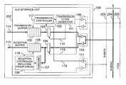
- FIG. 1is a block diagram showing an internal structure of a bus interface unit included in each of modules connected to a bus of the present invention
- FIG. 2is a block diagram showing connection relations using signal lines of the bus of the present invention.
- FIG. 3Ais a list of meaning of acknowledge type signal lines in the bus of the present invention.
- FIG. 3Bis an output timing diagram of acknowledge type signals
- FIG. 4is a command list of a multiplexed command/address/data bus of the bus of the present invention at the time of command output;
- FIG. 5is a timing chart of the present bus at the time of reading
- FIG. 6is a timing chart of the present bus at the time of writing
- FIG. 7is a timing chart in the case where other transfer has been inserted in a data phase of read transfer
- FIG. 8is a timing chart in the case where retry is requested from a slave module side at the time of write transfer of the present bus
- FIG. 9is a timing chart showing details of arbitration in the case where a bus right is moved during transfer of the present bus
- FIG. 10is a timing chart showing transfer using three different bus masters of the present bus.
- FIG. 11is a configuration diagram of an example of an information processing system using a bus of the present invention.
- FIG. 12is a configuration diagram of an example of an information processing system using a bus of the present invention.
- FIG. 13is a configuration diagram showing a basic transfer system of a conventional common clock synchronous bus
- FIG. 14is a timing chart showing a basic transfer system of a conventional common clock synchronous bus
- FIG. 15is a configuration diagram showing a basic transfer system of a source clock synchronous bus
- FIG. 16is a timing chart showing a basic transfer system of a source clock synchronous bus
- FIG. 17is a timing chart showing a basic transfer system of a common clock synchronous bus with acknowledge.
- FIG. 18is a block diagram showing a system configuration example in the case where a bus of the present invention has been applied to an internal bus of an LSI.
- FIGS. 1 through 18An embodiment of the present invention will now be described by referring to FIGS. 1 through 18.
- numeral 100denotes a module connected to a system bus of the present invention.
- Numeral 101denotes a transmission clock generator for generating a transmission clock to be transmitted to a slave together with data.
- Numeral 102denotes a transmission controller for controlling transmission timing and a transmission buffer.
- Numeral 103denotes a final stage buffer for data transmission.
- Numeral 104denotes an initial stage buffer for data reception.
- Numeral 105denotes a transmission data buffer (including command/address/data).
- Numeral 106denotes a reception data buffer (including command/address/data).
- Numeral 107denotes a command/address decoder at the time of data reception.
- Numeral 108denotes a reception controller for controlling the reception data buffer (including error check such as parity check of received data).
- Numerals 109 , 110 and 111denote bidirectional input and output buffers.
- Numeral 112denotes a clock signal line for controlling timing of transmission data output.
- Numeral 113denotes a latch clock signal line for reception data.
- Numeral 114denotes a path of transmission data (including command/address).
- Numeral 115denotes a path of reception data (including command/address).
- Numerals 116 , 117 and 118denote control signal lines.
- the reception controller 108corresponds to the means for transferring the signal-based upon the protocol of the acknowledge type.
- numeral 201denotes a bus arbiter for arbitrating a bus mastership of a system bus of the present embodiment.
- Numeral 202denotes a system bus interface unit of a module #0 which incorporates the bus arbiter.
- Numeral 203denotes a source clock signal line of the system bus whereby a master module serving as a transfer source transmits a source clock signal with data to a slave module serving as a transfer destination.
- Numeral 204denotes multiplexed command/address/data lines of the system bus.
- Numeral 205denotes acknowledge type signal lines (acknowledge, retry request, and error) of the system bus.
- Numeral 206denotes a last cycle signal line for giving a previous notice that a bus master will release the bus mastership.
- Numeral 207denotes a bus mastership request signal (BREQ 1 -N) sent from a module #1 to the bus arbiter.
- Numeral 208denotes a bus use grant signal (BGNT 1 -N) sent from the bus arbiter to the module #1.
- Numeral 209denotes a bus mastership request signal (BREQ 2 -N) sent from a module #2 to the bus arbiter.
- BGNT 2 -Nbus use grant signal sent from the bus arbiter to the module #2.
- Numeral 211denotes a bus mastership request signal (BREQ 3 -N) sent from a module #3 to the bus arbiter.
- Numeral 212denotes a bus use grant signal (BGNT 3 -N) sent from the bus arbiter to the module #3.
- Numeral 213denotes a bus mastership request signal (BREQ 0 -N) sent from a module #0 to the bus arbiter incorporated therein.
- Numeral 214denotes a bus use grant signal (BGNT 0 -N) sent from the bus arbiter incorporated in the module #0 to the module #0.
- each of numerals 700 through 703denotes a basic transfer block formed by collecting four data cycles as a cluster.
- Numeral 700denotes a basic transfer block of a command/address phase
- each of numerals 701 through 703denotes a basic transfer block of a data phase.
- Each of numerals 704 through 707denotes timing of an acknowledge signal outputted from the slave module which has received a transferred signal.
- each of numerals 800 through 803denotes a basic transfer block formed by collecting four data cycles as a cluster.
- Numeral 800denotes a basic transfer block of a command/address phase
- each of numerals 801 through 803denotes a basic transfer block of a data phase.
- each of numerals 804 , 805 and 807denotes timing of an acknowledge signal outputted from the slave module which has received a transferred signal.
- Numeral 806denotes timing of a retry request signal outputted from the slave module which has received a transferred signal.
- each of numerals 900 through 904denotes a basic transfer block.
- numerals 1000 , 1001 and 1002denote transfer signals outputted from respectively different bus masters.
- Numerals 1002 , 1003 and 1004denote respective source clocks.
- Numerals 1005 , 1006 and 1007denote respective data transfer cycles.
- Each of numerals 1008 and 1010denotes an interval during which a source clock is not outputted because any module is not conducting transfer.
- Each of numerals 1009 and 1011denotes an arbitration interval.
- numeral 1denotes a processor
- 2a main memory
- 3a processor bus
- 4a bus adapter
- 5a system bus of the present invention
- Numerals 6 , 7 and 8denote modules on the system bus.
- Numeral 9denotes a display system I/O (input/output) device
- numeral 10denotes a file system I/O device.
- numeral 11denotes a memory bus.
- numeral 1800denotes a processor obtained by integrating peripheral function modules together therewith into one chip.
- Numeral 1801denotes a CPU core.
- Numeral 1802denotes a bus interface for controlling an external bus and an internal system bus of the processor.
- Numeral 1803denotes an internal system bus for peripheral function modules included within the processor 1800 .
- Numerals 1804 , 1805 and 1806denote peripheral function modules incorporated in the processor 1800 .
- signal lines of the system busare one source clock signal line ( 203 ), nine multiplexed command/address/data lines ( 204 ), acknowledge type signal lines ( 205 ), and a last cycle signal line ( 206 ) whereby the bus master gives a previous notice that the mastership will be canceled.
- CAD[ 0 - 8 ]denotes one byte data and one parity.
- Basic transfer timingis shown in FIGS. 5 and 6.
- FIG. 5shows read operation
- FIG. 6shows write operation.
- Each of read and write operationscommences with a command/address phase of four cycles.
- a first cycle of the command/address phaseis a command cycle. Details of the command cycle are shown in FIG. 4 .
- CAD[ 4 - 7 ]are reserve bits.
- Three cycles of the command/address phase following the reserve bitsare address cycles, and have a 24 bit address.
- the read operationis conducted according to a split transfer protocol. A module which has conducted reading releases the bus mastership when the command/address phase has finished.
- a module which has been readacquires the bus mastership when data are ready, and starts the data cycle for the master.
- a bus master module serving as a transfer sourceexecutes the data cycle subsequently to the command/address phase.
- Control of signals of the acknowledge type in these transfer operationsis shown in FIGS. 3A and 3B.
- the acknowledge type signalsare transmitted to the master by slave modules of respective operations by using ACK[ 0 - 2 ] during the interval of the basic transfer block.
- ACK[ 1 , 2 ]denotes acknowledge data
- ACK[ 0 ]denotes a source clock signal line whereby the master side latches the ACK[ 1 , 2 ].
- FIG. 3Athe meaning of the ACK[ 1 , 2 ] is shown in FIG. 3A.
- FIG. 7A timing chart in the case where other transfer has been inserted in the data phase of read transfer is shown in FIG. 7.
- control of the acknowledge typeis conducted for each basic transfer block.
- arbitrationcan be conducted for each basic transfer block so that one module will not occupy the bus too much.
- the signals of the acknowledge typeare also transferred in the source clock synchronous system by using a source clock signal dedicated to signals of the acknowledge type. Therefore, it is prevented that the master side fails in acquiring signals of the acknowledge type from the slave side. It is possible to improve the reliability of the source clock synchronous bus and the data efficiency. Furthermore, since an acknowledge signal is provided for each basic transfer block having a substantial number of cycles, control becomes possible even if there are mixedly modules having different operation frequencies. Furthermore, since the bus clock completely stops in an interval during which transfer is not being conducted as shown in FIG. 10, it is useful to reducing power dissipation of the system as a whole.
- FIG. 18shows an example of application thereof.
- modules integrated together on a processorare various interfaces having frequencies different from the frequency of the processor. Therefore, the source clock synchronous bus on which modules having different clock frequencies can be mixedly present is effective.
- the signals of the acknowledge typeare also transferred in the source clock synchronous system by using a source clock signal dedicated to signals of the acknowledge type. Therefore, it is prevented that the master side fails in acquiring signals of the acknowledge type from the slave side. It is possible to improve the reliability of the source clock synchronous bus and the data efficiency. Such effects are obtained. Furthermore, since an acknowledge signal is provided for each basic transfer block having a substantial number of cycles, control becomes possible even if there are mixedly modules having different operation frequencies. Furthermore, since the bus clock completely stops in an interval during which transfer is not being conducted as shown in FIG. 10, there is obtained an effect that it is useful to reducing power dissipation of the system as a whole.
Landscapes
- Engineering & Computer Science (AREA)
- General Engineering & Computer Science (AREA)
- Theoretical Computer Science (AREA)
- Computer Hardware Design (AREA)
- Physics & Mathematics (AREA)
- General Physics & Mathematics (AREA)
- Information Transfer Systems (AREA)
- Dram (AREA)
Abstract
Description
Claims (10)
Priority Applications (1)
| Application Number | Priority Date | Filing Date | Title |
|---|---|---|---|
| US10/337,729US6810454B2 (en) | 1998-09-04 | 2003-01-08 | Information processing apparatus having a bus using the protocol of the acknowledge type in the source clock synchronous system |
Applications Claiming Priority (4)
| Application Number | Priority Date | Filing Date | Title |
|---|---|---|---|
| JP10-250710 | 1998-09-04 | ||
| JP25071098AJP3592547B2 (en) | 1998-09-04 | 1998-09-04 | Information processing apparatus and signal transfer method |
| US09/389,227US6539444B1 (en) | 1998-09-04 | 1999-09-03 | Information processing apparatus having a bus using the protocol of the acknowledge type in the source clock synchronous system |
| US10/337,729US6810454B2 (en) | 1998-09-04 | 2003-01-08 | Information processing apparatus having a bus using the protocol of the acknowledge type in the source clock synchronous system |
Related Parent Applications (1)
| Application Number | Title | Priority Date | Filing Date |
|---|---|---|---|
| US09/389,227ContinuationUS6539444B1 (en) | 1998-09-04 | 1999-09-03 | Information processing apparatus having a bus using the protocol of the acknowledge type in the source clock synchronous system |
Publications (2)
| Publication Number | Publication Date |
|---|---|
| US20030101299A1 US20030101299A1 (en) | 2003-05-29 |
| US6810454B2true US6810454B2 (en) | 2004-10-26 |
Family
ID=17211908
Family Applications (2)
| Application Number | Title | Priority Date | Filing Date |
|---|---|---|---|
| US09/389,227Expired - LifetimeUS6539444B1 (en) | 1998-09-04 | 1999-09-03 | Information processing apparatus having a bus using the protocol of the acknowledge type in the source clock synchronous system |
| US10/337,729Expired - Fee RelatedUS6810454B2 (en) | 1998-09-04 | 2003-01-08 | Information processing apparatus having a bus using the protocol of the acknowledge type in the source clock synchronous system |
Family Applications Before (1)
| Application Number | Title | Priority Date | Filing Date |
|---|---|---|---|
| US09/389,227Expired - LifetimeUS6539444B1 (en) | 1998-09-04 | 1999-09-03 | Information processing apparatus having a bus using the protocol of the acknowledge type in the source clock synchronous system |
Country Status (2)
| Country | Link |
|---|---|
| US (2) | US6539444B1 (en) |
| JP (1) | JP3592547B2 (en) |
Cited By (5)
| Publication number | Priority date | Publication date | Assignee | Title |
|---|---|---|---|---|
| US20040010625A1 (en)* | 2002-07-09 | 2004-01-15 | Silicon Integrated Systems Corp. | Interface device and method for transferring data over serial ATA |
| US20040100988A1 (en)* | 2002-11-27 | 2004-05-27 | Bozso Ferenc M. | Method for the asynchronous arbitration of a high frequency bus in a long latency environment |
| US20070047685A1 (en)* | 2005-08-25 | 2007-03-01 | Fujitsu Limited | Semiconductor device |
| US20080159188A1 (en)* | 2006-06-28 | 2008-07-03 | Kenichi Funagai | Serial interface apparatus performing asynchronous serial data transfer using asynchronous serial communication method |
| US20110161536A1 (en)* | 2009-12-30 | 2011-06-30 | Blue Wonder Communications Gmbh | Method for high speed data transfer |
Families Citing this family (10)
| Publication number | Priority date | Publication date | Assignee | Title |
|---|---|---|---|---|
| JP3592547B2 (en)* | 1998-09-04 | 2004-11-24 | 株式会社ルネサステクノロジ | Information processing apparatus and signal transfer method |
| US6993612B2 (en)* | 2000-12-07 | 2006-01-31 | Micron Technology, Inc. | Arbitration method for a source strobed bus |
| US6715094B2 (en)* | 2000-12-20 | 2004-03-30 | Intel Corporation | Mult-mode I/O interface for synchronizing selected control patterns into control clock domain to obtain interface control signals to be transmitted to I/O buffers |
| US7096289B2 (en)* | 2003-01-16 | 2006-08-22 | International Business Machines Corporation | Sender to receiver request retry method and apparatus |
| US7532637B2 (en)* | 2004-03-11 | 2009-05-12 | Omron Corporation | Synchronous controller |
| US7305510B2 (en)* | 2004-06-25 | 2007-12-04 | Via Technologies, Inc. | Multiple master buses and slave buses transmitting simultaneously |
| GB2444745B (en)* | 2006-12-13 | 2011-08-24 | Advanced Risc Mach Ltd | Data transfer between a master and slave |
| EP3151123B1 (en) | 2015-10-02 | 2018-04-11 | Autoliv Development AB | A vehicle safety electronic control system |
| CN113835467B (en)* | 2021-09-26 | 2024-03-29 | 深圳市杰普特光电股份有限公司 | Clock synchronization system, method, electronic equipment and storage medium |
| CN116860672B (en)* | 2023-07-04 | 2024-05-31 | 成都电科星拓科技有限公司 | A digital processing SMBus communication system and method |
Citations (30)
| Publication number | Priority date | Publication date | Assignee | Title |
|---|---|---|---|---|
| US4342995A (en)* | 1980-09-15 | 1982-08-03 | Burroughs Corporation | Data network employing a single transmission bus for overlapping data transmission and acknowledgment signals |
| JPS61259357A (en)* | 1985-05-14 | 1986-11-17 | Toshiba Corp | Common bus control system |
| US4654654A (en) | 1983-02-07 | 1987-03-31 | At&T Bell Laboratories | Data network acknowledgement arrangement |
| US4873703A (en) | 1985-09-27 | 1989-10-10 | Hewlett-Packard Company | Synchronizing system |
| US4965793A (en) | 1989-02-03 | 1990-10-23 | Digital Equipment Corporation | Method and apparatus for interfacing a system control unit for a multi-processor |
| JPH0358263A (en) | 1989-07-24 | 1991-03-13 | Hewlett Packard Co <Hp> | Synchronizer using clock phase extrapolation |
| US5029124A (en) | 1988-05-17 | 1991-07-02 | Digital Equipment Corporation | Method and apparatus for providing high speed parallel transfer of bursts of data |
| US5237676A (en)* | 1989-01-13 | 1993-08-17 | International Business Machines Corp. | High speed data transfer system which adjusts data transfer speed in response to indicated transfer speed capability of connected device |
| JPH06214950A (en) | 1993-01-21 | 1994-08-05 | Hitachi Ltd | Bus for information processor |
| JPH06223037A (en)* | 1993-01-28 | 1994-08-12 | Fuji Electric Co Ltd | High-speed synchronous type data transfer method |
| EP0644475A2 (en)* | 1993-09-22 | 1995-03-22 | Advanced Micro Devices, Inc. | Apparatus and method for controlling a peripheral bus clock signal |
| US5428758A (en)* | 1991-05-10 | 1995-06-27 | Unisys Corporation | Method and system for remapping memory from one physical configuration to another physical configuration |
| US5428753A (en) | 1992-05-15 | 1995-06-27 | Hitachi, Ltd. | Method for controlling a bus to progress transfer cycles without inserting a cycle for acknowledgment |
| JPH08263397A (en)* | 1995-03-22 | 1996-10-11 | Nec Software Ltd | Time synchronizing system for network |
| US5613077A (en)* | 1991-11-05 | 1997-03-18 | Monolithic System Technology, Inc. | Method and circuit for communication between a module and a bus controller in a wafer-scale integrated circuit system |
| US5628019A (en)* | 1994-04-28 | 1997-05-06 | Advanced Micro Devices, Inc. | System and method for controlling a peripheral bus clock signal during a reduced power mode |
| US5630145A (en)* | 1995-05-05 | 1997-05-13 | United Microelectronics Corp. | Method and apparatus for reducing power consumption according to bus activity as determined by bus access times |
| US5768529A (en) | 1995-05-05 | 1998-06-16 | Silicon Graphics, Inc. | System and method for the synchronous transmission of data in a communication network utilizing a source clock signal to latch serial data into first registers and a handshake signal to latch parallel data into second registers |
| US5915130A (en) | 1996-09-02 | 1999-06-22 | Samsung Electronics Co., Ltd. | Apparatus for transmitting and receiving digital data via serial bus by generating clock select and timing signals and by providing data synchronized with a clock signal |
| US5919254A (en) | 1997-06-25 | 1999-07-06 | Intel Corporation | Method and apparatus for switching between source-synchronous and common clock data transfer modes in a multiple processing system |
| US5963609A (en) | 1996-04-03 | 1999-10-05 | United Microelectronics Corp. | Apparatus and method for serial data communication between plurality of chips in a chip set |
| US6055285A (en) | 1997-11-17 | 2000-04-25 | Qlogic Corporation | Synchronization circuit for transferring pointer between two asynchronous circuits |
| JP3058263B2 (en) | 1997-07-23 | 2000-07-04 | 日本電気株式会社 | Data transmission device, data reception device |
| US6141765A (en)* | 1997-05-19 | 2000-10-31 | Gigabus, Inc. | Low power, high speed communications bus |
| US6145039A (en) | 1998-11-03 | 2000-11-07 | Intel Corporation | Method and apparatus for an improved interface between computer components |
| US6336159B1 (en) | 1997-06-25 | 2002-01-01 | Intel Corporation | Method and apparatus for transferring data in source-synchronous protocol and transferring signals in common clock protocol in multiple agent processing system |
| US6381293B1 (en) | 1996-04-03 | 2002-04-30 | United Microelectronics Corp. | Apparatus and method for serial data communication between plurality of chips in a chip set |
| US6389568B1 (en)* | 1998-12-23 | 2002-05-14 | Maxtor Corporation | Method and apparatus for detecting handshaking protocol errors on an asynchronous data bus |
| US6539444B1 (en)* | 1998-09-04 | 2003-03-25 | Hitachi, Ltd. | Information processing apparatus having a bus using the protocol of the acknowledge type in the source clock synchronous system |
| US6665807B1 (en)* | 1998-09-04 | 2003-12-16 | Hitachi, Ltd. | Information processing apparatus |
- 1998
- 1998-09-04JPJP25071098Apatent/JP3592547B2/ennot_activeExpired - Fee Related
- 1999
- 1999-09-03USUS09/389,227patent/US6539444B1/ennot_activeExpired - Lifetime
- 2003
- 2003-01-08USUS10/337,729patent/US6810454B2/ennot_activeExpired - Fee Related
Patent Citations (33)
| Publication number | Priority date | Publication date | Assignee | Title |
|---|---|---|---|---|
| US4342995A (en)* | 1980-09-15 | 1982-08-03 | Burroughs Corporation | Data network employing a single transmission bus for overlapping data transmission and acknowledgment signals |
| US4654654A (en) | 1983-02-07 | 1987-03-31 | At&T Bell Laboratories | Data network acknowledgement arrangement |
| JPS61259357A (en)* | 1985-05-14 | 1986-11-17 | Toshiba Corp | Common bus control system |
| US4873703A (en) | 1985-09-27 | 1989-10-10 | Hewlett-Packard Company | Synchronizing system |
| US5029124A (en) | 1988-05-17 | 1991-07-02 | Digital Equipment Corporation | Method and apparatus for providing high speed parallel transfer of bursts of data |
| US5237676A (en)* | 1989-01-13 | 1993-08-17 | International Business Machines Corp. | High speed data transfer system which adjusts data transfer speed in response to indicated transfer speed capability of connected device |
| US4965793A (en) | 1989-02-03 | 1990-10-23 | Digital Equipment Corporation | Method and apparatus for interfacing a system control unit for a multi-processor |
| US5008904A (en) | 1989-07-24 | 1991-04-16 | Hewlett-Packard Co. | Synchronizer using clock phase extrapolation |
| JPH0358263A (en) | 1989-07-24 | 1991-03-13 | Hewlett Packard Co <Hp> | Synchronizer using clock phase extrapolation |
| EP0411759B1 (en) | 1989-07-24 | 1997-10-29 | Hewlett-Packard Company | Synchronizer using clock phase extrapolation |
| US5428758A (en)* | 1991-05-10 | 1995-06-27 | Unisys Corporation | Method and system for remapping memory from one physical configuration to another physical configuration |
| US5613077A (en)* | 1991-11-05 | 1997-03-18 | Monolithic System Technology, Inc. | Method and circuit for communication between a module and a bus controller in a wafer-scale integrated circuit system |
| US5428753A (en) | 1992-05-15 | 1995-06-27 | Hitachi, Ltd. | Method for controlling a bus to progress transfer cycles without inserting a cycle for acknowledgment |
| JPH06214950A (en) | 1993-01-21 | 1994-08-05 | Hitachi Ltd | Bus for information processor |
| JPH06223037A (en)* | 1993-01-28 | 1994-08-12 | Fuji Electric Co Ltd | High-speed synchronous type data transfer method |
| EP0644475A2 (en)* | 1993-09-22 | 1995-03-22 | Advanced Micro Devices, Inc. | Apparatus and method for controlling a peripheral bus clock signal |
| US5628019A (en)* | 1994-04-28 | 1997-05-06 | Advanced Micro Devices, Inc. | System and method for controlling a peripheral bus clock signal during a reduced power mode |
| JPH08263397A (en)* | 1995-03-22 | 1996-10-11 | Nec Software Ltd | Time synchronizing system for network |
| US5768529A (en) | 1995-05-05 | 1998-06-16 | Silicon Graphics, Inc. | System and method for the synchronous transmission of data in a communication network utilizing a source clock signal to latch serial data into first registers and a handshake signal to latch parallel data into second registers |
| US5630145A (en)* | 1995-05-05 | 1997-05-13 | United Microelectronics Corp. | Method and apparatus for reducing power consumption according to bus activity as determined by bus access times |
| US5963609A (en) | 1996-04-03 | 1999-10-05 | United Microelectronics Corp. | Apparatus and method for serial data communication between plurality of chips in a chip set |
| US6381293B1 (en) | 1996-04-03 | 2002-04-30 | United Microelectronics Corp. | Apparatus and method for serial data communication between plurality of chips in a chip set |
| US5915130A (en) | 1996-09-02 | 1999-06-22 | Samsung Electronics Co., Ltd. | Apparatus for transmitting and receiving digital data via serial bus by generating clock select and timing signals and by providing data synchronized with a clock signal |
| US6141765A (en)* | 1997-05-19 | 2000-10-31 | Gigabus, Inc. | Low power, high speed communications bus |
| US5919254A (en) | 1997-06-25 | 1999-07-06 | Intel Corporation | Method and apparatus for switching between source-synchronous and common clock data transfer modes in a multiple processing system |
| US6336159B1 (en) | 1997-06-25 | 2002-01-01 | Intel Corporation | Method and apparatus for transferring data in source-synchronous protocol and transferring signals in common clock protocol in multiple agent processing system |
| US20020065967A1 (en)* | 1997-06-25 | 2002-05-30 | Macwilliams Peter D. | Transmission of signals synchronous to a common clock and transmission of data synchronous to strobes in a multiple agent processing system |
| JP3058263B2 (en) | 1997-07-23 | 2000-07-04 | 日本電気株式会社 | Data transmission device, data reception device |
| US6055285A (en) | 1997-11-17 | 2000-04-25 | Qlogic Corporation | Synchronization circuit for transferring pointer between two asynchronous circuits |
| US6539444B1 (en)* | 1998-09-04 | 2003-03-25 | Hitachi, Ltd. | Information processing apparatus having a bus using the protocol of the acknowledge type in the source clock synchronous system |
| US6665807B1 (en)* | 1998-09-04 | 2003-12-16 | Hitachi, Ltd. | Information processing apparatus |
| US6145039A (en) | 1998-11-03 | 2000-11-07 | Intel Corporation | Method and apparatus for an improved interface between computer components |
| US6389568B1 (en)* | 1998-12-23 | 2002-05-14 | Maxtor Corporation | Method and apparatus for detecting handshaking protocol errors on an asynchronous data bus |
Non-Patent Citations (1)
| Title |
|---|
| Tawfik Arabi et al, "Modeling, Simulation, and Design Methodology of the Interconnect and Packaging of an Ultra-High Speed Source Synchronous Bus", 1998, IEEE pp. 8-11.* |
Cited By (8)
| Publication number | Priority date | Publication date | Assignee | Title |
|---|---|---|---|---|
| US20040010625A1 (en)* | 2002-07-09 | 2004-01-15 | Silicon Integrated Systems Corp. | Interface device and method for transferring data over serial ATA |
| US20040100988A1 (en)* | 2002-11-27 | 2004-05-27 | Bozso Ferenc M. | Method for the asynchronous arbitration of a high frequency bus in a long latency environment |
| US7724759B2 (en)* | 2002-11-27 | 2010-05-25 | International Business Machines Corporation | Method for the asynchronous arbitration of a high frequency bus in a long latency environment |
| US20070047685A1 (en)* | 2005-08-25 | 2007-03-01 | Fujitsu Limited | Semiconductor device |
| US7978803B2 (en)* | 2005-08-25 | 2011-07-12 | Fujitsu Semiconductor Limited | Semiconductor device |
| US20080159188A1 (en)* | 2006-06-28 | 2008-07-03 | Kenichi Funagai | Serial interface apparatus performing asynchronous serial data transfer using asynchronous serial communication method |
| US20110161536A1 (en)* | 2009-12-30 | 2011-06-30 | Blue Wonder Communications Gmbh | Method for high speed data transfer |
| US8769165B2 (en)* | 2009-12-30 | 2014-07-01 | Intel Mobile Communications Technology Dresden GmbH | Method for high speed data transfer |
Also Published As
| Publication number | Publication date |
|---|---|
| US6539444B1 (en) | 2003-03-25 |
| JP3592547B2 (en) | 2004-11-24 |
| JP2000082038A (en) | 2000-03-21 |
| US20030101299A1 (en) | 2003-05-29 |
Similar Documents
| Publication | Publication Date | Title |
|---|---|---|
| US6810454B2 (en) | Information processing apparatus having a bus using the protocol of the acknowledge type in the source clock synchronous system | |
| US5469435A (en) | Bus deadlock avoidance during master split-transactions | |
| US4979097A (en) | Method and apparatus for interconnecting busses in a multibus computer system | |
| US7761632B2 (en) | Serialization of data for communication with slave in multi-chip bus implementation | |
| US7743186B2 (en) | Serialization of data for communication with different-protocol slave in multi-chip bus implementation | |
| CN109032973B (en) | ICB bus system | |
| US7814250B2 (en) | Serialization of data for multi-chip bus implementation | |
| HUP0004750A2 (en) | Method and arrangement for controlled data transfer between memory and peripheral unit | |
| US7769933B2 (en) | Serialization of data for communication with master in multi-chip bus implementation | |
| US6665807B1 (en) | Information processing apparatus | |
| WO2008133940A2 (en) | Serialization of data in multi-chip bus implementation | |
| US5590130A (en) | Bus protocol using separate clocks for arbitration and data transfer | |
| KR100642158B1 (en) | Method and system for interfacing a bus and a peripheral device through a slave group interface device and a slave group interface device | |
| US7433989B2 (en) | Arbitration method of a bus bridge | |
| JP2001051748A (en) | Information processing device | |
| JP2001117866A (en) | Information processing device | |
| JP3460640B2 (en) | Bus converter | |
| JP3275489B2 (en) | Information processing device | |
| JPH0562384B2 (en) | ||
| JPH11102341A (en) | Data transfer system, data transmitter, data receiver, data transfer method, and bus arbitrating method | |
| JPH07109599B2 (en) | Information transfer device for processing system | |
| JPH0293831A (en) | Duplex system | |
| WO1997023833A1 (en) | Bus system for information processor | |
| JPH04367958A (en) | Direct memory access device of bus synchronization multiple system | |
| JP2000035941A (en) | Bus control method |
Legal Events
| Date | Code | Title | Description |
|---|---|---|---|
| AS | Assignment | Owner name:RENESAS TECHNOLOGY CORPORATION, JAPAN Free format text:ASSIGNMENT OF ASSIGNORS INTEREST;ASSIGNOR:HITACHI, LTD.;REEL/FRAME:014569/0585 Effective date:20030912 | |
| FPAY | Fee payment | Year of fee payment:4 | |
| AS | Assignment | Owner name:RENESAS ELECTRONICS CORPORATION, JAPAN Free format text:MERGER AND CHANGE OF NAME;ASSIGNOR:RENESAS TECHNOLOGY CORP.;REEL/FRAME:026287/0075 Effective date:20100401 | |
| FPAY | Fee payment | Year of fee payment:8 | |
| REMI | Maintenance fee reminder mailed | ||
| LAPS | Lapse for failure to pay maintenance fees | ||
| STCH | Information on status: patent discontinuation | Free format text:PATENT EXPIRED DUE TO NONPAYMENT OF MAINTENANCE FEES UNDER 37 CFR 1.362 | |
| FP | Lapsed due to failure to pay maintenance fee | Effective date:20161026 | |
| AS | Assignment | Owner name:STARBOARD VALUE INTERMEDIATE FUND LP, AS COLLATERAL AGENT, NEW YORK Free format text:PATENT SECURITY AGREEMENT;ASSIGNORS:ACACIA RESEARCH GROUP LLC;AMERICAN VEHICULAR SCIENCES LLC;BONUTTI SKELETAL INNOVATIONS LLC;AND OTHERS;REEL/FRAME:052853/0153 Effective date:20200604 | |
| AS | Assignment | Owner name:LIMESTONE MEMORY SYSTEMS LLC, CALIFORNIA Free format text:RELEASE OF SECURITY INTEREST IN PATENTS;ASSIGNOR:STARBOARD VALUE INTERMEDIATE FUND LP;REEL/FRAME:053654/0254 Effective date:20200630 Owner name:TELECONFERENCE SYSTEMS LLC, TEXAS Free format text:RELEASE OF SECURITY INTEREST IN PATENTS;ASSIGNOR:STARBOARD VALUE INTERMEDIATE FUND LP;REEL/FRAME:053654/0254 Effective date:20200630 Owner name:BONUTTI SKELETAL INNOVATIONS LLC, TEXAS Free format text:RELEASE OF SECURITY INTEREST IN PATENTS;ASSIGNOR:STARBOARD VALUE INTERMEDIATE FUND LP;REEL/FRAME:053654/0254 Effective date:20200630 Owner name:AMERICAN VEHICULAR SCIENCES LLC, TEXAS Free format text:RELEASE OF SECURITY INTEREST IN PATENTS;ASSIGNOR:STARBOARD VALUE INTERMEDIATE FUND LP;REEL/FRAME:053654/0254 Effective date:20200630 Owner name:SUPER INTERCONNECT TECHNOLOGIES LLC, TEXAS Free format text:RELEASE OF SECURITY INTEREST IN PATENTS;ASSIGNOR:STARBOARD VALUE INTERMEDIATE FUND LP;REEL/FRAME:053654/0254 Effective date:20200630 Owner name:PARTHENON UNIFIED MEMORY ARCHITECTURE LLC, TEXAS Free format text:RELEASE OF SECURITY INTEREST IN PATENTS;ASSIGNOR:STARBOARD VALUE INTERMEDIATE FUND LP;REEL/FRAME:053654/0254 Effective date:20200630 Owner name:UNIFICATION TECHNOLOGIES LLC, TEXAS Free format text:RELEASE OF SECURITY INTEREST IN PATENTS;ASSIGNOR:STARBOARD VALUE INTERMEDIATE FUND LP;REEL/FRAME:053654/0254 Effective date:20200630 Owner name:SAINT LAWRENCE COMMUNICATIONS LLC, TEXAS Free format text:RELEASE OF SECURITY INTEREST IN PATENTS;ASSIGNOR:STARBOARD VALUE INTERMEDIATE FUND LP;REEL/FRAME:053654/0254 Effective date:20200630 Owner name:MOBILE ENHANCEMENT SOLUTIONS LLC, TEXAS Free format text:RELEASE OF SECURITY INTEREST IN PATENTS;ASSIGNOR:STARBOARD VALUE INTERMEDIATE FUND LP;REEL/FRAME:053654/0254 Effective date:20200630 Owner name:ACACIA RESEARCH GROUP LLC, NEW YORK Free format text:RELEASE OF SECURITY INTEREST IN PATENTS;ASSIGNOR:STARBOARD VALUE INTERMEDIATE FUND LP;REEL/FRAME:053654/0254 Effective date:20200630 Owner name:INNOVATIVE DISPLAY TECHNOLOGIES LLC, TEXAS Free format text:RELEASE OF SECURITY INTEREST IN PATENTS;ASSIGNOR:STARBOARD VALUE INTERMEDIATE FUND LP;REEL/FRAME:053654/0254 Effective date:20200630 Owner name:NEXUS DISPLAY TECHNOLOGIES LLC, TEXAS Free format text:RELEASE OF SECURITY INTEREST IN PATENTS;ASSIGNOR:STARBOARD VALUE INTERMEDIATE FUND LP;REEL/FRAME:053654/0254 Effective date:20200630 Owner name:MONARCH NETWORKING SOLUTIONS LLC, CALIFORNIA Free format text:RELEASE OF SECURITY INTEREST IN PATENTS;ASSIGNOR:STARBOARD VALUE INTERMEDIATE FUND LP;REEL/FRAME:053654/0254 Effective date:20200630 Owner name:STINGRAY IP SOLUTIONS LLC, TEXAS Free format text:RELEASE OF SECURITY INTEREST IN PATENTS;ASSIGNOR:STARBOARD VALUE INTERMEDIATE FUND LP;REEL/FRAME:053654/0254 Effective date:20200630 Owner name:CELLULAR COMMUNICATIONS EQUIPMENT LLC, TEXAS Free format text:RELEASE OF SECURITY INTEREST IN PATENTS;ASSIGNOR:STARBOARD VALUE INTERMEDIATE FUND LP;REEL/FRAME:053654/0254 Effective date:20200630 Owner name:LIFEPORT SCIENCES LLC, TEXAS Free format text:RELEASE OF SECURITY INTEREST IN PATENTS;ASSIGNOR:STARBOARD VALUE INTERMEDIATE FUND LP;REEL/FRAME:053654/0254 Effective date:20200630 Owner name:R2 SOLUTIONS LLC, TEXAS Free format text:RELEASE OF SECURITY INTEREST IN PATENTS;ASSIGNOR:STARBOARD VALUE INTERMEDIATE FUND LP;REEL/FRAME:053654/0254 Effective date:20200630 | |
| AS | Assignment | Owner name:STARBOARD VALUE INTERMEDIATE FUND LP, AS COLLATERAL AGENT, NEW YORK Free format text:CORRECTIVE ASSIGNMENT TO CORRECT THE ASSIGNOR NAME PREVIOUSLY RECORDED ON REEL 052853 FRAME 0153. ASSIGNOR(S) HEREBY CONFIRMS THE PATENT SECURITY AGREEMENT;ASSIGNOR:ACACIA RESEARCH GROUP LLC;REEL/FRAME:056775/0066 Effective date:20200604 | |
| AS | Assignment | Owner name:ACACIA RESEARCH GROUP LLC, NEW YORK Free format text:CORRECTIVE ASSIGNMENT TO CORRECT THE ASSIGNEE NAME PREVIOUSLY RECORDED AT REEL: 053654 FRAME: 0254. ASSIGNOR(S) HEREBY CONFIRMS THE ASSIGNMENT;ASSIGNOR:STARBOARD VALUE INTERMEDIATE FUND LP;REEL/FRAME:057454/0045 Effective date:20200630 |