US6810435B2 - Programmable identification in a communications controller - Google Patents
Programmable identification in a communications controllerDownload PDFInfo
- Publication number
- US6810435B2 US6810435B2US09/866,991US86699101AUS6810435B2US 6810435 B2US6810435 B2US 6810435B2US 86699101 AUS86699101 AUS 86699101AUS 6810435 B2US6810435 B2US 6810435B2
- Authority
- US
- United States
- Prior art keywords
- communications
- communications controller
- infrared
- serial data
- irda
- Prior art date
- Legal status (The legal status is an assumption and is not a legal conclusion. Google has not performed a legal analysis and makes no representation as to the accuracy of the status listed.)
- Expired - Lifetime, expires
Links
- 238000004891communicationMethods0.000titleclaimsabstractdescription100
- 238000012545processingMethods0.000claimsdescription3
- 238000004519manufacturing processMethods0.000abstractdescription6
- 238000010586diagramMethods0.000description8
- 230000008901benefitEffects0.000description6
- 230000003287optical effectEffects0.000description5
- 230000005540biological transmissionEffects0.000description4
- 239000013078crystalSubstances0.000description4
- 238000000034methodMethods0.000description4
- 238000012986modificationMethods0.000description4
- 230000004048modificationEffects0.000description4
- 230000006870functionEffects0.000description3
- 101100339482Colletotrichum orbiculare (strain 104-T / ATCC 96160 / CBS 514.97 / LARS 414 / MAFF 240422) HOG1 geneProteins0.000description2
- 238000005516engineering processMethods0.000description2
- 230000007812deficiencyEffects0.000description1
- 238000013461designMethods0.000description1
- 230000010354integrationEffects0.000description1
- 238000012423maintenanceMethods0.000description1
- 230000008520organizationEffects0.000description1
- 230000008569processEffects0.000description1
- 239000004065semiconductorSubstances0.000description1
- 238000012546transferMethods0.000description1
Images


Classifications
- H—ELECTRICITY
- H04—ELECTRIC COMMUNICATION TECHNIQUE
- H04W—WIRELESS COMMUNICATION NETWORKS
- H04W8/00—Network data management
- H04W8/26—Network addressing or numbering for mobility support
- H—ELECTRICITY
- H04—ELECTRIC COMMUNICATION TECHNIQUE
- H04W—WIRELESS COMMUNICATION NETWORKS
- H04W28/00—Network traffic management; Network resource management
- H04W28/02—Traffic management, e.g. flow control or congestion control
- H04W28/10—Flow control between communication endpoints
- H04W28/14—Flow control between communication endpoints using intermediate storage
- H—ELECTRICITY
- H04—ELECTRIC COMMUNICATION TECHNIQUE
- H04W—WIRELESS COMMUNICATION NETWORKS
- H04W28/00—Network traffic management; Network resource management
- H04W28/16—Central resource management; Negotiation of resources or communication parameters, e.g. negotiating bandwidth or QoS [Quality of Service]
- H04W28/18—Negotiating wireless communication parameters
Definitions
- the present inventionrelates generally to communication controllers, and more particularly to an integrated circuit (IC) communication protocol controller having an identification data string which may be changed without disturbing other programmed functions from a generic identification data string to a unique identification data string customized for a specific purpose.
- ICintegrated circuit
- Communications controllersmay be used whenever two or more separate devices must communicate together by using a certain communications protocol.
- datais transferred (sent and received) between the two or more separate devices by sequential digital signals, e.g., serially transmitted digital packets.
- Numerous communications protocolare being used for both wired and wireless communications links between the two or more devices, e.g., USB, IEEE 1451, J-1850, DALI, LIN, ethernet, and wireless standards such as radio frequency, e.g., Bluetooth, and infrared transmission, e.g., IrDA.
- wireless communications linkssuch as infrared (IR) between two or more devices require a robust communications protocol.
- the devices at each end of an IR linkmay move freely within range and out of range.
- the IR linkmay be broken in the middle of a transmission, or may suffer interference from external light sources.
- IrDAInfrared Data Association
- the IRDAdefines a set of specifications, or protocol stack, that provides for the establishment and maintenance of an IR link so that error free communication is possible.
- the IrDA Standardincludes three mandatory specifications: the Physical Layer, Link Access Protocol (IrLAP), and Link Management Protocol (IrLMP).
- Version 1.0The first version of the IrDA specification, Version 1.0, provided for communication at data rates up to 115.2 Kb/s. Version 1.1 extended the data rates up to 4 Mb/s, while maintaining backward compatibility with Version 1.0 compliant products. All IrDA Specifications are incorporated by reference herein for all purposes.
- IrDA devicesWhenever two IrDA devices come within optical infrared range, they have to recognize each other. The objective is that one IRDA device has some task to accomplish and the other IrDA device has a resource needed to accomplish this task. For example, when an IrDA equipped laptop computer needs to print a document the laptop computer will be brought within optical range of an IrDA equipped printer. In this case the laptop computer has a task to be performed (print a document) and the printer has the resource to perform the task. The laptop computer is the primary IRDA device and the printer is the secondary IrDA device.
- Wired communications linksalso must provide robust and secure data transfer between devices.
- devices communicating over wired and/or wireless communications linkshave different purposes, e.g., printers, camera, keyboard, disk storage, etc. Different brands and models of devices are also frequently found on the communication links. It would be advantageous to be able to easily and rapidly identify characteristics and capabilities of these devices.
- a devicecomprises a communications controller adapted for the type of wired or wireless communications link that the device is functionally in data communications therewith.
- the communications controllerfurther comprises a programmable non-volatile memory, e.g., an electrically erasable programmable read only memory (EEPROM), flash memory, etc.
- EEPROMelectrically erasable programmable read only memory
- a unique identification data stringmay be programmed into the EEPROM before manufacture of the device or a standard generic pre-programmed identification string may be initially programmed and then the unique identification string may be programmed into the EEPROM at a later time.
- an IrDA compliant communications controllerhaving an IrDA protocol stack and a non-volatile memory that may be programmed with a generic or unique identification data string before assembly into an IrDA compliant system, or may be programmed with the unique identification data string after assembly and integration in the IrDA compliant system.
- the non-volatile memory of the IrDA communications controllermay be adapted to store a generic identification string at the time of manufacture. This generic identification string may be used without modification or may be easily changed either before or after assembly of the IrDA communications controller into the IrDA compliant system.
- the identification data stringmay be changed (upgraded) whenever an upgrade is made to the associated device.
- the identification stringmay be stored in user accessible read/write non-volatile memory locations.
- the communications controllermay be for example, but not limited to, a microcontroller, a microprocessor, a programmable logic array (PLA), an application specific integrated circuit (ASIC), digital logic and the like.
- an apparatus for storing an identification data string used in identifying characteristic of a device in a communications circuitcomprising a communications controller adapted for connection to a device and a communications circuit and a programmable non-volatile memory for storing an identification data string representative of the capabilities of the device.
- the programmable non-volatile memorymay be an electrically erasable and programmable read only memory (EEPROM).
- the programmable non-volatile memorymay also be a programmable flash memory.
- the communications controllermay generate a serial clock rate.
- the communications circuitmay be wireless.
- the wireless communications circuitmay be infrared, Bluetooth or IRDA.
- the communications circuitmay be wired.
- the methodfurther comprising the steps of transmitting serial data with a UART and receiving serial data with the UART. A portion of the transmitted serial data is the identification data string.
- Said first and second communications controllershaving a first programmable non-volatile memory for storing a first identification data string representative of the capabilities of the first device, said second communications controllers having a second programmable non-volatile memory for storing a second identification data string representative of the capabilities of the second device.
- a first infrared transmitter and first encodermay be coupled to said first communications controller, wherein said first infrared transmitter and first encoder convert first transmit pulses from said first communications controller into first infrared light pulses
- a second infrared transmitter and second encodermay be coupled to said second communications controller, wherein said second infrared transmitter and second encoder convert second transmit pulses from said second communications controller into second infrared light pulses.
- a first infrared receiveris adapted for receiving the second infrared light pulses and converting the second infrared light pulses into first receive pulses.
- a second infrared receiveris adapted for receiving the first infrared light pulses and converting the first infrared light pulses into second receive pulses.
- the first infrared receiveris coupled to said first communications controller.
- Said second infrared receiveris coupled to said second communications controller.
- the first and second device application logicare selected from the group consisting of a microcontroller, a microprocessor, digital signal processor, a programmable logic array and an application specific integrated circuit.
- the first and second device application logiccomprises a central processing unit, a random access memory and a read only memory.
- a technical advantage of the present inventionis a single infrared encoder/decoder that may be used for different applications and with different devices.
- Another technical advantageis a unique identification string may be easily programmed into a non-volatile memory of an IrDA compliant device.
- a feature of the present inventionis flexibility in the application of a single design of an encoder/decoder for many different IrDA compliant devices.
- Another featureis easily changing an identification string that indicates the type of IrDA device.
- FIG. 1illustrates a schematic functional block diagram of an exemplary embodiment of the present invention
- FIG. 3illustrates a schematic functional block diagram of the encoder/decoder depicted in FIG. 2;
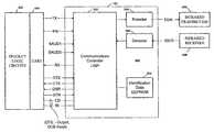
- FIG. 4illustrates a schematic functional block diagram of an IrDA compliant system comprising device logic circuits, the IrDA compliant communications controller depicted in FIG. 3 and an infrared transmitter and receiver.
- the present inventionis directed to a method, system and apparatus for programming and supplying a unique identification data string in combination with a communications controller.
- an IrDA compliant communications controlleris adapted for storing an identification string in an electrically erasable and programmable read only memory (EEPROM).
- the communications controllermay have an initial generic identification string programmed at the time of manufacture and may subsequently, either before or after shipment from the place of manufacture, have a more specific (unique) identification string programmed so as to more readily and fully identify the IRDA compliant device type, features and other parameters unique to that device in which the communications controller is integrated. It is contemplated and within the scope of the present invention that a unique identification data string may be used in combination with communications controllers adapted for any type of wired or wireless communications protocol.
- a communications controller 102 in combination with an identification data memory 104provides a device 106 with a unique identification data string.
- a plurality of devices 106 a and 106 bmay be in communications through associated communications controllers 102 a and 102 b, respectively, over a data communications link 108 .
- the data communications link 108may be either a wired communications circuit, e.g., Ethernet, USB, DALI, LIN, J-1850, IEEE-1451, Firewire, etc., or a wireless communications circuit, e.g., IrDA, Bluetooth, etc.
- an associated identification memory 104 a and 104 bmay store either a generic or unique identification data string for each of the devices 106 a and 106 b, respectively.
- the identification data string(generic or unique) may be easily programmed at any time before, during or after manufacture of the device.
- the IrDA compliant communications controlleris generally represented by the numeral 102 and comprises a processor and arithmetic logic unit (ALU) 206 , a random access memory (RAM) 208 , a program memory 210 , an identification data electrically erasable and programmable read only memory (EEPROM) 204 , a data and address bus 212 , a first port input-output (I/O) 214 , a second port input-output (I/O) 216 , a power-up timer 218 , a timing generator 220 and a power-on reset 222 .
- ALUarithmetic logic unit
- RAMrandom access memory
- EEPROMelectrically erasable and programmable read only memory
- the communications controller 102may be adapted for Data Terminal Equipment (DTE) or for Data Communication Equipment (DCE). Functional operation of the signals at the I/O ports 214 and 216 are more fully described in Table 1 for DTE and Table 2 for DCE.
- DTEData Terminal Equipment
- DCEData Communication Equipment
- TABLE 1 (DTE) PIN PIN BUFFER NAME TYPE TYPE DESCRIPTION BAUD0 I ST BAUD1:BAUD0specifies the Baud rate of the device.
- TXIR OAsynchronous transmit to IrDA transceiver RXIR I ST Asynchronous receive from IrDA transceiver RESET I ST Resets the Device V SS — P Ground reference for logic and I/O Pins EN I TTL Device Enable. May be used in low power and sleep modes
- DSR OData Set Ready.
- TXIR OAsynchronous transmit to IrDA transceiver RXIR I ST Asynchronous receive from IrDA transceiver RESET I ST Resets the Device V SS — P Ground reference for logic and I/O Pins EN I TTL Device Enable. May be used in low power and sleep modes
- TX I TTLAsynchronous receive; from Host Controller UART RX O — Asynchronous transmit; to Host Controller UART RI I TTL Ring Indicator. The status of this bit is passed back to the IrDA Primary Device.
- DSR OData Set Ready.
- the communications controller 102functionally comprises communications controller logic 302 , an encoder 304 , a decoder 306 and the identification data EEPROM 204 .
- the encoder 304 and decoder 306may comprise a combination of hardware logic and software program instructions.
- the exemplary embodiment of the communications controller 102may be fabricated on a semiconductor integrated circuit 308 .
- the identification data EEPROM 204is adapted to store the identification string for the IrDA compliant device.
- the EEPROM 204may be programmed at any time for a unique identification string. Initially a generic identification string may be programmed, but once the intended IrDA compliant device is know, or when the communications controller 102 is embedded in a specific IrDA compliant device, the identification string may be easily programmed in the EEPROM 204 with the desired unique identification information.
- FIG. 4a schematic functional block diagram of an IrDA compliant system comprising IrDA compliant device logic circuits 402 and a UART 404 , the communications controller 102 depicted in FIG. 2, and an infrared transmitter 406 and an infrared receiver 408 .
- the communications controller 102is connected between the infrared transmitter 406 and receiver 408 (optical transceiver) and a device 106 (see FIG. 1) comprising the product logic circuits 402 and the UART 404 .
- the product logic circuits 302may be part of an IrDA compliant device, e.g., printer, video camera, PDA, wireless keyboard, wireless mouse, etc.
- the communications controller 102in combination with the infrared transmitter 406 and receiver 408 , gives the product IrDA compliant capabilities.
- the identification data EEPROM 204supplies the communications controller 102 with the identification string (generic or unique).
- the UART 404sends transmit serial data (TX) to an input of the encoder 304 .
- the encode 304encodes the transmit serial data into transmit electrical pulses (TXIR) compatible with IR light transmission.
- TXIR pulsesare coupled to the IR transmitter 406 for transmission by IR light pulses.
- the BAUD rate of the light pulsesis determined by the communication controller logic 302 (inputs BAUDI and BAUDO).
- IR light pulsesare received and by the IR optical receiver 408 . These received IR light pulses are detected by the IR optical receiver 408 and converted into receive electrical pulses (RXIR) which are coupled to the decoder 306 .
- the decoder 306decodes the received electrical pulses (RXIR) into receive serial data (RX) and formats the receive serial data (RX) to the communications controller logic 302 which sends the RX signals to the UART 404 .
- the product logic circuits 402may be any type of digital circuit having serial digital data communications capabilities, e.g., a microcomputer with a UART 404 , a central processing unit (CPU) and UART, a reduced instruction set computer (RISC) or complex instruction set computer (CISC) and a UART, a digital signal processor with a UART, and the like.
- a microcomputer with a UART 404e.g., a microcomputer with a UART 404 , a central processing unit (CPU) and UART, a reduced instruction set computer (RISC) or complex instruction set computer (CISC) and a UART, a digital signal processor with a UART, and the like.
- RISCreduced instruction set computer
- CISCcomplex instruction set computer
- the present inventionmay function so as to accommodate an infrared standard such as Infrared Data Association (IrDA) Serial Physical Layer Specification, version 1.3 (Oct. 15, 1998) and IrDA Control Specification, final revision (Jun. 30, 1998), both IrDA standards being incorporated by reference herein for all purposes.
- IrDAInfrared Data Association
- Serial Physical Layer Specificationversion 1.3
- IrDA Control Specificationfinal revision
Landscapes
- Engineering & Computer Science (AREA)
- Databases & Information Systems (AREA)
- Computer Networks & Wireless Communication (AREA)
- Signal Processing (AREA)
- Communication Control (AREA)
Abstract
Description
| TABLE 1 |
| (DTE) |
| PIN | PIN | BUFFER | |
| NAME | TYPE | TYPE | DESCRIPTION |
| BAUD0 | I | ST | BAUD1:BAUD0 specifies the Baud rate |
| of the device. | |||
| TXIR | O | — | Asynchronous transmit to IrDA |
| transceiver | |||
| RXIR | I | ST | Asynchronous receive from IrDA |
| transceiver | |||
| RESET | I | ST | Resets the Device |
| VSS | — | P | Ground reference for logic and I/O Pins |
| EN | I | TTL | Device Enable. May be used in low power |
| and sleep modes | |||
| TX | I | TTL | Asynchronous receive; from Host |
| Controller UART | |||
| RX | O | — | Asynchronous transmit; to Host Controller |
| UART | |||
| RI | O | — | Ring Indicator. The value on this pin is |
| driven high. | |||
| DSR | O | — | Data Set Ready. Indicates that the host |
| controller has completed reset. | |||
| DTR | I | TTL | Data Terminal Ready. The value on this |
| pin is ignored. | |||
| CTS | O | — | Clear to Send. Indicates that the host |
| controller is ready to receive data. | |||
| RTS | I | TTL | Request to Send. Indicates that a Host |
| Controller is ready to receive, and that the | |||
| host controller must prepare send data if | |||
| available. | |||
| VDD | — | P | Positive supply for logic and I/O pins |
| OSC2 | O | — | Oscillator crystal Output |
| OSC1/ | I | CMOS | Oscillator crystal input/external clock |
| CLKIN | source input | ||
| CD | O | — | Carrier Detect. Indicates that the host |
| controller has established a valid IrDA | |||
| link with a Primary Device. | |||
| BAUD1 | I | ST | BAUD1:BAUD0 specify the Baud rate of |
| the device. | |||
| TABLE 2 |
| (DCE) |
| PIN | PIN | BUFFER | |
| NAME | TYPE | TYPE | DESCRIPTION |
| BAUD0 | I | ST | BAUD1:BAUD0 specify the Baud rate of |
| the device. | |||
| TXIR | O | — | Asynchronous transmit to IrDA |
| transceiver | |||
| RXIR | I | ST | Asynchronous receive from IrDA |
| transceiver | |||
| RESET | I | ST | Resets the Device |
| VSS | — | P | Ground reference for logic and I/O Pins |
| EN | I | TTL | Device Enable. May be used in low power |
| and sleep modes | |||
| TX | I | TTL | Asynchronous receive; from Host |
| Controller UART | |||
| RX | O | — | Asynchronous transmit; to Host Controller |
| UART | |||
| RI | I | TTL | Ring Indicator. The status of this bit is |
| passed back to the IrDA Primary Device. | |||
| DSR | O | — | Data Set Ready. Indicates that the host |
| controller has established a valid IrDA | |||
| link with a Primary Device.(2) | |||
| DTR | I | TTL | Data Terminal Ready. The status of this |
| bit is passed back to the IrDA Primary | |||
| Device. | |||
| CTS | O | — | Clear to Send. Indicates that the host |
| controller is ready to receive data. | |||
| RTS | I | TTL | Request to Send. Indicates that a Host |
| Controller is ready to receive, and that | |||
| the host controller must prepare send data | |||
| is available. | |||
| VDD | — | P | Positive supply for logic and I/O pins |
| OSC2 | O | — | Oscillator crystal Output |
| OSC1/ | I | CMOS | Oscillator crystal input/external clock |
| CLKIN | source input | ||
| CD | I | ST | Carrier Detect. The status of this bit is |
| passed back to the IrDA Primary Device. | |||
| BAUD1 | I | ST | BAUD1:BAUD0 specify the Baud rate of |
| the device. | |||
| Legend: | |||
| TTL = TTL compatible input | |||
| I = Input | |||
| P = Power | |||
| ST = Schmitt Trigger input with CMOS levels | |||
| O = Output | |||
| CMOS = CMOS compatible input | |||
Claims (4)
Priority Applications (1)
| Application Number | Priority Date | Filing Date | Title |
|---|---|---|---|
| US09/866,991US6810435B2 (en) | 2001-05-29 | 2001-05-29 | Programmable identification in a communications controller |
Applications Claiming Priority (1)
| Application Number | Priority Date | Filing Date | Title |
|---|---|---|---|
| US09/866,991US6810435B2 (en) | 2001-05-29 | 2001-05-29 | Programmable identification in a communications controller |
Publications (2)
| Publication Number | Publication Date |
|---|---|
| US20030016419A1 US20030016419A1 (en) | 2003-01-23 |
| US6810435B2true US6810435B2 (en) | 2004-10-26 |
Family
ID=25348862
Family Applications (1)
| Application Number | Title | Priority Date | Filing Date |
|---|---|---|---|
| US09/866,991Expired - LifetimeUS6810435B2 (en) | 2001-05-29 | 2001-05-29 | Programmable identification in a communications controller |
Country Status (1)
| Country | Link |
|---|---|
| US (1) | US6810435B2 (en) |
Cited By (11)
| Publication number | Priority date | Publication date | Assignee | Title |
|---|---|---|---|---|
| US20030223281A1 (en)* | 2002-05-29 | 2003-12-04 | Micron Technology, Inc. | Programable identification circuitry |
| US20050030375A1 (en)* | 2001-11-09 | 2005-02-10 | Giovanni Zangrande | Image capture device with multiple protocol wireless transmission |
| US20050037665A1 (en)* | 2003-07-03 | 2005-02-17 | Autonetworks Technologies, Ltd. | Conductive path |
| US7007118B2 (en)* | 2003-03-21 | 2006-02-28 | Industrial Technology Research Institute | Computer system for integrating car electronic devices |
| US20070083584A1 (en)* | 2005-09-15 | 2007-04-12 | Dybsetter Gerald L | Integrated multiply and divide circuit |
| US20090309512A1 (en)* | 2006-07-20 | 2009-12-17 | Gotthard Schleicher | Switchegear, system for controlling a lamp, and light control system for a building comprising at least one light |
| US8065443B1 (en)* | 2005-05-20 | 2011-11-22 | Intermec Ip Corp | Computerized device for data collection and communication |
| US20140075069A1 (en)* | 2012-09-07 | 2014-03-13 | Apple Inc. | Data structures for facilitating communication between a host device and an accessory |
| US9307312B2 (en) | 2013-03-15 | 2016-04-05 | Apple Inc. | Audio accessory with internal clock |
| US12186241B2 (en) | 2021-01-22 | 2025-01-07 | Hill-Rom Services, Inc. | Time-based wireless pairing between a medical device and a wall unit |
| US12279999B2 (en) | 2021-01-22 | 2025-04-22 | Hill-Rom Services, Inc. | Wireless configuration and authorization of a wall unit that pairs with a medical device |
Families Citing this family (9)
| Publication number | Priority date | Publication date | Assignee | Title |
|---|---|---|---|---|
| JP4420647B2 (en)* | 2003-04-15 | 2010-02-24 | シャープ株式会社 | Control system |
| WO2005022692A2 (en) | 2003-08-21 | 2005-03-10 | Hill-Rom Services, Inc. | Plug and receptacle having wired and wireless coupling |
| US7884735B2 (en)* | 2005-02-11 | 2011-02-08 | Hill-Rom Services, Inc. | Transferable patient care equipment support |
| US7643850B2 (en)* | 2005-10-11 | 2010-01-05 | Sony Ericsson Mobile Communications Ab | Cellular communication terminals and methods that sense terminal movement for cursor control |
| US7616186B2 (en)* | 2005-12-09 | 2009-11-10 | Sony Ericsson Mobile Communications Ab | Acceleration reference devices, cellular communication terminal systems, and methods that sense terminal movement for cursor control |
| US7835806B2 (en)* | 2007-01-29 | 2010-11-16 | Rockwell Automation Technologies, Inc. | Method for indirect access to controller data using name stored in string tag |
| US8233215B2 (en)* | 2009-08-18 | 2012-07-31 | Ciena Corporation | Optical module manufacturing and testing systems and methods |
| US9915939B2 (en)* | 2013-12-13 | 2018-03-13 | General Electric Company | Systems and methods for providing multiple frame rates on a common physical network |
| US10395769B2 (en) | 2015-12-16 | 2019-08-27 | Hill-Rom Services, Inc. | Patient care devices with local indication of correspondence and power line interconnectivity |
Citations (4)
| Publication number | Priority date | Publication date | Assignee | Title |
|---|---|---|---|---|
| US5444439A (en)* | 1988-09-27 | 1995-08-22 | Matsushita Electric Works, Ltd. | Data setting system for terminal units in remote supervisory and controlling system employing data transmission |
| US5734487A (en)* | 1994-06-30 | 1998-03-31 | Compaq Computer Corporation | Computer system incorporating an infrared link for reduced interference communication with a radio transceiver |
| US5812293A (en)* | 1996-12-31 | 1998-09-22 | Yen; Kerl | A/V signal transmission remote control system |
| US5850304A (en)* | 1997-01-08 | 1998-12-15 | Scottsdale Technologies, Inc. | Optically programmable controller |
- 2001
- 2001-05-29USUS09/866,991patent/US6810435B2/ennot_activeExpired - Lifetime
Patent Citations (4)
| Publication number | Priority date | Publication date | Assignee | Title |
|---|---|---|---|---|
| US5444439A (en)* | 1988-09-27 | 1995-08-22 | Matsushita Electric Works, Ltd. | Data setting system for terminal units in remote supervisory and controlling system employing data transmission |
| US5734487A (en)* | 1994-06-30 | 1998-03-31 | Compaq Computer Corporation | Computer system incorporating an infrared link for reduced interference communication with a radio transceiver |
| US5812293A (en)* | 1996-12-31 | 1998-09-22 | Yen; Kerl | A/V signal transmission remote control system |
| US5850304A (en)* | 1997-01-08 | 1998-12-15 | Scottsdale Technologies, Inc. | Optically programmable controller |
Cited By (18)
| Publication number | Priority date | Publication date | Assignee | Title |
|---|---|---|---|---|
| US20050030375A1 (en)* | 2001-11-09 | 2005-02-10 | Giovanni Zangrande | Image capture device with multiple protocol wireless transmission |
| US7471535B2 (en) | 2002-05-29 | 2008-12-30 | Micron Technology, Inc. | Programable identification circuitry |
| US20030223281A1 (en)* | 2002-05-29 | 2003-12-04 | Micron Technology, Inc. | Programable identification circuitry |
| US7046536B2 (en)* | 2002-05-29 | 2006-05-16 | Micron Technology, Inc. | Programable identification circuitry |
| US20060158916A1 (en)* | 2002-05-29 | 2006-07-20 | Micron Technology, Inc. | Programable identification circuitry |
| US7007118B2 (en)* | 2003-03-21 | 2006-02-28 | Industrial Technology Research Institute | Computer system for integrating car electronic devices |
| US7118415B2 (en)* | 2003-07-03 | 2006-10-10 | Autonetworks Technologies, Ltd. | Conductive path |
| US20050037665A1 (en)* | 2003-07-03 | 2005-02-17 | Autonetworks Technologies, Ltd. | Conductive path |
| US8065443B1 (en)* | 2005-05-20 | 2011-11-22 | Intermec Ip Corp | Computerized device for data collection and communication |
| US20070083584A1 (en)* | 2005-09-15 | 2007-04-12 | Dybsetter Gerald L | Integrated multiply and divide circuit |
| US8930434B2 (en)* | 2005-09-15 | 2015-01-06 | Finisar Corporation | Integrated multiply and divide circuit |
| US8129921B2 (en)* | 2006-07-20 | 2012-03-06 | Osram Ag | Switchegear, system for controlling a lamp, and light control system for a building comprising at least one light |
| US20090309512A1 (en)* | 2006-07-20 | 2009-12-17 | Gotthard Schleicher | Switchegear, system for controlling a lamp, and light control system for a building comprising at least one light |
| US20140075069A1 (en)* | 2012-09-07 | 2014-03-13 | Apple Inc. | Data structures for facilitating communication between a host device and an accessory |
| US9223742B2 (en)* | 2012-09-07 | 2015-12-29 | Apple Inc. | Data structures for facilitating communication between a host device and an accessory |
| US9307312B2 (en) | 2013-03-15 | 2016-04-05 | Apple Inc. | Audio accessory with internal clock |
| US12186241B2 (en) | 2021-01-22 | 2025-01-07 | Hill-Rom Services, Inc. | Time-based wireless pairing between a medical device and a wall unit |
| US12279999B2 (en) | 2021-01-22 | 2025-04-22 | Hill-Rom Services, Inc. | Wireless configuration and authorization of a wall unit that pairs with a medical device |
Also Published As
| Publication number | Publication date |
|---|---|
| US20030016419A1 (en) | 2003-01-23 |
Similar Documents
| Publication | Publication Date | Title |
|---|---|---|
| US6810435B2 (en) | Programmable identification in a communications controller | |
| US5537558A (en) | Apparatus and method for communicating multiple devices through one PCMCIA interface | |
| US10937020B2 (en) | Wearable device with near-field communication function and near-field communication control system | |
| CN112514332B (en) | Method and system for switching USB (universal serial bus) device to internet of things (IoT) device to operate based on thing description model | |
| KR19990087498A (en) | One-Wire Universal Asynchronous Transceiver (UART) for Processor Systems | |
| WO2014154151A1 (en) | System and method for secure pairing of bluetooth devices | |
| US12166540B2 (en) | Exchange of data between a NFC reader and a dual NFC interface transponder | |
| US20020176138A1 (en) | Infrared encoder/decoder having hardware and software data rate selection | |
| US12229063B2 (en) | Method of storing instructions in program memory and associated system | |
| JP5985299B2 (en) | Electronic device, control device and network system | |
| US7850082B1 (en) | Extended universal serial bus (USB) card reader | |
| CN110704341A (en) | Device and method for upgrading code by serial port single line | |
| CN114759942A (en) | Chip and data conversion method | |
| US20180329846A1 (en) | Inter-device digital audio | |
| KR20090071918A (en) | How to set parameters in the PSI network | |
| WO2002009405A2 (en) | Universal serial bus datapump command interpreter | |
| US20040252649A1 (en) | Dual mode wireless network card link parameter setting device and method of the same | |
| US8427357B2 (en) | Remote control system and method for operating the same | |
| KR100446427B1 (en) | Remote inspection apparatus installed between host computer and meter | |
| KR200221933Y1 (en) | Wire and wireless interfacing apparatus for computer | |
| US12216952B2 (en) | Method for printing a Zigbee install code and corresponding systems and devices | |
| US20060197675A1 (en) | Remote control interface framework using an infrared module and a method thereof | |
| CN213718228U (en) | Bluetooth module | |
| US11677444B2 (en) | Contactless transponder and method | |
| EP4068107B1 (en) | Audio control circuit, host device and associated control method |
Legal Events
| Date | Code | Title | Description |
|---|---|---|---|
| AS | Assignment | Owner name:MICROCHIP TECHNOLOGY INCORPORATED, ARIZONA Free format text:ASSIGNMENT OF ASSIGNORS INTEREST;ASSIGNORS:PALMER, MARK;SCHLANGER, STEVEN ERIC;REEL/FRAME:012218/0319;SIGNING DATES FROM 20010920 TO 20010925 Owner name:AEGIS TECHNOLOGIES, L.L.C., ARIZONA Free format text:ASSIGNMENT OF ASSIGNORS INTEREST;ASSIGNORS:PALMER, MARK;SCHLANGER, STEVEN ERIC;REEL/FRAME:012218/0319;SIGNING DATES FROM 20010920 TO 20010925 | |
| STCF | Information on status: patent grant | Free format text:PATENTED CASE | |
| FPAY | Fee payment | Year of fee payment:4 | |
| REMI | Maintenance fee reminder mailed | ||
| FPAY | Fee payment | Year of fee payment:8 | |
| FPAY | Fee payment | Year of fee payment:12 | |
| AS | Assignment | Owner name:JPMORGAN CHASE BANK, N.A., AS ADMINISTRATIVE AGENT, DELAWARE Free format text:SECURITY INTEREST;ASSIGNORS:MICROCHIP TECHNOLOGY INC.;SILICON STORAGE TECHNOLOGY, INC.;ATMEL CORPORATION;AND OTHERS;REEL/FRAME:053311/0305 Effective date:20200327 | |
| AS | Assignment | Owner name:SILICON STORAGE TECHNOLOGY, INC., ARIZONA Free format text:RELEASE BY SECURED PARTY;ASSIGNOR:JPMORGAN CHASE BANK, N.A, AS ADMINISTRATIVE AGENT;REEL/FRAME:053466/0011 Effective date:20200529 Owner name:MICROSEMI CORPORATION, CALIFORNIA Free format text:RELEASE BY SECURED PARTY;ASSIGNOR:JPMORGAN CHASE BANK, N.A, AS ADMINISTRATIVE AGENT;REEL/FRAME:053466/0011 Effective date:20200529 Owner name:MICROCHIP TECHNOLOGY INC., ARIZONA Free format text:RELEASE BY SECURED PARTY;ASSIGNOR:JPMORGAN CHASE BANK, N.A, AS ADMINISTRATIVE AGENT;REEL/FRAME:053466/0011 Effective date:20200529 Owner name:MICROSEMI STORAGE SOLUTIONS, INC., ARIZONA Free format text:RELEASE BY SECURED PARTY;ASSIGNOR:JPMORGAN CHASE BANK, N.A, AS ADMINISTRATIVE AGENT;REEL/FRAME:053466/0011 Effective date:20200529 Owner name:ATMEL CORPORATION, ARIZONA Free format text:RELEASE BY SECURED PARTY;ASSIGNOR:JPMORGAN CHASE BANK, N.A, AS ADMINISTRATIVE AGENT;REEL/FRAME:053466/0011 Effective date:20200529 | |
| AS | Assignment | Owner name:WELLS FARGO BANK, NATIONAL ASSOCIATION, MINNESOTA Free format text:SECURITY INTEREST;ASSIGNORS:MICROCHIP TECHNOLOGY INC.;SILICON STORAGE TECHNOLOGY, INC.;ATMEL CORPORATION;AND OTHERS;REEL/FRAME:053468/0705 Effective date:20200529 | |
| AS | Assignment | Owner name:WELLS FARGO BANK, NATIONAL ASSOCIATION, AS COLLATERAL AGENT, MINNESOTA Free format text:SECURITY INTEREST;ASSIGNORS:MICROCHIP TECHNOLOGY INCORPORATED;SILICON STORAGE TECHNOLOGY, INC.;ATMEL CORPORATION;AND OTHERS;REEL/FRAME:055671/0612 Effective date:20201217 | |
| AS | Assignment | Owner name:WELLS FARGO BANK, NATIONAL ASSOCIATION, AS NOTES COLLATERAL AGENT, MINNESOTA Free format text:SECURITY INTEREST;ASSIGNORS:MICROCHIP TECHNOLOGY INCORPORATED;SILICON STORAGE TECHNOLOGY, INC.;ATMEL CORPORATION;AND OTHERS;REEL/FRAME:057935/0474 Effective date:20210528 | |
| AS | Assignment | Owner name:MICROSEMI STORAGE SOLUTIONS, INC., ARIZONA Free format text:RELEASE BY SECURED PARTY;ASSIGNOR:WELLS FARGO BANK, NATIONAL ASSOCIATION, AS NOTES COLLATERAL AGENT;REEL/FRAME:059863/0400 Effective date:20220228 Owner name:MICROSEMI CORPORATION, ARIZONA Free format text:RELEASE BY SECURED PARTY;ASSIGNOR:WELLS FARGO BANK, NATIONAL ASSOCIATION, AS NOTES COLLATERAL AGENT;REEL/FRAME:059863/0400 Effective date:20220228 Owner name:ATMEL CORPORATION, ARIZONA Free format text:RELEASE BY SECURED PARTY;ASSIGNOR:WELLS FARGO BANK, NATIONAL ASSOCIATION, AS NOTES COLLATERAL AGENT;REEL/FRAME:059863/0400 Effective date:20220228 Owner name:SILICON STORAGE TECHNOLOGY, INC., ARIZONA Free format text:RELEASE BY SECURED PARTY;ASSIGNOR:WELLS FARGO BANK, NATIONAL ASSOCIATION, AS NOTES COLLATERAL AGENT;REEL/FRAME:059863/0400 Effective date:20220228 Owner name:MICROCHIP TECHNOLOGY INCORPORATED, ARIZONA Free format text:RELEASE BY SECURED PARTY;ASSIGNOR:WELLS FARGO BANK, NATIONAL ASSOCIATION, AS NOTES COLLATERAL AGENT;REEL/FRAME:059863/0400 Effective date:20220228 | |
| AS | Assignment | Owner name:MICROSEMI STORAGE SOLUTIONS, INC., ARIZONA Free format text:RELEASE BY SECURED PARTY;ASSIGNOR:WELLS FARGO BANK, NATIONAL ASSOCIATION, AS NOTES COLLATERAL AGENT;REEL/FRAME:059363/0001 Effective date:20220228 Owner name:MICROSEMI CORPORATION, ARIZONA Free format text:RELEASE BY SECURED PARTY;ASSIGNOR:WELLS FARGO BANK, NATIONAL ASSOCIATION, AS NOTES COLLATERAL AGENT;REEL/FRAME:059363/0001 Effective date:20220228 Owner name:ATMEL CORPORATION, ARIZONA Free format text:RELEASE BY SECURED PARTY;ASSIGNOR:WELLS FARGO BANK, NATIONAL ASSOCIATION, AS NOTES COLLATERAL AGENT;REEL/FRAME:059363/0001 Effective date:20220228 Owner name:SILICON STORAGE TECHNOLOGY, INC., ARIZONA Free format text:RELEASE BY SECURED PARTY;ASSIGNOR:WELLS FARGO BANK, NATIONAL ASSOCIATION, AS NOTES COLLATERAL AGENT;REEL/FRAME:059363/0001 Effective date:20220228 Owner name:MICROCHIP TECHNOLOGY INCORPORATED, ARIZONA Free format text:RELEASE BY SECURED PARTY;ASSIGNOR:WELLS FARGO BANK, NATIONAL ASSOCIATION, AS NOTES COLLATERAL AGENT;REEL/FRAME:059363/0001 Effective date:20220228 | |
| AS | Assignment | Owner name:MICROSEMI STORAGE SOLUTIONS, INC., ARIZONA Free format text:RELEASE BY SECURED PARTY;ASSIGNOR:WELLS FARGO BANK, NATIONAL ASSOCIATION, AS NOTES COLLATERAL AGENT;REEL/FRAME:060894/0437 Effective date:20220228 Owner name:MICROSEMI CORPORATION, ARIZONA Free format text:RELEASE BY SECURED PARTY;ASSIGNOR:WELLS FARGO BANK, NATIONAL ASSOCIATION, AS NOTES COLLATERAL AGENT;REEL/FRAME:060894/0437 Effective date:20220228 Owner name:ATMEL CORPORATION, ARIZONA Free format text:RELEASE BY SECURED PARTY;ASSIGNOR:WELLS FARGO BANK, NATIONAL ASSOCIATION, AS NOTES COLLATERAL AGENT;REEL/FRAME:060894/0437 Effective date:20220228 Owner name:SILICON STORAGE TECHNOLOGY, INC., ARIZONA Free format text:RELEASE BY SECURED PARTY;ASSIGNOR:WELLS FARGO BANK, NATIONAL ASSOCIATION, AS NOTES COLLATERAL AGENT;REEL/FRAME:060894/0437 Effective date:20220228 Owner name:MICROCHIP TECHNOLOGY INCORPORATED, ARIZONA Free format text:RELEASE BY SECURED PARTY;ASSIGNOR:WELLS FARGO BANK, NATIONAL ASSOCIATION, AS NOTES COLLATERAL AGENT;REEL/FRAME:060894/0437 Effective date:20220228 |