US6809766B1 - Look ahead rolling shutter system in CMOS sensors - Google Patents
Look ahead rolling shutter system in CMOS sensorsDownload PDFInfo
- Publication number
- US6809766B1 US6809766B1US09/773,400US77340001AUS6809766B1US 6809766 B1US6809766 B1US 6809766B1US 77340001 AUS77340001 AUS 77340001AUS 6809766 B1US6809766 B1US 6809766B1
- Authority
- US
- United States
- Prior art keywords
- reset
- pointer
- shift register
- exposure time
- read
- Prior art date
- Legal status (The legal status is an assumption and is not a legal conclusion. Google has not performed a legal analysis and makes no representation as to the accuracy of the status listed.)
- Expired - Lifetime, expires
Links
- 238000005096rolling processMethods0.000titleclaimsdescription9
- 238000003860storageMethods0.000claimsdescription10
- 230000010354integrationEffects0.000description20
- 238000000034methodMethods0.000description12
- 238000010586diagramMethods0.000description6
- 238000009792diffusion processMethods0.000description4
- 230000008901benefitEffects0.000description3
- 238000005516engineering processMethods0.000description3
- 239000000872bufferSubstances0.000description2
- 239000000969carrierSubstances0.000description2
- 238000004458analytical methodMethods0.000description1
- 230000003139buffering effectEffects0.000description1
- 230000000295complement effectEffects0.000description1
- 230000000694effectsEffects0.000description1
- 230000006870functionEffects0.000description1
- 230000000977initiatory effectEffects0.000description1
- 238000004519manufacturing processMethods0.000description1
- 238000005259measurementMethods0.000description1
- 229910044991metal oxideInorganic materials0.000description1
- 150000004706metal oxidesChemical class0.000description1
- 238000004377microelectronicMethods0.000description1
- 108091008695photoreceptorsProteins0.000description1
- 238000009738saturatingMethods0.000description1
- 239000004065semiconductorSubstances0.000description1
Images


Classifications
- H—ELECTRICITY
- H04—ELECTRIC COMMUNICATION TECHNIQUE
- H04N—PICTORIAL COMMUNICATION, e.g. TELEVISION
- H04N25/00—Circuitry of solid-state image sensors [SSIS]; Control thereof
- H04N25/50—Control of the SSIS exposure
- H04N25/53—Control of the integration time
- H04N25/531—Control of the integration time by controlling rolling shutters in CMOS SSIS
- H—ELECTRICITY
- H04—ELECTRIC COMMUNICATION TECHNIQUE
- H04N—PICTORIAL COMMUNICATION, e.g. TELEVISION
- H04N23/00—Cameras or camera modules comprising electronic image sensors; Control thereof
- H04N23/70—Circuitry for compensating brightness variation in the scene
- H04N23/73—Circuitry for compensating brightness variation in the scene by influencing the exposure time
- H—ELECTRICITY
- H04—ELECTRIC COMMUNICATION TECHNIQUE
- H04N—PICTORIAL COMMUNICATION, e.g. TELEVISION
- H04N25/00—Circuitry of solid-state image sensors [SSIS]; Control thereof
- H04N25/70—SSIS architectures; Circuits associated therewith
- H04N25/76—Addressed sensors, e.g. MOS or CMOS sensors
- H—ELECTRICITY
- H04—ELECTRIC COMMUNICATION TECHNIQUE
- H04N—PICTORIAL COMMUNICATION, e.g. TELEVISION
- H04N25/00—Circuitry of solid-state image sensors [SSIS]; Control thereof
- H04N25/70—SSIS architectures; Circuits associated therewith
- H04N25/76—Addressed sensors, e.g. MOS or CMOS sensors
- H04N25/77—Pixel circuitry, e.g. memories, A/D converters, pixel amplifiers, shared circuits or shared components
- H—ELECTRICITY
- H04—ELECTRIC COMMUNICATION TECHNIQUE
- H04N—PICTORIAL COMMUNICATION, e.g. TELEVISION
- H04N25/00—Circuitry of solid-state image sensors [SSIS]; Control thereof
- H04N25/70—SSIS architectures; Circuits associated therewith
- H04N25/76—Addressed sensors, e.g. MOS or CMOS sensors
- H04N25/7795—Circuitry for generating timing or clock signals
- H—ELECTRICITY
- H04—ELECTRIC COMMUNICATION TECHNIQUE
- H04N—PICTORIAL COMMUNICATION, e.g. TELEVISION
- H04N25/00—Circuitry of solid-state image sensors [SSIS]; Control thereof
- H04N25/70—SSIS architectures; Circuits associated therewith
- H04N25/76—Addressed sensors, e.g. MOS or CMOS sensors
- H04N25/78—Readout circuits for addressed sensors, e.g. output amplifiers or A/D converters
Definitions
- This specificationgenerally relates to a CMOS sensor, and more particularly to a look-ahead shutter system in such a sensor.
- Complementary metal-oxide semiconductor (CMOS) active pixel sensor (APS) technologyis an integrated circuit technology for electronically capturing images, therefore forming an “electronic film.” Unlike charge-coupled device (CCD) image sensors that have been used in the past to capture electronic images, the CMOS sensors use mainstream microelectronic fabrication processes to produce the sensor chips.
- CCDcharge-coupled device
- the advantages of the CMOS APS technologyare low cost, small size, and have an ability to integrate a significant amount of very-large-scale-integrated (VLSI) electronics on-chip.
- each pixel of an image sensor arrayhas both a photodetector and an active transistor circuitry for readout of the pixel signal.
- the photodetector for each pixel in the image sensor arrayconverts photons impinging on the pixel to an electric charge via the photoelectric effect.
- the chargeis integrated over a period of time that is long enough to collect a detectable amount of charge but short enough to avoid saturating storage elements. This period is analogous to a film exposure time (i.e. the shutter speed) and is called an integration time.
- the integration timeis the time between a reset of a given row and a subsequent read of the row.
- the reset/read routineis sequential (i.e. row by row). This routine is referred to as a “rolling electronic shutter.”
- the integration timemay be adjusted by a fixed amount as a result of an image exposure analysis using an average intensity scheme or image histogram measurements.
- the shutter widthis the time between integration enable and readout. This may be of any size depending on the number of adjacent pixels that will have the same integration time.
- the shutter widthmay also be adjusted by a fixed value to control the gain of an exposed area of a sensor array.
- a particular rowneeds to be accessed at some given time before the readout.
- the accessed rowneeds to be reset to start a new integration.
- a reset pointermoves ahead of a read pointer by an amount equal to the shutter width.
- the time difference between the two pointersis the integration time.
- the integration processmay encounter some difficulties in implementing the change. For example, when the integration time is increased, the reset pointer needs to jump to the beginning of the frame without completing the previous reset cycle. This may be seen as an artifact or a short flash in the bottom portion of the image.
- the present disclosureincludes a shutter system for a pixel array.
- the systemincludes a read shift register, first and second reset shift registers, and a plurality of logic gates.
- the read shift registeris configured to sequentially count rows of the pixel array from top to bottom, such that the read shift register generates a read pointer.
- the first reset shift registeris configured to sequentially reset rows of the pixel array from top to bottom.
- the first reset shift registerprovides a first reset pointer for allowing reset of pixels in a row indicated by the first reset pointer.
- the first reset pointerallows reset of pixels prior to reading of the pixels in a row indicated by the read pointer.
- the time difference between the first reset pointer and the read pointerindicates an exposure time.
- the second reset shift registeris configured to provide a second reset pointer, which enables the first reset shift register to sequentially reset rows of the pixel array without generating any flashes when the exposure time is increased.
- the plurality of logic gatesdirect outputs of the read shift register and the first and second reset shift registers to each pixels in the pixel array.
- FIG. 1shows the system with the shutter closed and the array and the reset stayed.
- FIG. 2shows the start of exposure
- FIG. 3shows the advance of the shutter.
- FIG. 4shows how each row is read into an analog to digital converter and the shutter is closed behind it.
- FIG. 5shows the positions of the read pointer and shutter pointer as the process continues.
- FIG. 6shows the process of selecting a new shutter width in a flowchart.
- FIG. 7shows the first step in a process of changing the exposure.
- FIG. 8shows the shutter conditions at the bottom of that window.
- FIG. 9shows the bottom of the window and the beginning of the next window.
- FIG. 10shows the complete new frame with the set up shutter width.
- FIG. 11shows continuation of the reading.
- FIG. 12shows the new pointer initiating a new shutter width.
- FIG. 13shows the continuation of the reading with both shutters enabled.
- FIG. 14shows the first shutter pointer wrapping around loaded with the second shutter pointer value.
- FIG. 15shows the new frame starting with the updated shutter width.
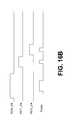
- FIG. 16Aillustrates a circuit realization of a two-pointer reset operation.
- FIG. 16Billustrates timing diagrams of the two-pointer reset operation.
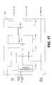
- FIG. 17is a block diagram of a control circuit that performs rolling reset operation.
- the present disclosuredescribes a two-reset pointer rolling shutter system.
- FIG. 1shows a block diagram of the active pixel sensor (APS) array, along with a sample schematic of the way the array may operate. While the system shows a photodiode pixel, it should be understood that the technique applies to any kind of pixel including, for example, a photo-gate pixel or any other photo-receptor.
- APSactive pixel sensor
- the APS array 100When the array is in the reset state, the APS array 100 shows all pixels as being shaded, meaning that all are in the “don't care” state.
- the pixelsare collectively sampled into an A/D converter using a system with a floating diffusion 102 that is sampled into a source follower 104 .
- the output of the source follower 104is also sampled through a row selector transistor 106 onto column bus 108 .
- the column bus 108is coupled into the A/D converter array described herein.
- the shutteris closed and thus the gate 110 is in the reset state.
- the rowis reset by providing a V DD potential on the gate 110 that connects the floating diffusion 102 to a sink well 112 .
- the reset valueis released, the floating diffusion 102 can accumulate charge from incoming photo-carriers.
- the potentials of the various elementsare shown in state diagram 115 : all incoming photo-carriers are sinked to the well 117 .
- the exposurehas been started. This may be done by advancing the shutter counter through the array selectively releasing the array from reset.
- the rate at which the opening is advanced through the arrayis the same as the read row rate.
- the operationoccurs by releasing the reset to each row in a timed manner.
- the timingmay be controlled by a controller that may be dedicated logic or a microprocessor.
- FIG. 2shows how the states change when reset is released. Each floating diffusion begins to integrate charge once released. The read pointer is disabled, to avoid any false reads.
- row 4shown by pointer 200 , is being advanced cyclically. Therefore, row 1 has been opened for the time of 4 clock rate exposures.
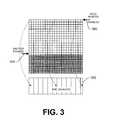
- FIG. 3shows the operation continuing.
- Pointer 200has now reached the 15th row and in this example, we assume that 15 exposure cycles are desired.
- the read pointer 154is enabled; shown as element 300 .
- the enabling of read pointer 300enables the row select 106 and thereby provides the charge from that row onto the column bus 108 into associated A/D converter 302 .
- the first row of the arrayis read into the column processing A/D circuits.
- the shutter advancing speedmatches the row processing speed.
- the shutter widthequals 14 rows and the pixel integration time equals 14 times the process time per row.
- the reset for that particular rowis again brought active to maintain the pixel in reset.
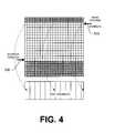
- FIG. 4shows the continuation of the process.
- the read pointer 300is always 15 rows behind the shutter pointer 200 .
- the shutter pointer 200may be referred to as a reset pointer. Each row is read into the A/D converter, and the shutter is closed behind it by bringing the appropriate reset transistor 110 into reset.
- FIG. 5shows the way in which the pointers wrap around.
- the shutter pointerreaches the bottom 500 of the array, it wraps back around to the top 502 of the array.
- the read pointercontinues to read behind the time of the shutter pointer enablement.
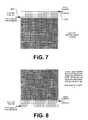
- FIG. 7shows the beginning of a new frame. As shown at 600 in the flowchart of FIG. 6, the shutter pointer 1 is set to the desired width, pointer 2 is disabled, and the read pointer is enabled. The read pointer tells the pixels to be read a specified amount of time after the shutter pointer has enabled them.
- FIG. 7shows the system operating with the current shutter width of three rows.
- FIG. 7shows a new shutter width at 602 .
- the new shutter width in this exampleis 14 rows although it could be any value.
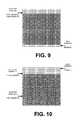
- FIG. 8shows the shutter pointer reaching the bottom of the frame.
- FIG. 9shows the read pointer reaching the bottom of the frame and
- FIG. 10shows the read pointer reaching the top of the frame.
- the shutter pointer 2is set to the new width.
- pointer 2remains disabled at this time and through the subject of FIG. 11 where it moves in step with pointer 1 and the read pointer. This is represented as 606 in FIG. 6 .
- the shutter pointer 2reaches the end of the frame, as detected at 608 and shown in FIGS.
- the read pointer 200is still reading three rows behind the shutter pointer 1 ( 300 ). However, subsequent top rows such as 1200 are being turned on by shutter pointer 2 ( 1202 ). This is shown generally as 610 in FIG. 6 .
- the readscontinue, as shown in FIG. 13 .
- pointer 1reaches the bottom of the frame, 612 in FIG. 14, pointer 1 receives the contents of pointer 2 ( 614 ) and wraps around loaded with the value of pointer 2 ( 1400 ). Therefore, when the read pointer 200 reaches the bottom of the frame, the bottom-most row receives the last three-row exposure.
- the top of the next frameshown in FIG. 15, has a 14-row shutter width.
- FIG. 16Aillustrates a circuit realization of a two-pointer reset operation described above.
- the illustrated embodimentshows a rolling shutter system 1600 having two reset pointers in accordance with an embodiment of the present disclosure.
- the system 1600includes a control circuit 1608 , dynamic shift registers 1602 , 1604 , 1606 , and logic gates 1610 - 1622 that direct the shift register data to pixels in each row.
- the configuration of the system 1600circumvents the need for address calculations.
- the read processstarts with READ_INI signal, from the control circuit 1608 , applied to a read shift register 1602 at the start of a new frame.
- READ_INIBy initializing the read shift register 1602 with READ_INI, the rows are sequentially selected from the top of the frame.
- ROW_EN signalis pulsed (see FIG. 16B) for the duration sufficient to complete the standard pixel read operation, as described above in conjunction with schematic diagrams of FIGS. 1 and 2.
- a pixel resetis performed during this read operation by applying PixRst signal as shown in FIG. 16 B. When both ROW_EN and PixRst signals are at logic high, a given pixel in the selected row is reset.
- the AND gate 1610selectively passes output of the read shift register 1610 during ROW_EN.
- the AND gate 1618allows pixel reset when the PixRst signal is applied during ROW_EN.
- the reset processmay be initiated by either RST_PTR 1 _INI or RST_PTR 2 _INI.
- RST_PTR 1 _INIsignal initializes the first reset shift register 1604
- RST_PTR 2 _INIsignal initializes the second reset shift register 1606 .
- the first reset shift register 1604may be used as a default reset register.
- Pulsing RST 1 _EN signal, and applying PixRst signal through a row driver in the selected rowmay initiate the rolling reset sequence.
- the reset sequencemay be initiated by applying PixRst signal while RST 2 _EN signal is active. See FIG. 16B for the timing details of the above-described sequence.
- the AND gate 1612selectively passes output of the first reset shift register 1604 during RST 1 _EN.
- the AND gate 1614selectively passes output of the second reset shift register 1606 during RST 2 _EN.
- the OR gate 1616provides enabled shift register outputs to the next stage to select or reset a row. Buffers 1620 , 1622 provide buffering of data for row select and reset, respectively. Signals, ROWSEL and RST, are directed to pixels to control the gates as shown in FIGS. 1 and 2.
- a two-pointer reset processmay be started by initializing the second shift register 1606 .
- the processmay be started by initializing the first shift register 1604 when the default reset shift register is the second shift register 1606 .
- the “increase in the integration time” conditionis equivalent to the current reset shift register being in a “busy” condition. If the integration time (i.e. exposure time) is updated incrementally, then the first condition may be easier to implement. If the integration time is programmed, then the second condition may be easier to implement. Either of these conditions may serve as an indicator to alternate the reset shift register. For example, if the first reset shift register 1604 is currently enabled, the first reset shift register 1604 is disabled and the second reset shift register 1606 is enable, and visa versa.
- FIG. 17is a block diagram of a control circuit 1608 that performs rolling reset operation.
- the circuit 1608includes an exposure time register 1700 , a delay counter 1702 , a comparator 1704 , and a multiplexer 1706 .
- the exposure time storage 1700may be programmed, or updated once a frame with an integration time.
- the integration timemay be configured as a row width.
- the storage 1700may include a memory or buffer.
- the storage 1700may include a counter.
- the delay counter 1702operates to start counting from the loaded integration time value until the count has reached a value of one less than the number of rows in a frame (i.e. N ⁇ 1). Since the counter 1702 is load with an integration time value (e.g. shutter width expressed in terms of number of rows) at the beginning of a frame, the delay counter 1702 operates to count rows up to a row that is a shutter width away from the end of the frame, before the reset initialization pulse is issued.
- the comparator 1704performs this task by issuing RST_PTR_INI when it detects that the output of the counter 1702 has reached N ⁇ 1.
- the multiplexer 1706directs the reset initialization pulse, RST_PTR_INI, to either first 1604 or second reset shift register 1606 , depending on which reset shift register was previously enabled. Thus, the multiplexer 1706 operates to alternate the direction of RST_PTR_INI.
- a rowmay be divided into 8 segments, and each of the read pointer and the reset pointers may be updated according to these segments within the row.
Landscapes
- Engineering & Computer Science (AREA)
- Multimedia (AREA)
- Signal Processing (AREA)
- Transforming Light Signals Into Electric Signals (AREA)
- Solid State Image Pick-Up Elements (AREA)
Abstract
Description
Claims (17)
Priority Applications (2)
| Application Number | Priority Date | Filing Date | Title |
|---|---|---|---|
| US09/773,400US6809766B1 (en) | 1998-03-11 | 2001-01-31 | Look ahead rolling shutter system in CMOS sensors |
| US10/958,592US7573516B2 (en) | 1998-03-11 | 2004-10-06 | Look ahead rolling shutter system in CMOS sensors |
Applications Claiming Priority (3)
| Application Number | Priority Date | Filing Date | Title |
|---|---|---|---|
| US09/038,888US6529242B1 (en) | 1998-03-11 | 1998-03-11 | Look ahead shutter pointer allowing real time exposure control |
| US17937800P | 2000-01-31 | 2000-01-31 | |
| US09/773,400US6809766B1 (en) | 1998-03-11 | 2001-01-31 | Look ahead rolling shutter system in CMOS sensors |
Related Parent Applications (1)
| Application Number | Title | Priority Date | Filing Date |
|---|---|---|---|
| US09/038,888Continuation-In-PartUS6529242B1 (en) | 1998-03-11 | 1998-03-11 | Look ahead shutter pointer allowing real time exposure control |
Related Child Applications (1)
| Application Number | Title | Priority Date | Filing Date |
|---|---|---|---|
| US10/958,592ContinuationUS7573516B2 (en) | 1998-03-11 | 2004-10-06 | Look ahead rolling shutter system in CMOS sensors |
Publications (1)
| Publication Number | Publication Date |
|---|---|
| US6809766B1true US6809766B1 (en) | 2004-10-26 |
Family
ID=33161694
Family Applications (2)
| Application Number | Title | Priority Date | Filing Date |
|---|---|---|---|
| US09/773,400Expired - LifetimeUS6809766B1 (en) | 1998-03-11 | 2001-01-31 | Look ahead rolling shutter system in CMOS sensors |
| US10/958,592Expired - LifetimeUS7573516B2 (en) | 1998-03-11 | 2004-10-06 | Look ahead rolling shutter system in CMOS sensors |
Family Applications After (1)
| Application Number | Title | Priority Date | Filing Date |
|---|---|---|---|
| US10/958,592Expired - LifetimeUS7573516B2 (en) | 1998-03-11 | 2004-10-06 | Look ahead rolling shutter system in CMOS sensors |
Country Status (1)
| Country | Link |
|---|---|
| US (2) | US6809766B1 (en) |
Cited By (45)
| Publication number | Priority date | Publication date | Assignee | Title |
|---|---|---|---|---|
| US20030038888A1 (en)* | 2001-08-23 | 2003-02-27 | Flynn David J. | CCD image detector and method of operating the same |
| US20030062582A1 (en)* | 2001-07-20 | 2003-04-03 | Blerkom Daniel Van | Variable pixel clock electronic shutter control |
| US20030193699A1 (en)* | 2001-11-06 | 2003-10-16 | Tay Hiok Nam | Image sensor with time overlapping image output |
| US20030193595A1 (en)* | 2002-04-02 | 2003-10-16 | Stmicroelectronics Ltd | Image sensor with readout circuit |
| US20030202106A1 (en)* | 2002-04-24 | 2003-10-30 | Robert Kandleinsberger | Digital camera with overscan sensor |
| US20040017495A1 (en)* | 2002-07-25 | 2004-01-29 | Fujitsu Limited | Image sensor for suppressing image distortion |
| US20040081446A1 (en)* | 2002-10-28 | 2004-04-29 | Eastman Kodak Company | Electronic imaging system with row-wise or column-wise image sensor reset synchronized to a mechanical shutter |
| US20040201762A1 (en)* | 2003-04-11 | 2004-10-14 | Olympus Corporation | Solid-state imaging apparatus |
| US20050088555A1 (en)* | 2003-01-22 | 2005-04-28 | Masahiro Kanai | Image processing device, image processing method and solid-state image-pickup device |
| US6950131B1 (en)* | 2000-09-26 | 2005-09-27 | Valley Oak Semiconductor | Simultaneous access and reset system for an active pixel sensor |
| US20050265714A1 (en)* | 2004-05-28 | 2005-12-01 | Per Rosdahl | Digital shutter |
| US20060109373A1 (en)* | 2004-11-22 | 2006-05-25 | Seiko Epson Corporation | Imaging device and imaging apparatus |
| US20060238632A1 (en)* | 2005-04-26 | 2006-10-26 | Micron Technology, Inc. | Rolling shutter for prevention of blooming |
| US20070085921A1 (en)* | 2005-10-04 | 2007-04-19 | Kazushi Kitagata | Solid-state imaging device, method of driving solid-state imaging device, and imaging apparatus |
| US20070138293A1 (en)* | 2003-11-13 | 2007-06-21 | Metrologic Instruments, Inc. | Hand-supportable digital image capturing and processing system employing an area-type image sensing array exposed to narrow-band illumination produced from a narrow-band illumination subsystem, transmitted through a narrow-band optical filter structure, and duration-controlled using a photodetector operated independently from said area-type image sensing array |
| US20080030587A1 (en)* | 2006-08-07 | 2008-02-07 | Rene Helbing | Still image stabilization suitable for compact camera environments |
| US20080062293A1 (en)* | 2006-09-08 | 2008-03-13 | Dalsa Corporation | Method for multiphase charge transfer in a lamel shutter and apparatus containing such a shutter |
| US20080129834A1 (en)* | 2006-11-28 | 2008-06-05 | Taner Dosluoglu | Simultaneous global shutter and correlated double sampling read out in multiple photosensor pixels |
| US20080284884A1 (en)* | 2007-05-17 | 2008-11-20 | Sony Corporation | Image sensor, electronic apparatus, and driving method of electronic apparatus |
| US20080284898A1 (en)* | 2002-03-08 | 2008-11-20 | Robert Kandleinsberger | Digital camera |
| US20080291310A1 (en)* | 2007-05-21 | 2008-11-27 | Micron Technology, Inc. | Imager and system utilizing pixel with internal reset control and method of operating same |
| US20080309806A1 (en)* | 2007-06-18 | 2008-12-18 | Canon Kabushiki Kaisha | Imaging system, image sensor, and method of controlling imaging system |
| US20080309810A1 (en)* | 2007-06-15 | 2008-12-18 | Scott Smith | Images with high speed digital frame transfer and frame processing |
| US7490774B2 (en) | 2003-11-13 | 2009-02-17 | Metrologic Instruments, Inc. | Hand-supportable imaging based bar code symbol reader employing automatic light exposure measurement and illumination control subsystem integrated therein |
| US20090073289A1 (en)* | 2006-03-23 | 2009-03-19 | Micron Technology, Inc. | Method and apparatus for providing a rolling double reset timing for global storage in image sensors |
| US20090096890A1 (en)* | 2007-10-16 | 2009-04-16 | Micron Technology, Inc. | Method and apparatus for controlling dual conversion gain signal in imaging devices |
| US7543752B2 (en) | 2003-11-13 | 2009-06-09 | Metrologic Instruments, Inc. | Digital image capture and processing system employing a multi-mode illumination subsystem adaptable to ambient illumination levels |
| US7594609B2 (en) | 2003-11-13 | 2009-09-29 | Metrologic Instruments, Inc. | Automatic digital video image capture and processing system supporting image-processing based code symbol reading during a pass-through mode of system operation at a retail point of sale (POS) station |
| US20100128137A1 (en)* | 2008-11-21 | 2010-05-27 | Eastman Kodak Company | Extended depth of field for image sensor |
| US20100149390A1 (en)* | 2008-12-15 | 2010-06-17 | Altasens, Inc. | Staggered reset in cmos digital sensor device |
| WO2010114594A1 (en) | 2009-04-01 | 2010-10-07 | Eastman Kodak Company | Exposing pixel groups in producing digital images |
| US7841533B2 (en) | 2003-11-13 | 2010-11-30 | Metrologic Instruments, Inc. | Method of capturing and processing digital images of an object within the field of view (FOV) of a hand-supportable digitial image capture and processing system |
| US20110090374A1 (en)* | 2009-10-20 | 2011-04-21 | Altasens, Inc. | Sub-frame tapered reset |
| US20110221704A1 (en)* | 2010-03-12 | 2011-09-15 | Semiconductor Energy Laboratory Co., Ltd. | Method for driving input circuit and method for driving input-output device |
| WO2012057621A1 (en) | 2010-10-24 | 2012-05-03 | Ziv Attar | System and method for imaging using multi aperture camera |
| US20120314111A1 (en)* | 2010-02-26 | 2012-12-13 | Panasonic Corporation | Imaging device and solid-state imaging device |
| EP2527901A3 (en)* | 2011-05-19 | 2013-03-13 | Aeon Imaging, LLC | Confocal imaging device using spatially modulated illumination with electronic rolling shutter detection |
| US20130113886A1 (en)* | 2011-11-07 | 2013-05-09 | Samsung Electronics Co., Ltd. | 3D Image Photographing Apparatus and Method |
| US20130155303A1 (en)* | 2011-12-19 | 2013-06-20 | Stmicroelectronics Sa | Method of capturing an image with an image sensor |
| US20160139251A1 (en)* | 2013-06-18 | 2016-05-19 | Canon Kabushiki Kaisha | Object information acquiring apparatus and control method thereof, and acoustic signal acquiring apparatus and control method thereof |
| US9667865B2 (en) | 2012-11-03 | 2017-05-30 | Apple Inc. | Optical demodulation using an image sensor |
| US9971440B2 (en) | 2010-03-12 | 2018-05-15 | Semiconductor Energy Laboratory Co., Ltd. | Method for driving circuit and method for driving display device |
| US10789450B2 (en) | 2017-10-20 | 2020-09-29 | Synaptics Incorporated | Optical biometric sensor with automatic gain and exposure control |
| US10949634B2 (en) | 2005-06-03 | 2021-03-16 | Hand Held Products, Inc. | Apparatus having hybrid monochrome and color image sensor array |
| US11317050B2 (en) | 2005-03-11 | 2022-04-26 | Hand Held Products, Inc. | Image reader comprising CMOS based image sensor array |
Families Citing this family (29)
| Publication number | Priority date | Publication date | Assignee | Title |
|---|---|---|---|---|
| FI111417B (en)* | 2001-06-01 | 2003-07-15 | Nokia Corp | Control of flash light in a digital camera |
| US7956925B2 (en)* | 2004-11-02 | 2011-06-07 | Panasonic Corporation | Method for reading out signal charges from an image sensor having different exposure times |
| JP4984915B2 (en)* | 2006-03-27 | 2012-07-25 | セイコーエプソン株式会社 | Imaging apparatus, imaging system, and imaging method |
| JP4823743B2 (en)* | 2006-04-03 | 2011-11-24 | 三星電子株式会社 | Imaging apparatus and imaging method |
| JP5076635B2 (en)* | 2007-05-17 | 2012-11-21 | ソニー株式会社 | Image sensor |
| TWI357262B (en)* | 2007-11-14 | 2012-01-21 | Novatek Microelectronics Corp | Method for resetting image sensing operation and i |
| JP2010004240A (en)* | 2008-06-19 | 2010-01-07 | Yamaha Corp | Cmos solid state imaging apparatus |
| US8238653B2 (en)* | 2008-07-11 | 2012-08-07 | Silicon Image, Inc. | Methods and mechanisms for probabilistic color correction |
| US8625013B2 (en) | 2010-08-23 | 2014-01-07 | Red.Com, Inc. | Multi-exposure imaging |
| EP2708021B1 (en) | 2011-05-12 | 2019-07-10 | DePuy Synthes Products, Inc. | Image sensor with tolerance optimizing interconnects |
| US20130075590A1 (en)* | 2011-09-28 | 2013-03-28 | Truesense Imaging, Inc. | Image sensors having multiple row-specific integration times |
| MX346174B (en) | 2012-07-26 | 2017-03-10 | Depuy Synthes Products Inc | YCBCR PULSED LIGHTING SCHEME IN A DEFICIENT LIGHT ENVIRONMENT. |
| MX389501B (en) | 2012-07-26 | 2025-03-20 | Depuy Synthes Products Inc | CONTINUOUS VIDEO IN A LIGHT-POOR ENVIRONMENT |
| US9462234B2 (en) | 2012-07-26 | 2016-10-04 | DePuy Synthes Products, Inc. | Camera system with minimal area monolithic CMOS image sensor |
| AU2014223163A1 (en) | 2013-02-28 | 2015-08-20 | Olive Medical Corporation | Videostroboscopy of vocal chords with CMOS sensors |
| CA2906975A1 (en) | 2013-03-15 | 2014-09-18 | Olive Medical Corporation | Minimize image sensor i/o and conductor counts in endoscope applications |
| CA2906821A1 (en) | 2013-03-15 | 2014-09-18 | Olive Medical Corporation | Scope sensing in a light controlled environment |
| WO2014144947A1 (en) | 2013-03-15 | 2014-09-18 | Olive Medical Corporation | Super resolution and color motion artifact correction in a pulsed color imaging system |
| EP2967285B1 (en) | 2013-03-15 | 2023-08-16 | DePuy Synthes Products, Inc. | Image sensor synchronization without input clock and data transmission clock |
| WO2014145249A1 (en) | 2013-03-15 | 2014-09-18 | Olive Medical Corporation | Controlling the integral light energy of a laser pulse |
| WO2015143453A1 (en) | 2014-03-21 | 2015-09-24 | Olive Medical Corporation | Card edge connector for an imaging sensor |
| US10270987B2 (en) | 2016-09-08 | 2019-04-23 | Gvbb Holdings S.A.R.L. | System and methods for dynamic pixel management of a cross pixel interconnected CMOS image sensor |
| US10270997B2 (en) | 2016-09-08 | 2019-04-23 | Gvbb Holdings S.A.R.L. | Cross pixel interconnection |
| US10944922B2 (en) | 2016-09-08 | 2021-03-09 | Gvbb Holdings S.A.R.L | Hybrid output multiplexer for a high framerate CMOS imager |
| US11272129B2 (en) | 2016-09-08 | 2022-03-08 | Grass Valley Canada | Imager with vertical row addressing |
| US10531034B2 (en) | 2016-09-08 | 2020-01-07 | Grass Valley Canada | Shared photodiode reset in a 5 transistor-four shared pixel |
| CA3065343A1 (en)* | 2017-05-30 | 2018-12-06 | Grass Valley Canada | Shared photodiode reset in a 5 transistor - four shared pixel |
| US10999539B2 (en)* | 2017-12-26 | 2021-05-04 | Waymo Llc | Adjustable vertical field of view |
| US11863884B2 (en)* | 2021-09-16 | 2024-01-02 | Qualcomm Incorporated | Systems and methods for controlling an image sensor |
Citations (6)
| Publication number | Priority date | Publication date | Assignee | Title |
|---|---|---|---|---|
| US4819070A (en)* | 1987-04-10 | 1989-04-04 | Texas Instruments Incorporated | Image sensor array |
| US5541654A (en)* | 1993-06-17 | 1996-07-30 | Litton Systems, Inc. | Focal plane array imaging device with random access architecture |
| US5949483A (en)* | 1994-01-28 | 1999-09-07 | California Institute Of Technology | Active pixel sensor array with multiresolution readout |
| US6115065A (en)* | 1995-11-07 | 2000-09-05 | California Institute Of Technology | Image sensor producing at least two integration times from each sensing pixel |
| US6243134B1 (en)* | 1998-02-27 | 2001-06-05 | Intel Corporation | Method to reduce reset noise in photodiode based CMOS image sensors |
| US6529242B1 (en)* | 1998-03-11 | 2003-03-04 | Micron Technology, Inc. | Look ahead shutter pointer allowing real time exposure control |
Family Cites Families (2)
| Publication number | Priority date | Publication date | Assignee | Title |
|---|---|---|---|---|
| JP3013584B2 (en)* | 1992-02-14 | 2000-02-28 | ソニー株式会社 | Solid-state imaging device |
| US6088058A (en)* | 1997-05-29 | 2000-07-11 | Foveon, Inc. | Capacitive coupled bipolar active pixel imager having overflow protection and electronic shutter |
- 2001
- 2001-01-31USUS09/773,400patent/US6809766B1/ennot_activeExpired - Lifetime
- 2004
- 2004-10-06USUS10/958,592patent/US7573516B2/ennot_activeExpired - Lifetime
Patent Citations (6)
| Publication number | Priority date | Publication date | Assignee | Title |
|---|---|---|---|---|
| US4819070A (en)* | 1987-04-10 | 1989-04-04 | Texas Instruments Incorporated | Image sensor array |
| US5541654A (en)* | 1993-06-17 | 1996-07-30 | Litton Systems, Inc. | Focal plane array imaging device with random access architecture |
| US5949483A (en)* | 1994-01-28 | 1999-09-07 | California Institute Of Technology | Active pixel sensor array with multiresolution readout |
| US6115065A (en)* | 1995-11-07 | 2000-09-05 | California Institute Of Technology | Image sensor producing at least two integration times from each sensing pixel |
| US6243134B1 (en)* | 1998-02-27 | 2001-06-05 | Intel Corporation | Method to reduce reset noise in photodiode based CMOS image sensors |
| US6529242B1 (en)* | 1998-03-11 | 2003-03-04 | Micron Technology, Inc. | Look ahead shutter pointer allowing real time exposure control |
Cited By (146)
| Publication number | Priority date | Publication date | Assignee | Title |
|---|---|---|---|---|
| US6950131B1 (en)* | 2000-09-26 | 2005-09-27 | Valley Oak Semiconductor | Simultaneous access and reset system for an active pixel sensor |
| US20090201407A1 (en)* | 2001-07-20 | 2009-08-13 | Daniel Van Blerkom | Variable pixel clock electronic shutter control |
| US7804536B2 (en) | 2001-07-20 | 2010-09-28 | Aptina Imaging Corporation | Variable pixel clock electronic shutter control |
| US7084914B2 (en)* | 2001-07-20 | 2006-08-01 | Micron Technology, Inc. | Variable pixel clock electronic shutter control |
| US20060119721A1 (en)* | 2001-07-20 | 2006-06-08 | Blerkom Daniel V | Variable pixel clock electronic shutter control |
| US7528873B2 (en) | 2001-07-20 | 2009-05-05 | Aptina Imaging Corporation | Variable pixel clock electronic shutter control |
| US20030062582A1 (en)* | 2001-07-20 | 2003-04-03 | Blerkom Daniel Van | Variable pixel clock electronic shutter control |
| US7002629B2 (en)* | 2001-08-23 | 2006-02-21 | Goodrich Corporation | CCD image detector and method of operating a CCD as an image detector |
| US20030038888A1 (en)* | 2001-08-23 | 2003-02-27 | Flynn David J. | CCD image detector and method of operating the same |
| US8054357B2 (en)* | 2001-11-06 | 2011-11-08 | Candela Microsystems, Inc. | Image sensor with time overlapping image output |
| US20030193699A1 (en)* | 2001-11-06 | 2003-10-16 | Tay Hiok Nam | Image sensor with time overlapping image output |
| US8134632B2 (en)* | 2002-03-08 | 2012-03-13 | Arnold Richter Cine Technik GmbH and Co. Bertriebs KG | Digital camera |
| US20080284898A1 (en)* | 2002-03-08 | 2008-11-20 | Robert Kandleinsberger | Digital camera |
| US7911512B2 (en)* | 2002-04-02 | 2011-03-22 | Stmicroelectronics Ltd. | Image sensor with readout circuit |
| US20030193595A1 (en)* | 2002-04-02 | 2003-10-16 | Stmicroelectronics Ltd | Image sensor with readout circuit |
| US20100271504A1 (en)* | 2002-04-24 | 2010-10-28 | Arnold & Richter Cine Technik Gmbh & Co. Betriebs Kg | Digital camera with overscan sensor |
| US8063937B2 (en) | 2002-04-24 | 2011-11-22 | Arnold And Richter Cine Technik Gmbh And Co. Betriebs Kg | Digital camera with overscan sensor |
| US7738010B2 (en)* | 2002-04-24 | 2010-06-15 | Arnold & Richter Cine Technik GmbH & Co. Betriebe KG | Digital camera with overscan sensor |
| US20030202106A1 (en)* | 2002-04-24 | 2003-10-30 | Robert Kandleinsberger | Digital camera with overscan sensor |
| US20040017495A1 (en)* | 2002-07-25 | 2004-01-29 | Fujitsu Limited | Image sensor for suppressing image distortion |
| US20040081446A1 (en)* | 2002-10-28 | 2004-04-29 | Eastman Kodak Company | Electronic imaging system with row-wise or column-wise image sensor reset synchronized to a mechanical shutter |
| US20050088555A1 (en)* | 2003-01-22 | 2005-04-28 | Masahiro Kanai | Image processing device, image processing method and solid-state image-pickup device |
| US7474346B2 (en)* | 2003-01-22 | 2009-01-06 | Seiko Epson Corporation | Image processing device and method for reading image signal from a matrix type solid state image-pickup element |
| US20040201762A1 (en)* | 2003-04-11 | 2004-10-14 | Olympus Corporation | Solid-state imaging apparatus |
| US7988053B2 (en) | 2003-11-13 | 2011-08-02 | Metrologic Instruments, Inc. | Digital image capture and processing system employing an image formation and detection subsystem having image formation optics providing a field of view (FOV) on an area-type image detection array, and a multi-mode illumination subsystem having near and far field LED-based illumination arrays for illuminating near and far field portions of said FOV |
| US8100331B2 (en) | 2003-11-13 | 2012-01-24 | Metrologic Instruments, Inc. | Digital image capture and processing system having a printed circuit (PC) board with light transmission aperture, wherein first and second field of view (FOV) folding mirrors project the FOV of a digital image detection array on the rear surface of said PC board, through said light transmission aperture |
| US9104930B2 (en) | 2003-11-13 | 2015-08-11 | Metrologic Instruments, Inc. | Code symbol reading system |
| US7469835B2 (en) | 2003-11-13 | 2008-12-30 | Metrologic Instruments, Inc. | Digital-imaging based code symbol reading system employing an event-driven multi-tier modular software architecture and supporting automatic operating system login and loading of code symbol reading application |
| US8317105B2 (en) | 2003-11-13 | 2012-11-27 | Metrologic Instruments, Inc. | Optical scanning system having an extended programming mode and method of unlocking restricted extended classes of features and functionalities embodied therewithin |
| US7490778B2 (en) | 2003-11-13 | 2009-02-17 | Metrologic Instruments, Inc. | Method of reading code symbols using a hand-supportable digital image capturing and processing device employing a micro-computing platform supporting an event-driven multi-tier modular software architecture |
| US7490774B2 (en) | 2003-11-13 | 2009-02-17 | Metrologic Instruments, Inc. | Hand-supportable imaging based bar code symbol reader employing automatic light exposure measurement and illumination control subsystem integrated therein |
| US8157175B2 (en) | 2003-11-13 | 2012-04-17 | Metrologic Instruments, Inc. | Digital image capture and processing system supporting a presentation mode of system operation which employs a combination of video and snapshot modes of image detection array operation during a single cycle of system operation |
| US7503499B2 (en) | 2003-11-13 | 2009-03-17 | Metrologic Instruments, Inc. | Digital image capturing and processing system producing narrow-band illumination when image sensor elements in a state of integration, and simultaneously detecting narrow-band illumination using an area-type image sensor and independently-operated photo-detector |
| US7503498B2 (en) | 2003-11-13 | 2009-03-17 | Metrologic Instruments, Inc. | Hand-supportable digital image capturing and processing system employing an area-type image sensing array exposed to illumination from an LED-based illumination array only when all sensor elements in said image-sensing array are activated and in a state of integration |
| US8157174B2 (en) | 2003-11-13 | 2012-04-17 | Metrologic Instruments, Inc. | Digital image capture and processing system employing an image formation and detection system having an area-type image detection array supporting single snap-shot and periodic snap-shot modes of image acquisition during object illumination and imaging operations |
| US7845559B2 (en) | 2003-11-13 | 2010-12-07 | Metrologic Instruments, Inc. | Hand-supportable digital image capture and processing system employing visible targeting illumination beam projected from an array of visible light sources on the rear surface of a printed circuit (PC) board having a light transmission aperture, and reflected off multiple folding mirrors and projected through the light transmission aperture into a central portion of the field of view of said system |
| US7510122B2 (en) | 2003-11-13 | 2009-03-31 | Metrologic Instruments, Inc. | Portable digital image capturing and processing system employing an area-type image sensing array exposed to illumination produced from an LED-based illumination array and measured using a photodector operated independently from said area-type image sensing array |
| US7513430B2 (en) | 2003-11-13 | 2009-04-07 | Metrologic Instruments, Inc. | Digital image capturing and processing system employing an area-type image sensing array exposed to narrow-band illumination from a narrow-band illumination subsystem for a time duration controlled using a photodetector operated independently from said area-type image sensing array |
| US8132731B2 (en) | 2003-11-13 | 2012-03-13 | Metrologic Instruments, Inc. | Digital image capture and processing system having a printed circuit (PC) board with a light transmission aperture, wherein an image detection array is mounted on the rear side of said PC board, and a linear array of light emitting diodes (LEDS) is mounted on the front surface of said PC board, and aligned with an illumination-focusing lens structure integrated within said imaging window |
| US7841533B2 (en) | 2003-11-13 | 2010-11-30 | Metrologic Instruments, Inc. | Method of capturing and processing digital images of an object within the field of view (FOV) of a hand-supportable digitial image capture and processing system |
| US7527206B2 (en) | 2003-11-13 | 2009-05-05 | Metrologic Instruments, Inc. | Method of setting the time duration of illumination from an LED-based illumination array employed in a digital imaging-based code symbol reader, using an image-processing based illumination metering program executed therewithin |
| US7543752B2 (en) | 2003-11-13 | 2009-06-09 | Metrologic Instruments, Inc. | Digital image capture and processing system employing a multi-mode illumination subsystem adaptable to ambient illumination levels |
| US7568625B2 (en) | 2003-11-13 | 2009-08-04 | Metpologic Instruments, Inc. | Hand-supportable digital image-processing based bar code symbol reading system employing image cropping zone (ICZ) framing and post-image capture cropping |
| US7845561B2 (en) | 2003-11-13 | 2010-12-07 | Metrologic Instruments, Inc. | Digital image capture and processing system supporting a periodic snapshot mode of operation wherein during each image acquisition cycle, the rows of image detection elements in the image detection array are exposed simultaneously to illumination |
| US7588190B2 (en) | 2003-11-13 | 2009-09-15 | Metrologic Instruments, Inc. | Digital-imaging code symbol reading system supporting automatic programming of system parameters for automatic configuration of said system in hands-on and hands-free modes of operation |
| US7594609B2 (en) | 2003-11-13 | 2009-09-29 | Metrologic Instruments, Inc. | Automatic digital video image capture and processing system supporting image-processing based code symbol reading during a pass-through mode of system operation at a retail point of sale (POS) station |
| US7604175B2 (en) | 2003-11-13 | 2009-10-20 | Metrologic Instruments, Inc. | Method of reading bar code symbols using a digital-imaging based code symbol reading system employing an event-driven multi-tier modular software architecture and supporting automatic operating system login and loading of bar code symbol reading application |
| US8087588B2 (en) | 2003-11-13 | 2012-01-03 | Metrologic Instruments, Inc. | Digital image capture and processing system having a single printed circuit (PC) board with a light transmission aperture, wherein a first linear array of visible light emitting diodes (LEDs) are mounted on the rear side of the PC board for producing a linear targeting illumination beam, and wherein a second linear array of visible LEDs are mounted on the front side of said PC board for producing a field of visible illumination within the field of view (FOV) of the system |
| US7611064B2 (en) | 2003-11-13 | 2009-11-03 | Metrologic Instruments, Inc. | Digital image capture and processing system having automatic illumination measurement and control capabilities realized using a photodetector operating independently of the image sensing array, and an image-processing based illumination metering program for automatically adjusting the illumination duration of the system during object illumination and imaging operations |
| US20070290044A1 (en)* | 2003-11-13 | 2007-12-20 | Metrologic Instruments, Inc. | Digital-imaging based code symbol reading system employing an event-driven multi-tier modular software architecture and supporting automatic operating system login and loading of code symbol reading application |
| US7624926B2 (en) | 2003-11-13 | 2009-12-01 | Metrologic Instruments, Inc. | Method of automatically reading code symbols on objects present within the field of view (FOV) of a hand-supportable digital-imaging based code symbol reader, by simultaneously projecting an image cropping zone (ICZ) framing pattern and a field of illumination within the FOV during object illumination and imaging operations |
| US8052057B2 (en) | 2003-11-13 | 2011-11-08 | Metrologic Instruments, Inc. | Method of programming the system configuration parameters of a digital image capture and processing system during the implementation of its communication interface with a host system without reading programming-type bar code symbols |
| US8047438B2 (en) | 2003-11-13 | 2011-11-01 | Metrologic Instruments, Inc. | Digital image capture and processing system employing an image formation and detection subsystem having an area-type image detection array supporting periodic occurrance of snap-shot type image acquisition cycles at a high-repetition rate during object illumination |
| US8011585B2 (en) | 2003-11-13 | 2011-09-06 | Metrologic Instruments, Inc. | Digital image capture and processing system employing a linear LED-based illumination array mounted behind an illumination-focusing lens component integrated within the imaging window of the system |
| US7997489B2 (en) | 2003-11-13 | 2011-08-16 | Metrologic Instruments, Inc. | Countertop-based digital image capture and processing system having an illumination subsystem employing a single array of LEDs disposed behind an illumination focusing lens structure integrated within the imaging window, for generating a field of visible illumination highly confined below the field |
| US7980471B2 (en) | 2003-11-13 | 2011-07-19 | Metrologic Instruments, Inc. | Method of unlocking restricted extended classes of features and functionalities embodied within a digital image capture and processing system by reading feature/functionality-unlocking type code symbols |
| US7967209B2 (en) | 2003-11-13 | 2011-06-28 | Metrologic Instruments, Inc. | Method of blocking a portion of illumination rays generated by a countertop-supported digital imaging system, and preventing illumination rays from striking the eyes of the system operator or nearby consumers during operation of said countertop-supported digital image capture and processing system installed at a retail point of sale (POS) station |
| US7922089B2 (en) | 2003-11-13 | 2011-04-12 | Metrologic Instruments, Inc. | Hand-supportable digital image capture and processing system employing automatic object presence detection to control automatic generation of a linear targeting illumination beam within the field of view (FOV), and manual trigger switching to initiate illumination |
| US20070138293A1 (en)* | 2003-11-13 | 2007-06-21 | Metrologic Instruments, Inc. | Hand-supportable digital image capturing and processing system employing an area-type image sensing array exposed to narrow-band illumination produced from a narrow-band illumination subsystem, transmitted through a narrow-band optical filter structure, and duration-controlled using a photodetector operated independently from said area-type image sensing array |
| US7900839B2 (en) | 2003-11-13 | 2011-03-08 | Metrologic Instruments, Inc. | Hand-supportable digital image capture and processing system having a printed circuit board with a light transmission aperture, through which the field of view (FOV) of the image detection array and visible targeting illumination beam are projected using a FOV-folding mirror |
| US20050265714A1 (en)* | 2004-05-28 | 2005-12-01 | Per Rosdahl | Digital shutter |
| US20060109373A1 (en)* | 2004-11-22 | 2006-05-25 | Seiko Epson Corporation | Imaging device and imaging apparatus |
| US7511752B2 (en)* | 2004-11-22 | 2009-03-31 | Seiko Epson Corporation | Imaging device and imaging apparatus with reset unit that resets plural lines simultaneously |
| US12075176B2 (en) | 2005-03-11 | 2024-08-27 | Hand Held Products, Inc. | Image reader comprising CMOS based image sensor array |
| US11317050B2 (en) | 2005-03-11 | 2022-04-26 | Hand Held Products, Inc. | Image reader comprising CMOS based image sensor array |
| US11323650B2 (en) | 2005-03-11 | 2022-05-03 | Hand Held Products, Inc. | Image reader comprising CMOS based image sensor array |
| US11323649B2 (en) | 2005-03-11 | 2022-05-03 | Hand Held Products, Inc. | Image reader comprising CMOS based image sensor array |
| US11863897B2 (en) | 2005-03-11 | 2024-01-02 | Hand Held Products, Inc. | Image reader comprising CMOS based image sensor array |
| US11968464B2 (en) | 2005-03-11 | 2024-04-23 | Hand Held Products, Inc. | Image reader comprising CMOS based image sensor array |
| US12185006B2 (en) | 2005-03-11 | 2024-12-31 | Hand Held Products, Inc. | Image reader comprising CMOS based image sensor array |
| US8026967B2 (en) | 2005-04-26 | 2011-09-27 | Micron Technology, Inc. | Rolling shutter for prevention of blooming |
| US7619670B2 (en)* | 2005-04-26 | 2009-11-17 | Micron Technology Inc. | Rolling shutter for prevention of blooming |
| US20060238632A1 (en)* | 2005-04-26 | 2006-10-26 | Micron Technology, Inc. | Rolling shutter for prevention of blooming |
| US20100039542A1 (en)* | 2005-04-26 | 2010-02-18 | Joey Shah | Rolling shutter for prevention of blooming |
| US12001913B2 (en) | 2005-06-03 | 2024-06-04 | Hand Held Products, Inc. | Apparatus having hybrid monochrome and color image sensor array |
| US11625550B2 (en) | 2005-06-03 | 2023-04-11 | Hand Held Products, Inc. | Apparatus having hybrid monochrome and color image sensor array |
| US12236312B2 (en) | 2005-06-03 | 2025-02-25 | Hand Held Products, Inc. | Apparatus having hybrid monochrome and color image sensor array |
| US10949634B2 (en) | 2005-06-03 | 2021-03-16 | Hand Held Products, Inc. | Apparatus having hybrid monochrome and color image sensor array |
| US11238251B2 (en) | 2005-06-03 | 2022-02-01 | Hand Held Products, Inc. | Apparatus having hybrid monochrome and color image sensor array |
| US11238252B2 (en) | 2005-06-03 | 2022-02-01 | Hand Held Products, Inc. | Apparatus having hybrid monochrome and color image sensor array |
| US12073283B2 (en) | 2005-06-03 | 2024-08-27 | Hand Held Products, Inc. | Apparatus having hybrid monochrome and color image sensor array |
| US12026580B2 (en) | 2005-06-03 | 2024-07-02 | Hand Held Products, Inc. | Apparatus having hybrid monochrome and color image sensor array |
| US12321813B2 (en) | 2005-06-03 | 2025-06-03 | Hand Held Products, Inc. | Apparatus having hybrid monochrome and color image sensor array |
| US11604933B2 (en) | 2005-06-03 | 2023-03-14 | Hand Held Products, Inc. | Apparatus having hybrid monochrome and color image sensor array |
| US12321815B2 (en) | 2005-06-03 | 2025-06-03 | Hand Held Products, Inc. | Apparatus having hybrid monochrome and color image sensor array |
| US12321814B2 (en) | 2005-06-03 | 2025-06-03 | Hand Held Products, Inc. | Apparatus having hybrid monochrome and color image sensor array |
| US12001914B2 (en) | 2005-06-03 | 2024-06-04 | Hand Held Products, Inc. | Apparatus having hybrid monochrome and color image sensor array |
| US12020111B2 (en) | 2005-06-03 | 2024-06-25 | Hand Held Products, Inc. | Apparatus having hybrid monochrome and color image sensor array |
| US20070085921A1 (en)* | 2005-10-04 | 2007-04-19 | Kazushi Kitagata | Solid-state imaging device, method of driving solid-state imaging device, and imaging apparatus |
| US7821571B2 (en)* | 2005-10-04 | 2010-10-26 | Sony Corporation | Solid-state imaging device, method of driving solid-state imaging device, and imaging apparatus |
| US8085321B2 (en)* | 2006-03-23 | 2011-12-27 | Aptina Imaging Corporation | Method and apparatus for providing a rolling double reset timing for global storage in image sensors |
| US20090073289A1 (en)* | 2006-03-23 | 2009-03-19 | Micron Technology, Inc. | Method and apparatus for providing a rolling double reset timing for global storage in image sensors |
| US20080030587A1 (en)* | 2006-08-07 | 2008-02-07 | Rene Helbing | Still image stabilization suitable for compact camera environments |
| US8068140B2 (en) | 2006-08-07 | 2011-11-29 | Avago Technologies General Ip (Singapore) Pte. Ltd. | Still image stabilization suitable for compact camera environments |
| US20080062293A1 (en)* | 2006-09-08 | 2008-03-13 | Dalsa Corporation | Method for multiphase charge transfer in a lamel shutter and apparatus containing such a shutter |
| US20080129834A1 (en)* | 2006-11-28 | 2008-06-05 | Taner Dosluoglu | Simultaneous global shutter and correlated double sampling read out in multiple photosensor pixels |
| US8184190B2 (en) | 2006-11-28 | 2012-05-22 | Youliza, Gehts B.V. Limited Liability Company | Simultaneous global shutter and correlated double sampling read out in multiple photosensor pixels |
| US8582011B2 (en) | 2006-11-28 | 2013-11-12 | Youliza, Gehts B.V. Limited Liability Company | Simultaneous global shutter and correlated double sampling read out in multiple photosensor pixels |
| US9001244B2 (en)* | 2007-05-17 | 2015-04-07 | Sony Corporation | Image sensor, electronic apparatus, and driving method of electronic apparatus |
| CN101931760B (en)* | 2007-05-17 | 2013-02-13 | 索尼株式会社 | Image sensor and driving method of electronic apparatus |
| US20110205415A1 (en)* | 2007-05-17 | 2011-08-25 | Sony Corporation | Image sensor, electronic apparatus, and driving method of electronic apparatus |
| US8031246B2 (en)* | 2007-05-17 | 2011-10-04 | Sony Corporation | Image sensor, electronic apparatus, and driving method of electronic apparatus |
| US9628729B2 (en) | 2007-05-17 | 2017-04-18 | Sony Semiconductor Solutions Corporation | Image sensor, electronic apparatus, and driving method of electronic apparatus |
| US20080284884A1 (en)* | 2007-05-17 | 2008-11-20 | Sony Corporation | Image sensor, electronic apparatus, and driving method of electronic apparatus |
| US8767104B2 (en)* | 2007-05-17 | 2014-07-01 | Sony Corporation | Image sensor, electronic apparatus, and driving method of electronic apparatus |
| US20140204254A1 (en)* | 2007-05-17 | 2014-07-24 | Sony Corporation | Image sensor, electronic apparatus, and driving method of electronic apparatus |
| US20080291310A1 (en)* | 2007-05-21 | 2008-11-27 | Micron Technology, Inc. | Imager and system utilizing pixel with internal reset control and method of operating same |
| US7969494B2 (en) | 2007-05-21 | 2011-06-28 | Aptina Imaging Corporation | Imager and system utilizing pixel with internal reset control and method of operating same |
| US20080309810A1 (en)* | 2007-06-15 | 2008-12-18 | Scott Smith | Images with high speed digital frame transfer and frame processing |
| GB2463222A (en)* | 2007-06-15 | 2010-03-10 | Aptina Imaging Corp | Imagers with high speed digital frame transfer and frame processing |
| WO2008157150A3 (en)* | 2007-06-15 | 2009-02-19 | Micron Technology Inc | Imagers with high speed digital frame transfer and frame processing |
| US7884871B2 (en)* | 2007-06-15 | 2011-02-08 | Aptina Imaging Corporation | Images with high speed digital frame transfer and frame processing |
| US8159578B2 (en) | 2007-06-18 | 2012-04-17 | Canon Kabushiki Kaisha | Imaging system, image sensor, and method of controlling imaging system |
| US7630009B2 (en)* | 2007-06-18 | 2009-12-08 | Canon Kabushiki Kaisha | Imaging system, image sensor, and method of controlling imaging system |
| US20080309806A1 (en)* | 2007-06-18 | 2008-12-18 | Canon Kabushiki Kaisha | Imaging system, image sensor, and method of controlling imaging system |
| US20090268083A1 (en)* | 2007-06-18 | 2009-10-29 | Canon Kabushiki Kaisha | Imaging system, image sensor, and method of controlling imaging system |
| US8077237B2 (en)* | 2007-10-16 | 2011-12-13 | Aptina Imaging Corporation | Method and apparatus for controlling dual conversion gain signal in imaging devices |
| US20090096890A1 (en)* | 2007-10-16 | 2009-04-16 | Micron Technology, Inc. | Method and apparatus for controlling dual conversion gain signal in imaging devices |
| US20100128137A1 (en)* | 2008-11-21 | 2010-05-27 | Eastman Kodak Company | Extended depth of field for image sensor |
| US8587681B2 (en) | 2008-11-21 | 2013-11-19 | Omnivision Technologies, Inc. | Extended depth of field for image sensor |
| US20100149390A1 (en)* | 2008-12-15 | 2010-06-17 | Altasens, Inc. | Staggered reset in cmos digital sensor device |
| US8300126B2 (en)* | 2008-12-15 | 2012-10-30 | Altasens, Inc. | Staggered reset in CMOS digital sensor device |
| WO2010114594A1 (en) | 2009-04-01 | 2010-10-07 | Eastman Kodak Company | Exposing pixel groups in producing digital images |
| EP3038356A1 (en) | 2009-04-01 | 2016-06-29 | Omnivision Technologies, Inc. | Exposing pixel groups in producing digital images |
| US20110090374A1 (en)* | 2009-10-20 | 2011-04-21 | Altasens, Inc. | Sub-frame tapered reset |
| US8488025B2 (en)* | 2009-10-20 | 2013-07-16 | AltaSens, Inc | Sub-frame tapered reset |
| US8743273B2 (en)* | 2010-02-26 | 2014-06-03 | Panasonic Corporation | Imaging device and solid-state imaging device |
| US20120314111A1 (en)* | 2010-02-26 | 2012-12-13 | Panasonic Corporation | Imaging device and solid-state imaging device |
| US9971440B2 (en) | 2010-03-12 | 2018-05-15 | Semiconductor Energy Laboratory Co., Ltd. | Method for driving circuit and method for driving display device |
| US20110221704A1 (en)* | 2010-03-12 | 2011-09-15 | Semiconductor Energy Laboratory Co., Ltd. | Method for driving input circuit and method for driving input-output device |
| US9025077B2 (en) | 2010-10-24 | 2015-05-05 | Linx Computational Imaging Ltd. | Geometrically distorted luminance in a multi-lens camera |
| US9681057B2 (en) | 2010-10-24 | 2017-06-13 | Linx Computational Imaging Ltd. | Exposure timing manipulation in a multi-lens camera |
| US9615030B2 (en) | 2010-10-24 | 2017-04-04 | Linx Computational Imaging Ltd. | Luminance source selection in a multi-lens camera |
| US9654696B2 (en) | 2010-10-24 | 2017-05-16 | LinX Computation Imaging Ltd. | Spatially differentiated luminance in a multi-lens camera |
| WO2012057621A1 (en) | 2010-10-24 | 2012-05-03 | Ziv Attar | System and method for imaging using multi aperture camera |
| US9578257B2 (en) | 2010-10-24 | 2017-02-21 | Linx Computational Imaging Ltd. | Geometrically distorted luminance in a multi-lens camera |
| US9413984B2 (en) | 2010-10-24 | 2016-08-09 | Linx Computational Imaging Ltd. | Luminance source selection in a multi-lens camera |
| EP2527901A3 (en)* | 2011-05-19 | 2013-03-13 | Aeon Imaging, LLC | Confocal imaging device using spatially modulated illumination with electronic rolling shutter detection |
| US9300945B2 (en)* | 2011-11-07 | 2016-03-29 | Samsung Electronics Co., Ltd. | 3D image photographing apparatus and method |
| US20130113886A1 (en)* | 2011-11-07 | 2013-05-09 | Samsung Electronics Co., Ltd. | 3D Image Photographing Apparatus and Method |
| US20130155303A1 (en)* | 2011-12-19 | 2013-06-20 | Stmicroelectronics Sa | Method of capturing an image with an image sensor |
| US8988570B2 (en)* | 2011-12-19 | 2015-03-24 | Stmicroelectronics Sa | Method of capturing an image with an image sensor |
| US9667865B2 (en) | 2012-11-03 | 2017-05-30 | Apple Inc. | Optical demodulation using an image sensor |
| US20160139251A1 (en)* | 2013-06-18 | 2016-05-19 | Canon Kabushiki Kaisha | Object information acquiring apparatus and control method thereof, and acoustic signal acquiring apparatus and control method thereof |
| US11450142B2 (en) | 2017-10-20 | 2022-09-20 | Synaptics Incorporated | Optical biometric sensor with automatic gain and exposure control |
| US10789450B2 (en) | 2017-10-20 | 2020-09-29 | Synaptics Incorporated | Optical biometric sensor with automatic gain and exposure control |
Also Published As
| Publication number | Publication date |
|---|---|
| US20050057674A1 (en) | 2005-03-17 |
| US7573516B2 (en) | 2009-08-11 |
Similar Documents
| Publication | Publication Date | Title |
|---|---|---|
| US6809766B1 (en) | Look ahead rolling shutter system in CMOS sensors | |
| US6529242B1 (en) | Look ahead shutter pointer allowing real time exposure control | |
| US5631704A (en) | Active pixel sensor and imaging system having differential mode | |
| US7889258B2 (en) | Dual sensitivity image sensor | |
| US5812703A (en) | Imaging apparatus | |
| US6943837B1 (en) | Method and apparatus for colormetric channel balancing for solid state image sensor using time division multiplexed sampling waveforms | |
| US6847398B1 (en) | Latched row logic for a rolling exposure snap | |
| IL128991A (en) | Method and apparatus for controlling exposure of a cmos sensor array | |
| US7663086B2 (en) | Obtaining digital image of a scene with an imager moving relative to the scene | |
| US20040189845A1 (en) | Solid-state image sensing apparatus | |
| JP2002320143A (en) | Imaging device | |
| US20130075590A1 (en) | Image sensors having multiple row-specific integration times | |
| US5053873A (en) | Solid state image pickup device capable of picking up an image with a long time exposure at a low noise | |
| CN101099380A (en) | solid state imaging device | |
| US20030136980A1 (en) | Image pickup apparatus and exposure control method therefor | |
| US20020135691A1 (en) | High-speed image pickup method and controller for image pickup device | |
| JP2007507167A (en) | Multiple output CCD for color imaging | |
| JP2003032549A (en) | Imaging apparatus | |
| JP3853891B2 (en) | Electronic still camera | |
| WO2000078034A2 (en) | Dual sensitivity image sensor | |
| JP2003219281A (en) | Imaging apparatus and method for driving shutter thereof | |
| US4620232A (en) | Reset circuit for MOS imager array | |
| JPS59122288A (en) | solid state imaging device | |
| US11281915B2 (en) | Partial frame perception | |
| JP4721529B2 (en) | Driving method of solid-state imaging device |
Legal Events
| Date | Code | Title | Description |
|---|---|---|---|
| AS | Assignment | Owner name:PHOTOBIT CORPORATION, CALIFORNIA Free format text:ASSIGNMENT OF ASSIGNORS INTEREST;ASSIGNORS:KRYMSKI, ALEXANDER I.;CHO, KWANG-BO;REEL/FRAME:011527/0844 Effective date:20010131 | |
| AS | Assignment | Owner name:MICRON TECHNOLOGY, INC., IDAHO Free format text:ASSIGNMENT OF ASSIGNORS INTEREST;ASSIGNOR:PHOTOBIT CORPORATION;REEL/FRAME:012745/0385 Effective date:20011121 Owner name:MICRON TECHNOLOGY, INC., IDAHO Free format text:ASSIGNMENT OF ASSIGNORS INTEREST;ASSIGNOR:PHOTOBIT CORPORATION;REEL/FRAME:014007/0590 Effective date:20011121 | |
| STCF | Information on status: patent grant | Free format text:PATENTED CASE | |
| CC | Certificate of correction | ||
| FEPP | Fee payment procedure | Free format text:PAYOR NUMBER ASSIGNED (ORIGINAL EVENT CODE: ASPN); ENTITY STATUS OF PATENT OWNER: LARGE ENTITY | |
| FEPP | Fee payment procedure | Free format text:PAT HOLDER NO LONGER CLAIMS SMALL ENTITY STATUS, ENTITY STATUS SET TO UNDISCOUNTED (ORIGINAL EVENT CODE: STOL); ENTITY STATUS OF PATENT OWNER: LARGE ENTITY | |
| REFU | Refund | Free format text:REFUND - SURCHARGE, PETITION TO ACCEPT PYMT AFTER EXP, UNINTENTIONAL (ORIGINAL EVENT CODE: R2551); ENTITY STATUS OF PATENT OWNER: LARGE ENTITY | |
| FPAY | Fee payment | Year of fee payment:4 | |
| AS | Assignment | Owner name:APTINA IMAGING CORPORATION, CAYMAN ISLANDS Free format text:ASSIGNMENT OF ASSIGNORS INTEREST;ASSIGNOR:MICRON TECHNOLOGY, INC.;REEL/FRAME:022449/0795 Effective date:20080926 | |
| FPAY | Fee payment | Year of fee payment:8 | |
| FPAY | Fee payment | Year of fee payment:12 |