US6809005B2 - Method to fill deep trench structures with void-free polysilicon or silicon - Google Patents
Method to fill deep trench structures with void-free polysilicon or siliconDownload PDFInfo
- Publication number
- US6809005B2 US6809005B2US10/386,880US38688003AUS6809005B2US 6809005 B2US6809005 B2US 6809005B2US 38688003 AUS38688003 AUS 38688003AUS 6809005 B2US6809005 B2US 6809005B2
- Authority
- US
- United States
- Prior art keywords
- liner
- trench
- mask
- sidewalls
- forming
- Prior art date
- Legal status (The legal status is an assumption and is not a legal conclusion. Google has not performed a legal analysis and makes no representation as to the accuracy of the status listed.)
- Expired - Fee Related
Links
- 238000000034methodMethods0.000titleclaimsabstractdescription86
- 229910021420polycrystalline siliconInorganic materials0.000titleclaimsabstractdescription28
- 239000010703siliconSubstances0.000titleclaimsabstractdescription17
- 229910052710siliconInorganic materials0.000titleclaimsabstractdescription16
- 229920005591polysiliconPolymers0.000titleclaimsabstractdescription5
- 239000000463materialSubstances0.000claimsabstractdescription40
- 239000000945fillerSubstances0.000claimsabstractdescription22
- 230000008569processEffects0.000claimsdescription39
- 239000000758substrateSubstances0.000claimsdescription38
- 239000011800void materialSubstances0.000claimsdescription31
- 239000003990capacitorSubstances0.000claimsdescription25
- 239000004065semiconductorSubstances0.000claimsdescription25
- 238000004519manufacturing processMethods0.000claimsdescription18
- 230000035876healingEffects0.000claimsdescription17
- 238000005530etchingMethods0.000claimsdescription16
- 238000000151depositionMethods0.000claimsdescription15
- KRHYYFGTRYWZRS-UHFFFAOYSA-NFluoraneChemical compoundFKRHYYFGTRYWZRS-UHFFFAOYSA-N0.000claimsdescription10
- 238000011065in-situ storageMethods0.000claimsdescription7
- CBENFWSGALASAD-UHFFFAOYSA-NOzoneChemical compound[O-][O+]=OCBENFWSGALASAD-UHFFFAOYSA-N0.000claimsdescription5
- 238000001289rapid thermal chemical vapour depositionMethods0.000claimsdescription5
- 239000006227byproductSubstances0.000claims1
- 150000004767nitridesChemical class0.000description28
- XUIMIQQOPSSXEZ-UHFFFAOYSA-NSiliconChemical compound[Si]XUIMIQQOPSSXEZ-UHFFFAOYSA-N0.000description13
- 230000015572biosynthetic processEffects0.000description9
- 229920002120photoresistant polymerPolymers0.000description6
- 230000008901benefitEffects0.000description5
- 210000004027cellAnatomy0.000description5
- 230000008021depositionEffects0.000description5
- BLRPTPMANUNPDV-UHFFFAOYSA-NSilaneChemical compound[SiH4]BLRPTPMANUNPDV-UHFFFAOYSA-N0.000description3
- 230000002411adverseEffects0.000description3
- 239000005388borosilicate glassSubstances0.000description3
- 238000005137deposition processMethods0.000description3
- 239000002019doping agentSubstances0.000description3
- 238000001020plasma etchingMethods0.000description3
- 229910000077silaneInorganic materials0.000description3
- NBIIXXVUZAFLBC-UHFFFAOYSA-NPhosphoric acidChemical compoundOP(O)(O)=ONBIIXXVUZAFLBC-UHFFFAOYSA-N0.000description2
- VYPSYNLAJGMNEJ-UHFFFAOYSA-NSilicium dioxideChemical compoundO=[Si]=OVYPSYNLAJGMNEJ-UHFFFAOYSA-N0.000description2
- BOTDANWDWHJENH-UHFFFAOYSA-NTetraethyl orthosilicateChemical compoundCCO[Si](OCC)(OCC)OCCBOTDANWDWHJENH-UHFFFAOYSA-N0.000description2
- 230000007547defectEffects0.000description2
- 239000003989dielectric materialSubstances0.000description2
- 230000000873masking effectEffects0.000description2
- JBRZTFJDHDCESZ-UHFFFAOYSA-NAsGaChemical compound[As]#[Ga]JBRZTFJDHDCESZ-UHFFFAOYSA-N0.000description1
- GPXJNWSHGFTCBW-UHFFFAOYSA-NIndium phosphideChemical compound[In]#PGPXJNWSHGFTCBW-UHFFFAOYSA-N0.000description1
- 229910000147aluminium phosphateInorganic materials0.000description1
- 239000012080ambient airSubstances0.000description1
- 210000003850cellular structureAnatomy0.000description1
- 238000005229chemical vapour depositionMethods0.000description1
- 238000004140cleaningMethods0.000description1
- 238000010276constructionMethods0.000description1
- 238000003795desorptionMethods0.000description1
- 238000012986modificationMethods0.000description1
- 230000004048modificationEffects0.000description1
- 238000000059patterningMethods0.000description1
- 230000009467reductionEffects0.000description1
- HBMJWWWQQXIZIP-UHFFFAOYSA-Nsilicon carbideChemical compound[Si+]#[C-]HBMJWWWQQXIZIP-UHFFFAOYSA-N0.000description1
- 235000012239silicon dioxideNutrition0.000description1
- 239000000377silicon dioxideSubstances0.000description1
- 238000005549size reductionMethods0.000description1
- 239000000126substanceSubstances0.000description1
- XLYOFNOQVPJJNP-UHFFFAOYSA-NwaterChemical compoundOXLYOFNOQVPJJNP-UHFFFAOYSA-N0.000description1
Images


Classifications
- H—ELECTRICITY
- H10—SEMICONDUCTOR DEVICES; ELECTRIC SOLID-STATE DEVICES NOT OTHERWISE PROVIDED FOR
- H10B—ELECTRONIC MEMORY DEVICES
- H10B12/00—Dynamic random access memory [DRAM] devices
- H10B12/01—Manufacture or treatment
- H10B12/02—Manufacture or treatment for one transistor one-capacitor [1T-1C] memory cells
- H10B12/03—Making the capacitor or connections thereto
- H10B12/038—Making the capacitor or connections thereto the capacitor being in a trench in the substrate
- H10B12/0387—Making the trench
- H—ELECTRICITY
- H01—ELECTRIC ELEMENTS
- H01L—SEMICONDUCTOR DEVICES NOT COVERED BY CLASS H10
- H01L21/00—Processes or apparatus adapted for the manufacture or treatment of semiconductor or solid state devices or of parts thereof
- H01L21/02—Manufacture or treatment of semiconductor devices or of parts thereof
- H01L21/02104—Forming layers
- H01L21/02365—Forming inorganic semiconducting materials on a substrate
- H01L21/02367—Substrates
- H01L21/0237—Materials
- H—ELECTRICITY
- H01—ELECTRIC ELEMENTS
- H01L—SEMICONDUCTOR DEVICES NOT COVERED BY CLASS H10
- H01L21/00—Processes or apparatus adapted for the manufacture or treatment of semiconductor or solid state devices or of parts thereof
- H01L21/02—Manufacture or treatment of semiconductor devices or of parts thereof
- H01L21/02104—Forming layers
- H01L21/02365—Forming inorganic semiconducting materials on a substrate
- H01L21/02367—Substrates
- H01L21/02428—Structure
- H01L21/0243—Surface structure
- H—ELECTRICITY
- H01—ELECTRIC ELEMENTS
- H01L—SEMICONDUCTOR DEVICES NOT COVERED BY CLASS H10
- H01L21/00—Processes or apparatus adapted for the manufacture or treatment of semiconductor or solid state devices or of parts thereof
- H01L21/02—Manufacture or treatment of semiconductor devices or of parts thereof
- H01L21/02104—Forming layers
- H01L21/02365—Forming inorganic semiconducting materials on a substrate
- H01L21/02518—Deposited layers
- H01L21/02521—Materials
- H01L21/02524—Group 14 semiconducting materials
- H01L21/02532—Silicon, silicon germanium, germanium
- H—ELECTRICITY
- H01—ELECTRIC ELEMENTS
- H01L—SEMICONDUCTOR DEVICES NOT COVERED BY CLASS H10
- H01L21/00—Processes or apparatus adapted for the manufacture or treatment of semiconductor or solid state devices or of parts thereof
- H01L21/02—Manufacture or treatment of semiconductor devices or of parts thereof
- H01L21/02104—Forming layers
- H01L21/02365—Forming inorganic semiconducting materials on a substrate
- H01L21/02612—Formation types
- H01L21/02617—Deposition types
- H01L21/0262—Reduction or decomposition of gaseous compounds, e.g. CVD
- H—ELECTRICITY
- H01—ELECTRIC ELEMENTS
- H01L—SEMICONDUCTOR DEVICES NOT COVERED BY CLASS H10
- H01L21/00—Processes or apparatus adapted for the manufacture or treatment of semiconductor or solid state devices or of parts thereof
- H01L21/70—Manufacture or treatment of devices consisting of a plurality of solid state components formed in or on a common substrate or of parts thereof; Manufacture of integrated circuit devices or of parts thereof
- H01L21/71—Manufacture of specific parts of devices defined in group H01L21/70
- H01L21/76—Making of isolation regions between components
- H01L21/763—Polycrystalline semiconductor regions
- H—ELECTRICITY
- H10—SEMICONDUCTOR DEVICES; ELECTRIC SOLID-STATE DEVICES NOT OTHERWISE PROVIDED FOR
- H10D—INORGANIC ELECTRIC SEMICONDUCTOR DEVICES
- H10D1/00—Resistors, capacitors or inductors
- H10D1/01—Manufacture or treatment
- H10D1/045—Manufacture or treatment of capacitors having potential barriers, e.g. varactors
- H10D1/047—Manufacture or treatment of capacitors having potential barriers, e.g. varactors of conductor-insulator-semiconductor capacitors, e.g. trench capacitors
Definitions
- the present inventionrelates to semiconductor devices, and, more particularly, to semiconductor trench structures having fill material of, e.g., silicon or polycrystalline silicon.
- Semiconductor devicesare employed in various systems for a wide variety of applications.
- Device fabricationtypically involves a series of process steps including layering materials on a semiconductor substrate wafer, patterning and etching one or more of the material layers, doping selected layers and cleaning the wafer.
- DRAMdynamic random access memory
- One method of shrinking device sizeis to vertically construct the components, either in a stack over the semiconductor substrate or within the substrate itself.
- One way to accomplish such vertical construction within the substrateinvolves forming a trench in the substrate.
- a capacitormay be fabricated within a trench. Such a capacitor is known as a “trench capacitor.”
- the capacitorstores charge and includes a pair of electrodes separated by a dielectric material.
- the chargecan represent a data value for use in a memory cell, such as a DRAM cell. While it is desirable to shrink the surface area of a trench capacitor to increase memory cell density, the trench capacitor must be able to store a sufficient amount of charge. For example, regardless of size, a trench capacitor of a DRAM cell requires a charge on the order of 25-30 fF (femto Farads). Therefore, it is imperative that trench capacitors be able to store sufficient charge. This may be accomplished by creating trenches which extend relatively deep into the substrate.
- a conventional trench capacitoris typically formed as follows. First, a trench is etched in the substrate. The trench has sidewalls defined by surrounding portions of the substrate. Then, an outer electrode, a “buried plate,” is formed by implanting a dopant in the substrate surrounding the trench. Next, a dielectric liner, the “node dielectric,” is formed along the sidewalls, covering the outer electrode. Subsequently, an inner electrode is deposited within the trench.
- the inner electrodetypically consists of polycrystalline silicon, also known as “polysilicon” or “poly-Si.”
- the trenchis formed relatively deep within the substrate.
- a “deep trench”may extend between 4-8 ⁇ m below the substrate surface at a given stage in the fabrication process. Deep trenches are typically high aspect ratio trenches.
- the “aspect ratio”is the ratio of the depth of a trench compared to the width of the opening at the top of the trench.
- high aspect ratio trenches in advanced semiconductor manufacturingmay have an aspect ratio of between 20:1 and 60:1 or higher.
- a high aspect ratio trenchadversely impacts formation of the inner electrode. This is so because of how the inner electrode is formed.
- the poly-Si inner electrodeis formed by a deposition process such as chemical vapor deposition (“CVD”). For example, an ultra high vacuum (“UHV”) CVD process may be used, wherein the pressure is below 1 ⁇ 10 ⁇ 7 Torr.
- CVDchemical vapor deposition
- UHVultra high vacuum
- the poly-Sigrows inward from the sidewalls. However, this process typically creates voids, gaps or seams within a central portion of the inner electrode.
- FIG. 9illustrates a conventional trench capacitor 430 having a void 422 .
- a trench 406has been formed into the substrate 400 .
- a pad stack 402comprised of a pad oxide 402 a and a pad nitride 402 b covers the surface of the substrate 400 .
- the sidewalls 404 of the trench 406extend through the pad stack 402 into the substrate 400 .
- a lower portion of the sidewalls 404are covered with a node dielectric 410 , and an upper portion of the sidewalls 404 are covered by an oxide collar 408 .
- An outer dielectric 412is formed within the substrate 400 adjacent to the node dielectric 410 .
- An inner electrode 420 of poly-Siis formed within the trench 406 .
- the poly-Sitypically produces the void 422 (or gap or seam) within the inner electrode 420 .
- the void 422increases the resistance of the trench capacitor 430 , which can adversely affect its performance.
- the void 422typically increases the difficulty of later processing of the conventional trench capacitor 430 .
- the poly-Si within the trench 406may be recessed or etched back to a desired depth below the surface of the substrate 400 .
- the void 422may render this recessing step unpredictable in terms of, e.g., etch rate, depth and width.
- the void 422is within the etch range during poly-Si recessing or etch-back, e.g., approximately 1.3-1.5 ⁇ m below the pad oxide 402 a and substrate 400 interface, then the recessing or etch-back depth may become uncontrollable. In such a case, the etching/recessing could leave a prominent “V” shape at the bottom of the recessed trench. Then, when the collar 408 is deposited, it could be deposited in the void. Subsequent processing would not remove oxide that remains in the void, which leads to increased contact resistance between the layers of poly-Si deposited to form the inner electrode 420 . Furthermore, the presence of the void 422 may create a non-planar surface for the inner electrode 420 , thereby affecting later fabrication steps.
- Creating a trench having a tapered topcan reduce void formation, because the tapered top allows the deposition process better access to the trench, resulting in more complete fill.
- increasing the taper anglee.g., widening the trench opening, reduces void formation.
- larger taperadversely affects the “effective” trench depth (i.e., the depth of the trench excluding the tapered portion).
- a voidis revealed by etching through the poly-Si until the void is exposed.
- the voidis typically healed by depositing poly-Si into the void after the collar oxide is formed.
- large voidsoften cause problems such as poor depth control of the healing deposition process.
- the deposition of poly-Si within long voids running substantially the depth of the trenchmay not sufficiently heal the defect.
- the present inventionprovides methods of forming substantially void-free fillers in trench structures. It is to be appreciated that the numbers used (by way of example only, temperature, time and pressure) are approximations and may be varied, and certain steps may be performed in different order.
- a method of fabricating a semiconductor devicecomprises first forming a trench having sidewalls in a semiconductor substrate. Next, a liner is deposited over the sidewalls. Then, a filler is grown within the trench from the liner.
- the lineris polysilicon.
- the fillermay be grown in a non-selective manner.
- the methodmay include removing a native oxide from an exposed surface of the liner prior to growing the filler.
- a method of fabricating a semiconductor devicecomprises first forming a trench having sidewalls in a semiconductor substrate, and then depositing a first liner over the sidewalls. Next, a second liner is deposited over the first liner. Then, a mask is formed within the trench, and the mask covers a segment of the second liner. Next, portions of the second liner which are not covered by the mask are etched. Then the mask is removed. After removing the mask, portions of the first liner which are not covered by the second liner are then etched. Then remaining portions of the second liner are etched and then a filler is grown within the trench from the first liner that remains.
- the second lineris an oxide, and more preferably is between 5 to 15 nm thick.
- the methodmay also include doping the filler by means of in situ doping. This may be performed during the growing step.
- the step of forming the maskpreferably includes first depositing the mask within the trench and then recessing the mask to a desired depth within the trench.
- a method of fabricating a semiconductor devicecomprises first providing a fill material within a trench, wherein the trench has sidewalls formed in a semiconductor substrate. Next, a void within the fill material is exposed. Then, a healing material is grown from the fill material, and the healing material substantially fills the void. Preferably, the healing material is selectively grown from the fill material. More preferably, the healing material is epitaxial silicon.
- a method of fabricating a capacitorcomprises first forming a trench having sidewalls in a semiconductor substrate, and forming a buried plate in the semiconductor substrate adjacent to a lower portion of the trench. Next, a dielectric liner is applied along the sidewalls in the lower portion of the trench. Then, a collar is formed along the sidewalls in an upper portion of the trench. A liner is then formed over the sidewalls. Finally, an inner electrode is grown within the trench from the liner.
- the methodpreferably also includes a masking process.
- the masking processcomprises the steps of forming a first mask over the liner, depositing a second mask within the trench, wherein the second mask covers a segment of the first mask, removing portions of the first mask which are not covered by the second mask, and removing the second mask, then removing portions of the liner not covered by the first mask, and removing remaining portions of the first mask.
- FIG. 1is a schematic cross-sectional view illustrating a step in a present process of forming a substantially void-free trench fill material.
- FIG. 2is a schematic cross-sectional view illustrating a subsequent step in a present process of forming a substantially void-free trench fill material.
- FIG. 3is a schematic cross-sectional view illustrating a step in an alternative process of forming a substantially void-free trench fill material.
- FIG. 4is a schematic cross-sectional view illustrating a subsequent step in the alternative process of forming a substantially void-free trench fill material.
- FIG. 5is a schematic cross-sectional view illustrating a further step in the alternative process of forming a substantially void-free trench fill material.
- FIG. 6is a schematic cross-sectional view illustrating an additional step in the alternative process of forming a substantially void-free trench fill material.
- FIG. 7is a schematic cross-sectional view illustrating a step in a present process of healing a void in a trench fill material.
- FIG. 8is a schematic cross-sectional view illustrating a subsequent step in the process of healing a void.
- FIG. 9is a schematic cross-sectional view illustrating a conventional trench capacitor having a void within the inner electrode.
- a method of producing substantially void-free trench fillerincludes forming an initial liner within a trench and then growing additional material from the initial liner.
- substratesincluding, but not limited to silicon (Si), gallium arsenide (GaAs), indium phosphide (InP) and silicon carbide (SiC).
- Sisilicon
- GaAsgallium arsenide
- InPindium phosphide
- SiCsilicon carbide
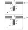
- FIG. 1illustrates a cross-sectional view of a step in a present process of fabricating a trench capacitor 130 , wherein a liner 114 is formed within a trench 106 .
- substrate 100may be processed as follows. First, a pad stack 102 may be formed on top of the substrate 100 .
- the pad stack 102may comprise one or more material layers.
- the pad stackincludes a pad oxide 102 a and a pad nitride 102 b that are deposited over the substrate 100 .
- a layer of borosilicate glass (BSG) or tetra-ethyl ortho silicate (TEOS)may be formed over the pad oxide 102 a and the pad nitride 102 b.
- BSGborosilicate glass
- TEOStetra-ethyl ortho silicate
- the trench 106is etched in the substrate 100 .
- the etchingmay be performed by, e.g., reactive ion etching (“RIE”) or an equivalent process, as is known in the art.
- RIEreactive ion etching
- the BSG layerif any, may be removed.
- Trench sidewalls 104extend through the pad stack 102 into the substrate 100 .
- the trench 106is preferably a high aspect ratio trench. As shown in FIG. 1, the trench 106 is a vertical trench having a tapered top. However, any suitable trench shape may be employed. By way of example only, the lower portion of the trench 106 may have a bottle shape, and the upper portion may or may not be tapered.
- a buried plate 112is preferably formed by implanting a dopant into the portion of the substrate 100 surrounding the sidewalls 104 in the lower portion of the trench.
- a node dielectric 110is then formed along the sidewalls 104 in the lower portion of the trench.
- the node dielectric 110may be selected from a variety of dielectric materials, although the node dielectric 110 preferably has a dielectric constant of at least 3.9, the dielectric constant of silicon dioxide.
- a collar 108is preferably formed along the sidewalls in the upper portion of the trench. The collar 108 may comprise an oxide.
- the liner 114is formed along the sidewalls 104 , preferably covering the node dielectric 110 and the collar 108 .
- the liner 114preferably comprises silicon or poly-Si, although other suitable fill materials may be used.
- the liner 114is preferably deposited using a CVD process. In one example, the CVD process is performed at a temperature between 560° C. to 650° C. and a pressure of between 10 to 50 mTorr. Most preferably, the temperature is 580° C. and the pressure is 15 mTorr.
- silane gasmay be flowed at a rate of 15-50 sccm. More preferably, the rate is 15 sccm. The growth rate is approximately 8 ⁇ per minute.
- the liner 114is preferably between 5-15 nm thick.
- an undesired native oxidemay be naturally formed over its surface when exposed to ambient air.
- the native oxidemay be removed using buffered hydrofluoric acid (BHF) or dilute hydrofluoric acid (DHF) as is known in the art.
- BHFbuffered hydrofluoric acid
- DHFdilute hydrofluoric acid
- An ozone treatmentmay be employed to remove any residues remaining on the sidewalls 104 .
- the ozone treatmentmay be performed prior to BHF or DHF etching.
- One example of an ozone treatmentemploys 10 ppm of ozone dissolved in DI water.
- an inner electrode 120 filleris then grown from the liner 114 .
- the inner electrode 120preferably comprises the same material as the liner 114 .
- the crystalline structure of the inner electrode 120may differ from that of the liner 114 .
- the inner electrode 120is grown using a rapid thermal CVD (“RTCVD”) process.
- RTCVDis a conventional CVD process performed at a high temperature to achieve rapid growth.
- the temperatureis preferably about 710° C.
- the pressureis about 15 mTorr
- silaneis flowed at about 400 sccm.
- the resultant growth rateis on the order of 27 ⁇ /second.
- the growth processpreferably occurs in a non-selective manner, meaning that the growth of poly-Si occurs wherever the liner 114 is located.
- the inner electrode 120is thus formed while substantially or entirely eliminating voids therein.
- a dopantmay be added during the growth process to in situ dope the inner electrode 120 .
- the inner electrode 120may be planarized and/or etched back or otherwise recessed within the trench 106 to a desired depth, e.g., to a point above or below the collar 108 . Then the fabrication process may continue in a conventional manner by, for example, forming an access transistor within the trench 106 over the trench capacitor 130 .
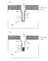
- FIG. 3illustrates a cross-sectional view of a substrate 200 at a step in a present process of fabricating a trench capacitor 230 .
- a trench 206may been formed within the substrate 200 by RIE or an equivalent process.
- the trenchhas sidewalls 204 which extend through a pad stack 202 into the substrate 200 .
- the pad stack 202may comprise a pad oxide 202 a and a pad nitride 202 b .
- the trench capacitor 230includes a buried plate 212 , a node dielectric 210 and a collar 208 .
- a liner 214 of, e.g., poly-Si or siliconis formed within the trench 206 .
- the liner 214is preferably formed as described above with regard to FIG. 1 .
- a second liner 216is preferably formed over the liner 214 by, e.g., deposition.
- the second liner 216is preferably a thin oxide layer on the order of 5 to 15 nm.
- the thin oxide layermay be formed, e.g., by CVD or a thermal process. Alternatively, a material such as a nitride formed by a thermal process may be employed.
- the second liner 216will be used as a mask in subsequent processing.
- FIG. 4illustrates a subsequent step after a portion of the second liner 216 has been removed.
- a layer of photoresist 218has been applied over the second liner 216 .
- the photoresist 218may be, e.g., a mid UV (“MUV”) resist, and is used as a mask, as is known in the art.
- the photoresistmay be planarized to provide a uniform surface.
- the photoresistis preferably recessed to a desired depth in the trench 206 , as shown in FIG. 4 . To ensure substantially void-free poly-Si fill, the desired depth is preferably recessed more than the recess depth for the poly-Si within the trench.
- any of the second liner 216 not covered by the photoresist 218is preferably entirely removed by, e.g., etching.
- the etching processis preferably a wet etch process. If the second liner 216 is an oxide, BHF is a preferred etchant. If the second liner 216 is a nitride, hot phosphoric acid is a preferred etchant.
- the photoresist 218is removed. Then portions of the liner 214 not covered by the second liner 216 are preferably removed by etching. This etching step is preferably performed isotropically, by, for example BHF. The result is shown in FIG. 5 .
- an inner electrode 220is grown from the liner 214 .
- a selective epitaxial silicon growth processis preferably used.
- the inner electrode 220may be doped in situ during formation. Because the inner electrode 220 is grown from the etched liner 214 , it is possible to eliminate the need to subsequently planarize the inner electrode 220 using, e.g., chemical mechanical planarization (“CMP”). It is also possible to eliminate recessing of the inner electrode 220 after its formation. Then the fabrication process may continue in a conventional manner.
- CMPchemical mechanical planarization
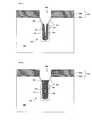
- FIG. 7illustrates a cross-sectional view of a step in a present process of healing a trench capacitor 330 having a void 318 therein.
- the trench 306has been formed.
- the trench 306has sidewalls 304 which extend through a pad stack 302 into the substrate 300 .
- the pad stack 302may comprise a pad oxide 302 a and a pad nitride 302 b .
- the trench capacitor 330includes a buried plate 312 , a node dielectric 310 and a collar 308 .
- the void 318 within an inner electrode 320has been exposed during, for example a poly-Si recess process.
- the inner electrode 320is preferably poly-Si.
- the collar 308is not materially affected by the processing of the present embodiment.
- epitaxial siliconis grown on the inner electrode 320 to substantially or completely fill the void/seam.
- the epitaxial siliconis preferably selectively grown by a two-step process.
- a UHV in situ desorption processis preferably performed at a temperature of about 750° C. and a pressure of about 4 ⁇ 10 ⁇ 8 Torr for approximately 15 minutes to remove any native oxide present on exposed surfaces.
- epitaxial siliconis selectively grown on silicon or poly-Si (but not oxide or nitride) at a temperature of about 650° C. and a pressure of about 120 mTorr.
- the silanemay be flowed, e.g., at a rate of 16 sccm and HCl may be flowed, e.g., at a rate of 12 sccm. This produces a growth rate on the order 5.8 ⁇ /min. As shown in FIG. 8, a small void 322 may remain in the healed inner electrode 320 .
- the epitaxial siliconmay be grown to fill the void and then form a substantially flat surface for the inner electrode 320 .
- the selective growthmay be continued to substantially or completely till the trench 306 .
- the inner electrode 320may be recessed to a desired depth by, e.g., etching. Because the void/seam is completely eliminated or minimized with the healing growth, the recessing preferably results in a substantially planar upper surface for the inner electrode 320 .
- further processingmay be performed on the trench capacitor 330 .
- substantially void-free fillersmay be formed within a semiconductor trench by first applying a liner along the sidewalls of the trench. These substantially void free fillers may be doped in situ. Another advantage of the present invention is that such fillers may be selectively grown to eliminate costly processing steps such as CMP and recessing. Yet another advantage of the present invention is that preexisting voids or other defects may be healed by selectively growing epitaxial silicon, thereby avoiding additional deposition steps as employed in prior solutions. A further advantage of the present invention is that capacitors can be fabricated without increased resistance due to voids formed therein.
Landscapes
- Engineering & Computer Science (AREA)
- Manufacturing & Machinery (AREA)
- Microelectronics & Electronic Packaging (AREA)
- General Physics & Mathematics (AREA)
- Condensed Matter Physics & Semiconductors (AREA)
- Computer Hardware Design (AREA)
- Physics & Mathematics (AREA)
- Power Engineering (AREA)
- Chemical & Material Sciences (AREA)
- Crystallography & Structural Chemistry (AREA)
- Materials Engineering (AREA)
- Semiconductor Memories (AREA)
- Semiconductor Integrated Circuits (AREA)
Abstract
Description
Claims (32)
Priority Applications (2)
| Application Number | Priority Date | Filing Date | Title |
|---|---|---|---|
| US10/386,880US6809005B2 (en) | 2003-03-12 | 2003-03-12 | Method to fill deep trench structures with void-free polysilicon or silicon |
| DE102004012241ADE102004012241A1 (en) | 2003-03-12 | 2004-03-12 | Process for filling deep trench structures with fillings without cavities |
Applications Claiming Priority (1)
| Application Number | Priority Date | Filing Date | Title |
|---|---|---|---|
| US10/386,880US6809005B2 (en) | 2003-03-12 | 2003-03-12 | Method to fill deep trench structures with void-free polysilicon or silicon |
Publications (2)
| Publication Number | Publication Date |
|---|---|
| US20040180510A1 US20040180510A1 (en) | 2004-09-16 |
| US6809005B2true US6809005B2 (en) | 2004-10-26 |
Family
ID=32961780
Family Applications (1)
| Application Number | Title | Priority Date | Filing Date |
|---|---|---|---|
| US10/386,880Expired - Fee RelatedUS6809005B2 (en) | 2003-03-12 | 2003-03-12 | Method to fill deep trench structures with void-free polysilicon or silicon |
Country Status (2)
| Country | Link |
|---|---|
| US (1) | US6809005B2 (en) |
| DE (1) | DE102004012241A1 (en) |
Cited By (33)
| Publication number | Priority date | Publication date | Assignee | Title |
|---|---|---|---|---|
| US20040188739A1 (en)* | 2003-01-08 | 2004-09-30 | Keiichi Takenaka | Semiconductor device including trench capacitor and manufacturing method of the same |
| US20080001196A1 (en)* | 2006-06-28 | 2008-01-03 | International Business Machines Corporation | Trench capacitors and memory cells using trench capacitors and method of fabricating same |
| US20080076230A1 (en)* | 2006-09-21 | 2008-03-27 | Kangguo Cheng | Trench Capacitor with Void-Free Conductor Fill |
| US7595524B2 (en) | 2003-05-20 | 2009-09-29 | Fairchild Semiconductor Corporation | Power device with trenches having wider upper portion than lower portion |
| US20090278237A1 (en)* | 2008-05-06 | 2009-11-12 | International Business Machines Corporation | Through substrate via including variable sidewall profile |
| US20100044785A1 (en)* | 2008-01-15 | 2010-02-25 | Murphy James J | High aspect ratio trench structures with void-free fill material |
| US20110177670A1 (en)* | 2010-01-20 | 2011-07-21 | International Business Machines Corporaton | Through silicon via lithographic alignment and registration |
| US20150137309A1 (en)* | 2006-03-01 | 2015-05-21 | Infineon Technologies Ag | Methods of Fabricating Isolation Regions of Semiconductor Devices and Structures Thereof |
| US9558931B2 (en) | 2012-07-27 | 2017-01-31 | Asm Ip Holding B.V. | System and method for gas-phase sulfur passivation of a semiconductor surface |
| US9589770B2 (en) | 2013-03-08 | 2017-03-07 | Asm Ip Holding B.V. | Method and systems for in-situ formation of intermediate reactive species |
| US9605343B2 (en) | 2013-11-13 | 2017-03-28 | Asm Ip Holding B.V. | Method for forming conformal carbon films, structures conformal carbon film, and system of forming same |
| US9605342B2 (en) | 2012-09-12 | 2017-03-28 | Asm Ip Holding B.V. | Process gas management for an inductively-coupled plasma deposition reactor |
| US9627221B1 (en) | 2015-12-28 | 2017-04-18 | Asm Ip Holding B.V. | Continuous process incorporating atomic layer etching |
| US9647114B2 (en) | 2015-08-14 | 2017-05-09 | Asm Ip Holding B.V. | Methods of forming highly p-type doped germanium tin films and structures and devices including the films |
| US9657845B2 (en) | 2014-10-07 | 2017-05-23 | Asm Ip Holding B.V. | Variable conductance gas distribution apparatus and method |
| US9659799B2 (en) | 2012-08-28 | 2017-05-23 | Asm Ip Holding B.V. | Systems and methods for dynamic semiconductor process scheduling |
| US9790595B2 (en) | 2013-07-12 | 2017-10-17 | Asm Ip Holding B.V. | Method and system to reduce outgassing in a reaction chamber |
| US9812526B2 (en) | 2015-10-19 | 2017-11-07 | Samsung Electronics Co., Ltd. | Three-dimensional semiconductor devices |
| US9837271B2 (en) | 2014-07-18 | 2017-12-05 | Asm Ip Holding B.V. | Process for forming silicon-filled openings with a reduced occurrence of voids |
| US9890456B2 (en) | 2014-08-21 | 2018-02-13 | Asm Ip Holding B.V. | Method and system for in situ formation of gas-phase compounds |
| US10083836B2 (en) | 2015-07-24 | 2018-09-25 | Asm Ip Holding B.V. | Formation of boron-doped titanium metal films with high work function |
| US10087525B2 (en) | 2015-08-04 | 2018-10-02 | Asm Ip Holding B.V. | Variable gap hard stop design |
| US10167557B2 (en) | 2014-03-18 | 2019-01-01 | Asm Ip Holding B.V. | Gas distribution system, reactor including the system, and methods of using the same |
| US10276355B2 (en) | 2015-03-12 | 2019-04-30 | Asm Ip Holding B.V. | Multi-zone reactor, system including the reactor, and method of using the same |
| US10458018B2 (en) | 2015-06-26 | 2019-10-29 | Asm Ip Holding B.V. | Structures including metal carbide material, devices including the structures, and methods of forming same |
| US10460932B2 (en) | 2017-03-31 | 2019-10-29 | Asm Ip Holding B.V. | Semiconductor device with amorphous silicon filled gaps and methods for forming |
| US10529542B2 (en) | 2015-03-11 | 2020-01-07 | Asm Ip Holdings B.V. | Cross-flow reactor and method |
| US10600673B2 (en) | 2015-07-07 | 2020-03-24 | Asm Ip Holding B.V. | Magnetic susceptor to baseplate seal |
| US10804098B2 (en) | 2009-08-14 | 2020-10-13 | Asm Ip Holding B.V. | Systems and methods for thin-film deposition of metal oxides using excited nitrogen-oxygen species |
| US10858737B2 (en) | 2014-07-28 | 2020-12-08 | Asm Ip Holding B.V. | Showerhead assembly and components thereof |
| US10941490B2 (en) | 2014-10-07 | 2021-03-09 | Asm Ip Holding B.V. | Multiple temperature range susceptor, assembly, reactor and system including the susceptor, and methods of using the same |
| US11015245B2 (en) | 2014-03-19 | 2021-05-25 | Asm Ip Holding B.V. | Gas-phase reactor and system having exhaust plenum and components thereof |
| US20230282688A1 (en)* | 2022-01-28 | 2023-09-07 | Semiconductor Components Industries, Llc | Electronic device including a semiconductor layer within a trench and a semiconductor layer and a process of forming the same |
Families Citing this family (25)
| Publication number | Priority date | Publication date | Assignee | Title |
|---|---|---|---|---|
| US7154159B2 (en)* | 2004-02-24 | 2006-12-26 | Nanya Technology Corporation | Trench isolation structure and method of forming the same |
| US8120140B2 (en)* | 2009-05-22 | 2012-02-21 | Macronix International Co., Ltd. | Isolation structure and formation method thereof |
| JP6056292B2 (en) | 2012-09-12 | 2017-01-11 | 住友電気工業株式会社 | Method for manufacturing silicon carbide semiconductor device |
| JP2014056913A (en) | 2012-09-12 | 2014-03-27 | Sumitomo Electric Ind Ltd | Silicon carbide semiconductor device |
| JP5811973B2 (en) | 2012-09-12 | 2015-11-11 | 住友電気工業株式会社 | Method for manufacturing silicon carbide semiconductor device |
| US9343294B2 (en)* | 2014-04-28 | 2016-05-17 | Taiwan Semiconductor Manufacturing Company, Ltd. | Interconnect structure having air gap and method of forming the same |
| US10049927B2 (en)* | 2016-06-10 | 2018-08-14 | Applied Materials, Inc. | Seam-healing method upon supra-atmospheric process in diffusion promoting ambient |
| US10224224B2 (en) | 2017-03-10 | 2019-03-05 | Micromaterials, LLC | High pressure wafer processing systems and related methods |
| US10622214B2 (en) | 2017-05-25 | 2020-04-14 | Applied Materials, Inc. | Tungsten defluorination by high pressure treatment |
| US10461152B2 (en) | 2017-07-10 | 2019-10-29 | Globalfoundries Inc. | Radio frequency switches with air gap structures |
| WO2019036157A1 (en) | 2017-08-18 | 2019-02-21 | Applied Materials, Inc. | High pressure and high temperature anneal chamber |
| US10276411B2 (en) | 2017-08-18 | 2019-04-30 | Applied Materials, Inc. | High pressure and high temperature anneal chamber |
| US10833153B2 (en) | 2017-09-13 | 2020-11-10 | Globalfoundries Inc. | Switch with local silicon on insulator (SOI) and deep trench isolation |
| CN117936420A (en) | 2017-11-11 | 2024-04-26 | 微材料有限责任公司 | Gas delivery system for high pressure processing chamber |
| KR20200075892A (en) | 2017-11-17 | 2020-06-26 | 어플라이드 머티어리얼스, 인코포레이티드 | Condenser system for high pressure treatment systems |
| US10446643B2 (en)* | 2018-01-22 | 2019-10-15 | Globalfoundries Inc. | Sealed cavity structures with a planar surface |
| SG11202008256WA (en) | 2018-03-09 | 2020-09-29 | Applied Materials Inc | High pressure annealing process for metal containing materials |
| US10950429B2 (en) | 2018-05-08 | 2021-03-16 | Applied Materials, Inc. | Methods of forming amorphous carbon hard mask layers and hard mask layers formed therefrom |
| US10748783B2 (en) | 2018-07-25 | 2020-08-18 | Applied Materials, Inc. | Gas delivery module |
| US11410872B2 (en) | 2018-11-30 | 2022-08-09 | Globalfoundries U.S. Inc. | Oxidized cavity structures within and under semiconductor devices |
| WO2020117462A1 (en) | 2018-12-07 | 2020-06-11 | Applied Materials, Inc. | Semiconductor processing system |
| US10923577B2 (en) | 2019-01-07 | 2021-02-16 | Globalfoundries U.S. Inc. | Cavity structures under shallow trench isolation regions |
| US11127816B2 (en) | 2020-02-14 | 2021-09-21 | Globalfoundries U.S. Inc. | Heterojunction bipolar transistors with one or more sealed airgap |
| US11901222B2 (en) | 2020-02-17 | 2024-02-13 | Applied Materials, Inc. | Multi-step process for flowable gap-fill film |
| US12213305B2 (en)* | 2021-04-15 | 2025-01-28 | Changxin Memory Technologies, Inc. | Manufacturing method of semiconductor structure with epitaxial layer forming extension portion |
Citations (5)
| Publication number | Priority date | Publication date | Assignee | Title |
|---|---|---|---|---|
| US5234856A (en)* | 1992-04-15 | 1993-08-10 | Micron Technology, Inc. | Dynamic random access memory cell having a stacked-trench capacitor that is resistant to alpha particle generated soft errors, and method of manufacturing same |
| US6083828A (en)* | 1999-01-27 | 2000-07-04 | United Integrated Circuits Corp. | Method for forming a self-aligned contact |
| US20010001175A1 (en) | 1998-04-21 | 2001-05-17 | Pravin Narwankar | Method and apparatus for modifying the profile of narrow, high-aspect-ratio gaps using differential plasma power |
| US20010021592A1 (en) | 2000-03-08 | 2001-09-13 | Jusung Engineering Co., Ltd. | High density plasma chemical vapor deposition apparatus and gap filling method using the same |
| US6677197B2 (en)* | 2001-12-31 | 2004-01-13 | Infineon Technologies Ag | High aspect ratio PBL SiN barrier formation |
- 2003
- 2003-03-12USUS10/386,880patent/US6809005B2/ennot_activeExpired - Fee Related
- 2004
- 2004-03-12DEDE102004012241Apatent/DE102004012241A1/ennot_activeCeased
Patent Citations (5)
| Publication number | Priority date | Publication date | Assignee | Title |
|---|---|---|---|---|
| US5234856A (en)* | 1992-04-15 | 1993-08-10 | Micron Technology, Inc. | Dynamic random access memory cell having a stacked-trench capacitor that is resistant to alpha particle generated soft errors, and method of manufacturing same |
| US20010001175A1 (en) | 1998-04-21 | 2001-05-17 | Pravin Narwankar | Method and apparatus for modifying the profile of narrow, high-aspect-ratio gaps using differential plasma power |
| US6083828A (en)* | 1999-01-27 | 2000-07-04 | United Integrated Circuits Corp. | Method for forming a self-aligned contact |
| US20010021592A1 (en) | 2000-03-08 | 2001-09-13 | Jusung Engineering Co., Ltd. | High density plasma chemical vapor deposition apparatus and gap filling method using the same |
| US6677197B2 (en)* | 2001-12-31 | 2004-01-13 | Infineon Technologies Ag | High aspect ratio PBL SiN barrier formation |
Cited By (51)
| Publication number | Priority date | Publication date | Assignee | Title |
|---|---|---|---|---|
| US20040188739A1 (en)* | 2003-01-08 | 2004-09-30 | Keiichi Takenaka | Semiconductor device including trench capacitor and manufacturing method of the same |
| US8716783B2 (en) | 2003-05-20 | 2014-05-06 | Fairchild Semiconductor Corporation | Power device with self-aligned source regions |
| US8034682B2 (en) | 2003-05-20 | 2011-10-11 | Fairchild Semiconductor Corporation | Power device with trenches having wider upper portion than lower portion |
| US7595524B2 (en) | 2003-05-20 | 2009-09-29 | Fairchild Semiconductor Corporation | Power device with trenches having wider upper portion than lower portion |
| US7799636B2 (en) | 2003-05-20 | 2010-09-21 | Fairchild Semiconductor Corporation | Power device with trenches having wider upper portion than lower portion |
| US20150137309A1 (en)* | 2006-03-01 | 2015-05-21 | Infineon Technologies Ag | Methods of Fabricating Isolation Regions of Semiconductor Devices and Structures Thereof |
| US9653543B2 (en)* | 2006-03-01 | 2017-05-16 | Infineon Technologies Ag | Methods of fabricating isolation regions of semiconductor devices and structures thereof |
| US20080001196A1 (en)* | 2006-06-28 | 2008-01-03 | International Business Machines Corporation | Trench capacitors and memory cells using trench capacitors and method of fabricating same |
| US20080246068A1 (en)* | 2006-06-28 | 2008-10-09 | Kangguo Cheng | Trench capacitors and memory cells using trench capacitors |
| US7888722B2 (en)* | 2006-06-28 | 2011-02-15 | International Business Machines Corporation | Trench capacitors and memory cells using trench capacitors |
| US7709320B2 (en)* | 2006-06-28 | 2010-05-04 | International Business Machines Corporation | Method of fabricating trench capacitors and memory cells using trench capacitors |
| US7494891B2 (en)* | 2006-09-21 | 2009-02-24 | International Business Machines Corporation | Trench capacitor with void-free conductor fill |
| US20080076230A1 (en)* | 2006-09-21 | 2008-03-27 | Kangguo Cheng | Trench Capacitor with Void-Free Conductor Fill |
| US20100044785A1 (en)* | 2008-01-15 | 2010-02-25 | Murphy James J | High aspect ratio trench structures with void-free fill material |
| US7956411B2 (en) | 2008-01-15 | 2011-06-07 | Fairchild Semiconductor Corporation | High aspect ratio trench structures with void-free fill material |
| US8198196B1 (en) | 2008-01-15 | 2012-06-12 | Fairchild Semiconductor Corporation | High aspect ratio trench structures with void-free fill material |
| US20090278237A1 (en)* | 2008-05-06 | 2009-11-12 | International Business Machines Corporation | Through substrate via including variable sidewall profile |
| US8643190B2 (en) | 2008-05-06 | 2014-02-04 | Ultratech, Inc. | Through substrate via including variable sidewall profile |
| US20110068477A1 (en)* | 2008-05-06 | 2011-03-24 | International Business Machines Corporation | Through substrate via including variable sidewall profile |
| US7863180B2 (en) | 2008-05-06 | 2011-01-04 | International Business Machines Corporation | Through substrate via including variable sidewall profile |
| WO2009137313A1 (en)* | 2008-05-06 | 2009-11-12 | International Business Machines Corporation | Through substrate via including variable sidewall profile |
| US10804098B2 (en) | 2009-08-14 | 2020-10-13 | Asm Ip Holding B.V. | Systems and methods for thin-film deposition of metal oxides using excited nitrogen-oxygen species |
| WO2011090852A2 (en) | 2010-01-20 | 2011-07-28 | International Business Machines Corporation | Through silicon via lithographic alignment and registration |
| US8039356B2 (en) | 2010-01-20 | 2011-10-18 | International Business Machines Corporation | Through silicon via lithographic alignment and registration |
| US20110177670A1 (en)* | 2010-01-20 | 2011-07-21 | International Business Machines Corporaton | Through silicon via lithographic alignment and registration |
| DE112011100134T5 (en) | 2010-01-20 | 2012-10-04 | International Business Machines Corporation | Continuous silicon connection with lithographic alignment and registration |
| US9558931B2 (en) | 2012-07-27 | 2017-01-31 | Asm Ip Holding B.V. | System and method for gas-phase sulfur passivation of a semiconductor surface |
| US9659799B2 (en) | 2012-08-28 | 2017-05-23 | Asm Ip Holding B.V. | Systems and methods for dynamic semiconductor process scheduling |
| US9605342B2 (en) | 2012-09-12 | 2017-03-28 | Asm Ip Holding B.V. | Process gas management for an inductively-coupled plasma deposition reactor |
| US9589770B2 (en) | 2013-03-08 | 2017-03-07 | Asm Ip Holding B.V. | Method and systems for in-situ formation of intermediate reactive species |
| US9790595B2 (en) | 2013-07-12 | 2017-10-17 | Asm Ip Holding B.V. | Method and system to reduce outgassing in a reaction chamber |
| US9605343B2 (en) | 2013-11-13 | 2017-03-28 | Asm Ip Holding B.V. | Method for forming conformal carbon films, structures conformal carbon film, and system of forming same |
| US10167557B2 (en) | 2014-03-18 | 2019-01-01 | Asm Ip Holding B.V. | Gas distribution system, reactor including the system, and methods of using the same |
| US11015245B2 (en) | 2014-03-19 | 2021-05-25 | Asm Ip Holding B.V. | Gas-phase reactor and system having exhaust plenum and components thereof |
| US9837271B2 (en) | 2014-07-18 | 2017-12-05 | Asm Ip Holding B.V. | Process for forming silicon-filled openings with a reduced occurrence of voids |
| US10858737B2 (en) | 2014-07-28 | 2020-12-08 | Asm Ip Holding B.V. | Showerhead assembly and components thereof |
| US9890456B2 (en) | 2014-08-21 | 2018-02-13 | Asm Ip Holding B.V. | Method and system for in situ formation of gas-phase compounds |
| US10941490B2 (en) | 2014-10-07 | 2021-03-09 | Asm Ip Holding B.V. | Multiple temperature range susceptor, assembly, reactor and system including the susceptor, and methods of using the same |
| US9657845B2 (en) | 2014-10-07 | 2017-05-23 | Asm Ip Holding B.V. | Variable conductance gas distribution apparatus and method |
| US10529542B2 (en) | 2015-03-11 | 2020-01-07 | Asm Ip Holdings B.V. | Cross-flow reactor and method |
| US10276355B2 (en) | 2015-03-12 | 2019-04-30 | Asm Ip Holding B.V. | Multi-zone reactor, system including the reactor, and method of using the same |
| US10458018B2 (en) | 2015-06-26 | 2019-10-29 | Asm Ip Holding B.V. | Structures including metal carbide material, devices including the structures, and methods of forming same |
| US10600673B2 (en) | 2015-07-07 | 2020-03-24 | Asm Ip Holding B.V. | Magnetic susceptor to baseplate seal |
| US10083836B2 (en) | 2015-07-24 | 2018-09-25 | Asm Ip Holding B.V. | Formation of boron-doped titanium metal films with high work function |
| US10087525B2 (en) | 2015-08-04 | 2018-10-02 | Asm Ip Holding B.V. | Variable gap hard stop design |
| US9647114B2 (en) | 2015-08-14 | 2017-05-09 | Asm Ip Holding B.V. | Methods of forming highly p-type doped germanium tin films and structures and devices including the films |
| US9812526B2 (en) | 2015-10-19 | 2017-11-07 | Samsung Electronics Co., Ltd. | Three-dimensional semiconductor devices |
| US9627221B1 (en) | 2015-12-28 | 2017-04-18 | Asm Ip Holding B.V. | Continuous process incorporating atomic layer etching |
| US10460932B2 (en) | 2017-03-31 | 2019-10-29 | Asm Ip Holding B.V. | Semiconductor device with amorphous silicon filled gaps and methods for forming |
| US20230282688A1 (en)* | 2022-01-28 | 2023-09-07 | Semiconductor Components Industries, Llc | Electronic device including a semiconductor layer within a trench and a semiconductor layer and a process of forming the same |
| US12166068B2 (en)* | 2022-01-28 | 2024-12-10 | Semiconductor Components Industries, Llc | Electronic device including a semiconductor layer within a trench and a semiconductor layer and a process of forming the same |
Also Published As
| Publication number | Publication date |
|---|---|
| US20040180510A1 (en) | 2004-09-16 |
| DE102004012241A1 (en) | 2004-10-28 |
Similar Documents
| Publication | Publication Date | Title |
|---|---|---|
| US6809005B2 (en) | Method to fill deep trench structures with void-free polysilicon or silicon | |
| US7157327B2 (en) | Void free, silicon filled trenches in semiconductors | |
| KR100532509B1 (en) | Trench capacitor using SiGe layer and method of fabricating the same | |
| US6780728B2 (en) | Semiconductor constructions, and methods of forming semiconductor constructions | |
| US6967132B2 (en) | Methods of forming semiconductor circuitry | |
| US7893480B2 (en) | Trench memory with self-aligned strap formed by self-limiting process | |
| US20070141771A1 (en) | Integrated circuits and methods of forming a field effect transistor | |
| JP2000124303A (en) | Manufacturing method of trench isolation | |
| CN1832183A (en) | Structures and methods for providing buried plates for trench capacitor arrays | |
| US6472262B2 (en) | Method for fabricating a bipolar transistor of the self-aligned double-polysilicon type with a heterojunction base and corresponding transistor | |
| US7199414B2 (en) | Stress-reduced layer system for use in storage capacitors | |
| US6846744B1 (en) | Method of fabricating a bottle shaped deep trench for trench capacitor DRAM devices | |
| US20030005881A1 (en) | Method for forming contact plug of semiconductor device | |
| KR100517328B1 (en) | Semiconductor device having contact plug using selective epitaxial growth and method of fabricating the same | |
| US6103568A (en) | Manufacturing method of cylindrical stacked electrode | |
| US20070022941A1 (en) | Method of forming a layer and method of manufacturing a semiconductor device using the same | |
| US20050277247A1 (en) | Method for fabricating a trench capacitor of dram | |
| US6506657B1 (en) | Process for forming damascene-type isolation structure for BJT device formed in trench | |
| JP4197576B2 (en) | Manufacturing method of semiconductor device | |
| KR20030002745A (en) | Method of manufacturing a semiconductor device | |
| US7094658B2 (en) | 3-stage method for forming deep trench structure and deep trench capacitor | |
| US6245633B1 (en) | Fabrication method for a double-side double-crown stacked capacitor | |
| US6825094B2 (en) | Method for increasing capacitance of deep trench capacitors | |
| US5753552A (en) | Method for fabricating a storage electrode without polysilicon bridge and undercut | |
| KR20000075235A (en) | Method for forming device isolation |
Legal Events
| Date | Code | Title | Description |
|---|---|---|---|
| AS | Assignment | Owner name:INTERNATIONAL BUSINESS MACHINES CORPORATION, NEW Y Free format text:ASSIGNMENT OF ASSIGNORS INTEREST;ASSIGNORS:CHAN, KEVIN K.;KULKARNI, SUBHASH B.;REEL/FRAME:014120/0986;SIGNING DATES FROM 20030411 TO 20030416 Owner name:INFINEON TECHNOLOGIES NORTH AMERICA CORP., CALIFOR Free format text:ASSIGNMENT OF ASSIGNORS INTEREST;ASSIGNORS:RANADE, RAJIV;MATHAD, GANGADHARA S.;REEL/FRAME:014120/0494;SIGNING DATES FROM 20030412 TO 20030414 | |
| AS | Assignment | Owner name:INFINEON TECHNOLOGIES AG, GERMANY Free format text:ASSIGNMENT OF ASSIGNORS INTEREST;ASSIGNOR:INFINEON TECHNOLOGIES NORTH AMERICA CORP.;REEL/FRAME:014253/0557 Effective date:20040113 | |
| FPAY | Fee payment | Year of fee payment:4 | |
| AS | Assignment | Owner name:QIMONDA AG, GERMANY Free format text:ASSIGNMENT OF ASSIGNORS INTEREST;ASSIGNOR:INFINEON TECHNOLOGIES AG;REEL/FRAME:023788/0535 Effective date:20060425 | |
| FPAY | Fee payment | Year of fee payment:8 | |
| AS | Assignment | Owner name:INFINEON TECHNOLOGIES AG, GERMANY Free format text:ASSIGNMENT OF ASSIGNORS INTEREST;ASSIGNOR:QIMONDA AG;REEL/FRAME:035623/0001 Effective date:20141009 | |
| REMI | Maintenance fee reminder mailed | ||
| LAPS | Lapse for failure to pay maintenance fees | ||
| STCH | Information on status: patent discontinuation | Free format text:PATENT EXPIRED DUE TO NONPAYMENT OF MAINTENANCE FEES UNDER 37 CFR 1.362 | |
| FP | Lapsed due to failure to pay maintenance fee | Effective date:20161026 |