US6807079B2 - Device having a state dependent upon the state of particles dispersed in a carrier - Google Patents
Device having a state dependent upon the state of particles dispersed in a carrierDownload PDFInfo
- Publication number
- US6807079B2 US6807079B2US10/285,802US28580202AUS6807079B2US 6807079 B2US6807079 B2US 6807079B2US 28580202 AUS28580202 AUS 28580202AUS 6807079 B2US6807079 B2US 6807079B2
- Authority
- US
- United States
- Prior art keywords
- particles
- set forth
- layer
- electrodes
- memory cell
- Prior art date
- Legal status (The legal status is an assumption and is not a legal conclusion. Google has not performed a legal analysis and makes no representation as to the accuracy of the status listed.)
- Expired - Fee Related
Links
Images

Classifications
- G—PHYSICS
- G11—INFORMATION STORAGE
- G11C—STATIC STORES
- G11C16/00—Erasable programmable read-only memories
- G11C16/02—Erasable programmable read-only memories electrically programmable
- G—PHYSICS
- G11—INFORMATION STORAGE
- G11C—STATIC STORES
- G11C17/00—Read-only memories programmable only once; Semi-permanent stores, e.g. manually-replaceable information cards
- G11C17/14—Read-only memories programmable only once; Semi-permanent stores, e.g. manually-replaceable information cards in which contents are determined by selectively establishing, breaking or modifying connecting links by permanently altering the state of coupling elements, e.g. PROM
- G11C17/16—Read-only memories programmable only once; Semi-permanent stores, e.g. manually-replaceable information cards in which contents are determined by selectively establishing, breaking or modifying connecting links by permanently altering the state of coupling elements, e.g. PROM using electrically-fusible links
- H—ELECTRICITY
- H01—ELECTRIC ELEMENTS
- H01L—SEMICONDUCTOR DEVICES NOT COVERED BY CLASS H10
- H01L23/00—Details of semiconductor or other solid state devices
- H01L23/52—Arrangements for conducting electric current within the device in operation from one component to another, i.e. interconnections, e.g. wires, lead frames
- H01L23/522—Arrangements for conducting electric current within the device in operation from one component to another, i.e. interconnections, e.g. wires, lead frames including external interconnections consisting of a multilayer structure of conductive and insulating layers inseparably formed on the semiconductor body
- H01L23/525—Arrangements for conducting electric current within the device in operation from one component to another, i.e. interconnections, e.g. wires, lead frames including external interconnections consisting of a multilayer structure of conductive and insulating layers inseparably formed on the semiconductor body with adaptable interconnections
- H01L23/5252—Arrangements for conducting electric current within the device in operation from one component to another, i.e. interconnections, e.g. wires, lead frames including external interconnections consisting of a multilayer structure of conductive and insulating layers inseparably formed on the semiconductor body with adaptable interconnections comprising anti-fuses, i.e. connections having their state changed from non-conductive to conductive
- H—ELECTRICITY
- H01—ELECTRIC ELEMENTS
- H01L—SEMICONDUCTOR DEVICES NOT COVERED BY CLASS H10
- H01L23/00—Details of semiconductor or other solid state devices
- H01L23/52—Arrangements for conducting electric current within the device in operation from one component to another, i.e. interconnections, e.g. wires, lead frames
- H01L23/522—Arrangements for conducting electric current within the device in operation from one component to another, i.e. interconnections, e.g. wires, lead frames including external interconnections consisting of a multilayer structure of conductive and insulating layers inseparably formed on the semiconductor body
- H01L23/525—Arrangements for conducting electric current within the device in operation from one component to another, i.e. interconnections, e.g. wires, lead frames including external interconnections consisting of a multilayer structure of conductive and insulating layers inseparably formed on the semiconductor body with adaptable interconnections
- H01L23/5256—Arrangements for conducting electric current within the device in operation from one component to another, i.e. interconnections, e.g. wires, lead frames including external interconnections consisting of a multilayer structure of conductive and insulating layers inseparably formed on the semiconductor body with adaptable interconnections comprising fuses, i.e. connections having their state changed from conductive to non-conductive
- H—ELECTRICITY
- H10—SEMICONDUCTOR DEVICES; ELECTRIC SOLID-STATE DEVICES NOT OTHERWISE PROVIDED FOR
- H10B—ELECTRONIC MEMORY DEVICES
- H10B63/00—Resistance change memory devices, e.g. resistive RAM [ReRAM] devices
- H10B63/80—Arrangements comprising multiple bistable or multi-stable switching components of the same type on a plane parallel to the substrate, e.g. cross-point arrays
- H—ELECTRICITY
- H10—SEMICONDUCTOR DEVICES; ELECTRIC SOLID-STATE DEVICES NOT OTHERWISE PROVIDED FOR
- H10N—ELECTRIC SOLID-STATE DEVICES NOT OTHERWISE PROVIDED FOR
- H10N70/00—Solid-state devices having no potential barriers, and specially adapted for rectifying, amplifying, oscillating or switching
- H10N70/20—Multistable switching devices, e.g. memristors
- H10N70/24—Multistable switching devices, e.g. memristors based on migration or redistribution of ionic species, e.g. anions, vacancies
- H10N70/245—Multistable switching devices, e.g. memristors based on migration or redistribution of ionic species, e.g. anions, vacancies the species being metal cations, e.g. programmable metallization cells
- H—ELECTRICITY
- H10—SEMICONDUCTOR DEVICES; ELECTRIC SOLID-STATE DEVICES NOT OTHERWISE PROVIDED FOR
- H10N—ELECTRIC SOLID-STATE DEVICES NOT OTHERWISE PROVIDED FOR
- H10N70/00—Solid-state devices having no potential barriers, and specially adapted for rectifying, amplifying, oscillating or switching
- H10N70/801—Constructional details of multistable switching devices
- H10N70/821—Device geometry
- H10N70/826—Device geometry adapted for essentially vertical current flow, e.g. sandwich or pillar type devices
- H—ELECTRICITY
- H10—SEMICONDUCTOR DEVICES; ELECTRIC SOLID-STATE DEVICES NOT OTHERWISE PROVIDED FOR
- H10N—ELECTRIC SOLID-STATE DEVICES NOT OTHERWISE PROVIDED FOR
- H10N70/00—Solid-state devices having no potential barriers, and specially adapted for rectifying, amplifying, oscillating or switching
- H10N70/801—Constructional details of multistable switching devices
- H10N70/881—Switching materials
- H—ELECTRICITY
- H01—ELECTRIC ELEMENTS
- H01L—SEMICONDUCTOR DEVICES NOT COVERED BY CLASS H10
- H01L2924/00—Indexing scheme for arrangements or methods for connecting or disconnecting semiconductor or solid-state bodies as covered by H01L24/00
- H01L2924/0001—Technical content checked by a classifier
- H01L2924/0002—Not covered by any one of groups H01L24/00, H01L24/00 and H01L2224/00
Definitions
- Fuse and anti-fuse switchestypically include a thin film disposed between first and second electrodes. Such switches have been employed, for example, in memory devices, wherein a selected phase or memory state, such as “1” or “0”, is created by selectively applying current or voltage across the first and second electrodes in order to vary the conductance between the first and second electrodes. Such memory devices are typically, but not necessarily, one-time programmable or write-once memory devices. Alternatively, such memory devices can be erasable or phase-reversible to facilitate numerous read/write cycles.
- a switch known as a Le Comber switchutilizes diffusive metals, such as gold (Ag), for one of the two electrodes.
- diffusive metalssuch as gold may not be the most desirable material for the conduction lines.
- One solution to this problemis to employ multi-layer metal films for conduction lines and memory cells. However, this solution requires additional processing steps that increase the cost of device fabrication.
- the thin film materialhas anisotropic electrical properties, which requires costly photolithographic processing and limits the achievable density.
- the thin film materialis required to exhibit low electrical resistance between the first and second electrodes, before switching (i.e., when in the “on” state), while exhibiting high electrical resistance between neighboring switches, and is also required to exhibit high electrical resistance between the first and second electrodes, after switching (i.e., when in the “off” state).
- Anti-fuse switchesrequire similar anisotropic electrical properties.
- the present inventionencompasses, among other things, a device that includes a layer of material having particles dispersed therein, a first electrode on a first surface of the layer, and a second electrode on a second surface of the layer opposite the first surface. A state of the particles is changed when a prescribed voltage is applied across the first and second electrodes.
- the present inventionadditionally encompasses various embodiments of switches and memory cells, and devices incorporating the same.
- FIGS. 1A-1Dare partial, cross-sectional views of a device according to an embodiment of the present invention.
- FIGS. 2A-2Bare partial, cross-sectional views of a device according to another embodiment of the present invention.
- FIGS. 3A-3Bare partial, cross-sectional views of a device according to another embodiment of the present invention.
- FIG. 4is a perspective, cross-sectional view of a device according to another embodiment of the present invention.
- microparticlesrefers to particles having a maximum dimension that is much smaller than the thickness of the carrier in which the particles are dispersed, for example, 1 ⁇ 3 to ⁇ fraction (1/20) ⁇ of the thickness of the carrier.
- the size of the microparticles used in the practice of the present inventionis scalable in accordance with the geometry of the host device, and is not limiting to the present invention.
- nanoparticlesrefers to particles having a maximum dimension in the range of a nanometer to a micrometer.
- the particlesare either spherical or rod-shaped. However, neither the size nor shape of the particles are limiting to the present invention, in its broadest sense.
- carrierrefers to an electrically resistive material within which the particles are dispersed.
- the carrier materialmay suitably be composed of polyamide, polyester, UV-curable polymer, or spin-on glass, or any suitable combination of these or other electrically resistive materials, such as electrically-resistive organic or inorganic materials.
- the carrier materialis a thin, flexible, resilient, or viscoelastic material, such as a gel or gel-like material.
- the carrier materialcan be a liquid or viscous material sandwiched between, or encapsulated by, other material layers, for example, in a manner such as the liquid crystal material in a liquid crystal display (LCD) panel.
- LCDliquid crystal display
- switchrefers to a device which has at least two different phases or states, wherein the state of the device can be programmed at least once.
- switchas used herein broadly encompasses both one-time programmable (write-once) devices, as well as erasable or phase-reversible (write-many) devices whose phase or state can be switched or re-programmed multiple times. The number of times that the phase or state of the switch can be re-programmed or switched is not limiting to the present invention.
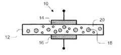
- the anti-fuse switch 10constructed in accordance with a first embodiment of the present invention.
- the anti-fuse switch 10includes a layer or thin film 12 disposed between a first electrode 14 and a second electrode 16 .
- the layer 12is formed by particles 18 dispersed in a carrier 20 .
- the particles 18 of this embodimentare preferably microparticles or nanoparticles that may suitably be composed of a diffusive metal, such as silver, palladium-silver alloy, copper, aluminum, carbon, carbon-silver blend, or gold, or any other suitable organic, inorganic, or ferroelectric material that is electrically conductive, or any combination thereof.
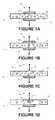
- the anti-fuse switch 10 depicted in FIGS. 1A-1Dworks in the following manner.
- the particles 18are dispersed and do not form a conductive path between the first and second electrodes 14 , 16 .
- a prescribed voltage(“turn-on voltage”), e.g., a high voltage, is applied across the first and second electrodes 14 , 16 , the particles 18 diffuse and reorient due to the electrostatic forces on the particles from the electrodes.
- the diffusion of the particles 18causes an agglomeration or concentration (increased density) of particles 18 in an electrode region of the carrier 20 between the first and second electrodes 14 , 16 , and a depletion (decreased density) of the particles 18 in peripheral regions of the carrier 20 outside of the electrode region.
- the thickness of the carrier 20 and the dispersion density of the particles 18 in the carrier 20are preferably selected so that the probability of obtaining at least one conductive path between the first and second electrodes 14 , 16 is close to 100%.
- percolation thresholdrefers to a thickness of the carrier 20 at which the probability of obtaining at least one conductive path between the first and second electrodes 14 , 16 is close to 100% for a given voltage applied across the first and second electrodes 14 , 16 . This probability depends exponentially on the thickness of the carrier material and on the volume fraction of the carrier material occupied by the particles 18 .
- the migration of the particles 18 that occurs in response to the application of the turn-on voltageresults in the formation of a conductive path between the first and second electrodes 14 , 16 , by way of the particles 18 agglomerating or fusing together to form a wire or fuse 22 between the first and second electrodes 14 , 16 , as is depicted in FIGS. 1B and 1D.
- the switch 10when a turn-on voltage is applied across the first and second electrodes 14 and 16 , the switch 10 is turned on; when a turn-on voltage is not applied across the first and second electrodes 14 and 16 , the switch 10 is turned off.
- the speed and reliability of the switch 10can be enhanced by application of a turn-on voltage in the form of a large electric field gradient G having sharp field tips, as is depicted in FIGS. 1C-1D.
- the field gradient Gexerts lateral forces on the particles 18 that induce movement of the particles 18 towards the center of the electrode region 17 of the carrier 20 , as is depicted in FIG. 1 D.
- the field gradient Gcan be created in any suitable manner, such as, for example, by using an appropriately-shaped electrode or Spindt emitter 21 .
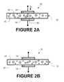
- the fuse switch 30includes a layer or thin film 32 disposed between a first electrode 34 and a second electrode 36 .
- the layer 32is formed by particles 38 dispersed in a carrier 40 .
- the particles 38 of this embodimentare preferably microparticles or nanoparticles that may suitably be composed of an oxidizing metal, such as titanium, iron, copper, aluminum, or any other suitable organic or inorganic material that is electrically conductive, or any combination thereof.
- the fuse switch 30 depicted in FIGS. 2A-2Bworks in the following manner.
- the particles 38are agglomerated or fused together to form a conductive path or fuse 42 between the first and second electrodes 34 , 36 , in the same manner as when the anti-fuse switch 10 is in its “on” state.
- Thiscan be accomplished, for example, by programming the switch 30 during or subsequent to manufacturing.
- FIG. 2AAs is depicted in FIG. 2A, when the fuse switch 30 is in its initial state, the particles 38 are agglomerated or fused together to form a conductive path or fuse 42 between the first and second electrodes 34 , 36 , in the same manner as when the anti-fuse switch 10 is in its “on” state. This can be accomplished, for example, by programming the switch 30 during or subsequent to manufacturing. As is depicted in FIG.
- a prescribed voltagee.g., a high voltage
- a currentflows through the conductive path or fuse 42 that causes the agglomerated particles 38 to dissociate or disintegrate, in a manner similar to how an automotive fuse is blown.
- the fuse switch 30is switched to its “off” state.
- the carrier material of this embodimentmay contain a suitable oxidant, such as air, hydrogen peroxide or a solid state oxidant such as CrO 2 F 2 , CrOF 3 , CrOF 2 , M 2 CrO 2 F 4 , M 2 CrO 2 (CF 3 COO) 4 , peroxo-bridged iron porphyrin dimers, ferryl (Fe IV O 2+ ) porphyrins and complexes of alkyl peroxides, so that when current flows through the conductive path 42 , an oxidation reaction between the oxidant and particle materials (e.g., copper) is triggered that oxidizes the particles 38 , thereby electrically isolating the particles 38 and breaking the conductive path 42 .
- a suitable oxidantsuch as air, hydrogen peroxide or a solid state oxidant such as CrO 2 F 2 , CrOF 3 , CrOF 2 , M 2 CrO 2 F 4 , M 2 CrO 2 (CF 3 COO) 4 , pe
- the anti-fuse switch 10 and the fuse switch 30have opposite logic.
- the anti-fuse switch 10is initially in an “off” or non-conducting state, and is turned on by application of a high voltage
- the fuse switch 30is initially in an “on” or conducting state, and is turned off by application of a high voltage.
- the antifuse switch 10is switched on, it is in the same state as is the fuse switch 30 initially, and when the fuse switch 30 is switched off, it is in the same state as is the anti-fuse switch 10 initially.
- the anti-fuse switch 10can be switched from its “on” state back to its “off” state in the same manner that the fuse switch 30 is switched from its “on” state to its “off” state, i.e., by blowing the fuse that connects or wires together the opposed first and second electrodes of the switch.
- the fuse switch 30can be switched from its “off” state back to its “on” state in the same manner that the anti-fuse switch 10 is switched from its “off” state to its “on” state, i.e., by application of a turn-on voltage that causes the dispersed particles to agglomerate or fuse together in the electrode region of the carrier.
- the maximum number of switching cycles and the switching speedcan be varied by appropriate selection of material characteristics and electrical operating parameters.
- the anti-fuse switch 10 and/or the fuse switch 30can be implemented as one-time programmable switches or memory cells, or, alternatively, can be implemented as erasable or phase-reversible switches or memory cells.
- the dipole switch 50constructed in accordance with a third embodiment of the present invention.
- the dipole switch 50includes a layer or thin film 52 disposed between a first electrode 54 and a second electrode 56 .
- the layer 52is formed by dipole particles 58 dispersed in a carrier 60 .
- the dipole particles 58 of this embodimentare preferably microparticles or nanoparticles that may suitably be composed of any electrically-charged, bipolar material, such as a ferroelectric material, e.g., a material selected from a group that includes SrBi 2 Ta 2 O 9 , BaTiO 3 nanocrystals, NiCu and PdCo, BaTiO3, PbTiO3, and LiNbO.
- the dipole particles 58are preferably elongated or rod-shaped. Dipole particles intrinsically align themselves with respect to an applied electrical field. Additionally, or alternatively, the dipole particles can be coated with an ionic and/or mechanical surfactant in order to enhance their inherent field alignment properties, i.e., their ability to change their physical orientation in response to an applied field.
- horizontal orientationrefers to the long axis of the dipole particles 58 being aligned parallel to the upper and lower surfaces of the substrate 52
- vertical orientationrefers to the long axis of the dipole particles 58 being aligned perpendicular to the upper and lower surfaces of the substrate 52 .
- the dipole particles 58are initially placed in a horizontal orientation with respect to the first and second electrodes 54 , 56 . This can be accomplished mechanically and/or electrically. Mechanically flowing the particle containing solution over a surface will cause the elongated particles to lie flat along the surface. Rubbing or orienting scratches in the electrodes can induce elongated particles to seek a given orientation by providing alignment grooves. Alternatively, pressure or appropriately charged surface treatments on the electrode surfaces or emulsifying agents on the particles can cause the particles to lie in a prescribed orientation with respect to the surface.
- the dipole particles 58With the dipole particles 58 in their horizontal orientation, the conductance between the first and second electrodes 54 , 56 is low, whereby the dipole switch 50 is in its non-conducting or “off” state. As is depicted in FIG. 3B, when a threshold voltage greater than a rotation barrier voltage is applied across the first and second electrodes 54 , 56 , the dipole particles are rotated from a horizontal orientation to a vertical orientation.
- rotation barrier voltagerefers to the minimum level of a voltage applied in a direction perpendicular to a horizontal orientation of the dipole particles for rotating the dipole particles from a horizontal orientation to a vertical orientation.
- the level of the rotation barrier voltagecan be varied by adjusting the viscosity of the carrier material and/or the strength of the dipole moment of the dipole particles.
- the dipole particles 58naturally align themselves with the applied field, so that their long (vertical) axis is perpendicular to the first and second electrodes 54 , 56 . With the dipole particles 58 in their vertical orientation, the conductance between the first and second electrodes 54 , 56 is high, so that the dipole switch 50 is in its conducting or “on” state. Thus, the application of a turn-on voltage greater than the rotation barrier voltage turns “on” the dipole switch 50 , i.e., switches it from its “off” state to its “on” state.
- any of the switches 10 , 30 , 50are suitable for use as a memory cell of a memory device.
- the “off” state of the switch 10 , 30 , 50can represent a first logic value, and the “on” state can represent a second logic value.
- the present inventionalso encompasses a memory device that includes a plurality of switches as memory cells. In such a data storage device, the distance between the electrodes of adjacent memory cells is preferably selected to be greater than the percolation threshold, so that the probability of a conductive path being created between electrodes of neighboring memory cells is close to zero.
- depletion of particles in the regions of the carrier between neighboring memory cells in response to application of the turn-on voltageserves to increase the electrical resistivity of these regions, thereby providing the desired electrical anisotropy.
- the size and density of the particles, and the electrical resistivity of the carrier materialcan be selected to minimize lateral leakage current between neighboring memory cells.
- the memory device geometrygoverns the thickness of the substrate and the size of the particles.
- the spacing between adjacent memory cellsis less than one micron, e.g., 0.5 ⁇ .
- the thickness of the substrateis much less than the distance between adjacent memory cells, e.g., 1 ⁇ 3 to ⁇ fraction (1/7) ⁇ the spacing between memory cells.
- the size of the particlesis much less than the thickness of the substrate, e.g., 1 ⁇ 3 to ⁇ fraction (1/10) ⁇ the thickness of the substrate.
- the diameter (or maximum dimension) of the particlesmay be on the order of 0.01 ⁇ , or 10 nanometers.
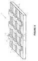
- FIG. 4shows a memory cell array 70 that includes rows 72 of an electrically conductive material, such as doped silicon (Si), or metal on doped Si; and columns 74 of an electrically conductive material, such as doped Si or metal on doped Si, deposited on a base layer 75 , such as polyamide, glass, or silicon.
- a gate dielectric layer 78is formed beneath the columns 74 .
- the gate dielectric layer 78is composed of a layer of electrically resistive viscoelastic carrier material with particles 76 dispersed in it and optionally, a good dielectric layer impervious to the particles.
- a three-terminal memory cell 77is formed by each adjacent pair of the rows 72 and an intersecting one of the columns 74 .
- Each memory cell 77can be embodied as either a fuse or anti-fuse transistor having a gate electrode 74 and an underlying gate dielectric layer 78 flanked by adjacent row conductors 72 that function as drain and source electrodes, respectively.
- a high voltage applied to the gate electrode 74 of an individual memory cell 77will cause the particles 76 dispersed in the underlying gate dielectric layer 78 to agglomerate or fuse together, thereby changing the current-voltage (IV) characteristics of the transistor formed by the gate, source, and drain electrodes.
- IVcurrent-voltage
- These shiftscan be used to store data in the memory cells 77 .
- any suitable current and/or voltage sensing or detection circuitrycan be utilized to measure or detect current, voltage, and/or resistance changes brought about by changes in the IV characteristics of the individual memory cells 77 . The measurements are used to read the data stored in the memory cells 77 .
- different voltagescan be applied to neighboring rows 72 to produce a field gradient which causes a change in the gate capacitance due to migration of the particles 76 .
- the changes in the gate capacitance of individual memory cells 77can be detected by source-drain current measurements
- the detection circuitry 81can be utilized to measure or detect the source-drain current of the individual memory cells 77 .
- the gate and a first electrodeare held at a write voltage while the second electrode is held at ground, the particles will move in the gate dielectric layer near the second electrode, thereby altering the field due to the gate near the second electrode.
- this second electrodeis biased to act as a source, the corresponding source-drain current for a given gate voltage is changed.
- the first electrodeis biased to serve as the source, the source-drain current is relatively unaffected. Because of the source-drain symmetry, the characteristics of this second case can be changed when the gate and second electrode are held at a write voltage and the first electrode is held at ground. Therefore, two bits of information can be written in each transistor.
Landscapes
- Physics & Mathematics (AREA)
- Condensed Matter Physics & Semiconductors (AREA)
- General Physics & Mathematics (AREA)
- Engineering & Computer Science (AREA)
- Computer Hardware Design (AREA)
- Microelectronics & Electronic Packaging (AREA)
- Power Engineering (AREA)
- Semiconductor Memories (AREA)
Abstract
Description
Claims (48)
Priority Applications (1)
| Application Number | Priority Date | Filing Date | Title |
|---|---|---|---|
| US10/285,802US6807079B2 (en) | 2002-11-01 | 2002-11-01 | Device having a state dependent upon the state of particles dispersed in a carrier |
Applications Claiming Priority (1)
| Application Number | Priority Date | Filing Date | Title |
|---|---|---|---|
| US10/285,802US6807079B2 (en) | 2002-11-01 | 2002-11-01 | Device having a state dependent upon the state of particles dispersed in a carrier |
Publications (2)
| Publication Number | Publication Date |
|---|---|
| US20040085797A1 US20040085797A1 (en) | 2004-05-06 |
| US6807079B2true US6807079B2 (en) | 2004-10-19 |
Family
ID=32175260
Family Applications (1)
| Application Number | Title | Priority Date | Filing Date |
|---|---|---|---|
| US10/285,802Expired - Fee RelatedUS6807079B2 (en) | 2002-11-01 | 2002-11-01 | Device having a state dependent upon the state of particles dispersed in a carrier |
Country Status (1)
| Country | Link |
|---|---|
| US (1) | US6807079B2 (en) |
Cited By (13)
| Publication number | Priority date | Publication date | Assignee | Title |
|---|---|---|---|---|
| US20060028895A1 (en)* | 2004-08-09 | 2006-02-09 | Carl Taussig | Silver island anti-fuse |
| US7026692B1 (en)* | 2003-11-12 | 2006-04-11 | Xilinx, Inc. | Low voltage non-volatile memory transistor |
| US20070045728A1 (en)* | 2005-08-24 | 2007-03-01 | Samsung Electronics Co., Ltd. | Non-volatile semiconductor memory device having ion conductive layer and methods of fabricating and operating the same |
| US20080185578A1 (en)* | 2007-02-02 | 2008-08-07 | Semiconductor Energy Laboratory Co., Ltd. | Memory Device |
| US20090081431A1 (en)* | 2007-06-08 | 2009-03-26 | Valtion Teknillinen Tutkimuskeskus | Structures based on nanoparticles and method for their fabrication |
| US20090224323A1 (en)* | 2008-03-06 | 2009-09-10 | Xilinx, Inc. | Integrated circuit with mosfet fuse element |
| US7710813B1 (en) | 2008-03-05 | 2010-05-04 | Xilinx, Inc. | Electronic fuse array |
| US7724600B1 (en) | 2008-03-05 | 2010-05-25 | Xilinx, Inc. | Electronic fuse programming current generator with on-chip reference |
| US7834659B1 (en) | 2008-03-05 | 2010-11-16 | Xilinx, Inc. | Multi-step programming of E fuse cells |
| US7888771B1 (en) | 2007-05-02 | 2011-02-15 | Xilinx, Inc. | E-fuse with scalable filament link |
| US7923811B1 (en) | 2008-03-06 | 2011-04-12 | Xilinx, Inc. | Electronic fuse cell with enhanced thermal gradient |
| US8642460B2 (en) | 2011-06-08 | 2014-02-04 | International Business Machines Corporation | Semiconductor switching device and method of making the same |
| US20220285520A1 (en)* | 2018-03-12 | 2022-09-08 | Soitec | Process for preparing a thin layer of ferroelectric material |
Families Citing this family (18)
| Publication number | Priority date | Publication date | Assignee | Title |
|---|---|---|---|---|
| DE102005009511B3 (en)* | 2005-02-24 | 2006-12-14 | Infineon Technologies Ag | A semiconductor memory device and method of manufacturing a semiconductor memory device |
| US7958120B2 (en) | 2005-05-10 | 2011-06-07 | Netseer, Inc. | Method and apparatus for distributed community finding |
| US9110985B2 (en)* | 2005-05-10 | 2015-08-18 | Neetseer, Inc. | Generating a conceptual association graph from large-scale loosely-grouped content |
| WO2007084778A2 (en) | 2006-01-19 | 2007-07-26 | Llial, Inc. | Systems and methods for creating, navigating and searching informational web neighborhoods |
| WO2007100923A2 (en)* | 2006-02-28 | 2007-09-07 | Ilial, Inc. | Methods and apparatus for visualizing, managing, monetizing and personalizing knowledge search results on a user interface |
| US9011762B2 (en)* | 2006-07-21 | 2015-04-21 | Valtion Teknillinen Tutkimuskeskus | Method for manufacturing conductors and semiconductors |
| US9817902B2 (en) | 2006-10-27 | 2017-11-14 | Netseer Acquisition, Inc. | Methods and apparatus for matching relevant content to user intention |
| WO2008059940A1 (en)* | 2006-11-17 | 2008-05-22 | Semiconductor Energy Laboratory Co., Ltd. | Memory element and method for manufacturing the same, and semiconductor device |
| FI122011B (en) | 2007-06-08 | 2011-07-15 | Teknologian Tutkimuskeskus Vtt | Method for Producing an Electronic Module, Intermediate to Produce an Electronic Module, Memory Element, Printed Electronic Product, Sensor Device, and RFID Tag |
| FI122014B (en) | 2007-06-08 | 2011-07-15 | Teknologian Tutkimuskeskus Vtt | Method and apparatus for the functionalization of nanoparticle systems |
| FI122644B (en)* | 2007-06-08 | 2012-04-30 | Teknologian Tutkimuskeskus Vtt | Process for forming electrically conductive or semiconducting paths on a substrate and using the method for producing transistors and producing sensors |
| US10387892B2 (en)* | 2008-05-06 | 2019-08-20 | Netseer, Inc. | Discovering relevant concept and context for content node |
| US20090300009A1 (en)* | 2008-05-30 | 2009-12-03 | Netseer, Inc. | Behavioral Targeting For Tracking, Aggregating, And Predicting Online Behavior |
| US8417695B2 (en)* | 2008-10-30 | 2013-04-09 | Netseer, Inc. | Identifying related concepts of URLs and domain names |
| US10311085B2 (en) | 2012-08-31 | 2019-06-04 | Netseer, Inc. | Concept-level user intent profile extraction and applications |
| CN104218028B (en)* | 2013-06-05 | 2018-03-30 | 中芯国际集成电路制造(上海)有限公司 | ESD-protection structure and forming method thereof |
| US10714242B2 (en)* | 2017-12-20 | 2020-07-14 | International Business Machines Corporation | Symmetrically tunable electrical resistor |
| CN110564406A (en)* | 2019-03-14 | 2019-12-13 | 浙江精一新材料科技有限公司 | Quantum dot modified TiO2the synthesis method of the hybrid nano-rod and the optical transmission control device using the synthesis method |
Citations (5)
| Publication number | Priority date | Publication date | Assignee | Title |
|---|---|---|---|---|
| US4922319A (en)* | 1985-09-09 | 1990-05-01 | Fujitsu Limited | Semiconductor programmable memory device |
| US5444290A (en)* | 1994-05-26 | 1995-08-22 | Symetrix Corporation | Method and apparatus for programming antifuse elements using combined AC and DC electric fields |
| US5811870A (en)* | 1997-05-02 | 1998-09-22 | International Business Machines Corporation | Antifuse structure |
| US5834824A (en)* | 1994-02-08 | 1998-11-10 | Prolinx Labs Corporation | Use of conductive particles in a nonconductive body as an integrated circuit antifuse |
| US6418049B1 (en)* | 1997-12-04 | 2002-07-09 | Arizona Board Of Regents | Programmable sub-surface aggregating metallization structure and method of making same |
- 2002
- 2002-11-01USUS10/285,802patent/US6807079B2/ennot_activeExpired - Fee Related
Patent Citations (6)
| Publication number | Priority date | Publication date | Assignee | Title |
|---|---|---|---|---|
| US4922319A (en)* | 1985-09-09 | 1990-05-01 | Fujitsu Limited | Semiconductor programmable memory device |
| US5834824A (en)* | 1994-02-08 | 1998-11-10 | Prolinx Labs Corporation | Use of conductive particles in a nonconductive body as an integrated circuit antifuse |
| US5444290A (en)* | 1994-05-26 | 1995-08-22 | Symetrix Corporation | Method and apparatus for programming antifuse elements using combined AC and DC electric fields |
| US5811870A (en)* | 1997-05-02 | 1998-09-22 | International Business Machines Corporation | Antifuse structure |
| US6344373B1 (en)* | 1997-05-02 | 2002-02-05 | International Business Machines Corporation | Antifuse structure and process |
| US6418049B1 (en)* | 1997-12-04 | 2002-07-09 | Arizona Board Of Regents | Programmable sub-surface aggregating metallization structure and method of making same |
Cited By (20)
| Publication number | Priority date | Publication date | Assignee | Title |
|---|---|---|---|---|
| US7026692B1 (en)* | 2003-11-12 | 2006-04-11 | Xilinx, Inc. | Low voltage non-volatile memory transistor |
| US20060134839A1 (en)* | 2003-11-12 | 2006-06-22 | Xilinx, Inc. | Low voltage non-volatile memory transistor |
| US7092273B2 (en)* | 2003-11-12 | 2006-08-15 | Xilinx Inc. | Low voltage non-volatile memory transistor |
| US20060028895A1 (en)* | 2004-08-09 | 2006-02-09 | Carl Taussig | Silver island anti-fuse |
| US20070045728A1 (en)* | 2005-08-24 | 2007-03-01 | Samsung Electronics Co., Ltd. | Non-volatile semiconductor memory device having ion conductive layer and methods of fabricating and operating the same |
| US8193569B2 (en) | 2005-08-24 | 2012-06-05 | Samsung Electronics Co., Ltd. | Non-volatile semiconductor memory device having ion conductive layer and methods of fabricating and operating the same |
| US20080185578A1 (en)* | 2007-02-02 | 2008-08-07 | Semiconductor Energy Laboratory Co., Ltd. | Memory Device |
| US9006741B2 (en)* | 2007-02-02 | 2015-04-14 | Semiconductor Energy Laboratory Co., Ltd. | Memory device in a programmed state having a memory layer comprising conductive nanoparticles coated with an organic film formed between two conductive layers |
| US7888771B1 (en) | 2007-05-02 | 2011-02-15 | Xilinx, Inc. | E-fuse with scalable filament link |
| US20090081431A1 (en)* | 2007-06-08 | 2009-03-26 | Valtion Teknillinen Tutkimuskeskus | Structures based on nanoparticles and method for their fabrication |
| US8029722B2 (en)* | 2007-06-08 | 2011-10-04 | Valtion Teknillinen Tutkimuskeskus | Method of fabricating structures based on nanoparticles |
| US7834659B1 (en) | 2008-03-05 | 2010-11-16 | Xilinx, Inc. | Multi-step programming of E fuse cells |
| US7724600B1 (en) | 2008-03-05 | 2010-05-25 | Xilinx, Inc. | Electronic fuse programming current generator with on-chip reference |
| US7710813B1 (en) | 2008-03-05 | 2010-05-04 | Xilinx, Inc. | Electronic fuse array |
| US7923811B1 (en) | 2008-03-06 | 2011-04-12 | Xilinx, Inc. | Electronic fuse cell with enhanced thermal gradient |
| US8564023B2 (en) | 2008-03-06 | 2013-10-22 | Xilinx, Inc. | Integrated circuit with MOSFET fuse element |
| US20090224323A1 (en)* | 2008-03-06 | 2009-09-10 | Xilinx, Inc. | Integrated circuit with mosfet fuse element |
| US8642460B2 (en) | 2011-06-08 | 2014-02-04 | International Business Machines Corporation | Semiconductor switching device and method of making the same |
| US20220285520A1 (en)* | 2018-03-12 | 2022-09-08 | Soitec | Process for preparing a thin layer of ferroelectric material |
| US12300737B2 (en)* | 2018-03-12 | 2025-05-13 | Soitec | Process for preparing a thin layer of ferroelectric material |
Also Published As
| Publication number | Publication date |
|---|---|
| US20040085797A1 (en) | 2004-05-06 |
Similar Documents
| Publication | Publication Date | Title |
|---|---|---|
| US6807079B2 (en) | Device having a state dependent upon the state of particles dispersed in a carrier | |
| US6781868B2 (en) | Molecular memory device | |
| US7183141B1 (en) | Reversible field-programmable electric interconnects | |
| KR100885276B1 (en) | Floating Gate Memory Devices Using Complex Molecular Materials | |
| US7145793B1 (en) | Electrically addressable memory switch | |
| US7274587B2 (en) | Semiconductor memory element and semiconductor memory device | |
| US7113420B2 (en) | Molecular memory cell | |
| US6072716A (en) | Memory structures and methods of making same | |
| US8101976B2 (en) | Device selection circuitry constructed with nanotube ribbon technology | |
| US20100078758A1 (en) | Miim diodes | |
| CN101681913B (en) | Variable resistance element, manufacturing method thereof, and nonvolatile semiconductor memory device | |
| US6836424B2 (en) | Hybrid circuit having nanotube electromechanical memory | |
| TW556340B (en) | Memory device having dual tunnel junction memory cells | |
| US7239542B2 (en) | Storage apparatus | |
| US8264868B2 (en) | Memory array with metal-insulator transition switching devices | |
| US20040090823A1 (en) | Low-energy writing in cross-point array memory devices | |
| KR20030014653A (en) | One-time programmable memory using fuse/anti-fuse and vertically oriented fuse unit memory cells | |
| CN103098211B (en) | multi-tier storage array | |
| US20170179131A1 (en) | Semiconductor integrated circuit | |
| WO2008065558A1 (en) | Memory device and method for fabricating a memory device | |
| US20170155045A1 (en) | Method to Manufacture Highly Conductive Vias and PROM Memory Cells by Application of Electric Pulses |
Legal Events
| Date | Code | Title | Description |
|---|---|---|---|
| AS | Assignment | Owner name:HEWLETT-PACKARD DEVELOPMENT COMPANY, L.P., TEXAS Free format text:ASSIGNMENT OF ASSIGNORS INTEREST;ASSIGNORS:MEI, PING;JACKSON, WARREN;REEL/FRAME:014037/0780 Effective date:20020723 | |
| AS | Assignment | Owner name:HEWLETT-PACKARD DEVELOPMENT COMPANY, L.P., COLORADO Free format text:ASSIGNMENT OF ASSIGNORS INTEREST;ASSIGNOR:HEWLETT-PACKARD COMPANY;REEL/FRAME:013776/0928 Effective date:20030131 Owner name:HEWLETT-PACKARD DEVELOPMENT COMPANY, L.P., COLORAD Free format text:ASSIGNMENT OF ASSIGNORS INTEREST;ASSIGNOR:HEWLETT-PACKARD COMPANY;REEL/FRAME:013776/0928 Effective date:20030131 Owner name:HEWLETT-PACKARD DEVELOPMENT COMPANY, L.P.,COLORADO Free format text:ASSIGNMENT OF ASSIGNORS INTEREST;ASSIGNOR:HEWLETT-PACKARD COMPANY;REEL/FRAME:013776/0928 Effective date:20030131 | |
| FPAY | Fee payment | Year of fee payment:4 | |
| REMI | Maintenance fee reminder mailed | ||
| FPAY | Fee payment | Year of fee payment:8 | |
| AS | Assignment | Owner name:HEWLETT PACKARD ENTERPRISE DEVELOPMENT LP, TEXAS Free format text:ASSIGNMENT OF ASSIGNORS INTEREST;ASSIGNOR:HEWLETT-PACKARD DEVELOPMENT COMPANY, L.P.;REEL/FRAME:037079/0001 Effective date:20151027 | |
| REMI | Maintenance fee reminder mailed | ||
| LAPS | Lapse for failure to pay maintenance fees | ||
| STCH | Information on status: patent discontinuation | Free format text:PATENT EXPIRED DUE TO NONPAYMENT OF MAINTENANCE FEES UNDER 37 CFR 1.362 | |
| FP | Lapsed due to failure to pay maintenance fee | Effective date:20161019 |