US6806991B1 - Fully released MEMs XYZ flexure stage with integrated capacitive feedback - Google Patents
Fully released MEMs XYZ flexure stage with integrated capacitive feedbackDownload PDFInfo
- Publication number
- US6806991B1 US6806991B1US10/219,044US21904402AUS6806991B1US 6806991 B1US6806991 B1US 6806991B1US 21904402 AUS21904402 AUS 21904402AUS 6806991 B1US6806991 B1US 6806991B1
- Authority
- US
- United States
- Prior art keywords
- stage
- fully
- released
- micro
- actuators
- Prior art date
- Legal status (The legal status is an assumption and is not a legal conclusion. Google has not performed a legal analysis and makes no representation as to the accuracy of the status listed.)
- Expired - Fee Related, expires
Links
- 239000000523sampleSubstances0.000claimsdescription13
- 229910001285shape-memory alloyInorganic materials0.000claimsdescription2
- 230000008878couplingEffects0.000abstractdescription7
- 238000010168coupling processMethods0.000abstractdescription7
- 238000005859coupling reactionMethods0.000abstractdescription7
- 239000000758substrateSubstances0.000abstractdescription7
- 238000000034methodMethods0.000description17
- 238000006073displacement reactionMethods0.000description16
- 238000004519manufacturing processMethods0.000description13
- 230000008901benefitEffects0.000description7
- 230000005641tunnelingEffects0.000description7
- 238000013461designMethods0.000description6
- 230000008569processEffects0.000description6
- 230000007246mechanismEffects0.000description4
- VYPSYNLAJGMNEJ-UHFFFAOYSA-NSilicium dioxideChemical compoundO=[Si]=OVYPSYNLAJGMNEJ-UHFFFAOYSA-N0.000description3
- 238000010438heat treatmentMethods0.000description3
- 239000000203mixtureSubstances0.000description3
- 230000003287optical effectEffects0.000description3
- XUIMIQQOPSSXEZ-UHFFFAOYSA-NSiliconChemical compound[Si]XUIMIQQOPSSXEZ-UHFFFAOYSA-N0.000description2
- 238000001514detection methodMethods0.000description2
- 238000005530etchingMethods0.000description2
- 230000006870functionEffects0.000description2
- 238000003384imaging methodMethods0.000description2
- 238000005259measurementMethods0.000description2
- 238000003199nucleic acid amplification methodMethods0.000description2
- 238000012545processingMethods0.000description2
- 230000004044responseEffects0.000description2
- 229910052710siliconInorganic materials0.000description2
- 239000010703siliconSubstances0.000description2
- 208000005647MumpsDiseases0.000description1
- 230000004075alterationEffects0.000description1
- 230000003321amplificationEffects0.000description1
- 238000004873anchoringMethods0.000description1
- 230000004888barrier functionEffects0.000description1
- 239000003990capacitorSubstances0.000description1
- 230000008859changeEffects0.000description1
- 238000010276constructionMethods0.000description1
- 230000003247decreasing effectEffects0.000description1
- 238000010586diagramMethods0.000description1
- 230000000694effectsEffects0.000description1
- 238000003780insertionMethods0.000description1
- 230000037431insertionEffects0.000description1
- 238000005304joiningMethods0.000description1
- 239000000463materialSubstances0.000description1
- 238000000691measurement methodMethods0.000description1
- 238000010297mechanical methods and processMethods0.000description1
- 239000002184metalSubstances0.000description1
- 238000005459micromachiningMethods0.000description1
- 208000010805mumps infectious diseaseDiseases0.000description1
- 230000008520organizationEffects0.000description1
- 238000000926separation methodMethods0.000description1
- 235000012239silicon dioxideNutrition0.000description1
- 239000000377silicon dioxideSubstances0.000description1
- 229910052814silicon oxideInorganic materials0.000description1
- 238000006467substitution reactionMethods0.000description1
Images


Classifications
- G—PHYSICS
- G01—MEASURING; TESTING
- G01Q—SCANNING-PROBE TECHNIQUES OR APPARATUS; APPLICATIONS OF SCANNING-PROBE TECHNIQUES, e.g. SCANNING PROBE MICROSCOPY [SPM]
- G01Q10/00—Scanning or positioning arrangements, i.e. arrangements for actively controlling the movement or position of the probe
- G01Q10/04—Fine scanning or positioning
- G—PHYSICS
- G02—OPTICS
- G02B—OPTICAL ELEMENTS, SYSTEMS OR APPARATUS
- G02B26/00—Optical devices or arrangements for the control of light using movable or deformable optical elements
- G02B26/08—Optical devices or arrangements for the control of light using movable or deformable optical elements for controlling the direction of light
- G02B26/0816—Optical devices or arrangements for the control of light using movable or deformable optical elements for controlling the direction of light by means of one or more reflecting elements
- G02B26/0833—Optical devices or arrangements for the control of light using movable or deformable optical elements for controlling the direction of light by means of one or more reflecting elements the reflecting element being a micromechanical device, e.g. a MEMS mirror, DMD
- G02B26/0841—Optical devices or arrangements for the control of light using movable or deformable optical elements for controlling the direction of light by means of one or more reflecting elements the reflecting element being a micromechanical device, e.g. a MEMS mirror, DMD the reflecting element being moved or deformed by electrostatic means
Definitions
- the present inventionis in general related to manipulation of a stage and, more particularly, to manipulation of a fully released stage in a decoupled manner according to closed-loop feedback with sub-micron accuracy.
- Scanning probe microscopesare devices which manipulate a scanning probe with sub-atomic accuracy to scan the surface of a sample object or material.
- the scanning tunneling microscopeSTM is a solid-state microscope based on the principle of quantum mechanical tunneling of electrons between a sharp tip and a conducting sample.
- the tip of an STMis an extremely sharp metal tip.
- the tipis mounted on a system of piezoelectric drives which are controllable with sub-atomic precision.
- the scanning processbegins by bringing the tip within a few Angstroms of the conducting sample surface. At such separations, the outer electron orbitals of the tip and the sample overlap.
- FIG. 1Adepicts a block diagram of a typical SPM 100 according to the prior art.
- the sample 103 to be scannedis placed on stage 102 .
- Control means 105causes a suitable voltage to be applied to piezo element 104 .
- piezo element 104controllably expands.
- the expansionmay occur in any of the X-direction, Y-direction, and Z-direction.
- control means 105controls the vertical distance (in the Z-direction) between scanning tip 101 and sample 103 .
- control means 105causes piezo element 104 to move scanning tip 101 over sample 103 according to, for example, a raster pattern in the X and Y-directions.
- the control of piezo element 104may utilize various feedback techniques such as examining the tunneling current associated with scanning tip 101 . Also, other feedback techniques may be utilized such as optical feedback, capacitive feedback, and piezo-resistive feedback (not shown).
- the imaging signal associated with scanning tip 101may be provided to imaging system 106 for suitable processing.
- the dimensions of SPM 100are typically on the order of ten centimeters. Accordingly, the scanable area of an object placed on stage 102 is quite small relative to the size of SPM 100 .
- FIG. 1Bdepicts XY stage 150 according to the prior art which is operable to control lens 155 .
- XY stage 150comprises a plurality of cascaded thermal actuators ( 151 - 154 ).
- the thermal actuators ( 151 - 154 )are mechanically coupled to lens 155 via respective general purpose flexures which are generally known for use to facilitate actuation in Micro-Electrical-Mechanical (MEMs) devices.
- MEMsMicro-Electrical-Mechanical
- Actuators 152 and 154enable displacement of lens 155 in the Y-direction and actuators 151 and 153 enable displacement of lens 155 in the X-direction.
- the design of XY stage 150does not fully decouple the manipulation of lens 155 in the X and Y directions. Specifically, displacement of lens 155 in the X-direction by actuators 151 and 153 will also cause some amount of displacement in the Y-direction. Likewise, displacement of lens 155 in the Y-direction by actuators 152 and 154 will also cause some amount of displacement in the X-direction.
- known structures that manipulate high resolution XYZ stageseither (1) are associated with coupled movement where actuation in one direction causes a lesser degree of actuation in another direction; (2) require bulky piezo elements to achieve the desired non-coupled movement; or (3) are permanently anchored to the substrate on which they were fabricated.
- flip-chip bondingis well-known in the art for bonding two discrete structures after fabrication of the structures.
- flip-chip bondingis problematic, because it imposes a relatively simple mechanical design via the bonding of a first flat surface to a second flat surface.
- flip-chip bondingprevents assembly of structures with surface features and, hence, reduces the potential complexity of devices assembled utilizing this technique.
- the present inventionis directed to a system and method which are operable to manipulate a fully released stage to provide decoupled movement that is controlled by suitable closed-loop feedback.
- the XY positioning of the stagemay be advantageously manipulated using a first plurality of actuators (e.g., comb drives, parallel plate actuators, shaped memory alloy (SMA) actuators, electrothermal actuators, piezo stack actuators, and/or the like) and a second plurality of actuators.
- the actuatorsare implemented as flexure amplified banks of bent beams that each occupy approximately 400 microns in length. By utilizing actuators of this scale, the total size of the device may be significantly reduced. In embodiments of the present invention, the entire device may be approximately one millimeter in length.
- the actuatorsmay be advantageously coupled to flexures which are, in turn, coupled to the stage.
- the actuators and the flexuresare positioned and operate in a mirrored manner. Specifically, when it is desired to actuate the stage in the X-direction, two corresponding mirrored actuators are supplied current. The actuators move the stage in the desired direction via the coupled flexures. It shall be appreciated that the same actuators that cause the actuation in the X-direction may also produce undesired forces in the Y-direction. If the undesired forces are not addressed by embodiments of the present invention, the forces will produce coupled movement. However, embodiments of the present invention utilize the mirrored positioning and flexures to balance the undesired forces in the Y-direction.
- Actuation in the Y-directionmay also utilize a mirror positioning and operation of movements to decouple movement in the Y-direction. Thus, actuation in the X-direction and the Y-direction are fully decoupled.
- a third actuatormay also be utilized to actuate the stage in the Z-direction.
- suitable feedback structurescapacitor, optical, piezo-resistive, and/or the like may be utilized to control the manipulation of the stage.
- FIG. 1Adepicts a scanning tunneling microscope according to the prior art
- FIG. 1Bis a cascaded XY stage that manipulates a micro-lens according to the prior art
- FIG. 2depicts an XY stage according to embodiments of the present invention
- FIG. 3depicts a base structure that provides quadrant capacitive feedback according to embodiments of the present invention
- FIG. 4depicts an XYZ stage system that provides interdigitated differential feedback according to embodiments of the present invention
- FIG. 5depicts a fabrication stage where an XY stage is fabricated on top of a silicon oxide sacrificial layer according to embodiments of the present invention
- FIG. 6Adepicts a base structure that is suitable to be mechanically coupled to an XY stage according to embodiments of the present invention
- FIG. 6Bdepicts a snap connector according to embodiments of the present invention.
- FIG. 7depicts a base structure mechanically coupled to an XY stage according to embodiments of the present invention.
- FIG. 8Adepicts an XY stage mechanically coupled to a base structure and released from a silicon substrate according to embodiments of the present invention
- FIG. 8Bdepicts a payload structure mechanically coupled to the XY stage and base structure shown in FIG. 8A;
- FIG. 9depicts an array of XYZ stages according to embodiments of the present invention.
- FIGS. 10-19depicts actuators that exhibit motion amplification utilizing anchored flexures according to embodiments of the present invention.
- FIG. 2depicts system 200 that manipulates XY stage 202 according to embodiments of the present invention.
- System 200comprises a plurality of flexures ( 201 a , 201 b , 201 c , and 201 d ) that are mechanically coupled to XY stage 202 .
- Flexures 201 a , 201 b , 201 c , and 201 dare structural elements that are relatively flexible in one direction and are relatively stiff in the other direction.
- Flexures 201 a - 201 dmay comprise a plurality of “bends” which provide the desired flexibility and stiffness in orthogonal directions. For example, as shown in FIG. 2, flexure 201 a is relatively flexible in the Y-direction.
- flexure 201 aApplication of a force in the Y-direction on flexure 201 a will tend to deform the elements of flexure 201 a , i.e., flexure 201 a either expands or compresses.
- flexure 201 ais relatively stiff in the X-direction. Accordingly, application of a force in the X-direction tends to displace flexure 201 a instead of deforming the elements of flexure 201 a .
- the design of flexures 201 a - 201 d as shown in FIG. 2is merely exemplary and other flexure designs may be utilized according to embodiments of the present invention.
- Flexures 201 a , 201 b , 201 c , and 201 dare mechanically coupled to actuators 203 a , 203 b , 203 c , and 203 d which may be implemented as, for example, stacked sets of thermal elements.
- actuators 203 a , 203 b , 203 c , and 203 dwhich may be implemented as, for example, stacked sets of thermal elements.
- the thermal elementsexperience Ohmic heating. The heating causes differential displacement of the thermal elements causing actuation in the desired direction.
- flexures 201 a , 201 b , 201 c , and 201 dmay be associated with anchor elements 205 a - 205 d .
- Anchor elements 205 a - 205 dmay amplify the displacement associated with actuators 203 a - 203 d as will be discussed in greater detail with respect to FIG. 10 . Also, it shall be appreciated that, when actuators are coupled with anchor elements 205 a - 205 d , actuators 203 a - 203 d are not purely linear devices. For example, application of current to actuator 203 a will cause actuation primarily in the X-direction and, to a lesser degree, will cause actuation in the Y-direction. Other suitable actuators may also be utilized such as electrostatic actuators.
- Actuators 203 a - 203 d and flexures 201 a - 201 dare disposed in and operate in a “mirrored” fashion to compensate for the non-linear characteristics of actuators 203 a - 203 d coupled with anchor elements 205 a - 205 d .
- actuators 203 a , 203 c and flexures 201 a , 201 cenable displacement of XY stage 202 in the X-direction.
- currentis supplied to both of actuators 203 a and 203 c .
- flexures 201 a and 201 care relatively stiff with respect to the X-direction, the displacement generated by actuators 203 a and 203 c causes a force to be transmitted to XY stage 202 via flexures 201 a and 201 c .
- application of currentcauses actuators 203 a and 203 c coupled with anchor elements 205 a and 205 c to generate forces in the Y-direction.
- the force generated by actuator 203 a in the Y-directionis balanced by the force generated by actuators 203 c in the Y-direction.
- the total torque applied to XY stage 202is zero due to the mirrored configuration and operation.
- actuators 203 b and 203 d and flexures 201 b and 201 dare disposed in and operate in a mirrored manner as actuators 203 a - 203 d and flexures 201 a - 201 d . Accordingly, actuation in both of the X-direction and Y-direction is fully decoupled.
- XY stage system 200may be mechanically coupled to a base structure which provides closed-loop feedback.
- closed-loop feedbackembodiments of the present invention enable XY stage 202 to be repeatedly positioned at a specified location. This type of functionality may be advantageous for numerous applications such as scanning electron microscopes, tunneling electron microscopes, atomic force microscopes, and nano or micro fabrication process systems.
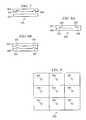
- FIG. 3depicts structure 300 that includes a plurality of capacitive elements ( 301 , 302 , 303 , and 304 ) to implement quadrant capacitive feedback.
- capacitive elements 301 - 304may be fabricated on a base structure to which system 200 may be mechanically coupled to collectively form structure 300 .
- XY stage 202When XY stage 202 is translated, the amount of overlap between XY stage 202 and the respective capacitive elements 301 through 304 changes.
- the capacitance associated with a respective capacitive element and XY stage 202is related to the amount of overlap, measuring the capacitance associated with each of capacitive elements 301 through 304 in response to an applied alternating circuit signal permits the XY position of XY stage 202 to be determined. Furthermore, the Z position of XY stage 202 relative to base structure 300 may be determined by summing the capacitance associated with capacitive elements 301 through 304 .
- a differential capacitive arrangementmay be utilized to provide positioning feedback.
- System 400 of FIG. 4comprises a plurality of interdigitated capacitive electrode sets ( 401 , 402 , 403 , 404 ) which are mechanically coupled to stage 202 .
- a corresponding base structure(not shown) may comprise corresponding interdigitated capacitive electrode sets.
- signal noiseis often the limiting factor in obtaining a high resolution measurement.
- Differential measurement techniquesare often utilized to eliminate “common mode” noise (i.e., the noise that is common to two inputs).
- the capacitive electrode setsare placed such that one set of interdigitated capacitors is increasing while the other set is decreasing, so that one signal may be subtracted from the other (the common mode noise cancels out) to obtain the capacitance measurement.
- XY stagesmay be fabricated as fully released structures utilizing surface micro-machining techniques such as the Multi-User Micro-Electro-Mechanical process (MUMPs process).
- FIG. 5depicts exemplary fabrication stage 500 according to embodiments of the present invention.
- Fabrication stage 500comprises XY stage system 501 fabricated on sacrificial layer 502 of silicon dioxide that is deposited on silicon substrate 503 .
- XY stage 501may be designed to be mechanically coupled to a suitable base structure such as base structure 600 of FIG. 6A via receptacles 504 .
- Base structure 600may comprise corresponding coupling elements 601 to mechanically couple to XY stage system 501 .
- Coupling elements 601may be implemented as “snap connectors” as disclosed in co-pending and commonly assigned U.S. patent application Ser. No. 09/570,170 entitled “System and Method for Coupling Micro-Components,” which is incorporated herein by reference.
- An example of snap connector 650is provided in FIG. 6 B.
- the snap connectormay comprise opposing latching arms that apply a spring force when deflected.
- the latching armsmay be preloaded by bringing the opposing latching arms closer together.
- the latching armsmay remain in the preloaded position by utilizing a suitable cocking mechanism.
- the latching armsmay be inserted into a suitable corresponding receptacle.
- the snap connectormay further comprise a triggering mechanism.
- the latching armsWhen the triggering mechanism is contacted during insertion of the snap connector into the receptacle, the latching arms are released from the preloaded state and return to their equilibrium position. Moreover, the latching arms may comprise suitable barbs to retain the latching arms in the receptacle thereby facilitating the desired mechanical coupling.
- snap connectorsare advantageous for assembly operations, it shall be appreciated that embodiments of the present invention are not limited to snap connections. Any other suitable coupling mechanism may be utilized such as metallic bonding elements.
- Base structure 600may comprise a plurality of power pads 602 to provide current to actuators of XY stage system 501 and any other suitable electrical elements (not shown). Also, base structure 600 may comprise electrostatic element 603 . Electrostatic element 603 may be utilized to apply an electrostatic force to the XY stage 202 of XY stage system 501 to actuate XY stage 202 in the Z-direction. As previously noted, base structure 600 may comprise feedback elements 604 .
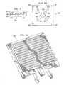
- FIG. 7depicts fabrication stage 700 which comprises XY stage system 501 released from substrate 503 after application of the suitable etching solution.
- FIG. 8Adepicts XY stage system 501 mechanically coupled to base structure 600 via the snap connectors and receptacles of XY stage system 501 and base structure 600 . Together XY stage system 501 and base structure 600 provide a fully released XYZ stage that provides decoupled actuation and closed loop feedback.
- payload 850 or other structuremay be assembled on to XY stage system 501 in a similar manner as shown in FIG. 8 B.
- suitable snap connectors 601 or other connectorsmay be utilized to mechanically coupled payload 850 to XY stage system 501 .
- a complex assemblymay be assembled according to embodiments of the present invention to comprise a stage assembled onto a capacitive detection substrate and a suitable device (e.g., lens, mirror, another XY stage) assembled onto the stage surface.
- Embodiments of the present inventionmay provide numerous advantages. Specifically, known structures that manipulate high resolution XYZ stages either (1) are associated with coupled movement where actuation in one direction causes a lesser degree of actuation in another direction; (2) require bulky piezo elements to achieve the desired non-coupled movement; or (3) are permanently anchored to the substrate on which they were fabricated. Embodiments of the present invention may dispose and operate thermal or electrostatic actuators in a mirrored manner to cause the actuation to be substantially decoupled. Moreover, the use of thermal or electrostatic actuators enables the size of the device to be greatly reduced. By reducing the size of the individual devices, embodiments of the present invention enable applications to be implemented that employ an array of XYZ stages according to embodiments of the present invention. FIG.
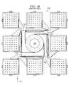
- FIG. 9depicts exemplary array 900 that includes a plurality of XYZ stages with each of the stages comprising suitable probe or manipulator 901 (e.g., a scanning tunneling tip, a gripper, and/or the like).
- suitable probe or manipulator 901e.g., a scanning tunneling tip, a gripper, and/or the like.
- the array of XYZ stagesmay be utilized to implement parallel nano or micro fabrication, parallel scanning of a surface, and/or any number of parallel processing applications.
- FIG. 10depicts flexure amplified thermal actuator 1000 according to embodiments of the present invention.
- Actuator 1000comprises a set of bent beams for actuation as is known in the art.
- An example of a bent beam actuator according to the prior artis described in U.S. Pat. No. 5,909,078.
- the bent beam portion of actuator 1001comprises thermal elements 1001 , anchors 1002 , and joining element 1004 .
- One set of thermal elementsis disposed on the “left” side of actuator 1000 and another set is disposed on the “right” side of actuator 1000 .
- the two sets of thermal elementsare joined in the middle by element 1004 .
- thermal elements 1001are anchored at their distal ends by anchors 1002 .
- Flexure 1005is mechanically coupled to element 1004 .
- thermal elements 1001When current is applied to thermal elements 1001 , thermal elements 1001 experience Ohmic heating and tend to expand. Due to anchors 1002 and element 1004 , the expansion of thermal elements 1001 causes actuation in direction 1006 . Specifically, the actuation is applied to flexure 1005 and is associated with a relatively high force and low displacement.
- Actuator 1000differs from known bent beam designs by anchoring flexure 1005 via anchor 1003 . This arrangement causes motion-amplification. Specifically, the actuation applied by thermal elements 1001 via element 1004 causes flexure 1005 to deform due to anchor 1003 . Thus, apex 1008 of flexure 1005 experiences a greater amount of displacement than is associated with element 1004 . Specifically actuator 1001 provides a greater amount of displacement as a function of device footprint as compared to known bent beam actuators. Curve 1007 shows the range of motion associated with displacement of apex 1008 during operation of actuator 1000 .
- Embodiments of the present inventionmay adapt actuator 1000 for use in a decoupled MEMs XY or XYZ stage by positioning corresponding actuators 1000 to compensate for the non-linear motion.
- actuator 1000is not limited to use in XY or XYZ stages. Actuator 1000 may be utilized in any suitable application that may benefit from motion-amplified actuation.
- FIG. 11depicts gripper 1100 .
- Gripper 1100is substantially similar to actuator 1000 .
- gripper 1100comprises two flexures 1005 and two anchors 1003 .
- a gripping element 1101is disposed at the end of both flexures 1005 .
- gripper 1100is operated (e.g., current is applied)
- flexures 1005displace and gripping elements 1101 separate. After current is no longer applied, flexures 1005 return to the original positions and gripping elements 1101 are brought closer together.
- a structure or device placed in between gripping elements 1101may then be suitably manipulated.
- this embodimentis merely exemplary. Any other suitable application may be implemented utilizing a motion-amplified actuator according to embodiments of the present invention.
- FIG. 12depicts an alternative configuration of actuator 1200 according to embodiments of the present invention.
- Actuator 1200is substantially similar to actuator 1000 .
- actuator 1200is disposed so that element 1004 is displaced in the opposite direction (direction 1201 ) as compared to the displacement of element 1004 in actuator 1000 . As shown in FIG. 12, this causes the range of motion of apex 1008 of flexure 1005 to follow curve 1202 .
- FIGS. 13-29depict other configurations that employ a motion-amplified bent beam actuator according to embodiments of the present invention.
- FIGS. 13-29depict other configurations that employ a motion-amplified bent beam actuator according to embodiments of the present invention.
- FIGS. 17 and 18depict motion amplified actuators which produce rotational displacement utilizing flexures 1005 and anchor 1003 according to embodiments of the present invention.
- FIG. 19depicts an out-of-plane design. Specifically, flexures 1005 extend away from bent beams 1002 in the same plane as bent beams 1002 . However, flexure portion 1003 is raised and anchored above flexure 1005 . Thus, out-of-plane amplified motion may be achieved according to embodiments of the present invention.
Landscapes
- Physics & Mathematics (AREA)
- General Physics & Mathematics (AREA)
- Health & Medical Sciences (AREA)
- General Health & Medical Sciences (AREA)
- Nuclear Medicine, Radiotherapy & Molecular Imaging (AREA)
- Radiology & Medical Imaging (AREA)
- Optics & Photonics (AREA)
- Micromachines (AREA)
Abstract
Description
Claims (25)
Priority Applications (1)
| Application Number | Priority Date | Filing Date | Title |
|---|---|---|---|
| US10/219,044US6806991B1 (en) | 2001-08-16 | 2002-08-14 | Fully released MEMs XYZ flexure stage with integrated capacitive feedback |
Applications Claiming Priority (2)
| Application Number | Priority Date | Filing Date | Title |
|---|---|---|---|
| US31270601P | 2001-08-16 | 2001-08-16 | |
| US10/219,044US6806991B1 (en) | 2001-08-16 | 2002-08-14 | Fully released MEMs XYZ flexure stage with integrated capacitive feedback |
Publications (1)
| Publication Number | Publication Date |
|---|---|
| US6806991B1true US6806991B1 (en) | 2004-10-19 |
Family
ID=33134640
Family Applications (1)
| Application Number | Title | Priority Date | Filing Date |
|---|---|---|---|
| US10/219,044Expired - Fee RelatedUS6806991B1 (en) | 2001-08-16 | 2002-08-14 | Fully released MEMs XYZ flexure stage with integrated capacitive feedback |
Country Status (1)
| Country | Link |
|---|---|
| US (1) | US6806991B1 (en) |
Cited By (54)
| Publication number | Priority date | Publication date | Assignee | Title |
|---|---|---|---|---|
| US20040129873A1 (en)* | 2002-12-20 | 2004-07-08 | Lindsay Stuart M. | Fast scanning stage for a scanning probe microscope |
| US20040196774A1 (en)* | 2002-02-21 | 2004-10-07 | Lg Electronics Inc. | Piezoelectric driving type tracking device and method for fabricating the same |
| US20050198844A1 (en)* | 2004-02-13 | 2005-09-15 | Lee Suk-Won | Stage apparatus |
| US20050237597A1 (en)* | 2004-04-27 | 2005-10-27 | Marc Epitaux | Electromechanical drives adapted to provide two degrees of mobility |
| US20060158484A1 (en)* | 2005-01-14 | 2006-07-20 | Greywall Dennis S | Thermal actuator for a MEMS device |
| US20060221430A1 (en)* | 2005-04-05 | 2006-10-05 | Samsung Electronics Co. , Ltd. | Versatile system for a locking electro-thermal actuated MEMS switch |
| US20070028714A1 (en)* | 2005-07-29 | 2007-02-08 | Brigham Young University | Spherical three degrees of freedom platform |
| US20070090722A1 (en)* | 2004-03-11 | 2007-04-26 | Jong-I Mou | Micro parallel kinematic mechanism design and fabrication |
| US7239107B1 (en) | 2006-02-24 | 2007-07-03 | The Board Of Trustees Of The University Of Illinois | Flexure stage |
| US20070170140A1 (en)* | 2006-01-24 | 2007-07-26 | Asm Technology Singapore Pte Ltd | Gantry positioning system |
| US20070187594A1 (en)* | 2006-02-01 | 2007-08-16 | Canon Kabushiki Kaisha | Scanning probe apparatus |
| US20070278896A1 (en)* | 2006-06-05 | 2007-12-06 | Zyvex Corporation | monolithic nanoscale actuation |
| DE102007005293A1 (en) | 2007-01-29 | 2008-08-07 | Technische Universität Ilmenau | Device and method for micromechanical positioning and manipulation of an object |
| US20080276727A1 (en)* | 2004-01-26 | 2008-11-13 | Nanofactory Instruments Ab | Mems Nanoindenter |
| US20080315099A1 (en)* | 2007-06-21 | 2008-12-25 | Lucent Technologies Inc. | Detector of infrared radiation having a bi-material transducer |
| US20090256297A1 (en)* | 2008-04-14 | 2009-10-15 | Freescale Semiconductor, Inc. | Spring member for use in a microelectromechanical systems sensor |
| US20100020383A1 (en)* | 2008-07-28 | 2010-01-28 | Lucent Technologies Inc. | Thermal actuator for an infrared sensor |
| US20100025581A1 (en)* | 2007-06-21 | 2010-02-04 | Lucent Technologies Inc. | Infrared imaging apparatus |
| US20110093987A1 (en)* | 2009-10-15 | 2011-04-21 | Niladri Sarkar | Mems actuator device with integrated temperature sensors |
| US20110205609A1 (en)* | 2010-02-23 | 2011-08-25 | Seiko Epson Corporation | Image forming apparatus |
| US20110205602A1 (en)* | 2010-02-23 | 2011-08-25 | Seiko Epson Corporation | Optical scanner and image forming apparatus |
| US20120121243A1 (en)* | 2010-11-15 | 2012-05-17 | Tessera MEMS Technologies, Inc. | Mems actuator alignment |
| WO2012067857A1 (en)* | 2010-11-15 | 2012-05-24 | DigitalOptics Corporation MEMS | Micromechanical motion control device with internal actuator |
| US20120279344A1 (en)* | 2010-01-29 | 2012-11-08 | Ajou University Industry-Academic Cooperation Foundation | Planar 3-dof stage |
| US8430580B2 (en) | 2010-11-15 | 2013-04-30 | DigitalOptics Corporation MEMS | Rotationally deployed actuators |
| CN103328372A (en)* | 2010-11-15 | 2013-09-25 | 数位光学Mems有限公司 | Mounting flexure contacts |
| US8547627B2 (en) | 2010-11-15 | 2013-10-01 | DigitalOptics Corporation MEMS | Electrical routing |
| US8604663B2 (en) | 2010-11-15 | 2013-12-10 | DigitalOptics Corporation MEMS | Motion controlled actuator |
| US8608393B2 (en) | 2010-11-15 | 2013-12-17 | DigitalOptics Corporation MEMS | Capillary actuator deployment |
| US8616791B2 (en) | 2011-09-28 | 2013-12-31 | DigitalOptics Corporation MEMS | Rotationally deployed actuator devices |
| US8619378B2 (en) | 2010-11-15 | 2013-12-31 | DigitalOptics Corporation MEMS | Rotational comb drive Z-stage |
| US8637961B2 (en) | 2010-11-15 | 2014-01-28 | DigitalOptics Corporation MEMS | MEMS actuator device |
| EP2573611A3 (en)* | 2011-09-22 | 2014-02-19 | Pixtronix, Inc. | Display device |
| US8768157B2 (en) | 2011-09-28 | 2014-07-01 | DigitalOptics Corporation MEMS | Multiple degree of freedom actuator |
| US8803256B2 (en) | 2010-11-15 | 2014-08-12 | DigitalOptics Corporation MEMS | Linearly deployed actuators |
| US8855476B2 (en) | 2011-09-28 | 2014-10-07 | DigitalOptics Corporation MEMS | MEMS-based optical image stabilization |
| US8884381B2 (en) | 2010-11-15 | 2014-11-11 | DigitalOptics Corporation MEMS | Guard trench |
| US8941192B2 (en) | 2010-11-15 | 2015-01-27 | DigitalOptics Corporation MEMS | MEMS actuator device deployment |
| US9019390B2 (en) | 2011-09-28 | 2015-04-28 | DigitalOptics Corporation MEMS | Optical image stabilization using tangentially actuated MEMS devices |
| US9061883B2 (en) | 2010-11-15 | 2015-06-23 | DigitalOptics Corporation MEMS | Actuator motion control features |
| US9063278B2 (en) | 2010-11-15 | 2015-06-23 | DigitalOptics Corporation MEMS | Miniature MEMS actuator assemblies |
| US9316665B2 (en) | 2013-04-22 | 2016-04-19 | Freescale Semicondcutor, Inc. | Estimation of sidewall skew angles of a structure |
| US9352962B2 (en) | 2010-11-15 | 2016-05-31 | DigitalOptics Corporation MEMS | MEMS isolation structures |
| US9515579B2 (en) | 2010-11-15 | 2016-12-06 | Digitaloptics Corporation | MEMS electrical contact systems and methods |
| US20180321276A1 (en)* | 2015-11-03 | 2018-11-08 | Board Of Regents, The University Of Texas System | Metrology devices and methods for independently controlling a plurality of sensing probes |
| KR20190017494A (en)* | 2017-08-11 | 2019-02-20 | 광주과학기술원 | Mems actuating device and optical device having the same |
| US10213105B2 (en) | 2014-12-11 | 2019-02-26 | AdHawk Microsystems | Eye-tracking system and method therefor |
| DE102017215276A1 (en)* | 2017-08-31 | 2019-02-28 | Fraunhofer-Gesellschaft zur Förderung der angewandten Forschung e.V. | Multidirectional translation and pitch platform using bending actuators as the active entity |
| US10317672B2 (en) | 2014-12-11 | 2019-06-11 | AdHawk Microsystems | Eye-tracking system and method therefor |
| US10520339B2 (en)* | 2017-09-13 | 2019-12-31 | Nanjing Univ. Of Aeronautics And Astronautics | Two-dimensional three-degree-of-freedom micro-motion platform structure for high-precision positioning and measurement |
| US10712364B2 (en) | 2015-11-03 | 2020-07-14 | Board Of Regents, The University Of Texas Systems | Metrology devices for rapid specimen setup |
| US20220178696A1 (en)* | 2020-12-03 | 2022-06-09 | Murata Manufacturing Co., Ltd. | Piezoelectric frequency-modulated gyroscope |
| US11592502B2 (en)* | 2017-07-12 | 2023-02-28 | Texas Instruments Incorporated | Component adjustment in a signal path of an integrated sensor |
| US12040584B2 (en) | 2021-12-08 | 2024-07-16 | Eagle Technology, Llc | Optical system for use with a vacuum chamber and associated method |
Citations (6)
| Publication number | Priority date | Publication date | Assignee | Title |
|---|---|---|---|---|
| US5909078A (en) | 1996-12-16 | 1999-06-01 | Mcnc | Thermal arched beam microelectromechanical actuators |
| US5963367A (en) | 1997-09-23 | 1999-10-05 | Lucent Technologies, Inc. | Micromechanical xyz stage for use with optical elements |
| US20020114058A1 (en)* | 2000-12-19 | 2002-08-22 | Dereus Dana Richard | Light-transmissive substrate for an optical MEMS device |
| US6467761B1 (en)* | 1999-06-21 | 2002-10-22 | The United States Of America As Represented By The Secretary Of Commerce | Positioning stage |
| US6672795B1 (en)* | 2000-05-11 | 2004-01-06 | Zyvex Corporation | System and method for coupling microcomponents |
| US6679055B1 (en)* | 2002-01-31 | 2004-01-20 | Zyvex Corporation | Electrothermal quadmorph microactuator |
- 2002
- 2002-08-14USUS10/219,044patent/US6806991B1/ennot_activeExpired - Fee Related
Patent Citations (6)
| Publication number | Priority date | Publication date | Assignee | Title |
|---|---|---|---|---|
| US5909078A (en) | 1996-12-16 | 1999-06-01 | Mcnc | Thermal arched beam microelectromechanical actuators |
| US5963367A (en) | 1997-09-23 | 1999-10-05 | Lucent Technologies, Inc. | Micromechanical xyz stage for use with optical elements |
| US6467761B1 (en)* | 1999-06-21 | 2002-10-22 | The United States Of America As Represented By The Secretary Of Commerce | Positioning stage |
| US6672795B1 (en)* | 2000-05-11 | 2004-01-06 | Zyvex Corporation | System and method for coupling microcomponents |
| US20020114058A1 (en)* | 2000-12-19 | 2002-08-22 | Dereus Dana Richard | Light-transmissive substrate for an optical MEMS device |
| US6679055B1 (en)* | 2002-01-31 | 2004-01-20 | Zyvex Corporation | Electrothermal quadmorph microactuator |
Non-Patent Citations (2)
| Title |
|---|
| Harness, Ty, et al, "Characteristic modes of electrostatic comb-drive X-Y microactuators," J. Micromech. Microeng. 9 (1999) pp. 1-8. |
| U.S. patent application Ser. No. 60/312,706, Sarkar et al., pending. |
Cited By (92)
| Publication number | Priority date | Publication date | Assignee | Title |
|---|---|---|---|---|
| US20040196774A1 (en)* | 2002-02-21 | 2004-10-07 | Lg Electronics Inc. | Piezoelectric driving type tracking device and method for fabricating the same |
| US20040129873A1 (en)* | 2002-12-20 | 2004-07-08 | Lindsay Stuart M. | Fast scanning stage for a scanning probe microscope |
| US7687767B2 (en)* | 2002-12-20 | 2010-03-30 | Agilent Technologies, Inc. | Fast scanning stage for a scanning probe microscope |
| US7654159B2 (en)* | 2004-01-26 | 2010-02-02 | Nanofactory Instruments Ab | MEMS nanoindenter |
| US20080276727A1 (en)* | 2004-01-26 | 2008-11-13 | Nanofactory Instruments Ab | Mems Nanoindenter |
| US20050198844A1 (en)* | 2004-02-13 | 2005-09-15 | Lee Suk-Won | Stage apparatus |
| US7240434B2 (en)* | 2004-02-13 | 2007-07-10 | Samsung Electronics Co., Ltd. | Stage apparatus |
| US20070090722A1 (en)* | 2004-03-11 | 2007-04-26 | Jong-I Mou | Micro parallel kinematic mechanism design and fabrication |
| JP2007535290A (en)* | 2004-04-27 | 2007-11-29 | インテル・コーポレーション | Electromechanical drive that achieves two levels of mobility |
| US20050237597A1 (en)* | 2004-04-27 | 2005-10-27 | Marc Epitaux | Electromechanical drives adapted to provide two degrees of mobility |
| US7187486B2 (en)* | 2004-04-27 | 2007-03-06 | Intel Corporation | Electromechanical drives adapted to provide two degrees of mobility |
| US20060158484A1 (en)* | 2005-01-14 | 2006-07-20 | Greywall Dennis S | Thermal actuator for a MEMS device |
| US20060221430A1 (en)* | 2005-04-05 | 2006-10-05 | Samsung Electronics Co. , Ltd. | Versatile system for a locking electro-thermal actuated MEMS switch |
| US7714691B2 (en)* | 2005-04-05 | 2010-05-11 | Samsung Electronics Co., Ltd. | Versatile system for a locking electro-thermal actuated MEMS switch |
| US20070028714A1 (en)* | 2005-07-29 | 2007-02-08 | Brigham Young University | Spherical three degrees of freedom platform |
| US8336421B2 (en)* | 2005-07-29 | 2012-12-25 | Brigham Young University | Spherical three degrees of freedom platform |
| US8109395B2 (en)* | 2006-01-24 | 2012-02-07 | Asm Technology Singapore Pte Ltd | Gantry positioning system |
| US20070170140A1 (en)* | 2006-01-24 | 2007-07-26 | Asm Technology Singapore Pte Ltd | Gantry positioning system |
| US20070187594A1 (en)* | 2006-02-01 | 2007-08-16 | Canon Kabushiki Kaisha | Scanning probe apparatus |
| US7765606B2 (en)* | 2006-02-01 | 2010-07-27 | Canon Kabushiki Kaisha | Scanning probe apparatus |
| US7239107B1 (en) | 2006-02-24 | 2007-07-03 | The Board Of Trustees Of The University Of Illinois | Flexure stage |
| US20070278896A1 (en)* | 2006-06-05 | 2007-12-06 | Zyvex Corporation | monolithic nanoscale actuation |
| US7538470B2 (en)* | 2006-06-05 | 2009-05-26 | Zyvex Labs, Llc | Monolithic nanoscale actuation |
| US20100017921A1 (en)* | 2007-01-29 | 2010-01-21 | Technische Universitaet Ilmenau | Device and method for the micromechanical positioning and handling of an object |
| DE102007005293A1 (en) | 2007-01-29 | 2008-08-07 | Technische Universität Ilmenau | Device and method for micromechanical positioning and manipulation of an object |
| US8312561B2 (en)* | 2007-01-29 | 2012-11-13 | Technische Universitaet Ilmenau | Device and method for the micromechanical positioning and handling of an object |
| US7580175B2 (en) | 2007-06-21 | 2009-08-25 | Alcatel-Lucent Usa Inc. | Detector of infrared radiation having a bi-material transducer |
| US20100025581A1 (en)* | 2007-06-21 | 2010-02-04 | Lucent Technologies Inc. | Infrared imaging apparatus |
| US20080315099A1 (en)* | 2007-06-21 | 2008-12-25 | Lucent Technologies Inc. | Detector of infrared radiation having a bi-material transducer |
| US7851759B2 (en) | 2007-06-21 | 2010-12-14 | Alcatel-Lucent Usa Inc. | Infrared imaging apparatus |
| US20090256297A1 (en)* | 2008-04-14 | 2009-10-15 | Freescale Semiconductor, Inc. | Spring member for use in a microelectromechanical systems sensor |
| US8413509B2 (en) | 2008-04-14 | 2013-04-09 | Freescale Semiconductor, Inc. | Spring member for use in a microelectromechanical systems sensor |
| US7842923B2 (en) | 2008-07-28 | 2010-11-30 | Alcatel-Lucent Usa Inc. | Thermal actuator for an infrared sensor |
| US20100020383A1 (en)* | 2008-07-28 | 2010-01-28 | Lucent Technologies Inc. | Thermal actuator for an infrared sensor |
| US20110093987A1 (en)* | 2009-10-15 | 2011-04-21 | Niladri Sarkar | Mems actuator device with integrated temperature sensors |
| US8402561B2 (en)* | 2009-10-15 | 2013-03-19 | Icspi Corp. | MEMS actuator device with integrated temperature sensors |
| US9069109B2 (en)* | 2010-01-29 | 2015-06-30 | Ajou University Industry-Academic Cooperation Foundation | Planar 3-DOF stage |
| US20120279344A1 (en)* | 2010-01-29 | 2012-11-08 | Ajou University Industry-Academic Cooperation Foundation | Planar 3-dof stage |
| US20110205609A1 (en)* | 2010-02-23 | 2011-08-25 | Seiko Epson Corporation | Image forming apparatus |
| US20110205602A1 (en)* | 2010-02-23 | 2011-08-25 | Seiko Epson Corporation | Optical scanner and image forming apparatus |
| US8717638B2 (en) | 2010-02-23 | 2014-05-06 | Seiko Epson Corporation | Optical scanner having multi shaft link sections, image forming apparatus |
| US8693076B2 (en)* | 2010-02-23 | 2014-04-08 | Seiko Epson Corporation | Image forming apparatus |
| US8605375B2 (en) | 2010-11-15 | 2013-12-10 | DigitalOptics Corporation MEMS | Mounting flexure contacts |
| US9061883B2 (en) | 2010-11-15 | 2015-06-23 | DigitalOptics Corporation MEMS | Actuator motion control features |
| US8547627B2 (en) | 2010-11-15 | 2013-10-01 | DigitalOptics Corporation MEMS | Electrical routing |
| US8604663B2 (en) | 2010-11-15 | 2013-12-10 | DigitalOptics Corporation MEMS | Motion controlled actuator |
| US8521017B2 (en)* | 2010-11-15 | 2013-08-27 | DigitalOptics Corporation MEMS | MEMS actuator alignment |
| US8608393B2 (en) | 2010-11-15 | 2013-12-17 | DigitalOptics Corporation MEMS | Capillary actuator deployment |
| US10003282B2 (en) | 2010-11-15 | 2018-06-19 | DigitalOptics Corporation MEMS | Linearly deployed actuators |
| US8619378B2 (en) | 2010-11-15 | 2013-12-31 | DigitalOptics Corporation MEMS | Rotational comb drive Z-stage |
| US8637961B2 (en) | 2010-11-15 | 2014-01-28 | DigitalOptics Corporation MEMS | MEMS actuator device |
| US9899938B2 (en) | 2010-11-15 | 2018-02-20 | DigitalOptics Corporation MEMS | Miniature MEMS actuator assemblies |
| US8430580B2 (en) | 2010-11-15 | 2013-04-30 | DigitalOptics Corporation MEMS | Rotationally deployed actuators |
| WO2012067857A1 (en)* | 2010-11-15 | 2012-05-24 | DigitalOptics Corporation MEMS | Micromechanical motion control device with internal actuator |
| US9611926B2 (en) | 2010-11-15 | 2017-04-04 | DigitalOptics Corporation MEMS | Motion controlled actuator |
| US8803256B2 (en) | 2010-11-15 | 2014-08-12 | DigitalOptics Corporation MEMS | Linearly deployed actuators |
| US9541815B2 (en) | 2010-11-15 | 2017-01-10 | DigitalOptics Corporation MEMS | Actuator for motion control in miniature cameras |
| US8873174B2 (en) | 2010-11-15 | 2014-10-28 | DigitalOptics Corporation MEMS | Mounting flexure contacts |
| US8884381B2 (en) | 2010-11-15 | 2014-11-11 | DigitalOptics Corporation MEMS | Guard trench |
| US8922870B2 (en) | 2010-11-15 | 2014-12-30 | DigitalOptics Corporation MEMS | Electrical routing |
| US8941192B2 (en) | 2010-11-15 | 2015-01-27 | DigitalOptics Corporation MEMS | MEMS actuator device deployment |
| US8953934B2 (en) | 2010-11-15 | 2015-02-10 | DigitalOptics Corporation MEMS | MEMS actuator alignment |
| US8998514B2 (en) | 2010-11-15 | 2015-04-07 | DigitalOptics Corporation MEMS | Capillary actuator deployment |
| US9515579B2 (en) | 2010-11-15 | 2016-12-06 | Digitaloptics Corporation | MEMS electrical contact systems and methods |
| US9352962B2 (en) | 2010-11-15 | 2016-05-31 | DigitalOptics Corporation MEMS | MEMS isolation structures |
| CN103328372B (en)* | 2010-11-15 | 2015-05-27 | 数位光学Mems有限公司 | Mounting flexure contacts |
| US9052567B2 (en) | 2010-11-15 | 2015-06-09 | DigitalOptics Corporation MEMS | Actuator inside of motion control |
| CN103328372A (en)* | 2010-11-15 | 2013-09-25 | 数位光学Mems有限公司 | Mounting flexure contacts |
| US9063278B2 (en) | 2010-11-15 | 2015-06-23 | DigitalOptics Corporation MEMS | Miniature MEMS actuator assemblies |
| US20120121243A1 (en)* | 2010-11-15 | 2012-05-17 | Tessera MEMS Technologies, Inc. | Mems actuator alignment |
| US9166463B2 (en) | 2010-11-15 | 2015-10-20 | DigitalOptics Corporation MEMS | Linearly deployed actuators |
| US9041995B2 (en) | 2011-09-22 | 2015-05-26 | Pixtronix, Inc. | Display device |
| EP2573611A3 (en)* | 2011-09-22 | 2014-02-19 | Pixtronix, Inc. | Display device |
| US9019390B2 (en) | 2011-09-28 | 2015-04-28 | DigitalOptics Corporation MEMS | Optical image stabilization using tangentially actuated MEMS devices |
| US8855476B2 (en) | 2011-09-28 | 2014-10-07 | DigitalOptics Corporation MEMS | MEMS-based optical image stabilization |
| US8768157B2 (en) | 2011-09-28 | 2014-07-01 | DigitalOptics Corporation MEMS | Multiple degree of freedom actuator |
| US9664922B2 (en) | 2011-09-28 | 2017-05-30 | DigitalOptics Corporation MEMS | MEMS-based optical image stabilization |
| US8616791B2 (en) | 2011-09-28 | 2013-12-31 | DigitalOptics Corporation MEMS | Rotationally deployed actuator devices |
| US9316665B2 (en) | 2013-04-22 | 2016-04-19 | Freescale Semicondcutor, Inc. | Estimation of sidewall skew angles of a structure |
| US10213105B2 (en) | 2014-12-11 | 2019-02-26 | AdHawk Microsystems | Eye-tracking system and method therefor |
| US10317672B2 (en) | 2014-12-11 | 2019-06-11 | AdHawk Microsystems | Eye-tracking system and method therefor |
| US20180321276A1 (en)* | 2015-11-03 | 2018-11-08 | Board Of Regents, The University Of Texas System | Metrology devices and methods for independently controlling a plurality of sensing probes |
| US10712364B2 (en) | 2015-11-03 | 2020-07-14 | Board Of Regents, The University Of Texas Systems | Metrology devices for rapid specimen setup |
| US11592502B2 (en)* | 2017-07-12 | 2023-02-28 | Texas Instruments Incorporated | Component adjustment in a signal path of an integrated sensor |
| KR20190017494A (en)* | 2017-08-11 | 2019-02-20 | 광주과학기술원 | Mems actuating device and optical device having the same |
| DE102017215276A1 (en)* | 2017-08-31 | 2019-02-28 | Fraunhofer-Gesellschaft zur Förderung der angewandten Forschung e.V. | Multidirectional translation and pitch platform using bending actuators as the active entity |
| DE102017215276B4 (en) | 2017-08-31 | 2023-02-23 | Fraunhofer-Gesellschaft zur Förderung der angewandten Forschung e.V. | Multi-directional translation and tilt platform using flexure actuators as the active entity |
| US11697584B2 (en)* | 2017-08-31 | 2023-07-11 | Fraunhofer-Gesellschaft Zur Foerderung Der Angewandten Forschung E.V. | Multidirectional translating and tilting platform using bending actuators as active entity |
| US10520339B2 (en)* | 2017-09-13 | 2019-12-31 | Nanjing Univ. Of Aeronautics And Astronautics | Two-dimensional three-degree-of-freedom micro-motion platform structure for high-precision positioning and measurement |
| US20220178696A1 (en)* | 2020-12-03 | 2022-06-09 | Murata Manufacturing Co., Ltd. | Piezoelectric frequency-modulated gyroscope |
| US11781867B2 (en)* | 2020-12-03 | 2023-10-10 | Murata Manufacturing Co., Ltd. | Piezoelectric frequency-modulated gyroscope |
| US12040584B2 (en) | 2021-12-08 | 2024-07-16 | Eagle Technology, Llc | Optical system for use with a vacuum chamber and associated method |
Similar Documents
| Publication | Publication Date | Title |
|---|---|---|
| US6806991B1 (en) | Fully released MEMs XYZ flexure stage with integrated capacitive feedback | |
| Yeh et al. | Surface-micromachined components for articulated microrobots | |
| CA2959799C (en) | Piston-tube electrostatic microactuator | |
| Liu et al. | A MEMS stage for 3-axis nanopositioning | |
| Conway et al. | A strain amplifying piezoelectric MEMS actuator | |
| US9306475B1 (en) | Piston-tube electrostatic microactuator | |
| Maroufi et al. | MEMS for nanopositioning: Design and applications | |
| Brouwer et al. | Design and modeling of a six DOFs MEMS-based precision manipulator | |
| WO1997020354A1 (en) | Flat scanning stage for scanned probe microscopy | |
| JP2001117027A (en) | Micro electromechanical optical device | |
| US20220119244A1 (en) | MEMS Device for Large Angle Beamsteering | |
| US8402561B2 (en) | MEMS actuator device with integrated temperature sensors | |
| Barrett et al. | A large range of motion 3D MEMS scanner with five degrees of freedom | |
| Langlet et al. | A quantitative analysis of scratch drive actuation for integrated X/Y motion system | |
| Pérez et al. | Fabrication, modeling and integration of a silicon technology force sensor in a piezoelectric micro-manipulator | |
| US20090019847A1 (en) | Stepping Actuator and Method of Fabrication | |
| JP7629907B2 (en) | Atom Nanopositioning Device | |
| Xu et al. | Microelectromechanical scanning tunneling microscope | |
| Kim et al. | A 3-Dof MEMS motion stage for scanning tunneling microscopy | |
| US7057746B2 (en) | Scanner for precise movement and low power consumption | |
| Bergna et al. | Design and modeling of thermally actuated MEMS nanopositioners | |
| Akiyama et al. | Atomic force microscopy using an integrated comb-shape electrostatic actuator for high-speed feedback motion | |
| EP0491973B1 (en) | Integrated pneumatically and electrostatically controlled scanning tunneling microscope and method of making the same | |
| Narimani et al. | Highly Modular Microsystem Inchworm Motor Based on a Nanoscopic Electrostatic Drive | |
| Chiou et al. | A micromirror with large static rotation and vertical actuation |
Legal Events
| Date | Code | Title | Description |
|---|---|---|---|
| AS | Assignment | Owner name:ZYVEX CORPORATION, TEXAS Free format text:ASSIGNMENT OF ASSIGNORS INTEREST;ASSIGNORS:SARKAR, NEIL;GEISBERGER, AARON;ELLIS, MATTHEW D.;REEL/FRAME:013613/0594;SIGNING DATES FROM 20021105 TO 20021120 | |
| AS | Assignment | Owner name:SILICON VALLEY BANK,CALIFORNIA Free format text:SECURITY INTEREST;ASSIGNOR:ZYVEX CORPORATION;REEL/FRAME:017921/0368 Effective date:20050929 Owner name:SILICON VALLEY BANK, CALIFORNIA Free format text:SECURITY INTEREST;ASSIGNOR:ZYVEX CORPORATION;REEL/FRAME:017921/0368 Effective date:20050929 | |
| AS | Assignment | Owner name:ZYVEX CORPORATION, TEXAS Free format text:RELEASE;ASSIGNOR:SILICON VALLEY BANK;REEL/FRAME:018777/0003 Effective date:20070105 | |
| AS | Assignment | Owner name:ZYVEX LABS, LLC, TEXAS Free format text:NUNC PRO TUNC ASSIGNMENT EFF DATE 4/01/07;ASSIGNOR:ZYVEX CORPORATION;REEL/FRAME:019353/0470 Effective date:20070521 | |
| FEPP | Fee payment procedure | Free format text:PAYOR NUMBER ASSIGNED (ORIGINAL EVENT CODE: ASPN); ENTITY STATUS OF PATENT OWNER: SMALL ENTITY | |
| FPAY | Fee payment | Year of fee payment:4 | |
| REMI | Maintenance fee reminder mailed | ||
| FPAY | Fee payment | Year of fee payment:8 | |
| REMI | Maintenance fee reminder mailed | ||
| LAPS | Lapse for failure to pay maintenance fees | ||
| STCH | Information on status: patent discontinuation | Free format text:PATENT EXPIRED DUE TO NONPAYMENT OF MAINTENANCE FEES UNDER 37 CFR 1.362 | |
| FP | Lapsed due to failure to pay maintenance fee | Effective date:20161019 |