US6806782B2 - Frequency synthesizer circuit - Google Patents
Frequency synthesizer circuitDownload PDFInfo
- Publication number
- US6806782B2 US6806782B2US10/419,206US41920603AUS6806782B2US 6806782 B2US6806782 B2US 6806782B2US 41920603 AUS41920603 AUS 41920603AUS 6806782 B2US6806782 B2US 6806782B2
- Authority
- US
- United States
- Prior art keywords
- controlled oscillator
- testing
- circuit
- voltage
- voltage controlled
- Prior art date
- Legal status (The legal status is an assumption and is not a legal conclusion. Google has not performed a legal analysis and makes no representation as to the accuracy of the status listed.)
- Expired - Lifetime, expires
Links
Images


Classifications
- H—ELECTRICITY
- H03—ELECTRONIC CIRCUITRY
- H03L—AUTOMATIC CONTROL, STARTING, SYNCHRONISATION OR STABILISATION OF GENERATORS OF ELECTRONIC OSCILLATIONS OR PULSES
- H03L7/00—Automatic control of frequency or phase; Synchronisation
- H03L7/06—Automatic control of frequency or phase; Synchronisation using a reference signal applied to a frequency- or phase-locked loop
- H03L7/16—Indirect frequency synthesis, i.e. generating a desired one of a number of predetermined frequencies using a frequency- or phase-locked loop
- H03L7/18—Indirect frequency synthesis, i.e. generating a desired one of a number of predetermined frequencies using a frequency- or phase-locked loop using a frequency divider or counter in the loop
- H—ELECTRICITY
- H03—ELECTRONIC CIRCUITRY
- H03L—AUTOMATIC CONTROL, STARTING, SYNCHRONISATION OR STABILISATION OF GENERATORS OF ELECTRONIC OSCILLATIONS OR PULSES
- H03L7/00—Automatic control of frequency or phase; Synchronisation
- H03L7/06—Automatic control of frequency or phase; Synchronisation using a reference signal applied to a frequency- or phase-locked loop
- H03L7/16—Indirect frequency synthesis, i.e. generating a desired one of a number of predetermined frequencies using a frequency- or phase-locked loop
Definitions
- the present inventionrelates to a frequency synthesizer circuit employing a phase-locked loop (PLL) circuit.
- PLLphase-locked loop
- a frequency synthesizer circuitaccording to the related art used in portable telephones, etc., which frequency synthesizer generates an output signal in phase with an input signal, comprises a PLL circuit 101 , which is a digital circuit, a voltage controlled oscillator (VCO) 102 , which is an analog circuit, and a low pass filter (LPF) 103 .
- the PLL circuit 101 and the VCO 102are mounted on a single substrate 100 . Terminals 101 a , 101 b , 102 a , and 102 b are formed on the substrate 100 and the terminals 101 b , 102 a are externally connected to the LPF 103 .
- a control voltageis provided from a probe of a testing device 200 connected to the (input) terminal 102 a and an oscillation signal provided from the VCO 102 based on the provided control voltage is detected by a probe of the testing device 200 connected to the (output) terminal 102 b.
- the frequency synthesizer according to the related art described aboveis also required to mount the PLL circuit, the VCO, and the LPF on a single chip.
- the frequency synthesizer according to the related artmay be reduced in the weight of the apparatus by mounting the components configuring the frequency synthesizer circuit on a single chip as mentioned above.
- the input terminal 102 a of the VCOis not exposed to the exterior.
- the oscillation frequency provided from the VCO in the final testwhich is performed after completing the assembly of the frequency synthesizer circuit into a final product such as a portable phone, etc., since a locked condition can be easily obtained by utilizing a closed loop of the PLL circuit in the frequency synthesizer circuit.
- the replacement cost occurring when detecting a defective chip in the final test, which is performed after the frequency synthesizer circuit is assembled into the final productis significantly larger than that occurring when detecting a defective chip in the wafer probing test, which is performed on the frequency synthesizer circuit in a wafer status before the assembly of the frequency synthesizer circuit into the final product.
- the present inventionis directed to solve the above-mentioned problems and an object of the present invention is to provide a frequency synthesizer circuit, which can be easily tested by the wafer-probing test before the assembly of the frequency synthesizer circuit into a final product, without directly exposing a terminal of the VCO to the exterior.
- the frequency synthesizer circuitincludes a phase-locked loop circuit, a voltage controlled oscillator, a low pass filter, an input terminal for providing serial data provided from the exterior to the phase-locked loop circuit, an output terminal for providing an oscillation signal provided from the voltage controlled oscillator, and a testing unit providing a testing voltage with a binary value to the voltage controlled oscillator, wherein, the phase-locked loop circuit, the voltage controlled oscillator, the low pass filter, and the testing unit are mounted on a single chip, and usability of the frequency synthesizer circuit is determined based on the oscillation signal provided from the voltage controlled oscillator via the output terminal according to the testing voltage with a binary value provided from the testing unit.
- the testing unit that provides the testing voltage with a binary value to the voltage controlled oscillatorcan be mounted integrally with the voltage controlled oscillator, the phase-locked loop circuit, and the low pass filter, the usability of the frequency synthesizer circuit can be determined based on the oscillation signal provided from the voltage controlled oscillator via the output terminal according to the testing voltage with a binary value provided from the testing unit, without exposing an input terminal of the voltage controlled oscillator to the exterior for connecting a probe of an external testing device. Therefore, it is possible to perform the oscillation frequency check on the frequency synthesizer circuit, particularly on the voltage controlled oscillator via the testing unit before assembling the frequency synthesizer circuit into the final product.
- the testing unitmay be provided between the low pass filter and the voltage controlled oscillator and the testing unit may provide the testing voltage with a binary value based on a control signal included in the serial data provided from the phase-locked loop circuit.
- the testing unitmay be provided between the low pass filter and the voltage controlled oscillator and the testing unit may provide the testing voltage with a binary value based on the control signal included in the serial data provided from the phase-locked loop circuit
- the control signal included in the serial datamay be provided from the input terminal to the testing unit via the phase-locked loop circuit and the usability of the frequency synthesizer circuit may be determined based on the oscillation signal provided from the voltage controlled oscillator via the output terminal according to the testing voltage with a binary value provided from the testing unit, without exposing an input terminal of the voltage controlled oscillator to the exterior for connecting a probe of an external testing device before assembling the frequency synthesizer circuit into the final product.
- the testing unitmay be provided in the phase-locked loop circuit and the low pass filter may be configured as a passive filter, wherein the testing voltage with a binary value provided from the testing unit may be provided to the voltage controlled oscillator via the low pass filter.
- the testing unitmay be provided in the phase-locked loop circuit and the low pass filter may be configured as a passive filter
- the testing voltagemay be provided to the voltage controlled oscillator via the passive filter, which is configuring the low pass filter, without directly connecting the testing unit to the voltage controlled oscillator.
- the voltage controlled oscillatormay provide the oscillation signal corresponding to a frequency band of a plurality of channels
- the testing unitmay switch a channel of the voltage controlled oscillator based on a channel selection signal provided from the phase-locked loop circuit
- the usability of the frequency synthesizer circuitmay be determined based on the oscillation signal provided from the voltage controlled oscillator via the output terminal according to the testing voltage with a binary value provided from the testing unit.
- the testing unitmay switch the channel of the voltage controlled oscillator based on the channel selection signal provided from the phase-locked loop circuit, and therefore, the usability of the frequency synthesizer circuit may be determined based on the oscillation signal provided from the voltage controlled oscillator via the output terminal according to the testing voltage with a binary value provided from the testing unit and thus it may be possible to check the oscillation signal provided from the voltage controlled oscillator with respect to every channel to which the voltage controlled oscillator is adapted.
- the phase-locked loop circuitmay include a divider counter to divide a frequency of the oscillation signal provided from the voltage controlled oscillator and an output terminal, wherein the divided oscillation signal may be provided from the output terminal.
- the phase-locked loop circuitmay include a divider counter to divide the frequency of the oscillation signal provided from the voltage controlled oscillator and an output terminal, the divided oscillation signal may be provided from the output terminal. Therefore, the wafer-probing test may be performed using the divided oscillation signal, which has a lower frequency than the oscillation signal before being divided. This makes it significantly easy to carry out the wafer-probing test.
- FIG. 1is an overall schematic block diagram of a frequency synthesizer circuit according to the related art
- FIG. 2is an overall schematic block diagram of a frequency synthesizer circuit according to a first embodiment of the present invention
- FIG. 3is a detailed block diagram of a PLL circuit in the frequency synthesizer circuit according to the first embodiment of the present invention
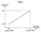
- FIG. 4is a graph representing a characteristic of a voltage controlled oscillator in the frequency synthesizer circuit according to the first embodiment of the present invention
- FIG. 5is a detailed block diagram of a control circuit in the frequency synthesizer circuit according to the first embodiment of the present invention.
- FIG. 6is a logical diagram (truth table) of a control circuit in the frequency synthesizer circuit according to the first embodiment of the present invention.
- FIG. 7is a detailed block diagram of a PLL circuit with a modification in the frequency synthesizer circuit according to the first embodiment of the present invention.
- FIG. 8is a detailed block diagram of a control circuit in a frequency synthesizer circuit according to a second embodiment of the present invention.
- FIG. 9is a graph representing a characteristic of a voltage controlled oscillator in the frequency synthesizer circuit according to the second embodiment of the present invention.
- FIG. 10is a logical diagram (truth table) of a control circuit in the frequency synthesizer circuit according to the second embodiment of the present invention.
- FIG. 11is an overall schematic block diagram of a frequency synthesizer circuit according to another embodiment of the present invention.
- FIG. 2is an overall schematic block diagram of the frequency synthesizer circuit according to the first embodiment
- FIG. 3is a detailed block diagram of a PLL circuit in the frequency synthesizer circuit according to the first embodiment
- FIG. 4is a graph representing a characteristic of a voltage controlled oscillator in the frequency synthesizer circuit according to the first embodiment
- FIG. 5is a detailed block diagram of a control diagram in the frequency synthesizer circuit according to the first embodiment
- FIG. 6is a logical diagram (truth table) of the control circuit in the frequency synthesizer circuit according to the first embodiment.
- the frequency synthesizer circuit 10comprises a PLL circuit 1 , a voltage controlled oscillator (VCO) 2 connected to the PLL circuit 1 , a low pass filter (LPF) 3 connected to the PLL circuit 1 , and a control circuit 4 , which is characteristic of the present invention.
- the PLL circuit 1includes a phase comparator 11 that generates a phase difference signal based on a phase difference between an oscillation signal provided from the VCO 2 and a reference signal provided from a reference signal source REF, a first counter 12 , a shift register 13 , a second counter 15 , and a charge pump 16 .
- the VCO 2changes a value of the oscillation signal depending on control voltage received from the control circuit 4 .
- the LPF 3blocks a high frequency component of the phase difference signal provided from the PLL circuit 1 .
- the control circuit 4is connected to the PLL circuit in order to receive either 2 control bits (a control bit A and a control bit B) as a control signal or the phase difference signal having its high frequency component removed from the LPF 3 .
- the control circuit 4provides the control voltage to the VCO 2 with a different value based on the control signal or the phase difference signal.
- the PLL circuit 1 , the VCO 2 , the LPF 3 , and the control circuit 4are all mounted on a single chip. Also shown in FIG.
- Probes 20 a , 20 b of the testing device 20are connected to a terminal 1 a and a terminal 2 b , respectively, which are formed on the frequency synthesizer circuit 10 according to the first embodiment of the present invention.
- the phase comparator 11receives the oscillation signal from the VCO 2 via the first counter 12 and the reference signal from the reference signal source via the second counter 15 . The phase comparator 11 then detects the phase difference between them. The detected phase difference is provided from the phase comparator 11 to the LPF 3 as the phase difference signal in the form of a pulse.
- the shift register 13 in the PLL circuit 1generates the control bit A and the control bit B to be provided to the control circuit 4 based on the control signal included in serial data provided from the testing device 20 .
- the VCO 2receives the phase difference signal provided from the PLL circuit 1 via the LPF 3 as the control voltage and generates the oscillation signal based on the control voltage in accordance with the characteristic of the VCO 2 as shown in FIG. 4 .
- the control circuit 4serves as a testing unit and provides the control voltage with a different value to the VCO 2 based on the control bits provided from the PLL circuit 1 or the phase difference signal provided from the PLL circuit 1 via the LPF 3 .
- the control circuit 4provides the control voltage determined from the phase difference signal provided from the PLL circuit 1 via the LPF 3 as mentioned above.
- the control circuit 4is switched to a testing operation mode and the control circuit 4 provides the control voltage having either the upper limit value or the lower limit value to the VCO 2 .
- the control circuit 4comprises a first switch 41 and a second switch 42 .
- the first switch 41connects the VCO 2 to either the LPF 3 or the second switch 42 .
- the VCO 2is switched between the LPF 3 and the second switch 42 .
- the second switch 42connects the first switch 41 to either a voltage source ⁇ generating voltage of the upper limit value of the control voltage (2.5 V) or a voltage source ⁇ generating the voltage of the lower limit value of the control voltage (0.5 V).
- the first switch 41is switched between the voltage source ⁇ and the voltage source ⁇ . Therefore, the control circuit 4 switches the first switch 41 and the second switch 42 depending on the control bits provided from the PLL circuit 1 . More particularly, as shown in FIG.
- the control circuit 4provides the control voltage having the lower limit value to the VCO 2 when the value of both the control bits A, B is 0.
- the control circuit 4provides the control voltage having the upper limit value to the VCO 2 when the value of the control bit A is 0 and the value of the control bit B is 1.
- the above two casesindicate that the control circuit 4 is in the testing operation mode.
- the control circuit 4provides the control voltage determined from the phase difference signal provided from the PLL circuit 1 in the cases other than those mentioned above. This indicates that the control circuit 4 is in the normal operation mode.
- control circuit 4is not limited to that mentioned above.
- the serial data that determines the control bits A, Bis provided to the PLL circuit 1 via the terminal 1 a of the frequency synthesizer circuit 10 according to the first embodiment when a probe of the testing device 20 is connected to the terminal 1 a at the time of the wafer probing test.
- the followingis a description of operations of the frequency synthesizer circuit 10 according to the first embodiment of the present invention.
- the descriptionwill be given to the normal operation mode and the testing operation mode.
- a default value of both the control bits A, B provided from the PLL circuit 1 to the control circuit 4is set to 1.
- the control bits A, Beach maintains the value of 1 unless the serial data is provided from the testing device 20 , is provided to the PLL circuit 1 .
- the VCO 2provides the oscillation signal having an oscillation frequency corresponding to the default values of the control bits A, B to the exterior as well as to the PLL circuit 1 via a branch.
- the PLL circuit 1detects the phase difference between the reference signal from the reference signal source REF and the oscillation signal from the VCO 2 , and provides the phase difference as the phase difference signal in the form of a pulse to the LPF 3 , which is connected to the PLL circuit 1 .
- the LPF 3blocks the high frequency component of the phase difference signal received from the PLL circuit 1 and provides the phase difference signal having its high frequency component removed to the control circuit 4 .
- the first switch 41Since the value of each of the control bits A, B received from the PLL circuit 1 is 1, the first switch 41 switches so as to connect the LPF 3 to the VCO 2 . Therefore, the control voltage determined from the phase difference signal provided from the PLL circuit 1 via the LPF 3 is provided to the VCO 2 . The VCO 2 generates the oscillation signal based on the phase difference signal received as the control voltage.
- the normal operation modeis performed when the value of the control bit A is 1 and the value of the control bit B is 0. In such a case, as mentioned above, the first switch 41 switches so as to connect the LPF 3 to the VCO 2 and thus the control voltage determined from the phase difference signal provided from the PLL circuit 1 via the LPF 3 is provided to the VCO 2 . The normal operation mode is continued as long as the value of the control bit A is not changed.
- the serial data that determines the control bits A, Bis provided from the testing device 20 through the PLL circuit 1 .
- the followingis a description of a case when each of the value of the control bits A, B is changed to 0, from the default value of 1.
- the control circuit 4switches the first switch 41 so as to connect the VCO 2 to the second switch 42 .
- the control circuit 4also switches the second switch 42 so as to connect the first switch 41 to the voltage source ⁇ . Accordingly, the control voltage having the lower limit value (0.5 V) is provided to the VCO 2 .
- the VCO 2generates the oscillation signal having a predetermined frequency oscillation according to the control voltage with the lower limit value, it can be determined that the VCO 2 is working properly. If the VCO 2 cannot generate the oscillation signal having the predetermined frequency oscillation according to the control voltage with the lower limit value, it can be determined that the VCO 2 has a failure.
- control bit Amay be maintained the same, i.e. 0, and the value of the control bit B may be changed to 1 from the value of 0 when the serial data that determines the control bits A, B is provided from the testing device 20 .
- the control circuit 4switches the switch 41 so as to connect the VCO 2 to the second switch 42 .
- the control circuit 4also switches the second switch 42 so as to connect the first switch 41 to the voltage source ⁇ .
- the control voltage having the upper limit value(2.5 V) is provided to the VCO 2 .
- the VCO 2generates the oscillation signal having a predetermined frequency oscillation according to the control voltage with the upper limit value, it can be determined that the VCO 2 is working properly. If the VCO 2 cannot generate the oscillation signal having a predetermined frequency oscillation according to the control voltage with the upper limit value, it can be determined that the VCO 2 has a failure.
- the control circuit 4is in the normal operation mode when the value of the control bit A is 1 and thus the first switch 41 connects the LPF 3 to the VCO 2 . Therefore, the phase difference signal provided from the PLL circuit 1 is provided to the VCO 2 via the LPF 3 as the control voltage and the VCO 2 generates the oscillation signal having the predetermined oscillation frequency in accordance with the phase difference signal.
- the control circuit 4is in the testing operation mode, in which the wafer probing test is to be performed to check the oscillation frequency provided from the VCO 2 , when the values of the control bits A, B are changed from the default values.
- control voltage having either the upper limit value or the lower limit valueis provided to the VCO 2 so as to determine whether the VCO 2 can generate the oscillation signal having an appropriate oscillation frequency according to the control voltage. Therefore, the wafer-probing test can be easily performed before the assembly of the frequency synthesizer circuit into the final product.
- a selector 14may be further provided in the PLL circuit 1 so as to receive the reference signal provided from the reference signal source REF and the oscillation signal provided from the VCO 2 as similar to the phase comparator 11 .
- the wafer-probing testcan also be performed by switching the selector 14 so as to provide either the reference signal or the oscillation signal. Normally, when the oscillation frequency of the oscillation signal exceeds several giga hertz, the direct reading out of the oscillation signal provided from the VCO 2 by the probe of the testing device 20 may present a problem since the frequency band is high.
- the probe of the testing device 20can read out the oscillation signal with an admissible frequency band. Therefore, the wafer-probing test can be easily performed.
- FIG. 8is a detailed block diagram of a control circuit in the frequency synthesizer circuit according to the second embodiment.
- the frequency synthesizer circuit according to the second embodimentis configured similarly to the frequency synthesizer circuit according to the first embodiment.
- the second embodimentis configured so as to use 3 control bits A, B, and C as compared to 2 control bits A, B in the first embodiment.
- the control circuit 4includes, in addition to the configuration of the first embodiment shown in FIG. 5, a NOT gate element 43 , an AND gate element 44 receiving the control bit A from the PLL circuit 1 via the NOT gate element 43 and the control bit C from the PLL circuit 1 , and a selector 45 receiving a control bit provided from the AND gate element 44 .
- the selector 45provides channel selection signals s 1 , s 2 according to the control bit provided from the AND gate element 44 .
- the VCO 2 in the second embodimentprovides the oscillation signal according to either the frequency bands ch 1 (2.05-2.43 GHz) or the frequency band ch 2 (2.43-2.75 GHz), which is higher than the frequency band ch 1 as shown in FIG. 9 .
- the VCO 2generates the oscillation signal according to either the oscillation frequency band ch 1 or the oscillation frequency band ch 2 depending on the channel selection signals s 1 , s 2 provided from the selector 45 . As shown in FIG.
- the control circuit 4when the value of each of the control bits A, C is 0, regardless of the value of the control bit B, the control circuit 4 provides the channel selection signal s 1 to the VCO 2 so that the VCO 2 provides the oscillation signal according to the oscillation frequency band ch 1 . Also, when the value of the control bit A is 0 and the value of the control bit C is 1, regardless of the value of the control bit B, the control circuit 4 provides the channel selection signal s 2 to the VCO 2 so that the VCO 2 provides the oscillation signal according to the oscillation frequency band ch 2 .
- the frequency synthesizer circuit according to the second embodimentoperates similarly to the first embodiment of the present invention.
- the frequency synthesizer circuit according to the second embodimentoperates as described below.
- the channel selection signal s 1is provided to the VCO 2 so that the VCO 2 provides the oscillation signal having the oscillation frequency corresponding to the lower limit of the lowest frequency band ch 1 , i.e. 2.05 GHz.
- the channel selection signal s 1is provided to the VCO 2 so that the VCO 2 provides the oscillation signal having the oscillation frequency corresponding to the upper limit of the lowest frequency band ch 1 , i.e. 2.43 GHz.
- the channel selection signal s 2is provided to the VCO 2 so that the VCO 2 provides the oscillation signal having the oscillation frequency corresponding to the lower limit of the highest frequency band ch 2 , i.e. 2.43 GHz.
- the channel selection signal s 2is provided to the VCO 2 so that the VCO 2 provides the oscillation signal having the oscillation frequency corresponding to the upper limit of the highest frequency band ch 1 , i.e. 2.75 GHz.
- the control circuit 4is in the normal operation mode, during which the oscillation signal with the predetermined oscillation frequency according to the phase difference detected in the PLL circuit 1 is provided from the VCO 2 .
- the VCO 2may be provided with 2 oscillation frequency bands.
- the additional use of the control bit C in addition to the control bits A, B, which are used in the frequency synthesizer according to the first embodiment,allows performing the wafer-probing test so as to check the oscillation frequency provided from such a VCO 2 .
- the values of the control bit A, the control bit B, and the control bit Care changed accordingly so as to provide the oscillation signal with the oscillation frequency corresponding to the lower limit of the lowest frequency band, the oscillation signal with the oscillation frequency corresponding to the upper limit of the lowest frequency band ch 1 , the oscillation signal with the oscillation frequency corresponding to the lower limit of the highest frequency band ch 2 , and the oscillation signal with the oscillation frequency corresponding to the upper limit of the highest frequency band ch 2 . It is possible to determine if the VCO 2 is working properly or not by determining whether the VCO 2 is providing the oscillation signal with the appropriate oscillation frequency according to the different frequency band based on the control voltage provided from the control circuit 4 . Thus the wafer-probing test can be easily performed before the assembly of the frequency synthesizer circuit.
- frequency synthesizer circuitaccording to the second embodiment, more than 2 frequency bands may be employed by increasing the number of control bits to be used.
- FIG. 11shows a frequency synthesizer circuit according to another embodiment of the present invention.
- the frequency synthesizer circuit according to another embodimentis configured similarly to the frequency synthesizer according to the first embodiment, however, the LPF 3 may be constructed as a passive filter and the control circuit 4 may be located in the PLL circuit 1 instead of between the VCO 2 and the LPF 3 as in the frequency synthesizer according to the first embodiment. Therefore, the control voltage may be provided to the VCO 2 via the passive filter, which is configuring the LPF 3 , without directly connecting the control circuit 4 to the VCO 2 .
Landscapes
- Stabilization Of Oscillater, Synchronisation, Frequency Synthesizers (AREA)
Abstract
Description
Claims (8)
Applications Claiming Priority (2)
| Application Number | Priority Date | Filing Date | Title |
|---|---|---|---|
| JP2002145304AJP4029138B2 (en) | 2002-05-20 | 2002-05-20 | Frequency synthesizer circuit |
| JP2002-145304 | 2002-05-20 |
Publications (2)
| Publication Number | Publication Date |
|---|---|
| US20030214360A1 US20030214360A1 (en) | 2003-11-20 |
| US6806782B2true US6806782B2 (en) | 2004-10-19 |
Family
ID=29417110
Family Applications (1)
| Application Number | Title | Priority Date | Filing Date |
|---|---|---|---|
| US10/419,206Expired - LifetimeUS6806782B2 (en) | 2002-05-20 | 2003-04-21 | Frequency synthesizer circuit |
Country Status (4)
| Country | Link |
|---|---|
| US (1) | US6806782B2 (en) |
| JP (1) | JP4029138B2 (en) |
| KR (1) | KR100891475B1 (en) |
| CN (1) | CN1225840C (en) |
Cited By (38)
| Publication number | Priority date | Publication date | Assignee | Title |
|---|---|---|---|---|
| US7737724B2 (en) | 2007-04-17 | 2010-06-15 | Cypress Semiconductor Corporation | Universal digital block interconnection and channel routing |
| US7761845B1 (en) | 2002-09-09 | 2010-07-20 | Cypress Semiconductor Corporation | Method for parameterizing a user module |
| US7765095B1 (en) | 2000-10-26 | 2010-07-27 | Cypress Semiconductor Corporation | Conditional branching in an in-circuit emulation system |
| US7770113B1 (en) | 2001-11-19 | 2010-08-03 | Cypress Semiconductor Corporation | System and method for dynamically generating a configuration datasheet |
| US7774190B1 (en) | 2001-11-19 | 2010-08-10 | Cypress Semiconductor Corporation | Sleep and stall in an in-circuit emulation system |
| US7825688B1 (en) | 2000-10-26 | 2010-11-02 | Cypress Semiconductor Corporation | Programmable microcontroller architecture(mixed analog/digital) |
| US7844437B1 (en) | 2001-11-19 | 2010-11-30 | Cypress Semiconductor Corporation | System and method for performing next placements and pruning of disallowed placements for programming an integrated circuit |
| US7893724B2 (en) | 2004-03-25 | 2011-02-22 | Cypress Semiconductor Corporation | Method and circuit for rapid alignment of signals |
| US8026739B2 (en) | 2007-04-17 | 2011-09-27 | Cypress Semiconductor Corporation | System level interconnect with programmable switching |
| US8040266B2 (en) | 2007-04-17 | 2011-10-18 | Cypress Semiconductor Corporation | Programmable sigma-delta analog-to-digital converter |
| US8049569B1 (en) | 2007-09-05 | 2011-11-01 | Cypress Semiconductor Corporation | Circuit and method for improving the accuracy of a crystal-less oscillator having dual-frequency modes |
| US8067948B2 (en) | 2006-03-27 | 2011-11-29 | Cypress Semiconductor Corporation | Input/output multiplexer bus |
| US8069436B2 (en) | 2004-08-13 | 2011-11-29 | Cypress Semiconductor Corporation | Providing hardware independence to automate code generation of processing device firmware |
| US8069405B1 (en) | 2001-11-19 | 2011-11-29 | Cypress Semiconductor Corporation | User interface for efficiently browsing an electronic document using data-driven tabs |
| US8069428B1 (en) | 2001-10-24 | 2011-11-29 | Cypress Semiconductor Corporation | Techniques for generating microcontroller configuration information |
| US8078894B1 (en) | 2007-04-25 | 2011-12-13 | Cypress Semiconductor Corporation | Power management architecture, method and configuration system |
| US8078970B1 (en) | 2001-11-09 | 2011-12-13 | Cypress Semiconductor Corporation | Graphical user interface with user-selectable list-box |
| US8085100B2 (en) | 2005-02-04 | 2011-12-27 | Cypress Semiconductor Corporation | Poly-phase frequency synthesis oscillator |
| US8085067B1 (en) | 2005-12-21 | 2011-12-27 | Cypress Semiconductor Corporation | Differential-to-single ended signal converter circuit and method |
| US8089461B2 (en) | 2005-06-23 | 2012-01-03 | Cypress Semiconductor Corporation | Touch wake for electronic devices |
| US8092083B2 (en) | 2007-04-17 | 2012-01-10 | Cypress Semiconductor Corporation | Temperature sensor with digital bandgap |
| US8103497B1 (en) | 2002-03-28 | 2012-01-24 | Cypress Semiconductor Corporation | External interface for event architecture |
| US8103496B1 (en) | 2000-10-26 | 2012-01-24 | Cypress Semicondutor Corporation | Breakpoint control in an in-circuit emulation system |
| US8120408B1 (en) | 2005-05-05 | 2012-02-21 | Cypress Semiconductor Corporation | Voltage controlled oscillator delay cell and method |
| US8132039B1 (en)* | 2007-10-31 | 2012-03-06 | Altera Corporation | Techniques for generating clock signals using counters |
| US8130025B2 (en) | 2007-04-17 | 2012-03-06 | Cypress Semiconductor Corporation | Numerical band gap |
| US8149048B1 (en) | 2000-10-26 | 2012-04-03 | Cypress Semiconductor Corporation | Apparatus and method for programmable power management in a programmable analog circuit block |
| US8160864B1 (en) | 2000-10-26 | 2012-04-17 | Cypress Semiconductor Corporation | In-circuit emulator and pod synchronized boot |
| US8176296B2 (en) | 2000-10-26 | 2012-05-08 | Cypress Semiconductor Corporation | Programmable microcontroller architecture |
| US8286125B2 (en) | 2004-08-13 | 2012-10-09 | Cypress Semiconductor Corporation | Model for a hardware device-independent method of defining embedded firmware for programmable systems |
| US8402313B1 (en) | 2002-05-01 | 2013-03-19 | Cypress Semiconductor Corporation | Reconfigurable testing system and method |
| US8499270B1 (en) | 2007-04-25 | 2013-07-30 | Cypress Semiconductor Corporation | Configuration of programmable IC design elements |
| US8516025B2 (en) | 2007-04-17 | 2013-08-20 | Cypress Semiconductor Corporation | Clock driven dynamic datapath chaining |
| US8533677B1 (en) | 2001-11-19 | 2013-09-10 | Cypress Semiconductor Corporation | Graphical user interface for dynamically reconfiguring a programmable device |
| US9448964B2 (en) | 2009-05-04 | 2016-09-20 | Cypress Semiconductor Corporation | Autonomous control in a programmable system |
| US9564902B2 (en) | 2007-04-17 | 2017-02-07 | Cypress Semiconductor Corporation | Dynamically configurable and re-configurable data path |
| US9720805B1 (en) | 2007-04-25 | 2017-08-01 | Cypress Semiconductor Corporation | System and method for controlling a target device |
| US10698662B2 (en) | 2001-11-15 | 2020-06-30 | Cypress Semiconductor Corporation | System providing automatic source code generation for personalization and parameterization of user modules |
Families Citing this family (5)
| Publication number | Priority date | Publication date | Assignee | Title |
|---|---|---|---|---|
| US7265633B1 (en)* | 2004-06-14 | 2007-09-04 | Cypress Semiconductor Corporation | Open loop bandwidth test architecture and method for phase locked loop (PLL) |
| JP2008531248A (en)* | 2005-02-16 | 2008-08-14 | スリーエム イノベイティブ プロパティズ カンパニー | Method for producing topographically patterned coatings |
| US8143958B2 (en)* | 2009-05-20 | 2012-03-27 | Qualcomm, Incorporated | Systems and methods for self testing a voltage controlled oscillator in an open loop configuration |
| WO2013145020A1 (en)* | 2012-03-30 | 2013-10-03 | 株式会社日立製作所 | Time domain spectroscopic device and time domain spectroscopic analysis system |
| CN111884652A (en)* | 2020-08-26 | 2020-11-03 | 天津七一二通信广播股份有限公司 | Phase-locked loop circuit with function of quickly locking frequency |
Citations (2)
| Publication number | Priority date | Publication date | Assignee | Title |
|---|---|---|---|---|
| JPH0795069A (en) | 1993-09-20 | 1995-04-07 | Fujitsu Ltd | PLL synthesizer with high-speed lockup control |
| US5942949A (en)* | 1997-10-14 | 1999-08-24 | Lucent Technologies Inc. | Self-calibrating phase-lock loop with auto-trim operations for selecting an appropriate oscillator operating curve |
Family Cites Families (4)
| Publication number | Priority date | Publication date | Assignee | Title |
|---|---|---|---|---|
| JP2581398B2 (en) | 1993-07-12 | 1997-02-12 | 日本電気株式会社 | PLL frequency synthesizer |
| JP2875472B2 (en) | 1994-01-19 | 1999-03-31 | 日本無線株式会社 | PLL synthesizer and control method thereof |
| KR20000007762A (en)* | 1998-07-07 | 2000-02-07 | 이형도 | Open loop type phase synchronizing loop synthesizer |
| JP2000252819A (en)* | 1999-03-01 | 2000-09-14 | Toshiba Corp | PLL circuit |
- 2002
- 2002-05-20JPJP2002145304Apatent/JP4029138B2/ennot_activeExpired - Fee Related
- 2003
- 2003-04-21USUS10/419,206patent/US6806782B2/ennot_activeExpired - Lifetime
- 2003-05-15KRKR1020030030791Apatent/KR100891475B1/ennot_activeExpired - Fee Related
- 2003-05-20CNCNB031368352Apatent/CN1225840C/ennot_activeExpired - Fee Related
Patent Citations (2)
| Publication number | Priority date | Publication date | Assignee | Title |
|---|---|---|---|---|
| JPH0795069A (en) | 1993-09-20 | 1995-04-07 | Fujitsu Ltd | PLL synthesizer with high-speed lockup control |
| US5942949A (en)* | 1997-10-14 | 1999-08-24 | Lucent Technologies Inc. | Self-calibrating phase-lock loop with auto-trim operations for selecting an appropriate oscillator operating curve |
Cited By (53)
| Publication number | Priority date | Publication date | Assignee | Title |
|---|---|---|---|---|
| US8103496B1 (en) | 2000-10-26 | 2012-01-24 | Cypress Semicondutor Corporation | Breakpoint control in an in-circuit emulation system |
| US10725954B2 (en) | 2000-10-26 | 2020-07-28 | Monterey Research, Llc | Microcontroller programmable system on a chip |
| US7765095B1 (en) | 2000-10-26 | 2010-07-27 | Cypress Semiconductor Corporation | Conditional branching in an in-circuit emulation system |
| US10261932B2 (en) | 2000-10-26 | 2019-04-16 | Cypress Semiconductor Corporation | Microcontroller programmable system on a chip |
| US10248604B2 (en) | 2000-10-26 | 2019-04-02 | Cypress Semiconductor Corporation | Microcontroller programmable system on a chip |
| US7825688B1 (en) | 2000-10-26 | 2010-11-02 | Cypress Semiconductor Corporation | Programmable microcontroller architecture(mixed analog/digital) |
| US10020810B2 (en) | 2000-10-26 | 2018-07-10 | Cypress Semiconductor Corporation | PSoC architecture |
| US9843327B1 (en) | 2000-10-26 | 2017-12-12 | Cypress Semiconductor Corporation | PSOC architecture |
| US9766650B2 (en) | 2000-10-26 | 2017-09-19 | Cypress Semiconductor Corporation | Microcontroller programmable system on a chip with programmable interconnect |
| US8736303B2 (en) | 2000-10-26 | 2014-05-27 | Cypress Semiconductor Corporation | PSOC architecture |
| US8555032B2 (en) | 2000-10-26 | 2013-10-08 | Cypress Semiconductor Corporation | Microcontroller programmable system on a chip with programmable interconnect |
| US8358150B1 (en) | 2000-10-26 | 2013-01-22 | Cypress Semiconductor Corporation | Programmable microcontroller architecture(mixed analog/digital) |
| US8176296B2 (en) | 2000-10-26 | 2012-05-08 | Cypress Semiconductor Corporation | Programmable microcontroller architecture |
| US8160864B1 (en) | 2000-10-26 | 2012-04-17 | Cypress Semiconductor Corporation | In-circuit emulator and pod synchronized boot |
| US8149048B1 (en) | 2000-10-26 | 2012-04-03 | Cypress Semiconductor Corporation | Apparatus and method for programmable power management in a programmable analog circuit block |
| US8793635B1 (en) | 2001-10-24 | 2014-07-29 | Cypress Semiconductor Corporation | Techniques for generating microcontroller configuration information |
| US8069428B1 (en) | 2001-10-24 | 2011-11-29 | Cypress Semiconductor Corporation | Techniques for generating microcontroller configuration information |
| US10466980B2 (en) | 2001-10-24 | 2019-11-05 | Cypress Semiconductor Corporation | Techniques for generating microcontroller configuration information |
| US8078970B1 (en) | 2001-11-09 | 2011-12-13 | Cypress Semiconductor Corporation | Graphical user interface with user-selectable list-box |
| US10698662B2 (en) | 2001-11-15 | 2020-06-30 | Cypress Semiconductor Corporation | System providing automatic source code generation for personalization and parameterization of user modules |
| US8370791B2 (en) | 2001-11-19 | 2013-02-05 | Cypress Semiconductor Corporation | System and method for performing next placements and pruning of disallowed placements for programming an integrated circuit |
| US7774190B1 (en) | 2001-11-19 | 2010-08-10 | Cypress Semiconductor Corporation | Sleep and stall in an in-circuit emulation system |
| US8533677B1 (en) | 2001-11-19 | 2013-09-10 | Cypress Semiconductor Corporation | Graphical user interface for dynamically reconfiguring a programmable device |
| US7844437B1 (en) | 2001-11-19 | 2010-11-30 | Cypress Semiconductor Corporation | System and method for performing next placements and pruning of disallowed placements for programming an integrated circuit |
| US8069405B1 (en) | 2001-11-19 | 2011-11-29 | Cypress Semiconductor Corporation | User interface for efficiently browsing an electronic document using data-driven tabs |
| US7770113B1 (en) | 2001-11-19 | 2010-08-03 | Cypress Semiconductor Corporation | System and method for dynamically generating a configuration datasheet |
| US8103497B1 (en) | 2002-03-28 | 2012-01-24 | Cypress Semiconductor Corporation | External interface for event architecture |
| US8402313B1 (en) | 2002-05-01 | 2013-03-19 | Cypress Semiconductor Corporation | Reconfigurable testing system and method |
| US7761845B1 (en) | 2002-09-09 | 2010-07-20 | Cypress Semiconductor Corporation | Method for parameterizing a user module |
| US7893724B2 (en) | 2004-03-25 | 2011-02-22 | Cypress Semiconductor Corporation | Method and circuit for rapid alignment of signals |
| US8069436B2 (en) | 2004-08-13 | 2011-11-29 | Cypress Semiconductor Corporation | Providing hardware independence to automate code generation of processing device firmware |
| US8286125B2 (en) | 2004-08-13 | 2012-10-09 | Cypress Semiconductor Corporation | Model for a hardware device-independent method of defining embedded firmware for programmable systems |
| US8085100B2 (en) | 2005-02-04 | 2011-12-27 | Cypress Semiconductor Corporation | Poly-phase frequency synthesis oscillator |
| US8120408B1 (en) | 2005-05-05 | 2012-02-21 | Cypress Semiconductor Corporation | Voltage controlled oscillator delay cell and method |
| US8089461B2 (en) | 2005-06-23 | 2012-01-03 | Cypress Semiconductor Corporation | Touch wake for electronic devices |
| US8085067B1 (en) | 2005-12-21 | 2011-12-27 | Cypress Semiconductor Corporation | Differential-to-single ended signal converter circuit and method |
| US8067948B2 (en) | 2006-03-27 | 2011-11-29 | Cypress Semiconductor Corporation | Input/output multiplexer bus |
| US8717042B1 (en) | 2006-03-27 | 2014-05-06 | Cypress Semiconductor Corporation | Input/output multiplexer bus |
| US9564902B2 (en) | 2007-04-17 | 2017-02-07 | Cypress Semiconductor Corporation | Dynamically configurable and re-configurable data path |
| US8476928B1 (en) | 2007-04-17 | 2013-07-02 | Cypress Semiconductor Corporation | System level interconnect with programmable switching |
| US7737724B2 (en) | 2007-04-17 | 2010-06-15 | Cypress Semiconductor Corporation | Universal digital block interconnection and channel routing |
| US8092083B2 (en) | 2007-04-17 | 2012-01-10 | Cypress Semiconductor Corporation | Temperature sensor with digital bandgap |
| US8130025B2 (en) | 2007-04-17 | 2012-03-06 | Cypress Semiconductor Corporation | Numerical band gap |
| US8040266B2 (en) | 2007-04-17 | 2011-10-18 | Cypress Semiconductor Corporation | Programmable sigma-delta analog-to-digital converter |
| US8516025B2 (en) | 2007-04-17 | 2013-08-20 | Cypress Semiconductor Corporation | Clock driven dynamic datapath chaining |
| US8026739B2 (en) | 2007-04-17 | 2011-09-27 | Cypress Semiconductor Corporation | System level interconnect with programmable switching |
| US9720805B1 (en) | 2007-04-25 | 2017-08-01 | Cypress Semiconductor Corporation | System and method for controlling a target device |
| US8499270B1 (en) | 2007-04-25 | 2013-07-30 | Cypress Semiconductor Corporation | Configuration of programmable IC design elements |
| US8078894B1 (en) | 2007-04-25 | 2011-12-13 | Cypress Semiconductor Corporation | Power management architecture, method and configuration system |
| US8909960B1 (en) | 2007-04-25 | 2014-12-09 | Cypress Semiconductor Corporation | Power management architecture, method and configuration system |
| US8049569B1 (en) | 2007-09-05 | 2011-11-01 | Cypress Semiconductor Corporation | Circuit and method for improving the accuracy of a crystal-less oscillator having dual-frequency modes |
| US8132039B1 (en)* | 2007-10-31 | 2012-03-06 | Altera Corporation | Techniques for generating clock signals using counters |
| US9448964B2 (en) | 2009-05-04 | 2016-09-20 | Cypress Semiconductor Corporation | Autonomous control in a programmable system |
Also Published As
| Publication number | Publication date |
|---|---|
| JP2003338752A (en) | 2003-11-28 |
| KR20030090510A (en) | 2003-11-28 |
| US20030214360A1 (en) | 2003-11-20 |
| JP4029138B2 (en) | 2008-01-09 |
| CN1461111A (en) | 2003-12-10 |
| KR100891475B1 (en) | 2009-04-02 |
| CN1225840C (en) | 2005-11-02 |
Similar Documents
| Publication | Publication Date | Title |
|---|---|---|
| US6806782B2 (en) | Frequency synthesizer circuit | |
| US6859028B2 (en) | Design-for-test modes for a phase locked loop | |
| KR0139136B1 (en) | Clock signal generation circuit capable of operating at high speed with high frequency | |
| US7522690B2 (en) | Jitter self test | |
| US6216254B1 (en) | Integrated circuit design using a frequency synthesizer that automatically ensures testability | |
| US7328383B2 (en) | Circuit and method for testing embedded phase-locked loop circuit | |
| US5381087A (en) | LSI with built-in test circuit and testing method therefor | |
| US20050237119A1 (en) | Frequency synthesizer, radio communication system using the synthesizer, and control method of the synthesizer | |
| US7023195B2 (en) | Module, system and method for testing a phase locked loop | |
| US6597162B2 (en) | PLL semiconductor device with testability, and method and apparatus for testing same | |
| US6316929B1 (en) | Frequency measurement test circuit and semiconductor integrated circuit having the same | |
| US7705581B2 (en) | Electronic device and method for on chip jitter measurement | |
| US7555686B2 (en) | Semiconductor device, test board for testing the same, and test system and method for testing the same | |
| US20010006343A1 (en) | Integrated circuit and lot selection system therefor | |
| US20030132775A1 (en) | Test apparatus for an oscillation circuit incorporated in IC | |
| US6952373B2 (en) | Semiconductor device having PLL-circuit | |
| JP3647699B2 (en) | Integrated circuit and lot sorting system | |
| US6777921B2 (en) | Analog filter with built-in self test | |
| US6674301B2 (en) | Method and system of evaluating PLL built-in circuit | |
| Sekyere et al. | Robust Defect Detection for Phase-Locked Loops using All-Digital Built-In Self-Test (BIST) Circuitry | |
| JP2001091595A (en) | LSI semiconductor inspection device and semiconductor device | |
| WO2008152082A1 (en) | Electronic device and method for on chip jitter measurement | |
| KR20050050453A (en) | Divider resister and resister check method |
Legal Events
| Date | Code | Title | Description |
|---|---|---|---|
| AS | Assignment | Owner name:FUJITSU LIMITED, JAPAN Free format text:ASSIGNMENT OF ASSIGNORS INTEREST;ASSIGNORS:MOTOYOSHI, TOSHIRO;NAGATA, KIMIHIKO;REEL/FRAME:013989/0838 Effective date:20030402 | |
| STCF | Information on status: patent grant | Free format text:PATENTED CASE | |
| FEPP | Fee payment procedure | Free format text:PAYOR NUMBER ASSIGNED (ORIGINAL EVENT CODE: ASPN); ENTITY STATUS OF PATENT OWNER: LARGE ENTITY | |
| CC | Certificate of correction | ||
| FPAY | Fee payment | Year of fee payment:4 | |
| AS | Assignment | Owner name:FUJITSU MICROELECTRONICS LIMITED, JAPAN Free format text:ASSIGNMENT OF ASSIGNORS INTEREST;ASSIGNOR:FUJITSU LIMITED;REEL/FRAME:021998/0645 Effective date:20081104 Owner name:FUJITSU MICROELECTRONICS LIMITED,JAPAN Free format text:ASSIGNMENT OF ASSIGNORS INTEREST;ASSIGNOR:FUJITSU LIMITED;REEL/FRAME:021998/0645 Effective date:20081104 | |
| AS | Assignment | Owner name:FUJITSU SEMICONDUCTOR LIMITED, JAPAN Free format text:CHANGE OF NAME;ASSIGNOR:FUJITSU MICROELECTRONICS LIMITED;REEL/FRAME:024982/0245 Effective date:20100401 | |
| FPAY | Fee payment | Year of fee payment:8 | |
| AS | Assignment | Owner name:SPANSION LLC, CALIFORNIA Free format text:ASSIGNMENT OF ASSIGNORS INTEREST;ASSIGNOR:FUJITSU SEMICONDUCTOR LIMITED;REEL/FRAME:031205/0461 Effective date:20130829 | |
| AS | Assignment | Owner name:MORGAN STANLEY SENIOR FUNDING, INC., NEW YORK Free format text:SECURITY INTEREST;ASSIGNORS:CYPRESS SEMICONDUCTOR CORPORATION;SPANSION LLC;REEL/FRAME:035240/0429 Effective date:20150312 | |
| AS | Assignment | Owner name:CYPRESS SEMICONDUCTOR CORPORATION, CALIFORNIA Free format text:ASSIGNMENT OF ASSIGNORS INTEREST;ASSIGNOR:SPANSION, LLC;REEL/FRAME:036036/0490 Effective date:20150601 | |
| FPAY | Fee payment | Year of fee payment:12 | |
| AS | Assignment | Owner name:SPANSION LLC, CALIFORNIA Free format text:PARTIAL RELEASE OF SECURITY INTEREST IN PATENTS;ASSIGNOR:MORGAN STANLEY SENIOR FUNDING, INC., AS COLLATERAL AGENT;REEL/FRAME:039708/0001 Effective date:20160811 Owner name:CYPRESS SEMICONDUCTOR CORPORATION, CALIFORNIA Free format text:PARTIAL RELEASE OF SECURITY INTEREST IN PATENTS;ASSIGNOR:MORGAN STANLEY SENIOR FUNDING, INC., AS COLLATERAL AGENT;REEL/FRAME:039708/0001 Effective date:20160811 | |
| AS | Assignment | Owner name:MONTEREY RESEARCH, LLC, CALIFORNIA Free format text:ASSIGNMENT OF ASSIGNORS INTEREST;ASSIGNOR:CYPRESS SEMICONDUCTOR CORPORATION;REEL/FRAME:040911/0238 Effective date:20160811 | |
| AS | Assignment | Owner name:MORGAN STANLEY SENIOR FUNDING, INC., NEW YORK Free format text:CORRECTIVE ASSIGNMENT TO CORRECT THE 8647899 PREVIOUSLY RECORDED ON REEL 035240 FRAME 0429. ASSIGNOR(S) HEREBY CONFIRMS THE SECURITY INTERST;ASSIGNORS:CYPRESS SEMICONDUCTOR CORPORATION;SPANSION LLC;REEL/FRAME:058002/0470 Effective date:20150312 |