US6806186B2 - Submicron metallization using electrochemical deposition - Google Patents
Submicron metallization using electrochemical depositionDownload PDFInfo
- Publication number
- US6806186B2 US6806186B2US09/815,931US81593101AUS6806186B2US 6806186 B2US6806186 B2US 6806186B2US 81593101 AUS81593101 AUS 81593101AUS 6806186 B2US6806186 B2US 6806186B2
- Authority
- US
- United States
- Prior art keywords
- current density
- metal
- micro
- recessed structure
- electroplating
- Prior art date
- Legal status (The legal status is an assumption and is not a legal conclusion. Google has not performed a legal analysis and makes no representation as to the accuracy of the status listed.)
- Expired - Fee Related
Links
- 238000001465metallisationMethods0.000titleclaimsdescription29
- 238000004070electrodepositionMethods0.000titledescription3
- 238000000034methodMethods0.000claimsabstractdescription56
- 238000009713electroplatingMethods0.000claimsabstractdescription47
- 238000007747platingMethods0.000claimsabstractdescription45
- 229910052751metalInorganic materials0.000claimsabstractdescription40
- 239000002184metalSubstances0.000claimsabstractdescription40
- 238000000151depositionMethods0.000claimsabstractdescription32
- 230000008021depositionEffects0.000claimsabstractdescription20
- 238000004377microelectronicMethods0.000claimsabstractdescription20
- 229910052802copperInorganic materials0.000claimsdescription62
- 239000010949copperSubstances0.000claimsdescription62
- RYGMFSIKBFXOCR-UHFFFAOYSA-NCopperChemical compound[Cu]RYGMFSIKBFXOCR-UHFFFAOYSA-N0.000claimsdescription61
- 239000000243solutionSubstances0.000claimsdescription31
- 230000008569processEffects0.000claimsdescription22
- 239000006259organic additiveSubstances0.000claimsdescription16
- 239000004065semiconductorSubstances0.000claimsdescription15
- 229910021645metal ionInorganic materials0.000claimsdescription6
- 238000012545processingMethods0.000claimsdescription3
- 239000008151electrolyte solutionSubstances0.000claims2
- 230000002708enhancing effectEffects0.000claims2
- XLYOFNOQVPJJNP-UHFFFAOYSA-NwaterSubstancesOXLYOFNOQVPJJNP-UHFFFAOYSA-N0.000claims2
- 239000000654additiveSubstances0.000abstractdescription16
- 230000000996additive effectEffects0.000abstractdescription7
- 239000000758substrateSubstances0.000description9
- 239000010408filmSubstances0.000description7
- 239000004020conductorSubstances0.000description6
- 230000001934delayEffects0.000description5
- 239000003989dielectric materialSubstances0.000description5
- 239000000463materialSubstances0.000description5
- 230000000694effectsEffects0.000description4
- 235000012431wafersNutrition0.000description4
- 229910000838Al alloyInorganic materials0.000description3
- VYPSYNLAJGMNEJ-UHFFFAOYSA-NSilicium dioxideChemical compoundO=[Si]=OVYPSYNLAJGMNEJ-UHFFFAOYSA-N0.000description3
- 238000002474experimental methodMethods0.000description3
- 229910052814silicon oxideInorganic materials0.000description3
- XUIMIQQOPSSXEZ-UHFFFAOYSA-NSiliconChemical compound[Si]XUIMIQQOPSSXEZ-UHFFFAOYSA-N0.000description2
- 230000002378acidificating effectEffects0.000description2
- 230000004888barrier functionEffects0.000description2
- 230000008901benefitEffects0.000description2
- 230000015572biosynthetic processEffects0.000description2
- 238000009792diffusion processMethods0.000description2
- 230000009977dual effectEffects0.000description2
- 230000006872improvementEffects0.000description2
- 230000007246mechanismEffects0.000description2
- 238000005457optimizationMethods0.000description2
- 238000000059patterningMethods0.000description2
- 229910052710siliconInorganic materials0.000description2
- 239000010703siliconSubstances0.000description2
- QPLDLSVMHZLSFG-UHFFFAOYSA-NCopper oxideChemical compound[Cu]=OQPLDLSVMHZLSFG-UHFFFAOYSA-N0.000description1
- 239000005751Copper oxideSubstances0.000description1
- 239000002253acidSubstances0.000description1
- 238000013459approachMethods0.000description1
- 239000007864aqueous solutionSubstances0.000description1
- QVGXLLKOCUKJST-UHFFFAOYSA-Natomic oxygenChemical compound[O]QVGXLLKOCUKJST-UHFFFAOYSA-N0.000description1
- 239000003990capacitorSubstances0.000description1
- 150000001879copperChemical class0.000description1
- 229910000431copper oxideInorganic materials0.000description1
- 230000003247decreasing effectEffects0.000description1
- 238000011161developmentMethods0.000description1
- 238000009826distributionMethods0.000description1
- 230000005684electric fieldEffects0.000description1
- 238000005516engineering processMethods0.000description1
- 238000005530etchingMethods0.000description1
- -1halide compoundsChemical class0.000description1
- 238000011031large-scale manufacturing processMethods0.000description1
- 238000004519manufacturing processMethods0.000description1
- 150000002739metalsChemical class0.000description1
- 239000000203mixtureSubstances0.000description1
- 229910052760oxygenInorganic materials0.000description1
- 239000001301oxygenSubstances0.000description1
- 238000001020plasma etchingMethods0.000description1
- 230000010287polarizationEffects0.000description1
- 238000005498polishingMethods0.000description1
- 238000011160researchMethods0.000description1
- 230000008054signal transmissionEffects0.000description1
- 239000010409thin filmSubstances0.000description1
- 230000007704transitionEffects0.000description1
- 239000011800void materialSubstances0.000description1
Images


Classifications
- H—ELECTRICITY
- H01—ELECTRIC ELEMENTS
- H01L—SEMICONDUCTOR DEVICES NOT COVERED BY CLASS H10
- H01L21/00—Processes or apparatus adapted for the manufacture or treatment of semiconductor or solid state devices or of parts thereof
- H01L21/02—Manufacture or treatment of semiconductor devices or of parts thereof
- H01L21/04—Manufacture or treatment of semiconductor devices or of parts thereof the devices having potential barriers, e.g. a PN junction, depletion layer or carrier concentration layer
- H01L21/18—Manufacture or treatment of semiconductor devices or of parts thereof the devices having potential barriers, e.g. a PN junction, depletion layer or carrier concentration layer the devices having semiconductor bodies comprising elements of Group IV of the Periodic Table or AIIIBV compounds with or without impurities, e.g. doping materials
- H01L21/28—Manufacture of electrodes on semiconductor bodies using processes or apparatus not provided for in groups H01L21/20 - H01L21/268
- H01L21/283—Deposition of conductive or insulating materials for electrodes conducting electric current
- H01L21/288—Deposition of conductive or insulating materials for electrodes conducting electric current from a liquid, e.g. electrolytic deposition
- H01L21/2885—Deposition of conductive or insulating materials for electrodes conducting electric current from a liquid, e.g. electrolytic deposition using an external electrical current, i.e. electro-deposition
- C—CHEMISTRY; METALLURGY
- C25—ELECTROLYTIC OR ELECTROPHORETIC PROCESSES; APPARATUS THEREFOR
- C25D—PROCESSES FOR THE ELECTROLYTIC OR ELECTROPHORETIC PRODUCTION OF COATINGS; ELECTROFORMING; APPARATUS THEREFOR
- C25D5/00—Electroplating characterised by the process; Pretreatment or after-treatment of workpieces
- C25D5/02—Electroplating of selected surface areas
- C—CHEMISTRY; METALLURGY
- C25—ELECTROLYTIC OR ELECTROPHORETIC PROCESSES; APPARATUS THEREFOR
- C25D—PROCESSES FOR THE ELECTROLYTIC OR ELECTROPHORETIC PRODUCTION OF COATINGS; ELECTROFORMING; APPARATUS THEREFOR
- C25D5/00—Electroplating characterised by the process; Pretreatment or after-treatment of workpieces
- C25D5/10—Electroplating with more than one layer of the same or of different metals
- C—CHEMISTRY; METALLURGY
- C25—ELECTROLYTIC OR ELECTROPHORETIC PROCESSES; APPARATUS THEREFOR
- C25D—PROCESSES FOR THE ELECTROLYTIC OR ELECTROPHORETIC PRODUCTION OF COATINGS; ELECTROFORMING; APPARATUS THEREFOR
- C25D5/00—Electroplating characterised by the process; Pretreatment or after-treatment of workpieces
- C25D5/18—Electroplating using modulated, pulsed or reversing current
- C—CHEMISTRY; METALLURGY
- C25—ELECTROLYTIC OR ELECTROPHORETIC PROCESSES; APPARATUS THEREFOR
- C25D—PROCESSES FOR THE ELECTROLYTIC OR ELECTROPHORETIC PRODUCTION OF COATINGS; ELECTROFORMING; APPARATUS THEREFOR
- C25D5/00—Electroplating characterised by the process; Pretreatment or after-treatment of workpieces
- C25D5/48—After-treatment of electroplated surfaces
- C25D5/50—After-treatment of electroplated surfaces by heat-treatment
- C—CHEMISTRY; METALLURGY
- C25—ELECTROLYTIC OR ELECTROPHORETIC PROCESSES; APPARATUS THEREFOR
- C25D—PROCESSES FOR THE ELECTROLYTIC OR ELECTROPHORETIC PRODUCTION OF COATINGS; ELECTROFORMING; APPARATUS THEREFOR
- C25D5/00—Electroplating characterised by the process; Pretreatment or after-treatment of workpieces
- C25D5/60—Electroplating characterised by the structure or texture of the layers
- C25D5/605—Surface topography of the layers, e.g. rough, dendritic or nodular layers
- C25D5/611—Smooth layers
- C—CHEMISTRY; METALLURGY
- C25—ELECTROLYTIC OR ELECTROPHORETIC PROCESSES; APPARATUS THEREFOR
- C25D—PROCESSES FOR THE ELECTROLYTIC OR ELECTROPHORETIC PRODUCTION OF COATINGS; ELECTROFORMING; APPARATUS THEREFOR
- C25D7/00—Electroplating characterised by the article coated
- C25D7/12—Semiconductors
- C25D7/123—Semiconductors first coated with a seed layer or a conductive layer
- H—ELECTRICITY
- H01—ELECTRIC ELEMENTS
- H01L—SEMICONDUCTOR DEVICES NOT COVERED BY CLASS H10
- H01L21/00—Processes or apparatus adapted for the manufacture or treatment of semiconductor or solid state devices or of parts thereof
- H01L21/70—Manufacture or treatment of devices consisting of a plurality of solid state components formed in or on a common substrate or of parts thereof; Manufacture of integrated circuit devices or of parts thereof
- H01L21/71—Manufacture of specific parts of devices defined in group H01L21/70
- H01L21/768—Applying interconnections to be used for carrying current between separate components within a device comprising conductors and dielectrics
- H01L21/76838—Applying interconnections to be used for carrying current between separate components within a device comprising conductors and dielectrics characterised by the formation and the after-treatment of the conductors
- H01L21/76877—Filling of holes, grooves or trenches, e.g. vias, with conductive material
- H01L21/76883—Post-treatment or after-treatment of the conductive material
Definitions
- An integrated circuitis an interconnected ensemble of devices formed within a semiconductor material and within a dielectric material that overlies a surface of the semiconductor material.
- Devices which may be formed within the semiconductor materialinclude MOS transistors, bipolar transistors, diodes and diffused resistors.
- Devices which may be formed within the dielectricinclude thin-film resistors and capacitors.
- more than 100 integrated circuit die (IC chips)are constructed on a single 8 inch diameter silicon wafer.
- the devices utilized in each diceare interconnected by conductor paths formed within the dielectric.
- two or more levels of conductor paths, with successive levels separated by a dielectric layer,are employed as interconnections.
- an aluminum alloy and silicon oxideare typically used for, respectively, the conductor and dielectric.
- signal propagation delaymay be characterized by a time delay ⁇ .
- ⁇time delay
- copper interconnect lines within a low-K e dielectricwill likely replace aluminum-alloy lines within a silicon oxide dielectric as the most preferred interconnect structure. See “Copper Goes Mainstream: Low-k to follow”, Semiconductor international, November 1997, pp. 67-70. Resistivities of copper films are in the range of 1.7 to 2.0 ⁇ cm. while resistivities of aluminum-alloy films are higher in the range of 3.0 to 3.5 ⁇ Cm.
- Diffusion of copperis one such problem. Under the influence of an electric field, and at only moderately elevated temperatures, copper moves rapidly through silicon oxide. It is believed that copper also moves rapidly through low-K e dielectrics. Such copper diffusion causes failure of devices formed within the silicon.
- a still further problem with using copper in integrated circuitsis that it is difficult to use copper in a multi-layer, integrated circuit structure with dielectric materials. Using traditional methods of copper deposition, copper adheres only weakly to dielectric materials.
- FIG. 1illustrates the process steps generally required for implementing the dual damascene architecture.
- Electrodeposition of the copper metallizationhas been found to be the most efficient way to deposit copper into the trenches and vias. This method has been found to impart the best electromigration resistance performance to the resulting interconnect.
- this method of depositing the copperis not without problems of its own.
- acid copper plating solutions for copper interconnectoften contain organic additives to provide improved throwing power, enhanced leveling effect, and proper deposit characteristics. Since these additives play a significant role in copper plating, the concentrations of these additives in the plating bath need to be tightly controlled to ensure consistent trench fill and film properties.
- the present inventorshave recognized that it would be desirable to use an additive-free plating solution to improve bath control, thereby eliminate the need to monitor the concentrations of the additives. Further, they have recognized that, even in the presence of such additives, certain plating parameters must be optimized.
- the present inventorshave found that application of metallization, particularly copper metallization, using low current density plating waveforms provides better trench and via filling results when compared to high current density plating waveforms. This is particularly true when additive-free plating solutions are used.
- low current density plating waveformsare often quite slow in producing metal films of the requisite thickness. Accordingly, a low current density plating waveform is used during initial plating operations while a high current density plating waveform is used to decrease the fill time and, if desired, provide a different film morphology, some time after the initial plating operations are complete.
- the waveshape and its frequencyare used to influence the surface morphology of the copper metallization deposit Further, high metal concentrations in the additive-free plating solutions are used to provide more effective filling of the trench and via structures.
- plating solutionsthat include additives
- the present inventorshave found that the plating process may be optimized by employing low metal concentration plating solutions. Such solutions produce higher quality filling of the trenches and vias when compared with copper metallization deposited using solutions having high metal concentrations.
- Methods for depositing a metal into a micro-recessed structure in the surface of a microelectronic workpieceare disclosed.
- the methodsare suitable for use in connection with additive free as well as additive containing electroplating solutions.
- the methodincludes making contact between the surface of the microelectronic workpiece and an electroplating solution in an electroplating cell that includes a cathode formed by the surface of the microelectronic workpiece and an anode disposed in electrical contact with the electroplating solution.
- an initial film of the metalis deposited into the micro-recessed structure using at least a first electroplating waveform having a first current density.
- the first current density of the first electroplating waveformis provide to enhance the deposition of the metal at a bottom of the micro-recessed structure. After the this initial plating, deposition of the metal is continued using at least a second electroplating waveform having a second current density.
- the second current density of the second electroplating waveformis provided to assist in reducing the time required to substantially complete filling of the micro-recessed structure.
- FIG. 1is a scanning electron microscope (“SEM”) photograph showing a cross-section of a metallization layer plated exterior to a semiconductor substrate wherein the metallization layer was deposited using a plating bath without organic additives and using a low-current plating waveform.
- SEMscanning electron microscope
- FIG. 2is a SEM photograph showing a cross-section of a metallization layer plated exterior to a semiconductor substrate wherein the metallization layer was deposited using a plating bath without organic additives and using a high current density plating waveform.
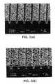
- FIGS. 3 ( a )-( d )are SEM photographs showing cross-sections of metallization layers plated exterior to respective semiconductor substrates wherein the metallization layers were deposited using incremental depositions at different current densities and thicknesses.
- FIG. 4is a SEM photograph showing a cross-section of a metallization layer plated exterior to a semiconductor substrate wherein the metallization layer was deposited using a pulse reverse waveform.
- FIG. 5is a SEM photograph showing a cross-section of a metallization layer plated exterior to a semiconductor substrate wherein the metallization layer was deposited using a two-step waveform comprised of an initial waveform having a low-current density followed by a further waveform having high-current density.
- FIG. 6is a SEM photograph showing a cross-section of a metallization layer plated exterior to a semiconductor substrate wherein the metallization layer was plated using the two-step waveform used to plate the metallization layer of FIG. 5, but wherein plating solution had a high copper concentration.
- FIGS. 7 and 8are SEM photographs showing cross-sections of metallization layers plated exterior to respective semiconductor substrates wherein the layers were deposited using a one-step waveform in a plating bath having organic additives.
- FIG. 9is a SEM photograph showing a cross-section of a metallization layer plated exterior to a semiconductor substrate wherein the metallization layer was plated using the one-step waveform used in the metallization process of FIGS. 7 and 8, but wherein the copper concentration of the plating solution has been reduced.
- FIGS. 10 ( a )- 10 ( c )are FIB photographs showing cross-sections of metallization layers plated exterior to respective semiconductor substrates wherein the metallization layers were plated using a plating bath having organic additives, and wherein the photographs illustrate the effect of seed layer quality on the plating process.
- the present inventioncan be understood with reference to the experiments disclosed herein. Although the experiments were performed in connection with the plating of a metal comprising copper, it will be recognized that the teachings disclosed herein are so applicable to the electroplating of other metals. All the experiments were performed on 200 mm wafers using a plating tool, such as a plating tool available from Semitool, Inc., of Kalispell, Mont. Three plating baths were examined. The first one, bath 1 (either 24 g/L or 36 g/L copper) had no organic additives. The bath 2 (Additive A) and the bath 2 (Additive B) contain organic additives from different vendors.
- FIG. 1presents a scanning electron microscope (“SEM”) cross-section obtained from bath 1 with 24 g/L copper. Voidfree fill was obtained for 0.5 ⁇ wide, 2:1 aspect ratio trench. The waveshape used was a forward pulse with 1 ms on and 1 ms off (WF 1 ). It was found that the waveshape was not significant for fill as long as the current density was low. As seen from FIG.
- an electroplating waveform having low current densityis used during the initial phases of the trench and/or via filling stage of the process. At some time subsequent to such initial filling, the electroplating waveform transitions to a higher current density waveform to complete the electroplating process and reduce the total time required for the process.
- the depositis smooth and very conformal. Compared to FIG. 2, where seam voids are observed, conformal plating is not sufficient to guarantee void-free fill because the top part of the trench is often pinched off first leaving voids inside.
- an initial low current density approachis necessary for gap fill if no-additive bath is used.
- initial low currentis helpful to improve the contact to the seed layer, particularly when the seed layer is very thin.
- the drawback of low currentis its long processing time.
- a plating recipe with multiple stepsis preferred in which a low current plating waveform is used to fill the small feature and, possibly, to enhance the seed layer, and then a high current plating waveform is used to finish the process and to provide smooth surface for one or more subsequent CMP processes.
- FIG. 5shows a cross-section obtained with a two-step waveform of 4 mA/cm 2 followed by 32 mA/cm 2 . An improvement in gap fill was observed. Using the same two-step waveform, an increase in the copper concentration (36 g/L) provided significant improvement of the fill process as illustrated in FIG. 6 .
- FIG. 7illustrates a metallization way are plated from such a bath using a 1-step waveform at 20 mA/cm 2 .
- FIG. 8is a cross-section obtained at 20 mA/cm 2 with 20 g/L copper in the solution. Although the surface of the deposit was smooth, similar to bath 3 , voids were observed in the trench at this copper concentration. As the copper concentration decreased from 20 to 10 g/L, void-free fill was obtained as in FIG. 9 .
- the better gap fill at lower copper concentration in the presence of organic additivesis different from that obtained for additive-free bath in which high copper provided better gap fill. This implies a different controlling mechanism for copper growth in the presence of additives. Similar to those obtained from additive-free bath, pulse reverse was found to produce voids and rough surface in this bath with additives.
- FIGS. 10 ( a )-( c )illustrates the effect of seed layer on the gap fill.
- the center voids(FIG. 10 a ) are formed when the top of the feature is pinched off before the filling is completed.
- the overhanging of the seed layer at the top of the featuredue to the line-of-sight deposition inherent in the PVD process, is often the main reason for the center voids and the insufficient suppressor of copper growth at the top of the trench during the plating is the other one.
- the formerneeds the optimization of the PVD process to deposit a conformal layer and may possibly require a combination of PVD process and other techniques such as CVD or electrochemical deposition for small features.
- the lattercalls for the optimization of the plating process by changing the bath composition and plating waveform.
- the bottom and sidewall voidsare mainly attributed to the insufficient coverage of the seed layer. Copper oxide is always formed on the seed layer prior to the plating when the wafer is exposed to air. This oxide is readily removed, and the underlying copper can be chemically etched when the wafer is in contact with the acidic plating solution. This may lead to the exposure of the barrier layer to the solution and result in the formation of bottom or sidewall voids. There are ways to eliminate these voids either by having a thick layer in the feature or using less aggressive plating solutions for the copper plating. By optimizing the seed layer, void-free gap fill was achieved as in FIG. 10 ( c ).
- An aspect of the present inventionprovides a method for depositing a metal into a micro-recessed structure on the surface of a microelectronic workpiece.
- the methodentails making contact between the surface of the microelectronic workpiece and the electroplating solution in an electroplating cell, the electroplating cell including a cathode formed by the surface of the microelectronic workpiece and an anode disposed in electrical contact with the electroplating solution.
- An initial film of the metalis deposited into the micro-recessed structure using a first current density for a first predetermined period of time. In one embodiment, the first current density is selected to enhance deposition of the metal at a bottom of the micro-recessed structure.
- the second current densityis selected to reduce the time required to substantially complete filling of the micro-recessed structure.
- the second current densityis substantially higher than the first current density used during initial deposition.
- the ratio of the first current density to the second current densityis about 1:8. In another embodiment, the ratio between the first current density and the second current density is about 1:10.
- the concentration of metal ions, such as copper, in the electroplating solutionis selected at a first concentration level for use in an electroplating bath including organic additives, or at a second higher concentration level for use in an electroplating bath that is substantially free of organic additives that are typically used, such as levelers or brighteners.
- the metal concentrationis suitably between 15 grams per liter and 36 grams per liter.
Landscapes
- Chemical & Material Sciences (AREA)
- Engineering & Computer Science (AREA)
- Metallurgy (AREA)
- Chemical Kinetics & Catalysis (AREA)
- Organic Chemistry (AREA)
- Materials Engineering (AREA)
- Electrochemistry (AREA)
- Microelectronics & Electronic Packaging (AREA)
- Condensed Matter Physics & Semiconductors (AREA)
- Power Engineering (AREA)
- General Physics & Mathematics (AREA)
- Computer Hardware Design (AREA)
- Physics & Mathematics (AREA)
- Manufacturing & Machinery (AREA)
- Electrodes Of Semiconductors (AREA)
- Internal Circuitry In Semiconductor Integrated Circuit Devices (AREA)
- Electroplating Methods And Accessories (AREA)
Abstract
Description
This application is a continuation of International PCT Application No. PCT/US99/23187, filed Oct. 5, 1999, which claims the benefit of U.S. Provisional Patent Application No. 60/103,061. filed Oct. 5, 1998, and is also a continuation-in-part of U.S. patent application Ser. No. 09/018,783, filed Feb. 4, 1998, the disclosures of which are hereby expressly incorporated by reference.
Not Applicable
An integrated circuit is an interconnected ensemble of devices formed within a semiconductor material and within a dielectric material that overlies a surface of the semiconductor material. Devices which may be formed within the semiconductor material include MOS transistors, bipolar transistors, diodes and diffused resistors. Devices which may be formed within the dielectric include thin-film resistors and capacitors. Typically, more than 100 integrated circuit die (IC chips) are constructed on a single 8 inch diameter silicon wafer. The devices utilized in each dice are interconnected by conductor paths formed within the dielectric. Typically, two or more levels of conductor paths, with successive levels separated by a dielectric layer, are employed as interconnections. In current practice, an aluminum alloy and silicon oxide are typically used for, respectively, the conductor and dielectric.
Delays in propagation of electrical signals between devices on a single dice limit the performance of integrated circuits. More particularly, these delays limit the speed at which an integrated circuit may process these electrical signals. Larger propagation delays reduce the speed at which the integrated circuit may process the electrical signals, while smaller propagation delays increase this speed. Accordingly, integrated circuit manufacturers seek ways in which to reduce the propagation delays.
For each interconnect path, signal propagation delay may be characterized by a time delay τ. See E. H. Stevens,Interconnect Technology, QMC, Inc., July 1993. An approximate expression for the time delay, τ, as it relates to the transmission of a signal between transistors on an integrated circuit is given by the equation:
In this equation, R and C are, respectively, an equivalent resistance and capacitance for the interconnect path, and ISATand VSATare, respectively, the saturation (maximum) current and the drain-to-source potential at the onset of current saturation for the transistor that applies a signal to the interconnect path. The path resistance is proportional to the resistivity, ρ, of the conductor material. The path capacitance is proportional to the relative dielectric permittivity, Ke, of the dielectric material. A small value of ρ requires that the interconnect line carry a current density sufficiently large to make the ratio VSAT//RISATsmall. It follows, therefore, that a low-ρ conductor which can carry a high current density and a low-Kedielectric should be utilized in the manufacture of high-performance integrated circuits.
To meet the foregoing criterion, copper interconnect lines within a low-Kedielectric will likely replace aluminum-alloy lines within a silicon oxide dielectric as the most preferred interconnect structure. See “Copper Goes Mainstream: Low-k to Follow”,Semiconductor international, November1997, pp. 67-70. Resistivities of copper films are in the range of 1.7 to 2.0 μΩcm. while resistivities of aluminum-alloy films are higher in the range of 3.0 to 3.5 μΩCm.
Despite the advantageous properties of copper, several problems must be addressed for copper interconnects to become viable in large-scale manufacturing processes.
Diffusion of copper is one such problem. Under the influence of an electric field, and at only moderately elevated temperatures, copper moves rapidly through silicon oxide. It is believed that copper also moves rapidly through low-Kedielectrics. Such copper diffusion causes failure of devices formed within the silicon.
Another problem is the propensity of copper to oxidize rapidly when immersed in aqueous solutions or when exposed to an oxygen-containing atmosphere. Oxidized surfaces of the copper are rendered non-conductive and thereby limit the current carrying capability of a given conductor path when compared to a similarly dimensioned non-oxidized copper path.
A still further problem with using copper in integrated circuits is that it is difficult to use copper in a multi-layer, integrated circuit structure with dielectric materials. Using traditional methods of copper deposition, copper adheres only weakly to dielectric materials.
Finally, because copper does not form volatile halide compounds, direct plasma etching of copper cannot be employed in fine-line patterning of copper. As such, copper is difficult to use in the increasingly small geometries required for advanced integrated circuit devices.
The semiconductor industry has addressed some of the foregoing problems and has adopted a generally standard interconnect architecture for copper interconnects. To this end, the industry has found that fine-line patterning of copper can be accomplished by etching trenches and vias in a dielectric, filling the trenches and vias with a deposition of copper, and removing copper from above the top surface of the dielectric by chemical-mechanical polishing (CMP). An interconnect architecture called dual damascene can be employed to implement such an architecture and thereby form copper lines within a dielectric. FIG. 1 illustrates the process steps generally required for implementing the dual damascene architecture.
Deposition of thin, uniform barrier and seed layers into high aspect ratio (depth/diameter) vias and high aspect ratio (depth/width) trenches is difficult. The upper portions of such trenches and vias tend to pinch-off before the respective trench and/or via is completely filled or layered with the desired material.
Electrodeposition of the copper metallization has been found to be the most efficient way to deposit copper into the trenches and vias. This method has been found to impart the best electromigration resistance performance to the resulting interconnect. However, this method of depositing the copper is not without problems of its own. For example, acid copper plating solutions for copper interconnect often contain organic additives to provide improved throwing power, enhanced leveling effect, and proper deposit characteristics. Since these additives play a significant role in copper plating, the concentrations of these additives in the plating bath need to be tightly controlled to ensure consistent trench fill and film properties. The present inventors have recognized that it would be desirable to use an additive-free plating solution to improve bath control, thereby eliminate the need to monitor the concentrations of the additives. Further, they have recognized that, even in the presence of such additives, certain plating parameters must be optimized.
The present inventors have found that application of metallization, particularly copper metallization, using low current density plating waveforms provides better trench and via filling results when compared to high current density plating waveforms. This is particularly true when additive-free plating solutions are used. However, such low current density plating waveforms are often quite slow in producing metal films of the requisite thickness. Accordingly, a low current density plating waveform is used during initial plating operations while a high current density plating waveform is used to decrease the fill time and, if desired, provide a different film morphology, some time after the initial plating operations are complete.
In accordance with one embodiment of the present invention, the waveshape and its frequency are used to influence the surface morphology of the copper metallization deposit Further, high metal concentrations in the additive-free plating solutions are used to provide more effective filling of the trench and via structures.
With respect to plating solutions that include additives, the present inventors have found that the plating process may be optimized by employing low metal concentration plating solutions. Such solutions produce higher quality filling of the trenches and vias when compared with copper metallization deposited using solutions having high metal concentrations.
Methods for depositing a metal into a micro-recessed structure in the surface of a microelectronic workpiece are disclosed. The methods are suitable for use in connection with additive free as well as additive containing electroplating solutions. In accordance with one embodiment, the method includes making contact between the surface of the microelectronic workpiece and an electroplating solution in an electroplating cell that includes a cathode formed by the surface of the microelectronic workpiece and an anode disposed in electrical contact with the electroplating solution. Next, an initial film of the metal is deposited into the micro-recessed structure using at least a first electroplating waveform having a first current density. The first current density of the first electroplating waveform is provide to enhance the deposition of the metal at a bottom of the micro-recessed structure. After the this initial plating, deposition of the metal is continued using at least a second electroplating waveform having a second current density. The second current density of the second electroplating waveform is provided to assist in reducing the time required to substantially complete filling of the micro-recessed structure.
FIG. 1 is a scanning electron microscope (“SEM”) photograph showing a cross-section of a metallization layer plated exterior to a semiconductor substrate wherein the metallization layer was deposited using a plating bath without organic additives and using a low-current plating waveform.
FIG. 2 is a SEM photograph showing a cross-section of a metallization layer plated exterior to a semiconductor substrate wherein the metallization layer was deposited using a plating bath without organic additives and using a high current density plating waveform.
FIGS.3(a)-(d) are SEM photographs showing cross-sections of metallization layers plated exterior to respective semiconductor substrates wherein the metallization layers were deposited using incremental depositions at different current densities and thicknesses.
FIG. 4 is a SEM photograph showing a cross-section of a metallization layer plated exterior to a semiconductor substrate wherein the metallization layer was deposited using a pulse reverse waveform.
FIG. 5 is a SEM photograph showing a cross-section of a metallization layer plated exterior to a semiconductor substrate wherein the metallization layer was deposited using a two-step waveform comprised of an initial waveform having a low-current density followed by a further waveform having high-current density.
FIG. 6 is a SEM photograph showing a cross-section of a metallization layer plated exterior to a semiconductor substrate wherein the metallization layer was plated using the two-step waveform used to plate the metallization layer of FIG. 5, but wherein plating solution had a high copper concentration.
FIGS. 7 and 8 are SEM photographs showing cross-sections of metallization layers plated exterior to respective semiconductor substrates wherein the layers were deposited using a one-step waveform in a plating bath having organic additives.
FIG. 9 is a SEM photograph showing a cross-section of a metallization layer plated exterior to a semiconductor substrate wherein the metallization layer was plated using the one-step waveform used in the metallization process of FIGS. 7 and 8, but wherein the copper concentration of the plating solution has been reduced.
FIGS.10(a)-10(c) are FIB photographs showing cross-sections of metallization layers plated exterior to respective semiconductor substrates wherein the metallization layers were plated using a plating bath having organic additives, and wherein the photographs illustrate the effect of seed layer quality on the plating process.
The present invention can be understood with reference to the experiments disclosed herein. Although the experiments were performed in connection with the plating of a metal comprising copper, it will be recognized that the teachings disclosed herein are so applicable to the electroplating of other metals. All the experiments were performed on 200 mm wafers using a plating tool, such as a plating tool available from Semitool, Inc., of Kalispell, Mont. Three plating baths were examined. The first one, bath1 (either 24 g/L or 36 g/L copper) had no organic additives. The bath2 (Additive A) and the bath2 (Additive B) contain organic additives from different vendors.
Good trench fill was obtained at low current density of 4 mA/cm2for copper concentrations from 15 to 36 g/L. It is believed that the high micro-throwing power at low current density due to low concentration polarization is responsible for such trench fill at high copper concentrations. FIG. 1 presents a scanning electron microscope (“SEM”) cross-section obtained frombath 1 with 24 g/L copper. Voidfree fill was obtained for 0.5 μ wide, 2:1 aspect ratio trench. The waveshape used was a forward pulse with 1 ms on and 1 ms off (WF1). It was found that the waveshape was not significant for fill as long as the current density was low. As seen from FIG. 1, rough surface or large grains were observed with 4 mA/cm2, implying that grain growth was the principal mechanism for the deposition as opposed to the formation of new nuclei. The copper deposit becomes smoother with high current density (40 mA/cm2) as shown in FIG.2. However, the fill at this higher current is not as good and seam voids were seen in the trench.
In view of the characteristics of the low current density and high current density waveforms, the present inventors have found that such waveforms can be combined during a single electroplating process whereby the advantages associated with each waveform are exploited to provide a submicron electroplating process that meets the process characteristics (void filling and time for filling) required to make it commercially viable. To this end, an electroplating waveform having low current density is used during the initial phases of the trench and/or via filling stage of the process. At some time subsequent to such initial filling, the electroplating waveform transitions to a higher current density waveform to complete the electroplating process and reduce the total time required for the process.
To understand how the copper was deposited inside trench and via features, incremental deposition at different current densities and thicknesses, represented as Ampere-minutes (A-min), was conducted. The results are compared in FIGS.3(a)-(d). At low current density, large grains were seen (FIGS.3(a) and (b)). As the thickness increased from 1.26 to 3.78 A-min, enhanced growth at the bottom of the trench is achieved, probably explaining why good fill was obtained in FIG. 1 at low current density. As such, the low-current density value should be chosen to provide enhanced growth of the copper metallization layer at the lower portions of the feature into which the copper metallization is deposited. At high current density (40 mA/cm2, FIGS.3(c) and (d)), the deposit is smooth and very conformal. Compared to FIG. 2, where seam voids are observed, conformal plating is not sufficient to guarantee void-free fill because the top part of the trench is often pinched off first leaving voids inside.
It is believed that the seam voids illustrated in these figures resulted from the overplating of copper deposit at the top of the feature due to its high current distribution. It is expected that the overplated copper will be preferentially removed if a reverse pulse is included in the waveshape. However, the addition of reverse pulses did not improve the trench fill as shown in FIG. 4 where seam voids were still observed even with a pulse reverse waveshape.
Therefore, an initial low current density approach is necessary for gap fill if no-additive bath is used. In addition to good trench fill, initial low current is helpful to improve the contact to the seed layer, particularly when the seed layer is very thin. However, the drawback of low current is its long processing time. To circumvent this, a plating recipe with multiple steps is preferred in which a low current plating waveform is used to fill the small feature and, possibly, to enhance the seed layer, and then a high current plating waveform is used to finish the process and to provide smooth surface for one or more subsequent CMP processes.
FIG. 5 shows a cross-section obtained with a two-step waveform of 4 mA/cm2followed by 32 mA/cm2. An improvement in gap fill was observed. Using the same two-step waveform, an increase in the copper concentration (36 g/L) provided significant improvement of the fill process as illustrated in FIG.6.
The effect of copper concentration on the gap fill for acidic baths with additives was examined using bath2 disclosed above. FIG. 7 illustrates a metallization way are plated from such a bath using a 1-step waveform at 20 mA/cm2. FIG. 8 is a cross-section obtained at 20 mA/cm2with 20 g/L copper in the solution. Although the surface of the deposit was smooth, similar to bath3, voids were observed in the trench at this copper concentration. As the copper concentration decreased from 20 to 10 g/L, void-free fill was obtained as in FIG.9. The better gap fill at lower copper concentration in the presence of organic additives is different from that obtained for additive-free bath in which high copper provided better gap fill. This implies a different controlling mechanism for copper growth in the presence of additives. Similar to those obtained from additive-free bath, pulse reverse was found to produce voids and rough surface in this bath with additives.
FIGS.10(a)-(c) illustrates the effect of seed layer on the gap fill. The center voids (FIG. 10a) are formed when the top of the feature is pinched off before the filling is completed. The overhanging of the seed layer at the top of the feature, due to the line-of-sight deposition inherent in the PVD process, is often the main reason for the center voids and the insufficient suppressor of copper growth at the top of the trench during the plating is the other one. The former needs the optimization of the PVD process to deposit a conformal layer and may possibly require a combination of PVD process and other techniques such as CVD or electrochemical deposition for small features. The latter calls for the optimization of the plating process by changing the bath composition and plating waveform.
The bottom and sidewall voids (FIG.10(b)) are mainly attributed to the insufficient coverage of the seed layer. Copper oxide is always formed on the seed layer prior to the plating when the wafer is exposed to air. This oxide is readily removed, and the underlying copper can be chemically etched when the wafer is in contact with the acidic plating solution. This may lead to the exposure of the barrier layer to the solution and result in the formation of bottom or sidewall voids. There are ways to eliminate these voids either by having a thick layer in the feature or using less aggressive plating solutions for the copper plating. By optimizing the seed layer, void-free gap fill was achieved as in FIG.10(c).
An aspect of the present invention provides a method for depositing a metal into a micro-recessed structure on the surface of a microelectronic workpiece. The method entails making contact between the surface of the microelectronic workpiece and the electroplating solution in an electroplating cell, the electroplating cell including a cathode formed by the surface of the microelectronic workpiece and an anode disposed in electrical contact with the electroplating solution. An initial film of the metal is deposited into the micro-recessed structure using a first current density for a first predetermined period of time. In one embodiment, the first current density is selected to enhance deposition of the metal at a bottom of the micro-recessed structure. After the initial deposition, deposition of the metal is continued for a second period of time using a second current density. In one aspect of the invention, the second current density is selected to reduce the time required to substantially complete filling of the micro-recessed structure. In another aspect of the invention, the second current density is substantially higher than the first current density used during initial deposition. In one embodiment of the invention, the ratio of the first current density to the second current density is about 1:8. In another embodiment, the ratio between the first current density and the second current density is about 1:10.
In a still further aspect of the present invention, the concentration of metal ions, such as copper, in the electroplating solution is selected at a first concentration level for use in an electroplating bath including organic additives, or at a second higher concentration level for use in an electroplating bath that is substantially free of organic additives that are typically used, such as levelers or brighteners. In the instance of the substantially additive free bath, the metal concentration is suitably between 15 grams per liter and 36 grams per liter.
Claims (22)
1. A method for depositing a metal into a micro-recessed structure in the surface of a microelectronic workpiece, the method comprising:
making contact between the surface of the microelectronic workpiece and an electroplating solution in an electroplating cell, the electroplating cell including a cathode formed by the surface of the microelectronic workpiece and an anode disposed in electrical contact with the electroplating solution;
depositing an initial film of the metal into the micro-recessed structure using a first current density for a first predetermined period of time, the first current density assisting to enhance deposition of the metal at a bottom of the micro-recessed structure;
continuing deposition of the metal beginning at least some time after the first predetermined period of time using a second current density, the second current density assisting to reduce the time required to substantially complete filling of the micro-recessed structure, the second current density being greater than the first current density.
2. A method as claimed inclaim 1 wherein the electroplating solution is substantially free of organic additives and has a first predetermined concentration of the metal that is to be electroplated that is higher than a second predetermined concentration suitable for use in a plating bath including organic additives.
3. A method as claimed inclaim 1 wherein the metal that is to be plated comprises copper.
4. A method as claimed inclaim 1 wherein the ratio between the first current density and the second current density is about 1:10.
5. A method as claimed inclaim 1 wherein the ratio between the first current density and the second current density is about 1:8.
6. A method for depositing a metal into a micro-recessed structure in the surface of a microelectronic workpiece, the method comprising:
making contact between the surface of the microelectronic workpiece and an electroplating solution in an electroplating cell, the electroplating cell including a cathode formed by the surface of the microelectronic workpiece and an anode disposed in electrical contact with the electroplating solution;
depositing an initial film of the metal into the micro-recessed structure using a first current density for a first predetermined period of time to enhance growth of the metal at the bottom of the micro-recessed structure;
at least substantially completing the fill of the micro-recessed structure using a second current density for a second predetermined period of time, the second current density being substantially higher than the first current density.
7. A method as claimed inclaim 6 wherein the electroplating solution is free of organic additives and has a first predetermined concentration of metal ions that are to be deposited in the micro-recessed structure that is higher than a second predetermined concentration of metal ions that would be used for deposition in the presence of organic additives.
8. A method as claimed inclaim 7 wherein the first predetermined period of time is on the order of 30 seconds.
9. A method as claimed inclaim 6 wherein the metal that is to be plated comprises copper.
10. A method as claimed inclaim 7 wherein the electroplating solution comprises a concentration of the metal that is between about 15 g/L and 36 g/L.
11. A method as claimed inclaim 9 wherein the electroplating solution comprises a concentration of copper that is between about 15 g/L and 36 g/L.
12. A method as claimed inclaim 6 wherein the ratio between the first current density and the second current density is about 1:10.
13. A method as claimed inclaim 6 wherein the ratio between the first current density and the second current density is about 1:8.
14. A method as claimed inclaim 6 wherein the first electroplating waveform is a pulsed waveform.
15. A method ofclaim 1 , wherein the micro-recessed structure has a sub-micron width.
16. The process ofclaim 15 , wherein the micro-recessed structure has a width of approximately 0.5 microns.
17. The process ofclaim 15 , wherein the micro-recessed structure has an aspect ratio of 2:1.
18. The process ofclaim 6 , wherein the initial film of metal deposited using the first current density has a first morphology, and the second metal deposited using the second current density has a second morphology that is different than the first morphology.
19. The process ofclaim 6 , further comprising depositing a thin seed layer on the microelectronic workpiece prior to deposition of the initial film deposition of the initial film enhancing the thin seed layer.
20. The method ofclaim 6 , further comprising, after processing the micro-recessed structure with the second electroplating waveform, processing the micro-recessed structure using a third electroplating waveform including a reverse current pulse to remove overfill.
21. A method for depositing a metal onto the surface of a microelectronic workpiece, the method comprising:
placing the surface of the microelectronic workpiece in contact with an electroplating solution including a metal ion to be deposited and that is substantially free of organic additives;
supplying plating power between the surface of the microelectronic workpiece and an anode disposed in contact with the electroplating solution to deposit metal onto the surface of the microelectronic workpiece, wherein metal is first deposited in an initial amount using a first current density for a first predetermined period of time to enhance growth of the metal at the bottom of the micro-recessed structure, and then additional metal is deposited onto the initial amount of metal using a second current density for a second predetermined period of time, the second current density being substantially higher than the first current density, wherein the concentration of the metal ion in the electroplating solution is provided at a first predetermined concentration level that is higher than a second predetermined concentration level that would be utilized for metal deposition in the presence of organic additives.
22. A method of depositing a metal layer on a semiconductor wafer comprising:
depositing a seed layer on a surface of the water;
immersing the water in an electrolytic solution containing metal ions;
biasing the wafer negatively with respect to the electrolytic solution so as to create a current flow at a first nominal current density between an anode and the wafer to thereby deposit a plated layer electrolytically on the seed layer of the wafer for enhancing growth of the metal at the bottom of the micro-recessed structure; and
increasing the current flow to a second nominal current density greater than the first nominal current density after a predetermined time period has elapsed.
Priority Applications (3)
| Application Number | Priority Date | Filing Date | Title |
|---|---|---|---|
| US09/815,931US6806186B2 (en) | 1998-02-04 | 2001-03-23 | Submicron metallization using electrochemical deposition |
| US10/882,664US7144805B2 (en) | 1998-02-04 | 2004-07-01 | Method of submicron metallization using electrochemical deposition of recesses including a first deposition at a first current density and a second deposition at an increased current density |
| US11/439,720US20060208272A1 (en) | 1998-02-04 | 2006-05-23 | Method for filling recessed micro-structures with metallization in the production of a microelectronic device |
Applications Claiming Priority (4)
| Application Number | Priority Date | Filing Date | Title |
|---|---|---|---|
| US09/018,783US7244677B2 (en) | 1998-02-04 | 1998-02-04 | Method for filling recessed micro-structures with metallization in the production of a microelectronic device |
| US10306198P | 1998-10-05 | 1998-10-05 | |
| PCT/US1999/023187WO2000020662A1 (en) | 1998-10-05 | 1999-10-05 | Submicron metallization using electrochemical deposition |
| US09/815,931US6806186B2 (en) | 1998-02-04 | 2001-03-23 | Submicron metallization using electrochemical deposition |
Related Parent Applications (4)
| Application Number | Title | Priority Date | Filing Date |
|---|---|---|---|
| US09/018,783ContinuationUS7244677B2 (en) | 1998-02-04 | 1998-02-04 | Method for filling recessed micro-structures with metallization in the production of a microelectronic device |
| US09/018,783Continuation-In-PartUS7244677B2 (en) | 1998-02-04 | 1998-02-04 | Method for filling recessed micro-structures with metallization in the production of a microelectronic device |
| PCT/US1999/023187ContinuationWO2000020662A1 (en) | 1998-02-04 | 1999-10-05 | Submicron metallization using electrochemical deposition |
| PCT/US1999/023189ContinuationWO2000020946A2 (en) | 1998-02-04 | 1999-10-05 | Inflatable and collapsible screen |
Related Child Applications (1)
| Application Number | Title | Priority Date | Filing Date |
|---|---|---|---|
| US10/882,664ContinuationUS7144805B2 (en) | 1998-02-04 | 2004-07-01 | Method of submicron metallization using electrochemical deposition of recesses including a first deposition at a first current density and a second deposition at an increased current density |
Publications (2)
| Publication Number | Publication Date |
|---|---|
| US20020004301A1 US20020004301A1 (en) | 2002-01-10 |
| US6806186B2true US6806186B2 (en) | 2004-10-19 |
Family
ID=21789765
Family Applications (7)
| Application Number | Title | Priority Date | Filing Date |
|---|---|---|---|
| US09/018,783Expired - Fee RelatedUS7244677B2 (en) | 1998-02-04 | 1998-02-04 | Method for filling recessed micro-structures with metallization in the production of a microelectronic device |
| US09/815,931Expired - Fee RelatedUS6806186B2 (en) | 1998-02-04 | 2001-03-23 | Submicron metallization using electrochemical deposition |
| US09/880,715AbandonedUS20030045095A1 (en) | 1998-02-04 | 2001-06-12 | Method for filling recessed micro-structures with metallization in the production of a microelectronic device |
| US10/112,166Expired - LifetimeUS6753251B2 (en) | 1998-02-04 | 2002-03-28 | Method for filling recessed micro-structures with metallization in the production of a microelectronic device |
| US10/882,664Expired - Fee RelatedUS7144805B2 (en) | 1998-02-04 | 2004-07-01 | Method of submicron metallization using electrochemical deposition of recesses including a first deposition at a first current density and a second deposition at an increased current density |
| US11/439,720AbandonedUS20060208272A1 (en) | 1998-02-04 | 2006-05-23 | Method for filling recessed micro-structures with metallization in the production of a microelectronic device |
| US11/593,362AbandonedUS20070114133A1 (en) | 1998-02-04 | 2006-11-06 | Method for filling recessed micro-structures with metallization in the production of a microelectronic device |
Family Applications Before (1)
| Application Number | Title | Priority Date | Filing Date |
|---|---|---|---|
| US09/018,783Expired - Fee RelatedUS7244677B2 (en) | 1998-02-04 | 1998-02-04 | Method for filling recessed micro-structures with metallization in the production of a microelectronic device |
Family Applications After (5)
| Application Number | Title | Priority Date | Filing Date |
|---|---|---|---|
| US09/880,715AbandonedUS20030045095A1 (en) | 1998-02-04 | 2001-06-12 | Method for filling recessed micro-structures with metallization in the production of a microelectronic device |
| US10/112,166Expired - LifetimeUS6753251B2 (en) | 1998-02-04 | 2002-03-28 | Method for filling recessed micro-structures with metallization in the production of a microelectronic device |
| US10/882,664Expired - Fee RelatedUS7144805B2 (en) | 1998-02-04 | 2004-07-01 | Method of submicron metallization using electrochemical deposition of recesses including a first deposition at a first current density and a second deposition at an increased current density |
| US11/439,720AbandonedUS20060208272A1 (en) | 1998-02-04 | 2006-05-23 | Method for filling recessed micro-structures with metallization in the production of a microelectronic device |
| US11/593,362AbandonedUS20070114133A1 (en) | 1998-02-04 | 2006-11-06 | Method for filling recessed micro-structures with metallization in the production of a microelectronic device |
Country Status (1)
| Country | Link |
|---|---|
| US (7) | US7244677B2 (en) |
Cited By (13)
| Publication number | Priority date | Publication date | Assignee | Title |
|---|---|---|---|---|
| US20040000488A1 (en)* | 2002-06-28 | 2004-01-01 | Applied Materials, Inc. | CU ECP planarization by insertion of polymer treatment step between gap fill and bulk fill steps |
| US20040149584A1 (en)* | 2002-12-27 | 2004-08-05 | Mizuki Nagai | Plating method |
| US20040262165A1 (en)* | 2003-04-16 | 2004-12-30 | Hiroyuki Kanda | Plating method |
| US20060283716A1 (en)* | 2003-07-08 | 2006-12-21 | Hooman Hafezi | Method of direct plating of copper on a ruthenium alloy |
| US20070062818A1 (en)* | 2005-09-20 | 2007-03-22 | Alchimer | Electroplating composition intended for coating a surface of a substrate with a metal |
| US20070062817A1 (en)* | 2005-09-20 | 2007-03-22 | Alchimer | Method of coating a surface of a substrate with a metal by electroplating |
| US20070125657A1 (en)* | 2003-07-08 | 2007-06-07 | Zhi-Wen Sun | Method of direct plating of copper on a substrate structure |
| US20090139870A1 (en)* | 2007-12-04 | 2009-06-04 | Mizuki Nagai | Plating apparatus and plating method |
| US20090148677A1 (en)* | 2007-12-10 | 2009-06-11 | International Business Machines Corporation | High aspect ratio electroplated metal feature and method |
| US7654221B2 (en) | 2003-10-06 | 2010-02-02 | Applied Materials, Inc. | Apparatus for electroless deposition of metals onto semiconductor substrates |
| US7670465B2 (en) | 2002-07-24 | 2010-03-02 | Applied Materials, Inc. | Anolyte for copper plating |
| US7827930B2 (en) | 2004-01-26 | 2010-11-09 | Applied Materials, Inc. | Apparatus for electroless deposition of metals onto semiconductor substrates |
| US9376758B2 (en) | 2010-12-21 | 2016-06-28 | Ebara Corporation | Electroplating method |
Families Citing this family (60)
| Publication number | Priority date | Publication date | Assignee | Title |
|---|---|---|---|---|
| US6276072B1 (en) | 1997-07-10 | 2001-08-21 | Applied Materials, Inc. | Method and apparatus for heating and cooling substrates |
| US7244677B2 (en) | 1998-02-04 | 2007-07-17 | Semitool. Inc. | Method for filling recessed micro-structures with metallization in the production of a microelectronic device |
| US6261433B1 (en)* | 1998-04-21 | 2001-07-17 | Applied Materials, Inc. | Electro-chemical deposition system and method of electroplating on substrates |
| EP1091024A4 (en)* | 1998-04-30 | 2006-03-22 | Ebara Corp | Method and device for plating substrate |
| US6497801B1 (en)* | 1998-07-10 | 2002-12-24 | Semitool Inc | Electroplating apparatus with segmented anode array |
| US7192494B2 (en)* | 1999-03-05 | 2007-03-20 | Applied Materials, Inc. | Method and apparatus for annealing copper films |
| US7189318B2 (en)* | 1999-04-13 | 2007-03-13 | Semitool, Inc. | Tuning electrodes used in a reactor for electrochemically processing a microelectronic workpiece |
| US20030038035A1 (en)* | 2001-05-30 | 2003-02-27 | Wilson Gregory J. | Methods and systems for controlling current in electrochemical processing of microelectronic workpieces |
| TWI226387B (en)* | 1999-04-13 | 2005-01-11 | Semitool Inc | Workpiece processor having processing chamber with improved processing fluid flow |
| US7020537B2 (en)* | 1999-04-13 | 2006-03-28 | Semitool, Inc. | Tuning electrodes used in a reactor for electrochemically processing a microelectronic workpiece |
| US7438788B2 (en)* | 1999-04-13 | 2008-10-21 | Semitool, Inc. | Apparatus and methods for electrochemical processing of microelectronic workpieces |
| US6916412B2 (en)* | 1999-04-13 | 2005-07-12 | Semitool, Inc. | Adaptable electrochemical processing chamber |
| US7264698B2 (en)* | 1999-04-13 | 2007-09-04 | Semitool, Inc. | Apparatus and methods for electrochemical processing of microelectronic workpieces |
| US7388289B1 (en)* | 1999-09-02 | 2008-06-17 | Micron Technology, Inc. | Local multilayered metallization |
| US6660139B1 (en)* | 1999-11-08 | 2003-12-09 | Ebara Corporation | Plating apparatus and method |
| US20050183959A1 (en)* | 2000-04-13 | 2005-08-25 | Wilson Gregory J. | Tuning electrodes used in a reactor for electrochemically processing a microelectric workpiece |
| WO2001084621A1 (en)* | 2000-04-27 | 2001-11-08 | Ebara Corporation | Rotation holding device and semiconductor substrate processing device |
| KR100800531B1 (en) | 2000-06-30 | 2008-02-04 | 가부시키가이샤 에바라 세이사꾸쇼 | Copper Plating Solution, Plating Method and Plating Equipment |
| WO2002004887A1 (en) | 2000-07-08 | 2002-01-17 | Semitool, Inc. | Methods and apparatus for processing microelectronic workpieces using metrology |
| US6436267B1 (en)* | 2000-08-29 | 2002-08-20 | Applied Materials, Inc. | Method for achieving copper fill of high aspect ratio interconnect features |
| US6432821B1 (en)* | 2000-12-18 | 2002-08-13 | Intel Corporation | Method of copper electroplating |
| US20050061676A1 (en)* | 2001-03-12 | 2005-03-24 | Wilson Gregory J. | System for electrochemically processing a workpiece |
| US7090751B2 (en)* | 2001-08-31 | 2006-08-15 | Semitool, Inc. | Apparatus and methods for electrochemical processing of microelectronic workpieces |
| US20030146102A1 (en)* | 2002-02-05 | 2003-08-07 | Applied Materials, Inc. | Method for forming copper interconnects |
| CA2479873A1 (en)* | 2002-04-12 | 2003-10-23 | Acm Research, Inc. | Electropolishing and electroplating methods |
| US20040108212A1 (en)* | 2002-12-06 | 2004-06-10 | Lyndon Graham | Apparatus and methods for transferring heat during chemical processing of microelectronic workpieces |
| US20040154926A1 (en)* | 2002-12-24 | 2004-08-12 | Zhi-Wen Sun | Multiple chemistry electrochemical plating method |
| JP4066820B2 (en)* | 2003-01-17 | 2008-03-26 | 豊田合成株式会社 | Manufacturing method for forming wiring layer mainly composed of copper (Cu) on semiconductor |
| US7001840B1 (en)* | 2003-02-10 | 2006-02-21 | Advanced Micro Devices, Inc. | Interconnect with multiple layers of conductive material with grain boundary between the layers |
| US7311810B2 (en)* | 2003-04-18 | 2007-12-25 | Applied Materials, Inc. | Two position anneal chamber |
| US7473339B2 (en)* | 2003-04-18 | 2009-01-06 | Applied Materials, Inc. | Slim cell platform plumbing |
| US7465661B2 (en)* | 2003-05-28 | 2008-12-16 | The United States Of America As Represented By The Secretary Of The Navy | High aspect ratio microelectrode arrays |
| US7122466B2 (en)* | 2003-07-28 | 2006-10-17 | Texas Instruments Incorporated | Two step semiconductor manufacturing process for copper interconnects |
| CN100512603C (en)* | 2003-09-09 | 2009-07-08 | Hoya株式会社 | Method for manufacturing double-sided printed glass board |
| US20050092611A1 (en)* | 2003-11-03 | 2005-05-05 | Semitool, Inc. | Bath and method for high rate copper deposition |
| US20060009047A1 (en)* | 2004-07-09 | 2006-01-12 | Wirth Paul Z | Modular tool unit for processing microelectronic workpieces |
| KR100640955B1 (en)* | 2004-12-29 | 2006-11-02 | 동부일렉트로닉스 주식회사 | Metal Wiring of Semiconductor Devices and Formation Method |
| KR100639073B1 (en)* | 2005-05-10 | 2006-10-30 | 한국과학기술원 | Method of forming semiconductor metal wiring using selective damascene |
| KR100617070B1 (en)* | 2005-09-13 | 2006-08-30 | 동부일렉트로닉스 주식회사 | Method for Cleaning Electrochemical Plating Cells |
| JP4764718B2 (en)* | 2005-12-28 | 2011-09-07 | 新光電気工業株式会社 | Through-hole filling method |
| US7666787B2 (en)* | 2006-02-21 | 2010-02-23 | International Business Machines Corporation | Grain growth promotion layer for semiconductor interconnect structures |
| KR100854910B1 (en)* | 2006-12-28 | 2008-08-28 | 주식회사 하이닉스반도체 | Metal wiring formation method of semiconductor device |
| US7656493B2 (en)* | 2007-07-31 | 2010-02-02 | Arthur Alan R | Pixel well electrodes |
| US7956463B2 (en)* | 2009-09-16 | 2011-06-07 | International Business Machines Corporation | Large grain size conductive structure for narrow interconnect openings |
| US9714474B2 (en)* | 2010-04-06 | 2017-07-25 | Tel Nexx, Inc. | Seed layer deposition in microscale features |
| US8661664B2 (en) | 2010-07-19 | 2014-03-04 | International Business Machines Corporation | Techniques for forming narrow copper filled vias having improved conductivity |
| US8617982B2 (en)* | 2010-10-05 | 2013-12-31 | Novellus Systems, Inc. | Subtractive patterning to define circuit components |
| US8525339B2 (en) | 2011-07-27 | 2013-09-03 | International Business Machines Corporation | Hybrid copper interconnect structure and method of fabricating same |
| US9418937B2 (en) | 2011-12-09 | 2016-08-16 | Infineon Technologies Ag | Integrated circuit and method of forming an integrated circuit |
| US8796853B2 (en) | 2012-02-24 | 2014-08-05 | International Business Machines Corporation | Metallic capped interconnect structure with high electromigration resistance and low resistivity |
| US9312203B2 (en) | 2013-01-02 | 2016-04-12 | Globalfoundries Inc. | Dual damascene structure with liner |
| KR102049569B1 (en) | 2013-08-01 | 2019-11-28 | 삼성디스플레이 주식회사 | Method for constituting structure including micro pattern, method for constituting nano pattern, and method for manufacturing display panel for liquid crystal display |
| JP6350064B2 (en)* | 2013-10-09 | 2018-07-04 | 日立化成株式会社 | Manufacturing method of multilayer wiring board |
| US9899234B2 (en) | 2014-06-30 | 2018-02-20 | Lam Research Corporation | Liner and barrier applications for subtractive metal integration |
| US10154598B2 (en) | 2014-10-13 | 2018-12-11 | Rohm And Haas Electronic Materials Llc | Filling through-holes |
| US9735051B2 (en) | 2015-12-14 | 2017-08-15 | International Business Machines Corporation | Semiconductor device interconnect structures formed by metal reflow process |
| US10329683B2 (en) | 2016-11-03 | 2019-06-25 | Lam Research Corporation | Process for optimizing cobalt electrofill using sacrificial oxidants |
| US11152294B2 (en) | 2018-04-09 | 2021-10-19 | Corning Incorporated | Hermetic metallized via with improved reliability |
| WO2020061437A1 (en)* | 2018-09-20 | 2020-03-26 | Industrial Technology Research Institute | Copper metallization for through-glass vias on thin glass |
| CN113474311B (en) | 2019-02-21 | 2023-12-29 | 康宁股份有限公司 | Glass or glass ceramic article with copper-metallized through-holes and process for making same |
Citations (204)
| Publication number | Priority date | Publication date | Assignee | Title |
|---|---|---|---|---|
| US2443599A (en) | 1942-05-04 | 1948-06-22 | Poor & Co | Electroplating method employing pulsating current of adjustable wave form |
| US3267010A (en) | 1962-04-16 | 1966-08-16 | Udylite Corp | Electrodeposition of copper from acidic baths |
| US3328273A (en) | 1966-08-15 | 1967-06-27 | Udylite Corp | Electro-deposition of copper from acidic baths |
| US3658663A (en) | 1970-03-03 | 1972-04-25 | Japan Electro Plating Co | Method for effecting partial metal plating |
| US3664933A (en) | 1969-06-19 | 1972-05-23 | Udylite Corp | Process for acid copper plating of zinc |
| US3706635A (en) | 1971-11-15 | 1972-12-19 | Monsanto Co | Electrochemical compositions and processes |
| US3715289A (en) | 1971-02-08 | 1973-02-06 | Stauffer Chemical Co | Brightener composition for acid copper electroplating baths |
| US3716462A (en) | 1970-10-05 | 1973-02-13 | D Jensen | Copper plating on zinc and its alloys |
| US3727620A (en) | 1970-03-18 | 1973-04-17 | Fluoroware Of California Inc | Rinsing and drying device |
| US3770598A (en) | 1972-01-21 | 1973-11-06 | Oxy Metal Finishing Corp | Electrodeposition of copper from acid baths |
| US3862891A (en) | 1973-09-24 | 1975-01-28 | Gte Automatic Electric Lab Inc | Uniform plating current apparatus and method |
| US3878066A (en) | 1972-09-06 | 1975-04-15 | Manfred Dettke | Bath for galvanic deposition of gold and gold alloys |
| US3894918A (en) | 1973-12-20 | 1975-07-15 | Western Electric Co | Methods of treating portions of articles |
| US3930963A (en) | 1971-07-29 | 1976-01-06 | Photocircuits Division Of Kollmorgen Corporation | Method for the production of radiant energy imaged printed circuit boards |
| US3990926A (en) | 1971-08-30 | 1976-11-09 | Perstorp Ab | Method for the production of material for printed circuits |
| US4000046A (en) | 1974-12-23 | 1976-12-28 | P. R. Mallory & Co., Inc. | Method of electroplating a conductive layer over an electrolytic capacitor |
| US4027686A (en) | 1973-01-02 | 1977-06-07 | Texas Instruments Incorporated | Method and apparatus for cleaning the surface of a semiconductor slice with a liquid spray of de-ionized water |
| US4030015A (en) | 1975-10-20 | 1977-06-14 | International Business Machines Corporation | Pulse width modulated voltage regulator-converter/power converter having push-push regulator-converter means |
| US4043877A (en) | 1975-03-19 | 1977-08-23 | Siemens Aktiengesellschaft | Method for the manufacture of microscopically small metal or metal-alloy structures |
| US4065374A (en) | 1976-08-10 | 1977-12-27 | New Nippon Electric Co., Ltd. | Method and apparatus for plating under constant current density |
| US4092176A (en) | 1975-12-11 | 1978-05-30 | Nippon Electric Co., Ltd. | Apparatus for washing semiconductor wafers |
| US4100054A (en) | 1977-03-11 | 1978-07-11 | Essex Group, Inc. | Combination insulating sleeve and electrical contact member for electro-plating rack |
| US4110176A (en) | 1975-03-11 | 1978-08-29 | Oxy Metal Industries Corporation | Electrodeposition of copper |
| US4113492A (en) | 1976-04-08 | 1978-09-12 | Fuji Photo Film Co., Ltd. | Spin coating process |
| US4134802A (en) | 1977-10-03 | 1979-01-16 | Oxy Metal Industries Corporation | Electrolyte and method for electrodepositing bright metal deposits |
| US4250004A (en) | 1980-02-25 | 1981-02-10 | Olin Corporation | Process for the preparation of low overvoltage electrodes |
| US4272335A (en) | 1980-02-19 | 1981-06-09 | Oxy Metal Industries Corporation | Composition and method for electrodeposition of copper |
| US4279948A (en) | 1978-05-25 | 1981-07-21 | Macdermid Incorporated | Electroless copper deposition solution using a hypophosphite reducing agent |
| US4315059A (en) | 1980-07-18 | 1982-02-09 | The United States Of America As Represented By The United States Department Of Energy | Molten salt lithium cells |
| US4336114A (en) | 1981-03-26 | 1982-06-22 | Hooker Chemicals & Plastics Corp. | Electrodeposition of bright copper |
| US4376685A (en) | 1981-06-24 | 1983-03-15 | M&T Chemicals Inc. | Acid copper electroplating baths containing brightening and leveling additives |
| US4384930A (en) | 1981-08-21 | 1983-05-24 | Mcgean-Rohco, Inc. | Electroplating baths, additives therefor and methods for the electrodeposition of metals |
| US4385978A (en) | 1981-09-14 | 1983-05-31 | Rca Corporation | Cathode head |
| US4401521A (en) | 1980-11-28 | 1983-08-30 | Asahi Kasei Kogyo Kabushiki Kaisha | Method for manufacturing a fine-patterned thick film conductor structure |
| US4405416A (en) | 1980-07-18 | 1983-09-20 | Raistrick Ian D | Molten salt lithium cells |
| US4428815A (en) | 1983-04-28 | 1984-01-31 | Western Electric Co., Inc. | Vacuum-type article holder and methods of supportively retaining articles |
| US4435266A (en) | 1981-10-01 | 1984-03-06 | Emi Limited | Electroplating arrangements |
| US4443117A (en) | 1980-09-26 | 1984-04-17 | Terumo Corporation | Measuring apparatus, method of manufacture thereof, and method of writing data into same |
| US4475823A (en) | 1982-04-09 | 1984-10-09 | Piezo Electric Products, Inc. | Self-calibrating thermometer |
| US4489740A (en) | 1982-12-27 | 1984-12-25 | General Signal Corporation | Disc cleaning machine |
| US4510176A (en) | 1983-09-26 | 1985-04-09 | At&T Bell Laboratories | Removal of coating from periphery of a semiconductor wafer |
| US4514265A (en) | 1984-07-05 | 1985-04-30 | Rca Corporation | Bonding pads for semiconductor devices |
| US4518678A (en) | 1983-12-16 | 1985-05-21 | Advanced Micro Devices, Inc. | Selective removal of coating material on a coated substrate |
| US4519846A (en) | 1984-03-08 | 1985-05-28 | Seiichiro Aigo | Process for washing and drying a semiconductor element |
| US4539222A (en) | 1983-11-30 | 1985-09-03 | International Business Machines Corporation | Process for forming metal patterns wherein metal is deposited on a thermally depolymerizable polymer and selectively removed |
| US4576689A (en) | 1979-06-19 | 1986-03-18 | Makkaev Almaxud M | Process for electrochemical metallization of dielectrics |
| US4624749A (en) | 1985-09-03 | 1986-11-25 | Harris Corporation | Electrodeposition of submicrometer metallic interconnect for integrated circuits |
| US4687552A (en) | 1985-12-02 | 1987-08-18 | Tektronix, Inc. | Rhodium capped gold IC metallization |
| US4693805A (en) | 1986-02-14 | 1987-09-15 | Boe Limited | Method and apparatus for sputtering a dielectric target or for reactive sputtering |
| US4732785A (en) | 1986-09-26 | 1988-03-22 | Motorola, Inc. | Edge bead removal process for spin on films |
| US4781801A (en) | 1987-02-03 | 1988-11-01 | Mcgean-Rohco, Inc. | Method of copper plating gravure rolls |
| US4810333A (en) | 1987-12-14 | 1989-03-07 | Shipley Company Inc. | Electroplating process |
| US4869971A (en) | 1986-05-22 | 1989-09-26 | Nee Chin Cheng | Multilayer pulsed-current electrodeposition process |
| US4879007A (en) | 1988-12-12 | 1989-11-07 | Process Automation Int'l Ltd. | Shield for plating bath |
| US4891069A (en) | 1986-06-06 | 1990-01-02 | Techno Instruments Investments 1983 Ltd. | Composition for the electrolytic coating of circuit boards without an electroless metal coating |
| US4898647A (en) | 1985-12-24 | 1990-02-06 | Gould, Inc. | Process and apparatus for electroplating copper foil |
| US4951601A (en) | 1986-12-19 | 1990-08-28 | Applied Materials, Inc. | Multi-chamber integrated process system |
| US4959278A (en) | 1988-06-16 | 1990-09-25 | Nippon Mining Co., Ltd. | Tin whisker-free tin or tin alloy plated article and coating technique thereof |
| US4979464A (en) | 1987-06-15 | 1990-12-25 | Convac Gmbh | Apparatus for treating wafers in the manufacture of semiconductor elements |
| US4990224A (en) | 1988-12-21 | 1991-02-05 | International Business Machines Corporation | Copper plating bath and process for difficult to plate metals |
| US5000827A (en) | 1990-01-02 | 1991-03-19 | Motorola, Inc. | Method and apparatus for adjusting plating solution flow characteristics at substrate cathode periphery to minimize edge effect |
| US5021129A (en) | 1989-09-25 | 1991-06-04 | International Business Machines Corporation | Multilayer structures of different electroactive materials and methods of fabrication thereof |
| US5039381A (en) | 1989-05-25 | 1991-08-13 | Mullarkey Edward J | Method of electroplating a precious metal on a semiconductor device, integrated circuit or the like |
| US5055425A (en) | 1989-06-01 | 1991-10-08 | Hewlett-Packard Company | Stacked solid via formation in integrated circuit systems |
| US5084412A (en) | 1989-10-02 | 1992-01-28 | Kabushiki Kaisha Toshiba | Method of manufacturing a semiconductor device with a copper wiring layer |
| US5091339A (en) | 1990-07-23 | 1992-02-25 | Microelectronics And Computer Technology Corporation | Trenching techniques for forming vias and channels in multilayer electrical interconnects |
| US5115430A (en) | 1990-09-24 | 1992-05-19 | At&T Bell Laboratories | Fair access of multi-priority traffic to distributed-queue dual-bus networks |
| US5135636A (en) | 1990-10-12 | 1992-08-04 | Microelectronics And Computer Technology Corporation | Electroplating method |
| US5145571A (en) | 1990-08-03 | 1992-09-08 | Bipolar Integrated Technology, Inc. | Gold interconnect with sidewall-spacers |
| US5151168A (en) | 1990-09-24 | 1992-09-29 | Micron Technology, Inc. | Process for metallizing integrated circuits with electrolytically-deposited copper |
| US5155336A (en) | 1990-01-19 | 1992-10-13 | Applied Materials, Inc. | Rapid thermal heating apparatus and method |
| US5160600A (en) | 1990-03-05 | 1992-11-03 | Patel Gordhanbai N | Chromic acid free etching of polymers for electroless plating |
| US5162260A (en) | 1989-06-01 | 1992-11-10 | Hewlett-Packard Company | Stacked solid via formation in integrated circuit systems |
| US5164332A (en) | 1991-03-15 | 1992-11-17 | Microelectronics And Computer Technology Corporation | Diffusion barrier for copper features |
| US5207883A (en) | 1990-12-21 | 1993-05-04 | De Nora Permelec S.P.A. | Jumper switch means |
| US5209817A (en) | 1991-08-22 | 1993-05-11 | International Business Machines Corporation | Selective plating method for forming integral via and wiring layers |
| US5222310A (en) | 1990-05-18 | 1993-06-29 | Semitool, Inc. | Single wafer processor with a frame |
| US5224504A (en) | 1988-05-25 | 1993-07-06 | Semitool, Inc. | Single wafer processor |
| US5230743A (en) | 1988-05-25 | 1993-07-27 | Semitool, Inc. | Method for single wafer processing in which a semiconductor wafer is contacted with a fluid |
| US5252807A (en) | 1990-07-02 | 1993-10-12 | George Chizinsky | Heated plate rapid thermal processor |
| US5256274A (en) | 1990-08-01 | 1993-10-26 | Jaime Poris | Selective metal electrodeposition process |
| US5259407A (en) | 1990-06-15 | 1993-11-09 | Matrix Inc. | Surface treatment method and apparatus for a semiconductor wafer |
| US5277985A (en) | 1991-11-12 | 1994-01-11 | Cornell Research Foundation | Process for fabricating copper interconnects in ultra large scale integrated (ULSI) circuits |
| US5284548A (en) | 1993-03-03 | 1994-02-08 | Microelectronics And Computer Technology Corporation | Process for producing electrical circuits with precision surface features |
| US5290361A (en) | 1991-01-24 | 1994-03-01 | Wako Pure Chemical Industries, Ltd. | Surface treating cleaning method |
| US5302464A (en) | 1991-03-04 | 1994-04-12 | Kanegafuchi Kagaku Kogyo Kabushiki Kaisha | Method of plating a bonded magnet and a bonded magnet carrying a metal coating |
| US5306895A (en) | 1991-03-26 | 1994-04-26 | Ngk Insulators, Ltd. | Corrosion-resistant member for chemical apparatus using halogen series corrosive gas |
| US5314756A (en) | 1991-11-27 | 1994-05-24 | Hitachi Metals, Ltd. | Permanent magnet of rare-earth-element/transition-metal system having improved corrosion resistance and manufacturing method thereof |
| US5316974A (en) | 1988-12-19 | 1994-05-31 | Texas Instruments Incorporated | Integrated circuit copper metallization process using a lift-off seed layer and a thick-plated conductor layer |
| US5328589A (en) | 1992-12-23 | 1994-07-12 | Enthone-Omi, Inc. | Functional fluid additives for acid copper electroplating baths |
| US5349978A (en) | 1992-06-04 | 1994-09-27 | Tokyo Ohka Kogyo Co., Ltd. | Cleaning device for cleaning planar workpiece |
| US5368711A (en) | 1990-08-01 | 1994-11-29 | Poris; Jaime | Selective metal electrodeposition process and apparatus |
| US5372848A (en) | 1992-12-24 | 1994-12-13 | International Business Machines Corporation | Process for creating organic polymeric substrate with copper |
| US5377708A (en) | 1989-03-27 | 1995-01-03 | Semitool, Inc. | Multi-station semiconductor processor with volatilization |
| US5391517A (en) | 1993-09-13 | 1995-02-21 | Motorola Inc. | Process for forming copper interconnect structure |
| US5397741A (en) | 1993-03-29 | 1995-03-14 | International Business Machines Corporation | Process for metallized vias in polyimide |
| US5403468A (en) | 1991-03-13 | 1995-04-04 | Kawasaki Steel Corporation | Process for the manufacture of tinplate using a fused tin chloride electroplating bath |
| US5409587A (en) | 1993-09-16 | 1995-04-25 | Micron Technology, Inc. | Sputtering with collinator cleaning within the sputtering chamber |
| US5411076A (en) | 1993-02-12 | 1995-05-02 | Dainippon Screen Mfg. Co., Ltd. Corp. Of Japan | Substrate cooling device and substrate heat-treating apparatus |
| GB2285174A (en) | 1993-12-27 | 1995-06-28 | Mitsubishi Electric Corp | Via-hole and production method of via-hole |
| US5429733A (en) | 1992-05-21 | 1995-07-04 | Electroplating Engineers Of Japan, Ltd. | Plating device for wafer |
| US5431803A (en) | 1990-05-30 | 1995-07-11 | Gould Electronics Inc. | Electrodeposited copper foil and process for making same |
| US5441618A (en) | 1992-11-10 | 1995-08-15 | Casio Computer Co., Ltd. | Anodizing apparatus and an anodizing method |
| US5443865A (en) | 1990-12-11 | 1995-08-22 | International Business Machines Corporation | Method for conditioning a substrate for subsequent electroless metal deposition |
| US5447599A (en) | 1991-11-12 | 1995-09-05 | Cornell Research Foundation, Inc. | Self-aligned process for capping copper lines |
| US5472502A (en) | 1993-08-30 | 1995-12-05 | Semiconductor Systems, Inc. | Apparatus and method for spin coating wafers and the like |
| US5482891A (en) | 1995-03-17 | 1996-01-09 | Motorola, Inc. | VCSEL with an intergrated heat sink and method of making |
| US5484518A (en) | 1994-03-04 | 1996-01-16 | Shipley Company Inc. | Electroplating process |
| US5516416A (en) | 1994-12-14 | 1996-05-14 | International Business Machines Corporation | Apparatus and method for electroplating pin grid array packaging modules |
| US5549808A (en) | 1995-05-12 | 1996-08-27 | International Business Machines Corporation | Method for forming capped copper electrical interconnects |
| US5567267A (en) | 1992-11-20 | 1996-10-22 | Tokyo Electron Limited | Method of controlling temperature of susceptor |
| US5576052A (en) | 1996-04-22 | 1996-11-19 | Motorola, Inc. | Method of metallizing high aspect ratio apertures |
| US5584971A (en) | 1993-07-02 | 1996-12-17 | Tokyo Electron Limited | Treatment apparatus control method |
| EP0751567A2 (en) | 1995-06-27 | 1997-01-02 | International Business Machines Corporation | Copper alloys for chip and package interconnections and method of making |
| US5600532A (en) | 1994-04-11 | 1997-02-04 | Ngk Spark Plug Co., Ltd. | Thin-film condenser |
| US5605615A (en) | 1994-12-05 | 1997-02-25 | Motorola, Inc. | Method and apparatus for plating metals |
| US5608943A (en) | 1993-08-23 | 1997-03-11 | Tokyo Electron Limited | Apparatus for removing process liquid |
| US5612254A (en) | 1992-06-29 | 1997-03-18 | Intel Corporation | Methods of forming an interconnect on a semiconductor substrate |
| US5625170A (en) | 1994-01-18 | 1997-04-29 | Nanometrics Incorporated | Precision weighing to monitor the thickness and uniformity of deposited or etched thin film |
| US5627102A (en) | 1993-03-23 | 1997-05-06 | Kawasaki Steel Corporation | Method for making metal interconnection with chlorine plasma etch |
| US5639316A (en) | 1995-01-13 | 1997-06-17 | International Business Machines Corp. | Thin film multi-layer oxygen diffusion barrier consisting of aluminum on refractory metal |
| US5650082A (en) | 1993-10-29 | 1997-07-22 | Applied Materials, Inc. | Profiled substrate heating |
| US5651865A (en) | 1994-06-17 | 1997-07-29 | Eni | Preferential sputtering of insulators from conductive targets |
| US5651823A (en) | 1993-07-16 | 1997-07-29 | Semiconductor Systems, Inc. | Clustered photolithography system |
| US5660472A (en) | 1994-12-19 | 1997-08-26 | Applied Materials, Inc. | Method and apparatus for measuring substrate temperatures |
| US5674787A (en) | 1996-01-16 | 1997-10-07 | Sematech, Inc. | Selective electroless copper deposited interconnect plugs for ULSI applications |
| US5677244A (en) | 1996-05-20 | 1997-10-14 | Motorola, Inc. | Method of alloying an interconnect structure with copper |
| US5681443A (en) | 1992-07-01 | 1997-10-28 | Gould Electronics Inc. | Method for forming printed circuits |
| US5693563A (en) | 1996-07-15 | 1997-12-02 | Chartered Semiconductor Manufacturing Pte Ltd. | Etch stop for copper damascene process |
| US5695810A (en) | 1996-11-20 | 1997-12-09 | Cornell Research Foundation, Inc. | Use of cobalt tungsten phosphide as a barrier material for copper metallization |
| US5705223A (en) | 1994-07-26 | 1998-01-06 | International Business Machine Corp. | Method and apparatus for coating a semiconductor wafer |
| US5707466A (en) | 1995-03-31 | 1998-01-13 | California Institute Of Technology | Method and apparatus for selectively annealing heterostructures using microwave |
| US5719447A (en) | 1993-06-03 | 1998-02-17 | Intel Corporation | Metal alloy interconnections for integrated circuits |
| US5718813A (en) | 1992-12-30 | 1998-02-17 | Advanced Energy Industries, Inc. | Enhanced reactive DC sputtering system |
| US5723387A (en) | 1996-07-22 | 1998-03-03 | Industrial Technology Research Institute | Method and apparatus for forming very small scale Cu interconnect metallurgy on semiconductor substrates |
| US5730854A (en) | 1996-05-30 | 1998-03-24 | Enthone-Omi, Inc. | Alkoxylated dimercaptans as copper additives and de-polarizing additives |
| US5747355A (en) | 1993-03-30 | 1998-05-05 | Semiconductor Energy Laboratory Co., Ltd. | Method for producing a transistor using anodic oxidation |
| US5763953A (en) | 1993-01-05 | 1998-06-09 | Kabushiki Kaisha Toshiba | Semiconductor device and method of manufacturing the same |
| US5779799A (en) | 1996-06-21 | 1998-07-14 | Micron Technology, Inc. | Substrate coating apparatus |
| US5801444A (en) | 1989-09-29 | 1998-09-01 | International Business Machines Corporation | Multilevel electronic structures containing copper layer and copper-semiconductor layers |
| US5802856A (en) | 1996-07-31 | 1998-09-08 | Stanford University | Multizone bake/chill thermal cycling module |
| US5814557A (en) | 1996-05-20 | 1998-09-29 | Motorola, Inc. | Method of forming an interconnect structure |
| US5824599A (en) | 1996-01-16 | 1998-10-20 | Cornell Research Foundation, Inc. | Protected encapsulation of catalytic layer for electroless copper interconnect |
| EP0881673A2 (en) | 1997-05-30 | 1998-12-02 | International Business Machines Corporation | Sub-quarter-micron copper interconnections with improved electromigration resistance and reduced defect sensitivity |
| US5873992A (en) | 1995-04-17 | 1999-02-23 | The Board Of Trustees Of The University Of Arkansas | Method of electroplating a substrate, and products made thereby |
| US5882498A (en) | 1997-10-16 | 1999-03-16 | Advanced Micro Devices, Inc. | Method for reducing oxidation of electroplating chamber contacts and improving uniform electroplating of a substrate |
| US5891513A (en) | 1996-01-16 | 1999-04-06 | Cornell Research Foundation | Electroless CU deposition on a barrier layer by CU contact displacement for ULSI applications |
| US5892207A (en) | 1995-12-01 | 1999-04-06 | Teisan Kabushiki Kaisha | Heating and cooling apparatus for reaction chamber |
| US5893752A (en) | 1997-12-22 | 1999-04-13 | Motorola, Inc. | Process for forming a semiconductor device |
| US5897368A (en) | 1997-11-10 | 1999-04-27 | General Electric Company | Method of fabricating metallized vias with steep walls |
| US5908543A (en) | 1997-02-03 | 1999-06-01 | Okuno Chemical Industries Co., Ltd. | Method of electroplating non-conductive materials |
| US5913147A (en) | 1997-01-21 | 1999-06-15 | Advanced Micro Devices, Inc. | Method for fabricating copper-aluminum metallization |
| US5932077A (en) | 1998-02-09 | 1999-08-03 | Reynolds Tech Fabricators, Inc. | Plating cell with horizontal product load mechanism |
| US5937142A (en) | 1996-07-11 | 1999-08-10 | Cvc Products, Inc. | Multi-zone illuminator for rapid thermal processing |
| US5939788A (en) | 1998-03-11 | 1999-08-17 | Micron Technology, Inc. | Copper diffusion barrier, aluminum wetting layer and improved methods for filling openings in silicon substrates with cooper |
| US5969422A (en) | 1997-05-15 | 1999-10-19 | Advanced Micro Devices, Inc. | Plated copper interconnect structure |
| US5972192A (en)* | 1997-07-23 | 1999-10-26 | Advanced Micro Devices, Inc. | Pulse electroplating copper or copper alloys |
| US5989623A (en) | 1997-08-19 | 1999-11-23 | Applied Materials, Inc. | Dual damascene metallization |
| US5989406A (en) | 1995-08-08 | 1999-11-23 | Nanosciences Corporation | Magnetic memory having shape anisotropic magnetic elements |
| US6001730A (en) | 1997-10-20 | 1999-12-14 | Motorola, Inc. | Chemical mechanical polishing (CMP) slurry for polishing copper interconnects which use tantalum-based barrier layers |
| EP0964433A2 (en) | 1998-06-11 | 1999-12-15 | Shin-Etsu Chemical Co., Ltd. | Multiple-layered ceramic heater |
| US6015749A (en) | 1998-05-04 | 2000-01-18 | Taiwan Semiconductor Manufacturing Company | Method to improve adhesion between copper and titanium nitride, for copper interconnect structures, via the use of an ion implantation procedure |
| US6017820A (en) | 1998-07-17 | 2000-01-25 | Cutek Research, Inc. | Integrated vacuum and plating cluster system |
| EP0982771A1 (en) | 1998-08-28 | 2000-03-01 | Lucent Technologies Inc. | Process for semiconductor device fabrication having copper interconnects |
| US6036836A (en) | 1996-12-20 | 2000-03-14 | Peeters; Joris Antonia Franciscus | Process to create metallic stand-offs on an electronic circuit |
| US6037257A (en) | 1997-05-08 | 2000-03-14 | Applied Materials, Inc. | Sputter deposition and annealing of copper alloy metallization |
| US6043153A (en) | 1997-09-25 | 2000-03-28 | Advanced Micro Devices, Inc. | Method for reducing electromigration in a copper interconnect |
| US6062424A (en) | 1997-04-18 | 2000-05-16 | Smithkline Beecham Corporation | Convertible package dispenser |
| US6066892A (en) | 1997-05-08 | 2000-05-23 | Applied Materials, Inc. | Copper alloy seed layer for copper metallization in an integrated circuit |
| US6072160A (en) | 1996-06-03 | 2000-06-06 | Applied Materials, Inc. | Method and apparatus for enhancing the efficiency of radiant energy sources used in rapid thermal processing of substrates by energy reflection |
| US6072163A (en) | 1998-03-05 | 2000-06-06 | Fsi International Inc. | Combination bake/chill apparatus incorporating low thermal mass, thermally conductive bakeplate |
| US6074544A (en) | 1998-07-22 | 2000-06-13 | Novellus Systems, Inc. | Method of electroplating semiconductor wafer using variable currents and mass transfer to obtain uniform plated layer |
| US6073681A (en) | 1997-12-31 | 2000-06-13 | Temptronic Corporation | Workpiece chuck |
| US6086680A (en) | 1995-08-22 | 2000-07-11 | Asm America, Inc. | Low-mass susceptor |
| US6099712A (en) | 1997-09-30 | 2000-08-08 | Semitool, Inc. | Semiconductor plating bowl and method using anode shield |
| US6100195A (en) | 1998-12-28 | 2000-08-08 | Chartered Semiconductor Manu. Ltd. | Passivation of copper interconnect surfaces with a passivating metal layer |
| US6107192A (en) | 1997-12-30 | 2000-08-22 | Applied Materials, Inc. | Reactive preclean prior to metallization for sub-quarter micron application |
| US6108937A (en) | 1998-09-10 | 2000-08-29 | Asm America, Inc. | Method of cooling wafers |
| US6113771A (en) | 1998-04-21 | 2000-09-05 | Applied Materials, Inc. | Electro deposition chemistry |
| US6121141A (en) | 1998-11-24 | 2000-09-19 | Advanced Micro Devices, Inc. | Method of forming a void free copper interconnects |
| US6123825A (en) | 1998-12-02 | 2000-09-26 | International Business Machines Corporation | Electromigration-resistant copper microstructure and process of making |
| US6126761A (en) | 1998-06-10 | 2000-10-03 | International Business Machines Corporation | Process of controlling grain growth in metal films |
| US6126989A (en) | 1997-08-22 | 2000-10-03 | Micron Technology, Inc. | Copper electroless deposition on a titanium-containing surface |
| US6130415A (en) | 1999-04-22 | 2000-10-10 | Applied Materials, Inc. | Low temperature control of rapid thermal processes |
| US6136163A (en) | 1999-03-05 | 2000-10-24 | Applied Materials, Inc. | Apparatus for electro-chemical deposition with thermal anneal chamber |
| US6139697A (en) | 1997-01-31 | 2000-10-31 | Applied Materials, Inc. | Low temperature integrated via and trench fill process and apparatus |
| US6139703A (en) | 1997-09-18 | 2000-10-31 | Semitool, Inc. | Cathode current control system for a wafer electroplating apparatus |
| US6157106A (en) | 1997-05-16 | 2000-12-05 | Applied Materials, Inc. | Magnetically-levitated rotor system for an RTP chamber |
| EP1069213A2 (en) | 1999-07-12 | 2001-01-17 | Applied Materials, Inc. | Optimal anneal technology for micro-voiding control and self-annealing management of electroplated copper |
| US6184137B1 (en) | 1998-11-25 | 2001-02-06 | Applied Materials, Inc. | Structure and method for improving low temperature copper reflow in semiconductor features |
| US6184121B1 (en) | 1997-07-10 | 2001-02-06 | International Business Machines Corporation | Chip interconnect wiring structure with low dielectric constant insulator and methods for fabricating the same |
| US6197181B1 (en) | 1998-03-20 | 2001-03-06 | Semitool, Inc. | Apparatus and method for electrolytically depositing a metal on a microelectronic workpiece |
| US6197688B1 (en) | 1998-02-12 | 2001-03-06 | Motorola Inc. | Interconnect structure in a semiconductor device and method of formation |
| US6228768B1 (en) | 1998-11-02 | 2001-05-08 | Advanced Micro Devices, Inc. | Storage-annealing plated CU interconnects |
| US6254758B1 (en) | 1998-02-02 | 2001-07-03 | Shinko Electric Industries Co., Ltd. | Method of forming conductor pattern on wiring board |
| US6278089B1 (en) | 1999-11-02 | 2001-08-21 | Applied Materials, Inc. | Heater for use in substrate processing |
| US6277263B1 (en) | 1998-03-20 | 2001-08-21 | Semitool, Inc. | Apparatus and method for electrolytically depositing copper on a semiconductor workpiece |
| US6280183B1 (en) | 1998-04-01 | 2001-08-28 | Applied Materials, Inc. | Substrate support for a thermal processing chamber |
| US6309524B1 (en) | 1998-07-10 | 2001-10-30 | Semitool, Inc. | Methods and apparatus for processing the surface of a microelectronic workpiece |
| US6319831B1 (en) | 1999-03-18 | 2001-11-20 | Taiwan Semiconductor Manufacturing Company | Gap filling by two-step plating |
| US20020000271A1 (en) | 1998-02-04 | 2002-01-03 | Semitool, Inc. | Method and apparatus for low-temperature annealing of metallization microstructures in the production of a microelectronic device |
| US20020022363A1 (en) | 1998-02-04 | 2002-02-21 | Thomas L. Ritzdorf | Method for filling recessed micro-structures with metallization in the production of a microelectronic device |
| US20020043466A1 (en) | 1999-07-09 | 2002-04-18 | Applied Materials, Inc. | Method and apparatus for patching electrochemically deposited layers using electroless deposited materials |
| US6471913B1 (en) | 2000-02-09 | 2002-10-29 | Semitool, Inc. | Method and apparatus for processing a microelectronic workpiece including an apparatus and method for executing a processing step at an elevated temperature |
Family Cites Families (37)
| Publication number | Priority date | Publication date | Assignee | Title |
|---|---|---|---|---|
| BE758101A (en)* | 1969-11-04 | 1971-04-28 | Inst Francais Du Petrole | ELIMINATION OF TRACES OF HYDROGEN SULFIDE AND MERCAPTANS IN GASES |
| JPS5216433Y2 (en) | 1972-08-01 | 1977-04-13 | ||
| JPS52141526A (en) | 1975-10-27 | 1977-11-25 | Seiko Epson Corp | Voltage and temperature compensating control of thermal printer |
| CH615640A5 (en)* | 1976-05-15 | 1980-02-15 | Schuetz Udo Kg | |
| US4138802A (en)* | 1977-11-21 | 1979-02-13 | Weisner Hassel L | Method of growing plants in the roots of a live osmunda fern |
| US4253919A (en) | 1980-01-21 | 1981-03-03 | The International Nickel Company, Inc. | Electrodeposition of cadmium-selenium semiconducting photoelectrodes from an acid citrate bath |
| JPS62216Y2 (en) | 1980-10-24 | 1987-01-07 | ||
| US4304641A (en) | 1980-11-24 | 1981-12-08 | International Business Machines Corporation | Rotary electroplating cell with controlled current distribution |
| JPS5916993Y2 (en) | 1981-06-04 | 1984-05-18 | 沖電気工業株式会社 | magnetic recording and reproducing device |
| JPS58182823U (en) | 1982-06-01 | 1983-12-06 | 日産自動車株式会社 | Molding mounting structure |
| JPS59136950U (en) | 1983-02-28 | 1984-09-12 | 日本プラスチック工業株式会社 | pipe fittings |
| JPS59150094U (en) | 1983-03-25 | 1984-10-06 | 株式会社クボタ | Vacuum insulation pipe connection structure |
| JPS60219741A (en) | 1984-04-17 | 1985-11-02 | Seiko Instr & Electronics Ltd | Manufacture of semiconductor device |
| JPS63118093U (en) | 1987-01-23 | 1988-07-30 | ||
| NL8902205A (en) | 1989-09-01 | 1991-04-02 | Philips Nv | PROJECTION SYSTEM. |
| WO1991004213A1 (en) | 1989-09-12 | 1991-04-04 | Rapro Technology, Inc. | Automated wafer transport system |
| JP3057186B2 (en) | 1991-11-22 | 2000-06-26 | 横河電機株式会社 | Waveform analyzer |
| JP2734269B2 (en) | 1991-12-26 | 1998-03-30 | 日本電気株式会社 | Semiconductor manufacturing equipment |
| FR2705805B1 (en) | 1993-05-27 | 1996-06-28 | Sgs Thomson Microelectronics | Image processing system. |
| US5958207A (en) | 1994-10-01 | 1999-09-28 | Heidelberger Druckmaschinen Ag | Process for applying a surface coating |
| JP3621151B2 (en) | 1994-06-02 | 2005-02-16 | 株式会社半導体エネルギー研究所 | Method for manufacturing semiconductor device |
| DE19513707C2 (en)* | 1995-04-11 | 1998-03-19 | Keiper Recaro Gmbh Co | Pair of rails for motor vehicle seats |
| US5670034A (en) | 1995-07-11 | 1997-09-23 | American Plating Systems | Reciprocating anode electrolytic plating apparatus and method |
| US5807469A (en) | 1995-09-27 | 1998-09-15 | Intel Corporation | Flexible continuous cathode contact circuit for electrolytic plating of C4, tab microbumps, and ultra large scale interconnects |
| US5620581A (en) | 1995-11-29 | 1997-04-15 | Aiwa Research And Development, Inc. | Apparatus for electroplating metal films including a cathode ring, insulator ring and thief ring |
| US5757071A (en)* | 1996-06-24 | 1998-05-26 | Intel Corporation | C4 substrate contact pad which has a layer of Ni-B plating |
| JP2953395B2 (en) | 1996-09-05 | 1999-09-27 | 日本電気株式会社 | Sputtering equipment |
| WO1998027585A1 (en) | 1996-12-16 | 1998-06-25 | International Business Machines Corporation | Electroplated interconnection structures on integrated circuit chips |
| KR100474746B1 (en) | 1998-02-12 | 2005-03-08 | 에이씨엠 리서치, 인코포레이티드 | Plating apparatus and method |
| IL138469A0 (en) | 1998-03-19 | 2001-10-31 | Vertex Pharma | Caspase inhibitors and pharmaceutical compositions containing the same |
| ATE477353T1 (en) | 1998-10-05 | 2010-08-15 | Semitool Inc | SUBMICRON METALLIZATION USING ELECTROCHEMICAL COATING |
| TWI226387B (en) | 1999-04-13 | 2005-01-11 | Semitool Inc | Workpiece processor having processing chamber with improved processing fluid flow |
| WO2001059815A2 (en) | 2000-02-09 | 2001-08-16 | Semitool, Inc. | Method and apparatus for processing a microelectronic workpiece at an elevated temperature |
| US6780374B2 (en) | 2000-12-08 | 2004-08-24 | Semitool, Inc. | Method and apparatus for processing a microelectronic workpiece at an elevated temperature |
| US6638849B2 (en) | 2001-05-30 | 2003-10-28 | Winbond Electronics Corp. | Method for manufacturing semiconductor devices having copper interconnect and low-K dielectric layer |
| US6689686B2 (en)* | 2001-09-27 | 2004-02-10 | Texas Instruments Incorporated | System and method for electroplating fine geometries |
| US20030146102A1 (en)* | 2002-02-05 | 2003-08-07 | Applied Materials, Inc. | Method for forming copper interconnects |
- 1998
- 1998-02-04USUS09/018,783patent/US7244677B2/ennot_activeExpired - Fee Related
- 2001
- 2001-03-23USUS09/815,931patent/US6806186B2/ennot_activeExpired - Fee Related
- 2001-06-12USUS09/880,715patent/US20030045095A1/ennot_activeAbandoned
- 2002
- 2002-03-28USUS10/112,166patent/US6753251B2/ennot_activeExpired - Lifetime
- 2004
- 2004-07-01USUS10/882,664patent/US7144805B2/ennot_activeExpired - Fee Related
- 2006
- 2006-05-23USUS11/439,720patent/US20060208272A1/ennot_activeAbandoned
- 2006-11-06USUS11/593,362patent/US20070114133A1/ennot_activeAbandoned
Patent Citations (215)
| Publication number | Priority date | Publication date | Assignee | Title |
|---|---|---|---|---|
| US2443599A (en) | 1942-05-04 | 1948-06-22 | Poor & Co | Electroplating method employing pulsating current of adjustable wave form |
| US3267010A (en) | 1962-04-16 | 1966-08-16 | Udylite Corp | Electrodeposition of copper from acidic baths |
| US3328273A (en) | 1966-08-15 | 1967-06-27 | Udylite Corp | Electro-deposition of copper from acidic baths |
| US3664933A (en) | 1969-06-19 | 1972-05-23 | Udylite Corp | Process for acid copper plating of zinc |
| US3658663A (en) | 1970-03-03 | 1972-04-25 | Japan Electro Plating Co | Method for effecting partial metal plating |
| US3727620A (en) | 1970-03-18 | 1973-04-17 | Fluoroware Of California Inc | Rinsing and drying device |
| US3716462A (en) | 1970-10-05 | 1973-02-13 | D Jensen | Copper plating on zinc and its alloys |
| US3715289A (en) | 1971-02-08 | 1973-02-06 | Stauffer Chemical Co | Brightener composition for acid copper electroplating baths |
| US3930963A (en) | 1971-07-29 | 1976-01-06 | Photocircuits Division Of Kollmorgen Corporation | Method for the production of radiant energy imaged printed circuit boards |
| US3990926A (en) | 1971-08-30 | 1976-11-09 | Perstorp Ab | Method for the production of material for printed circuits |
| US3706635A (en) | 1971-11-15 | 1972-12-19 | Monsanto Co | Electrochemical compositions and processes |
| US3770598A (en) | 1972-01-21 | 1973-11-06 | Oxy Metal Finishing Corp | Electrodeposition of copper from acid baths |
| US3878066A (en) | 1972-09-06 | 1975-04-15 | Manfred Dettke | Bath for galvanic deposition of gold and gold alloys |
| US4027686A (en) | 1973-01-02 | 1977-06-07 | Texas Instruments Incorporated | Method and apparatus for cleaning the surface of a semiconductor slice with a liquid spray of de-ionized water |
| US3862891A (en) | 1973-09-24 | 1975-01-28 | Gte Automatic Electric Lab Inc | Uniform plating current apparatus and method |
| US3894918A (en) | 1973-12-20 | 1975-07-15 | Western Electric Co | Methods of treating portions of articles |
| US4000046A (en) | 1974-12-23 | 1976-12-28 | P. R. Mallory & Co., Inc. | Method of electroplating a conductive layer over an electrolytic capacitor |
| US4110176A (en) | 1975-03-11 | 1978-08-29 | Oxy Metal Industries Corporation | Electrodeposition of copper |
| US4043877A (en) | 1975-03-19 | 1977-08-23 | Siemens Aktiengesellschaft | Method for the manufacture of microscopically small metal or metal-alloy structures |
| US4030015A (en) | 1975-10-20 | 1977-06-14 | International Business Machines Corporation | Pulse width modulated voltage regulator-converter/power converter having push-push regulator-converter means |
| US4092176A (en) | 1975-12-11 | 1978-05-30 | Nippon Electric Co., Ltd. | Apparatus for washing semiconductor wafers |
| US4113492A (en) | 1976-04-08 | 1978-09-12 | Fuji Photo Film Co., Ltd. | Spin coating process |
| US4065374A (en) | 1976-08-10 | 1977-12-27 | New Nippon Electric Co., Ltd. | Method and apparatus for plating under constant current density |
| US4100054A (en) | 1977-03-11 | 1978-07-11 | Essex Group, Inc. | Combination insulating sleeve and electrical contact member for electro-plating rack |
| US4134802A (en) | 1977-10-03 | 1979-01-16 | Oxy Metal Industries Corporation | Electrolyte and method for electrodepositing bright metal deposits |
| US4279948A (en) | 1978-05-25 | 1981-07-21 | Macdermid Incorporated | Electroless copper deposition solution using a hypophosphite reducing agent |
| US4576689A (en) | 1979-06-19 | 1986-03-18 | Makkaev Almaxud M | Process for electrochemical metallization of dielectrics |
| US4272335A (en) | 1980-02-19 | 1981-06-09 | Oxy Metal Industries Corporation | Composition and method for electrodeposition of copper |
| US4250004A (en) | 1980-02-25 | 1981-02-10 | Olin Corporation | Process for the preparation of low overvoltage electrodes |
| US4405416A (en) | 1980-07-18 | 1983-09-20 | Raistrick Ian D | Molten salt lithium cells |
| US4315059A (en) | 1980-07-18 | 1982-02-09 | The United States Of America As Represented By The United States Department Of Energy | Molten salt lithium cells |
| US4443117A (en) | 1980-09-26 | 1984-04-17 | Terumo Corporation | Measuring apparatus, method of manufacture thereof, and method of writing data into same |
| US4401521A (en) | 1980-11-28 | 1983-08-30 | Asahi Kasei Kogyo Kabushiki Kaisha | Method for manufacturing a fine-patterned thick film conductor structure |
| US4336114A (en) | 1981-03-26 | 1982-06-22 | Hooker Chemicals & Plastics Corp. | Electrodeposition of bright copper |
| US4376685A (en) | 1981-06-24 | 1983-03-15 | M&T Chemicals Inc. | Acid copper electroplating baths containing brightening and leveling additives |
| US4384930A (en) | 1981-08-21 | 1983-05-24 | Mcgean-Rohco, Inc. | Electroplating baths, additives therefor and methods for the electrodeposition of metals |
| US4385978A (en) | 1981-09-14 | 1983-05-31 | Rca Corporation | Cathode head |
| US4435266A (en) | 1981-10-01 | 1984-03-06 | Emi Limited | Electroplating arrangements |
| US4475823A (en) | 1982-04-09 | 1984-10-09 | Piezo Electric Products, Inc. | Self-calibrating thermometer |
| US4489740A (en) | 1982-12-27 | 1984-12-25 | General Signal Corporation | Disc cleaning machine |
| US4428815A (en) | 1983-04-28 | 1984-01-31 | Western Electric Co., Inc. | Vacuum-type article holder and methods of supportively retaining articles |
| US4510176A (en) | 1983-09-26 | 1985-04-09 | At&T Bell Laboratories | Removal of coating from periphery of a semiconductor wafer |
| US4539222A (en) | 1983-11-30 | 1985-09-03 | International Business Machines Corporation | Process for forming metal patterns wherein metal is deposited on a thermally depolymerizable polymer and selectively removed |
| US4518678A (en) | 1983-12-16 | 1985-05-21 | Advanced Micro Devices, Inc. | Selective removal of coating material on a coated substrate |
| US4519846A (en) | 1984-03-08 | 1985-05-28 | Seiichiro Aigo | Process for washing and drying a semiconductor element |
| US4514265A (en) | 1984-07-05 | 1985-04-30 | Rca Corporation | Bonding pads for semiconductor devices |
| US4624749A (en) | 1985-09-03 | 1986-11-25 | Harris Corporation | Electrodeposition of submicrometer metallic interconnect for integrated circuits |
| US4687552A (en) | 1985-12-02 | 1987-08-18 | Tektronix, Inc. | Rhodium capped gold IC metallization |
| US4898647A (en) | 1985-12-24 | 1990-02-06 | Gould, Inc. | Process and apparatus for electroplating copper foil |
| US4693805A (en) | 1986-02-14 | 1987-09-15 | Boe Limited | Method and apparatus for sputtering a dielectric target or for reactive sputtering |
| US4869971A (en) | 1986-05-22 | 1989-09-26 | Nee Chin Cheng | Multilayer pulsed-current electrodeposition process |
| US4891069A (en) | 1986-06-06 | 1990-01-02 | Techno Instruments Investments 1983 Ltd. | Composition for the electrolytic coating of circuit boards without an electroless metal coating |
| US4732785A (en) | 1986-09-26 | 1988-03-22 | Motorola, Inc. | Edge bead removal process for spin on films |
| US4951601A (en) | 1986-12-19 | 1990-08-28 | Applied Materials, Inc. | Multi-chamber integrated process system |
| US4781801A (en) | 1987-02-03 | 1988-11-01 | Mcgean-Rohco, Inc. | Method of copper plating gravure rolls |
| US4979464A (en) | 1987-06-15 | 1990-12-25 | Convac Gmbh | Apparatus for treating wafers in the manufacture of semiconductor elements |
| US4810333A (en) | 1987-12-14 | 1989-03-07 | Shipley Company Inc. | Electroplating process |
| US5224504A (en) | 1988-05-25 | 1993-07-06 | Semitool, Inc. | Single wafer processor |
| US5230743A (en) | 1988-05-25 | 1993-07-27 | Semitool, Inc. | Method for single wafer processing in which a semiconductor wafer is contacted with a fluid |
| US4959278A (en) | 1988-06-16 | 1990-09-25 | Nippon Mining Co., Ltd. | Tin whisker-free tin or tin alloy plated article and coating technique thereof |
| US4879007A (en) | 1988-12-12 | 1989-11-07 | Process Automation Int'l Ltd. | Shield for plating bath |
| US4879007B1 (en) | 1988-12-12 | 1999-05-25 | Process Automation Int L Ltd | Shield for plating bath |
| US5316974A (en) | 1988-12-19 | 1994-05-31 | Texas Instruments Incorporated | Integrated circuit copper metallization process using a lift-off seed layer and a thick-plated conductor layer |
| US4990224A (en) | 1988-12-21 | 1991-02-05 | International Business Machines Corporation | Copper plating bath and process for difficult to plate metals |
| US5377708A (en) | 1989-03-27 | 1995-01-03 | Semitool, Inc. | Multi-station semiconductor processor with volatilization |
| US5039381A (en) | 1989-05-25 | 1991-08-13 | Mullarkey Edward J | Method of electroplating a precious metal on a semiconductor device, integrated circuit or the like |
| US5055425A (en) | 1989-06-01 | 1991-10-08 | Hewlett-Packard Company | Stacked solid via formation in integrated circuit systems |
| US5162260A (en) | 1989-06-01 | 1992-11-10 | Hewlett-Packard Company | Stacked solid via formation in integrated circuit systems |
| US5021129A (en) | 1989-09-25 | 1991-06-04 | International Business Machines Corporation | Multilayer structures of different electroactive materials and methods of fabrication thereof |
| US5801444A (en) | 1989-09-29 | 1998-09-01 | International Business Machines Corporation | Multilevel electronic structures containing copper layer and copper-semiconductor layers |
| US5084412A (en) | 1989-10-02 | 1992-01-28 | Kabushiki Kaisha Toshiba | Method of manufacturing a semiconductor device with a copper wiring layer |
| US5000827A (en) | 1990-01-02 | 1991-03-19 | Motorola, Inc. | Method and apparatus for adjusting plating solution flow characteristics at substrate cathode periphery to minimize edge effect |
| US5155336A (en) | 1990-01-19 | 1992-10-13 | Applied Materials, Inc. | Rapid thermal heating apparatus and method |
| US5160600A (en) | 1990-03-05 | 1992-11-03 | Patel Gordhanbai N | Chromic acid free etching of polymers for electroless plating |
| US5222310A (en) | 1990-05-18 | 1993-06-29 | Semitool, Inc. | Single wafer processor with a frame |
| US5431803A (en) | 1990-05-30 | 1995-07-11 | Gould Electronics Inc. | Electrodeposited copper foil and process for making same |
| US5259407A (en) | 1990-06-15 | 1993-11-09 | Matrix Inc. | Surface treatment method and apparatus for a semiconductor wafer |
| US5252807A (en) | 1990-07-02 | 1993-10-12 | George Chizinsky | Heated plate rapid thermal processor |
| US5091339A (en) | 1990-07-23 | 1992-02-25 | Microelectronics And Computer Technology Corporation | Trenching techniques for forming vias and channels in multilayer electrical interconnects |
| US5256274A (en) | 1990-08-01 | 1993-10-26 | Jaime Poris | Selective metal electrodeposition process |
| US5723028A (en) | 1990-08-01 | 1998-03-03 | Poris; Jaime | Electrodeposition apparatus with virtual anode |
| US5368711A (en) | 1990-08-01 | 1994-11-29 | Poris; Jaime | Selective metal electrodeposition process and apparatus |
| US5145571A (en) | 1990-08-03 | 1992-09-08 | Bipolar Integrated Technology, Inc. | Gold interconnect with sidewall-spacers |
| US5115430A (en) | 1990-09-24 | 1992-05-19 | At&T Bell Laboratories | Fair access of multi-priority traffic to distributed-queue dual-bus networks |
| US5151168A (en) | 1990-09-24 | 1992-09-29 | Micron Technology, Inc. | Process for metallizing integrated circuits with electrolytically-deposited copper |
| US5135636A (en) | 1990-10-12 | 1992-08-04 | Microelectronics And Computer Technology Corporation | Electroplating method |
| US5443865A (en) | 1990-12-11 | 1995-08-22 | International Business Machines Corporation | Method for conditioning a substrate for subsequent electroless metal deposition |
| US5207883A (en) | 1990-12-21 | 1993-05-04 | De Nora Permelec S.P.A. | Jumper switch means |
| US5290361A (en) | 1991-01-24 | 1994-03-01 | Wako Pure Chemical Industries, Ltd. | Surface treating cleaning method |
| US5302464A (en) | 1991-03-04 | 1994-04-12 | Kanegafuchi Kagaku Kogyo Kabushiki Kaisha | Method of plating a bonded magnet and a bonded magnet carrying a metal coating |
| US5403468A (en) | 1991-03-13 | 1995-04-04 | Kawasaki Steel Corporation | Process for the manufacture of tinplate using a fused tin chloride electroplating bath |
| US5164332A (en) | 1991-03-15 | 1992-11-17 | Microelectronics And Computer Technology Corporation | Diffusion barrier for copper features |
| US5306895A (en) | 1991-03-26 | 1994-04-26 | Ngk Insulators, Ltd. | Corrosion-resistant member for chemical apparatus using halogen series corrosive gas |
| US5209817A (en) | 1991-08-22 | 1993-05-11 | International Business Machines Corporation | Selective plating method for forming integral via and wiring layers |
| US5277985A (en) | 1991-11-12 | 1994-01-11 | Cornell Research Foundation | Process for fabricating copper interconnects in ultra large scale integrated (ULSI) circuits |
| US5447599A (en) | 1991-11-12 | 1995-09-05 | Cornell Research Foundation, Inc. | Self-aligned process for capping copper lines |
| US5314756A (en) | 1991-11-27 | 1994-05-24 | Hitachi Metals, Ltd. | Permanent magnet of rare-earth-element/transition-metal system having improved corrosion resistance and manufacturing method thereof |
| US5429733A (en) | 1992-05-21 | 1995-07-04 | Electroplating Engineers Of Japan, Ltd. | Plating device for wafer |
| US5349978A (en) | 1992-06-04 | 1994-09-27 | Tokyo Ohka Kogyo Co., Ltd. | Cleaning device for cleaning planar workpiece |
| US5612254A (en) | 1992-06-29 | 1997-03-18 | Intel Corporation | Methods of forming an interconnect on a semiconductor substrate |
| US5681443A (en) | 1992-07-01 | 1997-10-28 | Gould Electronics Inc. | Method for forming printed circuits |
| US5685970A (en) | 1992-07-01 | 1997-11-11 | Gould Electronics Inc. | Method and apparatus for sequentially metalized polymeric films and products made thereby |
| US5441618A (en) | 1992-11-10 | 1995-08-15 | Casio Computer Co., Ltd. | Anodizing apparatus and an anodizing method |
| US5567267A (en) | 1992-11-20 | 1996-10-22 | Tokyo Electron Limited | Method of controlling temperature of susceptor |
| US5328589A (en) | 1992-12-23 | 1994-07-12 | Enthone-Omi, Inc. | Functional fluid additives for acid copper electroplating baths |
| US5372848A (en) | 1992-12-24 | 1994-12-13 | International Business Machines Corporation | Process for creating organic polymeric substrate with copper |
| US5718813A (en) | 1992-12-30 | 1998-02-17 | Advanced Energy Industries, Inc. | Enhanced reactive DC sputtering system |
| US5763953A (en) | 1993-01-05 | 1998-06-09 | Kabushiki Kaisha Toshiba | Semiconductor device and method of manufacturing the same |
| US5411076A (en) | 1993-02-12 | 1995-05-02 | Dainippon Screen Mfg. Co., Ltd. Corp. Of Japan | Substrate cooling device and substrate heat-treating apparatus |
| US5284548A (en) | 1993-03-03 | 1994-02-08 | Microelectronics And Computer Technology Corporation | Process for producing electrical circuits with precision surface features |
| US5627102A (en) | 1993-03-23 | 1997-05-06 | Kawasaki Steel Corporation | Method for making metal interconnection with chlorine plasma etch |
| US5397741A (en) | 1993-03-29 | 1995-03-14 | International Business Machines Corporation | Process for metallized vias in polyimide |
| US5747355A (en) | 1993-03-30 | 1998-05-05 | Semiconductor Energy Laboratory Co., Ltd. | Method for producing a transistor using anodic oxidation |
| US5719447A (en) | 1993-06-03 | 1998-02-17 | Intel Corporation | Metal alloy interconnections for integrated circuits |
| US5584971A (en) | 1993-07-02 | 1996-12-17 | Tokyo Electron Limited | Treatment apparatus control method |
| US5651823A (en) | 1993-07-16 | 1997-07-29 | Semiconductor Systems, Inc. | Clustered photolithography system |
| US5608943A (en) | 1993-08-23 | 1997-03-11 | Tokyo Electron Limited | Apparatus for removing process liquid |
| US5472502A (en) | 1993-08-30 | 1995-12-05 | Semiconductor Systems, Inc. | Apparatus and method for spin coating wafers and the like |
| US5391517A (en) | 1993-09-13 | 1995-02-21 | Motorola Inc. | Process for forming copper interconnect structure |
| US5409587A (en) | 1993-09-16 | 1995-04-25 | Micron Technology, Inc. | Sputtering with collinator cleaning within the sputtering chamber |
| US5650082A (en) | 1993-10-29 | 1997-07-22 | Applied Materials, Inc. | Profiled substrate heating |
| GB2285174A (en) | 1993-12-27 | 1995-06-28 | Mitsubishi Electric Corp | Via-hole and production method of via-hole |
| US5625170A (en) | 1994-01-18 | 1997-04-29 | Nanometrics Incorporated | Precision weighing to monitor the thickness and uniformity of deposited or etched thin film |
| US5484518A (en) | 1994-03-04 | 1996-01-16 | Shipley Company Inc. | Electroplating process |
| US5600532A (en) | 1994-04-11 | 1997-02-04 | Ngk Spark Plug Co., Ltd. | Thin-film condenser |
| US5651865A (en) | 1994-06-17 | 1997-07-29 | Eni | Preferential sputtering of insulators from conductive targets |
| US5705223A (en) | 1994-07-26 | 1998-01-06 | International Business Machine Corp. | Method and apparatus for coating a semiconductor wafer |
| US5605615A (en) | 1994-12-05 | 1997-02-25 | Motorola, Inc. | Method and apparatus for plating metals |
| US5516416A (en) | 1994-12-14 | 1996-05-14 | International Business Machines Corporation | Apparatus and method for electroplating pin grid array packaging modules |
| US5660472A (en) | 1994-12-19 | 1997-08-26 | Applied Materials, Inc. | Method and apparatus for measuring substrate temperatures |
| US5639316A (en) | 1995-01-13 | 1997-06-17 | International Business Machines Corp. | Thin film multi-layer oxygen diffusion barrier consisting of aluminum on refractory metal |
| US5482891A (en) | 1995-03-17 | 1996-01-09 | Motorola, Inc. | VCSEL with an intergrated heat sink and method of making |
| US5707466A (en) | 1995-03-31 | 1998-01-13 | California Institute Of Technology | Method and apparatus for selectively annealing heterostructures using microwave |
| US5873992A (en) | 1995-04-17 | 1999-02-23 | The Board Of Trustees Of The University Of Arkansas | Method of electroplating a substrate, and products made thereby |
| US5549808A (en) | 1995-05-12 | 1996-08-27 | International Business Machines Corporation | Method for forming capped copper electrical interconnects |
| EP0751567A2 (en) | 1995-06-27 | 1997-01-02 | International Business Machines Corporation | Copper alloys for chip and package interconnections and method of making |
| US5989406A (en) | 1995-08-08 | 1999-11-23 | Nanosciences Corporation | Magnetic memory having shape anisotropic magnetic elements |
| US6086680A (en) | 1995-08-22 | 2000-07-11 | Asm America, Inc. | Low-mass susceptor |
| US5892207A (en) | 1995-12-01 | 1999-04-06 | Teisan Kabushiki Kaisha | Heating and cooling apparatus for reaction chamber |
| US5891513A (en) | 1996-01-16 | 1999-04-06 | Cornell Research Foundation | Electroless CU deposition on a barrier layer by CU contact displacement for ULSI applications |
| US5674787A (en) | 1996-01-16 | 1997-10-07 | Sematech, Inc. | Selective electroless copper deposited interconnect plugs for ULSI applications |
| US5824599A (en) | 1996-01-16 | 1998-10-20 | Cornell Research Foundation, Inc. | Protected encapsulation of catalytic layer for electroless copper interconnect |
| US5576052A (en) | 1996-04-22 | 1996-11-19 | Motorola, Inc. | Method of metallizing high aspect ratio apertures |
| US5814557A (en) | 1996-05-20 | 1998-09-29 | Motorola, Inc. | Method of forming an interconnect structure |
| US5677244A (en) | 1996-05-20 | 1997-10-14 | Motorola, Inc. | Method of alloying an interconnect structure with copper |
| US5730854A (en) | 1996-05-30 | 1998-03-24 | Enthone-Omi, Inc. | Alkoxylated dimercaptans as copper additives and de-polarizing additives |
| US6072160A (en) | 1996-06-03 | 2000-06-06 | Applied Materials, Inc. | Method and apparatus for enhancing the efficiency of radiant energy sources used in rapid thermal processing of substrates by energy reflection |
| US5779799A (en) | 1996-06-21 | 1998-07-14 | Micron Technology, Inc. | Substrate coating apparatus |
| US5937142A (en) | 1996-07-11 | 1999-08-10 | Cvc Products, Inc. | Multi-zone illuminator for rapid thermal processing |
| US5693563A (en) | 1996-07-15 | 1997-12-02 | Chartered Semiconductor Manufacturing Pte Ltd. | Etch stop for copper damascene process |
| US5723387A (en) | 1996-07-22 | 1998-03-03 | Industrial Technology Research Institute | Method and apparatus for forming very small scale Cu interconnect metallurgy on semiconductor substrates |
| US5802856A (en) | 1996-07-31 | 1998-09-08 | Stanford University | Multizone bake/chill thermal cycling module |
| US5695810A (en) | 1996-11-20 | 1997-12-09 | Cornell Research Foundation, Inc. | Use of cobalt tungsten phosphide as a barrier material for copper metallization |
| US6036836A (en) | 1996-12-20 | 2000-03-14 | Peeters; Joris Antonia Franciscus | Process to create metallic stand-offs on an electronic circuit |
| US5913147A (en) | 1997-01-21 | 1999-06-15 | Advanced Micro Devices, Inc. | Method for fabricating copper-aluminum metallization |
| US6139697A (en) | 1997-01-31 | 2000-10-31 | Applied Materials, Inc. | Low temperature integrated via and trench fill process and apparatus |
| US5908543A (en) | 1997-02-03 | 1999-06-01 | Okuno Chemical Industries Co., Ltd. | Method of electroplating non-conductive materials |
| US6062424A (en) | 1997-04-18 | 2000-05-16 | Smithkline Beecham Corporation | Convertible package dispenser |
| US6066892A (en) | 1997-05-08 | 2000-05-23 | Applied Materials, Inc. | Copper alloy seed layer for copper metallization in an integrated circuit |
| US6037257A (en) | 1997-05-08 | 2000-03-14 | Applied Materials, Inc. | Sputter deposition and annealing of copper alloy metallization |
| US5969422A (en) | 1997-05-15 | 1999-10-19 | Advanced Micro Devices, Inc. | Plated copper interconnect structure |
| US6157106A (en) | 1997-05-16 | 2000-12-05 | Applied Materials, Inc. | Magnetically-levitated rotor system for an RTP chamber |
| EP0881673A2 (en) | 1997-05-30 | 1998-12-02 | International Business Machines Corporation | Sub-quarter-micron copper interconnections with improved electromigration resistance and reduced defect sensitivity |
| US6069068A (en) | 1997-05-30 | 2000-05-30 | International Business Machines Corporation | Sub-quarter-micron copper interconnections with improved electromigration resistance and reduced defect sensitivity |
| US6184121B1 (en) | 1997-07-10 | 2001-02-06 | International Business Machines Corporation | Chip interconnect wiring structure with low dielectric constant insulator and methods for fabricating the same |
| US5972192A (en)* | 1997-07-23 | 1999-10-26 | Advanced Micro Devices, Inc. | Pulse electroplating copper or copper alloys |
| US5989623A (en) | 1997-08-19 | 1999-11-23 | Applied Materials, Inc. | Dual damascene metallization |
| US6126989A (en) | 1997-08-22 | 2000-10-03 | Micron Technology, Inc. | Copper electroless deposition on a titanium-containing surface |
| US6139703A (en) | 1997-09-18 | 2000-10-31 | Semitool, Inc. | Cathode current control system for a wafer electroplating apparatus |
| US6043153A (en) | 1997-09-25 | 2000-03-28 | Advanced Micro Devices, Inc. | Method for reducing electromigration in a copper interconnect |
| US6099712A (en) | 1997-09-30 | 2000-08-08 | Semitool, Inc. | Semiconductor plating bowl and method using anode shield |
| US5882498A (en) | 1997-10-16 | 1999-03-16 | Advanced Micro Devices, Inc. | Method for reducing oxidation of electroplating chamber contacts and improving uniform electroplating of a substrate |
| US6001730A (en) | 1997-10-20 | 1999-12-14 | Motorola, Inc. | Chemical mechanical polishing (CMP) slurry for polishing copper interconnects which use tantalum-based barrier layers |
| US5897368A (en) | 1997-11-10 | 1999-04-27 | General Electric Company | Method of fabricating metallized vias with steep walls |
| US5893752A (en) | 1997-12-22 | 1999-04-13 | Motorola, Inc. | Process for forming a semiconductor device |
| US6107192A (en) | 1997-12-30 | 2000-08-22 | Applied Materials, Inc. | Reactive preclean prior to metallization for sub-quarter micron application |
| US6073681A (en) | 1997-12-31 | 2000-06-13 | Temptronic Corporation | Workpiece chuck |
| US6254758B1 (en) | 1998-02-02 | 2001-07-03 | Shinko Electric Industries Co., Ltd. | Method of forming conductor pattern on wiring board |
| US20020022363A1 (en) | 1998-02-04 | 2002-02-21 | Thomas L. Ritzdorf | Method for filling recessed micro-structures with metallization in the production of a microelectronic device |
| US20020000271A1 (en) | 1998-02-04 | 2002-01-03 | Semitool, Inc. | Method and apparatus for low-temperature annealing of metallization microstructures in the production of a microelectronic device |
| US20020074233A1 (en) | 1998-02-04 | 2002-06-20 | Semitool, Inc. | Method and apparatus for low temperature annealing of metallization micro-structures in the production of a microelectronic device |
| US20020102837A1 (en) | 1998-02-04 | 2002-08-01 | Ritzdorf Thomas L. | Method for filling recessed micro-structures with metallization in the production of a microelectronic device |
| US6508920B1 (en) | 1998-02-04 | 2003-01-21 | Semitool, Inc. | Apparatus for low-temperature annealing of metallization microstructures in the production of a microelectronic device |
| US20030045095A1 (en) | 1998-02-04 | 2003-03-06 | Semitool, Inc. | Method for filling recessed micro-structures with metallization in the production of a microelectronic device |
| US5932077A (en) | 1998-02-09 | 1999-08-03 | Reynolds Tech Fabricators, Inc. | Plating cell with horizontal product load mechanism |
| US6197688B1 (en) | 1998-02-12 | 2001-03-06 | Motorola Inc. | Interconnect structure in a semiconductor device and method of formation |
| US6072163A (en) | 1998-03-05 | 2000-06-06 | Fsi International Inc. | Combination bake/chill apparatus incorporating low thermal mass, thermally conductive bakeplate |
| US5939788A (en) | 1998-03-11 | 1999-08-17 | Micron Technology, Inc. | Copper diffusion barrier, aluminum wetting layer and improved methods for filling openings in silicon substrates with cooper |
| US6290833B1 (en) | 1998-03-20 | 2001-09-18 | Semitool, Inc. | Method for electrolytically depositing copper on a semiconductor workpiece |
| US6197181B1 (en) | 1998-03-20 | 2001-03-06 | Semitool, Inc. | Apparatus and method for electrolytically depositing a metal on a microelectronic workpiece |
| US20010042689A1 (en) | 1998-03-20 | 2001-11-22 | Semitool, Inc. | Apparatus and method for electrolytically depositing copper on a semiconductor workpiece |
| US6277263B1 (en) | 1998-03-20 | 2001-08-21 | Semitool, Inc. | Apparatus and method for electrolytically depositing copper on a semiconductor workpiece |
| US6280183B1 (en) | 1998-04-01 | 2001-08-28 | Applied Materials, Inc. | Substrate support for a thermal processing chamber |
| US6113771A (en) | 1998-04-21 | 2000-09-05 | Applied Materials, Inc. | Electro deposition chemistry |
| US6015749A (en) | 1998-05-04 | 2000-01-18 | Taiwan Semiconductor Manufacturing Company | Method to improve adhesion between copper and titanium nitride, for copper interconnect structures, via the use of an ion implantation procedure |
| US6126761A (en) | 1998-06-10 | 2000-10-03 | International Business Machines Corporation | Process of controlling grain growth in metal films |
| EP0964433A2 (en) | 1998-06-11 | 1999-12-15 | Shin-Etsu Chemical Co., Ltd. | Multiple-layered ceramic heater |
| US6309524B1 (en) | 1998-07-10 | 2001-10-30 | Semitool, Inc. | Methods and apparatus for processing the surface of a microelectronic workpiece |
| US6017820A (en) | 1998-07-17 | 2000-01-25 | Cutek Research, Inc. | Integrated vacuum and plating cluster system |
| US6074544A (en) | 1998-07-22 | 2000-06-13 | Novellus Systems, Inc. | Method of electroplating semiconductor wafer using variable currents and mass transfer to obtain uniform plated layer |
| EP0982771A1 (en) | 1998-08-28 | 2000-03-01 | Lucent Technologies Inc. | Process for semiconductor device fabrication having copper interconnects |
| US6297154B1 (en) | 1998-08-28 | 2001-10-02 | Agere System Guardian Corp. | Process for semiconductor device fabrication having copper interconnects |
| US6108937A (en) | 1998-09-10 | 2000-08-29 | Asm America, Inc. | Method of cooling wafers |
| US6228768B1 (en) | 1998-11-02 | 2001-05-08 | Advanced Micro Devices, Inc. | Storage-annealing plated CU interconnects |
| US6121141A (en) | 1998-11-24 | 2000-09-19 | Advanced Micro Devices, Inc. | Method of forming a void free copper interconnects |
| US6184137B1 (en) | 1998-11-25 | 2001-02-06 | Applied Materials, Inc. | Structure and method for improving low temperature copper reflow in semiconductor features |
| US6123825A (en) | 1998-12-02 | 2000-09-26 | International Business Machines Corporation | Electromigration-resistant copper microstructure and process of making |
| US6100195A (en) | 1998-12-28 | 2000-08-08 | Chartered Semiconductor Manu. Ltd. | Passivation of copper interconnect surfaces with a passivating metal layer |
| US6136163A (en) | 1999-03-05 | 2000-10-24 | Applied Materials, Inc. | Apparatus for electro-chemical deposition with thermal anneal chamber |
| US6319831B1 (en) | 1999-03-18 | 2001-11-20 | Taiwan Semiconductor Manufacturing Company | Gap filling by two-step plating |
| US6130415A (en) | 1999-04-22 | 2000-10-10 | Applied Materials, Inc. | Low temperature control of rapid thermal processes |
| US20020043466A1 (en) | 1999-07-09 | 2002-04-18 | Applied Materials, Inc. | Method and apparatus for patching electrochemically deposited layers using electroless deposited materials |
| EP1069213A2 (en) | 1999-07-12 | 2001-01-17 | Applied Materials, Inc. | Optimal anneal technology for micro-voiding control and self-annealing management of electroplated copper |
| US6278089B1 (en) | 1999-11-02 | 2001-08-21 | Applied Materials, Inc. | Heater for use in substrate processing |
| US6471913B1 (en) | 2000-02-09 | 2002-10-29 | Semitool, Inc. | Method and apparatus for processing a microelectronic workpiece including an apparatus and method for executing a processing step at an elevated temperature |
Non-Patent Citations (117)
| Title |
|---|
| Ahn, E. C. et al. "Adhesion Reliability of Cu-Cr Alloy Films to Polyimide" Materials Research Society Symposium Proceedings, 1996, vol. 427, pp. 141-145, Materials Research Society. |
| Alers, G. B. et al., "Trade-off between reliability and post-CMP defects during recrystallization anneal for copper damascene interconnects" IEEE International Reliability Physics Symposium, 2001, pp. 350-354. |
| Ali, Hassan O. et al. "A Review of Electroless Gold Deposition Processes," Gold Bull (1984) pp. 118-127, 17(4). |
| Alkire, Richard, "Transient Behavior during Electrodeposition onto a Metal Strip of High Ohmic Resistance," J. Electrochemical Society: Electrochemical Science, Dec. 1971, pp. 1935-1941, vol. 118, No. 12. |
| Appendix No. 2, Summary of Prior Art References, (4 pgs.). |
| Benedetti, A.V. et al., "Electrochemical Studies of Copper, Copper-Aluminum and Copper-Aluminum-Silver Alloys: Impedance Results in 0.5M NaCl," Electrochimica Acta (Mar. 1995) pp. 000, vol. 40, Great Britain. |
| Bindra, Perminder et al., "Fundamental Aspects of Electroless Copper Plating," Electroless Plating Fundamentals & Applications (Jan. 1990) pp. 289-375, Noyes Data Corporation/Noyes Publications. |
| Carel, R., Thompson, C.V., Frost, H.J., Material Research Society Symposium, vol. 343, Materials Research Society (1994). |
| Cook, M. and Richards, T., "The Self-Annealing of Copper," J. Inst. Metals, vol. LXX, pp. 159-173, (1943). |
| Correction of Request for Ex Parte Reexamination; In Re Reexamination of U.S. Patent No. 6,074,544; Reexamination Control No.: 90/006,689; Jul. 14, 2003 (10 pgs.). |
| Declaration of John Newman, (15 pgs.). |
| DeSilva, Melvin J. et al., "A Novel Seed Layer Scheme to Protect Catalytic Surfaces for Electroless Deposition," J. Electrochem. Soc. (Nov. 1996) pp. 3512-3516, vol. 143, No. 11. |
| Despic, Aleksandar R., "Deposition and Dissolution of Metals and Alloys, Part B: Mechanisms, Kinetics, Texture, and Morphology," Comprehensive Treatise of Electrochemistry vol. 7: Kinetics and Mechanisms of Electrode Processes (1983) pp. 451-527, Plenum Press, New York and London. |
| Dubin, V. et al., "Copper Electroplating for On-chip Metallization," 11 pgs, Advanced Micro Devices, Sunnyvale, California. |
| Dubin, V.M. et al., "Copper Plating Techniques For ULSI Metallization," Advanced Metallization and Interconnect Systems for ULSI Application in 1997: Materials Research Society Symposium Proceedings, (Jan. 1998) pp. 405-411, Materials Research Society, Warrendale. |
| Dubin, V.M. et al., "Selective and Blanket Electroless Copper Deposition for Ultralarge Scale Integration," J. Electrochem. Soc. (Mar. 1997) pp. 898-908, vol. 144, No. 3, The Electrochemical Society, Inc., Pennington, NJ. |
| Dubin, V.M., Shacham-Diamand, Y., Zhao, B., Vasudev, P.K. and Ting, C.H., "Sub-Half Micron Electroless Cu Metallization," Materials Research Society Symposium Proceedings, vol. 427, San Francisco, CA (1996). |
| Edelstein, D. et al., "Full Copper Wiring in a Sub-0.25mum CMOS ULSI Technology," IEEE< pp. 773-776, 1997. |
| Edelstein, D. et al., "Full Copper Wiring in a Sub-0.25μm CMOS ULSI Technology," IEEE< pp. 773-776, 1997. |
| Field, D.P., Sanchez, J. JR., Besser, P.R., Dingley, D.J., "Analysis of Grain-Boundary Structure in Al-Cu Interconnects," J. Appl., Phys., 82(5) (Sep. 1, 1997). |
| Floro, J.A., Carel, R., and Thompson C.V., "Energy Minimization During Epitaxial Grain Growth Strain vs. Interfacial Energy," Material Research Society Symposium, vol. 317, Materials Research Society (1994). |
| Foulke, D.G., in "Gold Plating Technology", Reid, F. H. and Goldie, W., p67, Electrochemical Publication Limited, British Isles (1996). |
| Frost, H.J. and Thompson, C.V., "Microstructural Evolution in Thin Films," presented at the Symposium on Computer Simulation of Microstructural Evolution, Toronto, Canada, Oct. 15 (1985). |
| Frost, H.J. and Thompson, C.V., "Modeling of Optical Thin Films," reprint from Proceedings of SPIE (International Society for Optical Engineering, San Diego, CA 1987, printed by the Society of Photo-Optical Instrumentation Engineers (1988). |
| Frost, H.J., Thompson, C.V., and Walton, D.T., "Abnormal Grain Growth in This Films Due to Anisotropy of Free-Surface Energies," Materials Science Forum, vols. 94-96, pp. 543-550, Trans Tech. Publications, Switzerland (1992). |
| Frost, H.J., Thompson, C.V., and Walton, D.T., "Grain Growth Stagnation and Abnormal Grain Growth in Thin Films," presented at TMS-AIME Fall Meeting, Indianapolis, IN (1989). |
| Fujinami, T. et al., "Electroless Copper Plating on PZT Ceramic," Plating & Surface Finishing (May 1998) pp. 100-104. |
| Gabe, D.R., "Principles of Metal Surface Treatment and Protection," Second Edition (1978), Chapters 1, 2, and 8, 198 pgs, Pergamon Press, Great Britain. |
| Gangulee, A., "Structure of Electroplated and Vapor-Deposited Copper Films III. Recrystallization and Grain Growth," Sep. 1974, vol. 45, No. 9, pp. 3749-3756, J. Appl. Phys.. |
| Gangulee, A., "The Structure of Electroplated and Vapor-Deposited Copper Films," Mar. 1972, vol. 43, No. 3, pp. 867-873, J. Appl. Phys.. |
| Gignac, L.M. et al., "Characterization of Plated Cu Thin Film Microstructures," Material Research Society Symposium Proceedings vol. 564: Advanced Interconnects and Contacts (Apr. 1999) pp. 373-434, Materials Research Society, Warrendale. |
| Gladkikh, A. et al. "Activation Energy of Electromigration in Copper Thin Film Conductor Lines" Materials Research Society Symposium Proceedings, 1996, vol. 427, pp. 121-126, Materials Research Society. |
| Gross, M.E. et al., "Microstructure and Texture of electroplated Copper in Damascene Structures," Material Research Society Proceedings, vol. 514, 1998. |
| Gupta, D. "Comparative Cu Diffusion Studies in Advanced Metallizations of Cu and Al-Cu Based Thin Films," Materials Research Society Symposium Proceedings, San Francisco, CA (Apr. 1994). |
| Harper, J.M.E. et al., "Microstructure control in semiconductor metallization," J. Vac Sci Technology 15 (4), pp. 763-779, Jul./Aug. 1997. |
| Hogan, B.M., "Microstructural Stability of Copper Electroplate," (citation unknown but believed to be published more than one year before the date of this patent application). |
| Information Disclosure Citation in a Patent; Patent No. 6,074,544; Applicant: Jonathan D. Reid; (2 pgs.). |
| Kang, S. et al., "Relationship Between Texture and Surface Morphology of Copper Electrodeposits," Plating & Surface Finishing (Oct. 1995) pp. 67-70. |
| Kelly, J.J. et al., "Copper Deposition in the Presence of Polyethylene Glycol: I. Quartz Crystal Microbalance Study," J. Electrochem. Soc. (Oct. 1998) pp. 3472-3481, vol. 145, No. 10, The Electrochemical Society, Inc. |
| Khera, R.P., "The Basic Principles of Electrolytic Deposition," pp. 69-84. |
| Kononenko, O. V. et al. "Electromigration in Submicron Wide Copper Lines" Materials Research Society Symposium Proceedings, 1996, vol. 427, pp. 127-132, Materials Research Society. |
| Krishnan, R.M. et al., "Electroplating of Copper from a Non-cyanide Electrolyte," Plating & Surface Finishing (Jul. 1995) pp. 56-69, vol. 82, No. 7. |
| Kröger, R. et al., "Properties of Copper Films Prepared by Chemical Vapor Deposition for Advanced Metallization of Microelectronic Devices," Journal of the Electrochemical Society (1999) pp. 3248-3254, vol. 146, No. 9. |
| Lanzi, Oscar et al. "Terminal Effect at a Resistive Electrode under Tafel Kinetics," J. Electrochemical Society, Apr. 1990, pp. 1139-1143, vol. 137, No. 4. |
| L'Augmentation Du Courant Limite Par Les Differentes Formes D'Electrodes, 20 pgs. |
| Lopatin, S. et al., "Conformal Electroless Copper Deposition For Sub-0.5 mum Interconnect Wiring of Very High Aspect Ratio," Proceedings of the Third Symposium on Electrochemically Deposited Thin Films (1997) pp. 271-288, vol. 96-19, The Electrochemical Society, Inc., Pennington. |
| Lopatin, S. et al., "Conformal Electroless Copper Deposition For Sub-0.5 μm Interconnect Wiring of Very High Aspect Ratio," Proceedings of the Third Symposium on Electrochemically Deposited Thin Films (1997) pp. 271-288, vol. 96-19, The Electrochemical Society, Inc., Pennington. |
| Lopatin, S. et al., "Electroless Cu and Barrier Layers for Sub-Half Micron Multilevel Interconnects," Multilevel Interconnect Technology, Conference 3214, SPIE (Oct. 1997) pp. 21-32, vol. 3214. |
| Lopatin, S. et al., "Extendibility of Ion-Metal Plasma and Electroplating Technologies for Damascene-Based Copper Metallization," 7 pgs, Advanced Micro Devices, Sunnyvale. |
| Lowenheim, F.A. et al. (Eds.), "Gold" Modern Electroplating, Third Edition (1974) pp. 224-244, John Wiley * Sons, Inc., New York. |
| Lowenheim, Frederick, "Electroplating," pp. 416-425, Jan. 1979. |
| Mak, C.Y., "Electroless Copper Deposition on Metals and Metal Silicides," Materials Research Society Bulletin, (Aug., 1994). |
| Matlosz, M. et al. "Nonuniform Current Distribution and Thickness during Electrodeposition onto Resistive Substrates," J. Electrochemical Society, Mar. 1992, pp. 752-761, vol. 139, No. 3. |
| Megaw, H.D. and Stokes, A.R., "Breadths of X-Ray Diffraction Lines and Mechanical Properties of Some Cold-Worked Metals," J Inst. Metals, vol. LXXI, pp. 279-289, (1944). |
| Mel, Y. et al. "Thermal Stability and Interaction Between SIOF and Cu Film" Materials Research Society Symposium Proceedings, 1996, vol. 427, pp. 433-439, Materials Research Society. |
| Murarka, S.P. "Metallization: Theory and Practice for VLSI and ULSI," 256 pgs (1993) Reed Publishing (USA). |
| Murarka, S.P. et al., "Copper Metallization for ULSI and Beyond," Critical Reviews in Solid State and Materials Sciences (1995) pp. 87-124, vol. 20, No. 2. |
| Newman, John, "Anaylsis and Stimulation of Electrochemical Systems," http://www.cchem.berkeley,edu/~jsngrp/newman -cv.htm, accessed Jan. 12, 2004. |
| Newman, John, "Anaylsis and Stimulation of Electrochemical Systems," http://www.cchem.berkeley,edu/˜jsngrp/newman -cv.htm, accessed Jan. 12, 2004. |
| Nguyen, et al. "Interconnect and Contact Metallization". Eds. H.S. Rathore, G.S. Mathan, C. Plougonven and C.C. Schuckert, PV 97-31, The Electrochemical Society, Inc., Pennington, NJ. |
| Nobe, K., "Electrodissolution Kinetics of Metals and Alloys," (date?)17 pgs, Department of Chemical Engineering, University of California, Los Angeles. |
| Notice of Assignment of Reexamination Request; Reexamination Control No. 90/006,689; Patent No. 6,074,544; Jul. 30, 2003. |
| Notice of Reexamination Request Filing Date; Reexamination Control No. 90/006,689; Patent No. 6,074,544; Jul. 30, 2003. |
| Office Action mailed Apr. 4, 2003 for Application No. 09/880,715; First Named Inventor: Thomas L. Ritzdorf (14 pgs.). |
| Oskam, G. et al., "Electrochemical Deposition of Copper on a n-Si/TiN," Journal of The Electrochemical Society (1999) pp. 1436-1441, vol. 146, No. 4. |
| Palmans R., et al., "Development of An Electroless Copper Deposition Bath For Via Fill Applications on Tin Seed Layers," Advanced Metallization for ULSI Applications in 1994: Materials Research Society Symposium Proceedings, (Jan. 1995) pp. 87-94 Materials Research Society, Pittsburgh. |
| Patent Abstracts of Japan 04-120290, Apr. 21, 1992. |
| Patent Owner's Statement Under 37 CFR §1.530, (11 pgs.). |
| Pitney, Kenneth E., "Ney Contact Manual," Electrical Contacts for Low Energy Uses, 1973. |
| Plötner, M., Urbansky, N., Preusz, A. and Wenzel, C., "Control of Mechanical Stresses and their Temperature Dependence in PVD CU Films," presented at Adv. Metalliz. & Interconn. Syst. ULSI Applic. San Diego (1997). |
| Preliminary Amendment with Patent Owner's Statement; (15 pgs.). |
| Reed-Hall, et. al., "Physical Metallurgy Principles," pp. 270, 286 and 287, 83<rd >Ed. (1991). |
| Reed-Hall, et. al., "Physical Metallurgy Principles," pp. 270, 286 and 287, 83rd Ed. (1991). |
| Reexamination Communication Transmittal Form; Patent No. 6,074,544; Reexamination Control No. 90/006,689; Sep. 15, 2003 (6 pgs.). |
| Reid, J.D. et al., "Impedance Behavior of a Sulfuric Acid-Cupric Sulfate/Copper Cathode Interface," J. Electrochem Society: Electrochemical Science and Technology (Jun. 1987) pp. 1389-1394, vol. 134, No. 6. |
| Reply to Patent Owner's Statement Under 37 CFR §1.535, (21 pgs.). |
| Request for Ex Parte Reexamination; Patent No. 6,075,544; Jul. 1, 2003 (12 pgs.). |
| Ritzdorf, T. Graham, L., Jin, S., Mu, C. and Fraser, D., "Self-Annealing of Eletrochemically Deposited Copper Films in Advanced Interconnect Applications," Proceedings of the IEEE 1998 International Interconnect Technology Conference, San Francisco, CA (Jun. 1-3, 1998). |
| Russell, S. W. et al., "The Effect of Copper on the Titanium-Silicon Dioxide Reaction and the Implications for Self-Encapsulating, Self-Adhering Metallization Lines", Materials Research Society Symposium Proceedings, 1992, vol. 260, pp. 763-768, Materials Research Society, Pittsburgh, PA. |
| Ryan, J.G. et al., "Technology Challenges for Advanced Interconnects," Date Unknown. |
| Sanchez, J. Jr. and Besser, P.R., "Modeling Microstructure Development in Trench-interconnect Structures," submitted to International Interconnect Technology Conference, Sunnyvale, CA. (Jun., 1998). |
| Sanchez, J. Jr., Besser, P.R., and Field, D.P., "Microstructure of Damascene Processed Al-Cu Interconnects for Integrated Circuit Applications," presented at the Fourth International Workshop on Stress Induced Phenomena in Metallizations, Tokyo, Japan (Jun., 1997). |
| Sato, N., "Toward a More Fundamental Understanding of Corrosion Processes," Corrosion (May 1989) pp. 354-367, vol. 45, No. 5. |
| Schlesinger, M. et al. (Eds.), "Electrodeposition of Gold," Modern Electroplating, Fourth Edition (2000) pp. 201-225, John Wiley & Sons, Inc. (USA). |
| Schlesinger, M. et al., "Electroless Deposition of Nickel," Modern Electroplating, Fourth Edition (2000) pp. 667-684 John Wiley & Sons, Inc. (USA). |
| Shacham-Diamand, Y. et al., "0.35 mum Cu-Filled Via Holes By Blanket-Deposited Electroless Copper on Sputtered Seed Layer," 3 pgs, Sematech, Austin. |
| Shacham-Diamand, Y. et al., "0.35 μm Cu-Filled Via Holes By Blanket-Deposited Electroless Copper on Sputtered Seed Layer," 3 pgs, Sematech, Austin. |
| Shacham-Diamand, Y. et al., "Electroless Copper Deposition for ULSI," Thin Solid Films 262 (1995) pp. 93-103. |
| Shacham-Diamand, Y., "Electroless Copper for Micropackaging and Ultralarge-Scale Integrated Circuit Applications," Materials for Electronic Packaging (1995) pp. 221-240, Butterworth-Heinemann, Newton. |
| Singer, Peter, "Nonuniformity of Copper Electroplating Studied," Semiconductor International, Jun. 1, 1998, 2 pgs. |
| Singer, Peter, "Tantalum, Copper and Damascene: The Future of Interconnects," Semiconductor International, Jun. 1, 1998, 8 pages. |
| Smy, T. et al., "Simulation of Electroless Deposition of Cu Thin Films for Very Large Scale Integration Metallization," Journal of The Electrochemical Society (Jun. 1997), pp. 2115-2122, vol. 144, No. 6, The Electrochemical Society, Inc. |
| Steigerwald, J.M. et al., "Electrochemical Potential Measurements during the Chemical-Mechanical Polishing of Copper Thin Films," Journal of the Electrochemical Society (Jul. 1995) pp. 2379-2385, vol. 142, No. 7, The Electrochemical Society, Inc. |
| Stein, B., "A Practical Guide to Understanding, Measuring and Controlling Stress in Electroformed Metals," presented at the AESF Ellectroforming Symposium, Las Vegas, NV (Mar., 1996). |
| Stoychev, D., Vitanova, I., Vieweger, U., "Influence of the Inclusions in Thick Copper Coatings on Their Physico-Mechanical Properties," (citation unknown but believed to be published more than one year before the date of this patent application). |
| Stoychev, D.S. et al., "Recovery and recrystallization of Electrodeposited Bright Copper Coatings At Room remperature. I Microhardness in relation to Coating Structure," Journal of Applied Electrochemistry, 15,k 879-886. Chapman and Hall Ltd. (1985). |
| Stoychev, D.S., and Aroyo, M.S., "On the Influence of Pulse Frequency upon the Hardness of Bright Copper Electrodeposits." (citation unknow but believed ot be published more than one year before the date of this patent application). |
| Stoychev, D.S., and Aroyo, M.S., "The Influence of Pulse Frequency on the Hardness of Bright Copper Electrodeposits," Plating & Surface Finishing, pp. 26-28 (date unknown but believed to be published more than one year before the date of this patent application). |
| Taylor, T. et al., "Electrolyte Composition Monitoring For Copper Interconnect Applications," Presented at 193<rd >Meeting of the Electrochemical Society, 26 pgs, Semitool, Inc. Kalispell. |
| Taylor, T. et al., "Electrolyte Composition Monitoring For Copper Interconnect Applications," Presented at 193rd Meeting of the Electrochemical Society, 26 pgs, Semitool, Inc. Kalispell. |
| Thompson, C.V. and Knowlton, B.D., "Designing Circuits and Processes to Optimize Performance and Reliability Metallurgy Meets Tead," Microelectronics and Reliability, 36, p. 1683 (1996). |
| Thompson, C.V., "Observations of Grain Growth in Thin Films," Microstructural Science for Thin Film Metalizations in Electronics Applications, eds. J. Sanchez, D.A. Smith and N. DeLanerolle, The Minerals, Metals & Materials Society (1988). |
| Thompson, C.V., and Smith, H.I., "Secondary Grain Growth in Thin Films." Material Research Society Symposium Proc., vol. 57, Materials Research Society (1987). |
| Tobias, Charles, W., Order Regarding the Court's Construction of Disputed Claim Term in Novellus' U.S. Patent No. 6,074,544 (4 pgs.). |
| Tomov, I.V. et al. "Recovery and recrystallization of electrodeposited bright copper coatings at room temperature. II. X-ray investigation of primary recrystalliation," Journal of Applied Electrochemistry, 1985, pp. 887-894, vol. 15, Chapman and Hall Ltd. |
| Tomov, V., Stoychev, D.S., Vitanova, I.B., "Recovery And Recrystallization of Electrodeposited Bright Copper Coatings At Room Temperature. II. X-Ray Investigation Of Primary Recrystallization,", Journal of Applied Electrochemisty, 15, 887-894. Champman and Hall Ltd. (1985). |
| Transmittal of Correction of Request for Ex Parte Reexamination; In Re Reexamination of U.S. Patent No. 6,074,544; Reexamination Control No.: 90/006,689; Jul. 14, 2003 (2 pgs.). |
| Transmittal of Request for Ex Parte Reexamination; Patent No. 6,075,544; Jul. 1, 2003; (2 pgs.). |
| U.S. Patent No. 6,074,544 Invalidity Claim Chart, (27 Pgs.). |
| Walton, D.T., Frost, H.J. and Thompson, C.V., "Computer Simulation of Grain Growth in Thin-Film Interconnect Lines," Mat. Res. Soc. Symp. Proc., vol. 225 (1991). |
| Wolf, Stanley, "Low-k-Dielectrics,"Silicon Processing for the VLSI Era, vol. 4: Deep Submicron Process Thechnology, 2002, pp. 639-670, vol. 4, Lattice Press, Sunset Beach. |
| Wong, C.C., Smith, H.I., and Thompson, C.V., Room Temperature Grain Growth in Thin Au Films, from Grain Boundary Structure and Related Phenomena, supplement to Transactions of Japanese Institute of Metals, 27, p. 641 (1986). |
| Wong, Chee C., Smith, H.I., and Thompson, C.V., "Secondary Grain Growth and Graphoepitaxy in Thin Au Films on Submicrometer-Period Gratings," Material Research Society Symposium Proc, vol. 47, Materials Research Society (1985). |
| Wünsche, M. et al., "Morphology and Stability of Electrochemically Generated Copper Layers: The Effect of Electron Transfer and Nucleation Kinetics," Circuit World (1996) pp. 4-9, vol. 22, No. 3. |
| Yoshiki, H. et al., "Adhesion Mechanism of Electroless Copper Film Formed on Ceramic Substrates Using ZnO Thin Film as an Intermediate Layer," J. Electrochem. Soc. (May 1998) pp. 1430-1434, vol. 145, No. 5, The Electrochemical Society, Inc. |
| Yung, Edward K. et al., "Fundamental Study of Acid Copper Through-Hole Electroplating Process," J. Electrochem. Soc. (Mar. 1989) pp. 756-767, vol. 136, No. 3, The Electrochemical Society, Inc. |
| Yung, Edward K. et al., "Plating of Copper into Through-Holes and Vias," J. Electrochem. So. (Jan. 1989) pp. 206-215, vol. 136, No. 1, The Electrochemical Society, Inc. |
Cited By (21)
| Publication number | Priority date | Publication date | Assignee | Title |
|---|---|---|---|---|
| US20060237325A1 (en)* | 2002-06-28 | 2006-10-26 | Yang Michael X | Cu ecp planarization by insertion of polymer treatment step between gap fill and bulk fill steps |
| US20040000488A1 (en)* | 2002-06-28 | 2004-01-01 | Applied Materials, Inc. | CU ECP planarization by insertion of polymer treatment step between gap fill and bulk fill steps |
| US7670465B2 (en) | 2002-07-24 | 2010-03-02 | Applied Materials, Inc. | Anolyte for copper plating |
| US20040149584A1 (en)* | 2002-12-27 | 2004-08-05 | Mizuki Nagai | Plating method |
| US20040262165A1 (en)* | 2003-04-16 | 2004-12-30 | Hiroyuki Kanda | Plating method |
| US20060283716A1 (en)* | 2003-07-08 | 2006-12-21 | Hooman Hafezi | Method of direct plating of copper on a ruthenium alloy |
| US20070125657A1 (en)* | 2003-07-08 | 2007-06-07 | Zhi-Wen Sun | Method of direct plating of copper on a substrate structure |
| US7654221B2 (en) | 2003-10-06 | 2010-02-02 | Applied Materials, Inc. | Apparatus for electroless deposition of metals onto semiconductor substrates |
| US7827930B2 (en) | 2004-01-26 | 2010-11-09 | Applied Materials, Inc. | Apparatus for electroless deposition of metals onto semiconductor substrates |
| US20070062818A1 (en)* | 2005-09-20 | 2007-03-22 | Alchimer | Electroplating composition intended for coating a surface of a substrate with a metal |
| US20090183993A1 (en)* | 2005-09-20 | 2009-07-23 | Alchimer | Electroplating Composition for Coating a Substrate Surface with a Metal |
| US20100038256A1 (en)* | 2005-09-20 | 2010-02-18 | Alchimer | Electroplating method for coating a substrate surface with a metal |
| US20070062817A1 (en)* | 2005-09-20 | 2007-03-22 | Alchimer | Method of coating a surface of a substrate with a metal by electroplating |
| US8574418B2 (en) | 2005-09-20 | 2013-11-05 | Alchimer | Electroplating method for coating a substrate surface with a metal |
| US9133560B2 (en) | 2005-09-20 | 2015-09-15 | Alchimer | Electroplating composition for coating a substrate surface with a metal |
| US20090139870A1 (en)* | 2007-12-04 | 2009-06-04 | Mizuki Nagai | Plating apparatus and plating method |
| US8784636B2 (en) | 2007-12-04 | 2014-07-22 | Ebara Corporation | Plating apparatus and plating method |
| US20090148677A1 (en)* | 2007-12-10 | 2009-06-11 | International Business Machines Corporation | High aspect ratio electroplated metal feature and method |
| US7727890B2 (en) | 2007-12-10 | 2010-06-01 | International Business Machines Corporation | High aspect ratio electroplated metal feature and method |
| US7951714B2 (en) | 2007-12-10 | 2011-05-31 | International Business Machines Corporation | High aspect ratio electroplated metal feature and method |
| US9376758B2 (en) | 2010-12-21 | 2016-06-28 | Ebara Corporation | Electroplating method |
Also Published As
| Publication number | Publication date |
|---|---|
| US7244677B2 (en) | 2007-07-17 |
| US7144805B2 (en) | 2006-12-05 |
| US20030045095A1 (en) | 2003-03-06 |
| US20070114133A1 (en) | 2007-05-24 |
| US20060208272A1 (en) | 2006-09-21 |
| US20020004301A1 (en) | 2002-01-10 |
| US20020102837A1 (en) | 2002-08-01 |
| US20050051436A1 (en) | 2005-03-10 |
| US6753251B2 (en) | 2004-06-22 |
| US20020022363A1 (en) | 2002-02-21 |
Similar Documents
| Publication | Publication Date | Title |
|---|---|---|
| US6806186B2 (en) | Submicron metallization using electrochemical deposition | |
| US6399479B1 (en) | Processes to improve electroplating fill | |
| US6946065B1 (en) | Process for electroplating metal into microscopic recessed features | |
| US6811675B2 (en) | Apparatus and method for electrolytically depositing copper on a semiconductor workpiece | |
| US6638410B2 (en) | Apparatus and method for electrolytically depositing copper on a semiconductor workpiece | |
| US6368966B1 (en) | Metallization structures for microelectronic applications and process for forming the structures | |
| US8197662B1 (en) | Deposit morphology of electroplated copper | |
| JP2010507263A (en) | Copper deposition to embed features in the fabrication of microelectronic devices | |
| EP1125007B1 (en) | Submicron metallization using electrochemical deposition | |
| US20030146102A1 (en) | Method for forming copper interconnects | |
| KR100363847B1 (en) | Method of forming a metal wiring in a semiconductor device | |
| US7312149B2 (en) | Copper plating of semiconductor devices using single intermediate low power immersion step | |
| Miller | A Low Cost Semiconductor Metallization/Planarization Process |
Legal Events
| Date | Code | Title | Description |
|---|---|---|---|
| AS | Assignment | Owner name:SEMITOOL, INC., A MONTANA CORPORATION, MONTANA Free format text:ASSIGNMENT OF ASSIGNORS INTEREST;ASSIGNORS:CHEN, LINLIN;GRAHAM, LYNDON W.;RITZDORF, THOMAS L.;AND OTHERS;REEL/FRAME:012057/0265;SIGNING DATES FROM 20010601 TO 20010803 | |
| CC | Certificate of correction | ||
| FPAY | Fee payment | Year of fee payment:4 | |
| REMI | Maintenance fee reminder mailed | ||
| AS | Assignment | Owner name:APPLIED MATERIALS INC., CALIFORNIA Free format text:ASSIGNMENT OF ASSIGNORS INTEREST;ASSIGNOR:SEMITOOL INC;REEL/FRAME:027155/0035 Effective date:20111021 | |
| FPAY | Fee payment | Year of fee payment:8 | |
| REMI | Maintenance fee reminder mailed | ||
| LAPS | Lapse for failure to pay maintenance fees | ||
| STCH | Information on status: patent discontinuation | Free format text:PATENT EXPIRED DUE TO NONPAYMENT OF MAINTENANCE FEES UNDER 37 CFR 1.362 | |
| FP | Lapsed due to failure to pay maintenance fee | Effective date:20161019 |